JP6348759B2 - Semiconductor module, joining jig, and manufacturing method of semiconductor module - Google Patents
Semiconductor module, joining jig, and manufacturing method of semiconductor moduleDownload PDFInfo
- Publication number
- JP6348759B2 JP6348759B2JP2014084809AJP2014084809AJP6348759B2JP 6348759 B2JP6348759 B2JP 6348759B2JP 2014084809 AJP2014084809 AJP 2014084809AJP 2014084809 AJP2014084809 AJP 2014084809AJP 6348759 B2JP6348759 B2JP 6348759B2
- Authority
- JP
- Japan
- Prior art keywords
- semiconductor module
- electrode
- wiring board
- substrate
- manufacturing
- Prior art date
- Legal status (The legal status is an assumption and is not a legal conclusion. Google has not performed a legal analysis and makes no representation as to the accuracy of the status listed.)
- Active
Links
Images


Classifications
- H—ELECTRICITY
- H01—ELECTRIC ELEMENTS
- H01L—SEMICONDUCTOR DEVICES NOT COVERED BY CLASS H10
- H01L24/00—Arrangements for connecting or disconnecting semiconductor or solid-state bodies; Methods or apparatus related thereto
- H01L24/01—Means for bonding being attached to, or being formed on, the surface to be connected, e.g. chip-to-package, die-attach, "first-level" interconnects; Manufacturing methods related thereto
- H01L24/10—Bump connectors ; Manufacturing methods related thereto
- H01L24/15—Structure, shape, material or disposition of the bump connectors after the connecting process
- H01L24/16—Structure, shape, material or disposition of the bump connectors after the connecting process of an individual bump connector
- H—ELECTRICITY
- H01—ELECTRIC ELEMENTS
- H01L—SEMICONDUCTOR DEVICES NOT COVERED BY CLASS H10
- H01L24/00—Arrangements for connecting or disconnecting semiconductor or solid-state bodies; Methods or apparatus related thereto
- H01L24/01—Means for bonding being attached to, or being formed on, the surface to be connected, e.g. chip-to-package, die-attach, "first-level" interconnects; Manufacturing methods related thereto
- H01L24/10—Bump connectors ; Manufacturing methods related thereto
- H01L24/12—Structure, shape, material or disposition of the bump connectors prior to the connecting process
- H01L24/13—Structure, shape, material or disposition of the bump connectors prior to the connecting process of an individual bump connector
- H—ELECTRICITY
- H01—ELECTRIC ELEMENTS
- H01L—SEMICONDUCTOR DEVICES NOT COVERED BY CLASS H10
- H01L21/00—Processes or apparatus adapted for the manufacture or treatment of semiconductor or solid state devices or of parts thereof
- H01L21/02—Manufacture or treatment of semiconductor devices or of parts thereof
- H01L21/04—Manufacture or treatment of semiconductor devices or of parts thereof the devices having potential barriers, e.g. a PN junction, depletion layer or carrier concentration layer
- H01L21/48—Manufacture or treatment of parts, e.g. containers, prior to assembly of the devices, using processes not provided for in a single one of the groups H01L21/18 - H01L21/326 or H10D48/04 - H10D48/07
- H01L21/4814—Conductive parts
- H01L21/4846—Leads on or in insulating or insulated substrates, e.g. metallisation
- H01L21/4857—Multilayer substrates
- H—ELECTRICITY
- H01—ELECTRIC ELEMENTS
- H01L—SEMICONDUCTOR DEVICES NOT COVERED BY CLASS H10
- H01L23/00—Details of semiconductor or other solid state devices
- H01L23/48—Arrangements for conducting electric current to or from the solid state body in operation, e.g. leads, terminal arrangements ; Selection of materials therefor
- H01L23/488—Arrangements for conducting electric current to or from the solid state body in operation, e.g. leads, terminal arrangements ; Selection of materials therefor consisting of soldered or bonded constructions
- H01L23/498—Leads, i.e. metallisations or lead-frames on insulating substrates, e.g. chip carriers
- H01L23/49822—Multilayer substrates
- H—ELECTRICITY
- H01—ELECTRIC ELEMENTS
- H01L—SEMICONDUCTOR DEVICES NOT COVERED BY CLASS H10
- H01L23/00—Details of semiconductor or other solid state devices
- H01L23/48—Arrangements for conducting electric current to or from the solid state body in operation, e.g. leads, terminal arrangements ; Selection of materials therefor
- H01L23/488—Arrangements for conducting electric current to or from the solid state body in operation, e.g. leads, terminal arrangements ; Selection of materials therefor consisting of soldered or bonded constructions
- H01L23/498—Leads, i.e. metallisations or lead-frames on insulating substrates, e.g. chip carriers
- H01L23/49833—Leads, i.e. metallisations or lead-frames on insulating substrates, e.g. chip carriers the chip support structure consisting of a plurality of insulating substrates
- H—ELECTRICITY
- H01—ELECTRIC ELEMENTS
- H01L—SEMICONDUCTOR DEVICES NOT COVERED BY CLASS H10
- H01L23/00—Details of semiconductor or other solid state devices
- H01L23/48—Arrangements for conducting electric current to or from the solid state body in operation, e.g. leads, terminal arrangements ; Selection of materials therefor
- H01L23/488—Arrangements for conducting electric current to or from the solid state body in operation, e.g. leads, terminal arrangements ; Selection of materials therefor consisting of soldered or bonded constructions
- H01L23/498—Leads, i.e. metallisations or lead-frames on insulating substrates, e.g. chip carriers
- H01L23/4985—Flexible insulating substrates
- H—ELECTRICITY
- H01—ELECTRIC ELEMENTS
- H01L—SEMICONDUCTOR DEVICES NOT COVERED BY CLASS H10
- H01L23/00—Details of semiconductor or other solid state devices
- H01L23/48—Arrangements for conducting electric current to or from the solid state body in operation, e.g. leads, terminal arrangements ; Selection of materials therefor
- H01L23/488—Arrangements for conducting electric current to or from the solid state body in operation, e.g. leads, terminal arrangements ; Selection of materials therefor consisting of soldered or bonded constructions
- H01L23/498—Leads, i.e. metallisations or lead-frames on insulating substrates, e.g. chip carriers
- H01L23/49866—Leads, i.e. metallisations or lead-frames on insulating substrates, e.g. chip carriers characterised by the materials
- H01L23/49894—Materials of the insulating layers or coatings
- H—ELECTRICITY
- H01—ELECTRIC ELEMENTS
- H01L—SEMICONDUCTOR DEVICES NOT COVERED BY CLASS H10
- H01L24/00—Arrangements for connecting or disconnecting semiconductor or solid-state bodies; Methods or apparatus related thereto
- H01L24/01—Means for bonding being attached to, or being formed on, the surface to be connected, e.g. chip-to-package, die-attach, "first-level" interconnects; Manufacturing methods related thereto
- H01L24/10—Bump connectors ; Manufacturing methods related thereto
- H01L24/12—Structure, shape, material or disposition of the bump connectors prior to the connecting process
- H01L24/14—Structure, shape, material or disposition of the bump connectors prior to the connecting process of a plurality of bump connectors
- H—ELECTRICITY
- H01—ELECTRIC ELEMENTS
- H01L—SEMICONDUCTOR DEVICES NOT COVERED BY CLASS H10
- H01L24/00—Arrangements for connecting or disconnecting semiconductor or solid-state bodies; Methods or apparatus related thereto
- H01L24/74—Apparatus for manufacturing arrangements for connecting or disconnecting semiconductor or solid-state bodies
- H01L24/75—Apparatus for connecting with bump connectors or layer connectors
- H—ELECTRICITY
- H01—ELECTRIC ELEMENTS
- H01L—SEMICONDUCTOR DEVICES NOT COVERED BY CLASS H10
- H01L24/00—Arrangements for connecting or disconnecting semiconductor or solid-state bodies; Methods or apparatus related thereto
- H01L24/80—Methods for connecting semiconductor or other solid state bodies using means for bonding being attached to, or being formed on, the surface to be connected
- H01L24/81—Methods for connecting semiconductor or other solid state bodies using means for bonding being attached to, or being formed on, the surface to be connected using a bump connector
- H—ELECTRICITY
- H05—ELECTRIC TECHNIQUES NOT OTHERWISE PROVIDED FOR
- H05K—PRINTED CIRCUITS; CASINGS OR CONSTRUCTIONAL DETAILS OF ELECTRIC APPARATUS; MANUFACTURE OF ASSEMBLAGES OF ELECTRICAL COMPONENTS
- H05K3/00—Apparatus or processes for manufacturing printed circuits
- H05K3/36—Assembling printed circuits with other printed circuits
- H05K3/361—Assembling flexible printed circuits with other printed circuits
- H05K3/363—Assembling flexible printed circuits with other printed circuits by soldering
- H—ELECTRICITY
- H05—ELECTRIC TECHNIQUES NOT OTHERWISE PROVIDED FOR
- H05K—PRINTED CIRCUITS; CASINGS OR CONSTRUCTIONAL DETAILS OF ELECTRIC APPARATUS; MANUFACTURE OF ASSEMBLAGES OF ELECTRICAL COMPONENTS
- H05K3/00—Apparatus or processes for manufacturing printed circuits
- H05K3/46—Manufacturing multilayer circuits
- H05K3/4688—Composite multilayer circuits, i.e. comprising insulating layers having different properties
- H05K3/4691—Rigid-flexible multilayer circuits comprising rigid and flexible layers, e.g. having in the bending regions only flexible layers
- H—ELECTRICITY
- H10—SEMICONDUCTOR DEVICES; ELECTRIC SOLID-STATE DEVICES NOT OTHERWISE PROVIDED FOR
- H10F—INORGANIC SEMICONDUCTOR DEVICES SENSITIVE TO INFRARED RADIATION, LIGHT, ELECTROMAGNETIC RADIATION OF SHORTER WAVELENGTH OR CORPUSCULAR RADIATION
- H10F39/00—Integrated devices, or assemblies of multiple devices, comprising at least one element covered by group H10F30/00, e.g. radiation detectors comprising photodiode arrays
- H10F39/80—Constructional details of image sensors
- H10F39/811—Interconnections
- H—ELECTRICITY
- H01—ELECTRIC ELEMENTS
- H01L—SEMICONDUCTOR DEVICES NOT COVERED BY CLASS H10
- H01L2224/00—Indexing scheme for arrangements for connecting or disconnecting semiconductor or solid-state bodies and methods related thereto as covered by H01L24/00
- H01L2224/01—Means for bonding being attached to, or being formed on, the surface to be connected, e.g. chip-to-package, die-attach, "first-level" interconnects; Manufacturing methods related thereto
- H01L2224/10—Bump connectors; Manufacturing methods related thereto
- H01L2224/12—Structure, shape, material or disposition of the bump connectors prior to the connecting process
- H01L2224/13—Structure, shape, material or disposition of the bump connectors prior to the connecting process of an individual bump connector
- H01L2224/13001—Core members of the bump connector
- H01L2224/1302—Disposition
- H—ELECTRICITY
- H01—ELECTRIC ELEMENTS
- H01L—SEMICONDUCTOR DEVICES NOT COVERED BY CLASS H10
- H01L2224/00—Indexing scheme for arrangements for connecting or disconnecting semiconductor or solid-state bodies and methods related thereto as covered by H01L24/00
- H01L2224/01—Means for bonding being attached to, or being formed on, the surface to be connected, e.g. chip-to-package, die-attach, "first-level" interconnects; Manufacturing methods related thereto
- H01L2224/10—Bump connectors; Manufacturing methods related thereto
- H01L2224/12—Structure, shape, material or disposition of the bump connectors prior to the connecting process
- H01L2224/13—Structure, shape, material or disposition of the bump connectors prior to the connecting process of an individual bump connector
- H01L2224/13001—Core members of the bump connector
- H01L2224/13099—Material
- H01L2224/131—Material with a principal constituent of the material being a metal or a metalloid, e.g. boron [B], silicon [Si], germanium [Ge], arsenic [As], antimony [Sb], tellurium [Te] and polonium [Po], and alloys thereof
- H01L2224/13101—Material with a principal constituent of the material being a metal or a metalloid, e.g. boron [B], silicon [Si], germanium [Ge], arsenic [As], antimony [Sb], tellurium [Te] and polonium [Po], and alloys thereof the principal constituent melting at a temperature of less than 400°C
- H01L2224/13111—Tin [Sn] as principal constituent
- H—ELECTRICITY
- H01—ELECTRIC ELEMENTS
- H01L—SEMICONDUCTOR DEVICES NOT COVERED BY CLASS H10
- H01L2224/00—Indexing scheme for arrangements for connecting or disconnecting semiconductor or solid-state bodies and methods related thereto as covered by H01L24/00
- H01L2224/01—Means for bonding being attached to, or being formed on, the surface to be connected, e.g. chip-to-package, die-attach, "first-level" interconnects; Manufacturing methods related thereto
- H01L2224/10—Bump connectors; Manufacturing methods related thereto
- H01L2224/12—Structure, shape, material or disposition of the bump connectors prior to the connecting process
- H01L2224/13—Structure, shape, material or disposition of the bump connectors prior to the connecting process of an individual bump connector
- H01L2224/13001—Core members of the bump connector
- H01L2224/13099—Material
- H01L2224/131—Material with a principal constituent of the material being a metal or a metalloid, e.g. boron [B], silicon [Si], germanium [Ge], arsenic [As], antimony [Sb], tellurium [Te] and polonium [Po], and alloys thereof
- H01L2224/13117—Material with a principal constituent of the material being a metal or a metalloid, e.g. boron [B], silicon [Si], germanium [Ge], arsenic [As], antimony [Sb], tellurium [Te] and polonium [Po], and alloys thereof the principal constituent melting at a temperature of greater than or equal to 400°C and less than 950°C
- H01L2224/13118—Zinc [Zn] as principal constituent
- H—ELECTRICITY
- H01—ELECTRIC ELEMENTS
- H01L—SEMICONDUCTOR DEVICES NOT COVERED BY CLASS H10
- H01L2224/00—Indexing scheme for arrangements for connecting or disconnecting semiconductor or solid-state bodies and methods related thereto as covered by H01L24/00
- H01L2224/01—Means for bonding being attached to, or being formed on, the surface to be connected, e.g. chip-to-package, die-attach, "first-level" interconnects; Manufacturing methods related thereto
- H01L2224/10—Bump connectors; Manufacturing methods related thereto
- H01L2224/12—Structure, shape, material or disposition of the bump connectors prior to the connecting process
- H01L2224/13—Structure, shape, material or disposition of the bump connectors prior to the connecting process of an individual bump connector
- H01L2224/13001—Core members of the bump connector
- H01L2224/13099—Material
- H01L2224/131—Material with a principal constituent of the material being a metal or a metalloid, e.g. boron [B], silicon [Si], germanium [Ge], arsenic [As], antimony [Sb], tellurium [Te] and polonium [Po], and alloys thereof
- H01L2224/13117—Material with a principal constituent of the material being a metal or a metalloid, e.g. boron [B], silicon [Si], germanium [Ge], arsenic [As], antimony [Sb], tellurium [Te] and polonium [Po], and alloys thereof the principal constituent melting at a temperature of greater than or equal to 400°C and less than 950°C
- H01L2224/13124—Aluminium [Al] as principal constituent
- H—ELECTRICITY
- H01—ELECTRIC ELEMENTS
- H01L—SEMICONDUCTOR DEVICES NOT COVERED BY CLASS H10
- H01L2224/00—Indexing scheme for arrangements for connecting or disconnecting semiconductor or solid-state bodies and methods related thereto as covered by H01L24/00
- H01L2224/01—Means for bonding being attached to, or being formed on, the surface to be connected, e.g. chip-to-package, die-attach, "first-level" interconnects; Manufacturing methods related thereto
- H01L2224/10—Bump connectors; Manufacturing methods related thereto
- H01L2224/12—Structure, shape, material or disposition of the bump connectors prior to the connecting process
- H01L2224/13—Structure, shape, material or disposition of the bump connectors prior to the connecting process of an individual bump connector
- H01L2224/13001—Core members of the bump connector
- H01L2224/13099—Material
- H01L2224/131—Material with a principal constituent of the material being a metal or a metalloid, e.g. boron [B], silicon [Si], germanium [Ge], arsenic [As], antimony [Sb], tellurium [Te] and polonium [Po], and alloys thereof
- H01L2224/13138—Material with a principal constituent of the material being a metal or a metalloid, e.g. boron [B], silicon [Si], germanium [Ge], arsenic [As], antimony [Sb], tellurium [Te] and polonium [Po], and alloys thereof the principal constituent melting at a temperature of greater than or equal to 950°C and less than 1550°C
- H01L2224/13139—Silver [Ag] as principal constituent
- H—ELECTRICITY
- H01—ELECTRIC ELEMENTS
- H01L—SEMICONDUCTOR DEVICES NOT COVERED BY CLASS H10
- H01L2224/00—Indexing scheme for arrangements for connecting or disconnecting semiconductor or solid-state bodies and methods related thereto as covered by H01L24/00
- H01L2224/01—Means for bonding being attached to, or being formed on, the surface to be connected, e.g. chip-to-package, die-attach, "first-level" interconnects; Manufacturing methods related thereto
- H01L2224/10—Bump connectors; Manufacturing methods related thereto
- H01L2224/12—Structure, shape, material or disposition of the bump connectors prior to the connecting process
- H01L2224/13—Structure, shape, material or disposition of the bump connectors prior to the connecting process of an individual bump connector
- H01L2224/13001—Core members of the bump connector
- H01L2224/13099—Material
- H01L2224/131—Material with a principal constituent of the material being a metal or a metalloid, e.g. boron [B], silicon [Si], germanium [Ge], arsenic [As], antimony [Sb], tellurium [Te] and polonium [Po], and alloys thereof
- H01L2224/13138—Material with a principal constituent of the material being a metal or a metalloid, e.g. boron [B], silicon [Si], germanium [Ge], arsenic [As], antimony [Sb], tellurium [Te] and polonium [Po], and alloys thereof the principal constituent melting at a temperature of greater than or equal to 950°C and less than 1550°C
- H01L2224/13144—Gold [Au] as principal constituent
- H—ELECTRICITY
- H01—ELECTRIC ELEMENTS
- H01L—SEMICONDUCTOR DEVICES NOT COVERED BY CLASS H10
- H01L2224/00—Indexing scheme for arrangements for connecting or disconnecting semiconductor or solid-state bodies and methods related thereto as covered by H01L24/00
- H01L2224/01—Means for bonding being attached to, or being formed on, the surface to be connected, e.g. chip-to-package, die-attach, "first-level" interconnects; Manufacturing methods related thereto
- H01L2224/10—Bump connectors; Manufacturing methods related thereto
- H01L2224/12—Structure, shape, material or disposition of the bump connectors prior to the connecting process
- H01L2224/13—Structure, shape, material or disposition of the bump connectors prior to the connecting process of an individual bump connector
- H01L2224/13001—Core members of the bump connector
- H01L2224/13099—Material
- H01L2224/131—Material with a principal constituent of the material being a metal or a metalloid, e.g. boron [B], silicon [Si], germanium [Ge], arsenic [As], antimony [Sb], tellurium [Te] and polonium [Po], and alloys thereof
- H01L2224/13138—Material with a principal constituent of the material being a metal or a metalloid, e.g. boron [B], silicon [Si], germanium [Ge], arsenic [As], antimony [Sb], tellurium [Te] and polonium [Po], and alloys thereof the principal constituent melting at a temperature of greater than or equal to 950°C and less than 1550°C
- H01L2224/13147—Copper [Cu] as principal constituent
- H—ELECTRICITY
- H01—ELECTRIC ELEMENTS
- H01L—SEMICONDUCTOR DEVICES NOT COVERED BY CLASS H10
- H01L2224/00—Indexing scheme for arrangements for connecting or disconnecting semiconductor or solid-state bodies and methods related thereto as covered by H01L24/00
- H01L2224/01—Means for bonding being attached to, or being formed on, the surface to be connected, e.g. chip-to-package, die-attach, "first-level" interconnects; Manufacturing methods related thereto
- H01L2224/10—Bump connectors; Manufacturing methods related thereto
- H01L2224/12—Structure, shape, material or disposition of the bump connectors prior to the connecting process
- H01L2224/13—Structure, shape, material or disposition of the bump connectors prior to the connecting process of an individual bump connector
- H01L2224/13001—Core members of the bump connector
- H01L2224/13099—Material
- H01L2224/13198—Material with a principal constituent of the material being a combination of two or more materials in the form of a matrix with a filler, i.e. being a hybrid material, e.g. segmented structures, foams
- H01L2224/13199—Material of the matrix
- H—ELECTRICITY
- H01—ELECTRIC ELEMENTS
- H01L—SEMICONDUCTOR DEVICES NOT COVERED BY CLASS H10
- H01L2224/00—Indexing scheme for arrangements for connecting or disconnecting semiconductor or solid-state bodies and methods related thereto as covered by H01L24/00
- H01L2224/01—Means for bonding being attached to, or being formed on, the surface to be connected, e.g. chip-to-package, die-attach, "first-level" interconnects; Manufacturing methods related thereto
- H01L2224/10—Bump connectors; Manufacturing methods related thereto
- H01L2224/12—Structure, shape, material or disposition of the bump connectors prior to the connecting process
- H01L2224/13—Structure, shape, material or disposition of the bump connectors prior to the connecting process of an individual bump connector
- H01L2224/13001—Core members of the bump connector
- H01L2224/13099—Material
- H01L2224/13198—Material with a principal constituent of the material being a combination of two or more materials in the form of a matrix with a filler, i.e. being a hybrid material, e.g. segmented structures, foams
- H01L2224/13298—Fillers
- H01L2224/13299—Base material
- H01L2224/133—Base material with a principal constituent of the material being a metal or a metalloid, e.g. boron [B], silicon [Si], germanium [Ge], arsenic [As], antimony [Sb], tellurium [Te] and polonium [Po], and alloys thereof
- H—ELECTRICITY
- H01—ELECTRIC ELEMENTS
- H01L—SEMICONDUCTOR DEVICES NOT COVERED BY CLASS H10
- H01L2224/00—Indexing scheme for arrangements for connecting or disconnecting semiconductor or solid-state bodies and methods related thereto as covered by H01L24/00
- H01L2224/01—Means for bonding being attached to, or being formed on, the surface to be connected, e.g. chip-to-package, die-attach, "first-level" interconnects; Manufacturing methods related thereto
- H01L2224/10—Bump connectors; Manufacturing methods related thereto
- H01L2224/12—Structure, shape, material or disposition of the bump connectors prior to the connecting process
- H01L2224/13—Structure, shape, material or disposition of the bump connectors prior to the connecting process of an individual bump connector
- H01L2224/1354—Coating
- H01L2224/13599—Material
- H01L2224/136—Material with a principal constituent of the material being a metal or a metalloid, e.g. boron [B], silicon [Si], germanium [Ge], arsenic [As], antimony [Sb], tellurium [Te] and polonium [Po], and alloys thereof
- H01L2224/13638—Material with a principal constituent of the material being a metal or a metalloid, e.g. boron [B], silicon [Si], germanium [Ge], arsenic [As], antimony [Sb], tellurium [Te] and polonium [Po], and alloys thereof the principal constituent melting at a temperature of greater than or equal to 950°C and less than 1550°C
- H01L2224/13655—Nickel [Ni] as principal constituent
- H—ELECTRICITY
- H01—ELECTRIC ELEMENTS
- H01L—SEMICONDUCTOR DEVICES NOT COVERED BY CLASS H10
- H01L2224/00—Indexing scheme for arrangements for connecting or disconnecting semiconductor or solid-state bodies and methods related thereto as covered by H01L24/00
- H01L2224/01—Means for bonding being attached to, or being formed on, the surface to be connected, e.g. chip-to-package, die-attach, "first-level" interconnects; Manufacturing methods related thereto
- H01L2224/10—Bump connectors; Manufacturing methods related thereto
- H01L2224/12—Structure, shape, material or disposition of the bump connectors prior to the connecting process
- H01L2224/14—Structure, shape, material or disposition of the bump connectors prior to the connecting process of a plurality of bump connectors
- H01L2224/141—Disposition
- H01L2224/1412—Layout
- H01L2224/1413—Square or rectangular array
- H01L2224/14134—Square or rectangular array covering only portions of the surface to be connected
- H01L2224/14135—Covering only the peripheral area of the surface to be connected, i.e. peripheral arrangements
- H—ELECTRICITY
- H01—ELECTRIC ELEMENTS
- H01L—SEMICONDUCTOR DEVICES NOT COVERED BY CLASS H10
- H01L2224/00—Indexing scheme for arrangements for connecting or disconnecting semiconductor or solid-state bodies and methods related thereto as covered by H01L24/00
- H01L2224/01—Means for bonding being attached to, or being formed on, the surface to be connected, e.g. chip-to-package, die-attach, "first-level" interconnects; Manufacturing methods related thereto
- H01L2224/10—Bump connectors; Manufacturing methods related thereto
- H01L2224/15—Structure, shape, material or disposition of the bump connectors after the connecting process
- H01L2224/16—Structure, shape, material or disposition of the bump connectors after the connecting process of an individual bump connector
- H01L2224/161—Disposition
- H01L2224/16151—Disposition the bump connector connecting between a semiconductor or solid-state body and an item not being a semiconductor or solid-state body, e.g. chip-to-substrate, chip-to-passive
- H01L2224/16221—Disposition the bump connector connecting between a semiconductor or solid-state body and an item not being a semiconductor or solid-state body, e.g. chip-to-substrate, chip-to-passive the body and the item being stacked
- H01L2224/16225—Disposition the bump connector connecting between a semiconductor or solid-state body and an item not being a semiconductor or solid-state body, e.g. chip-to-substrate, chip-to-passive the body and the item being stacked the item being non-metallic, e.g. insulating substrate with or without metallisation
- H01L2224/16238—Disposition the bump connector connecting between a semiconductor or solid-state body and an item not being a semiconductor or solid-state body, e.g. chip-to-substrate, chip-to-passive the body and the item being stacked the item being non-metallic, e.g. insulating substrate with or without metallisation the bump connector connecting to a bonding area protruding from the surface of the item
- H—ELECTRICITY
- H01—ELECTRIC ELEMENTS
- H01L—SEMICONDUCTOR DEVICES NOT COVERED BY CLASS H10
- H01L2224/00—Indexing scheme for arrangements for connecting or disconnecting semiconductor or solid-state bodies and methods related thereto as covered by H01L24/00
- H01L2224/01—Means for bonding being attached to, or being formed on, the surface to be connected, e.g. chip-to-package, die-attach, "first-level" interconnects; Manufacturing methods related thereto
- H01L2224/50—Tape automated bonding [TAB] connectors, i.e. film carriers; Manufacturing methods related thereto
- H—ELECTRICITY
- H01—ELECTRIC ELEMENTS
- H01L—SEMICONDUCTOR DEVICES NOT COVERED BY CLASS H10
- H01L2224/00—Indexing scheme for arrangements for connecting or disconnecting semiconductor or solid-state bodies and methods related thereto as covered by H01L24/00
- H01L2224/74—Apparatus for manufacturing arrangements for connecting or disconnecting semiconductor or solid-state bodies and for methods related thereto
- H01L2224/75—Apparatus for connecting with bump connectors or layer connectors
- H01L2224/757—Means for aligning
- H01L2224/75703—Mechanical holding means
- H01L2224/75704—Mechanical holding means in the lower part of the bonding apparatus, e.g. in the apparatus chuck
- H—ELECTRICITY
- H01—ELECTRIC ELEMENTS
- H01L—SEMICONDUCTOR DEVICES NOT COVERED BY CLASS H10
- H01L2224/00—Indexing scheme for arrangements for connecting or disconnecting semiconductor or solid-state bodies and methods related thereto as covered by H01L24/00
- H01L2224/74—Apparatus for manufacturing arrangements for connecting or disconnecting semiconductor or solid-state bodies and for methods related thereto
- H01L2224/75—Apparatus for connecting with bump connectors or layer connectors
- H01L2224/757—Means for aligning
- H01L2224/75703—Mechanical holding means
- H01L2224/75705—Mechanical holding means in the upper part of the bonding apparatus, e.g. in the bonding head
- H—ELECTRICITY
- H01—ELECTRIC ELEMENTS
- H01L—SEMICONDUCTOR DEVICES NOT COVERED BY CLASS H10
- H01L2224/00—Indexing scheme for arrangements for connecting or disconnecting semiconductor or solid-state bodies and methods related thereto as covered by H01L24/00
- H01L2224/80—Methods for connecting semiconductor or other solid state bodies using means for bonding being attached to, or being formed on, the surface to be connected
- H01L2224/81—Methods for connecting semiconductor or other solid state bodies using means for bonding being attached to, or being formed on, the surface to be connected using a bump connector
- H01L2224/8119—Arrangement of the bump connectors prior to mounting
- H01L2224/81193—Arrangement of the bump connectors prior to mounting wherein the bump connectors are disposed on both the semiconductor or solid-state body and another item or body to be connected to the semiconductor or solid-state body
- H—ELECTRICITY
- H01—ELECTRIC ELEMENTS
- H01L—SEMICONDUCTOR DEVICES NOT COVERED BY CLASS H10
- H01L2224/00—Indexing scheme for arrangements for connecting or disconnecting semiconductor or solid-state bodies and methods related thereto as covered by H01L24/00
- H01L2224/80—Methods for connecting semiconductor or other solid state bodies using means for bonding being attached to, or being formed on, the surface to be connected
- H01L2224/81—Methods for connecting semiconductor or other solid state bodies using means for bonding being attached to, or being formed on, the surface to be connected using a bump connector
- H01L2224/812—Applying energy for connecting
- H01L2224/81201—Compression bonding
- H01L2224/81203—Thermocompression bonding, e.g. diffusion bonding, pressure joining, thermocompression welding or solid-state welding
- H—ELECTRICITY
- H01—ELECTRIC ELEMENTS
- H01L—SEMICONDUCTOR DEVICES NOT COVERED BY CLASS H10
- H01L2224/00—Indexing scheme for arrangements for connecting or disconnecting semiconductor or solid-state bodies and methods related thereto as covered by H01L24/00
- H01L2224/80—Methods for connecting semiconductor or other solid state bodies using means for bonding being attached to, or being formed on, the surface to be connected
- H01L2224/81—Methods for connecting semiconductor or other solid state bodies using means for bonding being attached to, or being formed on, the surface to be connected using a bump connector
- H01L2224/8138—Bonding interfaces outside the semiconductor or solid-state body
- H01L2224/81399—Material
- H01L2224/814—Material with a principal constituent of the material being a metal or a metalloid, e.g. boron [B], silicon [Si], germanium [Ge], arsenic [As], antimony [Sb], tellurium [Te] and polonium [Po], and alloys thereof
- H01L2224/81438—Material with a principal constituent of the material being a metal or a metalloid, e.g. boron [B], silicon [Si], germanium [Ge], arsenic [As], antimony [Sb], tellurium [Te] and polonium [Po], and alloys thereof the principal constituent melting at a temperature of greater than or equal to 950°C and less than 1550°C
- H01L2224/81444—Gold [Au] as principal constituent
- H—ELECTRICITY
- H01—ELECTRIC ELEMENTS
- H01L—SEMICONDUCTOR DEVICES NOT COVERED BY CLASS H10
- H01L2224/00—Indexing scheme for arrangements for connecting or disconnecting semiconductor or solid-state bodies and methods related thereto as covered by H01L24/00
- H01L2224/80—Methods for connecting semiconductor or other solid state bodies using means for bonding being attached to, or being formed on, the surface to be connected
- H01L2224/81—Methods for connecting semiconductor or other solid state bodies using means for bonding being attached to, or being formed on, the surface to be connected using a bump connector
- H01L2224/818—Bonding techniques
- H01L2224/81801—Soldering or alloying
- H—ELECTRICITY
- H01—ELECTRIC ELEMENTS
- H01L—SEMICONDUCTOR DEVICES NOT COVERED BY CLASS H10
- H01L2924/00—Indexing scheme for arrangements or methods for connecting or disconnecting semiconductor or solid-state bodies as covered by H01L24/00
- H01L2924/013—Alloys
- H01L2924/014—Solder alloys
- H—ELECTRICITY
- H01—ELECTRIC ELEMENTS
- H01L—SEMICONDUCTOR DEVICES NOT COVERED BY CLASS H10
- H01L2924/00—Indexing scheme for arrangements or methods for connecting or disconnecting semiconductor or solid-state bodies as covered by H01L24/00
- H01L2924/10—Details of semiconductor or other solid state devices to be connected
- H01L2924/11—Device type
- H01L2924/12—Passive devices, e.g. 2 terminal devices
- H01L2924/1204—Optical Diode
- H01L2924/12043—Photo diode
- H—ELECTRICITY
- H05—ELECTRIC TECHNIQUES NOT OTHERWISE PROVIDED FOR
- H05K—PRINTED CIRCUITS; CASINGS OR CONSTRUCTIONAL DETAILS OF ELECTRIC APPARATUS; MANUFACTURE OF ASSEMBLAGES OF ELECTRICAL COMPONENTS
- H05K2201/00—Indexing scheme relating to printed circuits covered by H05K1/00
- H05K2201/06—Thermal details
- H05K2201/068—Thermal details wherein the coefficient of thermal expansion is important
Landscapes
- Engineering & Computer Science (AREA)
- Microelectronics & Electronic Packaging (AREA)
- Computer Hardware Design (AREA)
- Power Engineering (AREA)
- Manufacturing & Machinery (AREA)
- Condensed Matter Physics & Semiconductors (AREA)
- Physics & Mathematics (AREA)
- General Physics & Mathematics (AREA)
- Ceramic Engineering (AREA)
- Solid State Image Pick-Up Elements (AREA)
- Electric Connection Of Electric Components To Printed Circuits (AREA)
- Structure Of Printed Boards (AREA)
- Wire Bonding (AREA)
Description
Translated fromJapanese本発明は、半導体素子の外部電極にフレキシブル配線板の接合電極が半田接合された半導体モジュール、前記半導体モジュールの製造に用いる接合用治具、および前記半導体モジュールの製造方法に関する。 The present invention relates to a semiconductor module in which a bonding electrode of a flexible wiring board is solder-bonded to an external electrode of a semiconductor element, a bonding jig used for manufacturing the semiconductor module, and a method for manufacturing the semiconductor module.
半導体素子の外部電極とフレキシブル配線板の接合電極とを半田接合することで半導体モジュールは製造される。半導体素子の複数の外部電極は平面度の高い半導体基板に配設されている。しかし、半田接合温度に加熱されると、フレキシブル配線板は複雑な形状に変形することがある。このため、半導体素子とフレキシブル配線板との距離が場所により異なってしまう。すると、半導体素子とフレキシブル配線板との距離が大きく離れている接合部では信頼性の高い接合が容易ではなくなるおそれがある。 The semiconductor module is manufactured by soldering the external electrode of the semiconductor element and the bonding electrode of the flexible wiring board. The plurality of external electrodes of the semiconductor element are disposed on a semiconductor substrate having high flatness. However, when heated to the solder bonding temperature, the flexible wiring board may be deformed into a complicated shape. For this reason, the distance of a semiconductor element and a flexible wiring board will change with places. Then, there is a possibility that highly reliable joining may not be easy at the joint where the distance between the semiconductor element and the flexible wiring board is greatly separated.
特開2013−141043号公報には、半導体素子の外部電極とフレキシブル配線板の接合電極とを超音波接合するときに、押圧圧力を所定のパターンで変化させることにより接合不良を防止する接合方法が開示されている。すなわち、超音波接合する前に両者を圧着し、電極に塑性変形を起こすことで超音波接合するときに複数の接合部が所定の接触状態になるようにしている。 Japanese Patent Application Laid-Open No. 2013-141043 discloses a bonding method for preventing a bonding failure by changing a pressing pressure in a predetermined pattern when ultrasonically bonding an external electrode of a semiconductor element and a bonding electrode of a flexible wiring board. It is disclosed. That is, the two bonded portions are pressure-bonded before ultrasonic bonding, and a plurality of bonded portions are brought into a predetermined contact state when ultrasonic bonding is performed by causing plastic deformation of the electrodes.
しかし、上記接合方法は接合時に押圧圧力を所定のシーケンスで変化することのできる高価な接合装置を必要としている。また、繁雑なシーケンスにて接合するため、接合工程のタクトタイムが長くなる。このため、上記接合方法を用いると半導体モジュールがコスト高となる。 However, the above-described joining method requires an expensive joining device that can change the pressing pressure in a predetermined sequence during joining. Further, since the joining is performed in a complicated sequence, the tact time of the joining process becomes long. For this reason, if the said joining method is used, a semiconductor module will become high-cost.
さらに、接合部の数が少ない場合には押圧圧力が接合装置の仕様未満となってしまうおそれがある。また、半導体素子の主面の1辺に沿って外部電極が列設されている場合には、接合ツールが半導体素子の主面に対して傾斜してしまい、複数の接合部に不均一な荷重が印加されてしてしまうおそれがあった。 Furthermore, when the number of joining portions is small, the pressing pressure may be less than the specification of the joining device. In addition, when the external electrodes are arranged along one side of the main surface of the semiconductor element, the bonding tool is inclined with respect to the main surface of the semiconductor element, and uneven load is applied to a plurality of bonding portions. May be applied.
本発明の実施形態によれば、簡単な加熱接合装置で製造される接合信頼性の高い半導体モジュール、前記半導体モジュールの製造に用いる接合用治具、および簡単な加熱接合装置による前記半導体モジュールの製造方法を提供することができる。 According to an embodiment of the present invention, a semiconductor module having a high bonding reliability manufactured by a simple heat bonding apparatus, a bonding jig used for manufacturing the semiconductor module, and the manufacturing of the semiconductor module by a simple heat bonding apparatus. A method can be provided.
本発明の実施形態の半導体モジュールは、複数の第1の電極が列設された半導体素子と、前記複数の第1の電極のそれぞれに、先端部の第2の電極が半田接合された複数の配線を有する可撓性の配線板と、を具備する半導体モジュールであって、前記配線板が、熱膨張率の異なる複数の基板が積層されている積層基板を有し、半田接合温度への加熱により前記配線板が前記複数の基板の熱膨張率差により湾曲変形することによって、前記第2の電極が前記第1の電極に圧接される。A semiconductor module according to an embodiment of the present invention includes a plurality of semiconductor elements in which a plurality of first electrodes are arranged, and a plurality of first electrodes that are solder-bonded to the second electrodes atthe distal ends.a flexible wiring board having a wiring,a semiconductor module having a said wiring board has a multilayer substrate having a plurality of different substrates coefficients of thermal expansion are laminated, heated to solder bonding temperature As a result, the wiring board is bent and deformeddue to the difference in thermal expansion coefficient of the plurality of substrates , whereby the second electrode is pressed against the first electrode.
別の実施形態の接合用治具は、半導体素子に列設された複数の第1の電極のそれぞれと、配線板の複数の配線のそれぞれの先端部の第2の電極とを加熱しながら接合するために用いられる接合用治具であって、加熱されると保持した前記配線板を湾曲変形させるバイメタル機能を有する。 In another embodiment, a joining jig joins each of a plurality of first electrodes arranged in a semiconductor element and a second electrode at a tip of each of a plurality of wirings of a wiring board while heating. It is a joining jig used for the purpose, and has a bimetal function for bending and deforming the held wiring board when heated.
また、別の実施形態の半導体モジュールの製造方法は、複数の第1の電極が列設された半導体素子を作製する工程と、それぞれが先端部に第2の電極を有する複数の配線と、前記複数の配線が列設された基板と、を有する可撓性の配線板を作製する工程と、前記第1の電極と前記第2の電極とを近接配置する工程と、前記半導体素子と前記配線板とを半田接合する工程と、を具備する半導体モジュールの製造方法であって、半田接合温度への加熱により、熱膨張率の異なる複数の基板が積層されている前記積層基板を有する前記配線板が前記複数の基板の熱膨張率差により湾曲変形することによって、前記第2の電極が前記第1の電極に圧接される。According to another embodiment of the present invention, there is provided a method of manufacturing a semiconductor module comprising: a step of manufacturing a semiconductor element in which a plurality of first electrodes are arranged; a plurality of wirings each having a second electrode at a tip; A step of producinga flexible wiring boardhaving a substrate on which a plurality of wirings are arranged; a step of arranging the first electrode and the second electrode in close proximity; and the semiconductor element and the wiring A method of manufacturing a semiconductor module, comprising: a step of soldering aboard to the board, the wiring boardhaving the laminated board on which a plurality of boardshaving different coefficients of thermal expansion are laminated by heating to a soldering temperature. Is curved and deformeddue to the difference in thermal expansion coefficient between the plurality of substrates , whereby the second electrode is pressed against the first electrode.
本発明の実施形態は、簡単な加熱接合装置で製造される接合信頼性の高い半導体モジュール、前記半導体モジュールの製造に用いる接合用治具、および簡単な加熱接合装置による前記半導体モジュールの製造方法を提供することを目的とする。 Embodiments of the present invention include a semiconductor module having a high bonding reliability manufactured by a simple heat bonding apparatus, a bonding jig used for manufacturing the semiconductor module, and a method for manufacturing the semiconductor module by a simple heat bonding apparatus. The purpose is to provide.
<第1実施形態>
本実施形態の半導体モジュール1は、図1に示すように、半導体素子である撮像素子10とフレキシブル配線板(以下、単に「配線板」ともいう)20とを具備する撮像モジュールである。なお、以下の説明において、各実施の形態に基づく図面は、模式的なものであり、各部分の厚みと幅との関係、夫々の部分の厚みの比率などは現実のものとは異なることに留意すべきであり、図面の相互間においても互いの寸法の関係や比率が異なる部分が含まれている場合がある。<First Embodiment>
As shown in FIG. 1, the
撮像素子10は、略直方体のシリコン等の半導体からなる。撮像素子10は、公知の半導体プロセスにより複数の撮像素子が形成された半導体ウエハを切断により作製される。撮像素子10は、例えば、受光面10SAが500μm×500μm以上1000μm×1000μm以下であり、厚さが100μm以上300μm以下である。超小型の撮像素子10を有する半導体モジュール1は、例えば、電子内視鏡の先端部に配設される。 The
受光部12が形成された半導体チップ11の受光面10SAの外周部には、それぞれが、受光部12と接続された複数の第1の電極である半田バンプ(以下、単に「バンプ」ともいう)13が端辺に沿って列設されている。受光部12とバンプ13とは図示しない内部配線によって電気的に接続されている。 Solder bumps (hereinafter also simply referred to as “bumps”), each of which is a plurality of first electrodes connected to the
受光部12は、CCD、またはCMOS撮像体等の光電変換素子からなる。半田バンプ13は、凸形状の半田からなる。半田としては公知の各種組成を用いることができるが、環境面から鉛フリー半田が好ましい。鉛フリー半田としては、例えば、SnAgCu合金、SnZnAl合金等を用いる。バンプ13は良好な接合強度を担保するため、高さおよび径は、共に40μm以上100μm以下が好ましい。 The
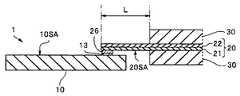
図1に示すように、配線板20は可撓性樹脂を基板23とし、銅等の導電体からなる複数の配線24を有するフレキシブル配線板である。配線24の先端部の接合電極(第2の電極)26が撮像素子10の半田バンプ13と接合されている。なお、以下の図において配線24は図示しない。 As shown in FIG. 1, the
そして、基板23は、熱膨張率αの異なる2種類の材料からなる基板21、22が積層されている積層基板である。例えば、第1の基板21は、厚さ20μmのポリイミド樹脂(α1=13ppm/K)であり、第2の基板22は、厚さ10μmのエポキシ樹脂(α2=65ppm/K)である。The
後述するように、熱膨張率αの異なる基板が積層されている基板23は、加熱されると、熱膨張率αが小さい基板21の側に湾曲変形する。すなわち、基板23は、樹脂からなるが、加熱されると湾曲変形する、いわゆるバイメタル機能を有する。このため、加熱により配線板20は湾曲変形する。 As will be described later, when the
配線24は基板23の片面に配設されているが、基板23の内部に配設されていてもよい。また配線板20は多層配線板でもよいし、チップコンデンサ等の電子部品が表面に実装されていてもよいし、電子部品が内蔵されていてもよい。 The
なお、図1に示したように、半導体モジュール1では、撮像素子10には、1つの配線板20が接合されている。すなわち、複数のバンプ13は受光面10SAの1端辺に沿って1列に配設されている。しかし、撮像素子10に複数の配線板20が接合されていてもよい。例えば複数のバンプ13が、対向する2端辺に沿って2列に配設されており、撮像素子に2つの配線板が接合されていてもよい。 As shown in FIG. 1, in the
撮像モジュール1は、半田接合温度への加熱により配線板20が湾曲変形することにより、配線24の先端部の接合電極(第2の電極)26が、撮像素子10のバンプ(第1の電極)13に圧接される。 In the
<半導体モジュールの製造方法>
次に、半導体モジュール1の製造方法について図2のフローチャートに沿って説明する。<Semiconductor module manufacturing method>
Next, the manufacturing method of the
<ステップS11>半導体素子作製工程
複数の受光部12と、それぞれの受光部12の周囲に列設された複数のバンプ135と、を受光面10SAに有する、シリコン等からなる半導体ウエハが作製される。<Step S11> Semiconductor Element Manufacturing Step A semiconductor wafer made of silicon or the like having a plurality of light receiving
低融点金属からなるバンプ13は、電気めっき法、ペースト印刷法、または、ボールはんだ搭載法等により配設される。 The
<ステップS12>配線板作製工程
所定の仕様のバイメタル機能を有する基板21と基板22とが積層された配線板20が作製される。配線板20は、半田接合温度への加熱により、接合電極26が配設された接合面20SAを内側に湾曲変形するように設計される。すなわち、接合面20SA側の第1の基板21の熱膨張係数α1よりも、接合面20SAと対向する面の第2の基板22の熱膨張係数α2が大きい。<Step S12> Wiring Board Manufacturing Step
加熱時の湾曲変形量は、(A)第1の基板21の熱膨張係数α1と第2の基板22の熱膨張係数α2との熱膨張係数比(=熱膨張係数α2/熱膨張係数α1)と、(B)第1の基板21の厚さと第2の基板22の厚さ、(C)湾曲変形可能な長さL(図3A等参照)で決まる。 The amount of bending deformation at the time of heating is (A) the thermal expansion coefficient ratio between the thermal expansion coefficient α1 of the
このため、(α1<α2)であれば良いが、熱膨張係数比が、1.5以上であることが好ましく、特に2以上が好ましい。熱膨張係数比の上限は、材料面の制約等から、例えば30である。 For this reason, (α1 <α2) may be satisfied, but the thermal expansion coefficient ratio is preferably 1.5 or more, particularly preferably 2 or more. The upper limit of the thermal expansion coefficient ratio is, for example, 30 due to material limitations and the like.
但し、第1の基板21の熱膨張係数α1は、配線24を構成する銅等の導電性金属と略同じ熱膨張係数のガラスエポキシ樹脂(α=15ppm/K)、またはポリイミド(α=13ppm/K)等であることが、配線24と第1の基板21との接着強度向上のために好ましい。 However, the thermal expansion coefficient α1 of the
第1の基板21と第2の基板22とは公知の各種材料から適宜選択される。例えば、第1の基板21としてガラスエポキシ樹脂(α=15ppm/K)を用い、第2の基板としてエポキシ樹脂(α=65ppm/K)を用いてもよい。また、第1の基板21および第2の基板22の少なくともいずれかが金属材料であってもよい。 The
さらに、基板23は、ともに金属からなる第1の基板21と第2の基板22とが積層されたバイメタルであり、配線24が配設される接合面20SAが絶縁性樹脂層(例えば、ポリイミド)により覆われていてもよい。すなわち、基板23は、3種以上の材料が積層された構造であり、その内の2層の熱膨張係数が異なっていればよい。 Further, the
バイメタルとしては、公知の低熱膨張金属、例えば、Fe−36Ni合金(α<1ppm/K)等からなる第1の基板21と、公知の金属、例えば、銅(α=16ppm/K)、鉄(α=12ppm/K)、銅合金、鉄合金、アルミニウム等からなる第2の基板22との組み合わせを用いる。 Examples of the bimetal include a
第1の基板21の厚さおよび第2の基板22の厚さは適宜選択される。また湾曲変形可能な長さLは、熱膨張係数比および第1の基板21の厚さおよび第2の基板22の厚さに応じて適宜選択される。例えば、第1の基板21の厚さおよび第2の基板22の厚さは10μm以上300μm以下であり、湾曲変形可能な長さLは、50μm以上10mm以下である。 The thickness of the
<ステップS13>近接配置工程
図3Aに示すように、配線板20を安定に保持するため、後端側が接合用治具30により挟持される。湾曲変形する長さLは適宜選択される。なお、接合用治具30は、配線板20の片面を吸着保持してもよい。<Step S13> Proximity Placement Step As shown in FIG. 3A, the rear end side is sandwiched by the joining
そして、配線板20の複数の接合電極26と、撮像素子10の複数のバンプ13との位置決めが行われ、接合電極26とバンプ13とが近接するように配置される。ここで、接合電極26とバンプ13との距離は100μm以下が好ましく、両者が接触していてもよい。 Then, the plurality of
なお、図3A等では説明を容易にするため、配線板20の先端部が大きく湾曲しているように図示しているが、実際には、ほぼ平坦であったり、少しうねりがあったりする程度である。 In order to facilitate the explanation in FIG. 3A and the like, the tip end portion of the
<ステップS13>接合工程
接合電極26とバンプ13とが近接するように配置された状態で、所定の半田接合温度への加熱が行われ、例えば、半田溶融温度よりも10℃高い温度に達するまで加熱される。<Step S13> Joining Step Heating to a predetermined solder joining temperature is performed in a state where the joining
すると、図3Bに示すように、加熱により、配線板20の第2の基板22が第1の基板21よりも大きく膨張するため、配線板20の先端側は接合面(20SA)側に湾曲変形する。変形量は、接合電極26が10μm以上100μm以下、バンプ13の方向に移動することが好ましい。それにより、接合電極26はバンプ13に圧接される。 Then, as shown in FIG. 3B, the
すなわち、半導体モジュール1の製造方法では、高価な接合装置を用いて外力を印加することなく、半田接合時に接合電極26はバンプ13に圧接する。このため、接合不良が発生しにくく、かつ、接合信頼性の高い半導体モジュール1を簡単な加熱接合装置で製造できる。 That is, in the method for manufacturing the
なお、半田接合温度への加熱により配線板20を湾曲変形するために、配線板20に形状記憶合金からなる基板を配設してもよい。また、上記実施形態では半導体素子として撮像素子10を例に説明したが、これに限られるものではない。 Note that a substrate made of a shape memory alloy may be disposed on the
また、上記実施形態においては、第1の電極13を半田バンプで形成し、第2の電極26を接合電極としたが、第2の電極26を半田バンプとして接合を行ってもよい。 Moreover, in the said embodiment, although the
<第2実施形態>
第2実施形態の半導体モジュール1Aおよび半導体モジュール1Aの製造方法は、半導体モジュール1等と類似しているので、同じ機能の構成要素には同じ符号を付し、説明は省略する。Second Embodiment
Since the
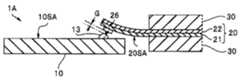
図4Aに示すように、半導体モジュール1Aの配線板20の接合電極26Aは、半田接合温度において溶融しない金属からなる高さGの突起部を有する、凸状電極である。 As shown in FIG. 4A, the bonding electrode 26A of the
このため、図4Bに示すように、接合時に溶融した半田の中に進入した接合電極26Aの突起部は、受光面10SAに当接する。半導体モジュール1Aでは、複数の接合部の状況が異なっていても、配線板20の接合面20SAと、撮像素子10の受光面10SAとの間隔は、全ての接合部において突起部の高さGとなる。突起部の高さGは、バンプ13の高さと同程度の40μm以上100μm以下が好ましい。 For this reason, as shown in FIG. 4B, the protruding portion of the bonding electrode 26A that has entered the solder melted during bonding contacts the light receiving surface 10SA. In the
接合電極26Aの突起部としては、例えば、スダッドバンプ、またはめっきバンプ等である。スダッドバンプは、ワイヤボンディング装置を用いて、金ワイヤの先端を放電溶融して形成した金ボールをボンディングパッドに金属接合した後にワイヤを切断することで作製される。めっきバンプとしては、半田バリア層であるニッケル層に覆われた銅バンプ等を用いる。 Examples of the protruding portion of the
半導体モジュール1Aは、半導体モジュール1の効果を有し、さらに、より接続信頼性が高い。 The
<第3実施形態>
第3実施形態の半導体モジュール1Bおよび半導体モジュール1Bの製造方法は、半導体モジュール1等と類似しているので、同じ機能の構成要素には同じ符号を付し、説明は省略する。<Third Embodiment>
Since the semiconductor module 1B and the manufacturing method of the semiconductor module 1B of the third embodiment are similar to the
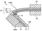
図5Aおよび図5Bに示すように、半導体モジュール1Bでは、複数の第1の電極である半田バンプ13が、撮像素子10Bのテーパー形状の側面10SSに配設されている。そして、撮像素子10Bの受光面10SAには、受光部12を保護するカバーガラスが透明接着剤により接着されている。バンプ13は、図示しない貫通配線等により受光部12と接続されている。 As shown in FIGS. 5A and 5B, in the semiconductor module 1B, the solder bumps 13 that are a plurality of first electrodes are arranged on the tapered side surface 10SS of the
半導体モジュール1Bは、複数の撮像素子10Bを含む半導体ウエハにガラスウエハを接合した接合ウエハを切断し個片化することで受光部12が保護された半導体素子が作製される。また、バンプ13が側面に配設されているため、撮像素子10Bの受光面10SAから接続された配線板20が側面から突出することがない。このため、半導体モジュール1Bは、半導体モジュール1よりも細径である。 In the semiconductor module 1B, a semiconductor element in which the
図5Bに示すようにバイメタル機能を有する配線板20は加熱により湾曲変形する。配線24の先端部の接合電極(第2の電極)26が、撮像素子10のバンプ(第1の電極)13に圧接されるため、半導体モジュール1Bは信頼性の高い接合が容易である。 As shown in FIG. 5B, the
<第4実施形態>
第4実施形態の半導体モジュール1Cおよび半導体モジュール1Cの製造方法は、半導体モジュール1等と類似しているので、同じ機能の構成要素には同じ符号を付し、説明は省略する。<Fourth embodiment>
Since the
図6Aに示すように半導体モジュール1Cでは、配線板20Cは、バイメタル機能を有していない通常の配線板である。しかし、接合用治具40の配線板20Cを保持する部分が、熱膨張係数がα1の第1の治具41と熱膨張係数がα2の第2の治具42とからなり、バイメタル機能を有する。すなわち、α1<α2である。 As shown in FIG. 6A, in the
例えば、第1の治具41として、厚さ100μmのFe−36Ni合金箔(α1<1ppm/K)を用い、第2の治具42として厚さ150μmのステンレス箔(α2=12ppm/K)を用いることができる。 For example, a 100 μm thick Fe-36Ni alloy foil (α1 <1 ppm / K) is used as the
図6Bに示すように、半田接合温度に加熱されると、バイメタル機能を有する接合用治具40が湾曲変形し、結果として挟持された配線板20Cも、湾曲変形する。 As shown in FIG. 6B, when heated to the solder bonding temperature, the
このため、半導体モジュール1Cおよび半導体モジュール1Cの製造方法は、半導体モジュール1および半導体モジュール1の製造方法の効果を有する。 For this reason, the manufacturing method of the
さらに、半導体モジュール1Cの配線板20Cは通常の配線板であるため、安価である。 Furthermore, since the
<変形例>
図7に示す、第4実施形態の変形例1の半導体モジュールでは、配線板20Dの接合電極(第2の電極)26Dが、半田接合温度において溶融しない金属からなる高さGの凸状電極である。<Modification>
In the semiconductor module of
そして、接合用治具40Dは、熱膨張係数の異なる2種類の金属箔41A、41Bが接合されたバイメタルからなる第1の治具43と、例えばSUSからなる第2の治具42とからなる。第1の治具43は加熱されると金属箔41Aの方向に湾曲変形する。 The joining
図示しないが、第1の治具43と第2の治具42とにより挟持された配線板20Dの接合電極26Dは、半田接合温度へと加熱されると、第2の治具42の湾曲変形により、半導体素子のバンプに圧接される。 Although not shown, when the
図8に示す、第4実施形態の変形例2の半導体モジュールでは、配線板20Eの接合電極(第2の電極)26Eが、半田接合温度において溶融しない2種類の金属からなる高さGの凸状電極である。すなわち、接合電極26Eは、銅パッド26E1の外周面の少なくともバンプ(第1の電極)13と接する面が、Ni/Au層26E2で覆われ、厚さがGである。 In the semiconductor module of Modification 2 of the fourth embodiment shown in FIG. 8, the bonding electrode (second electrode) 26 </ b> E of the
そして、接合用治具40Eは、熱膨張係数の異なる2種類の金属箔41A、41Bが接合されたバイメタルからなる先端部と、配線板20Eを吸着し保持する保持部45とからなる。 The joining
図示しないが、接合用治具40Eの保持部45により保持された配線板20Eの接合電極26Eは、半田接合温度に加熱されると、接合用治具40Eの先端部の湾曲変形により、半導体素子のバンプに圧接される。 Although not shown, when the
以上の説明のように、接合用治具40、40D、40Eは、撮像素子10に列設された複数のバンプ(第1の電極)13のそれぞれと、配線板20の複数の配線24のそれぞれの先端部の接合電極(第2の電極)26とを加熱しながら接合するために用いられる接合用治具であって、加熱されると保持した配線板20C、20D、20Eを湾曲変形させるバイメタル機能を有する。 As described above, the joining
本発明は上述した実施形態に限定されるものではなく、本発明の要旨を変えない範囲において、種々の変更、改変等ができる。 The present invention is not limited to the above-described embodiment, and various changes and modifications can be made without departing from the scope of the present invention.
1、1A〜1C…半導体モジュール
10…撮像素子
11…半導体チップ
12…受光部
13…半田バンプ(第1の電極)
20…フレキシブル配線板
24…配線
26…接合電極(第2の電極)
30、40…接合用治具DESCRIPTION OF
20 ...
30, 40 ... Joining jig
Claims (13)
Translated fromJapanese前記複数の第1の電極のそれぞれに、先端部の第2の電極が半田接合された複数の配線を有する可撓性の配線板と、を具備する半導体モジュールであって、
前記配線板が、熱膨張率の異なる複数の基板が積層されている積層基板を有し、
半田接合温度への加熱により前記配線板が前記複数の基板の熱膨張率差により湾曲変形することによって、前記第2の電極が前記第1の電極に圧接されることを特徴とする半導体モジュール。A semiconductor element in which a plurality of first electrodes are arranged;
To each of the plurality of firstelectrodes,a semiconductor module comprisesa flexible wiring board, a having a plurality of wiring where the second electrode tip portion is solderjoint,
The wiring board has a laminated substrate in which a plurality of substrates having different thermal expansion coefficients are laminated,
A semiconductor module, wherein the second electrode is pressed against the first electrode when the wiring board is bent and deformeddue to a difference in thermal expansion coefficient of the plurality of substrates by heating to a solder bonding temperature.
前記第2の電極が接合された前記第1の基板が前記第2の基板よりも、熱膨張率が小さいことを特徴とする請求項1に記載の半導体モジュール。The wiring board has the laminated substrate in which a first substrate and a second substrate having different thermal expansion coefficients are laminated,
The semiconductor module according to claim 1,wherein the first substrate to which the second electrode is bonded has a smaller coefficient of thermal expansion than the second substrate .
前記第2の電極が、前記半田接合温度において溶融しない金属からなる凸状電極であることを特徴とする請求項1から請求項3のいずれか1項に記載の半導体モジュール。 4. The semiconductor module according to claim 1, wherein the second electrode is a convex electrode made of a metal that does not melt at the solder bonding temperature. 5.
加熱されると、保持した前記配線板を湾曲変形させるバイメタル機能を有することを特徴とする接合用治具。 A bonding jig having a bimetal function of bending and deforming the held wiring board when heated.
それぞれが先端部に第2の電極を有する複数の配線と、前記複数の配線が列設された基板と、を有する可撓性の配線板を作製する工程と、 Producing a flexible wiring board each having a plurality of wirings each having a second electrode at the tip, and a substrate on which the plurality of wirings are arranged;
前記第1の電極と前記第2の電極とを近接配置する工程と、 Placing the first electrode and the second electrode close together;
前記半導体素子と前記配線板とを半田接合する工程と、を具備する半導体モジュールの製造方法であって、 Soldering the semiconductor element and the wiring board, and a method for manufacturing a semiconductor module comprising:
半田接合温度への加熱により、熱膨張率の異なる複数の基板が積層されている積層基板を有する前記配線板が前記複数の基板の熱膨張率差により湾曲変形することによって、前記第2の電極が前記第1の電極に圧接されることを特徴とする半導体モジュールの製造方法。 When the wiring board having a laminated substrate in which a plurality of substrates having different thermal expansion coefficients is laminated by heating to a solder bonding temperature, the second electrode is bent and deformed due to a difference in thermal expansion coefficient between the plurality of substrates. Is pressed against the first electrode. A method for manufacturing a semiconductor module, comprising:
前記半田接合する工程において、前記接合用治具が熱膨張率差により湾曲変形することを特徴とする請求項9に記載の半導体モジュールの製造方法。 10. The method of manufacturing a semiconductor module according to claim 9, wherein, in the solder bonding step, the bonding jig is bent and deformed due to a difference in thermal expansion coefficient.
前記第2の電極が、前記半田接合温度において溶融しない金属からなる凸状電極であることを特徴とする請求項8から請求項10のいずれか1項に記載の半導体モジュールの製造方法。 11. The method of manufacturing a semiconductor module according to claim 8, wherein the second electrode is a convex electrode made of a metal that does not melt at the solder bonding temperature. 11.
Priority Applications (3)
| Application Number | Priority Date | Filing Date | Title |
|---|---|---|---|
| JP2014084809AJP6348759B2 (en) | 2014-04-16 | 2014-04-16 | Semiconductor module, joining jig, and manufacturing method of semiconductor module |
| PCT/JP2015/052000WO2015159566A1 (en) | 2014-04-16 | 2015-01-26 | Semiconductor module, bonding jig, and semiconductor module manufacturing method |
| US15/284,714US9881890B2 (en) | 2014-04-16 | 2016-10-04 | Semiconductor module, bonding jig, and manufacturing method of semiconductor module |
Applications Claiming Priority (1)
| Application Number | Priority Date | Filing Date | Title |
|---|---|---|---|
| JP2014084809AJP6348759B2 (en) | 2014-04-16 | 2014-04-16 | Semiconductor module, joining jig, and manufacturing method of semiconductor module |
Publications (3)
| Publication Number | Publication Date |
|---|---|
| JP2015204446A JP2015204446A (en) | 2015-11-16 |
| JP2015204446A5 JP2015204446A5 (en) | 2017-05-25 |
| JP6348759B2true JP6348759B2 (en) | 2018-06-27 |
Family
ID=54323785
Family Applications (1)
| Application Number | Title | Priority Date | Filing Date |
|---|---|---|---|
| JP2014084809AActiveJP6348759B2 (en) | 2014-04-16 | 2014-04-16 | Semiconductor module, joining jig, and manufacturing method of semiconductor module |
Country Status (3)
| Country | Link |
|---|---|
| US (1) | US9881890B2 (en) |
| JP (1) | JP6348759B2 (en) |
| WO (1) | WO2015159566A1 (en) |
Families Citing this family (1)
| Publication number | Priority date | Publication date | Assignee | Title |
|---|---|---|---|---|
| WO2018193531A1 (en)* | 2017-04-19 | 2018-10-25 | オリンパス株式会社 | Endoscope, imaging module, and imaging module production method |
Family Cites Families (11)
| Publication number | Priority date | Publication date | Assignee | Title |
|---|---|---|---|---|
| US5760465A (en)* | 1996-02-01 | 1998-06-02 | International Business Machines Corporation | Electronic package with strain relief means |
| JPH10186393A (en)* | 1996-12-19 | 1998-07-14 | Shin Etsu Polymer Co Ltd | Connector for display inspection of liquid crystal display panel, and production therefor |
| US6040624A (en)* | 1997-10-02 | 2000-03-21 | Motorola, Inc. | Semiconductor device package and method |
| CN1125368C (en) | 1999-01-20 | 2003-10-22 | 时至准钟表股份有限公司 | Structure for mounting semiconductor device on liquid crystal display, and semiconductor device |
| JP4389471B2 (en)* | 2003-05-19 | 2009-12-24 | パナソニック株式会社 | Electronic circuit connection structure and connection method |
| US7423219B2 (en)* | 2004-06-11 | 2008-09-09 | Ibiden Co., Ltd. | Flex-rigid wiring board |
| JP2009147180A (en)* | 2007-12-17 | 2009-07-02 | Panasonic Corp | Optical device and manufacturing method thereof |
| JP2010205915A (en)* | 2009-03-03 | 2010-09-16 | Olympus Corp | Semiconductor device |
| JP2011049367A (en)* | 2009-08-27 | 2011-03-10 | Panasonic Corp | Substrate connecting structure and electronic device |
| KR20110124063A (en)* | 2010-05-10 | 2011-11-16 | 하나 마이크론(주) | Stacked Semiconductor Packages |
| JP5637249B2 (en) | 2013-04-24 | 2014-12-10 | 日本テキサス・インスツルメンツ株式会社 | Ultrasonic bonding method |
- 2014
- 2014-04-16JPJP2014084809Apatent/JP6348759B2/enactiveActive
- 2015
- 2015-01-26WOPCT/JP2015/052000patent/WO2015159566A1/enactiveApplication Filing
- 2016
- 2016-10-04USUS15/284,714patent/US9881890B2/enactiveActive
Also Published As
| Publication number | Publication date |
|---|---|
| JP2015204446A (en) | 2015-11-16 |
| WO2015159566A1 (en) | 2015-10-22 |
| US9881890B2 (en) | 2018-01-30 |
| US20170025372A1 (en) | 2017-01-26 |
Similar Documents
| Publication | Publication Date | Title |
|---|---|---|
| JP5660263B1 (en) | Electronic component, method for manufacturing electronic component, and circuit board | |
| JP5452273B2 (en) | Semiconductor device | |
| JP6000859B2 (en) | Semiconductor device manufacturing method, semiconductor device, and endoscope | |
| JP6021618B2 (en) | Imaging apparatus, endoscope, and manufacturing method of imaging apparatus | |
| WO2004047173A1 (en) | Semiconductor package and laminated semiconductor package | |
| JP6416200B2 (en) | Imaging apparatus and manufacturing method of imaging apparatus | |
| JP6401237B2 (en) | Imaging apparatus and manufacturing method of imaging apparatus | |
| JP4751714B2 (en) | Stacked mounting structure | |
| CN107889344A (en) | Flexible printed circuit device | |
| JP2013219468A (en) | Image pickup module | |
| JP6348759B2 (en) | Semiconductor module, joining jig, and manufacturing method of semiconductor module | |
| JPWO2016166809A1 (en) | Imaging module and imaging module manufacturing method | |
| WO2010070779A1 (en) | Anisotropic conductive resin, substrate connecting structure and electronic device | |
| JP5388601B2 (en) | Electronic component storage package | |
| JP6504762B2 (en) | Module manufacturing method | |
| JP2007227452A (en) | Flexible wiring board, solder bonding method thereof, and optical transmission package using the same | |
| JP6641079B2 (en) | Printed circuit board manufacturing method and conductive member joining method | |
| JP2005244116A (en) | Manufacturing method of semiconductor device | |
| WO2017066896A1 (en) | Electrical connection structure between the front and rear of a chip, and manufacturing method therefor | |
| WO2016157376A1 (en) | Image pickup device and endoscope | |
| JP7033285B2 (en) | Fine wiring joint and its manufacturing method | |
| CN111742623A (en) | Metal-sheet-attached wiring board and method for manufacturing metal-sheet-attached wiring board | |
| JP5423246B2 (en) | Substrate module and manufacturing method thereof | |
| JP2005072098A (en) | Semiconductor device | |
| JP2009059800A (en) | Small module |
Legal Events
| Date | Code | Title | Description |
|---|---|---|---|
| A521 | Request for written amendment filed | Free format text:JAPANESE INTERMEDIATE CODE: A523 Effective date:20170331 | |
| A621 | Written request for application examination | Free format text:JAPANESE INTERMEDIATE CODE: A621 Effective date:20170331 | |
| TRDD | Decision of grant or rejection written | ||
| A01 | Written decision to grant a patent or to grant a registration (utility model) | Free format text:JAPANESE INTERMEDIATE CODE: A01 Effective date:20180515 | |
| A61 | First payment of annual fees (during grant procedure) | Free format text:JAPANESE INTERMEDIATE CODE: A61 Effective date:20180601 | |
| R151 | Written notification of patent or utility model registration | Ref document number:6348759 Country of ref document:JP Free format text:JAPANESE INTERMEDIATE CODE: R151 | |
| R250 | Receipt of annual fees | Free format text:JAPANESE INTERMEDIATE CODE: R250 | |
| R250 | Receipt of annual fees | Free format text:JAPANESE INTERMEDIATE CODE: R250 | |
| R250 | Receipt of annual fees | Free format text:JAPANESE INTERMEDIATE CODE: R250 | |
| R250 | Receipt of annual fees | Free format text:JAPANESE INTERMEDIATE CODE: R250 | |
| R250 | Receipt of annual fees | Free format text:JAPANESE INTERMEDIATE CODE: R250 |