JP6348468B2 - Wireless power receiver and terminal - Google Patents
Wireless power receiver and terminalDownload PDFInfo
- Publication number
- JP6348468B2 JP6348468B2JP2015172306AJP2015172306AJP6348468B2JP 6348468 B2JP6348468 B2JP 6348468B2JP 2015172306 AJP2015172306 AJP 2015172306AJP 2015172306 AJP2015172306 AJP 2015172306AJP 6348468 B2JP6348468 B2JP 6348468B2
- Authority
- JP
- Japan
- Prior art keywords
- wireless power
- coil
- connection terminal
- magnetic substrate
- power receiving
- Prior art date
- Legal status (The legal status is an assumption and is not a legal conclusion. Google has not performed a legal analysis and makes no representation as to the accuracy of the status listed.)
- Active
Links
Images


Classifications
- H—ELECTRICITY
- H02—GENERATION; CONVERSION OR DISTRIBUTION OF ELECTRIC POWER
- H02J—CIRCUIT ARRANGEMENTS OR SYSTEMS FOR SUPPLYING OR DISTRIBUTING ELECTRIC POWER; SYSTEMS FOR STORING ELECTRIC ENERGY
- H02J50/00—Circuit arrangements or systems for wireless supply or distribution of electric power
- H02J50/005—Mechanical details of housing or structure aiming to accommodate the power transfer means, e.g. mechanical integration of coils, antennas or transducers into emitting or receiving devices
- H02J5/005—
- B—PERFORMING OPERATIONS; TRANSPORTING
- B60—VEHICLES IN GENERAL
- B60L—PROPULSION OF ELECTRICALLY-PROPELLED VEHICLES; SUPPLYING ELECTRIC POWER FOR AUXILIARY EQUIPMENT OF ELECTRICALLY-PROPELLED VEHICLES; ELECTRODYNAMIC BRAKE SYSTEMS FOR VEHICLES IN GENERAL; MAGNETIC SUSPENSION OR LEVITATION FOR VEHICLES; MONITORING OPERATING VARIABLES OF ELECTRICALLY-PROPELLED VEHICLES; ELECTRIC SAFETY DEVICES FOR ELECTRICALLY-PROPELLED VEHICLES
- B60L53/00—Methods of charging batteries, specially adapted for electric vehicles; Charging stations or on-board charging equipment therefor; Exchange of energy storage elements in electric vehicles
- B60L53/10—Methods of charging batteries, specially adapted for electric vehicles; Charging stations or on-board charging equipment therefor; Exchange of energy storage elements in electric vehicles characterised by the energy transfer between the charging station and the vehicle
- B60L53/12—Inductive energy transfer
- G—PHYSICS
- G06—COMPUTING OR CALCULATING; COUNTING
- G06K—GRAPHICAL DATA READING; PRESENTATION OF DATA; RECORD CARRIERS; HANDLING RECORD CARRIERS
- G06K19/00—Record carriers for use with machines and with at least a part designed to carry digital markings
- G06K19/06—Record carriers for use with machines and with at least a part designed to carry digital markings characterised by the kind of the digital marking, e.g. shape, nature, code
- G06K19/067—Record carriers with conductive marks, printed circuits or semiconductor circuit elements, e.g. credit or identity cards also with resonating or responding marks without active components
- G06K19/07—Record carriers with conductive marks, printed circuits or semiconductor circuit elements, e.g. credit or identity cards also with resonating or responding marks without active components with integrated circuit chips
- G06K19/0723—Record carriers with conductive marks, printed circuits or semiconductor circuit elements, e.g. credit or identity cards also with resonating or responding marks without active components with integrated circuit chips the record carrier comprising an arrangement for non-contact communication, e.g. wireless communication circuits on transponder cards, non-contact smart cards or RFIDs
- H—ELECTRICITY
- H01—ELECTRIC ELEMENTS
- H01F—MAGNETS; INDUCTANCES; TRANSFORMERS; SELECTION OF MATERIALS FOR THEIR MAGNETIC PROPERTIES
- H01F27/00—Details of transformers or inductances, in general
- H01F27/28—Coils; Windings; Conductive connections
- H01F27/2804—Printed windings
- H—ELECTRICITY
- H01—ELECTRIC ELEMENTS
- H01F—MAGNETS; INDUCTANCES; TRANSFORMERS; SELECTION OF MATERIALS FOR THEIR MAGNETIC PROPERTIES
- H01F27/00—Details of transformers or inductances, in general
- H01F27/28—Coils; Windings; Conductive connections
- H01F27/29—Terminals; Tapping arrangements for signal inductances
- H—ELECTRICITY
- H01—ELECTRIC ELEMENTS
- H01F—MAGNETS; INDUCTANCES; TRANSFORMERS; SELECTION OF MATERIALS FOR THEIR MAGNETIC PROPERTIES
- H01F27/00—Details of transformers or inductances, in general
- H01F27/34—Special means for preventing or reducing unwanted electric or magnetic effects, e.g. no-load losses, reactive currents, harmonics, oscillations, leakage fields
- H01F27/36—Electric or magnetic shields or screens
- H01F27/366—Electric or magnetic shields or screens made of ferromagnetic material
- H—ELECTRICITY
- H01—ELECTRIC ELEMENTS
- H01F—MAGNETS; INDUCTANCES; TRANSFORMERS; SELECTION OF MATERIALS FOR THEIR MAGNETIC PROPERTIES
- H01F38/00—Adaptations of transformers or inductances for specific applications or functions
- H01F38/14—Inductive couplings
- H—ELECTRICITY
- H01—ELECTRIC ELEMENTS
- H01F—MAGNETS; INDUCTANCES; TRANSFORMERS; SELECTION OF MATERIALS FOR THEIR MAGNETIC PROPERTIES
- H01F41/00—Apparatus or processes specially adapted for manufacturing or assembling magnets, inductances or transformers; Apparatus or processes specially adapted for manufacturing materials characterised by their magnetic properties
- H01F41/14—Apparatus or processes specially adapted for manufacturing or assembling magnets, inductances or transformers; Apparatus or processes specially adapted for manufacturing materials characterised by their magnetic properties for applying magnetic films to substrates
- H—ELECTRICITY
- H02—GENERATION; CONVERSION OR DISTRIBUTION OF ELECTRIC POWER
- H02J—CIRCUIT ARRANGEMENTS OR SYSTEMS FOR SUPPLYING OR DISTRIBUTING ELECTRIC POWER; SYSTEMS FOR STORING ELECTRIC ENERGY
- H02J50/00—Circuit arrangements or systems for wireless supply or distribution of electric power
- H02J50/10—Circuit arrangements or systems for wireless supply or distribution of electric power using inductive coupling
- H02J50/12—Circuit arrangements or systems for wireless supply or distribution of electric power using inductive coupling of the resonant type
- H—ELECTRICITY
- H02—GENERATION; CONVERSION OR DISTRIBUTION OF ELECTRIC POWER
- H02J—CIRCUIT ARRANGEMENTS OR SYSTEMS FOR SUPPLYING OR DISTRIBUTING ELECTRIC POWER; SYSTEMS FOR STORING ELECTRIC ENERGY
- H02J50/00—Circuit arrangements or systems for wireless supply or distribution of electric power
- H02J50/70—Circuit arrangements or systems for wireless supply or distribution of electric power involving the reduction of electric, magnetic or electromagnetic leakage fields
- H02J7/025—
- H—ELECTRICITY
- H04—ELECTRIC COMMUNICATION TECHNIQUE
- H04B—TRANSMISSION
- H04B5/00—Near-field transmission systems, e.g. inductive or capacitive transmission systems
- H04B5/20—Near-field transmission systems, e.g. inductive or capacitive transmission systems characterised by the transmission technique; characterised by the transmission medium
- H04B5/24—Inductive coupling
- H04B5/26—Inductive coupling using coils
- H—ELECTRICITY
- H04—ELECTRIC COMMUNICATION TECHNIQUE
- H04B—TRANSMISSION
- H04B5/00—Near-field transmission systems, e.g. inductive or capacitive transmission systems
- H04B5/70—Near-field transmission systems, e.g. inductive or capacitive transmission systems specially adapted for specific purposes
- H04B5/79—Near-field transmission systems, e.g. inductive or capacitive transmission systems specially adapted for specific purposes for data transfer in combination with power transfer
- H—ELECTRICITY
- H04—ELECTRIC COMMUNICATION TECHNIQUE
- H04W—WIRELESS COMMUNICATION NETWORKS
- H04W4/00—Services specially adapted for wireless communication networks; Facilities therefor
- H04W4/80—Services using short range communication, e.g. near-field communication [NFC], radio-frequency identification [RFID] or low energy communication
- Y—GENERAL TAGGING OF NEW TECHNOLOGICAL DEVELOPMENTS; GENERAL TAGGING OF CROSS-SECTIONAL TECHNOLOGIES SPANNING OVER SEVERAL SECTIONS OF THE IPC; TECHNICAL SUBJECTS COVERED BY FORMER USPC CROSS-REFERENCE ART COLLECTIONS [XRACs] AND DIGESTS
- Y02—TECHNOLOGIES OR APPLICATIONS FOR MITIGATION OR ADAPTATION AGAINST CLIMATE CHANGE
- Y02T—CLIMATE CHANGE MITIGATION TECHNOLOGIES RELATED TO TRANSPORTATION
- Y02T10/00—Road transport of goods or passengers
- Y02T10/60—Other road transportation technologies with climate change mitigation effect
- Y02T10/70—Energy storage systems for electromobility, e.g. batteries
- Y—GENERAL TAGGING OF NEW TECHNOLOGICAL DEVELOPMENTS; GENERAL TAGGING OF CROSS-SECTIONAL TECHNOLOGIES SPANNING OVER SEVERAL SECTIONS OF THE IPC; TECHNICAL SUBJECTS COVERED BY FORMER USPC CROSS-REFERENCE ART COLLECTIONS [XRACs] AND DIGESTS
- Y02—TECHNOLOGIES OR APPLICATIONS FOR MITIGATION OR ADAPTATION AGAINST CLIMATE CHANGE
- Y02T—CLIMATE CHANGE MITIGATION TECHNOLOGIES RELATED TO TRANSPORTATION
- Y02T10/00—Road transport of goods or passengers
- Y02T10/60—Other road transportation technologies with climate change mitigation effect
- Y02T10/7072—Electromobility specific charging systems or methods for batteries, ultracapacitors, supercapacitors or double-layer capacitors
- Y—GENERAL TAGGING OF NEW TECHNOLOGICAL DEVELOPMENTS; GENERAL TAGGING OF CROSS-SECTIONAL TECHNOLOGIES SPANNING OVER SEVERAL SECTIONS OF THE IPC; TECHNICAL SUBJECTS COVERED BY FORMER USPC CROSS-REFERENCE ART COLLECTIONS [XRACs] AND DIGESTS
- Y02—TECHNOLOGIES OR APPLICATIONS FOR MITIGATION OR ADAPTATION AGAINST CLIMATE CHANGE
- Y02T—CLIMATE CHANGE MITIGATION TECHNOLOGIES RELATED TO TRANSPORTATION
- Y02T90/00—Enabling technologies or technologies with a potential or indirect contribution to GHG emissions mitigation
- Y02T90/10—Technologies relating to charging of electric vehicles
- Y02T90/12—Electric charging stations
- Y—GENERAL TAGGING OF NEW TECHNOLOGICAL DEVELOPMENTS; GENERAL TAGGING OF CROSS-SECTIONAL TECHNOLOGIES SPANNING OVER SEVERAL SECTIONS OF THE IPC; TECHNICAL SUBJECTS COVERED BY FORMER USPC CROSS-REFERENCE ART COLLECTIONS [XRACs] AND DIGESTS
- Y02—TECHNOLOGIES OR APPLICATIONS FOR MITIGATION OR ADAPTATION AGAINST CLIMATE CHANGE
- Y02T—CLIMATE CHANGE MITIGATION TECHNOLOGIES RELATED TO TRANSPORTATION
- Y02T90/00—Enabling technologies or technologies with a potential or indirect contribution to GHG emissions mitigation
- Y02T90/10—Technologies relating to charging of electric vehicles
- Y02T90/14—Plug-in electric vehicles
- Y—GENERAL TAGGING OF NEW TECHNOLOGICAL DEVELOPMENTS; GENERAL TAGGING OF CROSS-SECTIONAL TECHNOLOGIES SPANNING OVER SEVERAL SECTIONS OF THE IPC; TECHNICAL SUBJECTS COVERED BY FORMER USPC CROSS-REFERENCE ART COLLECTIONS [XRACs] AND DIGESTS
- Y02—TECHNOLOGIES OR APPLICATIONS FOR MITIGATION OR ADAPTATION AGAINST CLIMATE CHANGE
- Y02T—CLIMATE CHANGE MITIGATION TECHNOLOGIES RELATED TO TRANSPORTATION
- Y02T90/00—Enabling technologies or technologies with a potential or indirect contribution to GHG emissions mitigation
- Y02T90/10—Technologies relating to charging of electric vehicles
- Y02T90/16—Information or communication technologies improving the operation of electric vehicles
- Y—GENERAL TAGGING OF NEW TECHNOLOGICAL DEVELOPMENTS; GENERAL TAGGING OF CROSS-SECTIONAL TECHNOLOGIES SPANNING OVER SEVERAL SECTIONS OF THE IPC; TECHNICAL SUBJECTS COVERED BY FORMER USPC CROSS-REFERENCE ART COLLECTIONS [XRACs] AND DIGESTS
- Y10—TECHNICAL SUBJECTS COVERED BY FORMER USPC
- Y10T—TECHNICAL SUBJECTS COVERED BY FORMER US CLASSIFICATION
- Y10T29/00—Metal working
- Y10T29/49—Method of mechanical manufacture
- Y10T29/49002—Electrical device making
- Y10T29/4902—Electromagnet, transformer or inductor
Landscapes
- Engineering & Computer Science (AREA)
- Power Engineering (AREA)
- Computer Networks & Wireless Communication (AREA)
- Signal Processing (AREA)
- Physics & Mathematics (AREA)
- General Physics & Mathematics (AREA)
- Theoretical Computer Science (AREA)
- Computer Hardware Design (AREA)
- Microelectronics & Electronic Packaging (AREA)
- Manufacturing & Machinery (AREA)
- Electromagnetism (AREA)
- Mechanical Engineering (AREA)
- Transportation (AREA)
- Coils Or Transformers For Communication (AREA)
- Near-Field Transmission Systems (AREA)
- Parts Printed On Printed Circuit Boards (AREA)
- Manufacturing Cores, Coils, And Magnets (AREA)
- Charge And Discharge Circuits For Batteries Or The Like (AREA)
Description
Translated fromJapanese本発明は、無線電力受信機および端末に関し、より詳しくは、無線電力転送またはアンテナに適用されて全体厚さを減少させ、製造工程を単純化させた無線電力受信機および端末に関する。The present invention relates to awireless power receiver and the terminal, and more particularly, to reduce the overall thickness is applied to the wireless power transfer or antenna, to awireless power receiver and the terminal obtained by simplifying the manufacturing process.
無線で電気エネルギーを所望の機器に伝達する無線電力転送技術(wireless power transmissionまたはwireless energy transfer)は、既に1800年代に電磁気誘導原理を用いた電気モーターや変圧器が使われ始めており、その後にはラジオ波やレーザーのような電磁波を放射して電気エネルギーを転送する方法も試みられてきた。私達がよく使用する電動歯ブラシや一部無線カミソリも実際は電磁気誘導原理により充電される。電磁気誘導は導体の周辺で磁場を変化させた時、電圧が誘導されて電流が流れる現象をいう。電磁気誘導方式は小型機器を中心に常用化が速く進行されているが、電力の転送距離が短いという問題がある。 Wireless power transfer technology (wireless power transmission or wireless energy transfer) that wirelessly transfers electrical energy to the desired device has already begun to use electric motors and transformers that use the principle of electromagnetic induction in the 1800s. Attempts have also been made to transfer electrical energy by emitting electromagnetic waves such as radio waves and lasers. Electric toothbrushes and some wireless razors that we often use are actually charged by the electromagnetic induction principle. Electromagnetic induction is a phenomenon in which when a magnetic field is changed around a conductor, voltage is induced and current flows. The electromagnetic induction method is being used frequently mainly in small devices, but has a problem that the power transfer distance is short.
現在まで無線方式によるエネルギー伝達方式は電磁気誘導の以外に共振及び短波長無線周波数を用いた遠距離送信技術などがある。 To date, wireless energy transmission methods include long-distance transmission technology using resonance and short-wavelength radio frequencies in addition to electromagnetic induction.
しかしながら、一般的に端末機に内蔵された無線電力受信装置は厚さが厚く、製造工程が複雑であるという問題がある。 However, the wireless power receiving apparatus built in the terminal is generally thick and has a problem that the manufacturing process is complicated.
本発明は、磁性基板の上面にコイル部を直接配置させて無線電力受信装置の厚さを格段に減少させることができる方法の提供を目的とする。 An object of the present invention is to provide a method capable of significantly reducing the thickness of a wireless power receiver by arranging a coil portion directly on an upper surface of a magnetic substrate.
本発明は、磁性基板の上面にコイル部及び近距離通信アンテナを直接配置させて高い電力転送効率を維持させ、外部装置との通信も可能にする方法の提供を目的とする。 It is an object of the present invention to provide a method for arranging a coil unit and a short-range communication antenna directly on the upper surface of a magnetic substrate to maintain high power transfer efficiency and to enable communication with an external device.
本発明は、磁性基板の上面にコイル部を直接配置させて無線電力受信装置の製造工程を単純化させた方法の提供を目的とする。 An object of the present invention is to provide a method that simplifies the manufacturing process of a wireless power receiver by arranging a coil portion directly on an upper surface of a magnetic substrate.
本発明は、磁性基板の内部にコイル部を配置させて無線電力受信装置の厚さを格段に減少させることができる方法の提供を目的とする。 It is an object of the present invention to provide a method capable of significantly reducing the thickness of a wireless power receiving apparatus by arranging a coil portion inside a magnetic substrate.
本発明は、磁性基板の内部にコイル部を配置させ、近距離通信アンテナを磁性基板に配置させて高い電力転送効率を維持させ、外部装置との通信も可能にする方法の提供を目的とする。 It is an object of the present invention to provide a method for arranging a coil portion inside a magnetic substrate and arranging a short-range communication antenna on the magnetic substrate to maintain high power transfer efficiency and to enable communication with an external device. .
本発明は、磁性基板の内部にコイル部を配置させて無線電力受信装置の製造工程を単純化させた方法の提供を目的とする。 An object of the present invention is to provide a method that simplifies the manufacturing process of a wireless power receiver by arranging a coil portion inside a magnetic substrate.
本発明の一実施形態に係る無線電力受信装置は、磁性基板及び前記磁性基板の上に導電パターンまたは導電層として形成され、無線で電力を受信するためのコイルを含むことを特徴とする。 A wireless power receiver according to an embodiment of the present invention includes a magnetic substrate and a coil that is formed as a conductive pattern or a conductive layer on the magnetic substrate and receives power wirelessly.
本発明の更に他の実施形態に係る無線電力受信装置は磁性基板及び前記磁性基板に導電パターンまたは導電層として形成され、無線で電力を受信するためのコイルを含み、前記コイルの一部が前記磁性基板の内部に配置されたことを特徴とする。 A wireless power receiver according to still another embodiment of the present invention includes a magnetic substrate and a coil that is formed on the magnetic substrate as a conductive pattern or a conductive layer and receives power wirelessly, and a part of the coil is the It is arranged inside the magnetic substrate.
本発明の一実施形態に係る無線で電力を受信する無線電力受信装置の製造方法は、導電体と保護フィルムを付着させるステップと、前記導電体をエッチングして導電パターンを形成するステップと、前記導電パターンの連結端子に外部回路と連結するための連結部を接続させるステップと、磁性基板に前記連結部に対応する収容空間を形成するステップと、前記磁性基板を前記連結部が前記収容空間に位置するようにして前記導電パターンの上に配置するステップとを含む。 According to an embodiment of the present invention, there is provided a method of manufacturing a wireless power receiving apparatus that wirelessly receives power, attaching a conductor and a protective film, etching the conductor to form a conductive pattern, Connecting a connecting portion for connecting to an external circuit to the connecting terminal of the conductive pattern; forming a receiving space corresponding to the connecting portion on the magnetic substrate; and connecting the magnetic substrate to the receiving space. And disposing the conductive pattern on the conductive pattern.
本発明の一実施形態によれば、磁性基板の上面にコイル部を直接配置させて無線電力受信装置の厚さを格段に減少させることができる。 According to an embodiment of the present invention, the thickness of the wireless power receiver can be significantly reduced by arranging the coil portion directly on the top surface of the magnetic substrate.
本発明の一実施形態によれば、磁性基板の上面にコイル部及び近距離通信アンテナを直接配置させて高い電力転送効率を維持させ、同時に外部装置との通信も可能にする。 According to an embodiment of the present invention, the coil unit and the short-range communication antenna are directly disposed on the upper surface of the magnetic substrate to maintain high power transfer efficiency, and at the same time, communication with an external device is enabled.
本発明の一実施形態によれば、ラミネーティング及びエッチング過程のみを通じて磁性基板の上面にコイル部を直接配置させて無線電力受信装置の製造工程を単純化させることができる。 According to an embodiment of the present invention, the manufacturing process of the wireless power receiver can be simplified by arranging the coil part directly on the top surface of the magnetic substrate only through the laminating and etching processes.
本発明の一実施形態によれば、磁性基板の内部に導電パターンを形成して無線電力受信装置の厚さを格段に減少させることができる。 According to an embodiment of the present invention, a conductive pattern can be formed inside a magnetic substrate to significantly reduce the thickness of the wireless power receiver.
本発明の一実施形態によれば、磁性基板の内部に導電パターンを形成して高い電力転送効率を有することができ、同時に近距離通信アンテナを用いて外部装置との通信も可能にする。 According to an embodiment of the present invention, a conductive pattern can be formed inside a magnetic substrate to have high power transfer efficiency, and at the same time, communication with an external device can be performed using a short-range communication antenna.
本発明の一実施形態によれば、連結部が磁性基板の収容空間に配置されることによって連結部の厚さだけ無線電力受信装置の全体厚さが格段に減少できる。 According to the embodiment of the present invention, the entire thickness of the wireless power receiving apparatus can be significantly reduced by the thickness of the connecting portion by arranging the connecting portion in the accommodation space of the magnetic substrate.
本発明の一実施形態によれば、連結部にテープ部材を使用して、無線電力受信装置の全体サイズを縮めることができる。 According to one embodiment of the present invention, it is possible to reduce the overall size of the wireless power receiving apparatus by using a tape member for the connecting portion.
本発明の一実施形態によれば、連結部にリードフレームを使用して、発熱、外部の湿気、衝撃などから連結部に含まれた配線層が保護され、量産が可能な効果を得ることができる。 According to an embodiment of the present invention, a lead frame is used for the connecting portion, and the wiring layer included in the connecting portion is protected from heat generation, external moisture, impact, and the like, and an effect of enabling mass production can be obtained. it can.
本発明の一実施形態によれば、磁性基板の内部に形成された導電パターンによって、外部に向ける磁場の方向をコイル部側に変更させて電力転送効率を上げることができ、同時に外部に漏出される磁場の量を減少させて、人体の有害性を有する磁場の影響を最小化することができる。 According to an embodiment of the present invention, the conductive pattern formed inside the magnetic substrate can change the direction of the magnetic field directed to the outside to the coil part side to increase the power transfer efficiency, and is leaked to the outside at the same time. The amount of magnetic field generated can be reduced to minimize the influence of the magnetic field that is harmful to the human body.
本発明の一実施形態によれば、パターン溝を形成する過程及びコイル部を挿入する過程のみを通じて無線電力受信装置を製造することができるので製造工程が単純化される効果がある。 According to an embodiment of the present invention, since the wireless power receiving apparatus can be manufactured only through the process of forming the pattern groove and the process of inserting the coil unit, the manufacturing process is simplified.
一方、その他の多様な効果は後述する本発明の実施形態に係る詳細な説明で直接的または暗示的に開示される。 Meanwhile, various other effects are disclosed directly or implicitly in the detailed description of the embodiments of the present invention described later.
以下、添付した図面を参照して本発明の好ましい実施形態に対して本発明が属する技術分野で通常の知識を有する者が容易に実施できるように詳細に説明する。
以下、導電パターンは、導電層の形態を意味することができるし、パターニング工程によって形成された構造を意味することもできる。導電層は、導電パターンと代替可能な意味で使用することができるし、パターニング、エッチング、配置、選別的なメッキ工程を含んで形成された構造を意味することもできる。Hereinafter, preferred embodiments of the present invention will be described in detail with reference to the accompanying drawings so that those skilled in the art can easily carry out the invention.
Hereinafter, the conductive pattern may mean the form of the conductive layer, or may mean the structure formed by the patterning process. The conductive layer can be used as an alternative to the conductive pattern, and can also mean a structure formed by including patterning, etching, arrangement, and selective plating processes.
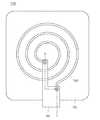
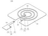
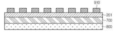
図1は本発明の第1実施形態に係る無線電力受信装置1000の斜視図であり、図2は本発明の第1実施形態に係る無線電力受信装置1000の平面図であり、図3は図2の連結部300に図示した点線に沿ってAからA'に切った場合、無線電力受信装置1000の断面図である。 FIG. 1 is a perspective view of a wireless
図1乃至図3を参考すると、無線電力受信装置1000は、磁性基板100、コイル部200、及び連結部300を含むことができる。 1 to 3, the wireless
無線電力受信装置1000は、送信側から無線で電力を受信することができる。一実施形態において、無線電力受信装置1000は電磁気誘導を用いて無線で電力を受信することができる。一実施形態において、無線電力受信装置1000は共振を用いて無線で電力を受信することができる。 The wireless
電磁気誘導及び共振とも磁場を用いて電力を転送する方式である。 Both electromagnetic induction and resonance are systems in which electric power is transferred using a magnetic field.
磁性基板100は送信側から伝達される磁場の方向を変更させることができる。 The
磁性基板100は送信側から伝達される磁場の方向を変更させて外部に漏出できる磁場の量を減少させることができる。これによって、遮蔽効果を有することができる。 The
磁性基板100は、送信側から伝達される磁場の方向を側方に変更させてコイル部200に磁場がさらに集中的に伝達できるようにする。 The
磁性基板100は、送信側から伝達される磁場のうち、外部に漏出される磁場を吸収して熱にて放出させることができる。外部に漏出される磁場の量が減少すれば、人体に有害な影響を及ぼす状況が防止できる。 The
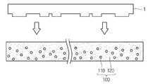
図3を参考すると、磁性基板100は磁性体110及び支持体120を含むことができる。 Referring to FIG. 3, the
磁性体110は、粒子またはセラミックの形態を含むことができる。 The
支持体120は、熱硬化性樹脂または熱可塑性樹脂を含むことができる。 The
磁性基板100はシート(Sheet)形態に構成され、フレキシブル(flexible)な性質を有することができる。 The
また、図1を説明すると、コイル部200は、第1連結端子210、第2連結端子220、及びコイル230を含むことができる。コイル230は、導電層または導電パターンを形成することができる。 Referring to FIG. 1, the
第1連結端子210はコイル230の一端に、第2連結端子220はコイル230の他端に位置する。 The
第1連結端子210及び第2連結端子220は、連結部300との接続のために必要な端子である。 The
コイル230は、1つの導線が複数回巻線されたコイルパターンを形成することができる。一実施形態において、コイルパターンは平面螺旋構造であるが、これに限定されるものではなく、多様なパターンを形成することができる。 The
コイル部200は、磁性基板100の上面に直接配置される。一実施形態において、コイル部200と磁性基板100との間には接着層(図示せず)がさらに配置できる。 The
コイル部200は、導電体を含むことができる。導電体は、金属または合金が用いられる。一実施形態において、金属は銀または銅が使われ、これに限定されるものではない。 The
コイル部200は送信側から無線で受信した電力を連結部300に伝達することができる。コイル部200は、送信側から電磁気誘導または共振を用いて電力を受信することができる。 The
連結部300は、第1連結端子310、第2連結端子320、及び印刷回路基板330を含むことができる。 The
連結部300の第1連結端子310はコイル部200の第1連結端子210と接続され、連結部300の第2連結端子320はコイル部200の第2連結端子220と接続される。 The
印刷回路基板330は配線層を含むことができ、配線層は後出の受信回路などが配置できる。 The printed
連結部300は、受信回路(図示せず)とコイル部200との間を連結してコイル部200から伝達された電力を受信回路(図示せず)を通じて負荷(図示せず)に伝達することができる。受信回路は、交流電力を直流電力に変換する整流回路及び変換された直流電力からリップル成分を除去して負荷に伝達する平滑回路を含むことができる。 The connecting
図2乃至図3は、コイル部200と連結部300とが連結された状態の場合、本発明の第1実施形態に係る無線電力受信装置1000の詳細な構成を説明するための図である。 2 to 3 are diagrams for explaining a detailed configuration of the wireless
図2は、本発明の第1実施形態に係る無線電力受信装置1000の平面図である。 FIG. 2 is a plan view of the wireless
図2は、コイル部200と連結部300とが互いに接続されている状態を示す。 FIG. 2 shows a state where the
一実施形態において、コイル部200と連結部300との間の接続はソルダーによりなされる。具体的に、コイル部200の第1連結端子210と連結部300の第1連結端子310は第1ソルダー10により連結され、コイル部200の第2連結端子220と連結部300の第2連結端子320は第2ソルダー20により連結される。具体的に、コイル部200の第1連結端子210は第1ソルダー10のビアホールを通じて連結部300の第1連結端子310と連結され、コイル部200の第2連結端子220は第2ソルダー20のビアホールを通じて連結部300の第2連結端子320と連結される。 In one embodiment, the connection between the
図2に図示された無線電力受信装置1000は端末機などの電子機器に内蔵できる。 The wireless
端末機は、セルラーフォン、PCS(Personal Communication Servie)フォン、GSMフォン(登録商標)、CDMA−2000フォン、WCDMAフォン(登録商標)などの通常的な移動電話機、PMP(Portable Multimedia Player)、PDA(Personal Digital Assistants)、スマートフォン、MBS(Mobile Broadcast System)フォンであるが、これに限定されるものではなく、無線で電力を受信することができる如何なる装置でも構わない。 The terminal is a normal mobile phone such as a cellular phone, a PCS (Personal Communication Servie) phone, a GSM phone (registered trademark), a CDMA-2000 phone, a WCDMA phone (registered trademark), a PMP (Portable Multimedia Player), a PDA (PDA). Personal Digital Assistants), smart phones, and MBS (Mobile Broadcast System) phones, but are not limited to this, and any device that can receive power wirelessly may be used.
図2の連結部300に図示された点線に沿ってAからA'に切った断面に対しては図3で説明する。 The cross section cut from A to A ′ along the dotted line shown in the connecting
図3は、図2の連結部300に図示された点線に沿ってAからA’に切った場合、無線電力受信装置1000の断面図である。 FIG. 3 is a cross-sectional view of the wireless
図3を参考すると、磁性基板100の上面にはコイル部200の構成要素である第1連結端子210、第2連結端子220、及びコイル230が配置されている。 Referring to FIG. 3, a
本発明の第1実施形態に係る無線電力受信装置1000は、磁性基板100の上面にコイル部200が直接配置されているので、既存のFPCBの上にコイルパターンを形成した場合とは異なり、全体的な厚さを格段に減少させることができる。 In the wireless
好ましくは、磁性基板100の厚さは0.43mmであり、コイル部200の厚さは0.1mmであり、これを合せた厚さは0.53mmでありうる。しかしながら、この数値は例示に過ぎない。 Preferably, the thickness of the
即ち、コイル部200を導電体、導電パターン、薄膜のような形態に構成することによって、無線電力受信装置1000の厚さを減少させることができる。これは、この頃、携帯用端末機のようにスリム化を要求している電子機器に適用すれば、携帯用端末機の全体厚さを減少させながら送信側から電力を受信するのに有用な効果をもたらすことができる。 That is, the thickness of the wireless
コイル部200の上側には連結部300が直接配置されている。コイル部200の上側に連結部300が直接配置されることによって、コイル部200と連結部300とが容易に接続できる。 The connecting
コイル部200の第1連結端子210は、ソルダー10により連結部300の第1連結端子310と接続される。 The
コイル部200の第2連結端子220は、ソルダー20により連結部300の第2連結端子320と接続される。 The
コイル230の幅(W)と厚さ(T)は所定の値を有するように設計される。コイル230とコイル230との間の間隔も所定の距離値を有するように設計される。 The width (W) and thickness (T) of the
図4乃至図8は、本発明の一実施形態に係る無線電力受信装置1000の製造方法を説明するための図である。 4 to 8 are diagrams for explaining a method of manufacturing the wireless
無線電力受信装置1000の構成は、図1乃至図3で説明したものと本質的に結合できる。 The configuration of the wireless
まず、図4を参考すると、磁性基板100が形成される。 First, referring to FIG. 4, the
次に、図5を参考すると、磁性基板100の上面に直接導電体201を積層させる。一実施形態では、磁性基板100の上面に接着層が積層された後、導電体201が積層されることもできる。 Next, referring to FIG. 5, the
一実施形態において、磁性基板100の上面に導電体201を積層させる方法は、導電体201を所定の温度で加熱し、その後、所定の圧力を加えるラミネーティング(laminating)工程が使用できる。ラミネーティング(laminating)工程とは、熱と圧力を用いて互いに異なる種類の金属箔、紙などを接着させる工程を意味する。 In one embodiment, the method of laminating the
次に、図6を参考すると、導電体201の上面にマスク500が積層される。マスク500は、コイル部200の第1連結端子210、第2連結端子220、及びコイル230が形成される位置の上面のみに積層できる。 Next, referring to FIG. 6, a
次に、図7を参考すると、図6の状態でエッチング液に漬ければマスク500が位置しない溝部分がエッチングされる。すると、導電体201は一定の導電パターンを形成するようになる。 Next, referring to FIG. 7, if the substrate is immersed in an etching solution in the state of FIG. 6, the groove portion where the
その後、マスク500を除去すれば、無線電力受信装置1000のコイル部200が形成される。 Then, if the
次に、図8を参考すると、コイル部200と連結部300とが接続されるようにソルダリング作業を経る。 Next, referring to FIG. 8, a soldering operation is performed so that the
即ち、コイル部200の第1連結端子210と連結部300の第3連結端子310とをソルダー10により接続させ、コイル部200の第2連結端子200と連結部300の第2連結端子320とをソルダー20により接続させる。 That is, the
前記のように磁性基板100の上面に直接コイル部200を配置させることによって、無線電力受信装置1000の全体厚さを格段に減少させることができ、ラミネーティングとエッチング過程のみを通じて無線電力受信装置1000が製造できるので、工程が単純化される効果がある。 By arranging the
図9は、図2の連結部300に図示された点線に沿ってAからA’に切った場合、本発明の第2実施形態に係る無線電力受信装置1000の断面図である。 FIG. 9 is a cross-sectional view of the wireless
図9を参考すると、無線電力受信装置1000は、磁性基板100、コイル部200、連結部300、及び接着層700を含むことができる。 Referring to FIG. 9, the wireless
磁性基板100、コイル部200、及び連結部300は、図1で説明したものと同一である。 The
接着層700は、磁性基板100とコイル部200との間に配置されて磁性基板100とコイル部200とを接着させる。 The
図10は、本発明の第3実施形態に係る無線電力受信装置1000の平面図である。 FIG. 10 is a plan view of a
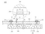
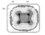
図10を参考すると、無線電力受信装置1000は、磁性基板100、コイル部200、連結部300、及び近距離通信アンテナ600を含むことができる。 Referring to FIG. 10, the wireless
磁性基板100、コイル部200、及び連結部300に対する説明は、図1乃至図3で説明したものと同一である。 The description of the
近距離通信アンテナ600は、第1連結端子610、第2連結端子620、及び外郭コイル630を含む。 The short-
近距離通信アンテナ600の第1連結端子610及び第2連結端子620は連結部300に接続される。 The
近距離通信アンテナ600は、近距離無線通信が可能なリーダ器と通信を遂行することができる。近距離通信アンテナ600は、前記リーダ器と情報を送受信するアンテナの役割を遂行する。 The near
一実施形態において、近距離通信アンテナ600はコイル部200の外郭に配置される。一実施形態において、コイル部200が磁性基板100の中央に配置された場合、近距離通信アンテナ600はコイル部200を覆いかぶせるように磁性基板100の外郭に沿って配置される。近距離通信アンテナ600は1つの導線が複数回巻線された四角形の構造を有することができるが、これに限定されるものではない。 In one embodiment, the short-
近距離通信アンテナ600は、コイル部200のように、導電パターン、導電層を形成することができる。 The short-
近距離通信アンテナ600で使われる近距離通信規格は多様な技術が使用できるが、NFC(Near Field Commnication)を用いることが好ましい。NFC(Near Field Commnication)は、13.56MHzの帯域を有し、近い距離の無線通信を行うための技術である。 Although various technologies can be used for the near field communication standard used in the near
近距離通信アンテナ600は、磁性基板100の上面に直接配置される。 The short-
近距離通信アンテナ600が磁性基板100に配置される方法は、前記図4で説明した製造方法と同一である。 The method of disposing the short-
次に、図11乃至図13で本発明の第4実施形態に係る無線電力受信装置1000の詳細な構成を説明する。 Next, a detailed configuration of the wireless
図11は、本発明の第4実施形態に係る無線電力受信装置1000の斜視図である。 FIG. 11 is a perspective view of a
図11を参考すると、無線電力受信装置1000は、磁性基板100、コイル部200、及び連結部300を含む。 Referring to FIG. 11, the wireless
コイル部200及び連結部300に対する説明は、図1で説明したものと同一である。但し、磁性基板100の場合、一部の構造が異なるので、これを中心として説明する。 The description of the
図11を参考すると、磁性基板100は連結部300の構造と同一構造を有する収容領域130を形成している。即ち、図1の場合、磁性基板100の上面にコイル部200が配置され、コイル部200の上に連結部300が連結される構造であるが、図11の場合、磁性基板100の自体に連結部300の構造と同一構造に該当する部分だけ収容領域130が形成されて、コイル部200の下側に連結部300が配置される。 Referring to FIG. 11, the
図12は、本発明の第4実施形態に係る無線電力受信装置1000の平面図である。 FIG. 12 is a plan view of a
図12は、コイル部200と連結部300とが互いに接続されている状態を示す。 FIG. 12 shows a state where the
連結部300の厚さは磁性基板100の厚さと等しいか小さいことがある。連結部300はフレキシブルな印刷回路基板(FPCB:Flexible PCB)で具現できる。 The thickness of the connecting
連結部300は、磁性基板100の収容領域130に配置される。 The connecting
連結部300の厚さが磁性基板100の厚さと等しいか小さければ、図3の実施形態とは異なり、連結部300の厚さだけ無線電力受信装置1000の全体厚さが減少する。また、磁性基板100が収容領域130だけ磁性体110及び支持体120が少なく必要であるので、費用上の利点がある。 If the thickness of the connecting
図13は、図12の連結部300に図示された点に沿ってBからB'に切った場合、無線電力受信装置1000の断面図である。 FIG. 13 is a cross-sectional view of the wireless
連結部300の厚さは磁性基板100の厚さより小さい場合を仮定して説明する。 The description will be made assuming that the thickness of the connecting
図13を参考すると、連結部300の上面にはコイル部200の構成要素である第1連結端子210、第2連結端子220、及びコイル230が配置されている。 Referring to FIG. 13, a
コイル部200の下側には連結部300が配置されている。 A connecting
コイル部200の第1連結端子210は、ソルダー10により連結部300の第1連結端子310と接続される。 The
コイル部200の第2連結端子220は、ソルダー20により連結部300の第2連結端子320と接続される。 The
コイル230の幅(W)と厚さ(T)は所定の値を有するように設計される。コイル230とコイル230との間の間隔も所定の距離値を有するように設計される。 The width (W) and thickness (T) of the
図13を参考すると、連結部300の厚さが磁性基板100の厚さより小さいので、図3の実施形態とは異なり、連結部300の厚さだけ無線電力受信装置1000の全体厚さが減少する。また、磁性基板100が図10で図示した収容領域130だけ磁性体110及び支持体120が少なく必要であるので、費用上の利点がある。 Referring to FIG. 13, since the thickness of the connecting
次に、図14乃至図20で本発明の第5実施形態に係る無線電力受信装置1000について詳細に説明する。 Next, a wireless
図14は本発明の第5実施形態に係る無線電力受信装置1000の斜視図であり、図15は本発明の第5実施形態に係る無線電力受信装置1000の平面図であり、図16は本発明の第5実施形態に係る無線電力受信装置1000をCからC'に切った断面図であり、図17乃至図21は本発明の第5実施形態に係る無線電力受信装置1000の製造方法を説明するための図である。 FIG. 14 is a perspective view of a wireless
まず、図14を参照すると、本発明の第5実施形態に係る無線電力受信装置1000は、磁性基板100、コイル部200、及び連結部300を含むことができる。 First, referring to FIG. 14, the
一実施形態において、無線電力受信装置1000は送信側から電磁気誘導により電力を受信することができる。この場合、コイル部200のコイル230は送信側のコイルと電磁気誘導により無線で電力を受信することができる。 In one embodiment, the wireless
一実施形態において、無線電力受信装置1000は送信側から共振により電力を受信することができる。この場合、コイル部200のコイル230は送信側の送信共振コイルと共振周波数で動作して電力を受信する受信共振コイル及び受信共振コイルとカップリングされて伝達を受けた電力を受信回路に伝達する受信誘導コイルを含むことができる。 In one embodiment, the wireless
磁性基板100は、送信側から伝達される磁場の方向を変更させることができる。 The
磁性基板100は、送信側から伝達される磁場の方向を変更させて外部に漏出できる磁場の量を減少させることができる。これによって、遮蔽効果を有することができる。 The
磁性基板100は、送信側から伝達される磁場の方向を側方に変更させてコイル部200に磁場がさらに集中的に伝達できるようにする。 The
磁性基板100は送信側から伝達される磁場のうち、外部に漏出される磁場を吸収して熱にて放出させることもできる。外部に漏出される磁場の量が減少すれば、人体に有害な影響を及ぼす状況が防止できる。 The
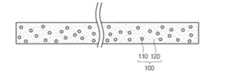
図16を参考すると、磁性基板100は磁性体110及び支持体120を含むことができる。 Referring to FIG. 16, the
磁性体110は、粒子またはセラミックの形態を含むことができる。一実施形態において、磁性体110は、スピネルタイプ、ヘキサタイプ、センダストタイプ、パーマロイタイプの磁性体のうちのいずれか1つでありうる。 The
支持体120は熱硬化性樹脂または熱可塑性樹脂を含むことができ、磁性基板100を支持する役割を遂行する。 The
磁性基板100はシート(Sheet)形態に構成されることができ、フレキシブル(flexible)な性質を有することができる。 The
また、図14を説明すると、コイル部200は、第1連結端子210、第2連結端子220、及びコイル230を含むことができる。コイル230は、導電層または導電パターンを形成することができる。 Referring to FIG. 14, the
コイル部200は、磁性基板100の内部に配置される。具体的に、コイル部200は、磁性基板100の内部に陥没されて配置される。より具体的に、磁性基板100はパターン溝を含むことができ、前記パターン溝には前記コイル部200が配置される。前記パターン溝は、前記コイル部200が形成する導電パターンまたは導電層の形態と同一な形態を有することができる。 The
コイル部200の厚さは磁性基板100の厚さより小さく、コイル部200の上側は磁性基板100の外部に露出できる。 The thickness of the
磁性基板100にコイル部200及び連結部300が配置されて無線電力受信装置1000が製造される工程は、図17乃至図21で後述する。 A process of manufacturing the wireless
コイル部200の第1連結端子210はコイル230の一端に、第2連結端子220はコイル230の他端に位置する。 The
コイル部200の第1連結端子210及び第2連結端子220は、連結部300との接続のために必要な端子である。 The
コイル230は、1つの導線が複数回巻線されたパターンを形成することができる。一実施形態において、パターンは平面螺旋構造であるが、これに限定されるものではなく、多様なパターンを形成することができる。 The
コイル部200は送信側から無線で受信した電力を連結部300に伝達することができる。コイル部200は、送信側から電磁気誘導または共振を用いて受信した電力を連結部300に伝達することができる。 The
連結部300は、第1連結端子310、第2連結端子320、及び印刷回路基板330を含むことができる。 The
連結部300の第1連結端子310はコイル部200の第1連結端子210と接続され、連結部300の第2連結端子320はコイル部200の第2連結端子220と接続される。 The
印刷回路基板330は配線層を含むことができ、配線層は後出の受信回路などを含むことができる。 The printed
連結部300は、受信回路(図示せず)とコイル部200との間を連結してコイル部200から伝達された電力を受信回路を通じて負荷(図示せず)に伝達することができる。受信回路は、交流電力を直流電力に変換する整流回路(図示せず)及び変換された直流電力からリップル成分を除去して負荷に伝達する平滑回路(図示せず)を含むことができる。 The connecting
図15乃至図16は、コイル部200と連結部300とが連結された状態の場合、本発明の第5実施形態に係る無線電力受信装置1000の詳細な構成を説明するための図である。 15 to 16 are diagrams for explaining a detailed configuration of the wireless
図15は、コイル部200と連結部300とが互いに接続されている状態を示す。 FIG. 15 shows a state where the
コイル部200と連結部300との間の接続はソルダーによりなされる。 Connection between the
図16を参照すると、コイル部200の第1連結端子210と連結部300の第1連結端子310とは第1ソルダー10により連結され、コイル部200の第2連結端子220と連結部300の第2連結端子320とは第2ソルダー20により連結される。具体的に、コイル部200の第1連結端子210は第1ソルダー10のビアホールを通じて連結部300の第1連結端子310と連結され、コイル部200の第2連結端子220は第2ソルダー20のビアホールを通じて連結部300の第2連結端子320と連結される。 Referring to FIG. 16, the
一実施形態において、前記ビアホールはレーザーを用いて形成される。この際、レーザー、はUVレーザー、CO2レーザーなどが用いられる。 In one embodiment, the via hole is formed using a laser. In this case, a UV laser, a CO2 laser, or the like is used as the laser.
図16を参照すると、磁性基板100及びコイル部200が連結部300と接続されている無線電力受信装置1000の断面図が図示されている。 Referring to FIG. 16, a cross-sectional view of the
即ち、磁性基板100のパターン溝140にはコイル部200の構成要素である第1連結端子210、第2連結端子220、及びコイル230が配置される。 That is, the first connecting
また、磁性基板100及びコイル部200が連結部300と接続されている状態が図示されている。 Further, a state in which the
コイル230の幅(W)と厚さ(T)、及び磁性基板100の厚さ(T1)は所定の値を有するように設計される。一実施形態において、コイル230の厚さは0.1mm、磁性基板100の厚さは0.43mmであるが、これは例示に過ぎない。一実施形態において、コイル230の厚さ(T)は磁性基板100の厚さ(T1)より小さいことがある。 The width (W) and thickness (T) of the
本発明の第5実施形態に係る無線電力受信装置1000は、磁性基板100のパターン溝140にコイル部200が直接配置されているので、コイル部200の厚さだけ無線電力受信装置1000が取り付けられた電子機器の全体厚さが減少できる。本発明の第5実施形態を携帯用端末機のような無線電力受信装置1000を取り付けている電子機器に適用すれば、スリム化が要求されている携帯用端末機の全体厚さを減少させる効果が得られる。 In the wireless
また、本発明の第5実施形態に係る無線電力受信装置1000は、磁性基板100のパターン溝140にコイル部200が配置されているので、既存のFPCBの上にコイルパターンを形成した場合とは異なり、無線電力受信装置1000が取り付けられた電子機器の全体サイズが減少できる。 Further, in the wireless
図17乃至図21は、本発明の第5実施形態に係る無線電力受信装置1000の製造方法を説明するための図である。 17 to 21 are diagrams for explaining a method of manufacturing the wireless
以下、図14乃至図16の内容と結び付けて、本発明の第5実施形態に係る無線電力受信装置1000の製造方法を説明する。 Hereinafter, a method for manufacturing the wireless
まず、図17を参照すると、磁性基板100が配置される。一実施形態において、磁性基板100はポリエチレン系ゴムの上にセンダスト(sendust)合金系(Al、Fe、SiO2)金属粉末を塗布し、表面に酸化被膜を形成して製造できる。 First, referring to FIG. 17, the
次に、図18を参照すると、磁性基板100にコイル部200を収容することができるパターン溝を形成するために金型1を用いて熱と圧力を同時に加える。金型1は、コイル部200の形状と同じように製作される。一実施形態において、金型1の材料には、アルミニウム合金、銅合金、鋳鉄などが使用できる。 Next, referring to FIG. 18, heat and pressure are simultaneously applied using the
金型1には無線で電力を受信するためのコイル部200が配置される位置に対応した突出部が形成される。 The
金型1を用いて熱を加える時、磁性基板100の構成要素であるセンダスト合金系金属粉末の特性を考慮して特定温度を有する熱を加える。一実施形態において、磁性基板100が前記ポリエチレン系ゴムの上にセンダスト(sendust)合金系金属粉末を塗布して製造された場合、金型1を用いて熱と圧力を加える時、100度以上180度以下の温度で高圧に圧力を加えた後、100度以下の温度に冷却させた後、磁性基板100から金型1を分離する。金型1を用いて磁性基板100に圧力を加えた後、金型1を直ちに分離するようになれば、パターン溝140に残っている熱によって所望のパターン溝140が形成されないことがあるので、100度以下に冷却させた後、磁性基板100から金型1を分離させる必要がある。 When heat is applied using the
仮に、磁性基板100にセンダスト合金系金属粉末を使用する場合、粉末の配列、密度などによって加える温度と圧力が変わることがある。即ち、粉末の配列が均一でない場合には、より高い温度と圧力を加えなければならず、粉末の配列が均一な場合には粉末の配列が均一でない場合に比べてより低い温度及び圧力を加えてもよい。また、粉末の密度の低い場合には、高い場合に比べてより低い温度及び圧力を加えてもよい。また、粉末の成分、即ち粉末を構成する合金によって加えられる温度及び圧力が変わることもある。 If a sendust alloy metal powder is used for the
このように、粉末の配列、密度、成分によって加えられる温度は差が出ることがある。 Thus, the applied temperature may vary depending on the powder arrangement, density, and ingredients.
一実施形態において、金型1を用いて熱と圧力を加える代わり、磁性基板100にコイル部200を収容することができるパターン溝を形成するためにレーザーを照射することができる。パターン溝は、紫外線領域の波長を有するレーザービームを発射するエキシマーレーザー(excimer laser)を使用して形成される。前記エキシマーレーザーはKrFエキシマーレーザー(クリプトン弗素、中心波長248?)またはArFエキシマーレーザー(アルゴン弗素、中心波長193nm)などが使用できる。 In one embodiment, instead of applying heat and pressure using the
次に、図19を参照すると、図19は金型1を磁性基板100から分離時、パターン溝140が形成された磁性基板100の状態を示す。 Next, referring to FIG. 19, FIG. 19 shows a state of the
次に、図20を参照すると、図19の状態で磁性基板100に形成されたパターン溝140にコイル部200を挿入する。コイル部200が挿入されれば、磁性基板100のパターン溝140は一定の導電パターンが形成される。 Next, referring to FIG. 20, the
一実施形態において、磁性基板100のパターン溝140にコイル部200が挿入される過程はメッキまたはコイル部200が形成する導電パターンを有するようにエッチング過程を経た金属を挿入する方法が使用できる。 In an exemplary embodiment, the process of inserting the
具体的に、メッキはパターン溝140を金属物質で充填する工程を通じてコイル部200が形成される。この際、前記金属物質は、Cu、Ag、Sn、Au、Ni、及びPdのうちから選択されるいずれか1つの物質であり、前記金属物質の充填は無電解メッキ、電解メッキ、スクリーン印刷(Screen Printing)、スパッタリング(Sputtering)、蒸発法(Ecaporation)、インクジェッティング、及びディスフェンシングのうちのいずれか1つまたはこれらの組み合わせられた方式を利用することができる。 Specifically, the
次に、図21を参照すると、コイル部200と連結部300とが接続されるようにソルダリング作業を経る。 Next, referring to FIG. 21, a soldering operation is performed so that the
即ち、コイル部200の第1連結端子210と連結部300の第1連結端子310とをソルダー10により接続させ、コイル部200の第2連結端子220と連結部300の第2連結端子320とをソルダー20により接続させる。 That is, the
このように、本発明の第5実施形態に係る無線電力受信装置1000の製造方法は、磁性基板100にパターン溝を形成し、形成されたパターン溝にコイル部200を配置させることによって、無線電力受信装置1000の全体厚さを減少させることができ、パターン溝を形成する過程及びコイル部を挿入する過程のみを通じて無線電力受信装置1000を製造することができるので、製造工程が単純化される効果がある。 As described above, in the method for manufacturing the
図22は本発明の第1実施形態によって磁性基板の上面にコイル部を配置した場合、使用周波数によるコイル部のインダクタンス、抵抗、及びQ値の変化を説明するための図であり、図23は本発明の第5実施形態によって磁性基板の内部のパターン溝にコイル部を配置した場合、使用周波数によるコイル部200のインダクタンス、抵抗、及びQ値の変化を説明するための図である。 FIG. 22 is a diagram for explaining changes in inductance, resistance, and Q value of the coil portion depending on the use frequency when the coil portion is disposed on the top surface of the magnetic substrate according to the first embodiment of the present invention. It is a figure for demonstrating the change of the inductance of the
コイル部200のインダクタンス、抵抗、及びQ値の関係式は、次の<数式1>により表現できる。 The relational expression of the inductance, resistance, and Q value of the
(数1)
Q=w*L/R(Equation 1)
Q = w * L / R
<数式1>で、wは電力転送時に使われる周波数であり、Lはコイル部200のインダクタンス、Rはコイル部200の抵抗を表す。 In
<数式1>から確認できるように、コイル部200のインダクタンスはその値が増加するほどQ値が高まる。Q値が増加すれば、電力転送効率が良くなる。コイル部200の抵抗はコイル部200の自体で発生する電力損失量を数値化したものであり、その値が小さいほどQ値が増加する。 As can be confirmed from
図22及び図23を参照すると、使用周波数が150kHzの時を比較すると、本発明の第1実施形態によって磁性基板100の上面にコイル部200を配置した場合に比べて、図23は本発明の第5実施形態によって磁性基板100の内部のパターン溝140にコイル部200を配置した場合、コイル部200のインダクタンスは約9986.92umから約10339.34umに、352.42umだけ増加し、コイル部200の抵抗は約0.910オームから約0.853オームに、0.057オームだけ減少したことを確認することができる。結局、インダクタンスの増加及び抵抗の減少量だけQ値が増加する。 Referring to FIG. 22 and FIG. 23, comparing the case where the operating frequency is 150 kHz, FIG. 23 shows the present invention compared to the case where the
したがって、本発明の第5実施形態に係る無線電力受信装置1000は、磁性基板100の内部のパターン溝にコイル部200を配置して、Q値を高めることができる。 Therefore, the
図24は本発明の第1実施形態によって磁性基板の上面にコイル部を配置した場合、磁場の放射パターンを示すためのH−Fieldであり、図25は本発明の第5実施形態によって磁性基板の内部のパターン溝にコイル部を配置した場合、磁場の放射パターンを示すためのH−Fieldである。 FIG. 24 shows an H-Field for showing a radiation pattern of a magnetic field when a coil part is arranged on the upper surface of the magnetic substrate according to the first embodiment of the present invention. FIG. 25 shows a magnetic substrate according to the fifth embodiment of the present invention. This is an H-Field for showing a radiation pattern of a magnetic field when a coil portion is arranged in a pattern groove inside the.
図24及び図25を参照すると、磁性基板100の内部のパターン溝にコイル部200を配置した場合が磁性基板100の上面にコイル部を配置した場合に比べて、コイル部200の外側でより多い磁場が放射されることを確認することができる。これは、磁性基板100の内部にコイル部200が陥没された構造により外部に向ける磁場の方向をコイル部200の側方に変更させるためである。 Referring to FIGS. 24 and 25, the case where the
また、磁性基板100の内部のパターン溝にコイル部200を配置した場合が磁性基板100の上面にコイル部200を配置した場合に比べて、コイル部200の内側でより多い磁場が放射されることを確認することができる。このまた、磁性基板100の内部にコイル部200が陥没された構造により外部に向ける磁場の方向をコイル部200の側方に変更させるためである。 Further, when the
図24及び図25を参照すると、無線電力受信装置1000は近距離通信アンテナ600をさらに含むことができる。 Referring to FIGS. 24 and 25, the wireless
近距離通信アンテナ600は近距離無線通信が可能なリーダ器と通信を遂行することができる。近距離通信アンテナ600は、前記リーダ器と情報を送受信するアンテナの役割を遂行する。 The near
一実施形態において、近距離通信アンテナ600はコイル部200の外郭に配置される。一実施形態において、コイル部200が磁性基板100の中央に配置された場合、近距離通信アンテナ600はコイル部200を覆いかぶせるように磁性基板100の外郭に沿って配置される。近距離通信アンテナ600は、1つの導線が複数回巻線された四角形の構造を有することができるが、これに限定されるものではない。 In one embodiment, the short-
近距離通信アンテナ600は、コイル部200のように、導電パターン、導電層を形成することができる。 The short-
近距離通信アンテナ600で使われる近距離通信の規格は多様な技術が使用できるが、NFC(Near Field Commnication)を用いることが好ましい。 Although various technologies can be used for the short-range communication standard used in the short-
次に、図26乃至図37を参照して本発明の更に他の実施形態に係る無線電力受信装置について説明する。 Next, a wireless power receiving apparatus according to still another embodiment of the present invention will be described with reference to FIGS.
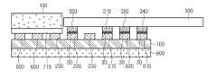
図26は本発明の更に他の実施形態に係る無線電力受信装置1000の分解斜視図であり、図27は本発明の更に他の実施形態に係る無線電力受信装置1000の斜視図であり、図28は本発明の更に他の実施形態に係る無線電力受信装置1000の断面図である。 FIG. 26 is an exploded perspective view of a
一方、図27は図26に図示された無線電力受信装置1000の構成要素を結合して置いた斜視図であり、一部の構成要素が省略されて結合した形態を有する。 On the other hand, FIG. 27 is a perspective view in which the constituent elements of the wireless
本発明の更に他の実施形態に係る無線電力受信装置1000は、携帯用端末機などの電子機器に装着できる。 The wireless
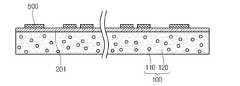
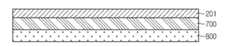
図26乃至図28を参照すると、無線電力受信装置1000は、磁性基板100、コイル部200、連結部300、近距離通信アンテナ600、接着層700、第1両面接着層710、第2両面接着層720、保護フィルム800、及び剥離紙層730を含むことができる。 26 to 28, the wireless
まず、図26を参照すると、磁性基板100は送信側から伝達される磁場の方向を変更させることができる。 First, referring to FIG. 26, the
磁性基板100は送信側からコイル部200が伝達を受ける磁場の方向を変更させて外部に漏出できる磁場の量を減少させることができる。これによって、遮蔽効果を有することができる。 The
磁性基板100は送信側から伝達される磁場の方向を側方に変更させてコイル部200に磁場がより集中的に伝達できるようにする。 The
磁性基板100は送信側からコイル部200が伝達を受ける磁場のうち、外部に漏出される磁場を吸収して熱にて放出させることもできる。外部に漏出される磁場の量が減少されれば、人体に有害な影響を及ぼす状況が防止できる。 The
図28を参考すると、磁性基板100は磁性体110及び支持体120を含むことができる。 Referring to FIG. 28, the
磁性体110は粒子またはセラミックの形態を含むことができる。一実施形態において、磁性体110は、スピネルタイプ、ヘキサタイプ、センダストタイプ、パーマロイタイプの磁性体のうちのいずれか1つでありうる。 The
支持体120は熱硬化性樹脂または熱可塑性樹脂を含むことができ、磁性基板100を支持する役割を遂行する。 The
また、図26を説明すれば、磁性基板100はシート(Sheet)形態に構成されることができ、フレキシブル(flexible)な性質を有することができる。 Referring to FIG. 26, the
磁性基板100は一定領域に収容空間130を有することができる。収容空間130は連結部300の形態と同一形態を有することができ、連結部300は前記収容空間130に配置されてコイル部200と接続できる。 The
コイル部200は送信側から電磁気誘導または共振を用いて無線で電力を受信することができる。コイル部200は、図1で説明したように、第1連結端子210、第2連結端子220、及びコイル230を含むことができる。コイル230は、導電層または導電パターンで形成される。 The
連結部300は、コイル部200と受信回路(図示せず)との間を連結してコイル部200から伝達された電力を受信回路を通じて負荷(図示せず)に伝達することができる。 The connecting
連結部300は配線層を含むことができ、配線層は前記受信回路を含むことができる。前記受信回路はコイル部200から伝達された電力を整流する整流回路、ノイズ信号を除去する平滑回路、及び無線で電力を受信するための全般的な動作を遂行するメインICチップを含むことができる。 The
また、前記受信回路は、近距離通信アンテナ600から受信した信号を近距離通信信号処理部(図示せず)に伝達することができる。 In addition, the receiving circuit can transmit a signal received from the near
連結部300は、磁性基板100の収容空間130に配置されてコイル部200と接続可能である。図27を共に参照すると、磁性基板100の収容空間130に連結部300が配置されたことを確認することができる。 The connecting
連結部300は、第1連結端子310、第2連結端子320、第3連結端子340、及び第4連結端子350を含むことができ、連結部300の第1連結端子310はコイル部200の第1連結端子210と接続され、連結部300の第2連結端子320はコイル部200の第2連結端子220と接続され、連結部300の第3連結端子340は近距離通信アンテナ600の第1連結端子610と接続され、連結部300の第4連結端子350は近距離通信アンテナ600の第2連結端子620と接続される。 The
連結部300は収容空間130の形態と同一な形態を有して収容空間130に配置される。連結部300が磁性基板100の収容空間130に配置されることによって、連結部300の厚さだけ無線電力受信装置1000の全体厚さが格段に減少できる。これによって、無線電力受信装置1000が取り付けられた携帯用端末機などの電子機器の厚さも格段に減少できる。 The connecting
一実施形態において、連結部300はフレキシブルな印刷回路基板(FPCB:Flexible Printed Circuit)またはテープ部材(TS:Tape Substrate)またはリードフレーム(LF:Lead Frame)が使用できる。連結部300にテープ部材を使用する場合、連結部300の厚さが減少して無線電力受信装置1000の全体サイズを縮めることができる。 In an exemplary embodiment, the
連結部300にリードフレームを使用する場合、発熱、外部の湿気、衝撃などから、連結部300に含まれた配線層が保護され、量産が可能であるという長所がある。 When a lead frame is used for the connecting
また、図26を説明すると、近距離通信アンテナ600は近距離無線通信が可能なリーダ器と通信を遂行することができる。近距離通信アンテナ600は、前記リーダ器と情報を送受信する役割を遂行することができる。 26, the short-
近距離通信信号処理部(図示せず)は、連結部300を通じて近距離通信アンテナ600で受信した信号の伝達を受けて処理することができる。 A near field communication signal processing unit (not shown) can receive and process a signal received by the near
近距離通信アンテナ600で使われる近距離通信規格は多様な技術が使用できるが、NFC(Near Field Commnication)を用いることが好ましい。 Although various technologies can be used for the near field communication standard used in the near
一実施形態において、近距離通信アンテナ600はコイル部200の外郭に配置される。図27を参照すると、コイル部200が磁性基板100の上に配置された場合、近距離通信アンテナ600はコイル部200を覆いかぶせるように磁性基板100の外郭に沿って配置される。近距離通信アンテナ600は、1つの導線が複数回巻線された四角形の形態を有することができるが、これに限定されるものではない。 In one embodiment, the short-
また、図26を説明すれば、接着層(図示せず)は保護フィルム800の下側に配置され、保護フィルム800をコイル部200及び近距離通信アンテナ600に付着させることができる。これに対しては後述する。 Referring to FIG. 26, an adhesive layer (not shown) is disposed below the
第1両面接着層710は、コイル部200、近距離通信アンテナ600と磁性基板100との間に配置されて、コイル部200と磁性基板100とを付着させることができる。これに対しては後述する。第1両面接着層710には磁性基板100と同様に、連結部300の形態と同一な形態の収容空間が設けられる。 The first double-
図28を参照すると、第2両面接着層720は保護フィルム800と剥離紙層730とを付着させることができる。これに対しては後述する。 Referring to FIG. 28, the second double-
コイル部200は磁性基板100の上に配置され、スパイラルタイプの構造を有することができるが、これに限定されるものではない。 The
次に、図29乃至図37を参照して、本発明の更に他の実施形態に係る無線電力受信装置1000の製造方法を説明する。 Next, with reference to FIGS. 29 to 37, a method for manufacturing the wireless
工程が始まれば、図29のように、導電体201、接着層700、及び保護フィルム800を用意する。 When the process starts, the
一実施形態において、導電体201は銅を含む合金で形成され、銅は圧延箔、電解箔の形態が使用できる。導電体201は要求される製品の仕様によって多様な厚さを有することができる。一実施形態において、導電体201の厚さは100umであるが、これは例示に過ぎない。 In one embodiment, the
接着層700は導電体201と保護フィルム800との接着力を強化させるためのものであって、熱硬化性樹脂が使用できるが、これに限定されるものではない。好ましくは、接着層700の厚さは17umであるが、これは例示に過ぎない。 The
保護フィルム800は、導電体201が一定の導電パターンを形成する工程における導電体201を保護する役割を遂行する。具体的に、保護フィルム800は後述するエッチング工程で導電体201を支持して一定の導電パターンを形成するように導電体201を保護することができる。 The
一実施形態において、保護フィルム800はポリイミドフィルム(PI Film:Polyimide Film)が使用できるが、これに限定されるものではない。 In one embodiment, the
次に、図30のように、導電体201と保護フィルム800とは接着層700を通じて付着できる。前記付着は、ラミネーティング(laminating)工程が用いられる。ラミネーティング(laminating)工程は所定の熱と圧力を加えて互いに異なる材料の物質を接着させる工程である。 Next, as shown in FIG. 30, the
次に、図31のように、導電体201の上面に感光性フィルム900を付着する。感光性フィルムは、導電体201をエッチングして一定の導電パターンを形成するためのものであって、UV露光タイプまたはLDI露光タイプのフィルムが使用できる。更に他の実施形態において、導電体201の上面には感光性フィルム900の代わりに感光性塗布液が塗布されることもできる。 Next, as shown in FIG. 31, a
次に、図32のように、感光性フィルム900を露光し、現像してマスクパターン910を形成する。 Next, as shown in FIG. 32, the
マスクパターン910は前記露光及び現像工程を通じて一定の導電パターンが形成される位置の上面に形成される。 The
露光は導電パターンが形成される部分と形成されない部分とを区分して感光性フィルム900に光を照射することを意味する。即ち、露光は導電パターンが形成されない部分に光を照射する工程である。現像は露光により光が照射された部分を除去する工程を意味する。 The exposure means that the
前記露光及び現像工程によりコイル部200及び近距離通信アンテナ600が形成される部分にマスクパターン910が形成される。マスクパターン910により露出される導電体201の部分がエッチングできる。 A
次に、図33のように、エッチング(Etching)工程を通じてマスクパターン910が形成されない溝部分がエッチングできる。エッチングは、マスクパターン910が形成されない部分に位置した導電体201と化学反応する物質を用いてマスクパターン910が形成されない部分に位置した導電体201を腐食させて無くす工程を意味する。一実施形態において、導電体201は湿式または乾式エッチングによりパターニングできる。 Next, as shown in FIG. 33, a groove portion where the
次に、図34のように、マスクパターン910を除去すれば、コイル部200の第1連結端子210及び第2連結端子220、近距離通信アンテナ600の第1連結端子610及び第2連結端子620、一定の導電パターンを有するコイル230及び一定の導電パターンを有する近距離通信アンテナ600が形成される。 Next, as shown in FIG. 34, if the
次に、図35のように、コイル部200及び近距離通信アンテナ600が連結部300に接続されるようにソルダリング(soldering)工程を経る。一実施形態において、ソルダリング工程はリフロー(reflow)工程が使用できるが、これに限定されるものではない。リフロー(reflow)工程は高温の熱源を加えてソルダークリームを溶融してコイル230及び近距離通信アンテナ600と連結部300との間の電気的接続を安定に接合する工程である。 Next, as shown in FIG. 35, a soldering process is performed so that the
コイル部200の第1連結端子210は連結部300の第1連結端子310とソルダー30により接続され、コイル部200の第2連結端子220は連結部300の第2連結端子320とソルダー30により接続され、近距離通信アンテナ600の第1連結端子610は連結部300の第3連結端子340とソルダー30により接続され、近距離通信アンテナ600の第2連結端子620は連結部300の第4連結端子350とソルダー30により接続される。 The
次に、図36のように、磁性基板100は連結部300が占める面積の以外の部分に位置した導電パターン、即ち、コイル230及び近距離通信アンテナ600の上面に積層できる。 Next, as shown in FIG. 36, the
この前に、磁性基板100には連結部300に対応する収容空間が形成される。磁性基板100の収容空間は連結部300の形態に一致するように形成される。 Prior to this, an accommodation space corresponding to the connecting
連結部300は図26で説明したように、連結部300が磁性基板100の収容空間130に配置されることによって連結部300の厚さだけ無線電力受信装置1000の全体厚さが格段に減少できる。これによって、無線電力受信装置1000が取り付けられた携帯用端末機などの電子機器の厚さも格段に減少できる。 As described with reference to FIG. 26, the
この際、コイル230及び近距離通信アンテナ600と磁性基板100は第1両面接着層710により付着できる。一実施形態において、磁性基板100の厚さは100um乃至800umの範囲を有することができるが、これに限定されるものではない。一実施形態において、第1両面接着層710の厚さは10um乃至50umの範囲を有することができるが、これに限定されるものではない。 At this time, the
次に、図37のように、剥離紙層730は第2両面接着層720を通じて保護フィルム800の一側に付着される。剥離紙層730は第2両面接着層720を保護するために付着された紙層であって、携帯用端末機などの電子機器のケースへの付着時に除去できる。 Next, as shown in FIG. 37, the
以上、本発明の好ましい実施形態に対して図示及び説明したが、本発明は前述した特定の実施形態に限定されず、請求範囲で請求する本発明の要旨を逸脱することがなく、当該発明が属する技術分野で通常の知識を有する者により多様な変形実施が可能であることは勿論であり、このような変形実施は本発明の技術的思想や展望から個別的に理解されてはならない。 The preferred embodiments of the present invention have been illustrated and described above, but the present invention is not limited to the specific embodiments described above, and the present invention does not depart from the gist of the present invention claimed in the claims. It goes without saying that various modifications can be made by those who have ordinary knowledge in the technical field to which they belong, and such modifications should not be individually understood from the technical idea and perspective of the present invention.
Claims (7)
Translated fromJapanese前記磁性基板の上に配置され、無線で電力を受信するための電力受信アンテナを含む電力受信部と、
前記磁性基板の上に配置され、前記電力受信部を取り囲む形態で配置された近距離通信アンテナと、
前記電力受信部の下に配置され、端末装置の通信モジュール及び負荷に前記電力受信部及び近距離通信アンテナを電気的に連結する連結部と、
を含み、
前記電力受信アンテナと前記近距離通信アンテナは、それぞれ複数回巻線されたコイルを含み、
前記磁性基板は、前記連結部が収容されるように、一側に前記連結部と対応するように収容領域を構成し、
前記連結部は、前記収容領域に収容され、第1連結端子、第2連結端子、第3連結端子、第4連結端子、印刷回路基板を含み、
前記第1連結端子は、前記電力受信アンテナの複数回巻線されたコイルの内部の一端と接して連結され、
前記第2連結端子は、前記電力受信アンテナの複数回巻線されたコイルの外部の他端と接して連結され、
前記第3連結端子は、前記近距離通信アンテナの複数回巻線されたコイルの内部の一端と接して連結され、
前記第4連結端子は、前記近距離通信アンテナの複数回巻線されたコイルの外部の他端と接して連結され、
前記電力受信アンテナの複数回巻線されたコイル及び前記近距離通信アンテナに複数回巻線されたコイルと絶縁されて横断するように形成されることを特徴とする、無線電力受信機。A magnetic substrate;
A power receiving unit that is disposed on the magnetic substrate and includes a power receiving antenna for receiving power wirelessly;
A short-range communication antenna disposed on the magnetic substrate and disposed in a form surrounding the power receiving unit;
A connecting unit disposedunder the power receiving unit and electrically connecting the power receiving unit and the short-range communication antenna to a communication module and a load of a terminal device;
Including
The power receiving antenna and the short-range communication antenna each include a coil wound a plurality of times,
The magnetic substrate configures an accommodation region so as to correspond to the connection part on one side so that the connection part is accommodated,
The connection part is accommodated in the accommodation area, and includes a first connection terminal, a second connection terminal, a third connection terminal, a fourth connection terminal, and a printed circuit board.
The first connection terminal is connected in contact with one end of a coil wound a plurality of times of the power receiving antenna;
The second connection terminal is connected in contact with the other end outside the coil that is wound a plurality of times of the power receiving antenna,
The third connection terminal is connected in contact with one end of a coil wound multiple times of the short-range communication antenna,
The fourth connection terminal is connected in contact with the other end outside the coil wound a plurality of times of the short-range communication antenna,
A wireless power receiver, wherein the wireless power receiver is formed so as to be insulated and crossed with a coil that is wound a plurality of times on the power receiving antenna and a coil that is wound a plurality of times on the short-range communication antenna.
前記配線層は、前記電力受信部の電力受信アンテナから伝達された電力を受信回路に伝達することを特徴とする、請求項1に記載の無線電力受信機。The printed circuit board of the connecting portion includes a wiring layer,
The wireless power receiver according to claim 1, wherein the wiring layer transmits power transmitted from a power reception antenna of the power reception unit to a reception circuit.
前記第2連結端子は、前記配線層と前記電力受信アンテナの複数回巻線されたコイル外部の他端を連結するビアを含むことを特徴とする、請求項2に記載の無線電力受信機。The first connection terminal includes a via that connects the wiring layer and one end of a coil wound a plurality of times of the power receiving antenna;
The wireless power receiver according to claim 2, wherein the second connection terminal includes a via that connects the wiring layer and the other outside of the coil wound around the power receiving antenna a plurality of times.
Applications Claiming Priority (4)
| Application Number | Priority Date | Filing Date | Title |
|---|---|---|---|
| KR10-2012-0029987 | 2012-03-23 | ||
| KR20120029987 | 2012-03-23 | ||
| KR20120079004 | 2012-07-19 | ||
| KR10-2012-0079004 | 2012-07-19 |
Related Parent Applications (1)
| Application Number | Title | Priority Date | Filing Date |
|---|---|---|---|
| JP2012238615ADivisionJP5805609B2 (en) | 2012-03-23 | 2012-10-30 | Wireless power receiving apparatus and manufacturing method thereof |
Related Child Applications (1)
| Application Number | Title | Priority Date | Filing Date |
|---|---|---|---|
| JP2017125112ADivisionJP6462780B2 (en) | 2012-03-23 | 2017-06-27 | Wireless power receiving apparatus and manufacturing method thereof |
Publications (2)
| Publication Number | Publication Date |
|---|---|
| JP2015228521A JP2015228521A (en) | 2015-12-17 |
| JP6348468B2true JP6348468B2 (en) | 2018-06-27 |
Family
ID=47598569
Family Applications (4)
| Application Number | Title | Priority Date | Filing Date |
|---|---|---|---|
| JP2012238615AActiveJP5805609B2 (en) | 2012-03-23 | 2012-10-30 | Wireless power receiving apparatus and manufacturing method thereof |
| JP2015172306AActiveJP6348468B2 (en) | 2012-03-23 | 2015-09-01 | Wireless power receiver and terminal |
| JP2017125112AActiveJP6462780B2 (en) | 2012-03-23 | 2017-06-27 | Wireless power receiving apparatus and manufacturing method thereof |
| JP2018243847APendingJP2019091901A (en) | 2012-03-23 | 2018-12-27 | Wireless power receiver and method of manufacturing the same |
Family Applications Before (1)
| Application Number | Title | Priority Date | Filing Date |
|---|---|---|---|
| JP2012238615AActiveJP5805609B2 (en) | 2012-03-23 | 2012-10-30 | Wireless power receiving apparatus and manufacturing method thereof |
Family Applications After (2)
| Application Number | Title | Priority Date | Filing Date |
|---|---|---|---|
| JP2017125112AActiveJP6462780B2 (en) | 2012-03-23 | 2017-06-27 | Wireless power receiving apparatus and manufacturing method thereof |
| JP2018243847APendingJP2019091901A (en) | 2012-03-23 | 2018-12-27 | Wireless power receiver and method of manufacturing the same |
Country Status (6)
| Country | Link |
|---|---|
| US (4) | US9806565B2 (en) |
| EP (3) | EP2642632B1 (en) |
| JP (4) | JP5805609B2 (en) |
| KR (1) | KR101417388B1 (en) |
| CN (2) | CN103326473B (en) |
| TW (3) | TWI604480B (en) |
Families Citing this family (64)
| Publication number | Priority date | Publication date | Assignee | Title |
|---|---|---|---|---|
| US11329511B2 (en) | 2006-06-01 | 2022-05-10 | Mojo Mobility Inc. | Power source, charging system, and inductive receiver for mobile devices |
| TWI604480B (en) | 2012-03-23 | 2017-11-01 | Lg伊諾特股份有限公司 | Wireless power receiver and portable terminal comprising the same |
| CN107275763B (en) | 2012-03-23 | 2020-07-28 | Lg 伊诺特有限公司 | Antenna assembly |
| JP2013214909A (en)* | 2012-04-03 | 2013-10-17 | Denso Corp | Vehicle mobile equipment |
| WO2014038265A1 (en)* | 2012-09-05 | 2014-03-13 | ルネサスエレクトロニクス株式会社 | Non-contact charging device, and non-contact power supply system using same |
| KR102019080B1 (en)* | 2012-12-13 | 2019-11-04 | 엘지이노텍 주식회사 | Wireless power receiver and method of manufacturing the same |
| KR101452093B1 (en)* | 2013-03-13 | 2014-10-16 | 삼성전기주식회사 | Thin film coil, shield part including the same, and contactless power transmission device having the shield part |
| JP6395304B2 (en) | 2013-11-13 | 2018-09-26 | ローム株式会社 | Semiconductor device and semiconductor module |
| KR20160096085A (en)* | 2013-12-10 | 2016-08-12 | 쥬코쿠 덴료쿠 가부시키 가이샤 | Power-transmitting device and power-feeding system |
| KR20150089754A (en) | 2014-01-28 | 2015-08-05 | 엘지이노텍 주식회사 | Apparatus for receiving wireless power and terminal |
| JP2015144160A (en)* | 2014-01-31 | 2015-08-06 | デクセリアルズ株式会社 | Antenna apparatus, antenna unit for non-contact power transmission, and electronic apparatus |
| JP2015149405A (en)* | 2014-02-06 | 2015-08-20 | デクセリアルズ株式会社 | Antenna apparatus, antenna unit for non-contact power transmission, and electronic apparatus |
| CN104078759A (en)* | 2014-06-27 | 2014-10-01 | 南通富士通微电子股份有限公司 | Radio frequency identification antenna forming method |
| US9520648B2 (en)* | 2014-07-23 | 2016-12-13 | Mediatek Inc. | Polygon near field communication antenna |
| KR102152653B1 (en) | 2014-08-18 | 2020-09-08 | 엘지이노텍 주식회사 | Wireless apparatus for receiving power |
| KR102118352B1 (en)* | 2015-01-07 | 2020-06-04 | 삼성전자주식회사 | Wireless power receiver |
| US10109415B2 (en)* | 2015-01-07 | 2018-10-23 | Samsung Electronics Co., Ltd. | Wireless power receiver and external inductor connected thereto |
| CN105633565A (en)* | 2015-01-14 | 2016-06-01 | 宇龙计算机通信科技(深圳)有限公司 | Fabrication method of near field communication (NFC) antenna, battery cover for mobile terminal and mobile terminal |
| KR20160089168A (en)* | 2015-01-19 | 2016-07-27 | 주식회사 아모센스 | Antenna apparatus, method manufacturing thereof, and electronic apparatus having the same |
| KR20170005670A (en) | 2015-07-06 | 2017-01-16 | 엘지이노텍 주식회사 | Wiress antenna for wireless charging and nfc communication, and wireless device having the same |
| CN106488654A (en)* | 2015-08-27 | 2017-03-08 | 全亿大科技(佛山)有限公司 | The manufacture method of coil support plate |
| KR101899476B1 (en)* | 2015-10-21 | 2018-09-18 | 주식회사 이엠따블유 | Wireless charging module and mobile terminal with the same |
| KR20170050656A (en)* | 2015-10-30 | 2017-05-11 | 삼성전자주식회사 | Wireless power receiver and method for controlling thereof |
| WO2017078481A1 (en)* | 2015-11-05 | 2017-05-11 | 주식회사 아모텍 | Combination-type antenna module |
| CN105304312B (en)* | 2015-11-25 | 2017-11-21 | 上海安费诺永亿通讯电子有限公司 | The preparation method and Wireless charging coil of a kind of Wireless charging coil |
| KR101804410B1 (en) | 2015-12-17 | 2017-12-04 | 엘지이노텍 주식회사 | Transmitting Coil Module For Wireless Power Transmitter |
| KR102484849B1 (en)* | 2015-12-18 | 2023-01-05 | 주식회사 위츠 | Coil assembly |
| KR102527794B1 (en)* | 2016-02-04 | 2023-05-03 | 삼성전자주식회사 | Electronic device comprising coil |
| KR102579117B1 (en)* | 2016-02-05 | 2023-09-15 | 삼성전자주식회사 | Coldless charging apparatus |
| CN105813183B (en)* | 2016-04-20 | 2019-03-26 | 深圳市速腾聚创科技有限公司 | A kind of wireless communication system with energy transmission |
| KR102560030B1 (en) | 2016-05-27 | 2023-07-26 | 삼성전자주식회사 | Wireless power receiver and method thereof |
| US20180062434A1 (en)* | 2016-08-26 | 2018-03-01 | Nucurrent, Inc. | Wireless Connector Receiver Module Circuit |
| KR20180042578A (en)* | 2016-10-18 | 2018-04-26 | 엘지이노텍 주식회사 | Apparatus for transmitting wireless power |
| KR101862690B1 (en)* | 2016-10-20 | 2018-07-05 | 한국철도기술연구원 | PCB type coil for wireless power transmission |
| KR101897879B1 (en)* | 2016-12-29 | 2018-09-13 | 주식회사 켐트로닉스 | TX coil structure for wireless charger |
| CN106887325B (en)* | 2017-02-20 | 2018-08-21 | 北京博瑞莱智能科技集团有限公司 | Capacitance-adjustable transformer low voltage foil winding coil processing technology |
| JP7063443B2 (en)* | 2017-03-08 | 2022-05-09 | 住友電工プリントサーキット株式会社 | Flexible printed wiring board |
| EP3596835B1 (en) | 2017-03-17 | 2022-06-08 | Efficient Power Conversion Corporation | Antenna with large area scalable highly resonant wireless power coil |
| US11177680B2 (en)* | 2017-04-04 | 2021-11-16 | Intel Corporation | Field shaper for a wireless power transmitter |
| CN107492440A (en)* | 2017-09-20 | 2017-12-19 | 成都瑞德星无线技术有限公司 | A kind of wireless electric energy transmission device with electromagnet shield effect |
| US11270834B2 (en)* | 2018-01-12 | 2022-03-08 | Cyntec Co., Ltd. | Electronic device and the method to make the same |
| US11011461B2 (en)* | 2018-02-12 | 2021-05-18 | Qualcomm Incorporated | Perpendicular inductors integrated in a substrate |
| JP7063668B2 (en)* | 2018-03-22 | 2022-05-09 | ホシデン株式会社 | Coil, non-contact power supply unit, and coil manufacturing method |
| JP7197608B2 (en)* | 2018-05-25 | 2022-12-27 | オッポ広東移動通信有限公司 | Wireless charging receiver and mobile terminal |
| WO2019237848A1 (en)* | 2018-06-11 | 2019-12-19 | Oppo广东移动通信有限公司 | Wireless charging coil, wireless charging assembly and electronic device |
| CN108806967B (en)* | 2018-06-12 | 2020-08-25 | 上海安费诺永亿通讯电子有限公司 | Manufacturing method and structure of wireless charging coil |
| JP2019220908A (en)* | 2018-06-22 | 2019-12-26 | アズビル株式会社 | Electronic apparatus and nfc antenna |
| CN109088162B (en)* | 2018-08-17 | 2024-02-20 | 深圳市嘉姆特科技有限公司 | Radiating and radiating dual-purpose wireless communication antenna structure |
| WO2020044450A1 (en)* | 2018-08-29 | 2020-03-05 | 新電元工業株式会社 | Resonator device |
| KR102127207B1 (en)* | 2018-09-05 | 2020-06-29 | 주식회사 지유니슨 | A flexible coil and a method for manufacturing the same |
| US10855111B2 (en)* | 2018-12-07 | 2020-12-01 | Ming Chung TSANG | Wireless charging coil apparatus |
| US11387678B2 (en)* | 2019-09-27 | 2022-07-12 | Apple Inc. | Stacked resonant structures for wireless power systems |
| CN110838617A (en)* | 2019-11-13 | 2020-02-25 | 铜川煜力机械制造有限公司 | Stress antenna, preparation method and application |
| KR102825969B1 (en)* | 2020-03-12 | 2025-06-27 | 엘지이노텍 주식회사 | Coil substrate for correcting hand-shake and camera module having the same |
| CN112039560B (en)* | 2020-08-28 | 2022-07-26 | 武汉天马微电子有限公司 | Wearable display module and wearable display device |
| KR102767427B1 (en)* | 2020-09-16 | 2025-02-14 | 삼성전자 주식회사 | Electronic device including coil antenna |
| KR102818864B1 (en)* | 2020-10-27 | 2025-06-11 | 쓰리엠 이노베이티브 프로퍼티즈 캄파니 | Coil and electrical system including the same |
| CN116529735B (en)* | 2020-10-30 | 2024-03-05 | 凤凰解决方案股份有限公司 | RFID tag for rubber product and method for manufacturing RFID tag for rubber product |
| CN112735769B (en)* | 2020-12-23 | 2022-07-15 | 上海安费诺永亿通讯电子有限公司 | Aluminum FPC (flexible printed circuit) type coil structure and manufacturing method thereof |
| JP7643056B2 (en)* | 2021-01-29 | 2025-03-11 | ブラザー工業株式会社 | Inkjet printer |
| CN214672190U (en)* | 2021-02-03 | 2021-11-09 | 华为技术有限公司 | Coil module, coil package structure and wireless charging device |
| JP2023035247A (en)* | 2021-08-31 | 2023-03-13 | 大日本印刷株式会社 | Coil component and manufacturing method for the same, power transmission device, power reception device, and power transmission system |
| US12248648B2 (en)* | 2022-09-29 | 2025-03-11 | Cirque Corporation | Magnetically conductive electrically insulating material in a capacitance module |
| CN115891693B (en)* | 2022-11-29 | 2025-05-13 | 湖北工业大学 | Wireless charging system of electric automobile and transmitting coil design method of wireless charging system |
Family Cites Families (180)
| Publication number | Priority date | Publication date | Assignee | Title |
|---|---|---|---|---|
| JPS5678415U (en) | 1979-11-14 | 1981-06-25 | ||
| JPS6169811A (en) | 1984-09-12 | 1986-04-10 | Mitsubishi Chem Ind Ltd | High molecular weight 3-methylbutene-1 polymer containing stabilizers |
| JPS6169811U (en)* | 1984-10-12 | 1986-05-13 | ||
| US4947180A (en)* | 1989-06-14 | 1990-08-07 | Terk Technologies Corporation | FM antenna |
| JPH0451115U (en) | 1990-08-31 | 1992-04-30 | ||
| JPH0479408U (en)* | 1990-11-22 | 1992-07-10 | ||
| JPH06267746A (en) | 1993-03-09 | 1994-09-22 | Murata Mfg Co Ltd | Noise eliminating element |
| JPH0774038A (en) | 1993-09-02 | 1995-03-17 | Tdk Corp | Manufacture of rotary transformer |
| JPH0879976A (en) | 1994-09-07 | 1996-03-22 | Tdk Corp | Non-contact type charger |
| US5574470A (en) | 1994-09-30 | 1996-11-12 | Palomar Technologies Corporation | Radio frequency identification transponder apparatus and method |
| JPH10282232A (en) | 1997-03-31 | 1998-10-23 | Toshiba Corp | Wireless communication system |
| JPH11103531A (en) | 1997-09-29 | 1999-04-13 | Nec Mori Energy Kk | Noncontact charger |
| JPH11175676A (en) | 1997-12-12 | 1999-07-02 | Hitachi Maxell Ltd | Non-contact IC card |
| JP2001027687A (en) | 1999-07-14 | 2001-01-30 | Ishikawajima Harima Heavy Ind Co Ltd | Bent pipe bellows inspection device |
| FR2800518B1 (en)* | 1999-10-28 | 2007-02-23 | A S K | HIGH INDUCTANCE COUPLING ANTENNA |
| FR2814574B1 (en) | 2000-09-22 | 2003-11-28 | Gemplus Card Int | NON-CONTACT ELECTRONIC LABEL FOR CONDUCTIVE SURFACE PRODUCT |
| JP2002299138A (en)* | 2001-04-02 | 2002-10-11 | Kawasaki Steel Corp | Flat magnetic element for contactless charger |
| EP1405278B1 (en)* | 2001-04-30 | 2010-09-08 | Neology, Inc. | Identification device comprising a transponder and a discontinuously metallised retroreflective or holographic image field and method of making such a device |
| EP1315234A1 (en) | 2001-11-26 | 2003-05-28 | Eta SA Fabriques d'Ebauches | VHF receiving antenna housed in the bracelet of a portable electronic device |
| JP3815337B2 (en) | 2002-01-28 | 2006-08-30 | 株式会社デンソーウェーブ | Non-contact IC card |
| JP3919100B2 (en) | 2002-10-29 | 2007-05-23 | ソニー・エリクソン・モバイルコミュニケーションズ株式会社 | Mobile communication terminal |
| KR20040063286A (en) | 2003-01-06 | 2004-07-14 | 미창테크 주식회사 | An enamel coil antenna and a method thereof |
| JP3870921B2 (en)* | 2003-04-01 | 2007-01-24 | セイコーエプソン株式会社 | Contactless identification tag |
| US8026819B2 (en) | 2005-10-02 | 2011-09-27 | Visible Assets, Inc. | Radio tag and system |
| JP2004364199A (en) | 2003-06-06 | 2004-12-24 | Sony Corp | Antenna module and portable communication terminal equipped therewith |
| JP4170165B2 (en) | 2003-06-30 | 2008-10-22 | Tdk株式会社 | Mask material for reactive ion etching, mask and dry etching method |
| JP2005080023A (en) | 2003-09-01 | 2005-03-24 | Sony Corp | Magnetic core member, antenna module and portable communication terminal provided with the same |
| KR100998039B1 (en) | 2003-10-01 | 2010-12-03 | 삼성테크윈 주식회사 | Substrate manufacturing method and smart label manufactured using the same |
| JP2005117354A (en) | 2003-10-08 | 2005-04-28 | Nec Saitama Ltd | Portable telephone and battery pack used therefor, and connecting connector |
| US7006051B2 (en) | 2003-12-02 | 2006-02-28 | Frc Components Products Inc. | Horizontally polarized omni-directional antenna |
| JP3834033B2 (en) | 2003-12-24 | 2006-10-18 | 株式会社東芝 | Wireless card |
| US7791440B2 (en) | 2004-06-09 | 2010-09-07 | Agency For Science, Technology And Research | Microfabricated system for magnetic field generation and focusing |
| KR20050120481A (en) | 2004-06-19 | 2005-12-22 | 삼성테크윈 주식회사 | Electronic wireless identification device and manufacturing method of the same |
| US7924235B2 (en) | 2004-07-28 | 2011-04-12 | Panasonic Corporation | Antenna apparatus employing a ceramic member mounted on a flexible sheet |
| JP4852829B2 (en)* | 2004-07-28 | 2012-01-11 | セイコーエプソン株式会社 | Non-contact power transmission device |
| KR20040072581A (en) | 2004-07-29 | 2004-08-18 | (주)제이씨 프로텍 | An amplification relay device of electromagnetic wave and a radio electric power conversion apparatus using the above device |
| JP2006050265A (en)* | 2004-08-04 | 2006-02-16 | Sony Corp | Magnetic core member for antenna module, antenna module and personal digital assistant provided therewith |
| CA2611620A1 (en) | 2005-06-09 | 2006-12-21 | Lester E. Burgess | Hybrid conductive coating method for electrical bridging connection of rfid die chip to composite antenna |
| US7685706B2 (en) | 2005-07-08 | 2010-03-30 | Semiconductor Energy Laboratory Co., Ltd | Method of manufacturing a semiconductor device |
| CN2888666Y (en) | 2005-11-14 | 2007-04-11 | 北京握奇数据系统有限公司 | Antenna assembly for plug-in intelligent card non-contact interface |
| WO2007122788A1 (en) | 2006-03-24 | 2007-11-01 | Kabushiki Kaisha Toshiba | Power receiving device, electronic apparatus using same and non-contact charger |
| US7923719B2 (en) | 2006-04-28 | 2011-04-12 | Semiconductor Energy Laboratory Co., Ltd. | Semiconductor memory device wherein wiring contact is made through an opening in an organic compound layer |
| JP2007311407A (en) | 2006-05-16 | 2007-11-29 | Dainippon Printing Co Ltd | IC chip, circuit formed wafer, and non-contact communication member |
| US7948208B2 (en) | 2006-06-01 | 2011-05-24 | Mojo Mobility, Inc. | Power source, charging system, and inductive receiver for mobile devices |
| JP2008027015A (en) | 2006-07-19 | 2008-02-07 | Dainippon Printing Co Ltd | Non-contact IC card |
| JP4466689B2 (en) | 2006-08-31 | 2010-05-26 | 株式会社カシオ日立モバイルコミュニケーションズ | Antenna and portable electronic device |
| JP5052079B2 (en) | 2006-09-08 | 2012-10-17 | 株式会社半導体エネルギー研究所 | Sensor device and containers having the same |
| US7971339B2 (en) | 2006-09-26 | 2011-07-05 | Hid Global Gmbh | Method and apparatus for making a radio frequency inlay |
| FR2908541B1 (en) | 2006-11-06 | 2009-01-16 | Id3S Identification Solutions | RADIOFREQUENCY IDENTIFICATION DEVICE AND METHOD OF MAKING SUCH A DEVICE |
| JP4422712B2 (en) | 2006-11-21 | 2010-02-24 | 株式会社スマート | Field improvement system with resonator |
| JP2008135589A (en) | 2006-11-29 | 2008-06-12 | Asuka Electron Kk | Coil for power transmission |
| JP4404088B2 (en) | 2006-11-30 | 2010-01-27 | Tdk株式会社 | Coil parts |
| EP2061551A2 (en) | 2006-12-01 | 2009-05-27 | TTI ellebeau, Inc. | Systems, devices, and methods for powering and/or controlling devices, for instance transdermal delivery devices |
| JP4947637B2 (en)* | 2007-01-09 | 2012-06-06 | ソニーモバイルコミュニケーションズ株式会社 | Non-contact power transmission coil, portable terminal and terminal charging device |
| KR100867405B1 (en) | 2007-02-09 | 2008-11-06 | (주)애니쿼터스 | Battery charging device for mobile communication terminal using radio frequency of RF reader |
| KR100900476B1 (en) | 2007-02-16 | 2009-06-03 | 삼성전자주식회사 | Mobile terminal and its battery charging method |
| JP4412402B2 (en)* | 2007-02-20 | 2010-02-10 | セイコーエプソン株式会社 | Coil unit and electronic equipment |
| JP2008205215A (en) | 2007-02-20 | 2008-09-04 | Seiko Epson Corp | Multilayer coil unit and electronic device and charger using the same |
| US8022801B2 (en) | 2007-02-20 | 2011-09-20 | Seiko Epson Corporation | Coil unit and electronic instrument |
| JP2008210861A (en) | 2007-02-23 | 2008-09-11 | Yonezawa Densen Kk | Coil having magnetic shield sheet |
| US8009101B2 (en) | 2007-04-06 | 2011-08-30 | Murata Manufacturing Co., Ltd. | Wireless IC device |
| JP5121307B2 (en) | 2007-05-28 | 2013-01-16 | ソニーモバイルコミュニケーションズ株式会社 | Non-contact power transmission coil unit, portable terminal, power transmission device, and non-contact power transmission system |
| TW200905703A (en) | 2007-07-27 | 2009-02-01 | Delta Electronics Inc | Magnetic device and manufacturing method thereof |
| US8078226B2 (en) | 2007-08-29 | 2011-12-13 | Mxtran, Inc. | Multiple interface card in a mobile phone |
| JP2009065388A (en)* | 2007-09-05 | 2009-03-26 | Toshiba Corp | Wireless device and antenna device |
| KR100928119B1 (en) | 2007-10-30 | 2009-11-24 | 삼성에스디아이 주식회사 | Printed Circuit Board and Secondary Battery Using the Same |
| US7926728B2 (en) | 2007-10-31 | 2011-04-19 | Infineon Technologies Ag | Integrated circuit device including a contactless integrated circuit inlay |
| TWI349394B (en)* | 2007-11-01 | 2011-09-21 | Asustek Comp Inc | Antenna device |
| JP2009158598A (en) | 2007-12-25 | 2009-07-16 | Panasonic Electric Works Co Ltd | Planar coil and non-contact power transmission device using the same |
| US20110050164A1 (en) | 2008-05-07 | 2011-03-03 | Afshin Partovi | System and methods for inductive charging, and improvements and uses thereof |
| US20120248981A1 (en)* | 2008-09-27 | 2012-10-04 | Aristeidis Karalis | Multi-resonator wireless energy transfer for lighting |
| US8487480B1 (en)* | 2008-09-27 | 2013-07-16 | Witricity Corporation | Wireless energy transfer resonator kit |
| EP2367262B1 (en)* | 2008-12-12 | 2019-02-27 | GE Hybrid Technologies, LLC | Contactless power receiving device |
| US8188933B2 (en) | 2008-12-17 | 2012-05-29 | Panasonic Corporation | Antenna unit and mobile terminal therewith |
| EP2380238A1 (en) | 2008-12-17 | 2011-10-26 | Fci | Method of manufacture of ic contact-less communication devices |
| US9312924B2 (en) | 2009-02-10 | 2016-04-12 | Qualcomm Incorporated | Systems and methods relating to multi-dimensional wireless charging |
| EP2408063B1 (en) | 2009-03-13 | 2018-04-18 | Murata Manufacturing Co., Ltd. | Antenna apparatus |
| US20100265041A1 (en)* | 2009-04-16 | 2010-10-21 | Powerid Ltd. | Rfid transponder |
| WO2010133995A2 (en) | 2009-05-20 | 2010-11-25 | Koninklijke Philips Electronics N.V. | Electronic device having an inductive receiver coil with ultra-thin shielding layer and method |
| KR101079679B1 (en) | 2009-06-03 | 2011-11-04 | 동양미래대학 산학협력단 | Nothing junction all the member charging equipment |
| US20100308187A1 (en) | 2009-06-04 | 2010-12-09 | Pi-Fen Lin | Integrated magnetic device and a magnetic board thereof |
| CN101924398A (en) | 2009-06-11 | 2010-12-22 | 陈重佑 | Non-contact type charging device of electronic lock |
| WO2011001709A1 (en) | 2009-07-03 | 2011-01-06 | 株式会社村田製作所 | Antenna and antenna module |
| TWI441307B (en)* | 2009-08-07 | 2014-06-11 | Sony Corp | Interposer, module, and electronics device including the same |
| JP2011066627A (en) | 2009-09-16 | 2011-03-31 | Smart:Kk | Nfc sensor antenna |
| JP2011097534A (en) | 2009-11-02 | 2011-05-12 | Tokai Rika Co Ltd | Automatic cradle-mode changing device |
| KR101086828B1 (en) | 2009-11-30 | 2011-11-25 | 엘지이노텍 주식회사 | Embedded printed circuit boards, multilayer printed circuit boards and methods of manufacturing the same |
| WO2011090004A1 (en) | 2010-01-25 | 2011-07-28 | 旭硝子株式会社 | Method for manufacturing laminate, and laminate |
| US8648757B2 (en) | 2010-04-30 | 2014-02-11 | Raytheon Company | End-loaded topology for D-plane polarization improvement |
| CN102360718B (en) | 2010-05-24 | 2014-05-21 | 三星电机株式会社 | Multilayer type inductor |
| US9356383B2 (en) | 2010-05-28 | 2016-05-31 | Koninklijke Philips N.V. | Transmitter module for use in a modular power transmitting system |
| US8195236B2 (en) | 2010-06-16 | 2012-06-05 | On Track Innovations Ltd. | Retrofit contactless smart SIM functionality in mobile communicators |
| JP5501114B2 (en) | 2010-06-25 | 2014-05-21 | 東洋アルミニウム株式会社 | Antenna circuit assembly for IC card / tag and manufacturing method thereof |
| JP2012010533A (en)* | 2010-06-28 | 2012-01-12 | Murata Mfg Co Ltd | Power transmission system, and power supply device and portable apparatus therefor |
| JP5511071B2 (en) | 2010-07-07 | 2014-06-04 | Necトーキン株式会社 | Antenna module and non-contact power transmission device |
| KR101134625B1 (en)* | 2010-07-16 | 2012-04-09 | 주식회사 한림포스텍 | Core assembly for wireless power transmission, power supplying apparatus for wireless power transmission having the same, and method for manufacturing core assembly for wireless power transmission |
| KR101395256B1 (en) | 2010-07-23 | 2014-05-16 | 한국전자통신연구원 | Wireless energy transfer apparatus and making method therefor |
| US9633304B2 (en) | 2010-08-12 | 2017-04-25 | Féinics Amatech Teoranta | Booster antenna configurations and methods |
| KR101675002B1 (en) | 2010-08-17 | 2016-11-23 | 삼성전자주식회사 | Built-in antenna and method for improving antenna efficiency |
| KR101441453B1 (en) | 2010-08-25 | 2014-09-18 | 한국전자통신연구원 | Apparatus and method for reducing electric field and radiation field in magnetic resonant coupling coils or magnetic induction device for wireless energy transfer |
| JP5162648B2 (en) | 2010-12-01 | 2013-03-13 | デクセリアルズ株式会社 | ANTENNA DEVICE AND COMMUNICATION DEVICE |
| WO2012077413A1 (en)* | 2010-12-08 | 2012-06-14 | 太陽誘電株式会社 | Multilayer chip inductor and production method for same |
| US9077209B2 (en)* | 2011-01-20 | 2015-07-07 | Panasonic Intellectual Property Management Co., Ltd. | Power generation system, power generating module, module fixing device and method for installing power generation system |
| JP4850975B1 (en) | 2011-02-15 | 2012-01-11 | パナソニック株式会社 | Transceiver |
| JP2012178959A (en) | 2011-02-28 | 2012-09-13 | Equos Research Co Ltd | Antenna |
| US20120218068A1 (en) | 2011-02-28 | 2012-08-30 | Equos Research Co., Ltd. | Antenna |
| US9225392B2 (en) | 2011-03-09 | 2015-12-29 | Qualcomm Incorporated | Flat power coil for wireless charging applications |
| JP5874181B2 (en) | 2011-03-14 | 2016-03-02 | 株式会社村田製作所 | Coil module and non-contact power transmission system |
| ITTO20110295A1 (en) | 2011-04-01 | 2012-10-02 | St Microelectronics Srl | INDUCTOR INTEGRATED DEVICE WITH HIGH INDUCTANCE VALUE, IN PARTICULAR FOR USE AS AN ANTENNA IN A RADIOFREQUENCY IDENTIFICATION SYSTEM |
| US20120274148A1 (en) | 2011-04-27 | 2012-11-01 | Samsung Electro-Mechanics Co., Ltd. | Contactless power transmission device and electronic device having the same |
| EP2705521B1 (en) | 2011-05-03 | 2021-06-23 | Phoenix Contact GmbH & Co. KG | Arrangement and method for contactless energy transmission with a coupling-minimized matrix of planar transmission coils |
| JP5342073B2 (en)* | 2011-06-14 | 2013-11-13 | パナソニック株式会社 | Communication device |
| CN103703616B (en) | 2011-07-22 | 2018-12-07 | 日立金属株式会社 | antenna |
| CN202120299U (en) | 2011-07-25 | 2012-01-18 | 速码波科技股份有限公司 | Subscriber Identity Module with Antenna |
| KR101276650B1 (en) | 2011-08-04 | 2013-06-19 | 주식회사 이엠따블유 | Antenna device with wireless charging |
| KR101874641B1 (en) | 2011-08-08 | 2018-07-05 | 삼성전자주식회사 | Portable terminal with wireless charging coil and antenna element in same plane |
| CN102427158A (en) | 2011-08-11 | 2012-04-25 | 瑞声声学科技(深圳)有限公司 | Method for manufacturing radio frequency identification antenna |
| KR20130024757A (en) | 2011-08-29 | 2013-03-08 | 주식회사 케이더파워 | The wireless charging system with the different charging ways |
| KR101355698B1 (en) | 2011-09-09 | 2014-01-28 | 주식회사 세기종합환경 | Apparatus for purifying fluid |
| WO2013035821A1 (en) | 2011-09-09 | 2013-03-14 | 株式会社村田製作所 | Antenna device and wireless device |
| KR20130028302A (en) | 2011-09-09 | 2013-03-19 | 김보경 | On-line power cable insulation monitoring system and methods |
| TWM424550U (en) | 2011-10-13 | 2012-03-11 | Tdk Taiwan Corp | Induction module commonly-used for near-field communication and wireless charging |
| US9607757B2 (en) | 2011-11-02 | 2017-03-28 | Panasonic Corporation | Non-contact wireless communication coil, transmission coil, and portable wireless terminal |
| KR101327081B1 (en) | 2011-11-04 | 2013-11-07 | 엘지이노텍 주식회사 | Apparatus for receiving wireless power and method for controlling thereof |
| US10235543B2 (en) | 2011-12-13 | 2019-03-19 | Infineon Technologies Ag | Booster antenna structure for a chip card |
| US9252611B2 (en) | 2011-12-21 | 2016-02-02 | Amosense Co., Ltd. | Magnetic field shielding sheet for a wireless charger, method for manufacturing same, and receiving apparatus for a wireless charger using the sheet |
| KR20130081620A (en) | 2012-01-09 | 2013-07-17 | 주식회사 케이더파워 | The reciving set for the wireless charging system |
| KR101986169B1 (en) | 2012-01-10 | 2019-09-30 | 엘지전자 주식회사 | Mobile terminal |
| JP2013169122A (en) | 2012-02-17 | 2013-08-29 | Panasonic Corp | Non-contact charge module and portable terminal having the same |
| JP5464307B2 (en) | 2012-02-24 | 2014-04-09 | 株式会社村田製作所 | ANTENNA DEVICE AND WIRELESS COMMUNICATION DEVICE |
| KR101163574B1 (en) | 2012-03-13 | 2012-07-06 | 주식회사 나노맥 | Electromagnetic waves absorber for both radio frequency identification and wireless charging, wireless antenna for both radio frequency identification and wireless charging including the same, and manufacturing method thereof |
| CN107275763B (en) | 2012-03-23 | 2020-07-28 | Lg 伊诺特有限公司 | Antenna assembly |
| KR101196552B1 (en) | 2012-03-23 | 2012-11-01 | (주) 씨아이디티 | Secondary coil of Receiver for Non-Contact Charging System |
| KR101449254B1 (en) | 2013-03-15 | 2014-10-08 | 엘지이노텍 주식회사 | Antenna assembly and manufacturing method thereof |
| TWI604480B (en)* | 2012-03-23 | 2017-11-01 | Lg伊諾特股份有限公司 | Wireless power receiver and portable terminal comprising the same |
| KR101339486B1 (en) | 2012-03-29 | 2013-12-10 | 삼성전기주식회사 | Thin film coil and electronic device having the same |
| KR101580518B1 (en) | 2012-04-05 | 2015-12-28 | 엘지전자 주식회사 | Antenna and mobile terminal therein |
| US20130271328A1 (en)* | 2012-04-16 | 2013-10-17 | Joshua G. Nickel | Impedance Reference Structures for Radio-Frequency Test Systems |
| MY166333A (en) | 2012-04-30 | 2018-06-25 | Telekom Malaysia Berhad | A tunable coil antenna |
| CN102709686A (en) | 2012-05-14 | 2012-10-03 | 中兴通讯股份有限公司 | Antenna module and mobile terminal device |
| KR101177302B1 (en) | 2012-05-30 | 2012-08-30 | 주식회사 나노맥 | Wireless antenna for both radio frequency identification and wireless charging with electromagnetic waves absorber, and manufacturing method thereof |
| KR20130134759A (en) | 2012-05-31 | 2013-12-10 | 엘에스전선 주식회사 | Flexible circuit board for dual-mode antenna, dual-mode antenna and user device |
| JP5757345B2 (en) | 2012-06-04 | 2015-07-29 | 株式会社村田製作所 | Wireless communication device |
| CN103765675B (en) | 2012-06-04 | 2015-06-10 | 株式会社村田制作所 | Antenna device and communication terminal device |
| CN104871366B (en) | 2012-07-18 | 2018-03-16 | 阿莫技术有限公司 | Antenna module for portable terminal and portable terminal including the antenna module |
| KR20140089192A (en) | 2013-01-04 | 2014-07-14 | 엘지이노텍 주식회사 | Soft magnetic sheet, soft magnetic plate and soft magnetic pellet for antenna of wireless power receiving apparatus |
| JP2014154777A (en)* | 2013-02-12 | 2014-08-25 | Toshiba Corp | Connection device |
| US9812774B2 (en) | 2013-03-05 | 2017-11-07 | Amosense Co., Ltd. | Composite sheet for shielding magnetic field and electromagnetic wave, and antenna module comprising same |
| KR102017621B1 (en) | 2013-03-12 | 2019-10-21 | 주식회사 위츠 | Coil substrate for cordless charging and electric device using the same |
| US9515513B2 (en) | 2013-05-13 | 2016-12-06 | Sony Corporation | Mobile device and combo coil module |
| KR102017669B1 (en) | 2013-08-29 | 2019-10-21 | 주식회사 위츠 | Coil type unit for wireless power transmission, wireless power transmission device, electronic device and manufacturing method of coil type unit for wireless power transmission |
| EP2869596B1 (en) | 2013-11-01 | 2017-09-27 | Innochips Technology Co., Ltd. | Complex device and electronic device having the same |
| US9450303B2 (en) | 2013-11-18 | 2016-09-20 | Inpaq Technology Co., Ltd. | Antenna structure |
| US9490656B2 (en) | 2013-11-25 | 2016-11-08 | A.K. Stamping Company, Inc. | Method of making a wireless charging coil |
| JP2015144160A (en) | 2014-01-31 | 2015-08-06 | デクセリアルズ株式会社 | Antenna apparatus, antenna unit for non-contact power transmission, and electronic apparatus |
| KR101762778B1 (en) | 2014-03-04 | 2017-07-28 | 엘지이노텍 주식회사 | Wireless communication and charge substrate and wireless communication and charge device |
| US9313610B2 (en) | 2014-03-28 | 2016-04-12 | Intel Corporation | On demand customization of mobile computing devices |
| CN206134945U (en) | 2014-03-28 | 2017-04-26 | 株式会社村田制作所 | Antenna device and electronic equipment |
| US9276642B2 (en) | 2014-06-26 | 2016-03-01 | Google Technology Holdings LLC | Computing device having multiple co-located antennas |
| KR102148847B1 (en) | 2014-09-29 | 2020-08-27 | 엘지이노텍 주식회사 | Receiving antennas and wireless power receiving apparatus comprising the same |
| TWI618325B (en) | 2014-10-29 | 2018-03-11 | 台灣東電化股份有限公司 | Wireless charging and near field communication double coil printed circuit board structure |
| DE102015115574A1 (en) | 2014-11-13 | 2016-05-19 | Samsung Electronics Co., Ltd. | Near field communication chip embedded in a portable electronic device and portable electronic device |
| KR102276841B1 (en) | 2015-01-14 | 2021-07-14 | 삼성전자주식회사 | Antenna device and control method thereof |
| KR101609733B1 (en) | 2015-02-02 | 2016-04-06 | 주식회사 아이티엠반도체 | Antenna module package, antenna module package circuit, battery pack including the same and mobile device including the same |
| KR101594380B1 (en) | 2015-03-04 | 2016-02-16 | 엘지전자 주식회사 | Mobile terminal and coil antenna moduel |
| KR20160136806A (en) | 2015-05-21 | 2016-11-30 | 삼성전자주식회사 | Electronic device and Method for performing a wireless communication of the same |
| US9991744B2 (en) | 2015-07-03 | 2018-06-05 | Samsung Electro-Mechanics Co., Ltd. | Wireless power receiving device and apparatus including the same |
| US9948129B2 (en) | 2015-08-07 | 2018-04-17 | Nucurrent, Inc. | Single structure multi mode antenna for wireless power transmission using magnetic field coupling having an internal switch circuit |
| US9941729B2 (en) | 2015-08-07 | 2018-04-10 | Nucurrent, Inc. | Single layer multi mode antenna for wireless power transmission using magnetic field coupling |
| US9960629B2 (en) | 2015-08-07 | 2018-05-01 | Nucurrent, Inc. | Method of operating a single structure multi mode antenna for wireless power transmission using magnetic field coupling |
| US9941743B2 (en) | 2015-08-07 | 2018-04-10 | Nucurrent, Inc. | Single structure multi mode antenna having a unitary body construction for wireless power transmission using magnetic field coupling |
| US10063100B2 (en) | 2015-08-07 | 2018-08-28 | Nucurrent, Inc. | Electrical system incorporating a single structure multimode antenna for wireless power transmission using magnetic field coupling |
| US10985465B2 (en) | 2015-08-19 | 2021-04-20 | Nucurrent, Inc. | Multi-mode wireless antenna configurations |
| KR101926594B1 (en) | 2015-08-20 | 2018-12-10 | 주식회사 아모텍 | Antenna unit for a wireless charging and wireless charging module having the same |
| US9825484B2 (en) | 2015-08-25 | 2017-11-21 | Motorola Mobility Llc | Multiple coil structure for supporting multiple types of wireless charging and near field communications |
| KR102406686B1 (en) | 2015-11-10 | 2022-06-08 | 삼성전자주식회사 | Antenna device and electronic device with the same |
| EP3247049A1 (en) | 2016-05-17 | 2017-11-22 | Nxp B.V. | Wireless antenna structure |
| CN107452461B (en) | 2016-05-31 | 2020-04-14 | Skc株式会社 | Magnetic sheet, conductive magnetic composite sheet, antenna device and preparation method thereof |
| US10003120B2 (en) | 2016-09-02 | 2018-06-19 | AQ Corporation | Smartphone antenna in flexible PCB |
| KR102605856B1 (en) | 2017-01-03 | 2023-11-24 | 주식회사 위츠 | Antenna device and portable terminal including the same |
- 2012
- 2012-10-29TWTW103130766Apatent/TWI604480B/ennot_activeIP Right Cessation
- 2012-10-29USUS13/663,012patent/US9806565B2/enactiveActive
- 2012-10-29TWTW106104427Apatent/TWI613686B/ennot_activeIP Right Cessation
- 2012-10-29TWTW101139912Apatent/TWI459418B/ennot_activeIP Right Cessation
- 2012-10-30JPJP2012238615Apatent/JP5805609B2/enactiveActive
- 2012-10-30EPEP12190583.0Apatent/EP2642632B1/enactiveActive
- 2012-10-30EPEP17157643.2Apatent/EP3193423B1/enactiveActive
- 2012-10-30EPEP16206292.1Apatent/EP3174173B1/enactiveActive
- 2012-11-02CNCN201210432342.1Apatent/CN103326473B/ennot_activeExpired - Fee Related
- 2012-11-02CNCN201510084340.1Apatent/CN104638778B/ennot_activeExpired - Fee Related
- 2012-11-02KRKR1020120123375Apatent/KR101417388B1/ennot_activeExpired - Fee Related
- 2015
- 2015-09-01JPJP2015172306Apatent/JP6348468B2/enactiveActive
- 2016
- 2016-11-23USUS15/360,425patent/US10270291B2/enactiveActive
- 2017
- 2017-02-10USUS15/430,173patent/US10277071B2/enactiveActive
- 2017-06-27JPJP2017125112Apatent/JP6462780B2/enactiveActive
- 2018
- 2018-12-27JPJP2018243847Apatent/JP2019091901A/enactivePending
- 2019
- 2019-01-31USUS16/264,360patent/US10804740B2/enactiveActive
Also Published As
| Publication number | Publication date |
|---|---|
| TWI604480B (en) | 2017-11-01 |
| TW201340141A (en) | 2013-10-01 |
| CN104638778B (en) | 2017-12-26 |
| JP6462780B2 (en) | 2019-01-30 |
| US10270291B2 (en) | 2019-04-23 |
| CN104638778A (en) | 2015-05-20 |
| EP2642632A2 (en) | 2013-09-25 |
| EP2642632A3 (en) | 2014-07-30 |
| JP2017201706A (en) | 2017-11-09 |
| US9806565B2 (en) | 2017-10-31 |
| TW201506966A (en) | 2015-02-16 |
| US20170076859A1 (en) | 2017-03-16 |
| EP3174173B1 (en) | 2021-03-03 |
| JP2019091901A (en) | 2019-06-13 |
| US20170155281A1 (en) | 2017-06-01 |
| TWI459418B (en) | 2014-11-01 |
| TW201721678A (en) | 2017-06-16 |
| US20190165609A1 (en) | 2019-05-30 |
| CN103326473B (en) | 2018-01-12 |
| EP3193423B1 (en) | 2022-11-02 |
| US20130249302A1 (en) | 2013-09-26 |
| US10277071B2 (en) | 2019-04-30 |
| EP3174173A3 (en) | 2017-09-06 |
| EP3174173A2 (en) | 2017-05-31 |
| EP3193423A3 (en) | 2017-09-27 |
| EP3193423A2 (en) | 2017-07-19 |
| JP2015228521A (en) | 2015-12-17 |
| KR20130108050A (en) | 2013-10-02 |
| EP2642632B1 (en) | 2018-02-28 |
| US10804740B2 (en) | 2020-10-13 |
| CN103326473A (en) | 2013-09-25 |
| JP5805609B2 (en) | 2015-11-04 |
| JP2013201415A (en) | 2013-10-03 |
| TWI613686B (en) | 2018-02-01 |
| KR101417388B1 (en) | 2014-08-06 |
Similar Documents
| Publication | Publication Date | Title |
|---|---|---|
| JP6462780B2 (en) | Wireless power receiving apparatus and manufacturing method thereof | |
| JP6571809B2 (en) | Antenna assembly and manufacturing method thereof | |
| KR101814229B1 (en) | Wireless power receiver | |
| JP2015513276A5 (en) | ||
| KR101449254B1 (en) | Antenna assembly and manufacturing method thereof | |
| KR101940113B1 (en) | Antenna assembly and manufacturing method thereof | |
| KR101470131B1 (en) | Antenna assembly and manufacturing method thereof | |
| KR101886355B1 (en) | Antenna assembly and manufacturing method thereof | |
| KR20190007079A (en) | Antenna assembly and manufacturing method thereof | |
| KR101439012B1 (en) | Antenna assembly and manufacturing method thereof |
Legal Events
| Date | Code | Title | Description |
|---|---|---|---|
| A521 | Request for written amendment filed | Free format text:JAPANESE INTERMEDIATE CODE: A523 Effective date:20151015 | |
| A621 | Written request for application examination | Free format text:JAPANESE INTERMEDIATE CODE: A621 Effective date:20151015 | |
| A977 | Report on retrieval | Free format text:JAPANESE INTERMEDIATE CODE: A971007 Effective date:20160719 | |
| A131 | Notification of reasons for refusal | Free format text:JAPANESE INTERMEDIATE CODE: A131 Effective date:20160816 | |
| A521 | Request for written amendment filed | Free format text:JAPANESE INTERMEDIATE CODE: A523 Effective date:20161025 | |
| A131 | Notification of reasons for refusal | Free format text:JAPANESE INTERMEDIATE CODE: A131 Effective date:20170328 | |
| A521 | Request for written amendment filed | Free format text:JAPANESE INTERMEDIATE CODE: A523 Effective date:20170627 | |
| A02 | Decision of refusal | Free format text:JAPANESE INTERMEDIATE CODE: A02 Effective date:20171205 | |
| A521 | Request for written amendment filed | Free format text:JAPANESE INTERMEDIATE CODE: A523 Effective date:20180404 | |
| A911 | Transfer to examiner for re-examination before appeal (zenchi) | Free format text:JAPANESE INTERMEDIATE CODE: A911 Effective date:20180412 | |
| TRDD | Decision of grant or rejection written | ||
| A01 | Written decision to grant a patent or to grant a registration (utility model) | Free format text:JAPANESE INTERMEDIATE CODE: A01 Effective date:20180508 | |
| A61 | First payment of annual fees (during grant procedure) | Free format text:JAPANESE INTERMEDIATE CODE: A61 Effective date:20180531 | |
| R150 | Certificate of patent or registration of utility model | Ref document number:6348468 Country of ref document:JP Free format text:JAPANESE INTERMEDIATE CODE: R150 | |
| R250 | Receipt of annual fees | Free format text:JAPANESE INTERMEDIATE CODE: R250 | |
| S111 | Request for change of ownership or part of ownership | Free format text:JAPANESE INTERMEDIATE CODE: R313113 | |
| S531 | Written request for registration of change of domicile | Free format text:JAPANESE INTERMEDIATE CODE: R313531 | |
| R350 | Written notification of registration of transfer | Free format text:JAPANESE INTERMEDIATE CODE: R350 | |
| R250 | Receipt of annual fees | Free format text:JAPANESE INTERMEDIATE CODE: R250 | |
| R250 | Receipt of annual fees | Free format text:JAPANESE INTERMEDIATE CODE: R250 | |
| S111 | Request for change of ownership or part of ownership | Free format text:JAPANESE INTERMEDIATE CODE: R313113 | |
| R350 | Written notification of registration of transfer | Free format text:JAPANESE INTERMEDIATE CODE: R350 | |
| R250 | Receipt of annual fees | Free format text:JAPANESE INTERMEDIATE CODE: R250 |