JP6345917B2 - Optical module - Google Patents
Optical moduleDownload PDFInfo
- Publication number
- JP6345917B2 JP6345917B2JP2013149822AJP2013149822AJP6345917B2JP 6345917 B2JP6345917 B2JP 6345917B2JP 2013149822 AJP2013149822 AJP 2013149822AJP 2013149822 AJP2013149822 AJP 2013149822AJP 6345917 B2JP6345917 B2JP 6345917B2
- Authority
- JP
- Japan
- Prior art keywords
- circuit board
- optical module
- heat dissipation
- protrusion
- optical
- Prior art date
- Legal status (The legal status is an assumption and is not a legal conclusion. Google has not performed a legal analysis and makes no representation as to the accuracy of the status listed.)
- Expired - Fee Related
Links
- 230000003287optical effectEffects0.000titleclaimsdescription105
- 229910052751metalInorganic materials0.000claimsdescription6
- 239000002184metalSubstances0.000claimsdescription6
- 230000017525heat dissipationEffects0.000description62
- 238000010586diagramMethods0.000description10
- 230000005855radiationEffects0.000description8
- 239000000463materialSubstances0.000description6
- 238000004088simulationMethods0.000description5
- 230000005540biological transmissionEffects0.000description3
- 230000020169heat generationEffects0.000description3
- 230000008054signal transmissionEffects0.000description3
- 229920003002synthetic resinPolymers0.000description3
- 239000000057synthetic resinSubstances0.000description3
- 238000004891communicationMethods0.000description2
- 230000005611electricityEffects0.000description2
- 239000000945fillerSubstances0.000description2
- 239000004033plasticSubstances0.000description2
- 238000003860storageMethods0.000description2
- 239000000758substrateSubstances0.000description2
- MKYBYDHXWVHEJW-UHFFFAOYSA-NN-[1-oxo-1-(2,4,6,7-tetrahydrotriazolo[4,5-c]pyridin-5-yl)propan-2-yl]-2-[[3-(trifluoromethoxy)phenyl]methylamino]pyrimidine-5-carboxamideChemical compoundO=C(C(C)NC(=O)C=1C=NC(=NC=1)NCC1=CC(=CC=C1)OC(F)(F)F)N1CC2=C(CC1)NN=N2MKYBYDHXWVHEJW-UHFFFAOYSA-N0.000description1
- 239000004642PolyimideSubstances0.000description1
- HCHKCACWOHOZIP-UHFFFAOYSA-NZincChemical compound[Zn]HCHKCACWOHOZIP-UHFFFAOYSA-N0.000description1
- 230000004308accommodationEffects0.000description1
- 239000012790adhesive layerSubstances0.000description1
- 229910052782aluminiumInorganic materials0.000description1
- XAGFODPZIPBFFR-UHFFFAOYSA-NaluminiumChemical compound[Al]XAGFODPZIPBFFR-UHFFFAOYSA-N0.000description1
- 238000005452bendingMethods0.000description1
- 238000006243chemical reactionMethods0.000description1
- 239000000470constituentSubstances0.000description1
- 230000008878couplingEffects0.000description1
- 238000010168coupling processMethods0.000description1
- 238000005859coupling reactionMethods0.000description1
- 230000006866deteriorationEffects0.000description1
- 238000005516engineering processMethods0.000description1
- 230000007257malfunctionEffects0.000description1
- 238000004519manufacturing processMethods0.000description1
- 238000000034methodMethods0.000description1
- 229920001721polyimidePolymers0.000description1
- 229920000642polymerPolymers0.000description1
- 238000003825pressingMethods0.000description1
- 239000004065semiconductorSubstances0.000description1
- 239000012780transparent materialSubstances0.000description1
- 229910052725zincInorganic materials0.000description1
- 239000011701zincSubstances0.000description1
Images


Classifications
- G—PHYSICS
- G02—OPTICS
- G02B—OPTICAL ELEMENTS, SYSTEMS OR APPARATUS
- G02B6/00—Light guides; Structural details of arrangements comprising light guides and other optical elements, e.g. couplings
- G02B6/24—Coupling light guides
- G02B6/42—Coupling light guides with opto-electronic elements
- G02B6/4201—Packages, e.g. shape, construction, internal or external details
- G02B6/4266—Thermal aspects, temperature control or temperature monitoring
- G02B6/4268—Cooling
- G02B6/4269—Cooling with heat sinks or radiation fins
- G—PHYSICS
- G02—OPTICS
- G02B—OPTICAL ELEMENTS, SYSTEMS OR APPARATUS
- G02B6/00—Light guides; Structural details of arrangements comprising light guides and other optical elements, e.g. couplings
- G02B6/24—Coupling light guides
- G02B6/42—Coupling light guides with opto-electronic elements
- G02B6/4201—Packages, e.g. shape, construction, internal or external details
- G02B6/4256—Details of housings
- G02B6/4257—Details of housings having a supporting carrier or a mounting substrate or a mounting plate
- G—PHYSICS
- G02—OPTICS
- G02B—OPTICAL ELEMENTS, SYSTEMS OR APPARATUS
- G02B6/00—Light guides; Structural details of arrangements comprising light guides and other optical elements, e.g. couplings
- G02B6/24—Coupling light guides
- G02B6/42—Coupling light guides with opto-electronic elements
- G02B6/4201—Packages, e.g. shape, construction, internal or external details
- G02B6/4274—Electrical aspects
- G02B6/428—Electrical aspects containing printed circuit boards [PCB]
- G—PHYSICS
- G02—OPTICS
- G02B—OPTICAL ELEMENTS, SYSTEMS OR APPARATUS
- G02B6/00—Light guides; Structural details of arrangements comprising light guides and other optical elements, e.g. couplings
- G02B6/24—Coupling light guides
- G02B6/42—Coupling light guides with opto-electronic elements
- G02B6/4295—Coupling light guides with opto-electronic elements coupling with semiconductor devices activated by light through the light guide, e.g. thyristors, phototransistors
- H—ELECTRICITY
- H01—ELECTRIC ELEMENTS
- H01S—DEVICES USING THE PROCESS OF LIGHT AMPLIFICATION BY STIMULATED EMISSION OF RADIATION [LASER] TO AMPLIFY OR GENERATE LIGHT; DEVICES USING STIMULATED EMISSION OF ELECTROMAGNETIC RADIATION IN WAVE RANGES OTHER THAN OPTICAL
- H01S5/00—Semiconductor lasers
- H01S5/02—Structural details or components not essential to laser action
- H01S5/022—Mountings; Housings
- H01S5/0239—Combinations of electrical or optical elements
- H—ELECTRICITY
- H10—SEMICONDUCTOR DEVICES; ELECTRIC SOLID-STATE DEVICES NOT OTHERWISE PROVIDED FOR
- H10F—INORGANIC SEMICONDUCTOR DEVICES SENSITIVE TO INFRARED RADIATION, LIGHT, ELECTROMAGNETIC RADIATION OF SHORTER WAVELENGTH OR CORPUSCULAR RADIATION
- H10F77/00—Constructional details of devices covered by this subclass
- H10F77/40—Optical elements or arrangements
- G—PHYSICS
- G02—OPTICS
- G02B—OPTICAL ELEMENTS, SYSTEMS OR APPARATUS
- G02B6/00—Light guides; Structural details of arrangements comprising light guides and other optical elements, e.g. couplings
- G02B6/24—Coupling light guides
- G02B6/36—Mechanical coupling means
- G02B6/38—Mechanical coupling means having fibre to fibre mating means
- G02B6/3807—Dismountable connectors, i.e. comprising plugs
- G02B6/381—Dismountable connectors, i.e. comprising plugs of the ferrule type, e.g. fibre ends embedded in ferrules, connecting a pair of fibres
- G02B6/3814—Dismountable connectors, i.e. comprising plugs of the ferrule type, e.g. fibre ends embedded in ferrules, connecting a pair of fibres with cooling or heat dissipation means
- G—PHYSICS
- G02—OPTICS
- G02B—OPTICAL ELEMENTS, SYSTEMS OR APPARATUS
- G02B6/00—Light guides; Structural details of arrangements comprising light guides and other optical elements, e.g. couplings
- G02B6/24—Coupling light guides
- G02B6/36—Mechanical coupling means
- G02B6/38—Mechanical coupling means having fibre to fibre mating means
- G02B6/3807—Dismountable connectors, i.e. comprising plugs
- G02B6/3873—Connectors using guide surfaces for aligning ferrule ends, e.g. tubes, sleeves, V-grooves, rods, pins, balls
- G02B6/3885—Multicore or multichannel optical connectors, i.e. one single ferrule containing more than one fibre, e.g. ribbon type
- G—PHYSICS
- G02—OPTICS
- G02B—OPTICAL ELEMENTS, SYSTEMS OR APPARATUS
- G02B6/00—Light guides; Structural details of arrangements comprising light guides and other optical elements, e.g. couplings
- G02B6/24—Coupling light guides
- G02B6/42—Coupling light guides with opto-electronic elements
- G02B6/4201—Packages, e.g. shape, construction, internal or external details
- G02B6/4246—Bidirectionally operating package structures
- G—PHYSICS
- G02—OPTICS
- G02B—OPTICAL ELEMENTS, SYSTEMS OR APPARATUS
- G02B6/00—Light guides; Structural details of arrangements comprising light guides and other optical elements, e.g. couplings
- G02B6/24—Coupling light guides
- G02B6/42—Coupling light guides with opto-electronic elements
- G02B6/4201—Packages, e.g. shape, construction, internal or external details
- G02B6/4266—Thermal aspects, temperature control or temperature monitoring
- G02B6/4267—Reduction of thermal stress, e.g. by selecting thermal coefficient of materials
- G—PHYSICS
- G02—OPTICS
- G02B—OPTICAL ELEMENTS, SYSTEMS OR APPARATUS
- G02B6/00—Light guides; Structural details of arrangements comprising light guides and other optical elements, e.g. couplings
- G02B6/24—Coupling light guides
- G02B6/42—Coupling light guides with opto-electronic elements
- G02B6/4201—Packages, e.g. shape, construction, internal or external details
- G02B6/4266—Thermal aspects, temperature control or temperature monitoring
- G02B6/4268—Cooling
- G—PHYSICS
- G02—OPTICS
- G02B—OPTICAL ELEMENTS, SYSTEMS OR APPARATUS
- G02B6/00—Light guides; Structural details of arrangements comprising light guides and other optical elements, e.g. couplings
- G02B6/24—Coupling light guides
- G02B6/42—Coupling light guides with opto-electronic elements
- G02B6/4292—Coupling light guides with opto-electronic elements the light guide being disconnectable from the opto-electronic element, e.g. mutually self aligning arrangements
- G—PHYSICS
- G02—OPTICS
- G02B—OPTICAL ELEMENTS, SYSTEMS OR APPARATUS
- G02B6/00—Light guides; Structural details of arrangements comprising light guides and other optical elements, e.g. couplings
- G02B6/44—Mechanical structures for providing tensile strength and external protection for fibres, e.g. optical transmission cables
- G02B6/4401—Optical cables
- G02B6/4429—Means specially adapted for strengthening or protecting the cables
- G02B6/4436—Heat resistant
Landscapes
- Physics & Mathematics (AREA)
- General Physics & Mathematics (AREA)
- Optics & Photonics (AREA)
- Condensed Matter Physics & Semiconductors (AREA)
- Electromagnetism (AREA)
- Optical Couplings Of Light Guides (AREA)
- Optical Integrated Circuits (AREA)
- Semiconductor Lasers (AREA)
- Light Receiving Elements (AREA)
Description
Translated fromJapanese本発明は、光モジュールに関する。 The present invention relates to an optical module.
近年、スーパーコンピュータ、ハイエンドサーバ等の分野では、信号の高速伝送化に対する要求が高まっている。また、IBTA EDR,100G Ethernet(Ethernet:登録商標)等の規格で検討されている次世代インターフェースでは、信号の伝送距離が数十mと長い。このため、信号の高速伝送化に対応でき、かつ、伝送距離を長くできる光通信の利用が増加している。 In recent years, in the fields of supercomputers, high-end servers, etc., there is an increasing demand for high-speed signal transmission. Further, in the next-generation interface that has been studied in standards such as IBTA EDR and 100G Ethernet (Ethernet: registered trademark), the signal transmission distance is as long as several tens of meters. For this reason, use of optical communication that can cope with high-speed signal transmission and can increase the transmission distance is increasing.
光通信において、電気信号と光との変換を行うために、光モジュールが用いられる。光モジュールは、例えば、ハイエンドサーバのフロントプレーンまたはバックプレーンにおいて、サーバーブレードと光ケーブルとを接続するときに用いられ、光ケーブルから入力された光を電気信号に変換してサーバーブレードへ出力する。また、光モジュールは、サーバーブレードから入力された電気信号を光に変換して光ケーブルへ出力する。 In optical communication, an optical module is used to convert electrical signals and light. The optical module is used when, for example, a server blade and an optical cable are connected in a front plane or a backplane of a high-end server, and converts light input from the optical cable into an electrical signal and outputs the electrical signal to the server blade. The optical module converts an electrical signal input from the server blade into light and outputs the light to the optical cable.
光モジュールは、その筐体内に、電気信号と光との変換を相互に行う「光電気変換器」を備える。光電気変換器は、FPC(Flexible Printed Circuits)に、発光素子と、発光素子を駆動させる駆動IC(Integrated Circuit)と、受光素子と、受光素子からの電流を電圧に変換するTIA(Trans Impedance Amplifier)とが搭載されることにより形成される。 The optical module includes, in its housing, an “photoelectric converter” that mutually converts electrical signals and light. The photoelectric converter includes a light-emitting element, a driving IC (Integrated Circuit) that drives the light-emitting element, a light-receiving element, and a TIA (Trans Impedance Amplifier) that converts a current from the light-receiving element into a voltage. ) And are mounted.
光電気変換器はその動作に伴って発熱して高温となり、特に、駆動IC及びTIAの発熱が大きい。このため、光電気変換器から放出される熱が光モジュールの筐体内に溜まってしまうと、筐体内が高温になり、その結果、発光素子及び受光素子の動作不良、FPCの変形等が発生し、光モジュールの故障に繋がることがある。 The photoelectric converter generates heat and becomes high temperature in accordance with its operation, and in particular, the drive IC and TIA generate a large amount of heat. For this reason, if the heat released from the photoelectric converter accumulates in the housing of the optical module, the inside of the housing becomes hot, resulting in malfunction of the light emitting element and the light receiving element, deformation of the FPC, and the like. May lead to failure of the optical module.
開示の技術は、上記に鑑みてなされたものであって、放熱効率の良い光モジュールを提供することを目的とする。 The disclosed technology has been made in view of the above, and an object thereof is to provide an optical module with good heat dissipation efficiency.
開示の態様では、光モジュールは、一対となって筐体を形成する上カバー及び下カバーと、電気信号が伝送される配線パターンを有する第1の回路基板と、前記電気信号と光との変換を行う光素子が搭載された第2の回路基板と、前記第1の回路基板の下面側に設けられ、前記光素子から出力される光、または、前記光素子へと入射する光を導波させる光導波路と、可塑性を有する第1の熱伝導部材と、を備える。また、前記筐体内において、前記第1の回路基板上に、前記光導波路、前記第2の回路基板、及び、前記第1の熱伝導部材が積層され、前記上カバーに形成された第1の突起の下面と、前記第1の熱伝導部材の上面とが密着し、前記第1の熱伝導部材の下面と、前記光素子の上面とが密着する。 In an aspect of the disclosure, an optical module includes an upper cover and a lower cover that form a pair of housings, a first circuit board having a wiring pattern through which an electric signal is transmitted, and conversion between the electric signal and light. And a second circuit board on which an optical element for performing the operation is mounted, and is provided on the lower surface side of the first circuit board, and guides light output from the optical element or light incident on the optical element. An optical waveguide to be made and a first heat conducting member having plasticity. In the housing, the optical waveguide, the second circuit board, and the first heat conducting member are stacked on the first circuit board, and the first cover is formed on the upper cover. The lower surface of the protrusion and the upper surface of the first heat conducting member are in close contact with each other, and the lower surface of the first heat conducting member and the upper surface of the optical element are in close contact with each other.
開示の態様によれば、放熱効率の良い光モジュールを提供することができる。 According to the disclosed aspect, an optical module with good heat dissipation efficiency can be provided.
以下に、本願の開示する光モジュールの実施例を図面に基づいて詳細に説明する。なお、この実施例により本願の開示する光モジュールが限定されるものではない。また、以下の実施例において、同一の構成部材には同一の符号を付し、重複する説明を省略する。 Hereinafter, embodiments of an optical module disclosed in the present application will be described in detail with reference to the drawings. In addition, the optical module which this application discloses is not limited by this Example. Further, in the following embodiments, the same constituent members are denoted by the same reference numerals, and redundant description is omitted.
[実施例1]
<光モジュールの構成>
図1は、実施例1の光モジュールの全体構成を示す図(分解図)である。[Example 1]
<Configuration of optical module>
FIG. 1 is an exploded view illustrating the overall configuration of the optical module according to the first embodiment.
図1に示すように、本実施例の光モジュール100は、MT(Mechanically Transferable)フェルール2と、MTフェルール2に位置決めピンを介して位置決めされるレンズ付きフェルール3とを有する。光モジュール100はさらに、レンズ付きフェルール3を接続方向S側から支持する支持部41が形成された下カバー102と、下カバー102に締結固定されてMTフェルール2をレンズ付きフェルール3に向かう方向に押圧するフェルールクリップ5とを有する。支持部41は、接続方向Sと反対方向に面する壁面である。 As shown in FIG. 1, the
なお、図1において、「S」はレンズ付きフェルール3に対するMTフェルール2の接続方向を指し、「T」は平板状をなす光モジュール100の下カバー102の底から開口に向かう厚み方向を指し、「W」は接続方向Sと厚み方向Tに対して垂直な幅方向を指している。また、本実施例では、厚み方向Tの矢印を図示の便宜上、上方とし、幅方向Wの矢印は接続方向Sから見て左方を示している。但し、接続方向Sのみが方向性を有し、厚み方向Tと幅方向Wは方向性を有しない。 In FIG. 1, “S” indicates the connection direction of the
MTフェルール2は、ほぼ直方体状をなし、接続方向Sと反対側には幅方向W及び厚み方向Tに拡大する拡大部を有している。また、レンズ付きフェルール3も、ほぼ直方体状をなし、接続方向S側に幅方向W及び厚み方向Tに拡大する拡大部を有している。下カバー102の支持部41は、レンズ付きフェルール3の拡大部の右端面を支持する。 The
フェルールクリップ5は、下カバー102に締結固定される板状部51と、MTフェルール2の左端面に当接する一対の当接部52と、一対の当接部52と板状部51とを連結して当接部52をMTフェルール2側に付勢する付勢力を発生する一対のばね部53とを有する。フェルールクリップ5の材料は、例えば、可撓性を有する金属である。また、フェルールクリップ5は、下カバー102に締結固定するためのネジ部54と、ネジ部54を挿通するネジ穴55とを有する。板状部51は、ネジ穴55に対応する一対の耳部56を有する。 The
下カバー102は、MTフェルール2とレンズ付きフェルール3とが嵌合されて位置決めされるコの字型の切り欠き部42を有する。切り欠き部42よりも支持部41側には、レンズ付きフェルール3の拡大部を収納する収納部43が形成される。収納部43は切り欠き部42よりも幅方向Wに広く厚み方向Tに深く形成される。また、下カバー102は、上カバー101用のネジ14に対応する一対の雌ネジ部44と、フェルールクリップ5用のネジ部54に対応する一対の雌ネジ部45とを、切り欠き部42の幅方向Wの外側に位置するブロック部46に備えている。雌ネジ部44は雌ネジ部45よりも支持部41寄りに位置する。支持部41よりも接続方向S側にはフェルールブーツ8を収容する一対の収容壁47が形成される。 The
また、光モジュール100は、レンズ付きフェルール3から光電気変換器6に向けて引き出される光導波路130と、光導波路130を撓ませるフェルールブーツ8とを有する。フェルールブーツ8を光電気変換器6に対して光導波路130の長さより近接させて配置することで、光導波路130は撓んだ状態に維持される。 In addition, the
また、光モジュール100は、プリント基板111と、プリント基板111の所定部位に実装された電気コネクタ120とを有し、光電気変換器6が電気コネクタ120に接続されてプリント基板111上に配置される。プリント基板111の右端にはカードエッジコネクタ91が形成される。 The
また光モジュール100は、下カバー102が有する開口を閉塞する上カバー101と、光電気変換器6が発生する熱を上カバー101へ伝導して放熱する放熱シート140とを有する。 The
プリント基板111では、電気コネクタ120が配置される部分からカードエッジコネクタ91までの部分が、光電気変換器6が搭載される部分よりも幅方向Wに広い形態を有している。プリント基板111は下カバー102の収容壁47よりも接続方向S側に位置する基板収納部48に収納される。 In the printed
MTフェルール2の接続方向Sと反対側からは光ケーブル15が引き出されており、光ケーブル15は、一対のスリーブ16と、カシメリング17とを介して、一対のケーブルブーツ18内に収納される。ケーブルブーツ18には、プルタブ/ラッチ19が装着される。 An
合成樹脂部材13は、プリント基板111と上カバー101との間にできる隙間を埋めるために、プリント基板111上の所定の位置に配置される。 The
図2は、実施例1の光モジュールの内部構成を示す図である。図2(A)は上面図、図2(B)は光伝送方向に沿った断面図である。 FIG. 2 is a diagram illustrating an internal configuration of the optical module according to the first embodiment. 2A is a top view, and FIG. 2B is a cross-sectional view along the optical transmission direction.
図2において、光モジュール100は、上カバー101と、下カバー102と、プリント基板111と、電気コネクタ120と、FPC112と、レンズシート110と、光導波路130と、放熱シート140とを有する。上カバー101及び下カバー102の材料は、切削アルミまたは亜鉛ダイキャスト等であり、上カバー101と下カバー102とが一対となって、光モジュールの筐体が形成される。また、光モジュール100は、FPC112上に、駆動IC113と、発光素子114と、TIA115と、受光素子116とを有する。 In FIG. 2, the
プリント基板111の右端にはカードエッジコネクタ91が形成されており、光モジュール100は、このカードエッジコネクタ91を介してサーバーブレードに接続される。また、プリント基板111の少なくとも上面において、カードエッジコネクタ91と電気コネクタ120との間には配線がパターニングされており、この配線パターンを介して電気信号が伝送される。 A
FPC112の少なくとも上面には配線がパターニングされており、FPC112は、プリント基板111にパターニングされた配線と、電気コネクタ120を介して電気的に接続される。FPC112の材料として、薄くて、高周波で電気信号の劣化が小さく、かつ、透明な材料(例えばポリイミド等)が用いられる。 Wiring is patterned on at least the upper surface of the
FPC112の上面には、光素子である発光素子114及び受光素子116がフェイスダウン実装されている。発光素子114は、電気コネクタ120を介して入力される電気信号を光に変換する。受光素子116は、光導波路130を介して入射される光を電気信号に変換する。また、FPC112の上面において、発光素子114の近傍には、発光素子114を駆動させる駆動IC113が配置され、受光素子116の近傍には、受光素子116からの電流を電圧に変換するTIA115が配置されている。発光素子114及び受光素子116のフェイスダウン実装は、例えばフリップチップボンダー等の一般的な電気素子実装方法で実現可能である。また、発光素子114は、例えばVCSEL(Vertical Cavity Semiconductor Emission Laser)アレイであり、受光素子116は、例えばPD(Photo Diode)アレイである。発光素子114、受光素子116、駆動IC113及びTIA115がFPC112に搭載されることにより、電気を光に変換し、光を電気に変換する光電気変換器6が形成される。 A
FPC112の下面には、透明材料で構成され、かつ、一部に集光用レンズが形成されたレンズシート110が接着層を介して貼り付けられている。 A
レンズシート110の下面には、光を伝送する光導波路130が貼り付けられている。光導波路130は、発光素子114から出力される光、または、受光素子116へと入射する光を導波させる。光導波路130は、シート上の光導波路であり、例えばポリマー光導波路である。光導波路130には、光路を90度曲げて光を結合するためのミラー(図示せず)が形成されている。 An
放熱シート140は、可塑性を有する熱伝導部材である。放熱シート140の材料は、例えば、伝熱用のフィラーを含む合成樹脂である。放熱シート140は、放熱シート140の下面が駆動IC113、発光素子114、TIA115及び受光素子116の上面の全面を覆うように、FPC112の上方に積層されて配置される。そして、このように配置された放熱シート140が、上カバー101に下向きに形成された突起101−1よって押下されることにより変形し、放熱シート140の下面と、駆動IC113、発光素子114、TIA115及び受光素子116の少なくとも上面とが密着する。 The
ここで、放熱シート140の密着を確実にするために、突起101−1の平面上の位置は、駆動IC113、発光素子114、TIA115及び受光素子116の位置と一致させるのが好ましい。また、放熱シート140の密着を確実にするために、突起101−1の下面の面積は、駆動IC113、発光素子114、TIA115及び受光素子116の外周で囲まれる面積以上とすることが好ましい。例えば、突起101−1の下面の面積を、駆動IC113、発光素子114、TIA115及び受光素子116の上面の全面を覆う放熱シート140の面積と等しくするか、または、その放熱シート140の面積よりやや大きくするのがよい。また、放熱シート140の密着を確実にするために、放熱シート140の変形前の当初の厚さを、突起101−1の下面とプリント基板111の上面との間の間隔より大きくするのが好ましい。例えば、突起101−1の下面とプリント基板111の上面との間の間隔が1.4mmである場合には、変形前の放熱シート140の厚さを2.0mmとするとよい。 Here, in order to ensure the close contact of the
このように、可塑性を有する放熱シート140を光電気変換器6の上方に積層し、放熱シート140を突起101−1で押下することにより、放熱シート140の下面と、駆動IC113、発光素子114、TIA115及び受光素子116の少なくとも上面とが密着するとともに、放熱シート140の上面と突起101−1の下面とが密着する。このため、光電気変換器6が発生する熱が、放熱シート140を介して上カバー101に伝わり、上カバー101の外面から光モジュール100の外部の空気中に放出される。よって、光電気変換器6が発生する熱を光モジュール100の筐体外部に効率よく放出することができる。つまり、本実施例によれば、放熱効率の良い光モジュール100を提供することができる。 As described above, the
また、可塑性のある部材を放熱シート140として用いることにより、上カバー101とプリント基板111との間の間隔の寸法公差を、放熱シート140の変形により吸収することができる。 Further, by using a plastic member as the
ここで、突起101−1で放熱シート140を押下すると、突起101−1から放熱シート140に加わる圧力のうちの一部の圧力がプリント基板111に加わるため、この一部の圧力によりプリント基板111が撓むことがある。そこで、下カバー102には上向きに突起102−1が形成され、この突起102−1の上面がプリント基板111の下面と接触することで、突起102−1がプリント基板111を下方から支持する。突起102−1の平面上の位置は、突起101−1の平面上の位置と一致させるのが好ましい。すなわち、下カバー102において、突起102−1を突起101−1に対向する位置に形成するのが好ましい。また、プリント基板111の支持には、突起102−1の上面の面積は、突起101−1の下面の面積より小さくて足りる。 Here, when the
このように、放熱シート140を押下する突起101−1に対向させて、プリント基板111を下方から支持する突起102−1を下カバー102に設けることで、放熱シート140の押下によって生じるプリント基板111の撓みを防止することができる。 In this manner, the protrusion 102-1 that supports the printed
[実施例2]
<光モジュールの内部構成>
実施例1で説明した放熱シート140の熱抵抗率は、上カバー101の熱抵抗率より大きい。また、放熱シート140の厚さが厚くなるほど熱抵抗率がより大きくなる。よって、上カバー101への放熱効率を向上させるためには、放熱シート140の厚さをできるだけ薄くするのが好ましい。そこで、本実施例では、以下のようにして、突起101−1と光電気変換器6との間に配置される放熱シートの厚さを薄くした。[Example 2]
<Internal configuration of optical module>
The heat resistance of the
図3は、実施例2の光モジュールの内部構成を示す図(断面図)である。なお、上面図は実施例1と同一であるため省略する。 FIG. 3 is a diagram (sectional view) illustrating an internal configuration of the optical module according to the second embodiment. Since the top view is the same as that of the first embodiment, the description thereof is omitted.
図3において、光モジュール200は、放熱シート201と、放熱シート202とを有する。放熱シート201及び放熱シート202は、可塑性を有する熱伝導部材である。放熱シート201及び放熱シート202の材料は、例えば、伝熱用のフィラーを含む合成樹脂である。放熱シート201は、実施例1の放熱シート140に相当し、放熱シート140の厚さを薄くしたものである。 In FIG. 3, the
放熱シート201は、実施例1と同様にして、FPC112の上方に積層されて配置される。放熱シート202は、光導波路130の下面と、プリント基板111との上面との間に積層されて配置される。放熱シート202の面積は、放熱シート201の面積と一致する。そして、このように配置された放熱シート201が、実施例1と同様に、突起101−1よって押下されることにより変形し、放熱シート201の下面と、駆動IC113、発光素子114、TIA115及び受光素子116の少なくとも上面とが密着する。同時に、放熱シート202は、突起102−1によってプリント基板111を介して下方から圧力を加えられて変形し、放熱シート202の上面が光導波路130の下面と密着し、放熱シート202の下面がプリント基板111の上面と密着する。つまり、放熱シート201の厚さを実施例1の放熱シート140の厚さより薄くしたことにより生じる、光導波路130の下面とプリント基板111の上面との間の隙間を、可塑性のある放熱シート202により埋める。 The
ここで、例えば、突起101−1の下面とプリント基板111の上面との間の距離が1.4mmである場合には、変形前の放熱シート201の厚さを0.5mmとし、変形前の放熱シート202の厚さを1.0mmとするとよい。 Here, for example, when the distance between the lower surface of the protrusion 101-1 and the upper surface of the printed
このように、本実施例では、突起101−1と光電気変換器6との間に配置される放熱シートの厚さを薄くしたため、上カバー101への放熱効率を向上させることができる。 Thus, in this example, since the thickness of the heat dissipation sheet disposed between the protrusion 101-1 and the
また、本実施例では、放熱シート201の厚さを薄くしたことにより生じる、光導波路130の下面とプリント基板111の上面との間の隙間を、可塑性のある放熱シート202により埋める。これにより、放熱シート201と、駆動IC113、発光素子114、TIA115及び受光素子116との密着性を高めることができる。また、上カバー101とプリント基板111との間の間隔の寸法公差のうち、厚さが薄い放熱シート201では吸収しきれない分を、放熱シート202の変形により吸収することができる。 Further, in this embodiment, the gap between the lower surface of the
また、本実施例では、放熱シート202の部材を放熱シート201の部材と同一にする。これにより、放熱効率向上のための、光モジュール200の製造コストの上昇を抑えることができる。 In this embodiment, the member of the
[実施例3]
<光モジュールの内部構成>
図4は、実施例3の光モジュールの内部構成を示す図(断面図)である。なお、上面図は実施例1と同一であるため省略する。[Example 3]
<Internal configuration of optical module>
FIG. 4 is a diagram (sectional view) illustrating an internal configuration of the optical module according to the third embodiment. Since the top view is the same as that of the first embodiment, the description thereof is omitted.
図4に示す光モジュール300においては、光導波路130の下面と、放熱シート202の上面との間に、金属板301が積層されて配置される。 In the
FPC112及び光導波路130が突起101−1による押下によって撓みやすいのに対し、金属板301は撓まない。このため、FPC112及び光導波路130の下方に金属板301を設けることにより、突起101−1による押下によって放熱シート202の上面に加わる圧力を均一にすることができるので、放熱シート202の上面が傾斜してしまうことを防止できる。よって、光導波路130の下面とプリント基板111の上面との間の隙間を放熱シート202で埋めた場合に、放熱シート201と、駆動IC113、発光素子114、TIA115及び受光素子116との密着性をより高めることができる。 While the
[実施例4]
<光モジュールの内部構成>
図5は、実施例4の光モジュールの内部構成を示す図(断面図)である。なお、上面図は実施例1と同一であるため省略する。[Example 4]
<Internal configuration of optical module>
FIG. 5 is a diagram (sectional view) illustrating an internal configuration of the optical module according to the fourth embodiment. Since the top view is the same as that of the first embodiment, the description thereof is omitted.
図5に示す光モジュール400においては、実施例2の放熱シート202に代えて、弾性体401が、光導波路130の下面と、プリント基板111との上面との間に積層されて配置される。弾性体401は、例えば、皿ばね、ゴム等である。 In the
このように、本実施例では、放熱シート201の厚さを薄くしたことにより生じる、光導波路130の下面とプリント基板111の上面との間の隙間を、弾性体401により埋める。これにより、放熱シート201と、駆動IC113、発光素子114、TIA115及び受光素子116との密着性を高めることができる。また、上カバー101とプリント基板111との間の間隔の寸法公差のうち、厚さが薄い放熱シート201では吸収しきれない分を、弾性体401の弾性により吸収することができる。 As described above, in this embodiment, the
[実施例5]
<光モジュールの内部構成>
発光素子114及び受光素子116の特性は温度に応じて変化するため、通常、温度に応じて発光素子114及び受光素子116の制御がなされる。光電気変換器6では、特に、駆動IC113及びTIA115の発熱が大きく、駆動IC113及びTIA115からの放熱の影響で、発光素子114及び受光素子116の温度が上昇する。発光素子114及び受光素子116は温度センサを有しないため、従来は、駆動IC113またはTIA115に内蔵された温度センサによって測定された温度、つまり、駆動IC113またはTIA115の温度を、発光素子114及び受光素子116の温度として代用していた。[Example 5]
<Internal configuration of optical module>
Since the characteristics of the
これに対し、発光素子114及び受光素子116の温度を直接測定するために、駆動IC113またはTIA115に温度センサを内蔵するのではなく、発光素子114及び受光素子116の近傍に温度センサを配置することが考えられる。しかし、温度センサは、発光素子114及び受光素子116と一定の距離をおいて配置されるため、この距離が長くなるほど、温度センサによって測定される温度と、発光素子114及び受光素子116の実際の温度との差が大きくなる。つまり、測定される温度の誤差が大きくなる。 On the other hand, in order to directly measure the temperatures of the
そこで、本実施例では、以下のようにして、発光素子114及び受光素子116の温度を測定するようにした。 Therefore, in this embodiment, the temperatures of the
図6は、実施例5の光モジュールの内部構成を示す図である。図6(A)は上面図、図6(B)は光伝送方向に沿った断面図である。 FIG. 6 is a diagram illustrating an internal configuration of the optical module according to the fifth embodiment. 6A is a top view, and FIG. 6B is a cross-sectional view along the optical transmission direction.
図6において、光モジュール500は、放熱シート501と、温度センサ550とを有する。 In FIG. 6, the
放熱シート501は、可塑性を有する熱伝導部材であり、放熱シート501の下面が駆動IC113、発光素子114、TIA115、受光素子116及び温度センサ550の上面の全面を覆うように、FPC112の上方に積層されて配置される。そして、このように配置された放熱シート501が、突起101−1よって押下されることにより変形し、放熱シート501の下面と、駆動IC113、発光素子114、TIA115及び受光素子116の少なくとも上面とが密着する。また、放熱シート501の下面と、温度センサ550の上面とが密着する。 The
温度センサ550は、プリント基板111上の所定の位置に配置される。特に、温度センサ550は、FPC112の周囲にFPC112に近接して配置されるのが好ましい。 The
なお、上記説明では、放熱シート501の下面と温度センサ550の上面とが密着する場合を一例として説明したが、密着面はこれらに限定されず、放熱シート501のいずれかの面と、温度センサ550のいずれかの面とが密着すればよい。 In the above description, the case where the lower surface of the
このように、本実施例では、放熱シート501を、温度センサ550と発光素子114と受光素子116とに密着するように配置したので、発光素子114及び受光素子116の温度が、空気を介してではなく、放熱シート501を介して熱伝導により温度センサ550に伝わる。よって、温度センサ550は、発光素子114及び受光素子116の温度を正確に測定することができる。 As described above, in this embodiment, since the
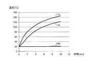
<熱伝導のシミュレーション結果>
図7は、放熱シートを備えない場合の熱伝導のシミュレーション結果を示すグラフであり、図8は、放熱シートを備える場合の熱伝導のシミュレーション結果を示すグラフである。なお、図7,8において、TIA115の発熱量及び受光素子116の発熱量は共に0.8Wである。<Simulation results of heat conduction>
FIG. 7 is a graph showing a simulation result of heat conduction when the heat dissipation sheet is not provided, and FIG. 8 is a graph showing a simulation result of heat conduction when the heat dissipation sheet is provided. 7 and 8, both the heat generation amount of the
図7に示すように、光モジュール500が放熱シート501を備えない場合は、TIA115及び受光素子116の温度が高温になるとともに、受光素子116の温度と、温度センサ550で測定される温度との差が約100℃と大きくなる。 As shown in FIG. 7, when the
これに対し、光モジュール500が放熱シート501を備える場合は、図8に示すように、TIA115及び受光素子116の温度が図7に比べ約100℃低下する。また、TIA115の温度と受光素子116の温度との差が10℃程度であるのに対し、受光素子116の温度と、温度センサ550で測定される温度との差が3℃未満と小さくなる。つまり、放熱シート501を、温度センサ550と受光素子116とに密着するように配置することで、受光素子116の正確な温度を測定することができる。よって、温度に応じた正確な制御が可能になる。 On the other hand, when the
なお、実施例1−4のいずれかの構成に温度センサを適用して放熱シートと温度センサとを密着させてもよい。 In addition, you may apply a temperature sensor to either structure of Example 1-4, and may closely_contact | adhere a thermal radiation sheet | seat and a temperature sensor.
100,200,300,400,500 光モジュール
101 上カバー
101−1 突起
102 下カバー
102−1 突起
111 プリント基板
112 FPC
113 駆動IC
114 発光素子
115 TIA
116 受光素子
120 電気コネクタ
130 光導波路
140,201,202,501 放熱シート
301 金属板
401 弾性体100, 200, 300, 400, 500
113 Drive IC
114
116
Claims (4)
Translated fromJapanese電気信号が伝送される配線パターンを有する第1の回路基板と、
前記電気信号と光との変換を行う光素子が搭載され、前記第1の回路基板に設けられたコネクタに接続されるフレキシブル回路基板と、
前記フレキシブル回路基板の下面側に設けられ、前記光素子から出力される光、または、前記光素子へと入射する光を導波させるシート状の光導波路と、
可塑性を有する第1の熱伝導部材と、
可塑性を有する第2の熱伝導部材と、を備え、
前記筐体内において、
前記第1の回路基板上に、前記光導波路、前記フレキシブル回路基板、前記第1の熱伝導部材の順に積層され、
前記上カバーに形成された第1の突起の下面と、前記第1の熱伝導部材の上面とが密着し、
前記光素子及び前記フレキシブル回路基板を覆うようにして、前記第1の熱伝導部材の下面と前記光素子の上面とが密着し、
前記第1の回路基板と前記光導波路との間に、前記第2の熱伝導部材が積層され、
前記下カバーは、前記第1の突起に対向する位置に形成された第2の突起を有し、
前記第2の突起は、前記第1の回路基板を下方から支持し、
前記第2の突起の上面の面積は、前記第1の突起の下面の面積より小さく、
前記第1の熱伝導部材の厚さが、前記第2の熱伝導部材の厚さより薄い、
ことを特徴とする光モジュール。An upper cover and a lower cover that form a pair of housings;
A first circuit board having a wiring pattern through which an electrical signal is transmitted;
An optical element that converts the electrical signal and light is mounted, anda flexible circuit boardconnected to a connector provided on the first circuit board;
Asheet-like optical waveguide that is provided on the lower surface side of theflexible circuit board and guides light output from the optical element or light incident on the optical element;
A first heat conducting member having plasticity;
A second heat conducting member having plasticity ,
In the housing,
On the first circuit board, the optical waveguide, theflexible circuit board, and the first heat conducting memberare laminated in thisorder ,
The lower surface of the first protrusion formed on the upper cover and the upper surface of the first heat conducting member are in close contact with each other,
The lower surface of the first heat conducting member and the upper surface of the optical element are in close contactso as to cover the optical element and the flexible circuit board ,
The second heat conducting member is laminated between the first circuit board and the optical waveguide,
The lower cover has a second protrusion formed at a position facing the first protrusion,
The second protrusion supports the first circuit board from below,
The area of the upper surface of the second protrusion israther smaller than the area of the lower surface of the first protrusion,
A thickness of the first heat conducting member is less than a thickness of the second heat conducting member;
An optical module characterized by that.
をさらに備えることを特徴とする請求項1に記載の光モジュール。A metal plate laminated between the second heat conducting member and the optical waveguide;
The optical module according to claim1 , further comprising:
をさらに備えることを特徴とする請求項1に記載の光モジュール。An elastic body laminated between the first circuit board and the optical waveguide;
The optical module according to claim 1, further comprising:
前記第1の熱伝導部材と前記温度センサとが密着する、
ことを特徴とする請求項1に記載の光モジュール。A temperature sensor disposed on the first circuit board,
The first heat conducting member and the temperature sensor are in close contact with each other;
The optical module according to claim 1.
Priority Applications (2)
| Application Number | Priority Date | Filing Date | Title |
|---|---|---|---|
| JP2013149822AJP6345917B2 (en) | 2013-07-18 | 2013-07-18 | Optical module |
| US14/330,159US9470861B2 (en) | 2013-07-18 | 2014-07-14 | Optical module |
Applications Claiming Priority (1)
| Application Number | Priority Date | Filing Date | Title |
|---|---|---|---|
| JP2013149822AJP6345917B2 (en) | 2013-07-18 | 2013-07-18 | Optical module |
Publications (2)
| Publication Number | Publication Date |
|---|---|
| JP2015022129A JP2015022129A (en) | 2015-02-02 |
| JP6345917B2true JP6345917B2 (en) | 2018-06-20 |
Family
ID=52486637
Family Applications (1)
| Application Number | Title | Priority Date | Filing Date |
|---|---|---|---|
| JP2013149822AExpired - Fee RelatedJP6345917B2 (en) | 2013-07-18 | 2013-07-18 | Optical module |
Country Status (2)
| Country | Link |
|---|---|
| US (1) | US9470861B2 (en) |
| JP (1) | JP6345917B2 (en) |
Families Citing this family (21)
| Publication number | Priority date | Publication date | Assignee | Title |
|---|---|---|---|---|
| JP6459615B2 (en)* | 2015-02-24 | 2019-01-30 | 住友電気工業株式会社 | Optical data link |
| JP2016164634A (en) | 2015-03-06 | 2016-09-08 | 富士通コンポーネント株式会社 | Optical connector |
| EP3121630B1 (en)* | 2015-07-21 | 2023-04-05 | Tyco Electronics Svenska Holdings AB | Optoelectronic module with improved heat management |
| JP2017068206A (en)* | 2015-10-02 | 2017-04-06 | 富士通株式会社 | Optical module |
| EP3258301B1 (en)* | 2016-06-15 | 2020-03-18 | Hisense Broadband Multimedia Technologies, Ltd. | Optical module with status indicator |
| US10012809B2 (en)* | 2016-06-20 | 2018-07-03 | Mellanox Technologies, Ltd. | Printed circuit board assembly with a photonic integrated circuit for an electro-optical interface |
| JP2018097263A (en)* | 2016-12-15 | 2018-06-21 | 富士通コンポーネント株式会社 | Optical module |
| JP2018146723A (en)* | 2017-03-03 | 2018-09-20 | 富士通コンポーネント株式会社 | Optical module |
| JP6564418B2 (en)* | 2017-04-20 | 2019-08-21 | ファナック株式会社 | Optical power monitor device and laser device |
| JP2019067790A (en)* | 2017-09-28 | 2019-04-25 | 富士通コンポーネント株式会社 | Optical module |
| JP2019125662A (en)* | 2018-01-16 | 2019-07-25 | 富士通コンポーネント株式会社 | High frequency module |
| CN114035282B (en)* | 2018-08-27 | 2023-03-28 | 苏州旭创科技有限公司 | Optical module |
| JP7359579B2 (en)* | 2019-07-05 | 2023-10-11 | 日東電工株式会社 | Optical and electrical composite transmission module |
| JP7477310B2 (en)* | 2020-01-23 | 2024-05-01 | 日東電工株式会社 | Photoelectric conversion module |
| KR20220131256A (en)* | 2020-02-12 | 2022-09-27 | 닛토덴코 가부시키가이샤 | Optoelectric hybrid substrate and optoelectric composite transmission module |
| JP7681567B2 (en)* | 2020-03-19 | 2025-05-22 | 日東電工株式会社 | Optical and electrical transmission composite module |
| CN216772046U (en)* | 2021-11-19 | 2022-06-17 | 东莞立讯技术有限公司 | Photoelectric connector |
| CN115308854B (en)* | 2022-08-04 | 2023-10-13 | Nano科技(北京)有限公司 | High-integration packaging light engine |
| CN117666041A (en)* | 2022-08-25 | 2024-03-08 | 宁波环球广电科技有限公司 | Optical transceiver module |
| KR20240146554A (en) | 2023-03-29 | 2024-10-08 | 닛토덴코 가부시키가이샤 | Photoelectric composite transmission module and optical communication cable using photoelectric composite transmission module |
| CN117055177A (en)* | 2023-08-03 | 2023-11-14 | 江苏奥雷光电有限公司 | Heat dissipation design method for high-speed high-power optical module |
Family Cites Families (21)
| Publication number | Priority date | Publication date | Assignee | Title |
|---|---|---|---|---|
| JPH02148780A (en)* | 1988-11-29 | 1990-06-07 | Hitachi Eng Co Ltd | Temperature stabilization method for semiconductor laser devices |
| JP2916626B2 (en)* | 1989-08-31 | 1999-07-05 | 株式会社光電製作所 | Forced cooling laser pulse generator |
| JPH07302949A (en)* | 1994-05-02 | 1995-11-14 | Olympus Optical Co Ltd | Wavelength stabilizing device |
| US6851869B2 (en)* | 2000-08-04 | 2005-02-08 | Cool Options, Inc. | Highly thermally conductive electronic connector |
| JP2003224386A (en)* | 2002-01-31 | 2003-08-08 | Toyota Motor Corp | Automotive electronic device and automotive electronic device housing |
| US6749345B1 (en)* | 2002-05-24 | 2004-06-15 | National Semiconductor Corporation | Apparatus and method for electro-optical packages that facilitate the coupling of optical cables to printed circuit boards |
| US7228020B2 (en)* | 2004-08-31 | 2007-06-05 | Finisar Corporation | Optoelectronic arrangement having a surface-mountable semiconductor module and a cooling element |
| JP2007079283A (en)* | 2005-09-15 | 2007-03-29 | Sony Corp | Optical integrated circuit |
| WO2007063813A1 (en)* | 2005-12-02 | 2007-06-07 | Kyocera Corporation | Optical waveguide member, optical wiring board, optical wiring module and method for manufacturing optical waveguide member and optical wiring board |
| JP2007271998A (en)* | 2006-03-31 | 2007-10-18 | Nec Corp | Optical connector and optical module |
| US7881059B2 (en)* | 2008-01-29 | 2011-02-01 | Finisar Corporation | Heat management in an electronic module |
| JP2009218299A (en)* | 2008-03-07 | 2009-09-24 | Nec Corp | Liquid cooling module |
| JP5182166B2 (en)* | 2009-03-12 | 2013-04-10 | 日立電線株式会社 | Optical transceiver |
| US8290008B2 (en)* | 2009-08-20 | 2012-10-16 | International Business Machines Corporation | Silicon carrier optoelectronic packaging |
| US20110243509A1 (en)* | 2010-04-05 | 2011-10-06 | Avago Technologies Fiber Ip (Singapore) Pte. Ltd. | Opto-electronic transceiver module system |
| GB201012829D0 (en)* | 2010-07-30 | 2010-09-15 | Oclaro Technology Ltd | Enclosure for a laser package and laser package comprising same |
| JP5779855B2 (en) | 2010-09-24 | 2015-09-16 | 富士通株式会社 | Optical module and manufacturing method |
| US8644712B2 (en)* | 2011-06-23 | 2014-02-04 | Avago Technologies General Ip (Singapore) Pte. Ltd. | Opto-electronic transceiver module with housing having thermally conductive protrusion |
| JP5708816B2 (en)* | 2011-09-29 | 2015-04-30 | 富士通株式会社 | Optical module |
| EP2605345B1 (en)* | 2011-12-13 | 2021-04-28 | Alcatel Lucent | Thermal management of photonics assemblies |
| JP5314119B2 (en)* | 2011-12-26 | 2013-10-16 | 株式会社フジクラ | Optical module |
- 2013
- 2013-07-18JPJP2013149822Apatent/JP6345917B2/ennot_activeExpired - Fee Related
- 2014
- 2014-07-14USUS14/330,159patent/US9470861B2/ennot_activeExpired - Fee Related
Also Published As
| Publication number | Publication date |
|---|---|
| US20150331208A1 (en) | 2015-11-19 |
| JP2015022129A (en) | 2015-02-02 |
| US9470861B2 (en) | 2016-10-18 |
Similar Documents
| Publication | Publication Date | Title |
|---|---|---|
| JP6345917B2 (en) | Optical module | |
| JP7006383B2 (en) | Optical transceiver | |
| JP2015023143A (en) | Optical module | |
| JP4743107B2 (en) | Photoelectric wiring member | |
| US9325418B2 (en) | Optical module with flexible wiring board | |
| JP5371106B2 (en) | Heat dissipation structure for image sensor package | |
| JP5533431B2 (en) | Optical module | |
| US6894903B2 (en) | Optical data link | |
| CN109287131A (en) | Optoelectronic module assembly and method of manufacture | |
| JP5323518B2 (en) | Parallel optical transmission equipment | |
| CN110927894B (en) | optical transceiver | |
| US10386592B2 (en) | Optical engine and optical module | |
| JP6155531B2 (en) | Optical communication module | |
| JP2012069882A (en) | Optical module | |
| JP4856028B2 (en) | Optical module | |
| EP1237025A2 (en) | Opto-electronic module with printed circuit board (PCB) | |
| JP4935936B2 (en) | Photoelectric wiring member | |
| KR100575639B1 (en) | Module for heatsink and PC integrated optical storage device | |
| TWI896588B (en) | Photoelectric conversion module | |
| JP2008066362A (en) | Optical transmission module | |
| JP5047388B2 (en) | Optical module | |
| CN115053160A (en) | Opto-electric hybrid board and opto-electric composite transmission module | |
| JP2011151327A (en) | Optical module, and method of manufacturing the same | |
| CN118610889A (en) | VCSEL array, VCSEL laser and preparation method thereof | |
| CN118738946A (en) | Optoelectronic composite transmission module and optical communication cable using the same |
Legal Events
| Date | Code | Title | Description |
|---|---|---|---|
| A621 | Written request for application examination | Free format text:JAPANESE INTERMEDIATE CODE: A621 Effective date:20160601 | |
| A977 | Report on retrieval | Free format text:JAPANESE INTERMEDIATE CODE: A971007 Effective date:20170315 | |
| A131 | Notification of reasons for refusal | Free format text:JAPANESE INTERMEDIATE CODE: A131 Effective date:20170328 | |
| A521 | Request for written amendment filed | Free format text:JAPANESE INTERMEDIATE CODE: A523 Effective date:20170529 | |
| A131 | Notification of reasons for refusal | Free format text:JAPANESE INTERMEDIATE CODE: A131 Effective date:20171017 | |
| A521 | Request for written amendment filed | Free format text:JAPANESE INTERMEDIATE CODE: A523 Effective date:20171218 | |
| TRDD | Decision of grant or rejection written | ||
| A01 | Written decision to grant a patent or to grant a registration (utility model) | Free format text:JAPANESE INTERMEDIATE CODE: A01 Effective date:20180515 | |
| A61 | First payment of annual fees (during grant procedure) | Free format text:JAPANESE INTERMEDIATE CODE: A61 Effective date:20180524 | |
| R150 | Certificate of patent or registration of utility model | Ref document number:6345917 Country of ref document:JP Free format text:JAPANESE INTERMEDIATE CODE: R150 | |
| LAPS | Cancellation because of no payment of annual fees |