JP6331809B2 - Electronic component conveying device and electronic component inspection device - Google Patents
Electronic component conveying device and electronic component inspection deviceDownload PDFInfo
- Publication number
- JP6331809B2 JP6331809B2JP2014146841AJP2014146841AJP6331809B2JP 6331809 B2JP6331809 B2JP 6331809B2JP 2014146841 AJP2014146841 AJP 2014146841AJP 2014146841 AJP2014146841 AJP 2014146841AJP 6331809 B2JP6331809 B2JP 6331809B2
- Authority
- JP
- Japan
- Prior art keywords
- electronic component
- unit
- light
- mounting plate
- reflection
- Prior art date
- Legal status (The legal status is an assumption and is not a legal conclusion. Google has not performed a legal analysis and makes no representation as to the accuracy of the status listed.)
- Expired - Fee Related
Links
- 238000007689inspectionMethods0.000titleclaimsdescription66
- 230000032258transportEffects0.000claimsdescription52
- 238000001514detection methodMethods0.000claimsdescription28
- 230000010287polarizationEffects0.000claimsdescription8
- 238000011084recoveryMethods0.000description29
- 230000007723transport mechanismEffects0.000description14
- 238000000034methodMethods0.000description10
- 230000007246mechanismEffects0.000description8
- 230000005540biological transmissionEffects0.000description5
- 238000004519manufacturing processMethods0.000description4
- 239000000523sampleSubstances0.000description4
- 238000012360testing methodMethods0.000description4
- 238000010586diagramMethods0.000description3
- 239000000853adhesiveSubstances0.000description2
- 239000002390adhesive tapeSubstances0.000description2
- 229910052782aluminiumInorganic materials0.000description2
- XAGFODPZIPBFFR-UHFFFAOYSA-NaluminiumChemical compound[Al]XAGFODPZIPBFFR-UHFFFAOYSA-N0.000description2
- 239000011159matrix materialSubstances0.000description2
- 238000011144upstream manufacturingMethods0.000description2
- ZCDOYSPFYFSLEW-UHFFFAOYSA-Nchromate(2-)Chemical compound[O-][Cr]([O-])(=O)=OZCDOYSPFYFSLEW-UHFFFAOYSA-N0.000description1
- 239000011248coating agentSubstances0.000description1
- 238000000576coating methodMethods0.000description1
- 239000000470constituentSubstances0.000description1
- 238000009792diffusion processMethods0.000description1
- 230000006870functionEffects0.000description1
- 239000004973liquid crystal related substanceSubstances0.000description1
- 239000000463materialSubstances0.000description1
- 239000012528membraneSubstances0.000description1
- 239000007769metal materialSubstances0.000description1
- 239000002245particleSubstances0.000description1
- 230000011514reflexEffects0.000description1
- 235000012431wafersNutrition0.000description1
Images


Landscapes
- Testing Of Individual Semiconductor Devices (AREA)
- Container, Conveyance, Adherence, Positioning, Of Wafer (AREA)
Description
Translated fromJapanese本発明は、電子部品搬送装置および電子部品検査装置に関する。 The present invention relates to an electronic component conveying device and an electronic component inspection device.
従来、電子部品やウェハー等の種々の部品を製造する製造装置では、当該部品の種類を判別する判別センサーが用いられることが知られている。 Conventionally, it is known that in a manufacturing apparatus for manufacturing various parts such as electronic parts and wafers, a discrimination sensor for discriminating the type of the part is used.
例えば、特許文献1では、判別センサーは、光を発光する発光素子と、発光素子とは別体で構成され、発光素子からの光が部品で反射した反射光を受光する受光素子とを備えている。 For example, in Patent Document 1, the discrimination sensor includes a light emitting element that emits light and a light receiving element that is configured separately from the light emitting element and that receives reflected light that is reflected from the light from the light emitting element. Yes.
しかしながら、特許文献1に記載の発明では、発光素子と受光素子とは、製造装置内で適切な(投受光可能な)位置関係をもって配置する必要があり、そのため、互いに十分に離間させて配置させる必要があった。従って、発光素子と受光素子と十分に離間させた分、部品を判別するための領域を広く確保しなければならないという問題があった。 However, in the invention described in Patent Document 1, it is necessary to arrange the light emitting element and the light receiving element with an appropriate positional relationship (allowing light projection and reception) within the manufacturing apparatus. There was a need. Therefore, there has been a problem that a region for discriminating components must be secured as much as the light emitting element and the light receiving element are sufficiently separated from each other.
また、発光素子と受光素子と互いに対向配置させて、透過型センサーとして用いた場合、発光素子からの光が受光素子まで到達するように、例えば、部品を載置する載置治具や、その他に当該治具を支持する支持部材等に光透過用の貫通孔を設ける必要がある。そのため、製造装置の構成が複雑化するという問題があった。 In addition, when the light-emitting element and the light-receiving element are arranged to face each other and used as a transmission type sensor, for example, a mounting jig for mounting components or the like so that the light from the light-emitting element reaches the light-receiving element It is necessary to provide a through hole for transmitting light in a support member or the like that supports the jig. Therefore, there is a problem that the configuration of the manufacturing apparatus becomes complicated.
本発明の目的は、電子部品配置部上の電子部品の有無を判断する領域での省スペース化に優れ、構成が簡単な電子部品搬送装置および電子部品検査装置を提供することにある。 An object of the present invention is to provide an electronic component transport apparatus and an electronic component inspection apparatus that are excellent in space saving in an area for determining the presence or absence of an electronic component on an electronic component placement unit and that have a simple configuration.
このような目的は、下記の本発明により達成される。
[適用例1]
本発明の電子部品搬送装置は、2つの領域間を移動可能な移動部と、
前記移動部に載置可能で、前記移動部に載置された状態で前記移動部とともに移動し、電子部品を配置する電子部品配置部と、
前記2つの領域のうちの一方の領域内に固定して設けられており、光を発光する発光部と、前記光を受光可能な受光部とを備え、前記受光した光に基づいて、前記一方の領域内で、前記電子部品配置部上の前記電子部品の有無を判断する検出部と、
前記移動部に設けられ、前記光を反射する反射部と、を備え、
前記電子部品配置部は、板状部材で構成されたものであり、前記板状部材の上面に開口して形成され、前記電子部品が収納される少なくとも1つの凹部と、前記凹部の底部に貫通して形成された貫通孔とを有し、
前記移動部は、前記電子部品配置部が載置される載置板と、前記載置板を移動可能に支持する支持部とを有し、
前記反射部は、前記載置板に対して固定され、前記載置板と、前記載置板に載置された前記電子部品配置部との間に配置された膜状または板状をなす部材で構成され、平面視で前記貫通孔と重なっていることを特徴とする。Such an object is achieved by the present invention described below.
[Application Example 1]
The electronic component transport device of the present invention includes a moving unit that can movebetween two regions ,
An electronic component placement unit that can beplaced on the moving unit, moves with the moving unit in a state of being placed on the moving unit, and places an electronic component;
The two fixed to one of the regions is provided within the region, and a light emitting portion for emitting light, and a said lightcapable of receivinga light receiving unit, based on the receivedlight, the one In the region, a detection unit for determining the presence or absence of the electronic componenton the electronic component placement unit ,
A reflection unit provided in the moving unit and reflecting the light;
The electronic component placement portion is composed of a plate-like member, and is formed to open at the upper surface of the plate-like member, and penetrates at least one concave portion in which the electronic component is accommodated, and the bottom portion of the concave portion. And a through hole formed as
The moving unit includes a mounting plate on which the electronic component placement unit is mounted, and a support unit that supports the mounting plate to be movable.
The reflection portion is fixed to the mounting plate, and is a film-like or plate-like member disposed between the mounting plate and the electronic component placement portion placed on the mounting plate. It overlaps with the said through-hole by planar view, It is characterized by the above-mentioned.
これにより、電子部品配置部上の電子部品の有無を判断する領域で、検出部と反射部とをできる限り近づけて集約的に配置することができる。よって、当該領域での省スペース化に優れる。また、検出部に発光部と受光部とが一体化された反射型のものを用いているため、透過型のものを用いた場合に比べて当該領域での構成が簡単となる。 Thereby, in the area | region which judges the presence or absence of the electronic component on an electronic component arrangement | positioning part, a detection part and a reflection part can be arrange | positioned collectively as closely as possible. Therefore, it is excellent in space saving in the area. In addition, since a reflective type in which the light emitting unit and the light receiving unit are integrated is used as the detection unit, the configuration in the region is simpler than when a transmission type is used.
[適用例2]
本発明の電子部品搬送装置では、前記発光部から前記光を発光した際、前記光は、前記電子部品が前記凹部に収納されている場合には、前記電子部品で遮光され、前記反射部には至らず、前記電子部品が前記凹部に収納されていない場合には、前記貫通孔を通過して、前記反射部に至るのが好ましい。[Application Example 2]
In the electronic component transport device according to the aspect of theinvention, when the light is emitted from the light emitting unit, the light is shielded by the electronic component when the electronic component is stored in the recess, and is reflected on the reflecting unit. not enough, when said electronic part is not accommodated in said recess, through said through hole,not the preferred fromreaching the reflectiveportion.
[適用例3]
本発明の電子部品搬送装置では、前記載置板は、上面に開口して形成され、前記反射部が収納される反射部収納用凹部を有し、
前記反射部収納用凹部の深さは、前記反射部の厚さよりも大きいのが好ましい。[Application Example 3]
In the electronic component transport device of the present invention, the mountingplate is formed to have an opening on the upper surface, and has a concave portion for storing the reflecting portion in which the reflecting portion is stored,
It is preferable that the depth of the concave portion for storing the reflecting portion is larger than the thickness of the reflecting portion .
[適用例4]
本発明の電子部品搬送装置では、前記電子部品配置部は、前記凹部を複数有し、
前記反射部は、1つの前記膜状または板状をなす部材で構成され、平面視で前記各凹部の底部に形成された前記貫通孔と重なっているのが好ましい。
[適用例5]
本発明の電子部品搬送装置では、前記電子部品配置部は、黒色のものであるのが好ましい。[Application Example 4]
In the electronic component transport device of the present invention, the electronic componentplacement unit has a plurality of the recesses,
It is preferable that the reflection portion is formed of one member having a film shape or a plate shape, and overlaps with the through hole formed in the bottom portion of each concave portion in plan view .
[Application Example 5]
In the electronic component transport device of the present invention, it is preferable that the electronic component placement portion is black.
[適用例6]
本発明の電子部品搬送装置では、前記検出部は、前記受光部が前記反射部で反射した光を受光した場合、前記電子部品が載置されていない、と判断するのが好ましい。[Application Example 6]
In the electronic component transport apparatus according to the aspect of the invention, it is preferable that the detection unit determines that the electronic component is not placed when the light receiving unit receives light reflected by the reflection unit.
これにより、電子部品配置部上の電子部品の有無を判断する際、その判断を正確かつ迅速に行なうことができる。 Thereby, when determining the presence or absence of an electronic component on the electronic component placement unit, the determination can be performed accurately and quickly.
[適用例7]
本発明の電子部品搬送装置では、前記電子部品が載置されていないと判断した場合に、前記電子部品が載置されていない旨を報知する報知部を備えるのが好ましい。
[適用例8]
本発明の電子部品搬送装置では、前記検出部は、前記受光部が前記反射部で反射した光を受光しない場合、前記電子部品が載置されている、と判断するのが好ましい。
[適用例9]
本発明の電子部品搬送装置では、前記電子部品が載置されていると判断した場合に、前記電子部品配置部から前記電子部品を把持し、搬送する搬送部を備えるのが好ましい。
[適用例10]
本発明の電子部品搬送装置では、前記2つの領域のうちの一方の領域内では、前記電子部品に対して少なくとも1つの検査が行なわれ、
前記検出部は、前記検査が終わった後に、前記電子部品の有無を判断するのが好ましい。[Application Example 7]
In the electronic component transport device of the present invention, it is preferable to include a notifying unit that notifies that the electronic component is not placed when it is determined that the electronic component is not placed.
[Application Example 8]
In the electronic component transport device according to the aspect of the invention, it is preferable that the detection unit determines that the electronic component is placed when the light receiving unit does not receive the light reflected by the reflection unit.
[Application Example 9]
In the electronic component transport apparatus according to the present invention, it is preferable to include a transport unit that grips and transports the electronic component from the electronic component placement unit when it is determined that the electronic component is placed.
[Application Example 10]
In the electronic component transport device of the present invention,at least one inspection is performed on the electronic component in one of the two regions.
Wherein the detection unit, before after the end of thedangerous査, preferably to determine the presence or absence of the electronic component.
検査後では、検査結果に応じた分類が多数箇所有する場合がある。この場合、電子部品配置部上の電子部品が無ければ迅速な分類が阻害されるおそれがあるが、分類に先立って電子部品の有無が判断されるため、当該有無に応じた迅速な対応が可能となる。 After the inspection, there may be many classifications according to the inspection result. In this case, if there is no electronic component on the electronic component placement section, there is a risk that rapid classification may be hindered, but since the presence or absence of electronic components is determined prior to classification, it is possible to respond quickly according to the presence or absence It becomes.
[適用例11]
本発明の電子部品搬送装置では、前記反射部が光を反射させる場合、前記反射部へ入射する光の偏光方向と、前記反射部から反射された光の偏光方向は異なるのが好ましい。[Application Example 11]
In the electronic component transport device according to the aspect of the invention, it is preferable that when the reflection unit reflects light, the polarization direction of the light incident on the reflection unit is different from the polarization direction of the light reflected from the reflection unit.
これにより、検出部として回帰反射型のものを用いることができ、よって、反射光の有無に応じて、電子部品の有無の判断を正確に行なうことができる。 As a result, a regression reflection type detector can be used as the detection unit, and therefore the presence / absence of an electronic component can be accurately determined according to the presence / absence of reflected light.
[適用例12]
本発明の電子部品搬送装置では、前記反射部は、接合部材を介して前記移動部に貼り付けられているのが好ましい。[Application Example 12]
In the electronic component transport device according to the aspect of the invention, it is preferable that the reflecting portion is attached to the moving portion via a joining member.
これにより、反射部は、移動部に対して固定されて、当該移動部の移動中に位置ズレが生じるのが防止され、よって、発光部からの光を反射させ得る状態となる。 As a result, the reflecting portion is fixed with respect to the moving portion, so that a positional shift is prevented from occurring during the movement of the moving portion, so that the light from the light emitting portion can be reflected.
[適用例13]
本発明の電子部品検査装置は、2つの領域間を移動可能な移動部と、
前記移動部に載置可能で、前記移動部に載置された状態で前記移動部とともに移動し、電子部品を配置する電子部品配置部と、
前記2つの領域のうちの一方の領域内に固定して設けられており、光を発光する発光部と、前記光を受光可能な受光部とを備え、前記受光した光に基づいて、前記一方の領域内で、前記電子部品配置部上の前記電子部品の有無を判断する検出部と、
前記移動部に設けられ、前記光を反射する反射部と、
前記2つの領域のうちの他方の領域内で前記電子部品を検査する検査部と、を備え、
前記電子部品配置部は、板状部材で構成されたものであり、前記板状部材の上面に開口して形成され、前記電子部品が収納される少なくとも1つの凹部と、前記凹部の底部に貫通して形成された貫通孔とを有し、
前記移動部は、前記電子部品配置部が載置される載置板と、前記載置板を移動可能に支持する支持部とを有し、
前記反射部は、前記載置板に対して固定され、前記載置板と、前記載置板に載置された前記電子部品配置部との間に配置された膜状または板状をなす部材で構成され、平面視で前記貫通孔と重なっていることを特徴とする。[Application Example 13]
The electronic component inspection apparatus of the present invention includes a moving unit that can movebetween two regions ,
An electronic component placement unit that can beplaced on the moving unit, moves with the moving unit in a state of being placed on the moving unit, and places an electronic component;
The two fixed to one of the regions is provided within the region, and a light emitting portion for emitting light, and a said lightcapable of receivinga light receiving unit, based on the receivedlight, the one In the region, a detection unit for determining the presence or absence of the electronic componenton the electronic component placement unit ,
A reflecting portion provided in the moving portion and reflecting the light;
An inspection unit for inspecting the electronic componentin the other region of the two regions,
The electronic component placement portion is composed of a plate-like member, and is formed to open at the upper surface of the plate-like member, and penetrates at least one concave portion in which the electronic component is accommodated, and the bottom portion of the concave portion. And a through hole formed as
The moving unit includes a mounting plate on which the electronic component placement unit is mounted, and a support unit that supports the mounting plate to be movable.
The reflection portion is fixed to the mounting plate, and is a film-like or plate-like member disposed between the mounting plate and the electronic component placement portion placed on the mounting plate. It overlaps with the said through-hole by planar view, It is characterized by the above-mentioned.
これにより、電子部品配置部上の電子部品の有無を判断する領域で、検出部と反射部とをできる限り近づけて集約的に配置することができる。よって、当該領域での省スペース化に優れる。また、検出部に発光部と受光部とが一体化された反射型のものを用いているため、透過型のものを用いた場合に比べて当該領域での構成が簡単となる。 Thereby, in the area | region which judges the presence or absence of the electronic component on an electronic component arrangement | positioning part, a detection part and a reflection part can be arrange | positioned collectively as closely as possible. Therefore, it is excellent in space saving in the area. In addition, since a reflective type in which the light emitting unit and the light receiving unit are integrated is used as the detection unit, the configuration in the region is simpler than when a transmission type is used.
以下、本発明の電子部品搬送装置および電子部品検査装置を添付図面に示す好適な実施形態に基づいて詳細に説明する。 DESCRIPTION OF THE PREFERRED EMBODIMENTS Hereinafter, an electronic component conveying device and an electronic component inspection device according to the present invention will be described in detail based on preferred embodiments shown in the accompanying drawings.
図1は、本発明の電子部品検査装置の実施形態を示す概略平面図である。図2、図3は、それぞれ、図1に示す電子部品検査装置が備えるデバイス回収部上のICデバイスの有無を検出するタイミングを説明するための図である。図4、図5は、それぞれ、デバイス回収部と反射部との位置関係を示す平面図である。図6は、ICデバイスの有無を検出するための光の反射状態を示す斜視図である。図7は、図6中の光の反射状態を拡大した拡大詳細図である。図8は、図1に示す電子部品検査装置が備える制御部の制御プログラムを示すフローチャートである。なお、以下では、説明の便宜上、図1に示すように、互いに直交する3軸をX軸(第1軸)、Y軸(第2軸)およびZ軸(第3軸)とする。また、X軸とY軸を含むXY平面が水平となっており、Z軸が鉛直となっている。また、X軸に平行な方向を「X方向」とも言い、Y軸に平行な方向を「Y方向」とも言い、Z軸に平行な方向を「Z方向」とも言う。また、電子部品の搬送方向の上流側を単に「上流側」とも言い、下流側を単に「下流側」とも言う。また、本願明細書で言う「水平」とは、完全な水平に限定されず、電子部品の搬送が阻害されない限り、水平に対して若干(例えば5°未満程度)傾いていた状態も含む。 FIG. 1 is a schematic plan view showing an embodiment of an electronic component inspection apparatus of the present invention. FIG. 2 and FIG. 3 are diagrams for explaining the timing for detecting the presence or absence of an IC device on the device collection unit provided in the electronic component inspection apparatus shown in FIG. 4 and 5 are plan views showing the positional relationship between the device collection unit and the reflection unit, respectively. FIG. 6 is a perspective view showing a light reflection state for detecting the presence or absence of an IC device. FIG. 7 is an enlarged detail view in which the light reflection state in FIG. 6 is enlarged. FIG. 8 is a flowchart showing a control program of a control unit provided in the electronic component inspection apparatus shown in FIG. In the following, for convenience of explanation, as shown in FIG. 1, three axes orthogonal to each other are referred to as an X axis (first axis), a Y axis (second axis), and a Z axis (third axis). Further, the XY plane including the X axis and the Y axis is horizontal, and the Z axis is vertical. A direction parallel to the X axis is also referred to as “X direction”, a direction parallel to the Y axis is also referred to as “Y direction”, and a direction parallel to the Z axis is also referred to as “Z direction”. Further, the upstream side in the conveying direction of the electronic component is also simply referred to as “upstream side”, and the downstream side is also simply referred to as “downstream side”. In addition, “horizontal” as used in the specification of the present application is not limited to complete horizontal, and includes a state where the electronic component is slightly inclined (for example, less than about 5 °) as long as transportation of electronic components is not hindered.
図1に示す検査装置(電子部品検査装置)1は、例えば、BGA(Ball grid array)パッケージやLGA(Land grid array)パッケージ等のICデバイス、LCD(Liquid Crystal Display)、CIS(CMOS Image Sensor)等の電子部品の電気的特性を検査・試験(以下単に「検査」と言う)するための装置である。なお、以下では、説明の便宜上、検査を行う前記電子部品としてICデバイスを用いる場合について代表して説明し、これを「ICデバイス90」とする。 An inspection apparatus (electronic component inspection apparatus) 1 shown in FIG. 1 includes, for example, an IC device such as a BGA (Ball grid array) package and an LGA (Land grid array) package, an LCD (Liquid Crystal Display), and a CIS (CMOS Image Sensor). It is an apparatus for inspecting and testing (hereinafter simply referred to as “inspection”) electrical characteristics of electronic components such as the above. Hereinafter, for convenience of explanation, the case where an IC device is used as the electronic component to be inspected will be described as a representative, and this will be referred to as “
図1に示すように、検査装置1は、トレイ供給領域A1と、デバイス供給領域(以下単に「供給領域」と言う)A2と、検査領域A3と、デバイス回収領域(以下単に「回収領域」と言う)A4と、トレイ除去領域A5とに分けられている。そして、ICデバイス90は、トレイ供給領域A1からトレイ除去領域A5まで前記各領域を順に経由し、途中の検査領域A3で検査が行われる。このように検査装置1は、各領域でICデバイス90を搬送する電子部品搬送装置と、検査領域A3内で検査を行なう検査部16と、制御部80とを備えたものとなっている。 As shown in FIG. 1, the inspection apparatus 1 includes a tray supply area A1, a device supply area (hereinafter simply referred to as “supply area”) A2, an inspection area A3, and a device collection area (hereinafter simply referred to as “collection area”). Say) A4 and tray removal area A5. Then, the
トレイ供給領域A1は、未検査状態の複数のICデバイス90が配列されたトレイ200が供給される領域である。トレイ供給領域A1では、多数のトレイ200を積み重ねることができる。 The tray supply area A1 is an area to which a
供給領域A2は、トレイ供給領域A1からのトレイ200上に配置された複数のICデバイス90がそれぞれ検査領域A3まで供給される領域である。なお、トレイ供給領域A1と供給領域A2とをまたぐように、トレイ200を1枚ずつ搬送するトレイ搬送機構11A、11Bが設けられている。 The supply area A2 is an area where a plurality of
供給領域A2には、温度調整部(ソークプレート)12と、デバイス搬送ヘッド13と、トレイ搬送機構(第1搬送装置)15とが設けられている。 In the supply area A2, a temperature adjusting unit (soak plate) 12, a
温度調整部12は、複数のICデバイス90を加熱または冷却して、当該ICデバイス90を検査に適した温度に調整する装置である。図1に示す構成では、温度調整部12は、Y方向に2つ配置、固定されている。そして、トレイ搬送機構11Aによってトレイ供給領域A1から搬入された(搬送されてきた)トレイ200上のICデバイス90は、いずれかの温度調整部12に搬送され、載置される。 The temperature adjustment unit 12 is an apparatus that heats or cools the plurality of
デバイス搬送ヘッド13は、供給領域A2内で移動可能に支持されている。これにより、デバイス搬送ヘッド13は、トレイ供給領域A1から搬入されたトレイ200と温度調整部12との間のICデバイス90の搬送と、温度調整部12と後述するデバイス供給部14との間のICデバイス90の搬送とを担うことができる。 The
トレイ搬送機構15は、全てのICデバイス90が除去された状態の空のトレイ200をX方向に搬送させる機構である。そして、この搬送後、空のトレイ200は、トレイ搬送機構11Bによって供給領域A2からトレイ供給領域A1に戻される。 The
検査領域A3は、ICデバイス90を検査する領域である。この検査領域A3には、デバイス供給部(供給シャトル)14と、検査部16と、デバイス搬送ヘッド17と、デバイス回収部(回収シャトル)18とが設けられている。 The inspection area A3 is an area where the
デバイス供給部14は、温度調整されたICデバイス90を検査部16近傍まで搬送する装置である。このデバイス供給部14は、供給領域A2と検査領域A3との間をX方向に沿って移動可能に支持されている。また、図1に示す構成では、デバイス供給部14は、Y方向に2つ配置されており、温度調整部12上のICデバイス90は、いずれかのデバイス供給部14に搬送され、載置される。 The
検査部16は、ICデバイス90の電気的特性を検査・試験するユニットである。検査部16には、ICデバイス90を保持した状態で当該ICデバイス90の端子と電気的に接続される複数のプローブピンが設けられている。各プローブピンは、、検査部16に接続されるテスターが備える検査回路部に電気的に接続されている。そして、ICデバイス90の端子とプローブピンとが電気的に接続され(接触し)、プローブピンを介してICデバイス90の検査が行われる。ICデバイス90の検査は、前記検査制御部に記憶されているプログラムに基づいて行われる。なお、検査部16では、温度調整部12と同様に、ICデバイス90を加熱または冷却して、当該ICデバイス90を検査に適した温度に制御することができる。 The
デバイス搬送ヘッド17は、検査領域A3内で移動可能に支持されている。これにより、デバイス搬送ヘッド17は、供給領域A2から搬入されたデバイス供給部14上のICデバイス90を検査部16上に搬送し、載置することができる。 The device transport head 17 is supported so as to be movable in the inspection area A3. Thereby, the device transport head 17 can transport and place the
デバイス回収部18は、検査部16での検査が終了したICデバイス90を回収領域A4まで搬送する回収する装置である。このデバイス回収部18は、検査領域A3と回収領域A4との間をX方向に沿って移動可能に支持されている。また、図1に示す構成では、デバイス回収部18は、デバイス供給部14と同様に、Y方向に2つ配置されており、検査部16上のICデバイス90は、いずれかのデバイス回収部18に搬送され、載置される。この搬送は、デバイス搬送ヘッド17によって行なわれる。 The
回収領域A4は、検査が終了したICデバイス90が回収される領域である。この回収領域A4には、回収用トレイ19と、デバイス搬送ヘッド20と、トレイ搬送機構21とが設けられている。また、回収領域A4には、空のトレイ200も用意されている。 The collection area A4 is an area where the
回収用トレイ19は、回収領域A4内に固定され、図1に示す構成では、X方向に沿って3つ配置されている。また、空のトレイ200も、X方向に沿って3つ配置されている。そして、回収領域A4に移動してきたデバイス回収部18上のICデバイス90は、これらの回収用トレイ19および空のトレイ200のうちのいずれかに搬送され、載置される。これにより、ICデバイス90は、検査結果ごとに回収されて、分類されることとなる。 The
デバイス搬送ヘッド20は、回収領域A4内で移動可能に支持されている。これにより、デバイス搬送ヘッド20は、ICデバイス90をデバイス回収部18から回収用トレイ19や空のトレイ200に搬送することができる。 The device transport head 20 is supported so as to be movable in the collection area A4. Accordingly, the device transport head 20 can transport the
トレイ搬送機構21は、トレイ除去領域A5から搬入された空のトレイ200をX方向に搬送させる機構である。そして、この搬送後、空のトレイ200は、ICデバイス90が回収される位置に配されることとなる、すなわち、前記3つの空のトレイ200のうちのいずれかとなり得る。 The
トレイ除去領域A5は、検査済み状態の複数のICデバイス90が配列されたトレイ200が回収され、除去される領域である。トレイ除去領域A5では、多数のトレイ200を積み重ねることができる。 The tray removal area A5 is an area where the
また、回収領域A4とトレイ除去領域A5とをまたぐように、トレイ200を1枚ずつ搬送するトレイ搬送機構22A、22Bが設けられている。トレイ搬送機構22Aは、検査済みのICデバイス90が載置されたトレイ200を回収領域A4からトレイ除去領域A5に搬送する機構である。トレイ搬送機構22Bは、ICデバイス90を回収するための空のトレイ200をトレイ除去領域A5から回収領域A4に搬送する機構である。 In addition,
制御部80は、例えば、駆動制御部を有している。駆動制御部は、例えば、トレイ搬送機構11A、11Bと、温度調整部12と、デバイス搬送ヘッド13と、デバイス供給部14と、トレイ搬送機構15と、検査部16と、デバイス搬送ヘッド17と、デバイス回収部18と、デバイス搬送ヘッド20と、トレイ搬送機構21と、トレイ搬送機構22A、22Bの各部の駆動を制御する。 The
なお、前記テスターの検査制御部は、例えば、図示しないメモリー内に記憶されたプログラムに基づいて、検査部16に配置されたICデバイス90の電気的特性の検査等を行なう。 The test control unit of the tester inspects the electrical characteristics of the
検査装置1では、回収領域A4でICデバイス90をデバイス回収部18から回収用トレイ19に搬送する際、その搬送をデバイス搬送ヘッド20が担っている。この場合、デバイス回収部18上にICデバイス90が存在していれば、デバイス搬送ヘッド20をICデバイス90に向かわせるが、存在していないならば、デバイス搬送ヘッド20を一旦停止させる、すなわち、待機させるのが好ましい。 In the inspection apparatus 1, when the
以下、デバイス回収部18上のICデバイス90の有無を判断するための構成について説明する。ここでは、回収領域A4に適用した場合を一例として代表的に説明するが、回収領域A4の他に、供給領域A2や検査領域A3でも適用可能である。 Hereinafter, a configuration for determining the presence or absence of the
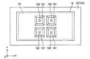
図2、図3に示すように、デバイス回収部18は、板状をなし、ICデバイス90を配置する電子部品配置部であり、上面に開口する少なくとも1つの凹部(ポケット)181を有している。この凹部181には、ICデバイス90を配置、収納することができる。なお、凹部181が複数形成されている場合、凹部181の配置として、例えば図4や図5に示す配置が挙げられる。図4に示すデバイス回収部18は、X方向に沿って2行、Y方向に沿って2列の行列状に配置された4つの凹部181を有している。図5に示すデバイス回収部18は、X方向に沿って4行、Y方向に沿って2列の行列状に配置された8つの凹部181を有している。 As shown in FIGS. 2 and 3, the
また、凹部181の底部には、その中心部に当該底部を貫通する貫通孔182が形成されている。後述するように、貫通孔182は、出射光L1が透過可能な透過孔となっている(図3参照)。貫通孔182の平面形状は、本実施形態では円形となっているが、これに限定されず、例えば、多角形であってもよい。 In addition, a through
デバイス回収部18の構成材料としては、特に限定されず、例えば、アルミニウム等の金属材料を用いることができる。デバイス回収部18がアルミニウムで構成されている場合、デバイス回収部18に黒色クロメート処理を施すのが好ましい。これにより、デバイス回収部18は、黒色のものとなり、当該デバイス回収部18での光の反射(拡散)を抑制または防止することができる。 The constituent material of the
図2、図3に示すように、デバイス回収部18は、X方向に沿って移動可能な移動部23に着脱自在に載置可能となっている。これにより、デバイス回収部18は、移動部23に載置された載置状態で移動部23とともにX方向に沿って移動することができ、よって、検査領域A3と回収領域A4との間を往復することができる。そして、回収領域A4では、デバイス回収部18上のICデバイス90の有無が判断される。 As shown in FIGS. 2 and 3, the
移動部23の構成としては、例えば、デバイス回収部18が載置される載置板231と、載置板231を移動可能に支持するリニアガイド232と、駆動源(図示せず)としてのモーターおよびボールネジとを有するものとすることができる。 As the configuration of the moving
ICデバイス90の有無を判断する検出部24は、回収領域A4内に移動したデバイス回収部18のZ軸正側に配置されている。この検出部24は、デバイス回収部18の凹部181に向けて出射光L1を出射する(発光する)発光部241と、出射光L1が反射部25で反射した反射光L2を受光する受光部242とを備えている。検出部24では、発光部241と受光部242とが隣接して配置され、ユニット化(一体化)されており、いわゆる「反射型」の光電センサーとなっている。 The
図7に示すように、検出部24は、発光部241側に配置された偏光フィルター243と、受光部242側に配置された偏光フィルター244とを備えている。偏光フィルター243と、偏光フィルター244とは、互いに偏光方向が異なっている、すなわち、本実施形態では直交している。 As shown in FIG. 7, the
出射光L1は、偏光フィルター243を通過することにより、一方向に振動した直線偏光(例えば縦方向の波)となり、デバイス回収部18に向かう。その後、出射光L1は、反射部25で回帰反射して、反射光L2として受光部242に向かう。反射光L2は、出射光L1と直交する一方向に振動した(例えば横方向の波)直線偏光となっており、偏光フィルター244を通過することができる。そして、検出部24は、反射光L2の有無で、ICデバイス90の有無を正確に判断する(検出する)ことができる。 The outgoing light L <b> 1 passes through the
なお、検出部24としては、発光部241と受光部242とが隣接して同じ方向を向いた図2や図3に示す構成のもの他に、デバイス回収部18の貫通孔182の大きさによっては、同軸回帰反射型のものを用いることもできる。 In addition to the configuration shown in FIG. 2 and FIG. 3 in which the
図2、図3に示すように、反射部25は、表側の面に反射面251を有する膜状形状(または板状)部材であり、移動部23の載置板231に設けられている。載置板231には、その上面に開口する凹部233が形成されており、当該凹部233内に反射部25が収納、配置されている。このような配置と、検出部24として反射型の光電センサーを用いたこととが相まって、反射部25と検出部24とを可能な限り近づけて集約することができる。これにより、回収領域A4での省スペース化に優れる。また、反射部25と検出部24とが近くなった分、ICデバイス90の有無を正確に検出することができ、誤検出が生じるのを防止することができる。 As shown in FIGS. 2 and 3, the reflecting
また、検出部24として、反射型の光電センサーと異なる、発光部241と受光部242とを分散して配置する透過型の光電センサーを用いた場合、回収領域A4内に発光部241と受光部242とを配置するための部材等を別途設置しなければならない。このため、回収領域A4内の構成が複雑なものとなり得る。これに対し、検査装置1では、検出部24に反射型の光電センサーを用いているため、回収領域A4内の構成が簡単なものとなる。 In addition, when a transmission type photoelectric sensor that disperses and arranges the
また、反射部25は、移動部23と、移動部23に装着されたデバイス回収部18との間に配置された状態となっている。これにより、デバイス回収部18で反射部25が保護され、反射部25の破損が防止される。 Further, the
前述したように、反射部25は、載置板231の凹部233内に収納されている。凹部233の深さは、反射部25の厚さよりも大きい。これにより、反射部25の反射面251と、デバイス回収部18の下面183との間には、間隙184が形成される。これにより、移動部23にデバイス回収部18を装着するときに、当該デバイス回収部18の下面183で反射面251に傷をつけてしまうのを防止することができる。 As described above, the reflecting
また、反射部25は、当該反射部25に入射してくる入射光(出射光L1)の偏光方向と異なる偏光方向の光を、反射光L2として受光部242に回帰反射させるよう構成されている。図6に示すように、反射部25の反射面251は、規則的に配列された多数のコーナーキューブ252で構成されている。「コーナーキューブ」とは、3つの平面を互いに直交するように組み合わせたような形状をなす微小な窪みである。これにより、反射部25は、回帰反射させ得るものとなる。なお、図6では、1つのコーナーキューブ252を拡大して代表的に描いている。また、反射部25は、透明な粒子部材を含んでいてもよい。 The
また、反射部25は、その裏側の面が載置板231の凹部233の底部に、例えば粘着テープや接着剤等の接合部材(図示せず)を介して貼り付けられているのが好ましい。これにより、反射部25は、載置板231に対して固定されて、載置板231の移動中に位置ズレが生じるのを防止することができる。よって、反射部25は、回収領域A4で出射光L1を反射させ得る状態となる。なお、反射部25の貼り付け方法としては、特に限定されず、例えば、両面粘着テープを用いた方法、接着剤を用いた方法等が挙げられる。貼り付け方法の他に、ネジ止めによる固定方法を用いてもよい。 Moreover, it is preferable that the back surface of the
図4、図5に示すように、反射部25は、デバイス回収部18の凹部181の配置個数によらず、反射部25の平面視で全ての凹部181と重なる、すなわち、全ての凹部181を一括して包含する程度の大きさとなっている。これにより、凹部181の配置個数が異なるデバイス回収部18ごとに反射部25を交換するのを省略することができる、すなわち、1つの反射部25をそのまま使用することができる。また、凹部181の配置個数の大小にかかわらず、凹部181の貫通孔182を通過した全ての出射光L1を1つの反射部25で反射させることができる。 As shown in FIGS. 4 and 5, the reflecting
次に、デバイス回収部18上のICデバイス90の有無を判断する制御プログラムを図8に示すフローチャートに基づいて説明する。なお、この制御プログラムは、制御部80に予め記憶されている。 Next, a control program for determining the presence or absence of the
検査領域A3から移動してきたデバイス回収部18は、回収領域A4では図2および図3に示すいずれかの状態となっている。この状態では、デバイス回収部18は、検出部24と反射部25との間に配置される。 The
まず、検出部24を作動させて、発光部241から出射光L1を出射させ、受光部242で反射光L2が受光されたか否か、すなわち、受光部242での反射光L2の有無を判断する(ステップS101)。 First, the
ステップS101において反射光L2を受光しなかったと判断されたら、デバイス回収部18上には、ICデバイス90が存在すると判断する(ステップS102、図2参照)。なお、出射光L1は、ICデバイス90で反射されて反射光L2’となるが、当該反射光L2’は、回帰反射された光とはならず、出射光L1と同じ縦方向の波である。このため、受光部242では、横方向の波である反射光L2が受光されなかったと判断されることとなる。 If it is determined in step S101 that the reflected light L2 has not been received, it is determined that the
次いで、デバイス搬送ヘッド20を作動させて、ICデバイス90に向かわせ、当該ICデバイス90を把持し、例えば回収用トレイ19に搬送する(ステップS103)。 Next, the device transport head 20 is operated to face the
一方、ステップS101において反射光L2を受光したと判断されたら、デバイス回収部18上には、ICデバイス90が存在しないと判断する(ステップS104、図3参照)。 On the other hand, if it is determined in step S101 that the reflected light L2 has been received, it is determined that the
次いで、デバイス回収部18上にICデバイス90が存在しない旨を報知する(ステップS105)。この報知方法としては、特に限定されず、例えば、画像表示による方法、音声による方法、発光による方法等を用いることができる。 Next, it notifies that there is no
また、ステップS105を実行するときは、デバイス搬送ヘッド20を一旦停止させて待機させるのが好ましい。 In addition, when executing Step S105, it is preferable to temporarily stop the device transport head 20 and wait.
また、本実施形態では、ICデバイス90の有無の判断は、当該ICデバイス90に対する検査後に適用している。検査後では、検査結果に応じた分類が多数箇所(図1に示す構成では6つ)有する場合がある。この場合、デバイス回収部18上のICデバイス90が無ければ迅速な分類が阻害されるおそれがあるが、分類に先立ってICデバイス90の有無が判断されるため、当該有無に応じた迅速な対応が可能となる。 In the present embodiment, the determination of the presence or absence of the
以上、本発明の電子部品搬送装置および電子部品検査装置を図示の実施形態について説明したが、本発明は、これに限定されるものではなく、電子部品搬送装置および電子部品検査装置を構成する各部は、同様の機能を発揮し得る任意の構成のものと置換することができる。また、任意の構成物が付加されていてもよい。 As mentioned above, although the electronic component conveyance apparatus and electronic component inspection apparatus of this invention were demonstrated about embodiment of illustration, this invention is not limited to this, Each part which comprises an electronic component conveyance apparatus and an electronic component inspection apparatus Can be replaced with any structure capable of performing the same function. Moreover, arbitrary components may be added.
また、反射部は、前記実施形態では膜状または板状をなす硬質の部材で構成されているが、これに限定されず、塗膜で構成されていてもよい。 Moreover, although the reflection part is comprised with the hard member which makes a film | membrane form or plate shape in the said embodiment, it is not limited to this, You may be comprised with the coating film.
1……検査装置(電子部品検査装置)
11A、11B……トレイ搬送機構
12……温度調整部(ソークプレート)
13……デバイス搬送ヘッド
14……デバイス供給部(供給シャトル)
15……トレイ搬送機構
16……検査部
17……デバイス搬送ヘッド
18……デバイス回収部(回収シャトル)
181……凹部(ポケット)
182……貫通孔
183……下面
184……間隙
19……回収用トレイ
20……デバイス搬送ヘッド
21……トレイ搬送機構
22A、22B……トレイ搬送機構
23……移動部
231……載置板
232……リニアガイド
233……凹部
24……検出部
241……発光部
242……受光部
243……偏光フィルター
244……偏光フィルター
25……反射部
251……反射面
252……コーナーキューブ
80……制御部
90……ICデバイス
200……トレイ
A1……トレイ供給領域
A2……デバイス供給領域(供給領域)
A3……検査領域
A4……デバイス回収領域(回収領域)
A5……トレイ除去領域
L1……出射光
L2、L2’……反射光
S101〜S105……ステップ1 ... Inspection equipment (electronic parts inspection equipment)
11A, 11B ...... Tray transport mechanism 12 ... Temperature adjuster (soak plate)
13 ……
15 ……
181 …… Recess (Pocket)
182 …… Through
A3: Inspection area A4: Device collection area (collection area)
A5 …… Tray removal region L1 …… Exit light L2, L2 ′ …… Reflected light S101 to S105 …… Step
Claims (13)
Translated fromJapanese前記移動部に載置可能で、前記移動部に載置された状態で前記移動部とともに移動し、電子部品を配置する電子部品配置部と、
前記2つの領域のうちの一方の領域内に固定して設けられており、光を発光する発光部と、前記光を受光可能な受光部とを備え、前記受光した光に基づいて、前記一方の領域内で、前記電子部品配置部上の前記電子部品の有無を判断する検出部と、
前記移動部に設けられ、前記光を反射する反射部と、を備え、
前記電子部品配置部は、板状部材で構成されたものであり、前記板状部材の上面に開口して形成され、前記電子部品が収納される少なくとも1つの凹部と、前記凹部の底部に貫通して形成された貫通孔とを有し、
前記移動部は、前記電子部品配置部が載置される載置板と、前記載置板を移動可能に支持する支持部とを有し、
前記反射部は、前記載置板に対して固定され、前記載置板と、前記載置板に載置された前記電子部品配置部との間に配置された膜状または板状をなす部材で構成され、平面視で前記貫通孔と重なっていることを特徴とする電子部品搬送装置。A moving part movablebetween two regions ;
An electronic component placement unit that can beplaced on the moving unit, moves with the moving unit in a state of being placed on the moving unit, and places an electronic component;
The two fixed to one of the regions is provided within the region, and a light emitting portion for emitting light, and a said lightcapable of receivinga light receiving unit, based on the receivedlight, the one In the region, a detection unit for determining the presence or absence of the electronic componenton the electronic component placement unit ,
A reflection unit provided in the moving unit and reflecting the light;
The electronic component placement portion is composed of a plate-like member, and is formed to open at the upper surface of the plate-like member, and penetrates at least one concave portion in which the electronic component is accommodated, and the bottom portion of the concave portion. And a through hole formed as
The moving unit includes a mounting plate on which the electronic component placement unit is mounted, and a support unit that supports the mounting plate to be movable.
The reflection portion is fixed to the mounting plate, and is a film-like or plate-like member disposed between the mounting plate and the electronic component placement portion placed on the mounting plate. An electronic component transport apparatus, characterized inthat itoverlaps with the through hole in plan view .
前記反射部収納用凹部の深さは、前記反射部の厚さよりも大きい請求項1または2に記載の電子部品搬送装置。3. The electronic component carrying device according to claim 1, wherein a depth of the reflecting portion storing recess is greater than a thickness of the reflecting portion.
前記反射部は、1つの前記膜状または板状をなす部材で構成され、平面視で前記各凹部の底部に形成された前記貫通孔と重なっている請求項1ないし3のいずれか1項に記載の電子部品搬送装置。The said reflection part is comprised by the member which makes the said film shape or plate shape, and overlaps with the said through-hole formed in the bottom part of each said recessed part by planar view. The electronic component conveying apparatus as described.
前記検出部は、前記検査が終わった後に、前記電子部品の有無を判断する請求項1ないし9のいずれか1項に記載の電子部品搬送装置。In one of the two regions, at least one inspection is performed on the electronic component,
Wherein the detection unit, before afterthe danger査is finished, the electronic component transporting apparatus according to any oneof claims 1 to 9 to determine the presence or absence of the electronic component.
前記移動部に載置可能で、前記移動部に載置された状態で前記移動部とともに移動し、電子部品を配置する電子部品配置部と、
前記2つの領域のうちの一方の領域内に固定して設けられており、光を発光する発光部と、前記光を受光可能な受光部とを備え、前記受光した光に基づいて、前記一方の領域内で、前記電子部品配置部上の前記電子部品の有無を判断する検出部と、
前記移動部に設けられ、前記光を反射する反射部と、
前記2つの領域のうちの他方の領域内で前記電子部品を検査する検査部と、を備え、
前記電子部品配置部は、板状部材で構成されたものであり、前記板状部材の上面に開口して形成され、前記電子部品が収納される少なくとも1つの凹部と、前記凹部の底部に貫通して形成された貫通孔とを有し、
前記移動部は、前記電子部品配置部が載置される載置板と、前記載置板を移動可能に支持する支持部とを有し、
前記反射部は、前記載置板に対して固定され、前記載置板と、前記載置板に載置された前記電子部品配置部との間に配置された膜状または板状をなす部材で構成され、平面視で前記貫通孔と重なっていることを特徴とする電子部品検査装置。A moving part movablebetween two regions ;
An electronic component placement unit that can beplaced on the moving unit, moves with the moving unit in a state of being placed on the moving unit, and places an electronic component;
The two fixed to one of the regions is provided within the region, and a light emitting portion for emitting light, and a said lightcapable of receivinga light receiving unit, based on the receivedlight, the one In the region, a detection unit for determining the presence or absence of the electronic componenton the electronic component placement unit ,
A reflecting portion provided in the moving portion and reflecting the light;
An inspection unit for inspecting the electronic componentin the other region of the two regions,
The electronic component placement portion is composed of a plate-like member, and is formed to open at the upper surface of the plate-like member, and penetrates at least one concave portion in which the electronic component is accommodated, and the bottom portion of the concave portion. And a through hole formed as
The moving unit includes a mounting plate on which the electronic component placement unit is mounted, and a support unit that supports the mounting plate to be movable.
The reflection portion is fixed to the mounting plate, and is a film-like or plate-like member disposed between the mounting plate and the electronic component placement portion placed on the mounting plate. An electronic component inspection apparatus characterizedby comprising: and overlapping with the through hole in plan view .
Priority Applications (2)
| Application Number | Priority Date | Filing Date | Title |
|---|---|---|---|
| JP2014146841AJP6331809B2 (en) | 2014-07-17 | 2014-07-17 | Electronic component conveying device and electronic component inspection device |
| TW104122792ATWI584399B (en) | 2014-07-17 | 2015-07-14 | Electronic parts conveyor and electronic parts inspection device |
Applications Claiming Priority (1)
| Application Number | Priority Date | Filing Date | Title |
|---|---|---|---|
| JP2014146841AJP6331809B2 (en) | 2014-07-17 | 2014-07-17 | Electronic component conveying device and electronic component inspection device |
Publications (2)
| Publication Number | Publication Date |
|---|---|
| JP2016025146A JP2016025146A (en) | 2016-02-08 |
| JP6331809B2true JP6331809B2 (en) | 2018-05-30 |
Family
ID=55271694
Family Applications (1)
| Application Number | Title | Priority Date | Filing Date |
|---|---|---|---|
| JP2014146841AExpired - Fee RelatedJP6331809B2 (en) | 2014-07-17 | 2014-07-17 | Electronic component conveying device and electronic component inspection device |
Country Status (2)
| Country | Link |
|---|---|
| JP (1) | JP6331809B2 (en) |
| TW (1) | TWI584399B (en) |
Families Citing this family (2)
| Publication number | Priority date | Publication date | Assignee | Title |
|---|---|---|---|---|
| JP6903268B2 (en)* | 2016-12-27 | 2021-07-14 | 株式会社Nsテクノロジーズ | Electronic component transfer device and electronic component inspection device |
| JP7362507B2 (en)* | 2020-02-25 | 2023-10-17 | 株式会社Nsテクノロジーズ | Electronic component transport device, electronic component inspection device, and pocket position detection method |
Family Cites Families (8)
| Publication number | Priority date | Publication date | Assignee | Title |
|---|---|---|---|---|
| JPS62205641A (en)* | 1986-03-05 | 1987-09-10 | Mitsubishi Electric Corp | Recognizing apparatus for semiconductor chip |
| JP2002164416A (en)* | 2000-09-13 | 2002-06-07 | Tokyo Electron Ltd | Apparatus for detecting object and processing system using it |
| JP4497498B2 (en)* | 2001-02-20 | 2010-07-07 | サンクス株式会社 | Photoelectric switch for vacuum chamber and vacuum transfer device |
| AU2003221328A1 (en)* | 2002-03-07 | 2003-09-16 | Yamaha Motor Co., Ltd. | Electronic part inspection device |
| US7440091B2 (en)* | 2004-10-26 | 2008-10-21 | Applied Materials, Inc. | Sensors for dynamically detecting substrate breakage and misalignment of a moving substrate |
| JP2007112626A (en)* | 2005-09-20 | 2007-05-10 | Olympus Corp | Substrate carrying device, substrate inspection device and substrate carrying method |
| JP2014010018A (en)* | 2012-06-28 | 2014-01-20 | Seiko Epson Corp | Handler and inspection device |
| JP6083140B2 (en)* | 2012-07-20 | 2017-02-22 | セイコーエプソン株式会社 | Electronic component conveying device and electronic component inspection device |
- 2014
- 2014-07-17JPJP2014146841Apatent/JP6331809B2/ennot_activeExpired - Fee Related
- 2015
- 2015-07-14TWTW104122792Apatent/TWI584399B/ennot_activeIP Right Cessation
Also Published As
| Publication number | Publication date |
|---|---|
| TWI584399B (en) | 2017-05-21 |
| JP2016025146A (en) | 2016-02-08 |
| TW201618221A (en) | 2016-05-16 |
Similar Documents
| Publication | Publication Date | Title |
|---|---|---|
| KR20100102979A (en) | Apparatus and method for testing solid state drive | |
| US10679334B2 (en) | Electronic component handler and electronic component tester | |
| US9013687B2 (en) | Testing of optical devices | |
| WO2019214287A1 (en) | Detecting device and detecting method and detecting equipment therefor | |
| CN108283009A (en) | Electronic component handling apparatus and electronic component inspection device | |
| JP6331809B2 (en) | Electronic component conveying device and electronic component inspection device | |
| JP2018105730A (en) | Electronic component conveying device and electronic component inspection device | |
| CN104169713B (en) | Details in a play not acted out on stage, but told through dialogues semiconductor crystal wafer testing fixture | |
| TWI638175B (en) | Electronic component conveying device, electronic component inspection device, positioning device for electronic components, and positioning method of electronic component conveying device | |
| KR20130121497A (en) | Vision inspection module and device inspection apparatus | |
| JP2019120564A (en) | Electronic component conveyance device and electronic component inspection device | |
| JP2017015483A (en) | Electronic component conveying device and electronic component inspection device | |
| KR100991511B1 (en) | 5-sided vision inspection system | |
| TWI637165B (en) | Vision inspection module and device inspection system having the same | |
| CN101189527B (en) | In-tray inspection apparatus and method for semiconductor package | |
| JP2019203802A (en) | Electronic component conveying device and electronic component inspection device | |
| US11009541B2 (en) | Electronic component handler and electronic component tester | |
| JP2017067594A (en) | Electronic component conveying device and electronic component inspection device | |
| KR102255941B1 (en) | Inspecting apparatus for electronic component, inspecting method for electronic component, and program of inspecting method | |
| TWI734002B (en) | Carrier for electronic component testing device | |
| JP2017116369A (en) | Electronic component conveying device and electronic component inspection device | |
| JP2016161296A (en) | Electronic component conveyance device and electronic component inspection device | |
| JP6536096B2 (en) | Electronic component transfer apparatus, electronic component inspection apparatus and inspection method of condensation or frost formation | |
| CN102865998A (en) | Lens quality detection method | |
| WO2010032751A1 (en) | Wafer tray, inspection device, and inspection method using the same |
Legal Events
| Date | Code | Title | Description |
|---|---|---|---|
| A621 | Written request for application examination | Free format text:JAPANESE INTERMEDIATE CODE: A621 Effective date:20170214 | |
| A977 | Report on retrieval | Free format text:JAPANESE INTERMEDIATE CODE: A971007 Effective date:20171214 | |
| A131 | Notification of reasons for refusal | Free format text:JAPANESE INTERMEDIATE CODE: A131 Effective date:20171219 | |
| A521 | Request for written amendment filed | Free format text:JAPANESE INTERMEDIATE CODE: A523 Effective date:20180216 | |
| TRDD | Decision of grant or rejection written | ||
| A01 | Written decision to grant a patent or to grant a registration (utility model) | Free format text:JAPANESE INTERMEDIATE CODE: A01 Effective date:20180403 | |
| A61 | First payment of annual fees (during grant procedure) | Free format text:JAPANESE INTERMEDIATE CODE: A61 Effective date:20180416 | |
| R150 | Certificate of patent or registration of utility model | Ref document number:6331809 Country of ref document:JP Free format text:JAPANESE INTERMEDIATE CODE: R150 | |
| S111 | Request for change of ownership or part of ownership | Free format text:JAPANESE INTERMEDIATE CODE: R313113 | |
| R350 | Written notification of registration of transfer | Free format text:JAPANESE INTERMEDIATE CODE: R350 | |
| R250 | Receipt of annual fees | Free format text:JAPANESE INTERMEDIATE CODE: R250 | |
| LAPS | Cancellation because of no payment of annual fees |