JP6330941B1 - Epitaxial growth apparatus, preheat ring, and epitaxial wafer manufacturing method using them - Google Patents
Epitaxial growth apparatus, preheat ring, and epitaxial wafer manufacturing method using themDownload PDFInfo
- Publication number
- JP6330941B1 JP6330941B1JP2017043202AJP2017043202AJP6330941B1JP 6330941 B1JP6330941 B1JP 6330941B1JP 2017043202 AJP2017043202 AJP 2017043202AJP 2017043202 AJP2017043202 AJP 2017043202AJP 6330941 B1JP6330941 B1JP 6330941B1
- Authority
- JP
- Japan
- Prior art keywords
- susceptor
- ring
- preheat ring
- epitaxial
- epitaxial growth
- Prior art date
- Legal status (The legal status is an assumption and is not a legal conclusion. Google has not performed a legal analysis and makes no representation as to the accuracy of the status listed.)
- Active
Links
Images


Classifications
- C—CHEMISTRY; METALLURGY
- C30—CRYSTAL GROWTH
- C30B—SINGLE-CRYSTAL GROWTH; UNIDIRECTIONAL SOLIDIFICATION OF EUTECTIC MATERIAL OR UNIDIRECTIONAL DEMIXING OF EUTECTOID MATERIAL; REFINING BY ZONE-MELTING OF MATERIAL; PRODUCTION OF A HOMOGENEOUS POLYCRYSTALLINE MATERIAL WITH DEFINED STRUCTURE; SINGLE CRYSTALS OR HOMOGENEOUS POLYCRYSTALLINE MATERIAL WITH DEFINED STRUCTURE; AFTER-TREATMENT OF SINGLE CRYSTALS OR A HOMOGENEOUS POLYCRYSTALLINE MATERIAL WITH DEFINED STRUCTURE; APPARATUS THEREFOR
- C30B25/00—Single-crystal growth by chemical reaction of reactive gases, e.g. chemical vapour-deposition growth
- C30B25/02—Epitaxial-layer growth
- C30B25/14—Feed and outlet means for the gases; Modifying the flow of the reactive gases
- C—CHEMISTRY; METALLURGY
- C23—COATING METALLIC MATERIAL; COATING MATERIAL WITH METALLIC MATERIAL; CHEMICAL SURFACE TREATMENT; DIFFUSION TREATMENT OF METALLIC MATERIAL; COATING BY VACUUM EVAPORATION, BY SPUTTERING, BY ION IMPLANTATION OR BY CHEMICAL VAPOUR DEPOSITION, IN GENERAL; INHIBITING CORROSION OF METALLIC MATERIAL OR INCRUSTATION IN GENERAL
- C23C—COATING METALLIC MATERIAL; COATING MATERIAL WITH METALLIC MATERIAL; SURFACE TREATMENT OF METALLIC MATERIAL BY DIFFUSION INTO THE SURFACE, BY CHEMICAL CONVERSION OR SUBSTITUTION; COATING BY VACUUM EVAPORATION, BY SPUTTERING, BY ION IMPLANTATION OR BY CHEMICAL VAPOUR DEPOSITION, IN GENERAL
- C23C16/00—Chemical coating by decomposition of gaseous compounds, without leaving reaction products of surface material in the coating, i.e. chemical vapour deposition [CVD] processes
- C23C16/44—Chemical coating by decomposition of gaseous compounds, without leaving reaction products of surface material in the coating, i.e. chemical vapour deposition [CVD] processes characterised by the method of coating
- C23C16/455—Chemical coating by decomposition of gaseous compounds, without leaving reaction products of surface material in the coating, i.e. chemical vapour deposition [CVD] processes characterised by the method of coating characterised by the method used for introducing gases into reaction chamber or for modifying gas flows in reaction chamber
- C23C16/45502—Flow conditions in reaction chamber
- H—ELECTRICITY
- H01—ELECTRIC ELEMENTS
- H01L—SEMICONDUCTOR DEVICES NOT COVERED BY CLASS H10
- H01L21/00—Processes or apparatus adapted for the manufacture or treatment of semiconductor or solid state devices or of parts thereof
- H01L21/67—Apparatus specially adapted for handling semiconductor or electric solid state devices during manufacture or treatment thereof; Apparatus specially adapted for handling wafers during manufacture or treatment of semiconductor or electric solid state devices or components ; Apparatus not specifically provided for elsewhere
- H01L21/67005—Apparatus not specifically provided for elsewhere
- H01L21/67011—Apparatus for manufacture or treatment
- H01L21/67017—Apparatus for fluid treatment
- C—CHEMISTRY; METALLURGY
- C23—COATING METALLIC MATERIAL; COATING MATERIAL WITH METALLIC MATERIAL; CHEMICAL SURFACE TREATMENT; DIFFUSION TREATMENT OF METALLIC MATERIAL; COATING BY VACUUM EVAPORATION, BY SPUTTERING, BY ION IMPLANTATION OR BY CHEMICAL VAPOUR DEPOSITION, IN GENERAL; INHIBITING CORROSION OF METALLIC MATERIAL OR INCRUSTATION IN GENERAL
- C23C—COATING METALLIC MATERIAL; COATING MATERIAL WITH METALLIC MATERIAL; SURFACE TREATMENT OF METALLIC MATERIAL BY DIFFUSION INTO THE SURFACE, BY CHEMICAL CONVERSION OR SUBSTITUTION; COATING BY VACUUM EVAPORATION, BY SPUTTERING, BY ION IMPLANTATION OR BY CHEMICAL VAPOUR DEPOSITION, IN GENERAL
- C23C16/00—Chemical coating by decomposition of gaseous compounds, without leaving reaction products of surface material in the coating, i.e. chemical vapour deposition [CVD] processes
- C23C16/22—Chemical coating by decomposition of gaseous compounds, without leaving reaction products of surface material in the coating, i.e. chemical vapour deposition [CVD] processes characterised by the deposition of inorganic material, other than metallic material
- C23C16/24—Deposition of silicon only
- C—CHEMISTRY; METALLURGY
- C23—COATING METALLIC MATERIAL; COATING MATERIAL WITH METALLIC MATERIAL; CHEMICAL SURFACE TREATMENT; DIFFUSION TREATMENT OF METALLIC MATERIAL; COATING BY VACUUM EVAPORATION, BY SPUTTERING, BY ION IMPLANTATION OR BY CHEMICAL VAPOUR DEPOSITION, IN GENERAL; INHIBITING CORROSION OF METALLIC MATERIAL OR INCRUSTATION IN GENERAL
- C23C—COATING METALLIC MATERIAL; COATING MATERIAL WITH METALLIC MATERIAL; SURFACE TREATMENT OF METALLIC MATERIAL BY DIFFUSION INTO THE SURFACE, BY CHEMICAL CONVERSION OR SUBSTITUTION; COATING BY VACUUM EVAPORATION, BY SPUTTERING, BY ION IMPLANTATION OR BY CHEMICAL VAPOUR DEPOSITION, IN GENERAL
- C23C16/00—Chemical coating by decomposition of gaseous compounds, without leaving reaction products of surface material in the coating, i.e. chemical vapour deposition [CVD] processes
- C23C16/44—Chemical coating by decomposition of gaseous compounds, without leaving reaction products of surface material in the coating, i.e. chemical vapour deposition [CVD] processes characterised by the method of coating
- C23C16/455—Chemical coating by decomposition of gaseous compounds, without leaving reaction products of surface material in the coating, i.e. chemical vapour deposition [CVD] processes characterised by the method of coating characterised by the method used for introducing gases into reaction chamber or for modifying gas flows in reaction chamber
- C—CHEMISTRY; METALLURGY
- C23—COATING METALLIC MATERIAL; COATING MATERIAL WITH METALLIC MATERIAL; CHEMICAL SURFACE TREATMENT; DIFFUSION TREATMENT OF METALLIC MATERIAL; COATING BY VACUUM EVAPORATION, BY SPUTTERING, BY ION IMPLANTATION OR BY CHEMICAL VAPOUR DEPOSITION, IN GENERAL; INHIBITING CORROSION OF METALLIC MATERIAL OR INCRUSTATION IN GENERAL
- C23C—COATING METALLIC MATERIAL; COATING MATERIAL WITH METALLIC MATERIAL; SURFACE TREATMENT OF METALLIC MATERIAL BY DIFFUSION INTO THE SURFACE, BY CHEMICAL CONVERSION OR SUBSTITUTION; COATING BY VACUUM EVAPORATION, BY SPUTTERING, BY ION IMPLANTATION OR BY CHEMICAL VAPOUR DEPOSITION, IN GENERAL
- C23C16/00—Chemical coating by decomposition of gaseous compounds, without leaving reaction products of surface material in the coating, i.e. chemical vapour deposition [CVD] processes
- C23C16/44—Chemical coating by decomposition of gaseous compounds, without leaving reaction products of surface material in the coating, i.e. chemical vapour deposition [CVD] processes characterised by the method of coating
- C23C16/458—Chemical coating by decomposition of gaseous compounds, without leaving reaction products of surface material in the coating, i.e. chemical vapour deposition [CVD] processes characterised by the method of coating characterised by the method used for supporting substrates in the reaction chamber
- C23C16/4582—Rigid and flat substrates, e.g. plates or discs
- C23C16/4583—Rigid and flat substrates, e.g. plates or discs the substrate being supported substantially horizontally
- C23C16/4585—Devices at or outside the perimeter of the substrate support, e.g. clamping rings, shrouds
- C—CHEMISTRY; METALLURGY
- C23—COATING METALLIC MATERIAL; COATING MATERIAL WITH METALLIC MATERIAL; CHEMICAL SURFACE TREATMENT; DIFFUSION TREATMENT OF METALLIC MATERIAL; COATING BY VACUUM EVAPORATION, BY SPUTTERING, BY ION IMPLANTATION OR BY CHEMICAL VAPOUR DEPOSITION, IN GENERAL; INHIBITING CORROSION OF METALLIC MATERIAL OR INCRUSTATION IN GENERAL
- C23C—COATING METALLIC MATERIAL; COATING MATERIAL WITH METALLIC MATERIAL; SURFACE TREATMENT OF METALLIC MATERIAL BY DIFFUSION INTO THE SURFACE, BY CHEMICAL CONVERSION OR SUBSTITUTION; COATING BY VACUUM EVAPORATION, BY SPUTTERING, BY ION IMPLANTATION OR BY CHEMICAL VAPOUR DEPOSITION, IN GENERAL
- C23C16/00—Chemical coating by decomposition of gaseous compounds, without leaving reaction products of surface material in the coating, i.e. chemical vapour deposition [CVD] processes
- C23C16/44—Chemical coating by decomposition of gaseous compounds, without leaving reaction products of surface material in the coating, i.e. chemical vapour deposition [CVD] processes characterised by the method of coating
- C23C16/46—Chemical coating by decomposition of gaseous compounds, without leaving reaction products of surface material in the coating, i.e. chemical vapour deposition [CVD] processes characterised by the method of coating characterised by the method used for heating the substrate
- C—CHEMISTRY; METALLURGY
- C30—CRYSTAL GROWTH
- C30B—SINGLE-CRYSTAL GROWTH; UNIDIRECTIONAL SOLIDIFICATION OF EUTECTIC MATERIAL OR UNIDIRECTIONAL DEMIXING OF EUTECTOID MATERIAL; REFINING BY ZONE-MELTING OF MATERIAL; PRODUCTION OF A HOMOGENEOUS POLYCRYSTALLINE MATERIAL WITH DEFINED STRUCTURE; SINGLE CRYSTALS OR HOMOGENEOUS POLYCRYSTALLINE MATERIAL WITH DEFINED STRUCTURE; AFTER-TREATMENT OF SINGLE CRYSTALS OR A HOMOGENEOUS POLYCRYSTALLINE MATERIAL WITH DEFINED STRUCTURE; APPARATUS THEREFOR
- C30B25/00—Single-crystal growth by chemical reaction of reactive gases, e.g. chemical vapour-deposition growth
- C30B25/02—Epitaxial-layer growth
- C30B25/10—Heating of the reaction chamber or the substrate
- C—CHEMISTRY; METALLURGY
- C30—CRYSTAL GROWTH
- C30B—SINGLE-CRYSTAL GROWTH; UNIDIRECTIONAL SOLIDIFICATION OF EUTECTIC MATERIAL OR UNIDIRECTIONAL DEMIXING OF EUTECTOID MATERIAL; REFINING BY ZONE-MELTING OF MATERIAL; PRODUCTION OF A HOMOGENEOUS POLYCRYSTALLINE MATERIAL WITH DEFINED STRUCTURE; SINGLE CRYSTALS OR HOMOGENEOUS POLYCRYSTALLINE MATERIAL WITH DEFINED STRUCTURE; AFTER-TREATMENT OF SINGLE CRYSTALS OR A HOMOGENEOUS POLYCRYSTALLINE MATERIAL WITH DEFINED STRUCTURE; APPARATUS THEREFOR
- C30B25/00—Single-crystal growth by chemical reaction of reactive gases, e.g. chemical vapour-deposition growth
- C30B25/02—Epitaxial-layer growth
- C30B25/12—Substrate holders or susceptors
- C—CHEMISTRY; METALLURGY
- C30—CRYSTAL GROWTH
- C30B—SINGLE-CRYSTAL GROWTH; UNIDIRECTIONAL SOLIDIFICATION OF EUTECTIC MATERIAL OR UNIDIRECTIONAL DEMIXING OF EUTECTOID MATERIAL; REFINING BY ZONE-MELTING OF MATERIAL; PRODUCTION OF A HOMOGENEOUS POLYCRYSTALLINE MATERIAL WITH DEFINED STRUCTURE; SINGLE CRYSTALS OR HOMOGENEOUS POLYCRYSTALLINE MATERIAL WITH DEFINED STRUCTURE; AFTER-TREATMENT OF SINGLE CRYSTALS OR A HOMOGENEOUS POLYCRYSTALLINE MATERIAL WITH DEFINED STRUCTURE; APPARATUS THEREFOR
- C30B29/00—Single crystals or homogeneous polycrystalline material with defined structure characterised by the material or by their shape
- C30B29/02—Elements
- C30B29/06—Silicon
- C—CHEMISTRY; METALLURGY
- C30—CRYSTAL GROWTH
- C30B—SINGLE-CRYSTAL GROWTH; UNIDIRECTIONAL SOLIDIFICATION OF EUTECTIC MATERIAL OR UNIDIRECTIONAL DEMIXING OF EUTECTOID MATERIAL; REFINING BY ZONE-MELTING OF MATERIAL; PRODUCTION OF A HOMOGENEOUS POLYCRYSTALLINE MATERIAL WITH DEFINED STRUCTURE; SINGLE CRYSTALS OR HOMOGENEOUS POLYCRYSTALLINE MATERIAL WITH DEFINED STRUCTURE; AFTER-TREATMENT OF SINGLE CRYSTALS OR A HOMOGENEOUS POLYCRYSTALLINE MATERIAL WITH DEFINED STRUCTURE; APPARATUS THEREFOR
- C30B35/00—Apparatus not otherwise provided for, specially adapted for the growth, production or after-treatment of single crystals or of a homogeneous polycrystalline material with defined structure
- C30B35/007—Apparatus for preparing, pre-treating the source material to be used for crystal growth
- H—ELECTRICITY
- H01—ELECTRIC ELEMENTS
- H01L—SEMICONDUCTOR DEVICES NOT COVERED BY CLASS H10
- H01L21/00—Processes or apparatus adapted for the manufacture or treatment of semiconductor or solid state devices or of parts thereof
- H01L21/02—Manufacture or treatment of semiconductor devices or of parts thereof
- H01L21/02104—Forming layers
- H01L21/02107—Forming insulating materials on a substrate
- H01L21/02225—Forming insulating materials on a substrate characterised by the process for the formation of the insulating layer
- H01L21/0226—Forming insulating materials on a substrate characterised by the process for the formation of the insulating layer formation by a deposition process
- H01L21/02293—Forming insulating materials on a substrate characterised by the process for the formation of the insulating layer formation by a deposition process formation of epitaxial layers by a deposition process
- H—ELECTRICITY
- H01—ELECTRIC ELEMENTS
- H01L—SEMICONDUCTOR DEVICES NOT COVERED BY CLASS H10
- H01L21/00—Processes or apparatus adapted for the manufacture or treatment of semiconductor or solid state devices or of parts thereof
- H01L21/67—Apparatus specially adapted for handling semiconductor or electric solid state devices during manufacture or treatment thereof; Apparatus specially adapted for handling wafers during manufacture or treatment of semiconductor or electric solid state devices or components ; Apparatus not specifically provided for elsewhere
- H01L21/67005—Apparatus not specifically provided for elsewhere
- H01L21/67011—Apparatus for manufacture or treatment
- H01L21/67098—Apparatus for thermal treatment
- H—ELECTRICITY
- H01—ELECTRIC ELEMENTS
- H01L—SEMICONDUCTOR DEVICES NOT COVERED BY CLASS H10
- H01L21/00—Processes or apparatus adapted for the manufacture or treatment of semiconductor or solid state devices or of parts thereof
- H01L21/67—Apparatus specially adapted for handling semiconductor or electric solid state devices during manufacture or treatment thereof; Apparatus specially adapted for handling wafers during manufacture or treatment of semiconductor or electric solid state devices or components ; Apparatus not specifically provided for elsewhere
- H01L21/683—Apparatus specially adapted for handling semiconductor or electric solid state devices during manufacture or treatment thereof; Apparatus specially adapted for handling wafers during manufacture or treatment of semiconductor or electric solid state devices or components ; Apparatus not specifically provided for elsewhere for supporting or gripping
- H01L21/687—Apparatus specially adapted for handling semiconductor or electric solid state devices during manufacture or treatment thereof; Apparatus specially adapted for handling wafers during manufacture or treatment of semiconductor or electric solid state devices or components ; Apparatus not specifically provided for elsewhere for supporting or gripping using mechanical means, e.g. chucks, clamps or pinches
- H01L21/68714—Apparatus specially adapted for handling semiconductor or electric solid state devices during manufacture or treatment thereof; Apparatus specially adapted for handling wafers during manufacture or treatment of semiconductor or electric solid state devices or components ; Apparatus not specifically provided for elsewhere for supporting or gripping using mechanical means, e.g. chucks, clamps or pinches the wafers being placed on a susceptor, stage or support
- H01L21/68721—Apparatus specially adapted for handling semiconductor or electric solid state devices during manufacture or treatment thereof; Apparatus specially adapted for handling wafers during manufacture or treatment of semiconductor or electric solid state devices or components ; Apparatus not specifically provided for elsewhere for supporting or gripping using mechanical means, e.g. chucks, clamps or pinches the wafers being placed on a susceptor, stage or support characterised by edge clamping, e.g. clamping ring
- H—ELECTRICITY
- H01—ELECTRIC ELEMENTS
- H01L—SEMICONDUCTOR DEVICES NOT COVERED BY CLASS H10
- H01L21/00—Processes or apparatus adapted for the manufacture or treatment of semiconductor or solid state devices or of parts thereof
- H01L21/67—Apparatus specially adapted for handling semiconductor or electric solid state devices during manufacture or treatment thereof; Apparatus specially adapted for handling wafers during manufacture or treatment of semiconductor or electric solid state devices or components ; Apparatus not specifically provided for elsewhere
- H01L21/683—Apparatus specially adapted for handling semiconductor or electric solid state devices during manufacture or treatment thereof; Apparatus specially adapted for handling wafers during manufacture or treatment of semiconductor or electric solid state devices or components ; Apparatus not specifically provided for elsewhere for supporting or gripping
- H01L21/687—Apparatus specially adapted for handling semiconductor or electric solid state devices during manufacture or treatment thereof; Apparatus specially adapted for handling wafers during manufacture or treatment of semiconductor or electric solid state devices or components ; Apparatus not specifically provided for elsewhere for supporting or gripping using mechanical means, e.g. chucks, clamps or pinches
- H01L21/68714—Apparatus specially adapted for handling semiconductor or electric solid state devices during manufacture or treatment thereof; Apparatus specially adapted for handling wafers during manufacture or treatment of semiconductor or electric solid state devices or components ; Apparatus not specifically provided for elsewhere for supporting or gripping using mechanical means, e.g. chucks, clamps or pinches the wafers being placed on a susceptor, stage or support
- H01L21/68735—Apparatus specially adapted for handling semiconductor or electric solid state devices during manufacture or treatment thereof; Apparatus specially adapted for handling wafers during manufacture or treatment of semiconductor or electric solid state devices or components ; Apparatus not specifically provided for elsewhere for supporting or gripping using mechanical means, e.g. chucks, clamps or pinches the wafers being placed on a susceptor, stage or support characterised by edge profile or support profile
Landscapes
- Chemical & Material Sciences (AREA)
- Engineering & Computer Science (AREA)
- Materials Engineering (AREA)
- Organic Chemistry (AREA)
- Metallurgy (AREA)
- General Chemical & Material Sciences (AREA)
- Chemical Kinetics & Catalysis (AREA)
- Crystallography & Structural Chemistry (AREA)
- Physics & Mathematics (AREA)
- Condensed Matter Physics & Semiconductors (AREA)
- Power Engineering (AREA)
- General Physics & Mathematics (AREA)
- Microelectronics & Electronic Packaging (AREA)
- Computer Hardware Design (AREA)
- Manufacturing & Machinery (AREA)
- Mechanical Engineering (AREA)
- Inorganic Chemistry (AREA)
- Chemical Vapour Deposition (AREA)
Abstract
Translated fromJapaneseDescription
Translated fromJapanese本発明は、エピタキシャル成長装置および該装置内に用いられるプリヒートリング、ならびにそれらを用いたエピタキシャルウェーハの製造方法に関する。 The present invention relates to an epitaxial growth apparatus, a preheat ring used in the apparatus, and an epitaxial wafer manufacturing method using them.
エピタキシャルウェーハは、半導体ウェーハの表面上にエピタキシャル膜を気相成長させたものである。例えば、結晶の完全性がより要求される場合や抵抗率の異なる多層構造を必要とする場合などには、シリコンウェーハ上に単結晶シリコン薄膜を気相成長(エピタキシャル成長)させてエピタキシャルシリコンウェーハを製造する。 An epitaxial wafer is obtained by vapor-phase-growing an epitaxial film on the surface of a semiconductor wafer. For example, when crystal integrity is more required or a multilayer structure with different resistivity is required, an epitaxial silicon wafer is produced by vapor-phase growth (epitaxial growth) of a single crystal silicon thin film on a silicon wafer. To do.
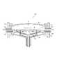
エピタキシャルウェーハの製造には、例えば枚葉式エピタキシャル成長装置が用いられる。ここで、一般的な枚葉式エピタキシャル成長装置について、図1を参照して説明する。図1に示すように、エピタキシャル成長装置100は、上部ドーム11、下部ドーム12及びドーム取付体13を含むチャンバ10を有し、該チャンバ10がエピタキシャル膜形成室を区画する。また、ドーム取付体13はサセプタを境界に上部ライナー17および下部ライナー18に区画される。チャンバ10には、その側面の対向する位置の上部ライナー17側に反応ガスGPの供給及び排出を行う反応ガス供給口15A及び反応ガス排出口16Aが設けられる。また、チャンバ10の側面の対向する位置の下部ライナー18側に、チャンバ内下部ドーム12の部分を水素雰囲気に保つための雰囲気ガスGAの供給及び排出を行う雰囲気ガス供給口15B及び雰囲気ガス排出口16Bが設けられる。For manufacturing an epitaxial wafer, for example, a single wafer epitaxial growth apparatus is used. Here, a general single wafer epitaxial growth apparatus will be described with reference to FIG. As shown in FIG. 1, the
また、チャンバ10内には、シリコンウェーハWが載置されるサセプタ20が配置される。サセプタ20は、下方からサセプタサポートシャフト30により支持される。サセプタサポートシャフト30は、アームの先端の3つの支持ピン(図示せず)でサセプタ20の下面外周部を勘合支持する。さらに、サセプタ20には3つの貫通孔(うち、1つは図示せず)が形成され、サセプタサポートシャフト30のアームにも貫通孔が1つずつ形成されている。これらアームの貫通孔及びサセプタの貫通孔には、リフトピン40A,40B,40C(ただし、リフトピン40Bは配置の都合により、図1の模式断面図では図示されない)が挿通される。また、リフトピン40の下端部は昇降シャフト50に支持される。チャンバ10内に搬入された半導体ウェーハWの支持、この半導体ウェーハWのサセプタ20上への載置、及び、気相成長後のエピタキシャルウェーハのチャンバ20外への搬出の際には、昇降シャフト50が昇降することで、リフトピン40がアームの貫通孔及びサセプタの貫通孔と摺動しながら昇降し、その上端部で半導体ウェーハWの昇降を行う。この枚葉式エピタキシャル成長装置エピタキシャル膜を成膜するときには、サセプタ20を回転させつつ、サセプタ20に載置された半導体ウェーハWの上面に反応ガスGPを接触させる。なお、反応ガスとは、キャリアガスにソースガスを混合させたガスを意味する。エピタキシャル層としてシリコンエピタキシャル層を形成する場合には、ソースガスはトリクロロシランガスなどのシリコンソースガスを用いる。A
ここで、サセプタ20の側面は、一般的に3mm程度の間隙を介して、プリヒートリング60により覆われる。プリヒートリング60は予熱リングまたは予加熱リングとも呼ばれ、反応ガスGPがエピタキシャル膜形成室に流入し、反応ガスGPが半導体ウェーハWと接触する前に、プリヒートリング60は反応ガスGPを予熱する。また、プリヒートリング60はサセプタ20の予熱も行う。こうすることで、成膜前および成膜中の半導体ウェーハWの熱均一性を高めて、エピタキシャル膜の均一性を高めることができる。Here, the side surface of the
なお、これまで、プリヒートリングを上面視した場合に、サセプタの中心点を対称とするリング状の形状とされてきた。エピタキシャル層を成膜させる際には上述のとおり、サセプタを回転させるため、サセプタとプリヒートリングとの接触を回避することがその理由の一つと言える。また、成膜前および成膜中の半導体の熱均一性を高めるためにも、プリヒートリングは半導体ウェーハあるいはサセプタの中心に対して対称構造であることが好ましいと考えられてきたためである。 Heretofore, when the preheat ring is viewed from above, it has been shaped like a ring with the center point of the susceptor symmetrical. As described above, when the epitaxial layer is formed, since the susceptor is rotated, it can be said that one of the reasons is to avoid contact between the susceptor and the preheat ring. In addition, it is considered that the preheat ring preferably has a symmetrical structure with respect to the center of the semiconductor wafer or the susceptor in order to improve the thermal uniformity of the semiconductor before and during the film formation.
特許文献1には、サセプタの周囲を囲み、反応ガスがガス供給口およびガス排出口間を移動する際に反応ガスを加熱するように作動する予加熱リング(プリヒートリング)を備えるエピタキシャル成長装置が記載されている。
ところで、枚葉式エピタキシャル成長装置により成膜した後のエピタキシャル層の厚み分布を測定すると、厚み分布にばらつきが見られる。近年、半導体デバイスの微細化が益々進むため、エピタキシャル層の厚み均一性を改善することのできる技術が求められる。 By the way, when the thickness distribution of the epitaxial layer after film formation is measured by the single-wafer epitaxial growth apparatus, the thickness distribution varies. In recent years, as semiconductor devices are increasingly miniaturized, a technique capable of improving the thickness uniformity of the epitaxial layer is required.
そこで本発明は、エピタキシャル層の厚み均一性を改善することのできるエピタキシャル成長装置を提供することを目的とする。 Therefore, an object of the present invention is to provide an epitaxial growth apparatus that can improve the thickness uniformity of an epitaxial layer.
本発明者は、この厚み分布のばらつきが生ずる原因について鋭意検討した。精度良くサセプタおよび半導体ウェーハの位置調整を行っても、サセプタおよび半導体ウェーハのそれぞれの中心は枚葉式エピタキシャル成長装置の中心軸に対してμmオーダーではずれが生じてしまう。したがって、プリヒートリングと、サセプタとの間隙の長さはサセプタ回転中に変動することとなり、反応ガスの流れに偏りが生じてしまうと考えられる。本発明者はこうした反応ガスの流れの偏りが、エピタキシャル層の厚み分布のばらつきの原因ではないかと考えた。そして、反応ガス供給口15A側での、プリヒートリングとサセプタとの間の間隙において、雰囲気ガスGAの吹き上がり変動が生じると、反応ガスGPが半導体ウェーハWの上面に不均一に接触することとなり、この場合に特にエピタキシャル層の厚み均一性が崩れやすいことを見出した。The inventor has intensively studied the cause of the variation in the thickness distribution. Even if the positions of the susceptor and the semiconductor wafer are adjusted with high accuracy, the centers of the susceptor and the semiconductor wafer are displaced in the order of μm with respect to the central axis of the single wafer epitaxial growth apparatus. Therefore, it is considered that the length of the gap between the preheat ring and the susceptor fluctuates during the susceptor rotation, and the reaction gas flow is biased. The present inventor thought that such a deviation in the flow of the reaction gas may be a cause of variations in the thickness distribution of the epitaxial layer. Then, in the reaction
ここで、図2を用いて、反応ガス排出口16Aおよび雰囲気ガス排出口16B側での、反応ガスGPおよび雰囲気ガスGAのガス流の流れを模式的に説明する。反応ガスGPは主として反応ガス排出口16A側に流れるが、サセプタ20とプリヒートリング60との間の間隙を介して、その一部が雰囲気ガス排出口16B側に沈み込む。反対に、雰囲気ガスGAは主として雰囲気ガス排出口16B側に流れるが、サセプタ20とプリヒートリング60との間の間隙を介して、その一部が反応ガス排出口16A側に吹き上がる。一般的にこの現象はチャンバ10の上部ドーム部分と下部ドーム部分の圧力差により生じる。Here, with reference to FIG. 2, in the
上述した反応ガス供給口15A側での雰囲気ガスGAの吹き上がりを抑制するためには、反応ガス排出口16A側での、プリヒートリング60とサセプタ20との間の間隙における、雰囲気ガスGAの吹き上がりを意図的に強くすればよいと本発明者は考えた。こうすることで、相対的に供給口15A側での雰囲気ガスGAの吹き上がり変動が抑制されるためである。そして、排出口16A側での雰囲気ガスGAの吹き上がりを強くするためには、例えばプリヒートリング60とサセプタ20との間の間隙の長さwを、供給口側での間隙の長さよりも大きくすればよいと本発明者は考えた。In order to suppress racing of the atmospheric gas GA in the above-mentioned reaction
本発明者はさらに鋭意検討した。排出口16A側で雰囲気ガスGAの吹き上がりを生じさせるためには、反応ガスGPの供給側におけるサセプタ20とプリヒートリング60との間隙幅よりも、広い間隙幅をサセプタ20とプリヒートリング60との間の少なくとも一部に設けることで、供給口15A側での吹き上がりを抑制できる。そして、こうしたエピタキシャル成長装置を用いれば上記課題を解決できることを本発明者は見出し、本発明を完成するに到った。The inventor has further studied diligently. To generate racing of the atmospheric gas GA at the
即ち、本発明の要旨構成は以下の通りである。
(1)半導体ウェーハの表面上にエピタキシャル膜を気相成長させるエピタキシャル成長装置であって、
チャンバと、
前記チャンバの内部で前記半導体ウェーハを載置するサセプタと、
前記サセプタの側面を間隙を介して覆うプリヒートリングと、
前記エピタキシャル層を気相成長させるための反応ガスを前記半導体ウェーハの上面に供給する反応ガス供給口と、を有し、
前記反応ガス供給口側における前記サセプタと前記プリヒートリングとの間隙幅よりも、広い間隙幅が前記サセプタと前記プリヒートリングとの間の少なくとも一部に設けられることを特徴とするエピタキシャル成長装置。That is, the gist configuration of the present invention is as follows.
(1) An epitaxial growth apparatus for vapor-phase growing an epitaxial film on the surface of a semiconductor wafer,
A chamber;
A susceptor for placing the semiconductor wafer inside the chamber;
A preheat ring that covers the side surface of the susceptor via a gap;
A reaction gas supply port for supplying a reaction gas for vapor phase growth of the epitaxial layer to the upper surface of the semiconductor wafer;
An epitaxial growth apparatus, wherein a gap width wider than a gap width between the susceptor and the preheating ring on the reactive gas supply port side is provided at least at a part between the susceptor and the preheating ring.
(2)前記反応ガス供給口との反対側における前記サセプタと前記プリヒートリングとの間隙幅が、前記反応ガス供給口側における前記サセプタと前記プリヒートリングとの間隙幅よりも広い、前記(1)に記載のエピタキシャル成長装置。(2) The gap width between the susceptor and the preheating ring on the side opposite to the reaction gas supply port is wider than the gap width between the susceptor and the preheating ring on the reaction gas supply port side. The epitaxial growth apparatus described in 1.
(3)前記プリヒートリングの外径と内径との差が周方向に不均一である、前記(1)または(2)に記載のエピタキシャル成長装置。(3) The epitaxial growth apparatus according to (1) or (2), wherein a difference between an outer diameter and an inner diameter of the preheat ring is not uniform in the circumferential direction.
(4)前記プリヒートリングの外周縁および内周縁は、互いに直径の異なる円形であり、かつ、前記外周縁の中心点と前記内周縁の中心点とが異なる、前記(3)に記載のエピタキシャル成長装置。(4) The epitaxial growth apparatus according to (3), wherein an outer peripheral edge and an inner peripheral edge of the preheat ring are circular with different diameters, and a central point of the outer peripheral edge is different from a central point of the inner peripheral edge. .
(5)前記プリヒートリングの内周縁に切り欠き部が設けられる、前記(3)に記載のエピタキシャル成長装置。(5) The epitaxial growth apparatus according to (3), wherein a notch is provided in an inner periphery of the preheat ring.
(6)前記プリヒートリングの外周縁は円形であり、かつ、前記プリヒートリングの内周縁は楕円形である、前記(3)に記載のエピタキシャル成長装置。(6) The epitaxial growth apparatus according to (3), wherein an outer peripheral edge of the preheating ring is circular, and an inner peripheral edge of the preheating ring is elliptical.
(7)エピタキシャル成長装置内で半導体ウェーハを載置するサセプタの側面を、間隙を介して覆うプリヒートリングであって、
前記プリヒートリングの外径と内径との差が周方向に不均一であることを特徴とするプリヒートリング。(7) A preheating ring that covers a side surface of a susceptor on which a semiconductor wafer is placed in an epitaxial growth apparatus through a gap,
A preheating ring, wherein a difference between an outer diameter and an inner diameter of the preheating ring is not uniform in a circumferential direction.
(8)前記プリヒートリングの外周縁および内周縁は、互いに直径の異なる円形であり、かつ、前記外周縁の中心点と前記内周縁の中心点とが異なる、前記(7)に記載のプリヒートリング。(8) The preheat ring according to (7), wherein an outer peripheral edge and an inner peripheral edge of the preheat ring are circular with different diameters, and a central point of the outer peripheral edge is different from a central point of the inner peripheral edge. .
(9)前記プリヒートリングの内周縁に切り欠き部が設けられる、前記(7)に記載のプリヒートリング。(9) The preheating ring according to (7), wherein a notch is provided in an inner peripheral edge of the preheating ring.
(10)前記プリヒートリングの外周縁は円形であり、かつ、前記プリヒートリングの内周縁は楕円形である、前記(7)に記載のプリヒートリング。(10) The preheating ring according to (7), wherein an outer peripheral edge of the preheating ring is circular and an inner peripheral edge of the preheating ring is elliptical.
(11)前記(1)〜(6)に記載のエピタキシャル成長装置または前記(7)〜(10)に記載のプリヒートリングを備えたエピタキシャル成長装置に、雰囲気ガスと、キャリアガスとしての水素ガスを含む反応ガスとを供給して、半導体ウェーハにエピタキシャル層をエピタキシャル成長させることを特徴とするエピタキシャルウェーハの製造方法。(11) Reaction including an atmosphere gas and hydrogen gas as a carrier gas in the epitaxial growth apparatus according to (1) to (6) or the epitaxial growth apparatus including the preheat ring according to (7) to (10) A method for producing an epitaxial wafer, wherein an epitaxial layer is epitaxially grown on a semiconductor wafer by supplying a gas.
本発明によれば、エピタキシャル膜の厚み均一性を改善することのできるエピタキシャル成長装置を提供することができる。 ADVANTAGE OF THE INVENTION According to this invention, the epitaxial growth apparatus which can improve the thickness uniformity of an epitaxial film can be provided.
以下、図面を参照して、本発明のリフトピンについて詳しく説明する。なお、図中の各構成の縦横比は、説明の便宜上誇張して図示しており、実際とは異なる。 Hereinafter, the lift pin of the present invention will be described in detail with reference to the drawings. Note that the aspect ratio of each component in the drawing is exaggerated for convenience of explanation, and is different from the actual one.
(エピタキシャル成長装置)
本発明の一実施形態に従うエピタキシャル成長装置は、半導体ウェーハWの表面上にエピタキシャル膜を気相成長させる。ここで、エピタキシャル成長装置100は、チャンバ10と、チャンバ10の内部で半導体ウェーハを載置するサセプタ20と、サセプタ20の側面を間隙を介して覆うプリヒートリング60と、エピタキシャル層を気相成長させるための反応ガスGPを半導体ウェーハWの上面に供給する反応ガス供給口15Aと、を有する。そして、従来技術と異なり、図3に例示するように、本実施形態に従うエピタキシャル成長装置100において、反応ガス供給口15A側におけるサセプタ20とプリヒートリング60との間隙幅w1よりも、広い間隙幅w2がサセプタ20とプリヒートリング60との間の少なくとも一部に設けられる。以下、各構成の詳細を順次説明する。(Epitaxial growth equipment)
An epitaxial growth apparatus according to an embodiment of the present invention causes an epitaxial film to vapor-phase grow on the surface of a semiconductor wafer W. Here, the
<チャンバ>
チャンバ10は、上部ドーム11、下部ドーム12及びドーム取付体13を含み、このチャンバ10がエピタキシャル膜形成室を区画する。チャンバ10には、上部ライナー17側での側面の対向する位置に反応ガスGPの供給及び排出を行う反応ガス供給口15A及び反応ガス排出口16Aが設けられることが一般的である。また、チャンバ10には、下部ライナー18側での側面の交差する位置に雰囲気ガスGAの供給及び排出を行う雰囲気ガス供給口15B及び雰囲気ガス排出口16Bが設けられることが一般的である。図1では簡略化するため、同一断面に反応ガスGPおよび雰囲気ガスGAの供給口および排出口を図示しており、図1のように反応ガスGPと雰囲気ガスGAとが並行するように供給口が設けられることもある。<Chamber>
The
<サセプタ>
サセプタ20は、チャンバ10の内部で半導体ウェーハWを載置する円盤状の部材である。サセプタ20は、一般的に周方向に120°等間隔で、表裏面を鉛直方向に貫通する3つの貫通孔を有する。これら貫通孔には、リフトピン40A,40B,40Cがそれぞれ挿通される。サセプタ20は、厚みが概ね2〜8mm程度であり、カーボングラファイト(黒鉛)を母材とし、その表面を炭化ケイ素(SiC:ビッカース硬度2,346kgf/mm2)でコーティングしたものを使用することができる。サセプタ20の表面には、半導体ウェーハWを収容し載置するザグリ部(図示せず)が形成されている。<Susceptor>
The
<プリヒートリング>
プリヒートリング60は、サセプタ20の側面を間隙を介して覆う。図示しないハロゲンランプから照射された光により加熱され、反応ガスGPがエピタキシャル膜形成室に流入し、反応ガスGPが半導体ウェーハWと接触する前に、プリヒートリング60は反応ガスGPを予熱する。プリヒートリング60はまた、サセプタ20の予熱も行う。このようにして、プリヒートリング60は成膜前および成膜中のサセプタ20および半導体ウェーハの熱均一性を高める。<Preheat ring>
The
プリヒートリング60は、サセプタ20と同様に、カーボングラファイト(黒鉛)を母材とし、その表面を炭化ケイ素(SiC:ビッカース硬度2,346kgf/mm2)でコーティングしたものを使用することができる。プリヒートリング60の厚みは、サセプタ20と同程度、もしくは厚くすることができ、例えば2mm〜6mmとすることができる。また、プリヒートリング60は水平に設置することが好ましいが、水平に対して±1度程度の傾斜は許容される。Similar to the
本明細書におけるサセプタ20とプリヒートリング60との間隙幅について、図3を参照して説明する。まず、プリヒートリング60が反応ガス供給口側に最も近い位置を基点Aとして、プリヒートリング60の外周縁の中心P1から時計回りにθ度回転させた位置でのサセプタ20とプリヒートリング60と間隙幅をwθと称することとする。図3に示すように、基点Aから、反応ガスのガス流れ方向に沿って上流側の間隙幅(w0°)を特にw1と称し、下流側の間隙幅(w180°)を特にw2と称することとする。図3の例では、反応ガス供給口側と対向する位置、すなわち反応ガスのガス流れ方向に沿って下流側の間隙幅w2が、最も広い間隙幅となり、上流側の間隙幅w1が最も狭い間隙幅となる。なお、プリヒートリング60の形状や、反応ガス供給口の設置領域にも依存するが、通常、外周縁の中心P1を中心として、プリヒートリング60と反応ガス供給口15Aとの最短距離となる位置Aを±45度回転させた領域を、本明細書におけるプリヒートリング60の反応ガス供給口側と言うこととする。なお、反応ガスGPは、図中の矢印の上流側から下流側へと流れ始め、サセプタ20が回転する際の遠心力の影響も受けるが、主として図中の矢印に沿って流れる。The gap width between the susceptor 20 and the
また、上述した間隙幅と同様に、図3に示すように、プリヒートリング60の外周縁の中心P1から時計回りにθ度回転させた位置でのプリヒートリング60の外径と内径との差をDθと称することとする。さらに、反応ガスのガス流れ方向に沿って上流側におけるプリヒートリング60の外径と内径との差(D0°)を特にD1と称し、下流側での外径と内径との差(D180°)をD2と称することとする。Similarly to the gap width as described above, as shown in FIG. 3, the difference between the outer diameter and the inner diameter of the
本実施形態では、プリヒートリング60の反応ガス供給口側を除く領域において、反応ガス供給口15A側におけるサセプタ20とプリヒートリング60との間隙幅よりも、広い間隙幅をサセプタ20とプリヒートリング60との間の少なくとも一部に設けることとする。この技術的意義を以下に説明する。 In the present embodiment, in the region excluding the reaction gas supply port side of the preheating
反応ガス供給口15A側で反応ガスGPが半導体ウェーハWの上面に不均一に接触することを抑制するためには、反応ガス供給口15A側での雰囲気ガスGAの吹き上がりを抑制すればよい。こうするためには、図2を用いて既述のとおり、例えば反応ガス排出口16A側での、プリヒートリング60とサセプタ20との間の間隙における、雰囲気ガスGAの吹き上がりを意図的に強くすればよい。また、反応ガス排出口16A側に限られず、反応ガス供給口15A側以外のところで、こうした雰囲気ガスGAの吹き上がりを意図的に強くする箇所を設けることでも、反応ガス供給口15A側での雰囲気ガスGAの吹き上がりを抑制することができる。To the reaction gas GP reaction
そこで、反応ガス供給口15A側におけるサセプタ20とプリヒートリング60との間隙幅よりも、広い間隙幅をサセプタ20とプリヒートリング60との間の少なくとも一部に設けられれば、反応ガス供給口15A側における雰囲気ガスGAの吹き上がりを低減し、反応ガスGPが半導体ウェーハWの上面に不均一に接触することを抑制することができる。そして、この結果、本実施形態に従うエピタキシャル成長装置100を用いて成膜したエピタキシャル層の厚み均一性を改善することができる。Therefore, if a gap width wider than the gap width between the susceptor 20 and the
この目的のため、反応ガス供給口側との反対側(すなわち反応ガス排出口側)におけるサセプタ20とプリヒートリング60との間隙幅が、反応ガス供給口側におけるサセプタと前記プリヒートリングとの間隙幅よりも広いことが好ましい。特に、反応ガス供給口側におけるサセプタ20とプリヒートリングとの間隙幅が最も狭いことが好ましく、また、反応ガス供給口側におけるサセプタとプリヒートリングとの間隙幅が、反応ガス供給口側との対向側に向かうにつれて漸減することも好ましい。さらに、プリヒートリング60の外径と内径との差が周方向に不均一であることも好ましい。 For this purpose, the gap width between the susceptor 20 and the preheating
上述した間隙幅を具現化することのできる具体例を、図3および図4を用いて説明する。ただし、本実施形態に適用可能なプリヒートリング60の形状はこれらに何ら限定されない。 A specific example capable of realizing the above-described gap width will be described with reference to FIGS. 3 and 4. However, the shape of the
図3に示すように、プリヒートリング60の外周縁および内周縁は、互いに直径の異なる円形であり、かつ、外周縁の中心点P1と内周縁の中心点P2の中心点とが異なることが好ましい。プリヒートリング60の外周縁および内周縁が互いに偏心しているということもできる。この場合、プリヒートリング60の外径と内径との差が周方向に一定でなくなり(すなわち、不均一)、間隙幅w1よりも、広い間隙幅がサセプタ20とプリヒートリング60との間に設けられることとなる。As shown in FIG. 3, the outer peripheral edge and the inner peripheral edge of the
この場合、プリヒートリング60の外周半径R1は220〜224mm程度とすることができ、また、内周半径R2は187〜191mm程度とすることができる。さらに、外周縁の中心点P1と内周縁の中心点P2との間の距離を1〜3mm程度とすることができる。図3の例では、サセプタ20とプリヒートリング60との間の最大の間隙幅はw2であり、最小の間隙幅はw1である。サセプタ20が周方向に回転しながらエピタキシャル成長する際のサセプタ20とプリヒートリング60との接触するによる発塵を防止するため、最小の間隙幅w1を1mm以上とすることが好ましく、一方、前述した反応ガス供給口側での雰囲気ガスGAの吹き上がりを抑制するため、最大の間隙幅w2を3mm以上とすることが好ましい。In this case, the outer peripheral radiusR 1 of the
また、図4(A)に示すように、プリヒートリング60の内周縁に切り欠き部が設けられることも好ましい。図4(A)の例では、プリヒートリング60の外周縁および内周縁は共通の中心点Pを有しているが、切り欠き部が設けられているため、反応ガス供給口側の間隙幅w1よりも、反応ガス供給口側と対向する位置での間隙幅w2の方が大きい。例えば、切り欠き部側での間隙幅w2を3mm〜10mm程度とし、反応ガス供給口側での間隙幅w1を1mm〜3mm程度とすることができる。また、切り欠き部側での外径と内径との差D2を29mm〜33mm程度とし、反応ガス供給口側での外径と内径との差D1を33mm〜34mm程度とすることができる。この例の場合、切り欠き部で雰囲気ガスの吹き上がりが強くなるため、結果的に反応ガス供給口側での雰囲気ガスの吹き上がりを抑制することができる。Further, as shown in FIG. 4A, it is also preferable that a notch portion is provided on the inner peripheral edge of the
さらに、図4(B)に示すように、プリヒートリング60の外周縁は円形であり、かつ、プリヒートリング60の内周縁は楕円形であることも好ましい。図4(A)の例では、プリヒートリング60の外周縁および内周縁は共通の中心点Pを有しているが、内周縁の楕円形の短軸は反応ガスのガス流れに沿い、内周縁の楕円形の長軸は反応ガスのガス流れに垂直な方向に沿っている。この場合、反応ガスのガス流れに沿う方向での間隙幅w1,w2を1mm〜3mm程度とし、反応ガスのガス流れに垂直な方向での間隙幅w3(W90°)を3mm〜10mm程度とすることができる。さらに、反応ガスのガス流れに沿う方向での外径と内径との差D1,D2を33mm〜34mm程度とし、反応ガスのガス流れに垂直な方向での外径と内径との差D3(D90°)を29mm〜33mm程度とすることができる。この例の場合、プリヒートリング60の長軸側で雰囲気ガスの吹き上がりが強くなるため、結果的に反応ガス供給口側での雰囲気ガスの吹き上がりを抑制することができる。Further, as shown in FIG. 4B, it is also preferable that the outer peripheral edge of the
また、図4(C)に示すように、プリヒートリング60の外周縁を円形とする一方で、内周縁を非円形とすることも好ましい。図4(C)の例では、プリヒートリング60の外周縁および内周縁は共通の中心点Pを有しているが、内周縁のうち、図の左半分は円であり、図の右半分は楕円の一部である。そして、反応ガス供給口側の間隙幅w1よりも、反応ガス供給口側と対向する位置での間隙幅w2の方が大きくなっている。この例の場合でも、内周縁の楕円側で雰囲気ガスの吹き上がりが強くなるため、結果的に反応ガス供給口側での雰囲気ガスの吹き上がりを抑制することができる。図4(C)の場合、間隙幅w2を3mm〜15mm程度とし、間隙幅w1を1mm〜3mm程度とすることができる。また、外径と内径との差D2を26mm〜33mm程度とし、外径と内径との差D1を33mm〜34mm程度とすることができる。また、図4(C)では、図中の内周縁の右半分のみを楕円形の輪郭としたが、長円形の輪郭としてもよいし、放物線形状の輪郭としても構わないし、反応ガス供給口側以外であればどこに非円形を設けても構わない。Moreover, as shown in FIG.4 (C), while making the outer periphery of the
以上、プリヒートリング60の種々の好適態様を説明したが、前述のとおり、反応ガス供給口側におけるサセプタ20とプリヒートリング60との間隙幅よりも、広い間隙幅をサセプタ20とプリヒートリング60との間の少なくとも一部に設ければ、反応ガス供給口側における雰囲気ガスの吹き上がりを抑制することができ、結果、エピタキシャル層の膜厚均一性を改善することができる。 As described above, various preferred embodiments of the preheating
本実施形態に従うエピタキシャル成長装置では、半導体ウェーハWとしてシリコンウェーハを用いることが好ましく、シリコンウェーハ上に成膜するエピタキシャル層はシリコンエピタキシャル層であることが好ましい。ただし、本実施形態に従うエピタキシャル成長装置は化合物半導体ウェーハなどにも適用可能であり、ヘテロエピタキシャル成長にも適用可能である。 In the epitaxial growth apparatus according to this embodiment, a silicon wafer is preferably used as the semiconductor wafer W, and the epitaxial layer formed on the silicon wafer is preferably a silicon epitaxial layer. However, the epitaxial growth apparatus according to this embodiment can be applied to a compound semiconductor wafer or the like, and can also be applied to heteroepitaxial growth.
さらに、本実施形態に従うエピタキシャル成長装置は、以下のサセプタサポートシャフト、リフトピン、昇降シャフト、加熱ランプおよびエピタキシャル成長装置に用いられる一般的な構成を有することができる。たたし、本実施形態はこれらの具体的な態様に何ら限定されない。 Furthermore, the epitaxial growth apparatus according to the present embodiment can have a general configuration used for the following susceptor support shaft, lift pin, lifting shaft, heating lamp, and epitaxial growth apparatus. However, the present embodiment is not limited to these specific aspects.
<サセプタサポートシャフト>
サセプタサポートシャフト30は、チャンバ10内でサセプタ20を下方から支持するものであり、その支柱は、サセプタ20の中心とほぼ同軸上に配置される。<Susceptor support shaft>
The
<リフトピン>
リフトピン40A,40B,40Cは、サセプタ20の貫通孔にそれぞれ挿通される。リフトピン40A,40B,40Cは、昇降シャフト50によって、上下方向に昇降されることにより、リフトピンの上端部で半導体ウェーハW(半径50%以上の裏面部領域)を支持しながら半導体ウェーハWをサセプタ20上に着脱させることができる。この動作についても詳細は後述する。リフトピン40A,40B,40Cの材料には、サセプタ20と同様に、カーボングラファイトおよび/または炭化ケイ素が用いられることが一般的である。<Lift pin>
The lift pins 40A, 40B, and 40C are inserted through the through holes of the
<昇降シャフト>
昇降シャフト50は、サセプタサポートシャフト30の主柱を収容する中空を区画し、支柱の先端部でリフトピンの下端部をそれぞれ支持する。昇降シャフト50は石英で構成されることが好ましい。昇降シャフトが、サセプタサポートシャフト30の主柱に沿って上下動することにより、リフトピン40A,40B,40Cを昇降させることができる。<Elevating shaft>
The elevating
<加熱ランプ>
加熱ランプは、チャンバ10の上側領域および下側領域に配置され、一般に、昇降温速度が速く、温度制御性に優れた、ハロゲンランプや赤外ランプが用いられる。<Heating lamp>
The heating lamp is disposed in the upper region and the lower region of the
(プリヒートリング)
また、本発明の一実施形態に従うプリヒートリングは、エピタキシャル成長装置内で半導体ウェーハを載置するサセプタの側面を、間隙を介して覆うプリヒートリングである。そして、プリヒートリングの外径と内径との差が周方向に不均一である。こうしたプリヒートリングをエピタキシャル成長装置に用いれば、前述したとおりエピタキシャルの反応ガス供給口側における雰囲気ガスの吹き上がりを抑制でき、その結果、エピタキシャル層の膜厚均一性を改善することができる。このようなプリヒートリングの好適態様を、既述の図3,4を用いて説明するが、エピタキシャル成長装置の実施形態と重複する説明は省略する。(Preheat ring)
The preheat ring according to the embodiment of the present invention is a preheat ring that covers the side surface of the susceptor on which the semiconductor wafer is placed in the epitaxial growth apparatus via a gap. The difference between the outer diameter and the inner diameter of the preheat ring is not uniform in the circumferential direction. If such a preheat ring is used in an epitaxial growth apparatus, as described above, blowing up of atmospheric gas on the epitaxial reaction gas supply port side can be suppressed, and as a result, film thickness uniformity of the epitaxial layer can be improved. A preferred embodiment of such preheating will be described with reference to FIGS. 3 and 4 described above, but the description overlapping with the embodiment of the epitaxial growth apparatus will be omitted.
また、図3に示すように、プリヒートリング60の外周および内周は、互いに直径の異なる円形であり、かつ、外周の中心点P1と内周の中心点P2とが異なることが好ましい。さらに、図4(A)に示すように、プリヒートリング60の内周に切り欠き部が設けられることも好ましい。さらにまた、プリヒートリング60の外周は円形であり、かつ、プリヒートリング60の内周は楕円形であることも好ましい。Further, as shown in FIG. 3, the outer and inner periphery of the
また、本発明の一実施形態に従うエピタキシャルウェーハの製造方法は、前述のエピタキシャル成長装置またはプリヒートリングを備えたエピタキシャル成長装置に、雰囲気ガスと、キャリアガスとしての水素ガスを含む反応ガスとを供給して、半導体ウェーハにエピタキシャル層をエピタキシャル成長させる。こうすることで、前述したとおりエピタキシャルの反応ガス供給口側における雰囲気ガスの吹き上がりを抑制できる。 The epitaxial wafer manufacturing method according to one embodiment of the present invention supplies an atmospheric gas and a reaction gas containing hydrogen gas as a carrier gas to the above-described epitaxial growth apparatus or an epitaxial growth apparatus provided with a preheat ring. An epitaxial layer is epitaxially grown on a semiconductor wafer. By doing so, it is possible to suppress the blowing up of the atmospheric gas on the epitaxial reaction gas supply port side as described above.
なお、キャリアガスとしての水素ガスを含む反応ガスを供給する際の流量は5〜100SLMとすることができ、雰囲気ガスを供給をする際の流量は1〜50SLMとすることができる。また、キャリアガスとしては水素ガスを用いることが好ましく、シリコンのソースガスとしてはジクロロシラン、トリクロロシランなどを用いることが好ましい。さらに、雰囲気ガスとしては水素ガスを用いることが好ましい。また、半導体ウェーハWとしてシリコンウェーハを用いることが好ましく、シリコンウェーハ上に成膜するエピタキシャル層はシリコンエピタキシャル層であることが好ましい。 In addition, the flow rate at the time of supplying the reactive gas containing hydrogen gas as carrier gas can be 5-100 SLM, and the flow rate at the time of supplying atmospheric gas can be 1-50 SLM. Further, hydrogen gas is preferably used as the carrier gas, and dichlorosilane, trichlorosilane, or the like is preferably used as the silicon source gas. Furthermore, it is preferable to use hydrogen gas as the atmospheric gas. Moreover, it is preferable to use a silicon wafer as the semiconductor wafer W, and the epitaxial layer formed on the silicon wafer is preferably a silicon epitaxial layer.
次に、本発明の効果をさらに明確にするため、以下の実施例を挙げるが、本発明は以下の実施例に何ら制限されるものではない。 Next, in order to further clarify the effects of the present invention, the following examples are given, but the present invention is not limited to the following examples.
[実験例1]
(発明例1)
図3に示すプリヒートリング60をエピタキシャル成長装置に設置した。図3と同様に、プリヒートリング60の外径と内径との差が最小となる位置を反応ガス供給口側とし、プリヒートリング60の外径と内径との差が最大となる位置を反応ガス排出口側とした。図3に示す中心点P1とP2との間の距離は1.5mmであり、また、サセプタ20とプリヒートリング60との間の間隙幅w1は2mmであり、間隙幅w2は5mmである。[Experimental Example 1]
(Invention Example 1)
The
シリコンエピタキシャルウェーハの基板としては、ボロンドープされた直径300mmのシリコンウェーハWを用いた。このシリコンウェーハW上に、発明例1によるエピタキシャル成長装置を用いてエピタキシャルウェーハを製造した。エピタキシャルウェーハの製造にあたり、まず、原料ソースガスであるトリクロロシランガスを温度1130℃にて供給し、サセプタ20の表面に対してシリコンコートを施した。次いで、シリコンウェーハWをエピタキシャル膜形成室内に導入し、リフトピンを用いてサセプタ20上に載置した。続いて、1130℃にて、水素ガスを供給し、水素ベークを行った後、1130℃にて、シリコンのエピタキシャル膜を4μm成長させてエピタキシャルシリコンウェーハを得た。ここで、原料ソースガスとしてはトリクロロシランガスを用い、また、ドーパントガスとしてジボランガス、キャリアガスとして水素ガスを用いた。また、反応ガスGPの合計流量(ソースガスおよびキャリアガスの合計流量)は70SLMとし、雰囲気ガスGAの流量は25SLMとした。 As a substrate of the silicon epitaxial wafer, a boron-doped silicon wafer W having a diameter of 300 mm was used. An epitaxial wafer was manufactured on the silicon wafer W using the epitaxial growth apparatus according to Invention Example 1. In manufacturing the epitaxial wafer, first, trichlorosilane gas as a source gas was supplied at a temperature of 1130 ° C., and the surface of the
(従来例)
発明例1におけるプリヒートリング60に替えて、従来技術に係る、中心点を対称とするリング状のプリヒートリングを用いた以外は、発明例1と同様にしてエピタキシャル層を成膜した。なお、従来例におけるプリヒートリングとサセプタとの間の間隙の長さは3.5mm程度で周方向に均一である。(Conventional example)
In place of the preheating
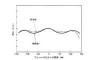
<評価:エピタキシャル層の膜厚測定>
FT−IR方式の膜厚測定器(ナノメトリクス社製:QS−3300EG)を用いて、発明例1および従来例により作製したエピタキシャルウェーハのエピタキシャル膜の膜厚分布をそれぞれ測定した。結果を図5に示す。ただし、図5のグラフの縦軸は相対値により示す。図5から、エピタキシャルウェーハの100mmより外側の厚み分布ばらつきは従来例に比べて約58%改善したことが確認できる。なお、ここで言う「ばらつき」とは、上記膜厚測定器によるウェーハ外周部(ウェーハ中心から半径100mm以内を除外)における測定値のばらつき度合いを意味し、{(最大測定値−最小測定値)/(最大測定値+最小測定値)}×100%により定義する。以下の実験例2,3においても同様である。<Evaluation: Measurement of film thickness of epitaxial layer>
The film thickness distribution of the epitaxial film of the epitaxial wafer produced by the invention example 1 and the prior art example was measured using the FT-IR type film thickness measuring device (manufactured by Nanometrics: QS-3300EG). The results are shown in FIG. However, the vertical axis of the graph of FIG. From FIG. 5, it can be confirmed that the thickness distribution variation of the epitaxial wafer outside 100 mm is improved by about 58% compared to the conventional example. The term “variation” as used herein means the degree of variation in the measured value at the wafer outer periphery (excluding the radius within 100 mm from the wafer center) by the film thickness measuring instrument, and {(maximum measured value−minimum measured value) / (Maximum measurement value + minimum measurement value)} × 100%. The same applies to Experimental Examples 2 and 3 below.
[実験例2]
発明例1におけるプリヒートリングの外周半径R1および内周半径R2を維持しつつ、外周中心P1と内周中心P2との距離を変えた以外は、発明例1と同様にしてシリコンエピタキシャルシャルウェーハを作製した。図6に、外周中心P1と内周中心P2との距離と、厚み分布ばらつきとの関係性を示す。なお、外周中心P1と内周中心P2との距離が3mm以上となる、w1がほとんど0となり接触するため、正常にエピタキシャル成長できなかった。[Experiment 2]
While maintaining the outer peripheral radius R1 and inner radius R2 of the preheat ring in invention Example 1, except for changing the distance between the inner peripheral center P2 and the outer peripheral center P1, the silicon epitaxial in the same manner as Inventive Example 1 A partial wafer was produced. Figure 6 shows the distance between the inner circumferential center P2 and the outer peripheral center P1, the relationship between the thickness distribution variation. The distance between the inner circumferential center P2 is equal to or greater than 3mm and the outer peripheral center P1, since w1 is almost zero contact, it could not be successfully epitaxial growth.
図6から、発明例1では、w1が1mm以下とならない程度において、w2を広くするほど、従来例に比べて外周方向での膜厚分布のばらつきを改善できることが確認できる。特に、外周中心P1と内周中心P2との距離が1mm以上であると、ばらつきを0.6%以下とできたことが確認できる。本発明条件に従うエピタキシャル装置を用いることで、エピタキシャル装置内での反応ガス供給口側での雰囲気ガスの吹き上がりが抑制できたため、膜厚均一性を改善できたのだと推定される。From FIG. 6, it can be confirmed that in Invention Example 1, the variation in film thickness distribution in the outer peripheral direction can be improved as w2 is widened to the extent that w1 does not become1 mm or less. In particular, the distance between the inner circumferential center P2 and the outer peripheral center P1 is at 1mm or more, the variation can be seen that was 0.6% or less. By using the epitaxial apparatus according to the conditions of the present invention, it is presumed that the film thickness uniformity could be improved because the blowing up of the atmospheric gas on the reaction gas supply port side in the epitaxial apparatus could be suppressed.
[実験例3]
図7(A)に示すように、発明例1におけるプリヒートリングの外周半径R1および内周半径R2を維持し、外周中心P1に対して反応ガス供給口側に最も近い点Aと、プリヒートリング60とサセプタ20との間隙幅が最小となる位置Bとがなす角度φを回転させた以外は、発明例1と同様にしてシリコンエピタキシャルウェーハを作製した。(発明例1では、角度φは0°であった。)なお、図7では説明の便宜上、図3におけるw1(最小間隙幅),w2(最大間隙幅)等の符号を位置関係を明確に対比するためそのまま用いている。したがって、反応ガス供給口側に最も近い点Aにおけるプリヒートリング60と、サセプタ20との間隙幅wφは、w1<wφ<w2となる。角度φに関し、図7(A)のように基点Aから間隙幅が最小となる位置Bへ反時計回りに進む場合は角度φをマイナスの角度として扱い、反対に、基点Aから間隙幅が最小となる位置Bへ時計回りに進む場合は、角度φをプラスの角度として扱うものとする。なお、実験例2とは異なり、外周中心P1と内周中心P2との距離を1.5mmに維持している。[Experiment 3]
As shown in FIG. 7 (A), a point A that maintains the outer peripheral radius R1 and the inner peripheral radius R2 of the preheating ring in Invention Example 1 and is closest to the reaction gas supply port side with respect to the outer peripheral center P1 ; A silicon epitaxial wafer was fabricated in the same manner as in Invention Example 1, except that the angle φ formed by the position B at which the gap width between the
図7(B)に、角度φと、厚み分布ばらつきとの関係性を示す。中心点P1に対して、反応ガス供給口側である基点Aと、間隙幅が最小となる位置Bとがなす角度φがプラスマイナス45°のときに0.8%であったため、図7(B)より、角度φをプラスマイナス45°の範囲内とすれば、厚み分布ばらつきを抑制できることが確認された。特に、角度φを−40°から+15°とすることで、厚み分布ばらつきを0.6%以下とすることができ、高い効果が得られることが確認される。なお、図7(B)のグラフにおいて、φが0°のときを中心に対称とならないのは、サセプタが時計回りに回転していることがその原因の一つであると推定される。FIG. 7B shows the relationship between the angle φ and the thickness distribution variation. Since the angle φ formed by the base point A on the reactive gas supply port side and the position B at which the gap width is minimum with respect to the center point P1 was 0.8%, it was 0.8%. From (B), it was confirmed that variation in thickness distribution can be suppressed if the angle φ is in the range of plus or minus 45 °. In particular, by setting the angle φ to −40 ° to + 15 °, the thickness distribution variation can be reduced to 0.6% or less, and it is confirmed that a high effect can be obtained. In the graph of FIG. 7B, it is estimated that one of the causes is that the susceptor is rotating clockwise when φ is 0 °.
本発明によれば、エピタキシャル膜の厚み均一性を改善することのできるエピタキシャル成長装置を提供することができる。 ADVANTAGE OF THE INVENTION According to this invention, the epitaxial growth apparatus which can improve the thickness uniformity of an epitaxial film can be provided.
100 エピタキシャル成長装置
10 チャンバ
11 上部ドーム
12 下部ドーム
13 ドーム取付体
14 加熱ランプ
15A 反応ガス供給口
15B 雰囲気ガス供給口
16A 反応ガス排出口
16B 雰囲気ガス排出口
17 上部ライナー
18 下部ライナー
20 サセプタ
30 サセプタサポートシャフト
40A,40C リフトピン
50 昇降シャフト
60 プリヒートリング
W 半導体ウェーハDESCRIPTION OF
Claims (7)
Translated fromJapaneseチャンバと、
前記チャンバの内部で前記半導体ウェーハを載置するサセプタと、
前記サセプタの側面を間隙を介して覆うプリヒートリングと、
前記エピタキシャル層を気相成長させるための反応ガスを前記半導体ウェーハの上面に供給する反応ガス供給口と、を有し、
前記反応ガス供給口側における前記サセプタと前記プリヒートリングとの間隙幅よりも、広い間隙幅が前記サセプタと前記プリヒートリングとの間の少なくとも一部に設けられ、
前記プリヒートリングの外周縁および内周縁は、互いに直径の異なる円形であり、かつ
、前記外周縁の中心点と前記内周縁の中心点とが異なり、
さらに、前記外周縁の中心点に対して、前記反応ガス供給口側に最も近い点と、前記間隙幅が最小となる位置とがなす角度が、前記サセプタの回転方向を正として−40°以上0°以下(ただし、0°を除く)であることを特徴とするエピタキシャル成長装置。An epitaxial growth apparatus for vapor-phase growing an epitaxial film on the surface of a semiconductor wafer,
A chamber;
A susceptor for placing the semiconductor wafer inside the chamber;
A preheat ring that covers the side surface of the susceptor via a gap;
A reaction gas supply port for supplying a reaction gas for vapor phase growth of the epitaxial layer to the upper surface of the semiconductor wafer;
A gap width wider than the gap width between the susceptor and the preheat ring on the reactive gas supply port side is provided in at least a part between the susceptor and the preheat ring,
The outer periphery and the inner periphery of the preheat ring are circular with different diameters, and
, The central point of the outer peripheral edge and the central point of the inner peripheral edge are different,
Further, an angle formed by a point closest to the reactive gas supply port side with respect to the center point of the outer peripheral edge and a position where the gap width is minimum is −40 ° or more with the rotation direction of the susceptor being positive. 0 ° or less (excluding 0 °) der Rukoto epitaxial growth apparatus according to claim.
前記プリヒートリングの外径と内径との差が周方向に不均一であり、
前記プリヒートリングの外周縁および内周縁は、互いに直径の異なる円形であり、かつ、前記外周縁の中心点と前記内周縁の中心点とが異なり、
さらに、前記外周縁の中心点に対して、前記反応ガス供給口側に最も近い点と、前記間隙幅が最小となる位置とがなす角度が、前記サセプタの回転方向を正として−40°以上0°以下(ただし、0°を除く)であることを特徴とするプリヒートリング。A preheating ring that covers a side surface of a susceptor on which a semiconductor wafer is placed in an epitaxial growth apparatus through a gap,
WhereinRi heterogeneous der difference in the circumferential direction between the outer diameter and the inner diameter of the preheatring,
The outer peripheral edge and inner peripheral edge of the preheat ring is a different circular diameters from each other, and,Ri said outer peripheral edge center point and the center point of the inner peripheral edge Do differentof,
Further, an angle formed by a point closest to the reactive gas supply port side with respect to the center point of the outer peripheral edge and a position where the gap width is minimum is −40 ° or more with the rotation direction of the susceptor being positive. A preheating ringcharacterized by being 0 ° or less (excluding 0 °) .
Priority Applications (7)
| Application Number | Priority Date | Filing Date | Title |
|---|---|---|---|
| JP2017043202AJP6330941B1 (en) | 2017-03-07 | 2017-03-07 | Epitaxial growth apparatus, preheat ring, and epitaxial wafer manufacturing method using them |
| PCT/JP2018/007889WO2018163975A1 (en) | 2017-03-07 | 2018-03-01 | Epitaxial growth device and preheat ring, and epitaxial wafer manufacturing method using same |
| DE112018001223.9TDE112018001223B4 (en) | 2017-03-07 | 2018-03-01 | Epitaxial growth apparatus, preheat ring, and method of making epitaxial wafers using the same |
| CN201880016731.1ACN110494957B (en) | 2017-03-07 | 2018-03-01 | Epitaxial growth device, preheat ring, and method for manufacturing epitaxial wafer using these |
| US16/482,800US10975495B2 (en) | 2017-03-07 | 2018-03-01 | Epitaxial growth apparatus, preheat ring, and method of manufacturing epitaxial wafer using these |
| KR1020197022406AKR102243261B1 (en) | 2017-03-07 | 2018-03-01 | Epitaxial growth apparatus and preheat ring, and manufacturing method of epitaxial wafer using them |
| TW107107441ATWI664310B (en) | 2017-03-07 | 2018-03-06 | Epitaxial growth device, preheating ring, and manufacturing method of epitaxial wafer using the same |
Applications Claiming Priority (1)
| Application Number | Priority Date | Filing Date | Title |
|---|---|---|---|
| JP2017043202AJP6330941B1 (en) | 2017-03-07 | 2017-03-07 | Epitaxial growth apparatus, preheat ring, and epitaxial wafer manufacturing method using them |
Related Child Applications (1)
| Application Number | Title | Priority Date | Filing Date |
|---|---|---|---|
| JP2018083433ADivisionJP6521140B2 (en) | 2018-04-24 | 2018-04-24 | Epitaxial growth apparatus and preheat ring, and method of manufacturing epitaxial wafer using them |
Publications (2)
| Publication Number | Publication Date |
|---|---|
| JP6330941B1true JP6330941B1 (en) | 2018-05-30 |
| JP2018148098A JP2018148098A (en) | 2018-09-20 |
Family
ID=62236462
Family Applications (1)
| Application Number | Title | Priority Date | Filing Date |
|---|---|---|---|
| JP2017043202AActiveJP6330941B1 (en) | 2017-03-07 | 2017-03-07 | Epitaxial growth apparatus, preheat ring, and epitaxial wafer manufacturing method using them |
Country Status (7)
| Country | Link |
|---|---|
| US (1) | US10975495B2 (en) |
| JP (1) | JP6330941B1 (en) |
| KR (1) | KR102243261B1 (en) |
| CN (1) | CN110494957B (en) |
| DE (1) | DE112018001223B4 (en) |
| TW (1) | TWI664310B (en) |
| WO (1) | WO2018163975A1 (en) |
Cited By (3)
| Publication number | Priority date | Publication date | Assignee | Title |
|---|---|---|---|---|
| CN111288889A (en)* | 2020-01-17 | 2020-06-16 | 北京北方华创微电子装备有限公司 | Position detection device and position detection method of chamber process assembly |
| CN111599716A (en)* | 2020-05-06 | 2020-08-28 | 北京北方华创微电子装备有限公司 | Preheating ring for epitaxial growth equipment and epitaxial growth equipment |
| CN112768384A (en)* | 2021-01-26 | 2021-05-07 | 西安奕斯伟硅片技术有限公司 | Preheating ring and wafer epitaxial growth equipment |
Families Citing this family (14)
| Publication number | Priority date | Publication date | Assignee | Title |
|---|---|---|---|---|
| CN111304740A (en)* | 2018-12-11 | 2020-06-19 | 西安奕斯伟硅片技术有限公司 | Epitaxial growth device and manufacturing method thereof |
| JP7159986B2 (en)* | 2019-06-27 | 2022-10-25 | 株式会社Sumco | Epitaxial growth apparatus and epitaxial wafer manufacturing method |
| CN113327884B (en)* | 2020-02-29 | 2023-10-17 | 长鑫存储技术有限公司 | Wafer support, wafer processing device and wafer processing method |
| CN111477565B (en)* | 2020-03-26 | 2023-06-16 | 北京北方华创微电子装备有限公司 | Epitaxial equipment |
| JP7361005B2 (en)* | 2020-09-18 | 2023-10-13 | 株式会社Kokusai Electric | Substrate processing equipment, substrate holder, semiconductor device manufacturing method, and program |
| EP3978647A1 (en) | 2020-09-30 | 2022-04-06 | Siltronic AG | Method and device for depositing an epitaxial layer on a substrate wafer of semiconductor material |
| JP7549871B2 (en)* | 2020-10-12 | 2024-09-12 | エピクルー株式会社 | Vapor phase growth apparatus and epitaxial wafer manufacturing method |
| US12252806B2 (en) | 2020-12-31 | 2025-03-18 | Globalwafers Co., Ltd | Systems and methods for a preheat ring in a semiconductor wafer reactor |
| KR102582346B1 (en)* | 2021-03-30 | 2023-09-25 | 에스케이실트론 주식회사 | Method for growing epitaxial layer on wafer |
| EP4098782A1 (en) | 2021-06-01 | 2022-12-07 | Siltronic AG | Method for depositing an epitaxial layer on a substrate wafer made of semiconductor material in a deposition apparatus |
| CN113981531B (en)* | 2021-10-26 | 2022-10-04 | 江苏天芯微半导体设备有限公司 | Preheating ring and substrate processing equipment |
| CN115584553A (en)* | 2022-11-04 | 2023-01-10 | 西安奕斯伟材料科技有限公司 | Preheating ring and wafer epitaxial growth equipment |
| US20240247404A1 (en)* | 2023-01-25 | 2024-07-25 | Applied Materials, Inc. | Pre-heat rings and processing chambers including black quartz, and related methods |
| CN119465082B (en)* | 2024-11-08 | 2025-08-22 | 研微(江苏)半导体科技有限公司 | Semiconductor reaction chamber and method of using the same |
Family Cites Families (14)
| Publication number | Priority date | Publication date | Assignee | Title |
|---|---|---|---|---|
| DE69404397T2 (en) | 1993-07-13 | 1997-11-13 | Applied Materials Inc | Improved susceptor design |
| JP2003197532A (en)* | 2001-12-21 | 2003-07-11 | Sumitomo Mitsubishi Silicon Corp | Epitaxial growth method and epitaxial growth suscepter |
| JP3758579B2 (en) | 2002-01-23 | 2006-03-22 | 信越半導体株式会社 | Heat treatment apparatus and heat treatment method |
| JP4379585B2 (en)* | 2003-12-17 | 2009-12-09 | 信越半導体株式会社 | Vapor phase growth apparatus and epitaxial wafer manufacturing method |
| WO2005124845A1 (en)* | 2004-06-15 | 2005-12-29 | Hitachi Kokusai Electric Inc. | Substrate processing equipment and semiconductor device manufacturing method |
| JP5004513B2 (en)* | 2006-06-09 | 2012-08-22 | Sumco Techxiv株式会社 | Vapor growth apparatus and vapor growth method |
| JP5195176B2 (en)* | 2008-08-29 | 2013-05-08 | 東京エレクトロン株式会社 | Deposition equipment |
| US9890455B2 (en)* | 2010-10-29 | 2018-02-13 | Applied Materials, Inc. | Pre-heat ring designs to increase deposition uniformity and substrate throughput |
| JP5477314B2 (en)* | 2011-03-04 | 2014-04-23 | 信越半導体株式会社 | Susceptor and epitaxial wafer manufacturing method using the same |
| JP5602903B2 (en)* | 2013-03-14 | 2014-10-08 | アプライド マテリアルズ インコーポレイテッド | Epitaxial film formation method and epitaxial growth apparatus |
| US9814099B2 (en)* | 2013-08-02 | 2017-11-07 | Applied Materials, Inc. | Substrate support with surface feature for reduced reflection and manufacturing techniques for producing same |
| US10047457B2 (en) | 2013-09-16 | 2018-08-14 | Applied Materials, Inc. | EPI pre-heat ring |
| KR101539298B1 (en)* | 2013-11-25 | 2015-07-29 | 주식회사 엘지실트론 | Apparatus for Growing Epitaxial Wafer |
| JP6341083B2 (en)* | 2014-12-25 | 2018-06-13 | 株式会社Sumco | Epitaxial silicon wafer manufacturing method |
- 2017
- 2017-03-07JPJP2017043202Apatent/JP6330941B1/enactiveActive
- 2018
- 2018-03-01WOPCT/JP2018/007889patent/WO2018163975A1/ennot_activeCeased
- 2018-03-01DEDE112018001223.9Tpatent/DE112018001223B4/enactiveActive
- 2018-03-01USUS16/482,800patent/US10975495B2/enactiveActive
- 2018-03-01KRKR1020197022406Apatent/KR102243261B1/enactiveActive
- 2018-03-01CNCN201880016731.1Apatent/CN110494957B/enactiveActive
- 2018-03-06TWTW107107441Apatent/TWI664310B/enactive
Cited By (4)
| Publication number | Priority date | Publication date | Assignee | Title |
|---|---|---|---|---|
| CN111288889A (en)* | 2020-01-17 | 2020-06-16 | 北京北方华创微电子装备有限公司 | Position detection device and position detection method of chamber process assembly |
| CN111599716A (en)* | 2020-05-06 | 2020-08-28 | 北京北方华创微电子装备有限公司 | Preheating ring for epitaxial growth equipment and epitaxial growth equipment |
| CN112768384A (en)* | 2021-01-26 | 2021-05-07 | 西安奕斯伟硅片技术有限公司 | Preheating ring and wafer epitaxial growth equipment |
| CN112768384B (en)* | 2021-01-26 | 2024-02-27 | 西安奕斯伟材料科技股份有限公司 | Preheating ring and wafer epitaxial growth equipment |
Also Published As
| Publication number | Publication date |
|---|---|
| US20200354853A1 (en) | 2020-11-12 |
| CN110494957B (en) | 2023-05-02 |
| TW201842221A (en) | 2018-12-01 |
| KR102243261B1 (en) | 2021-04-21 |
| DE112018001223B4 (en) | 2021-11-25 |
| JP2018148098A (en) | 2018-09-20 |
| US10975495B2 (en) | 2021-04-13 |
| CN110494957A (en) | 2019-11-22 |
| DE112018001223T5 (en) | 2019-11-21 |
| TWI664310B (en) | 2019-07-01 |
| KR20190100365A (en) | 2019-08-28 |
| WO2018163975A1 (en) | 2018-09-13 |
Similar Documents
| Publication | Publication Date | Title |
|---|---|---|
| JP6330941B1 (en) | Epitaxial growth apparatus, preheat ring, and epitaxial wafer manufacturing method using them | |
| KR101139132B1 (en) | Susceptor for vapor growth apparatus | |
| JP6424726B2 (en) | Susceptor and epitaxial growth apparatus | |
| JP4592849B2 (en) | Semiconductor manufacturing equipment | |
| EP1749900B1 (en) | Susceptor for vapor deposition apparatus | |
| JP6812961B2 (en) | Epitaxy growth device and manufacturing method of semiconductor epitaxial wafer using it | |
| KR20060002975A (en) | Susceptor and Vapor Growth Equipment | |
| US7060944B2 (en) | Heat treatment device and heat treatment method | |
| US11692266B2 (en) | SiC chemical vapor deposition apparatus | |
| JP6521140B2 (en) | Epitaxial growth apparatus and preheat ring, and method of manufacturing epitaxial wafer using them | |
| WO2022097456A1 (en) | Vapor phase growth apparatus | |
| JP2018107289A (en) | Susceptor, vapor phase growth apparatus and vapor phase growth method | |
| WO2020179272A1 (en) | Vapor phase growth apparatus | |
| JP2020191346A (en) | Susceptor and epitaxial growth device | |
| JP2017224850A (en) | Deposition method by epitaxial growth and epitaxial growth apparatus | |
| JP3968777B2 (en) | Vapor growth apparatus and vapor growth method | |
| US20210217648A1 (en) | Susceptor and chemical vapor deposition apparatus | |
| CN115704108A (en) | Preheating ring and substrate processing apparatus | |
| JP7419704B2 (en) | chemical vapor deposition equipment |
Legal Events
| Date | Code | Title | Description |
|---|---|---|---|
| A521 | Request for written amendment filed | Free format text:JAPANESE INTERMEDIATE CODE: A523 Effective date:20180315 | |
| TRDD | Decision of grant or rejection written | ||
| A01 | Written decision to grant a patent or to grant a registration (utility model) | Free format text:JAPANESE INTERMEDIATE CODE: A01 Effective date:20180327 | |
| A61 | First payment of annual fees (during grant procedure) | Free format text:JAPANESE INTERMEDIATE CODE: A61 Effective date:20180409 | |
| R150 | Certificate of patent or registration of utility model | Ref document number:6330941 Country of ref document:JP Free format text:JAPANESE INTERMEDIATE CODE: R150 | |
| R250 | Receipt of annual fees | Free format text:JAPANESE INTERMEDIATE CODE: R250 | |
| R250 | Receipt of annual fees | Free format text:JAPANESE INTERMEDIATE CODE: R250 | |
| R250 | Receipt of annual fees | Free format text:JAPANESE INTERMEDIATE CODE: R250 | |
| R250 | Receipt of annual fees | Free format text:JAPANESE INTERMEDIATE CODE: R250 | |
| R250 | Receipt of annual fees | Free format text:JAPANESE INTERMEDIATE CODE: R250 |