JP6325975B2 - Lead frame, semiconductor device - Google Patents
Lead frame, semiconductor deviceDownload PDFInfo
- Publication number
- JP6325975B2 JP6325975B2JP2014257463AJP2014257463AJP6325975B2JP 6325975 B2JP6325975 B2JP 6325975B2JP 2014257463 AJP2014257463 AJP 2014257463AJP 2014257463 AJP2014257463 AJP 2014257463AJP 6325975 B2JP6325975 B2JP 6325975B2
- Authority
- JP
- Japan
- Prior art keywords
- lead
- semiconductor device
- frame
- resin
- terminal
- Prior art date
- Legal status (The legal status is an assumption and is not a legal conclusion. Google has not performed a legal analysis and makes no representation as to the accuracy of the status listed.)
- Active
Links
- 239000004065semiconductorSubstances0.000titleclaimsdescription111
- 229920005989resinPolymers0.000claimsdescription65
- 239000011347resinSubstances0.000claimsdescription65
- 238000007789sealingMethods0.000claims1
- 230000002093peripheral effectEffects0.000description24
- 238000007747platingMethods0.000description19
- 238000000034methodMethods0.000description17
- 229910052751metalInorganic materials0.000description16
- 239000002184metalSubstances0.000description16
- 238000010586diagramMethods0.000description15
- 239000010949copperSubstances0.000description14
- 238000005530etchingMethods0.000description10
- 238000004519manufacturing processMethods0.000description10
- 238000012986modificationMethods0.000description10
- 230000004048modificationEffects0.000description10
- 238000005520cutting processMethods0.000description9
- 239000000463materialSubstances0.000description9
- RYGMFSIKBFXOCR-UHFFFAOYSA-NCopperChemical compound[Cu]RYGMFSIKBFXOCR-UHFFFAOYSA-N0.000description8
- 238000003466weldingMethods0.000description8
- 229910052802copperInorganic materials0.000description7
- 230000000694effectsEffects0.000description7
- 229910000881Cu alloyInorganic materials0.000description6
- 229910045601alloyInorganic materials0.000description6
- 239000000956alloySubstances0.000description6
- 229910052782aluminiumInorganic materials0.000description5
- XAGFODPZIPBFFR-UHFFFAOYSA-NaluminiumChemical compound[Al]XAGFODPZIPBFFR-UHFFFAOYSA-N0.000description5
- 239000010931goldSubstances0.000description5
- 239000007769metal materialSubstances0.000description5
- 230000001151other effectEffects0.000description5
- 229910000838Al alloyInorganic materials0.000description3
- 238000003825pressingMethods0.000description3
- 238000004140cleaningMethods0.000description2
- 239000003822epoxy resinSubstances0.000description2
- 239000000945fillerSubstances0.000description2
- 238000010438heat treatmentMethods0.000description2
- 229920000647polyepoxidePolymers0.000description2
- 229910000679solderInorganic materials0.000description2
- 238000005406washingMethods0.000description2
- 238000000748compression mouldingMethods0.000description1
- 238000009713electroplatingMethods0.000description1
- 238000005516engineering processMethods0.000description1
- PCHJSUWPFVWCPO-UHFFFAOYSA-NgoldChemical compound[Au]PCHJSUWPFVWCPO-UHFFFAOYSA-N0.000description1
- 229910052742ironInorganic materials0.000description1
- 229910052759nickelInorganic materials0.000description1
- 238000007788rougheningMethods0.000description1
- 238000006467substitution reactionMethods0.000description1
- 238000001721transfer mouldingMethods0.000description1
- 238000001039wet etchingMethods0.000description1
Images


Classifications
- H—ELECTRICITY
- H01—ELECTRIC ELEMENTS
- H01L—SEMICONDUCTOR DEVICES NOT COVERED BY CLASS H10
- H01L23/00—Details of semiconductor or other solid state devices
- H01L23/48—Arrangements for conducting electric current to or from the solid state body in operation, e.g. leads, terminal arrangements ; Selection of materials therefor
- H01L23/488—Arrangements for conducting electric current to or from the solid state body in operation, e.g. leads, terminal arrangements ; Selection of materials therefor consisting of soldered or bonded constructions
- H01L23/495—Lead-frames or other flat leads
- H01L23/49517—Additional leads
- H01L23/4952—Additional leads the additional leads being a bump or a wire
- H—ELECTRICITY
- H01—ELECTRIC ELEMENTS
- H01L—SEMICONDUCTOR DEVICES NOT COVERED BY CLASS H10
- H01L23/00—Details of semiconductor or other solid state devices
- H01L23/48—Arrangements for conducting electric current to or from the solid state body in operation, e.g. leads, terminal arrangements ; Selection of materials therefor
- H01L23/488—Arrangements for conducting electric current to or from the solid state body in operation, e.g. leads, terminal arrangements ; Selection of materials therefor consisting of soldered or bonded constructions
- H01L23/495—Lead-frames or other flat leads
- H01L23/49541—Geometry of the lead-frame
- H01L23/49548—Cross section geometry
- H01L23/49551—Cross section geometry characterised by bent parts
- H01L23/49555—Cross section geometry characterised by bent parts the bent parts being the outer leads
- H—ELECTRICITY
- H01—ELECTRIC ELEMENTS
- H01L—SEMICONDUCTOR DEVICES NOT COVERED BY CLASS H10
- H01L23/00—Details of semiconductor or other solid state devices
- H01L23/48—Arrangements for conducting electric current to or from the solid state body in operation, e.g. leads, terminal arrangements ; Selection of materials therefor
- H01L23/488—Arrangements for conducting electric current to or from the solid state body in operation, e.g. leads, terminal arrangements ; Selection of materials therefor consisting of soldered or bonded constructions
- H01L23/495—Lead-frames or other flat leads
- H01L23/49517—Additional leads
- H01L23/49527—Additional leads the additional leads being a multilayer
- H—ELECTRICITY
- H01—ELECTRIC ELEMENTS
- H01L—SEMICONDUCTOR DEVICES NOT COVERED BY CLASS H10
- H01L23/00—Details of semiconductor or other solid state devices
- H01L23/48—Arrangements for conducting electric current to or from the solid state body in operation, e.g. leads, terminal arrangements ; Selection of materials therefor
- H01L23/488—Arrangements for conducting electric current to or from the solid state body in operation, e.g. leads, terminal arrangements ; Selection of materials therefor consisting of soldered or bonded constructions
- H01L23/495—Lead-frames or other flat leads
- H01L23/49537—Plurality of lead frames mounted in one device
- H—ELECTRICITY
- H01—ELECTRIC ELEMENTS
- H01L—SEMICONDUCTOR DEVICES NOT COVERED BY CLASS H10
- H01L23/00—Details of semiconductor or other solid state devices
- H01L23/48—Arrangements for conducting electric current to or from the solid state body in operation, e.g. leads, terminal arrangements ; Selection of materials therefor
- H01L23/488—Arrangements for conducting electric current to or from the solid state body in operation, e.g. leads, terminal arrangements ; Selection of materials therefor consisting of soldered or bonded constructions
- H01L23/495—Lead-frames or other flat leads
- H01L23/49541—Geometry of the lead-frame
- H01L23/49548—Cross section geometry
- H—ELECTRICITY
- H01—ELECTRIC ELEMENTS
- H01L—SEMICONDUCTOR DEVICES NOT COVERED BY CLASS H10
- H01L23/00—Details of semiconductor or other solid state devices
- H01L23/48—Arrangements for conducting electric current to or from the solid state body in operation, e.g. leads, terminal arrangements ; Selection of materials therefor
- H01L23/488—Arrangements for conducting electric current to or from the solid state body in operation, e.g. leads, terminal arrangements ; Selection of materials therefor consisting of soldered or bonded constructions
- H01L23/495—Lead-frames or other flat leads
- H01L23/49579—Lead-frames or other flat leads characterised by the materials of the lead frames or layers thereon
- H01L23/49582—Metallic layers on lead frames
- H—ELECTRICITY
- H01—ELECTRIC ELEMENTS
- H01L—SEMICONDUCTOR DEVICES NOT COVERED BY CLASS H10
- H01L24/00—Arrangements for connecting or disconnecting semiconductor or solid-state bodies; Methods or apparatus related thereto
- H01L24/93—Batch processes
- H01L24/95—Batch processes at chip-level, i.e. with connecting carried out on a plurality of singulated devices, i.e. on diced chips
- H01L24/97—Batch processes at chip-level, i.e. with connecting carried out on a plurality of singulated devices, i.e. on diced chips the devices being connected to a common substrate, e.g. interposer, said common substrate being separable into individual assemblies after connecting
- H—ELECTRICITY
- H01—ELECTRIC ELEMENTS
- H01L—SEMICONDUCTOR DEVICES NOT COVERED BY CLASS H10
- H01L2224/00—Indexing scheme for arrangements for connecting or disconnecting semiconductor or solid-state bodies and methods related thereto as covered by H01L24/00
- H01L2224/01—Means for bonding being attached to, or being formed on, the surface to be connected, e.g. chip-to-package, die-attach, "first-level" interconnects; Manufacturing methods related thereto
- H01L2224/42—Wire connectors; Manufacturing methods related thereto
- H01L2224/44—Structure, shape, material or disposition of the wire connectors prior to the connecting process
- H01L2224/45—Structure, shape, material or disposition of the wire connectors prior to the connecting process of an individual wire connector
- H01L2224/45001—Core members of the connector
- H01L2224/45099—Material
- H01L2224/451—Material with a principal constituent of the material being a metal or a metalloid, e.g. boron (B), silicon (Si), germanium (Ge), arsenic (As), antimony (Sb), tellurium (Te) and polonium (Po), and alloys thereof
- H01L2224/45138—Material with a principal constituent of the material being a metal or a metalloid, e.g. boron (B), silicon (Si), germanium (Ge), arsenic (As), antimony (Sb), tellurium (Te) and polonium (Po), and alloys thereof the principal constituent melting at a temperature of greater than or equal to 950°C and less than 1550°C
- H01L2224/45144—Gold (Au) as principal constituent
- H—ELECTRICITY
- H01—ELECTRIC ELEMENTS
- H01L—SEMICONDUCTOR DEVICES NOT COVERED BY CLASS H10
- H01L2224/00—Indexing scheme for arrangements for connecting or disconnecting semiconductor or solid-state bodies and methods related thereto as covered by H01L24/00
- H01L2224/01—Means for bonding being attached to, or being formed on, the surface to be connected, e.g. chip-to-package, die-attach, "first-level" interconnects; Manufacturing methods related thereto
- H01L2224/42—Wire connectors; Manufacturing methods related thereto
- H01L2224/44—Structure, shape, material or disposition of the wire connectors prior to the connecting process
- H01L2224/45—Structure, shape, material or disposition of the wire connectors prior to the connecting process of an individual wire connector
- H01L2224/45001—Core members of the connector
- H01L2224/45099—Material
- H01L2224/451—Material with a principal constituent of the material being a metal or a metalloid, e.g. boron (B), silicon (Si), germanium (Ge), arsenic (As), antimony (Sb), tellurium (Te) and polonium (Po), and alloys thereof
- H01L2224/45138—Material with a principal constituent of the material being a metal or a metalloid, e.g. boron (B), silicon (Si), germanium (Ge), arsenic (As), antimony (Sb), tellurium (Te) and polonium (Po), and alloys thereof the principal constituent melting at a temperature of greater than or equal to 950°C and less than 1550°C
- H01L2224/45147—Copper (Cu) as principal constituent
- H—ELECTRICITY
- H01—ELECTRIC ELEMENTS
- H01L—SEMICONDUCTOR DEVICES NOT COVERED BY CLASS H10
- H01L2224/00—Indexing scheme for arrangements for connecting or disconnecting semiconductor or solid-state bodies and methods related thereto as covered by H01L24/00
- H01L2224/01—Means for bonding being attached to, or being formed on, the surface to be connected, e.g. chip-to-package, die-attach, "first-level" interconnects; Manufacturing methods related thereto
- H01L2224/42—Wire connectors; Manufacturing methods related thereto
- H01L2224/47—Structure, shape, material or disposition of the wire connectors after the connecting process
- H01L2224/48—Structure, shape, material or disposition of the wire connectors after the connecting process of an individual wire connector
- H01L2224/4805—Shape
- H01L2224/4809—Loop shape
- H01L2224/48091—Arched
- H—ELECTRICITY
- H01—ELECTRIC ELEMENTS
- H01L—SEMICONDUCTOR DEVICES NOT COVERED BY CLASS H10
- H01L2224/00—Indexing scheme for arrangements for connecting or disconnecting semiconductor or solid-state bodies and methods related thereto as covered by H01L24/00
- H01L2224/01—Means for bonding being attached to, or being formed on, the surface to be connected, e.g. chip-to-package, die-attach, "first-level" interconnects; Manufacturing methods related thereto
- H01L2224/42—Wire connectors; Manufacturing methods related thereto
- H01L2224/47—Structure, shape, material or disposition of the wire connectors after the connecting process
- H01L2224/48—Structure, shape, material or disposition of the wire connectors after the connecting process of an individual wire connector
- H01L2224/481—Disposition
- H01L2224/48151—Connecting between a semiconductor or solid-state body and an item not being a semiconductor or solid-state body, e.g. chip-to-substrate, chip-to-passive
- H01L2224/48221—Connecting between a semiconductor or solid-state body and an item not being a semiconductor or solid-state body, e.g. chip-to-substrate, chip-to-passive the body and the item being stacked
- H01L2224/48245—Connecting between a semiconductor or solid-state body and an item not being a semiconductor or solid-state body, e.g. chip-to-substrate, chip-to-passive the body and the item being stacked the item being metallic
- H01L2224/48247—Connecting between a semiconductor or solid-state body and an item not being a semiconductor or solid-state body, e.g. chip-to-substrate, chip-to-passive the body and the item being stacked the item being metallic connecting the wire to a bond pad of the item
- H—ELECTRICITY
- H01—ELECTRIC ELEMENTS
- H01L—SEMICONDUCTOR DEVICES NOT COVERED BY CLASS H10
- H01L2224/00—Indexing scheme for arrangements for connecting or disconnecting semiconductor or solid-state bodies and methods related thereto as covered by H01L24/00
- H01L2224/80—Methods for connecting semiconductor or other solid state bodies using means for bonding being attached to, or being formed on, the surface to be connected
- H01L2224/85—Methods for connecting semiconductor or other solid state bodies using means for bonding being attached to, or being formed on, the surface to be connected using a wire connector
- H01L2224/8538—Bonding interfaces outside the semiconductor or solid-state body
- H01L2224/85399—Material
- H01L2224/854—Material with a principal constituent of the material being a metal or a metalloid, e.g. boron (B), silicon (Si), germanium (Ge), arsenic (As), antimony (Sb), tellurium (Te) and polonium (Po), and alloys thereof
- H01L2224/85417—Material with a principal constituent of the material being a metal or a metalloid, e.g. boron (B), silicon (Si), germanium (Ge), arsenic (As), antimony (Sb), tellurium (Te) and polonium (Po), and alloys thereof the principal constituent melting at a temperature of greater than or equal to 400°C and less than 950°C
- H01L2224/85424—Aluminium (Al) as principal constituent
- H—ELECTRICITY
- H01—ELECTRIC ELEMENTS
- H01L—SEMICONDUCTOR DEVICES NOT COVERED BY CLASS H10
- H01L2224/00—Indexing scheme for arrangements for connecting or disconnecting semiconductor or solid-state bodies and methods related thereto as covered by H01L24/00
- H01L2224/80—Methods for connecting semiconductor or other solid state bodies using means for bonding being attached to, or being formed on, the surface to be connected
- H01L2224/85—Methods for connecting semiconductor or other solid state bodies using means for bonding being attached to, or being formed on, the surface to be connected using a wire connector
- H01L2224/8538—Bonding interfaces outside the semiconductor or solid-state body
- H01L2224/85399—Material
- H01L2224/854—Material with a principal constituent of the material being a metal or a metalloid, e.g. boron (B), silicon (Si), germanium (Ge), arsenic (As), antimony (Sb), tellurium (Te) and polonium (Po), and alloys thereof
- H01L2224/85438—Material with a principal constituent of the material being a metal or a metalloid, e.g. boron (B), silicon (Si), germanium (Ge), arsenic (As), antimony (Sb), tellurium (Te) and polonium (Po), and alloys thereof the principal constituent melting at a temperature of greater than or equal to 950°C and less than 1550°C
- H01L2224/85439—Silver (Ag) as principal constituent
- H—ELECTRICITY
- H01—ELECTRIC ELEMENTS
- H01L—SEMICONDUCTOR DEVICES NOT COVERED BY CLASS H10
- H01L2224/00—Indexing scheme for arrangements for connecting or disconnecting semiconductor or solid-state bodies and methods related thereto as covered by H01L24/00
- H01L2224/80—Methods for connecting semiconductor or other solid state bodies using means for bonding being attached to, or being formed on, the surface to be connected
- H01L2224/85—Methods for connecting semiconductor or other solid state bodies using means for bonding being attached to, or being formed on, the surface to be connected using a wire connector
- H01L2224/8538—Bonding interfaces outside the semiconductor or solid-state body
- H01L2224/85399—Material
- H01L2224/854—Material with a principal constituent of the material being a metal or a metalloid, e.g. boron (B), silicon (Si), germanium (Ge), arsenic (As), antimony (Sb), tellurium (Te) and polonium (Po), and alloys thereof
- H01L2224/85438—Material with a principal constituent of the material being a metal or a metalloid, e.g. boron (B), silicon (Si), germanium (Ge), arsenic (As), antimony (Sb), tellurium (Te) and polonium (Po), and alloys thereof the principal constituent melting at a temperature of greater than or equal to 950°C and less than 1550°C
- H01L2224/85444—Gold (Au) as principal constituent
- H—ELECTRICITY
- H01—ELECTRIC ELEMENTS
- H01L—SEMICONDUCTOR DEVICES NOT COVERED BY CLASS H10
- H01L2224/00—Indexing scheme for arrangements for connecting or disconnecting semiconductor or solid-state bodies and methods related thereto as covered by H01L24/00
- H01L2224/80—Methods for connecting semiconductor or other solid state bodies using means for bonding being attached to, or being formed on, the surface to be connected
- H01L2224/85—Methods for connecting semiconductor or other solid state bodies using means for bonding being attached to, or being formed on, the surface to be connected using a wire connector
- H01L2224/8538—Bonding interfaces outside the semiconductor or solid-state body
- H01L2224/85399—Material
- H01L2224/854—Material with a principal constituent of the material being a metal or a metalloid, e.g. boron (B), silicon (Si), germanium (Ge), arsenic (As), antimony (Sb), tellurium (Te) and polonium (Po), and alloys thereof
- H01L2224/85438—Material with a principal constituent of the material being a metal or a metalloid, e.g. boron (B), silicon (Si), germanium (Ge), arsenic (As), antimony (Sb), tellurium (Te) and polonium (Po), and alloys thereof the principal constituent melting at a temperature of greater than or equal to 950°C and less than 1550°C
- H01L2224/85447—Copper (Cu) as principal constituent
- H—ELECTRICITY
- H01—ELECTRIC ELEMENTS
- H01L—SEMICONDUCTOR DEVICES NOT COVERED BY CLASS H10
- H01L23/00—Details of semiconductor or other solid state devices
- H01L23/28—Encapsulations, e.g. encapsulating layers, coatings, e.g. for protection
- H01L23/31—Encapsulations, e.g. encapsulating layers, coatings, e.g. for protection characterised by the arrangement or shape
- H01L23/3107—Encapsulations, e.g. encapsulating layers, coatings, e.g. for protection characterised by the arrangement or shape the device being completely enclosed
- H—ELECTRICITY
- H01—ELECTRIC ELEMENTS
- H01L—SEMICONDUCTOR DEVICES NOT COVERED BY CLASS H10
- H01L24/00—Arrangements for connecting or disconnecting semiconductor or solid-state bodies; Methods or apparatus related thereto
- H01L24/01—Means for bonding being attached to, or being formed on, the surface to be connected, e.g. chip-to-package, die-attach, "first-level" interconnects; Manufacturing methods related thereto
- H01L24/42—Wire connectors; Manufacturing methods related thereto
- H01L24/44—Structure, shape, material or disposition of the wire connectors prior to the connecting process
- H01L24/45—Structure, shape, material or disposition of the wire connectors prior to the connecting process of an individual wire connector
- H—ELECTRICITY
- H01—ELECTRIC ELEMENTS
- H01L—SEMICONDUCTOR DEVICES NOT COVERED BY CLASS H10
- H01L24/00—Arrangements for connecting or disconnecting semiconductor or solid-state bodies; Methods or apparatus related thereto
- H01L24/01—Means for bonding being attached to, or being formed on, the surface to be connected, e.g. chip-to-package, die-attach, "first-level" interconnects; Manufacturing methods related thereto
- H01L24/42—Wire connectors; Manufacturing methods related thereto
- H01L24/47—Structure, shape, material or disposition of the wire connectors after the connecting process
- H01L24/48—Structure, shape, material or disposition of the wire connectors after the connecting process of an individual wire connector
- H—ELECTRICITY
- H01—ELECTRIC ELEMENTS
- H01L—SEMICONDUCTOR DEVICES NOT COVERED BY CLASS H10
- H01L2924/00—Indexing scheme for arrangements or methods for connecting or disconnecting semiconductor or solid-state bodies as covered by H01L24/00
- H01L2924/0001—Technical content checked by a classifier
- H01L2924/00014—Technical content checked by a classifier the subject-matter covered by the group, the symbol of which is combined with the symbol of this group, being disclosed without further technical details
- H—ELECTRICITY
- H01—ELECTRIC ELEMENTS
- H01L—SEMICONDUCTOR DEVICES NOT COVERED BY CLASS H10
- H01L2924/00—Indexing scheme for arrangements or methods for connecting or disconnecting semiconductor or solid-state bodies as covered by H01L24/00
- H01L2924/15—Details of package parts other than the semiconductor or other solid state devices to be connected
- H01L2924/181—Encapsulation
- H01L2924/183—Connection portion, e.g. seal
- H01L2924/18301—Connection portion, e.g. seal being an anchoring portion, i.e. mechanical interlocking between the encapsulation resin and another package part
Landscapes
- Physics & Mathematics (AREA)
- Engineering & Computer Science (AREA)
- Computer Hardware Design (AREA)
- Microelectronics & Electronic Packaging (AREA)
- Power Engineering (AREA)
- Condensed Matter Physics & Semiconductors (AREA)
- General Physics & Mathematics (AREA)
- Geometry (AREA)
- Lead Frames For Integrated Circuits (AREA)
- Structures Or Materials For Encapsulating Or Coating Semiconductor Devices Or Solid State Devices (AREA)
- Wire Bonding (AREA)
Description
Translated fromJapanese本発明は、リードフレーム及び半導体装置に関する。 The present invention relates to a lead frame and a semiconductor device.
従来、QFN(Quad Flat No Lead)等のリードレスの半導体装置が知られている。QFNタイプの半導体装置では、例えば、銅合金等からなるリード(端子部)をハーフエッチングにより形成していた。 Conventionally, leadless semiconductor devices such as QFN (Quad Flat No Lead) are known. In a QFN type semiconductor device, for example, a lead (terminal portion) made of a copper alloy or the like is formed by half etching.
しかしながら、ハーフエッチングは深さ方向のみならず、幅方向にもエッチングが進行するため、リードを微細化することが困難であり、リードの狭ピッチ化及び多ピン化の妨げとなっていた。そこで、ハーフエッチングを用いる代わりに、2つのリードを積層して端子部としたQFNタイプの半導体装置が提案されている。 However, in half etching, etching proceeds not only in the depth direction but also in the width direction, so that it is difficult to make the leads finer, which hinders the narrowing of the leads and the increase in the number of pins. Therefore, instead of using half etching, a QFN type semiconductor device in which two leads are stacked to form a terminal portion has been proposed.
しかしながら、上記の半導体装置では、2つのリードを積層して形成した端子部と、端子部を部分的に封止する樹脂部との密着性が不十分であり、樹脂剥がれ等の不具合が生じるおそれが懸念されていた。 However, in the semiconductor device described above, the adhesion between the terminal portion formed by stacking the two leads and the resin portion that partially seals the terminal portion is insufficient, which may cause problems such as resin peeling. There was concern.
本発明は、上記の点に鑑みてなされたものであり、端子部と樹脂部との密着性を向上した半導体装置等を提供することを課題とする。 This invention is made | formed in view of said point, and makes it a subject to provide the semiconductor device etc. which improved the adhesiveness of a terminal part and a resin part.
本半導体装置は、端子部を備えたリードフレームと、前記端子部と電気的に接続された半導体チップと、前記端子部の一部を露出するように前記半導体チップを封止する樹脂部と、を有し、前記端子部は、第1リードの上面に第2リードの下面を重ね合わせて溶接した構造であり、前記端子部の長手方向において前記第2リードの下面が前記第1リードの上面よりも前記半導体チップ側に延伸し、かつ、前記端子部の短手方向において前記第2リードの下面が前記第1リードの上面よりも両側に延伸し、前記第1リードの下面の前記半導体チップ側に段差部が形成され、前記段差部に、前記第2リードと溶接された接続部が形成され、前記第2リードの下面の前記第1リードの上面よりも延伸した領域及び前記段差部は、前記樹脂部により被覆されていることを要件とする。The semiconductor device includes a lead frame including a terminal portion, a semiconductor chip electrically connected to the terminal portion, a resin portion that seals the semiconductor chip so as to expose a part of the terminal portion, The terminal portion has a structure in which the lower surface of the second lead is overlapped and welded to the upper surface of the first lead, and the lower surface of the second lead is the upper surface of the first lead in the longitudinal direction of the terminal portion. also extends to the semiconductor chip side of, and extending on both sides than the top surface of the lower surface of the second lead of the first lead in the lateral direction of the terminal portion,the first lead of the lower surface of the semiconductor chip A step portion is formed on the side, a connection portion welded to the second lead is formed on thestep portion, and a region extending from an upper surface of the first lead on a lower surface of the second leadand the step portion are , Covered by the resin part It is a requirement that is.
開示の技術によれば、端子部と樹脂部との密着性を向上した半導体装置等を提供できる。 According to the disclosed technology, it is possible to provide a semiconductor device or the like with improved adhesion between the terminal portion and the resin portion.
以下、図面を参照して発明を実施するための形態について説明する。なお、各図面において、同一構成部分には同一符号を付し、重複した説明を省略する場合がある。 Hereinafter, embodiments for carrying out the invention will be described with reference to the drawings. In addition, in each drawing, the same code | symbol is attached | subjected to the same component and the overlapping description may be abbreviate | omitted.
〈第1の実施の形態〉
[第1の実施の形態に係る半導体装置の構造]
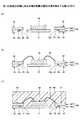
まず、第1の実施の形態に係る半導体装置の構造について説明する。図1は、第1の実施の形態に係る半導体装置を例示する図(その1)であり、図1(b)は底面図、図1(a)は図1(b)のA−A線に沿う断面図である。又、図2は、第1の実施の形態に係る半導体装置を例示する図(その2)であり、図2(a)は半導体装置全体を示す斜視図、図2(b)は上側リード及び下側リードを示す斜視図、図2(c)は上側リード及び下側リードを示す底面図である。<First Embodiment>
[Structure of Semiconductor Device According to First Embodiment]
First, the structure of the semiconductor device according to the first embodiment will be described. FIG. 1 is a diagram (part 1) illustrating the semiconductor device according to the first embodiment, in which FIG. 1 (b) is a bottom view and FIG. 1 (a) is an AA line in FIG. 1 (b). FIG. 2 is a diagram (part 2) illustrating the semiconductor device according to the first embodiment. FIG. 2 (a) is a perspective view showing the entire semiconductor device, and FIG. FIG. 2C is a perspective view showing the lower lead, and FIG. 2C is a bottom view showing the upper lead and the lower lead.
図1及び図2を参照するに、半導体装置1は、大略すると、リードフレーム10と、半導体チップ40と、金属線50(ボンディングワイヤ)と、樹脂部60とを有する。半導体装置1は、所謂QFNタイプの半導体装置である。 Referring to FIGS. 1 and 2, the
なお、本実施の形態では、便宜上、半導体装置1の第2フレーム30側を上側又は一方の側、第1フレーム20側を下側又は他方の側とする。又、各部位の第2フレーム30側の面を一方の面又は上面、第1フレーム20側の面を他方の面又は下面とする。但し、半導体装置1は天地逆の状態で用いることができ、又は任意の角度で配置することができる。又、平面視とは対象物を第1フレーム20の一方の面の法線方向から視ることを指し、平面形状とは対象物を第1フレーム20の一方の面の法線方向から視た形状を指すものとする。In the present embodiment, for convenience, the
半導体装置1において、リードフレーム10は、第1フレーム20の上面に第2フレーム30の下面を重ね合わせて溶接した構造とされている。第1フレーム20は、半導体チップが搭載されるチップ搭載部21(ダイパッド)と、複数の下側リード22(第1リード)とを備えている。第1フレーム20の材料としては、例えば、銅(Cu)や銅合金、42アロイ(FeとNiとの合金)等を用いることができる。 In the
下側リード22はチップ搭載部21と電気的に独立しており、平面視において、チップ搭載部21の周囲に所定のピッチで複数個設けられている。但し、下側リード22は必ずしもチップ搭載部21の周囲に設けなくてもよく、例えば、チップ搭載部21の両側に設けてもよい。下側リード22の幅は、例えば、0.2mm程度とすることができる。下側リード22のピッチは、例えば、0.4mm程度とすることができる。 The
下側リード22の下面の半導体チップ40側(リードの長手方向でチップ搭載部21に近い側)には、段差部22xが形成されている。言い換えれば、下側リード22の半導体チップ40側においては、上面側が下面側より長く形成されている。段差部22x以外の下側リード22の厚さは、例えば、75〜100μm程度とすることができる。段差部22xの部分の厚さは、段差部22x以外の下側リード22の厚さの半分程度とすることができる。 A
第2フレーム30は、金属線50と接続される複数の上側リード32(第2リード)を備えている。夫々の上側リード32は、平面視において、下側リード22と重複するように配置されている。第2フレーム30の材料としては、例えば、アルミニウム(Al)やアルミニウム合金、銅(Cu)や銅合金、42アロイ等を用いることができる。上側リード32の厚さは、例えば、75〜100μm程度とすることができる。なお、チップ搭載部21上には、第2フレーム30は配置されていない。 The
上側リード32の上面と下面の面積は略等しい。又、下側リード22の上面と下面(段差部22xも含む)の面積は略等しい。そして、下側リード22及び上側リード32の長手方向において、上側リード32の下面が下側リード22の上面よりも半導体チップ40側に延伸している。又、下側リード22及び上側リード32の短手方向において、上側リード32の下面が下側リード22の上面よりも両側に延伸している。 The area of the upper surface and the lower surface of the
言い換えれば、図2(c)に示すように、上側リード32の下面の面積は下側リード22の上面の面積よりも大きく、樹脂部60の側面から露出する側を除いて、底面視において、下側リード22の周囲に上側リード32の下面の外周部32aが露出している。外周部32aは、上側リード32の下面の下側リード22の上面よりも延伸した領域である。外周部32aは、樹脂部60により被覆されている。 In other words, as shown in FIG. 2C, the area of the lower surface of the
下側リード22と上側リード32とは、下側リード22の段差部22xに形成された接続部25により接合されている。具体的には、下側リード22の段差部22x内の一部を溶接して接続部25を形成し、上側リード32と接合している。接続部25以外の部分においては、下側リード22と上側リード32とは接しているだけであり、接合はされていない。段差部22xは、樹脂部60により被覆されている。 The
図1及び図2においては、便宜上、接続部25を下側リード22と区別して図示しているが、接続部25は下側リード22を局部的に溶融させた部分であり、下側リード22と同一材料により一体に構成されている。なお、下側リード22と上側リード32とが積層された部分を端子部と称する場合がある。つまり、下側リード22の上面に上側リード32の下面を重ね合わせて溶接し、端子部が形成されている。 In FIG. 1 and FIG. 2, for convenience, the
半導体チップ40は、第1フレーム20のチップ搭載部21上にフェイスアップ状態で搭載されている。半導体チップ40の上面側に形成された各電極端子は、第2フレーム30の各上側リード32と、金線や銅線等である金属線50を介して、電気的に接続(ワイヤボンディング)されている。金属線50は短い方がコスト的に有利であるため、上側リード32の下側リード22と平面視において重複しない領域に金属線50の一端を接続することが好ましい。 The
樹脂部60は、第1フレーム20、第2フレーム30、半導体チップ40、及び金属線50を封止している。但し、チップ搭載部21の下面、段差部22xを除く下側リード22の下面、下側リード22及び上側リード32の半導体装置1の外周縁部側の側面は、樹脂部60から露出している。すなわち、樹脂部60は、端子部の一部を露出するように半導体チップ40等を封止している。 The
チップ搭載部21の下面、及び段差部22xを除く下側リード22の下面は、樹脂部60の下面と略面一とすることができる。又、下側リード22及び上側リード32の半導体装置1の外周縁部側の側面は、樹脂部60の側面と略面一とすることができる。樹脂部60としては、例えば、エポキシ樹脂にフィラーを含有させた所謂モールド樹脂等を用いることができる。 The lower surface of the
[第1の実施の形態に係る半導体装置の製造方法]
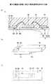
次に、第1の実施の形態に係る半導体装置の製造方法について説明する。図3〜図6は、第1の実施の形態に係る半導体装置の製造工程を例示する図である。[Method of Manufacturing Semiconductor Device According to First Embodiment]
Next, a method for manufacturing the semiconductor device according to the first embodiment will be described. 3 to 6 are diagrams illustrating the manufacturing process of the semiconductor device according to the first embodiment.
まず、図3に示す工程では、薄い金属板にプレス加工やエッチング加工等を施すことにより、第1フレーム20Sを形成する。第1フレーム20Sの材料としては、例えば、銅(Cu)や銅合金、42アロイ等を用いることができる。第1フレーム20Sの厚さは、例えば、75〜100μm程度とすることができる。なお、図3では、便宜上、第1フレーム20Sを梨地模様で示している。 First, in the process shown in FIG. 3, the
第1フレーム20Sは、枠部27により、破線で示す切断ラインで囲まれた領域C(以降、個片化領域Cと称する)が複数個(図3の例では8個)連結された構造を有する。個片化領域Cには、チップ搭載部21及び複数の下側リード22が形成されている。第1フレーム20Sは、最終的に破線で示す切断ラインに沿って切断されて個片化領域C毎に個片化され、複数の第1フレーム20(図1等参照)となる部材である。なお、第1フレーム20Sをプレス加工により形成した場合には、加工後に洗浄工程を設けることが好ましい。 The
次に、図4に示す工程では、薄い金属板にプレス加工やエッチング加工等を施すことにより、第2フレーム30Sを形成する。第2フレーム30Sの材料としては、例えば、アルミニウム(Al)やアルミニウム合金、銅(Cu)や銅合金、42アロイ等を用いることができる。第2フレーム30Sの厚さは、例えば、75〜100μm程度とすることができる。なお、図4では、便宜上、第2フレーム30Sを梨地模様で示している。Next, in the process shown in FIG. 4, the
第2フレーム30Sは、枠部37により、破線で示す切断ラインで囲まれた領域C(以降、個片化領域Cと称する)が複数個(図4の例では8個)連結された構造を有する。個片化領域Cには、複数の上側リード32が形成されている。第2フレーム30Sは、最終的に破線で示す切断ラインに沿って切断されて個片化領域C毎に個片化され、複数の第2フレーム30(図1等参照)となる部材である。なお、第2フレーム30Sをプレス加工により形成した場合には、加工後に洗浄工程を設けることが好ましい。以降の工程については、図3及び図4に示した個片化領域Cに対応する断面図を用いて説明する。 The
次に、図5(a)に示す工程では、図3に示す工程で作製した第1フレーム20Sを加工して、下側リード22の下面の内縁側(リードの長手方向でチップ搭載部21に近い側)に段差部22xを形成する。段差部22xの部分の厚さは、段差部22x以外の下側リード22の厚さの半分程度とすることができる。段差部22xは、例えば、ウェットエッチングにより形成できる。但し、段差部22xの深さによっては、図3の工程で金属板にプレス加工して、チップ搭載部21及び下側リード22と同時に段差部22xを形成することも可能である。その場合には、図5(a)に示す工程は不要となる。 Next, in the process shown in FIG. 5A, the
次に、図5(b)に示す工程では、段差部22xが形成された第1フレーム20Sの上面に、図4に示す工程で作製した第2フレーム30Sの下面を重ね合わせる。ここで、上側リード32の下面の面積は下側リード22の上面の面積よりも大きく形成されているため、個片化領域Cの外周側を除いて、底面視において、下側リード22の周囲に上側リード32の下面の外周部32aが露出する(図2(c)参照)。外周部32aは、上側リード32の下面の下側リード22の上面よりも延伸した領域である。 Next, in the step shown in FIG. 5B, the lower surface of the
次に、図5(c)に示す工程では、第1フレーム20Sの下側リード22と第2フレーム30Sの上側リード32とを接続部25により接合する。具体的には、段差部22xにレーザ光を照射して下側リード22を構成する金属材料を局部的に溶融させて接続部25を形成し、下側リード22と上側リード32とを接合する(レーザ溶接)。これにより、下側リード22の上面に上側リード32の下面を重ね合わせて溶接した構造の端子部が作製される。レーザ光としては、例えば、第2高調波(SHG)を用いたグリーンレーザ等を用いることができる。この場合、レーザ光の波長は、例えば、532nm程度とすることができる。 Next, in the step shown in FIG. 5C, the
以上の工程により、第1フレーム20S及び第2フレーム30Sを有するリードフレーム10Sが作製される。なお、リードフレーム10Sは、最終的に図3及び図4に示す破線で示す切断ラインに沿って切断されて個片化領域C毎に個片化され、複数のリードフレーム10(図1等参照)となる部材である。 Through the above steps, the
次に、図6(a)に示す工程では、第1フレーム20Sのチップ搭載部21上に半導体チップ40をフェイスアップ状態で搭載する。半導体チップ40は、例えば、ダイアタッチフィルムを介してチップ搭載部21上に搭載することができる。 Next, in the process shown in FIG. 6A, the
次に、図6(b)に示す工程では、半導体チップ40の上面側に形成された電極端子を、金属線50を介して、上側リード32と電気的に接続する。金属線50は、例えば、ワイヤボンディングにより、半導体チップ40の電極端子及び上側リード32と接続できる。 Next, in the step shown in FIG. 6B, the electrode terminal formed on the upper surface side of the
次に、図6(c)に示す工程では、第1フレーム20S、第2フレーム30S、半導体チップ40、及び金属線50を封止する樹脂部60を形成する。樹脂部60としては、例えば、エポキシ樹脂にフィラーを含有させた所謂モールド樹脂等を用いることができる。樹脂部60は、例えば、トランスファーモールド法やコンプレッションモールド法等により形成できる。 Next, in the step shown in FIG. 6C, the
その後、図6(c)に示す構造体を、図3及び図4に破線で示した切断ラインに沿って切断し、個片化領域C毎に個片化することにより、複数の半導体装置1(図1参照)が完成する。切断は、例えば、スライサー等により実行できる。なお、第1フレーム20Sの枠部27及び第2フレーム30Sの枠部37の夫々のダムバーは、切断ラインに沿って同時に切断することができる。 After that, the structure shown in FIG. 6C is cut along the cutting lines shown by the broken lines in FIGS. 3 and 4 and separated into individual pieces C, whereby a plurality of
第1フレーム20Sの枠部27及び第2フレーム30Sの枠部37を共に切断ラインの外側に配置し、個片化時に同時に切断除去することで効率的に製造することができる。このような製造方法を採用するため、樹脂部60の側面には下側リード22及び上側リード32の端面が露出した構造となる。Theframe portion 27 of the
以上、半導体装置1を1つの製品として出荷する際の製造工程について説明したが、図5(c)に示す個片化前のリードフレーム10Sを1つの製品として出荷してもよい。この場合には、個片化前のリードフレーム10Sを製品として入手した者が図6(a)以降の工程を実行し、複数の半導体装置1を作製することができる。 The manufacturing process for shipping the
このように、第1の実施の形態では、下側リード22と上側リード32とを別々に作製し、レーザ溶接等により形成した接続部25により両者を強固に接合して端子部としている。又、平面視において下側リード22を上側リード32よりも小さくする(小面積にする)ことにより、樹脂部60の側面から露出する側を除いて、端子部において上側リード32の下面が延伸して下側リード22の周囲に外周部32aが露出している。これにより、外周部32aに樹脂部60を構成する樹脂が回り込むため、外周部32aと樹脂部60との間にアンカー効果が生じ、端子部と樹脂部60との密着性を向上できる。これにより、樹脂部60を構成する樹脂の剥がれや、端子部の脱落を防止できる。 As described above, in the first embodiment, the
又、下側リード22に形成された段差部22xは樹脂部60に被覆され、半導体装置1の外部には露出しない。つまり、段差部22xにも樹脂部60を構成する樹脂が回り込む構造であるため、段差部22xと樹脂部60との間にもアンカー効果が生じ、端子部と樹脂部60との密着性を更に向上できる。これにより、樹脂部60を構成する樹脂の剥がれや、下側リード22の脱落を防止できる。 Further, the
又、下側リード22の少なくとも側面を粗化面としておくことで、下側リード22と樹脂部60との密着性が向上し、下側リード22の脱落を防止できる。同様の理由で、チップ搭載部21(ダイパッド)の少なくとも側面が粗化された構造であってもよい。 In addition, by providing at least the side surface of the
又、加工精度の低いハーフエッチングを用いずに、低コストで高精度の加工が可能なプレス加工等により下側リード22及び上側リード32を別々に形成し、その後、下側リード22及び上側リード32を上下に積層して端子部を形成している。そのため、端子部を微細化することが可能となり、端子部の狭ピッチ化及び多ピン化を実現できる。又、ハーフエッチングを用いた場合と比較して、加工コストを低減できる。 In addition, the
又、下側リード22と上側リード32とに異なる金属材料を用いることにより、夫々の金属材料の特徴を生かした効果を得ることができる。例えば、下側リード22に銅(Cu)を用いることにより、はんだめっきが可能となり、又、上側リード32にアルミニウム(Al)を用いることにより、ワイヤボンディングする領域のめっきレス化が可能となる。 Further, by using different metal materials for the
〈第1の実施の形態の変形例〉
第1の実施の形態の変形例では、リードフレームの一部にめっきを施す例を示す。なお、第1の実施の形態の変形例において、既に説明した実施の形態と同一構成部についての説明は省略する場合がある。<Modification of First Embodiment>
In the modification of the first embodiment, an example in which a part of the lead frame is plated is shown. In the modification of the first embodiment, the description of the same components as those of the already described embodiments may be omitted.
図7は、第1の実施の形態の変形例に係る半導体装置を例示する断面図である。図7(a)に示す半導体装置1Aでは、第2フレーム30の上側リード32の金属線50と接合される領域にめっき膜33を形成している。例えば、上側リード32がアルミニウム(Al)やアルミニウム合金からなる場合には、めっき膜を形成しなくても良好なボンディングが実施可能である。一方、上側リード32が銅(Cu)や銅合金、42アロイからなる場合には、直接ボンディングを行うことが困難である。このような場合には、めっき膜33を形成することにより、良好なボンディングが実施可能となる。 FIG. 7 is a cross-sectional view illustrating a semiconductor device according to a variation of the first embodiment. In the
めっき膜33としては、例えば、Au膜やAg膜、Ni/Au膜(Ni膜とAu膜をこの順番で積膜した金属膜)、Ni/Pd/Au膜(Ni膜とPd膜とAu膜をこの順番で積膜した金属膜)等を挙げることができる。めっき膜33の厚さは、例えば、0.1〜数μm程度とすることができる。めっき膜33は、例えば、電解めっき法により形成することができる。なお、必要に応じ、めっき膜33を形成する前に、上側リード32の上面に粗化処理を施してもよい。上側リード32の上面に粗化処理を施すことにより、上側リード32の上面とめっき膜33との密着性を向上できる。 Examples of the
図7(b)に示す半導体装置1Bでは、めっき膜33に加え、樹脂部60から露出する第1フレーム20の下側リード22の下面及びチップ搭載部21の下面にめっき膜23を形成している。めっき膜23を形成することにより、半導体装置1Bを他の配線基板等と接合する際に、良好な接合が可能となる。めっき膜23の材料や形成方法は、めっき膜33と同様とすることができる。 In the
このように、必要に応じて、下側リード22や上側リード32の所定の面に、めっき膜を形成してもよい。半導体装置1A及び1Bにおいて、その他の効果については、第1の実施の形態と同様である。 Thus, a plating film may be formed on a predetermined surface of the
〈第2の実施の形態〉
第2の実施の形態では、上側リードにも接続部を形成する例を示す。なお、第2の実施の形態において、既に説明した実施の形態と同一構成部についての説明は省略する場合がある。<Second Embodiment>
In the second embodiment, an example in which a connection portion is formed also on the upper lead is shown. In the second embodiment, description of the same components as those of the already described embodiments may be omitted.
図8は、第2の実施の形態に係る半導体装置を例示する図であり、図8(a)は半導体装置全体を示す断面図、図8(b)は上側リード及び下側リードを示す斜視図、図8(c)は上側リード及び下側リードを示す平面図である。 FIG. 8 is a diagram illustrating a semiconductor device according to the second embodiment. FIG. 8A is a cross-sectional view showing the entire semiconductor device, and FIG. 8B is a perspective view showing an upper lead and a lower lead. FIG. 8C is a plan view showing the upper lead and the lower lead.
図8を参照するに、半導体装置2では、半導体装置1と同様に、下側リード22の下面の内縁側(リードの長手方向でチップ搭載部21に近い側)に段差部22xが形成されており、下側リード22と上側リード32とは段差部22xに形成された接続部25により接合されている。それに加え、半導体装置2では、半導体装置1とは異なり、下側リード22と上側リード32とは、上側リード32の外縁側(リードの長手方向でチップ搭載部21から遠い側)に形成された第2接続部35によっても接合されている。 Referring to FIG. 8, in the
第2接続部35は、接続部25と同様に、レーザ溶接により形成することができる。なお、図8においては、便宜上、第2接続部35を上側リード32と区別して図示しているが、第2接続部35は上側リード32を局部的に溶融させた部分であり、上側リード32と同一材料により一体に構成されている。 Similar to the
このように、下側リード22と上側リード32とを内縁側(リードの長手方向でチップ搭載部21に近い側)の接続部25に加え、外縁側(リードの長手方向でチップ搭載部21から遠い側)の第2接続部35でも接合する。これにより、半導体装置2の外周側面に近い部分においても下側リード22と上側リード32とが強固に接合される。そのため、半導体装置2の外周側面に露出する下側リード22と上側リード32との界面から水分等が侵入することを効果的に抑制できる。その他の効果については、第1の実施の形態と同様である。 In this way, the
〈第3の実施の形態〉
第3の実施の形態では、上側リードに段差部を形成し、上側リードの段差部にも接続部を形成する例を示す。なお、第3の実施の形態において、既に説明した実施の形態と同一構成部についての説明は省略する場合がある。<Third Embodiment>
In the third embodiment, an example in which a step portion is formed on the upper lead and a connection portion is also formed on the step portion of the upper lead is shown. Note that in the third embodiment, description of the same components as those of the already described embodiments may be omitted.
図9は、第3の実施の形態に係る半導体装置を例示する図であり、図9(a)は半導体装置全体を示す断面図、図9(b)は上側リード及び下側リードを示す斜視図、図9(c)は上側リード及び下側リードを示す平面図である。 FIG. 9 is a diagram illustrating a semiconductor device according to the third embodiment. FIG. 9A is a cross-sectional view showing the entire semiconductor device, and FIG. 9B is a perspective view showing an upper lead and a lower lead. FIG. 9C is a plan view showing the upper lead and the lower lead.
図9を参照するに、半導体装置3では、半導体装置1と同様に、下側リード22の下面の内縁側(リードの長手方向でチップ搭載部21に近い側)に段差部22xが形成されており、下側リード22と上側リード32とは段差部22xに形成された接続部25により接合されている。それに加え、半導体装置3では、半導体装置1とは異なり、上側リード32の上面の外縁側(リードの長手方向でチップ搭載部21から遠い側)に第2段差部32yが形成されている。そして、下側リード22と上側リード32とは第2段差部32yに形成された第2接続部35によっても接合されている。第2段差部32yは、樹脂部60により被覆されている。 Referring to FIG. 9, in the semiconductor device 3, similarly to the
第2接続部35は、接続部25と同様に、レーザ溶接により形成することができる。なお、図9においては、便宜上、第2接続部35を上側リード32と区別して図示しているが、第2接続部35は上側リード32を局部的に溶融させた部分であり、上側リード32と同一材料により一体に構成されている。 Similar to the
このように、下側リード22と上側リード32とを内縁側(リードの長手方向でチップ搭載部21に近い側)の接続部25に加え、外縁側(リードの長手方向でチップ搭載部21から遠い側)の第2接続部35でも接合する。これにより、半導体装置3の外周側面に近い部分においても下側リード22と上側リード32とが強固に接合される。そのため、半導体装置3の外周側面に露出する下側リード22と上側リード32との界面から水分等が侵入することを効果的に抑制できる。 In this way, the
又、図8に示す半導体装置2と比べて、第2接続部35を形成するためにレーザ溶接する部分の厚さが薄いため(第2段差部32yに第2接続部35を形成するため)、効率的な局部加熱が可能となり、レーザ溶接の工程を短縮化できる。その他の効果については、第1の実施の形態と同様である。 Further, the thickness of the portion to be laser-welded to form the
〈第4の実施の形態〉
第4の実施の形態では、下側リードに2つの段差部を形成する例を示す。なお、第4の実施の形態において、既に説明した実施の形態と同一構成部についての説明は省略する場合がある。<Fourth embodiment>
The fourth embodiment shows an example in which two step portions are formed on the lower lead. Note that in the fourth embodiment, descriptions of the same components as those of the above-described embodiments may be omitted.
図10は、第4の実施の形態に係る半導体装置を例示する図(その1)であり、図10(b)は底面図、図10(a)は図10(b)のA−A線に沿う断面図である。又、図11は、第4の実施の形態に係る半導体装置を例示する図(その2)であり、図11(a)は半導体装置全体を示す斜視図、図11(b)は上側リード及び下側リードを示す斜視図、図11(c)は上側リード及び下側リードを示す底面図である。 FIG. 10 is a diagram (part 1) illustrating the semiconductor device according to the fourth embodiment, in which FIG. 10 (b) is a bottom view, and FIG. 10 (a) is an AA line in FIG. 10 (b). FIG. FIG. 11 is a diagram (part 2) illustrating the semiconductor device according to the fourth embodiment. FIG. 11A is a perspective view showing the entire semiconductor device, and FIG. FIG. 11C is a perspective view showing the lower lead, and FIG. 11C is a bottom view showing the upper lead and the lower lead.
図10及び図11を参照するに、半導体装置4では、半導体装置1と同様に、下側リード22の下面の内縁側(リードの長手方向でチップ搭載部21に近い側)に段差部22xが形成されており、下側リード22と上側リード32とは段差部22xに形成された接続部25により接合されている。それに加え、半導体装置4では、半導体装置1とは異なり、下側リード22の下面の外縁側(リードの長手方向でチップ搭載部21から遠い側)に第3段差部22yが形成されている。そして、下側リード22と上側リード32とは第3段差部22yに形成された第3接続部26によっても接合されている。第3段差部22yは、樹脂部60により被覆されている。 Referring to FIGS. 10 and 11, in the
第3接続部26は、接続部25と同様に、レーザ溶接により形成することができる。なお、図10及び図11においては、便宜上、第3接続部26を下側リード22と区別して図示しているが、第3接続部26は下側リード22を局部的に溶融させた部分であり、下側リード22と同一材料により一体に構成されている。 The
このように、下側リード22と上側リード32とを内縁側(リードの長手方向でチップ搭載部21に近い側)の接続部25に加え、外縁側(リードの長手方向でチップ搭載部21から遠い側)の第3接続部26で接合する。これにより、半導体装置4の外周側面に近い部分においても下側リード22と上側リード32とが強固に接合される。そのため、半導体装置4の外周側面に露出する下側リード22と上側リード32との界面から水分等が侵入することを効果的に抑制できる。 In this way, the
又、下側リード22に第3段差部22yを形成し、第3段差部22yは樹脂部60に被覆され、半導体装置4の外部には露出しない。つまり、第3段差部22yにも樹脂部60を構成する樹脂が回り込む構造であるため、第3段差部22yと樹脂部60との間にもアンカー効果が生じ、端子部と樹脂部60との密着性を更に向上できる。これにより、樹脂部60を構成する樹脂の剥がれや、下側リード22の脱落を防止できる。 Further, a
又、第3接続部26を形成するためにレーザ溶接する部分の厚さが薄いため(第3段差部22yに第3接続部26を形成するため)、効率的な局部加熱が可能となり、レーザ溶接の工程を短縮化できる。その他の効果については、第1の実施の形態と同様である。 Further, since the thickness of the portion to be laser-welded to form the
〈第5の実施の形態〉
第5実施の形態では、下側リードに段差部を形成しない例を示す。なお、第5の実施の形態において、既に説明した実施の形態と同一構成部についての説明は省略する場合がある。<Fifth embodiment>
In the fifth embodiment, an example in which a step portion is not formed on the lower lead is shown. Note that in the fifth embodiment, description of the same components as those of the above-described embodiments may be omitted.
図12は、第5の実施の形態に係る半導体装置を例示する図であり、図12(a)は半導体装置全体を示す断面図、図12(b)は上側リード及び下側リードを示す斜視図、図12(c)は上側リード及び下側リードを示す底面図である。 12A and 12B are diagrams illustrating a semiconductor device according to the fifth embodiment. FIG. 12A is a cross-sectional view showing the entire semiconductor device, and FIG. 12B is a perspective view showing an upper lead and a lower lead. FIG. 12C is a bottom view showing the upper lead and the lower lead.
図12を参照するに、半導体装置5では、半導体装置1とは異なり、下側リード22に段差部22xが形成されていない。下側リード22と上側リード32とは下側リード22の内縁側(リードの長手方向でチップ搭載部21に近い側)に形成された接続部25によって接合されている。 Referring to FIG. 12, in the semiconductor device 5, unlike the
このように、下側リード22に段差部22xを形成せず、下側リード22と上側リード32とを下側リード22の内縁側(リードの長手方向でチップ搭載部21に近い側)に形成された接続部25によって接合してもよい。この場合にも、端子部において上側リード32の下面が延伸して下側リード22の周囲に外周部32aが露出している。これにより、外周部32aに樹脂部60を構成する樹脂が回り込むため、外周部32aと樹脂部60との間にアンカー効果が生じ、端子部と樹脂部60との密着性を向上できる。これにより、樹脂部60を構成する樹脂の剥がれや、端子部の脱落を防止できる。 In this way, the
又、加工精度の低いハーフエッチングを用いずに、低コストで高精度の加工が可能なプレス加工等により下側リード22及び上側リード32を別々に形成し、その後、下側リード22及び上側リード32を上下に積層して端子部を形成している。そのため、端子部を微細化することが可能となり、端子部の狭ピッチ化及び多ピン化を実現できる。又、ハーフエッチングを用いた場合と比較して、加工コストを低減できる。 In addition, the
又、下側リード22と上側リード32とに異なる金属材料を用いることにより、夫々の金属材料の特徴を生かした効果を得ることができる。例えば、下側リード22に銅(Cu)を用いることにより、はんだめっきが可能となり、又、上側リード32にアルミニウム(Al)を用いることにより、ワイヤボンディングする領域のめっきレス化が可能となる。 Further, by using different metal materials for the
〈第6の実施の形態〉
第6実施の形態では、チップ搭載部に段差部を形成する例を示す。なお、第6の実施の形態において、既に説明した実施の形態と同一構成部についての説明は省略する場合がある。<Sixth embodiment>
In the sixth embodiment, an example in which a step portion is formed in the chip mounting portion will be described. Note that in the sixth embodiment, descriptions of the same components as in the already described embodiments may be omitted.
図13は、第6の実施の形態に係る半導体装置を例示する断面図である。図13を参照するに、半導体装置6では、半導体装置1とは異なり、チップ搭載部21の下面の外周側に第4段差部21xが形成されている。第4段差部21xは、例えば、チップ搭載部21の下面の外周側に額縁状に形成することができる。 FIG. 13 is a cross-sectional view illustrating a semiconductor device according to the sixth embodiment. Referring to FIG. 13, in the semiconductor device 6, unlike the
このように、チップ搭載部21の下面の外周側に第4段差部21xが形成されてもよい。これにより、第4段差部21xに樹脂部60を構成する樹脂が回り込むため、第4段差部21xと樹脂部60との間にアンカー効果が生じ、チップ搭載部21と樹脂部60との密着性を向上できる。これにより、樹脂部60を構成する樹脂の剥がれや、チップ搭載部21の脱落を防止できる。その他の効果については、第1の実施の形態と同様である。 As described above, the
以上、好ましい実施の形態及び変形例について詳説したが、上述した実施の形態及び変形例に制限されることはなく、特許請求の範囲に記載された範囲を逸脱することなく、上述した実施の形態及び変形例に種々の変形及び置換を加えることができる。 The preferred embodiment and the modification have been described in detail above. However, the present invention is not limited to the embodiment and the modification described above, and the embodiment described above without departing from the scope described in the claims. Various modifications and substitutions can be made to the modification examples.
例えば、上記実施の形態及び変形例では、第1フレーム20がチップ搭載部(ダイパッド)を備える例を示したが、第2フレーム30がチップ搭載部を備える構造としてもよい。或いは、第1フレーム20及び第2フレームがチップ搭載部を備え、夫々のチップ搭載部を積層して溶接により接合した構造としてもよい。 For example, in the above-described embodiment and modification, the example in which the
又、チップ搭載部(ダイパッド)は樹脂部から露出しなくてもよい。 Further, the chip mounting portion (die pad) may not be exposed from the resin portion.
又、接続部はリードの外縁側や内縁側だけでなく、任意の箇所に形成することができる。又、段差部も同様に、任意の箇所に形成することができる。 Further, the connecting portion can be formed not only at the outer edge side and the inner edge side of the lead but also at an arbitrary place. Similarly, the step portion can be formed at an arbitrary location.
又、各実施の形態や変形例は適宜組み合わせることができる。 Moreover, each embodiment and modification can be combined suitably.
1、1A、1B、2、3、4、5、6 半導体装置
10、10S リードフレーム
20、20S 第1フレーム
21 チップ搭載部
21x 第4段差部
22 下側リード
22x 段差部
22y 第3段差部
23、33 めっき膜
25 接続部
26 第3接続部
27、37 枠部
30、30S 第2フレーム
32 上側リード
32a 上側リードの下面の外周部
32y 第2段差部
35 第2接続部
40 半導体チップ
50 金属線
60 樹脂部1, 1A, 1B, 2, 3, 4, 5, 6
Claims (8)
Translated fromJapanese前記端子部と電気的に接続された半導体チップと、
前記端子部の一部を露出するように前記半導体チップを封止する樹脂部と、を有し、
前記端子部は、第1リードの上面に第2リードの下面を重ね合わせて溶接した構造であり、
前記端子部の長手方向において前記第2リードの下面が前記第1リードの上面よりも前記半導体チップ側に延伸し、かつ、前記端子部の短手方向において前記第2リードの下面が前記第1リードの上面よりも両側に延伸し、
前記第1リードの下面の前記半導体チップ側に段差部が形成され、
前記段差部に、前記第2リードと溶接された接続部が形成され、
前記第2リードの下面の前記第1リードの上面よりも延伸した領域及び前記段差部は、前記樹脂部により被覆されている半導体装置。A lead frame with a terminal portion;
A semiconductor chip electrically connected to the terminal portion;
A resin part for sealing the semiconductor chip so as to expose a part of the terminal part,
The terminal portion has a structure in which the lower surface of the second lead is overlapped and welded to the upper surface of the first lead.
In the longitudinal direction of the terminal portion, the lower surface of the second lead extends to the semiconductor chip side from the upper surface of the first lead, and the lower surface of the second lead in the shorter direction of the terminal portion is the first. Extends on both sides of the top of the lead,
A step portion is formed on the semiconductor chip side of the lower surface of the first lead,
A connection portion welded to the second lead is formed on the stepped portion,
An area of the lower surface of the second lead extending from the upper surface of the first leadand the stepped portion are covered with the resin portion.
前記第2段差部に前記第2接続部が形成され、
前記第2段差部は前記樹脂部により被覆されている請求項2記載の半導体装置。A second stepped portion is formed on the opposite side of the upper surface of the second lead from the semiconductor chip side;
The second connecting portion is formed on the second stepped portion;
The second step portion semiconductor device according to claim2, characterized in that is coated with the resin portion.
前記第3段差部に、前記第2リードと溶接された第3接続部が形成され、
前記第3段差部は、前記樹脂部により被覆されている請求項1乃至3の何れか一項記載の半導体装置。A third step portion is formed on the opposite side of the lower surface of the first lead to the semiconductor chip side;
The third stepportion, a third connecting portionwhich is welded to thefront Stories second leads are formed,
The third step portion, the semiconductor device of any one of claims1 to3 are covered with the resin portion.
前記領域の各々は端子部を有し、
前記端子部は、第1リードの上面に第2リードの下面を重ね合わせて溶接した構造であり、
前記端子部の長手方向において前記第2リードの下面が前記第1リードの上面よりも前記領域の中心側に延伸し、かつ、前記端子部の短手方向において前記第2リードの下面が前記第1リードの上面よりも両側に延伸し、
前記第1リードの下面の前記中心側に段差部が形成され、
前記段差部に、前記第2リードと溶接された接続部が形成されているリードフレーム。It has a plurality of areas to be singulated,
Each of the regions has a terminal portion;
The terminal portion has a structure in which the lower surface of the second lead is overlapped and welded to the upper surface of the first lead.
In the longitudinal direction of the terminal portion, the lower surface of the second lead extends toward the center of the region from the upper surface of the first lead, and the lower surface of the second lead extends in the short direction of the terminal portion. 1 lead to both sides than the top of the lead,
A step portion is formed on the center side of the lower surface of the first lead,
A lead framein which a connection portion welded to the second lead is formed in the stepped portion .
前記第2段差部に前記第2接続部が形成されている請求項6記載のリードフレーム。A second step is formed on the opposite side of the upper surface of the second lead from the center side;
The lead frame according to claim6 , wherein the second connection portion is formed in the second step portion.
前記第3段差部に、前記第2リードと溶接された第3接続部が形成されている請求項5乃至7の何れか一項記載のリードフレーム。A third step portion is formed on the opposite side of the lower surface of the first lead from the center side;
The thirdstep portion, the lead framebefore SL any one claim of the third connection requesting unit is formed to claim5 to7, which is welded to the second lead.
Priority Applications (5)
| Application Number | Priority Date | Filing Date | Title |
|---|---|---|---|
| JP2014257463AJP6325975B2 (en) | 2014-12-19 | 2014-12-19 | Lead frame, semiconductor device |
| KR1020150164526AKR102452097B1 (en) | 2014-12-19 | 2015-11-24 | Lead frame and semi-conductor device |
| US14/955,117US9698084B2 (en) | 2014-12-19 | 2015-12-01 | Semiconductor device and lead frame having two leads welded together |
| TW104140272ATWI668826B (en) | 2014-12-19 | 2015-12-02 | Lead frame, semiconductor device |
| CN201510882130.7ACN105720034B (en) | 2014-12-19 | 2015-12-03 | Lead frame, semiconductor device |
Applications Claiming Priority (1)
| Application Number | Priority Date | Filing Date | Title |
|---|---|---|---|
| JP2014257463AJP6325975B2 (en) | 2014-12-19 | 2014-12-19 | Lead frame, semiconductor device |
Publications (3)
| Publication Number | Publication Date |
|---|---|
| JP2016119366A JP2016119366A (en) | 2016-06-30 |
| JP2016119366A5 JP2016119366A5 (en) | 2017-08-31 |
| JP6325975B2true JP6325975B2 (en) | 2018-05-16 |
Family
ID=56130317
Family Applications (1)
| Application Number | Title | Priority Date | Filing Date |
|---|---|---|---|
| JP2014257463AActiveJP6325975B2 (en) | 2014-12-19 | 2014-12-19 | Lead frame, semiconductor device |
Country Status (5)
| Country | Link |
|---|---|
| US (1) | US9698084B2 (en) |
| JP (1) | JP6325975B2 (en) |
| KR (1) | KR102452097B1 (en) |
| CN (1) | CN105720034B (en) |
| TW (1) | TWI668826B (en) |
Families Citing this family (12)
| Publication number | Priority date | Publication date | Assignee | Title |
|---|---|---|---|---|
| JP6325975B2 (en)* | 2014-12-19 | 2018-05-16 | 新光電気工業株式会社 | Lead frame, semiconductor device |
| JP6577373B2 (en)* | 2016-01-18 | 2019-09-18 | 新光電気工業株式会社 | Lead frame, manufacturing method thereof, and semiconductor device |
| JP6788509B2 (en)* | 2017-01-17 | 2020-11-25 | 株式会社三井ハイテック | Lead frame manufacturing method and lead frame |
| JP6661565B2 (en)* | 2017-03-21 | 2020-03-11 | 株式会社東芝 | Semiconductor device and manufacturing method thereof |
| DE102017120747B4 (en)* | 2017-09-08 | 2020-07-30 | Infineon Technologies Austria Ag | Top cooling SMD package and method of providing it |
| RU180407U1 (en)* | 2018-02-06 | 2018-06-13 | Закрытое акционерное общество "ГРУППА КРЕМНИЙ ЭЛ" | OUTPUT FRAME OF THE INTEGRAL IC |
| DE102018217659B4 (en) | 2018-10-15 | 2022-08-04 | Vitesco Technologies GmbH | Arrangement and method for producing an electrically conductive connection between two substrates |
| JP7271337B2 (en) | 2019-06-27 | 2023-05-11 | 新光電気工業株式会社 | Electronic component device and method for manufacturing electronic component device |
| JP7467214B2 (en)* | 2020-04-22 | 2024-04-15 | 新光電気工業株式会社 | Wiring board, electronic device, and method for manufacturing wiring board |
| KR102514564B1 (en)* | 2021-06-28 | 2023-03-29 | 해성디에스 주식회사 | Lead frame including grooved lead |
| JP2023030665A (en)* | 2021-08-23 | 2023-03-08 | 株式会社ディスコ | Package substrate, method for processing package substrate, and package chip |
| CN114121853B (en)* | 2022-01-27 | 2022-05-24 | 深圳中科四合科技有限公司 | Packaging structure of large-size chip adaptive small-size packaging body |
Family Cites Families (16)
| Publication number | Priority date | Publication date | Assignee | Title |
|---|---|---|---|---|
| AU2001272814A1 (en)* | 2000-07-25 | 2002-02-05 | Chan-Ik Park | Plastic package base, air cavity type package and their manufacturing methods |
| KR100335658B1 (en)* | 2000-07-25 | 2002-05-06 | 장석규 | Base of plastic package and method of manufacturing the same |
| SG102638A1 (en)* | 2000-09-15 | 2004-03-26 | Samsung Techwin Co Ltd | Lead frame, semiconductor package having the same, and semiconductor package manufacturing method |
| JP3691790B2 (en) | 2001-12-27 | 2005-09-07 | 株式会社三井ハイテック | Semiconductor device manufacturing method and semiconductor device manufactured by the method |
| KR20060021744A (en)* | 2004-09-04 | 2006-03-08 | 삼성테크윈 주식회사 | Lead frame and manufacturing method |
| JP4196937B2 (en)* | 2004-11-22 | 2008-12-17 | パナソニック株式会社 | Optical device |
| US7352058B2 (en)* | 2005-11-01 | 2008-04-01 | Sandisk Corporation | Methods for a multiple die integrated circuit package |
| CN101794760B (en)* | 2006-10-06 | 2012-05-23 | 万国半导体股份有限公司 | Low profile integrated circuit package for high current semiconductor power devices |
| US7622793B2 (en)* | 2006-12-21 | 2009-11-24 | Anderson Richard A | Flip chip shielded RF I/O land grid array package |
| JP5343334B2 (en)* | 2007-07-17 | 2013-11-13 | 株式会社デンソー | Welded structure and manufacturing method thereof |
| WO2009081723A1 (en)* | 2007-12-20 | 2009-07-02 | Fuji Electric Device Technology Co., Ltd. | Semiconductor device and method for manufacturing the same |
| CN101383293B (en)* | 2008-09-26 | 2010-08-04 | 凤凰半导体通信(苏州)有限公司 | Micro lead frame semiconductor packaging method |
| JP2010263094A (en)* | 2009-05-08 | 2010-11-18 | Hitachi Metals Ltd | Lead frame |
| MY155671A (en)* | 2010-01-29 | 2015-11-13 | Toshiba Kk | LED package and method for manufacturing same |
| US20150206830A1 (en)* | 2012-09-24 | 2015-07-23 | Renesas Electronics Corporation | Method Of Manufacturing Semiconductor Device And The Semiconductor Device |
| JP6325975B2 (en)* | 2014-12-19 | 2018-05-16 | 新光電気工業株式会社 | Lead frame, semiconductor device |
- 2014
- 2014-12-19JPJP2014257463Apatent/JP6325975B2/enactiveActive
- 2015
- 2015-11-24KRKR1020150164526Apatent/KR102452097B1/enactiveActive
- 2015-12-01USUS14/955,117patent/US9698084B2/enactiveActive
- 2015-12-02TWTW104140272Apatent/TWI668826B/enactive
- 2015-12-03CNCN201510882130.7Apatent/CN105720034B/enactiveActive
Also Published As
| Publication number | Publication date |
|---|---|
| KR102452097B1 (en) | 2022-10-11 |
| CN105720034B (en) | 2019-07-05 |
| KR20160075316A (en) | 2016-06-29 |
| CN105720034A (en) | 2016-06-29 |
| US9698084B2 (en) | 2017-07-04 |
| US20160181187A1 (en) | 2016-06-23 |
| JP2016119366A (en) | 2016-06-30 |
| TW201624658A (en) | 2016-07-01 |
| TWI668826B (en) | 2019-08-11 |
Similar Documents
| Publication | Publication Date | Title |
|---|---|---|
| JP6325975B2 (en) | Lead frame, semiconductor device | |
| US9905497B2 (en) | Resin sealing type semiconductor device and method of manufacturing the same, and lead frame | |
| JP6244147B2 (en) | Manufacturing method of semiconductor device | |
| US8853841B2 (en) | Lead frame which includes terminal portion having through groove covered by lid portion, semiconductor package, and manufacturing method of the same | |
| JP6555927B2 (en) | Semiconductor device mounting lead frame and semiconductor device manufacturing method | |
| JP6653139B2 (en) | Lead frame and manufacturing method thereof | |
| HK1208957A1 (en) | Manufacturing method of semiconductor device and semiconductor device | |
| JP2014007363A (en) | Method of manufacturing semiconductor device and semiconductor device | |
| TWI624883B (en) | Method of manufacturing resin-encapsulated semiconductor device, and resin-encapsulated semiconductor device | |
| JP2019021815A (en) | Semiconductor device mounting substrate and manufacturing method thereof | |
| JP7182374B2 (en) | Lead frame and manufacturing method thereof | |
| JP2014007287A (en) | Semiconductor device manufacturing method | |
| JP2019057587A (en) | Substrate for mounting semiconductor element thereon and method of manufacturing the same | |
| JP2019121698A (en) | Semiconductor device and method for manufacturing semiconductor device | |
| JP2018085487A (en) | Semiconductor device manufacturing method and semiconductor device | |
| JP7674930B2 (en) | Lead frame, semiconductor device, and method of manufacturing lead frame | |
| JP2017163106A (en) | Lead frame assembly substrate and semiconductor device assembly | |
| JP2017038051A (en) | Semiconductor package and manufacturing method thereof | |
| KR20240043156A (en) | Semiconductor device and manufacturing method thereof | |
| JP2017135335A (en) | Lead frame and semiconductor device, and method of manufacturing them | |
| JP5104020B2 (en) | Mold package | |
| CN211404492U (en) | Visual angle lead frame structure with circuit tin absorption | |
| JP2002164496A (en) | Semiconductor device and manufacturing method thereof | |
| JP7145414B2 (en) | Lead frame and its manufacturing method, and semiconductor device and its manufacturing method | |
| JP2017108191A (en) | Semiconductor device |
Legal Events
| Date | Code | Title | Description |
|---|---|---|---|
| A521 | Request for written amendment filed | Free format text:JAPANESE INTERMEDIATE CODE: A523 Effective date:20170720 | |
| A621 | Written request for application examination | Free format text:JAPANESE INTERMEDIATE CODE: A621 Effective date:20170720 | |
| A977 | Report on retrieval | Free format text:JAPANESE INTERMEDIATE CODE: A971007 Effective date:20180322 | |
| TRDD | Decision of grant or rejection written | ||
| A01 | Written decision to grant a patent or to grant a registration (utility model) | Free format text:JAPANESE INTERMEDIATE CODE: A01 Effective date:20180403 | |
| A61 | First payment of annual fees (during grant procedure) | Free format text:JAPANESE INTERMEDIATE CODE: A61 Effective date:20180413 | |
| R150 | Certificate of patent or registration of utility model | Ref document number:6325975 Country of ref document:JP Free format text:JAPANESE INTERMEDIATE CODE: R150 |