JP6323622B2 - Component mounting board - Google Patents
Component mounting boardDownload PDFInfo
- Publication number
- JP6323622B2 JP6323622B2JP2017548693AJP2017548693AJP6323622B2JP 6323622 B2JP6323622 B2JP 6323622B2JP 2017548693 AJP2017548693 AJP 2017548693AJP 2017548693 AJP2017548693 AJP 2017548693AJP 6323622 B2JP6323622 B2JP 6323622B2
- Authority
- JP
- Japan
- Prior art keywords
- resin
- component
- resin substrate
- conductor
- main body
- Prior art date
- Legal status (The legal status is an assumption and is not a legal conclusion. Google has not performed a legal analysis and makes no representation as to the accuracy of the status listed.)
- Active
Links
Images


Classifications
- H—ELECTRICITY
- H05—ELECTRIC TECHNIQUES NOT OTHERWISE PROVIDED FOR
- H05K—PRINTED CIRCUITS; CASINGS OR CONSTRUCTIONAL DETAILS OF ELECTRIC APPARATUS; MANUFACTURE OF ASSEMBLAGES OF ELECTRICAL COMPONENTS
- H05K3/00—Apparatus or processes for manufacturing printed circuits
- H05K3/22—Secondary treatment of printed circuits
- H05K3/28—Applying non-metallic protective coatings
- H05K3/284—Applying non-metallic protective coatings for encapsulating mounted components
- H—ELECTRICITY
- H01—ELECTRIC ELEMENTS
- H01L—SEMICONDUCTOR DEVICES NOT COVERED BY CLASS H10
- H01L23/00—Details of semiconductor or other solid state devices
- H01L23/28—Encapsulations, e.g. encapsulating layers, coatings, e.g. for protection
- H01L23/29—Encapsulations, e.g. encapsulating layers, coatings, e.g. for protection characterised by the material, e.g. carbon
- H—ELECTRICITY
- H01—ELECTRIC ELEMENTS
- H01L—SEMICONDUCTOR DEVICES NOT COVERED BY CLASS H10
- H01L23/00—Details of semiconductor or other solid state devices
- H01L23/28—Encapsulations, e.g. encapsulating layers, coatings, e.g. for protection
- H01L23/31—Encapsulations, e.g. encapsulating layers, coatings, e.g. for protection characterised by the arrangement or shape
- H01L23/3107—Encapsulations, e.g. encapsulating layers, coatings, e.g. for protection characterised by the arrangement or shape the device being completely enclosed
- H01L23/3121—Encapsulations, e.g. encapsulating layers, coatings, e.g. for protection characterised by the arrangement or shape the device being completely enclosed a substrate forming part of the encapsulation
- H01L23/3128—Encapsulations, e.g. encapsulating layers, coatings, e.g. for protection characterised by the arrangement or shape the device being completely enclosed a substrate forming part of the encapsulation the substrate having spherical bumps for external connection
- H—ELECTRICITY
- H01—ELECTRIC ELEMENTS
- H01L—SEMICONDUCTOR DEVICES NOT COVERED BY CLASS H10
- H01L23/00—Details of semiconductor or other solid state devices
- H01L23/52—Arrangements for conducting electric current within the device in operation from one component to another, i.e. interconnections, e.g. wires, lead frames
- H01L23/538—Arrangements for conducting electric current within the device in operation from one component to another, i.e. interconnections, e.g. wires, lead frames the interconnection structure between a plurality of semiconductor chips being formed on, or in, insulating substrates
- H01L23/5389—Arrangements for conducting electric current within the device in operation from one component to another, i.e. interconnections, e.g. wires, lead frames the interconnection structure between a plurality of semiconductor chips being formed on, or in, insulating substrates the chips being integrally enclosed by the interconnect and support structures
- H—ELECTRICITY
- H05—ELECTRIC TECHNIQUES NOT OTHERWISE PROVIDED FOR
- H05K—PRINTED CIRCUITS; CASINGS OR CONSTRUCTIONAL DETAILS OF ELECTRIC APPARATUS; MANUFACTURE OF ASSEMBLAGES OF ELECTRICAL COMPONENTS
- H05K3/00—Apparatus or processes for manufacturing printed circuits
- H05K3/30—Assembling printed circuits with electric components, e.g. with resistor
- H05K3/32—Assembling printed circuits with electric components, e.g. with resistor electrically connecting electric components or wires to printed circuits
- H05K3/34—Assembling printed circuits with electric components, e.g. with resistor electrically connecting electric components or wires to printed circuits by soldering
- H—ELECTRICITY
- H05—ELECTRIC TECHNIQUES NOT OTHERWISE PROVIDED FOR
- H05K—PRINTED CIRCUITS; CASINGS OR CONSTRUCTIONAL DETAILS OF ELECTRIC APPARATUS; MANUFACTURE OF ASSEMBLAGES OF ELECTRICAL COMPONENTS
- H05K3/00—Apparatus or processes for manufacturing printed circuits
- H05K3/46—Manufacturing multilayer circuits
- H—ELECTRICITY
- H01—ELECTRIC ELEMENTS
- H01L—SEMICONDUCTOR DEVICES NOT COVERED BY CLASS H10
- H01L2224/00—Indexing scheme for arrangements for connecting or disconnecting semiconductor or solid-state bodies and methods related thereto as covered by H01L24/00
- H01L2224/01—Means for bonding being attached to, or being formed on, the surface to be connected, e.g. chip-to-package, die-attach, "first-level" interconnects; Manufacturing methods related thereto
- H01L2224/02—Bonding areas; Manufacturing methods related thereto
- H01L2224/04—Structure, shape, material or disposition of the bonding areas prior to the connecting process
- H01L2224/04105—Bonding areas formed on an encapsulation of the semiconductor or solid-state body, e.g. bonding areas on chip-scale packages
- H—ELECTRICITY
- H01—ELECTRIC ELEMENTS
- H01L—SEMICONDUCTOR DEVICES NOT COVERED BY CLASS H10
- H01L2224/00—Indexing scheme for arrangements for connecting or disconnecting semiconductor or solid-state bodies and methods related thereto as covered by H01L24/00
- H01L2224/01—Means for bonding being attached to, or being formed on, the surface to be connected, e.g. chip-to-package, die-attach, "first-level" interconnects; Manufacturing methods related thereto
- H01L2224/10—Bump connectors; Manufacturing methods related thereto
- H01L2224/12—Structure, shape, material or disposition of the bump connectors prior to the connecting process
- H01L2224/13—Structure, shape, material or disposition of the bump connectors prior to the connecting process of an individual bump connector
- H01L2224/13001—Core members of the bump connector
- H01L2224/13099—Material
- H01L2224/131—Material with a principal constituent of the material being a metal or a metalloid, e.g. boron [B], silicon [Si], germanium [Ge], arsenic [As], antimony [Sb], tellurium [Te] and polonium [Po], and alloys thereof
- H—ELECTRICITY
- H01—ELECTRIC ELEMENTS
- H01L—SEMICONDUCTOR DEVICES NOT COVERED BY CLASS H10
- H01L2224/00—Indexing scheme for arrangements for connecting or disconnecting semiconductor or solid-state bodies and methods related thereto as covered by H01L24/00
- H01L2224/01—Means for bonding being attached to, or being formed on, the surface to be connected, e.g. chip-to-package, die-attach, "first-level" interconnects; Manufacturing methods related thereto
- H01L2224/10—Bump connectors; Manufacturing methods related thereto
- H01L2224/15—Structure, shape, material or disposition of the bump connectors after the connecting process
- H01L2224/16—Structure, shape, material or disposition of the bump connectors after the connecting process of an individual bump connector
- H01L2224/161—Disposition
- H01L2224/16151—Disposition the bump connector connecting between a semiconductor or solid-state body and an item not being a semiconductor or solid-state body, e.g. chip-to-substrate, chip-to-passive
- H01L2224/16221—Disposition the bump connector connecting between a semiconductor or solid-state body and an item not being a semiconductor or solid-state body, e.g. chip-to-substrate, chip-to-passive the body and the item being stacked
- H01L2224/16225—Disposition the bump connector connecting between a semiconductor or solid-state body and an item not being a semiconductor or solid-state body, e.g. chip-to-substrate, chip-to-passive the body and the item being stacked the item being non-metallic, e.g. insulating substrate with or without metallisation
- H01L2224/16227—Disposition the bump connector connecting between a semiconductor or solid-state body and an item not being a semiconductor or solid-state body, e.g. chip-to-substrate, chip-to-passive the body and the item being stacked the item being non-metallic, e.g. insulating substrate with or without metallisation the bump connector connecting to a bond pad of the item
- H—ELECTRICITY
- H01—ELECTRIC ELEMENTS
- H01L—SEMICONDUCTOR DEVICES NOT COVERED BY CLASS H10
- H01L2224/00—Indexing scheme for arrangements for connecting or disconnecting semiconductor or solid-state bodies and methods related thereto as covered by H01L24/00
- H01L2224/01—Means for bonding being attached to, or being formed on, the surface to be connected, e.g. chip-to-package, die-attach, "first-level" interconnects; Manufacturing methods related thereto
- H01L2224/10—Bump connectors; Manufacturing methods related thereto
- H01L2224/15—Structure, shape, material or disposition of the bump connectors after the connecting process
- H01L2224/16—Structure, shape, material or disposition of the bump connectors after the connecting process of an individual bump connector
- H01L2224/161—Disposition
- H01L2224/16151—Disposition the bump connector connecting between a semiconductor or solid-state body and an item not being a semiconductor or solid-state body, e.g. chip-to-substrate, chip-to-passive
- H01L2224/16221—Disposition the bump connector connecting between a semiconductor or solid-state body and an item not being a semiconductor or solid-state body, e.g. chip-to-substrate, chip-to-passive the body and the item being stacked
- H01L2224/16225—Disposition the bump connector connecting between a semiconductor or solid-state body and an item not being a semiconductor or solid-state body, e.g. chip-to-substrate, chip-to-passive the body and the item being stacked the item being non-metallic, e.g. insulating substrate with or without metallisation
- H01L2224/16237—Disposition the bump connector connecting between a semiconductor or solid-state body and an item not being a semiconductor or solid-state body, e.g. chip-to-substrate, chip-to-passive the body and the item being stacked the item being non-metallic, e.g. insulating substrate with or without metallisation the bump connector connecting to a bonding area disposed in a recess of the surface of the item
- H—ELECTRICITY
- H01—ELECTRIC ELEMENTS
- H01L—SEMICONDUCTOR DEVICES NOT COVERED BY CLASS H10
- H01L2224/00—Indexing scheme for arrangements for connecting or disconnecting semiconductor or solid-state bodies and methods related thereto as covered by H01L24/00
- H01L2224/80—Methods for connecting semiconductor or other solid state bodies using means for bonding being attached to, or being formed on, the surface to be connected
- H01L2224/81—Methods for connecting semiconductor or other solid state bodies using means for bonding being attached to, or being formed on, the surface to be connected using a bump connector
- H01L2224/8119—Arrangement of the bump connectors prior to mounting
- H01L2224/81192—Arrangement of the bump connectors prior to mounting wherein the bump connectors are disposed only on another item or body to be connected to the semiconductor or solid-state body
- H—ELECTRICITY
- H01—ELECTRIC ELEMENTS
- H01L—SEMICONDUCTOR DEVICES NOT COVERED BY CLASS H10
- H01L23/00—Details of semiconductor or other solid state devices
- H01L23/12—Mountings, e.g. non-detachable insulating substrates
- H01L23/14—Mountings, e.g. non-detachable insulating substrates characterised by the material or its electrical properties
- H01L23/145—Organic substrates, e.g. plastic
- H—ELECTRICITY
- H01—ELECTRIC ELEMENTS
- H01L—SEMICONDUCTOR DEVICES NOT COVERED BY CLASS H10
- H01L23/00—Details of semiconductor or other solid state devices
- H01L23/28—Encapsulations, e.g. encapsulating layers, coatings, e.g. for protection
- H01L23/31—Encapsulations, e.g. encapsulating layers, coatings, e.g. for protection characterised by the arrangement or shape
- H01L23/3107—Encapsulations, e.g. encapsulating layers, coatings, e.g. for protection characterised by the arrangement or shape the device being completely enclosed
- H01L23/3121—Encapsulations, e.g. encapsulating layers, coatings, e.g. for protection characterised by the arrangement or shape the device being completely enclosed a substrate forming part of the encapsulation
- H—ELECTRICITY
- H01—ELECTRIC ELEMENTS
- H01L—SEMICONDUCTOR DEVICES NOT COVERED BY CLASS H10
- H01L23/00—Details of semiconductor or other solid state devices
- H01L23/48—Arrangements for conducting electric current to or from the solid state body in operation, e.g. leads, terminal arrangements ; Selection of materials therefor
- H01L23/50—Arrangements for conducting electric current to or from the solid state body in operation, e.g. leads, terminal arrangements ; Selection of materials therefor for integrated circuit devices, e.g. power bus, number of leads
- H—ELECTRICITY
- H01—ELECTRIC ELEMENTS
- H01L—SEMICONDUCTOR DEVICES NOT COVERED BY CLASS H10
- H01L25/00—Assemblies consisting of a plurality of semiconductor or other solid state devices
- H01L25/03—Assemblies consisting of a plurality of semiconductor or other solid state devices all the devices being of a type provided for in a single subclass of subclasses H10B, H10D, H10F, H10H, H10K or H10N, e.g. assemblies of rectifier diodes
- H01L25/04—Assemblies consisting of a plurality of semiconductor or other solid state devices all the devices being of a type provided for in a single subclass of subclasses H10B, H10D, H10F, H10H, H10K or H10N, e.g. assemblies of rectifier diodes the devices not having separate containers
- H01L25/065—Assemblies consisting of a plurality of semiconductor or other solid state devices all the devices being of a type provided for in a single subclass of subclasses H10B, H10D, H10F, H10H, H10K or H10N, e.g. assemblies of rectifier diodes the devices not having separate containers the devices being of a type provided for in group H10D89/00
- H01L25/0655—Assemblies consisting of a plurality of semiconductor or other solid state devices all the devices being of a type provided for in a single subclass of subclasses H10B, H10D, H10F, H10H, H10K or H10N, e.g. assemblies of rectifier diodes the devices not having separate containers the devices being of a type provided for in group H10D89/00 the devices being arranged next to each other
- H—ELECTRICITY
- H01—ELECTRIC ELEMENTS
- H01L—SEMICONDUCTOR DEVICES NOT COVERED BY CLASS H10
- H01L2924/00—Indexing scheme for arrangements or methods for connecting or disconnecting semiconductor or solid-state bodies as covered by H01L24/00
- H01L2924/15—Details of package parts other than the semiconductor or other solid state devices to be connected
- H01L2924/151—Die mounting substrate
- H01L2924/1517—Multilayer substrate
- H01L2924/15192—Resurf arrangement of the internal vias
- H—ELECTRICITY
- H01—ELECTRIC ELEMENTS
- H01L—SEMICONDUCTOR DEVICES NOT COVERED BY CLASS H10
- H01L2924/00—Indexing scheme for arrangements or methods for connecting or disconnecting semiconductor or solid-state bodies as covered by H01L24/00
- H01L2924/15—Details of package parts other than the semiconductor or other solid state devices to be connected
- H01L2924/151—Die mounting substrate
- H01L2924/153—Connection portion
- H01L2924/1531—Connection portion the connection portion being formed only on the surface of the substrate opposite to the die mounting surface
- H01L2924/15313—Connection portion the connection portion being formed only on the surface of the substrate opposite to the die mounting surface being a land array, e.g. LGA
- H—ELECTRICITY
- H01—ELECTRIC ELEMENTS
- H01L—SEMICONDUCTOR DEVICES NOT COVERED BY CLASS H10
- H01L2924/00—Indexing scheme for arrangements or methods for connecting or disconnecting semiconductor or solid-state bodies as covered by H01L24/00
- H01L2924/15—Details of package parts other than the semiconductor or other solid state devices to be connected
- H01L2924/181—Encapsulation
- H—ELECTRICITY
- H01—ELECTRIC ELEMENTS
- H01L—SEMICONDUCTOR DEVICES NOT COVERED BY CLASS H10
- H01L2924/00—Indexing scheme for arrangements or methods for connecting or disconnecting semiconductor or solid-state bodies as covered by H01L24/00
- H01L2924/19—Details of hybrid assemblies other than the semiconductor or other solid state devices to be connected
- H01L2924/191—Disposition
- H01L2924/19101—Disposition of discrete passive components
- H01L2924/19105—Disposition of discrete passive components in a side-by-side arrangement on a common die mounting substrate
- H—ELECTRICITY
- H05—ELECTRIC TECHNIQUES NOT OTHERWISE PROVIDED FOR
- H05K—PRINTED CIRCUITS; CASINGS OR CONSTRUCTIONAL DETAILS OF ELECTRIC APPARATUS; MANUFACTURE OF ASSEMBLAGES OF ELECTRICAL COMPONENTS
- H05K2201/00—Indexing scheme relating to printed circuits covered by H05K1/00
- H05K2201/01—Dielectrics
- H05K2201/0137—Materials
- H05K2201/0141—Liquid crystal polymer [LCP]
- H—ELECTRICITY
- H05—ELECTRIC TECHNIQUES NOT OTHERWISE PROVIDED FOR
- H05K—PRINTED CIRCUITS; CASINGS OR CONSTRUCTIONAL DETAILS OF ELECTRIC APPARATUS; MANUFACTURE OF ASSEMBLAGES OF ELECTRICAL COMPONENTS
- H05K2203/00—Indexing scheme relating to apparatus or processes for manufacturing printed circuits covered by H05K3/00
- H05K2203/13—Moulding and encapsulation; Deposition techniques; Protective layers
- H05K2203/1305—Moulding and encapsulation
- H05K2203/1322—Encapsulation comprising more than one layer
- H—ELECTRICITY
- H05—ELECTRIC TECHNIQUES NOT OTHERWISE PROVIDED FOR
- H05K—PRINTED CIRCUITS; CASINGS OR CONSTRUCTIONAL DETAILS OF ELECTRIC APPARATUS; MANUFACTURE OF ASSEMBLAGES OF ELECTRICAL COMPONENTS
- H05K2203/00—Indexing scheme relating to apparatus or processes for manufacturing printed circuits covered by H05K3/00
- H05K2203/13—Moulding and encapsulation; Deposition techniques; Protective layers
- H05K2203/1305—Moulding and encapsulation
- H05K2203/1327—Moulding over PCB locally or completely
- H—ELECTRICITY
- H05—ELECTRIC TECHNIQUES NOT OTHERWISE PROVIDED FOR
- H05K—PRINTED CIRCUITS; CASINGS OR CONSTRUCTIONAL DETAILS OF ELECTRIC APPARATUS; MANUFACTURE OF ASSEMBLAGES OF ELECTRICAL COMPONENTS
- H05K3/00—Apparatus or processes for manufacturing printed circuits
- H05K3/22—Secondary treatment of printed circuits
- H05K3/28—Applying non-metallic protective coatings
- H05K3/285—Permanent coating compositions
- H—ELECTRICITY
- H05—ELECTRIC TECHNIQUES NOT OTHERWISE PROVIDED FOR
- H05K—PRINTED CIRCUITS; CASINGS OR CONSTRUCTIONAL DETAILS OF ELECTRIC APPARATUS; MANUFACTURE OF ASSEMBLAGES OF ELECTRICAL COMPONENTS
- H05K3/00—Apparatus or processes for manufacturing printed circuits
- H05K3/30—Assembling printed circuits with electric components, e.g. with resistor
- H05K3/32—Assembling printed circuits with electric components, e.g. with resistor electrically connecting electric components or wires to printed circuits
- H05K3/321—Assembling printed circuits with electric components, e.g. with resistor electrically connecting electric components or wires to printed circuits by conductive adhesives
- H—ELECTRICITY
- H05—ELECTRIC TECHNIQUES NOT OTHERWISE PROVIDED FOR
- H05K—PRINTED CIRCUITS; CASINGS OR CONSTRUCTIONAL DETAILS OF ELECTRIC APPARATUS; MANUFACTURE OF ASSEMBLAGES OF ELECTRICAL COMPONENTS
- H05K3/00—Apparatus or processes for manufacturing printed circuits
- H05K3/30—Assembling printed circuits with electric components, e.g. with resistor
- H05K3/32—Assembling printed circuits with electric components, e.g. with resistor electrically connecting electric components or wires to printed circuits
- H05K3/34—Assembling printed circuits with electric components, e.g. with resistor electrically connecting electric components or wires to printed circuits by soldering
- H05K3/3457—Solder materials or compositions; Methods of application thereof
- H05K3/3478—Applying solder preforms; Transferring prefabricated solder patterns
- H—ELECTRICITY
- H05—ELECTRIC TECHNIQUES NOT OTHERWISE PROVIDED FOR
- H05K—PRINTED CIRCUITS; CASINGS OR CONSTRUCTIONAL DETAILS OF ELECTRIC APPARATUS; MANUFACTURE OF ASSEMBLAGES OF ELECTRICAL COMPONENTS
- H05K3/00—Apparatus or processes for manufacturing printed circuits
- H05K3/46—Manufacturing multilayer circuits
- H05K3/4611—Manufacturing multilayer circuits by laminating two or more circuit boards
- H05K3/4614—Manufacturing multilayer circuits by laminating two or more circuit boards the electrical connections between the circuit boards being made during lamination
- H05K3/4617—Manufacturing multilayer circuits by laminating two or more circuit boards the electrical connections between the circuit boards being made during lamination characterized by laminating only or mainly similar single-sided circuit boards
Landscapes
- Engineering & Computer Science (AREA)
- Microelectronics & Electronic Packaging (AREA)
- Manufacturing & Machinery (AREA)
- Physics & Mathematics (AREA)
- Condensed Matter Physics & Semiconductors (AREA)
- General Physics & Mathematics (AREA)
- Computer Hardware Design (AREA)
- Power Engineering (AREA)
- Non-Metallic Protective Coatings For Printed Circuits (AREA)
- Production Of Multi-Layered Print Wiring Board (AREA)
- Structures Or Materials For Encapsulating Or Coating Semiconductor Devices Or Solid State Devices (AREA)
- Electric Connection Of Electric Components To Printed Circuits (AREA)
Description
Translated fromJapanese本発明は、導体パターンが形成された樹脂基板と、この樹脂基板の表面に実装された部品とを備える部品実装基板に関する。 The present invention relates to a component mounting substrate including a resin substrate on which a conductor pattern is formed and a component mounted on the surface of the resin substrate.
従来、各種の電子機器には、部品実装基板が多く採用されている。例えば、特許文献1に記載の部品実装基板は、樹脂基板と電子部品とを備える。電子部品は、樹脂基板の表面に実装されている。 Conventionally, many component mounting boards have been adopted in various electronic devices. For example, a component mounting board described in Patent Document 1 includes a resin substrate and an electronic component. The electronic component is mounted on the surface of the resin substrate.
特許文献1に記載の部品実装基板の樹脂基板の表面には、この表面および電子部品の全体を覆う封止樹脂層が形成されている。 On the surface of the resin substrate of the component mounting substrate described in Patent Document 1, a sealing resin layer that covers this surface and the entire electronic component is formed.
特許文献1に記載の部品実装基板のように樹脂基板と異なる種類の材料からなる封止樹脂層を樹脂基板の表面に形成する場合、これらの界面に高い接合強度を有する化学結合層を形成している。 When a sealing resin layer made of a material different from the resin substrate is formed on the surface of the resin substrate as in the component mounting substrate described in Patent Document 1, a chemical bonding layer having a high bonding strength is formed at the interface between them. ing.
しかしながら、化学結合層が形成されることによって、樹脂基板の表面に露出した導体パターンは酸化等によって導電率が低下することがある。 However, when the chemical bonding layer is formed, the conductivity of the conductive pattern exposed on the surface of the resin substrate may decrease due to oxidation or the like.
一方、一般的な絶縁性レジスト膜を樹脂基板の表面に形成し、その表面に封止樹脂層を形成すると、接合強度が弱くなり、高い信頼性を維持しにくくなる。 On the other hand, when a general insulating resist film is formed on the surface of a resin substrate and a sealing resin layer is formed on the surface, the bonding strength becomes weak and it becomes difficult to maintain high reliability.
したがって、本発明の目的は、封止樹脂層と樹脂基板とが異なる材料であっても、これらの間の接合強度を高く維持し、且つ電気特性の低下をより確実に抑制することができる部品実装基板を提供することにある。 Accordingly, an object of the present invention is to provide a component that can maintain a high bonding strength between the sealing resin layer and the resin substrate, and can more reliably suppress a decrease in electrical characteristics even when the sealing resin layer and the resin substrate are different materials. It is to provide a mounting substrate.
この発明の部品実装基板は、樹脂基板、第1の部品、および、モールド樹脂を備える。樹脂基板には、部品実装用のランド導体を含む導体パターンが形成されている。第1の部品は、樹脂基板の表面に実装され、実装用端子がランド導体に接合されている。モールド樹脂は、樹脂基板の表面と第1の部品を覆うように形成され、樹脂層基板とは異なる材質からなる。さらに、樹脂基板は、表面にランド導体が形成された本体樹脂部と、本体樹脂部の表面に配置された本体樹脂層と同種の材質からなる表面樹脂層とを備える。表面樹脂層の表面には導体が形成されていない。表面樹脂層は、ランド導体を樹脂基板の表面側に露出させる貫通孔を備える。実装用端子は、貫通孔に充填された接合材によって、ランド導体に接合されている。 The component mounting board of this invention includes a resin substrate, a first component, and a mold resin. A conductor pattern including a land conductor for component mounting is formed on the resin substrate. The first component is mounted on the surface of the resin substrate, and the mounting terminal is joined to the land conductor. The mold resin is formed so as to cover the surface of the resin substrate and the first component, and is made of a material different from that of the resin layer substrate. Further, the resin substrate includes a main body resin portion having land conductors formed on the surface, and a surface resin layer made of the same material as the main body resin layer disposed on the surface of the main body resin portion. No conductor is formed on the surface of the surface resin layer. The surface resin layer includes a through hole that exposes the land conductor to the surface side of the resin substrate. The mounting terminal is bonded to the land conductor by a bonding material filled in the through hole.
この構成では、樹脂基板の本体樹脂部に形成された導体パターンがモールド樹脂に接触しない。また、ランド導体の表面は接合材および第1の部品の実装用端子で覆われており、モールド樹脂に接触しない。これにより、樹脂基板に形成された導体パターンがモールド樹脂によって酸化することは抑制される。 In this configuration, the conductor pattern formed on the main body resin portion of the resin substrate does not contact the mold resin. Further, the surface of the land conductor is covered with the bonding material and the mounting terminals for the first component, and does not contact the mold resin. Thereby, it is suppressed that the conductor pattern formed in the resin substrate is oxidized by the mold resin.
また、この発明の部品実装基板では、表面樹脂層および本体樹脂部は、液晶ポリマを含み、モールド樹脂は、シリコーン樹脂を含むことが好ましい。 In the component mounting board of the present invention, it is preferable that the surface resin layer and the main body resin portion include a liquid crystal polymer, and the mold resin includes a silicone resin.
この構成では、樹脂基板における電気特性が向上し、且つ、樹脂基板とモールド樹脂との接合強度が高くなる。 With this configuration, the electrical characteristics of the resin substrate are improved, and the bonding strength between the resin substrate and the mold resin is increased.
また、この発明の部品実装基板では、本体樹脂部に内蔵された第2の部品を備えていてもよい。 The component mounting board of the present invention may include a second component built in the main body resin portion.
この構成では、上述の信頼性を得ながら、部品実装基板で実現可能な電子回路がさらに多機能になる。 In this configuration, the electronic circuit that can be realized by the component mounting board has more functions while obtaining the above-described reliability.
また、樹脂基板のヤング率は、モールド樹脂のヤング率よりも高いことが好ましい。 The Young's modulus of the resin substrate is preferably higher than the Young's modulus of the mold resin.
この構成では、外部衝撃から第1の部品を守ることができるようになることに加え、一般的にセラミックやシリコンなど高いヤング率の材料で構成される第1の部品と樹脂基板のヤング率の差を小さくでき、第1の部品が樹脂基板から脱落しにくくできるようになる。 In this configuration, in addition to being able to protect the first component from external impact, the Young's modulus of the first component generally made of a material having a high Young's modulus such as ceramic or silicon and the resin substrate The difference can be reduced, and the first component can be made difficult to drop off from the resin substrate.
また、この発明の部品実装基板は、次の構成であってもよい。モールド樹脂は、表面樹脂部および本体樹脂層よりもヤング率の小さい材料からなる。第2の部品を含む前記樹脂基板の体積に対する第2の部品の体積の比率は、モールド樹脂と第1の部品とからなる体積に対する第1の部品の体積の比率よりも小さい。 The component mounting board of the present invention may have the following configuration. The mold resin is made of a material having a Young's modulus smaller than that of the surface resin portion and the main body resin layer. The ratio of the volume of the second component to the volume of the resin substrate including the second component is smaller than the ratio of the volume of the first component to the volume composed of the mold resin and the first component.
この構成では、樹脂基板内に配線パターンを引き回すスペースを十分確保できる利点に加え、第2の部品(内蔵部品)に起因した樹脂基板の内部応力を小さくできる。一方、第1の部品(表面実装部品)は、モールド樹脂内で内部応力が発生しても、ヤング率の小さい材料からなるモールド樹脂は相対的に変形しやすいため、クラック等が起こりにくくなる。したがって、部品を実装および内蔵した部品実装基板である場合でもクラック等の不具合を抑制できる部品実装基板を得ることができる。 With this configuration, in addition to the advantage that a sufficient space for routing the wiring pattern in the resin substrate can be secured, the internal stress of the resin substrate due to the second component (built-in component) can be reduced. On the other hand, even if internal stress is generated in the mold resin, the first component (surface-mounted component) is relatively easily deformed because the mold resin made of a material having a low Young's modulus is less likely to crack. Therefore, a component mounting board that can suppress defects such as cracks can be obtained even in the case of a component mounting board in which components are mounted and incorporated.
この発明によれば、封止樹脂層と樹脂基板とが異なる材料であっても、これらの間の接合強度を高く維持し、且つ電気的特性の低下をより確実に抑制することができる。 According to this invention, even if the sealing resin layer and the resin substrate are different materials, the bonding strength between them can be maintained high, and the deterioration of the electrical characteristics can be more reliably suppressed.
本発明の第1の実施形態に係る部品実装基板について、図を参照して説明する。図1は、本発明の第1の実施形態に係る部品実装基板の構成を示す側面断面図である。図2は、本発明の第1の実施形態に係る樹脂基板の構成を示す側面断面図である。図3は、本発明の第1の実施形態に係る樹脂基板の構成を示す各層を分解した状態での側面断面図である。 A component mounting board according to a first embodiment of the present invention will be described with reference to the drawings. FIG. 1 is a side sectional view showing a configuration of a component mounting board according to a first embodiment of the present invention. FIG. 2 is a side sectional view showing the configuration of the resin substrate according to the first embodiment of the present invention. FIG. 3 is a side cross-sectional view in a state in which each layer showing the configuration of the resin substrate according to the first embodiment of the present invention is disassembled.
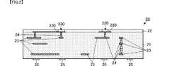
図1に示すように、部品実装基板10は、樹脂基板20、電子部品30、および、モールド樹脂50を備える。 As shown in FIG. 1, the component mounting substrate 10 includes a
樹脂基板20は、図1、図2、図3に示すように、本体樹脂部21と表面樹脂層22とを備える。本体樹脂部21は、複数の樹脂層211,212,213,214,215を備える。複数の樹脂層211,212,213,214,215は、表面側からこの順で積層して配置されている。 As shown in FIGS. 1, 2, and 3, the
複数の樹脂層211,212,213,214,215と表面樹脂層22は、同種の樹脂材料からなる。例えば、複数の樹脂層211,212,213,214,215と表面樹脂層22は、液晶ポリマを主成分としている。液晶ポリマを主成分とすることによって、高周波特性等の電気特性が向上する。The plurality of
複数の樹脂層211,212,213,214,215からなる本体樹脂部21と表面樹脂層22は、一体形成されている。表面樹脂層22は、樹脂層211における樹脂層212と反対側の面に配置されている。言い換えれば、表面樹脂層22は、本体樹脂部21の表面に配置されている。 The main
本体樹脂部21の表面には、ランド導体230が形成されている。ランド導体230は電子部品30を表面実装するための導体であるが、本体樹脂部21の他の回路要素への引き回しのための配線導体も含むものである。本体樹脂部21の裏面には、複数の外部接続用端子導体25が形成されている。本体樹脂部21の内部には、複数の回路導体23および層間接続導体240が形成されている。回路導体23および層間接続導体240は、樹脂基板20で形成する回路構成に準じて形成されている。これら、ランド導体230、回路導体23、層間接続導体240、および、外部接続用端子導体25が、本発明の「樹脂基板に形成された導体パターン」に対応する。
表面樹脂層22には、表面樹脂層22の表面から裏面に貫通する貫通孔220が形成されている。貫通孔220は、表面樹脂層22を本体樹脂部21の表面に配置した状態でランド導体230の一部に重なる位置に形成されている。この構成により、本体樹脂部21の表面に表面樹脂層22が配置された樹脂基板20の表面には、貫通孔220を介して、ランド導体230の一部が露出している。言い換えれば、樹脂基板20の表面には、ランド導体230以外の導体パターンは露出していない。 A through
電子部品30は、本体31および実装用端子32を備える。実装用端子32は、導体からなり、本体31に形成された電子回路に接続されている。実装用端子32は、本体31の裏面に形成されている。 The
電子部品30は、実装用端子32が樹脂基板20側となるように、樹脂基板20の表面に配置されている。この際、実装用端子32は、貫通孔220を介してランド導体230と対向している。この状態において、実装用端子32は、貫通孔220に充填された導電性の接合材40によって、ランド導体230に接合されている。接合材40は、はんだや導電性接着剤等である。 The
モールド樹脂50は、絶縁性を有する。モールド樹脂50は、樹脂基板20を形成する樹脂、すなわち樹脂層211,212,213,214,215、表面樹脂層22を形成する樹脂と異なる材料からなる。モールド樹脂50の樹脂は、樹脂基板20を形成する樹脂に対して高い接合強度が得られる材料からなる。具体的に、樹脂基板20を形成する樹脂が上述の液晶ポリマを主成分とするものである場合、モールド樹脂50は、シリコーンを主成分としている。モールド樹脂50は、さらに絶縁性のフィラー等を含んでいてもよい。 The
モールド樹脂50は、電子部品30が実装された樹脂基板20の表面を覆うように形成されている。この際、モールド樹脂50は、電子部品30も覆うように形成されている。この構成により、電子部品30が実装された樹脂基板20の表面側を、外部環境に対して保護し、部品実装基板10の信頼性を向上することができる。 The
また、本実施形態では、ランド導体230以外の導体パターンが樹脂基板20の表面に露出しておらず、ランド導体230は、接合材40および電子部品30の実装用端子32によって覆われているので、モールド樹脂50は、樹脂基板20の導体パターンには接触していない。これにより、モールド樹脂50が導体パターンに接触することによる導体パターンの導電率の低下が抑制される。したがって、部品実装基板10の電気特性の低下が抑制される。 In the present embodiment, the conductor pattern other than the
このように、本実施形態の構成を用いることによって、信頼性および電気特性に優れた部品実装基板10を実現することができる。 Thus, by using the configuration of the present embodiment, it is possible to realize the component mounting board 10 that is excellent in reliability and electrical characteristics.
また、本実施形態の構成では、表面樹脂層22に形成された貫通孔220によって、樹脂基板20の表面に凹みができ、この凹みに接合材40が形成されている。これにより、接合材40の不要な流れを抑制でき、この接合材40の流れによるリーク等の不具合の発生を抑制することができる。これにより、さらに信頼性の高い部品実装基板10を実現することができる。 In the configuration of the present embodiment, a recess is formed on the surface of the
また、樹脂基板20のヤング率は、モールド樹脂50のヤング率よりも高いことが好ましい。この構成により、外部衝撃から電子部品30を守ることができるようになることに加え、一般的にセラミックやシリコンなど高いヤング率の材料で構成される電子部品30と樹脂基板20のヤング率の差を小さくでき、電子部品30が樹脂基板20から脱落しにくくできるようになる。 The Young's modulus of the
このような構成からなる部品実装基板10は、次に示す工程によって製造されている。 The component mounting board 10 having such a configuration is manufactured by the following process.
まず、複数の樹脂層211,212,213,214,215に導体パターンを形成する。具体的には、片面銅貼りされた樹脂層にパターニング、エッチング処理を施すことによって、回路導体23、ランド導体230、および、外部接続用端子導体25を形成する。また、所定の樹脂層の片面銅貼りされた面とは反対側の面からレーザ等により貫通孔を設け、層間接続導体240の元となる導電ペーストを充填する。また、表面樹脂層22に貫通孔220を形成する。 First, a conductor pattern is formed on the plurality of
表面樹脂層22、および、複数の樹脂層211,212,213,214,215を積層して、加熱圧着する。この加熱圧着により導電ペーストが固化して層間接続導体240が形成される。これにより、表面樹脂層22の貫通孔220によって、表面に凹みを有する樹脂基板20が形成される。この際、樹脂基板20の表面側には、貫通孔220を介したランド導体230の一部以外には、導体が露出していない。 The
樹脂基板20の貫通孔220にはんだペーストを充填する。樹脂基板20の表面に、電子部品30を実装する。この際、電子部品30の実装用端子32が貫通孔220に対向するように、電子部品30を実装する。電子部品30が実装された樹脂基板20を熱処理して、はんだを固化し、電子部品30の実装用端子32と、樹脂基板20のランド導体230を接合する。 A solder paste is filled in the through
電子部品30が接合された樹脂基板20の表面に、モールド樹脂50を充填する。この状態で熱処理を行い、モールド樹脂50を固化する。このような工程を経て、部品実装基板10が形成されている。 A
次に、本発明の第2の実施形態に係る部品実装基板について、図を参照して説明する。図4は、本発明の第2の実施形態に係る部品実装基板の構成を示す側面断面図である。 Next, a component mounting board according to a second embodiment of the present invention will be described with reference to the drawings. FIG. 4 is a side sectional view showing a configuration of a component mounting board according to the second embodiment of the present invention.
本実施形態に係る部品実装基板10Aは、第1の実施形態に係る部品実装基板10に対して、電子部品30Aにおいて異なる。部品実装基板10Aの他の基本構成は、電子部品30Aの形状に応じて樹脂基板20の配線パターンを変更する以外には、第1の実施形態に係る部品実装基板10と同じである。 The
電子部品30Aは、本体31Aおよび実装用端子32Aを備える。実装用端子32Aは、本体31Aの対向する両端に形成されている。実装用端子32Aの一面は、接合材40を介してランド導体230に接合している。この構成においても、ランド導体230は、接合材40および実装用端子32Aによって覆われており、樹脂基板20の表面には導体が露出していない。 The
したがって、本実施形態に係る部品実装基板10Aは、第1の実施形態に係る部品実装基板10と同様の作用効果を得ることができる。 Therefore, the
また、本実施形態の部品実装基板10Aは、電子部品30Aの本体31Aが樹脂基板20の表面に当接している。これにより、上述のはんだの流れをさらに抑制でき、さらに信頼性を向上することができる。なお、このように、電子部品30Aの本体31Aと樹脂基板20の表面を当接させるために、この部分の樹脂基板20の表面を高くする、他の絶縁性部材を介在させる等の構成を用いてもよい。さらには、この電子部品30Aの本体31Aと樹脂基板20を当接させる構成は、第1の実施形態に記載の部品実装基板10の電子部品30と本体31とに適応することもできる。 In the component mounting board 10 </ b> A of the present embodiment, the
次に、本発明の第3の実施形態に係る部品実装基板について、図を参照して説明する。図5は、本発明の第3の実施形態に係る部品実装基板の構成を示す側面断面図である。 Next, a component mounting board according to a third embodiment of the present invention will be described with reference to the drawings. FIG. 5 is a side sectional view showing the configuration of the component mounting board according to the third embodiment of the present invention.
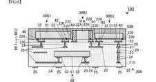
本実施形態に係る部品実装基板10Bは、電子部品30B1,30B2,30B3を実装し、樹脂基板20B内に電子部品60を内蔵した点において、第1、第2の実施形態に係る部品実装基板10,10Aと異なる。本実施形態に係る部品実装基板10Bの他の基本的な構成は、第1、第2の実施形態に係る部品実装基板10,10Aと同じである。 The
電子部品30B1,30B3は、第1の実施形態に係る電子部品30と同じ構造である。電子部品30B2は、第2の実施形態に係る電子部品30Aと同じ構造である。電子部品30B1,30B3の実装用端子32、および、電子部品30B2の実装用端子32Aは、それぞれ、貫通孔220に設けられた接合材40を介して、樹脂基板20Bのランド導体230に接合されている。 The electronic components 30B1 and 30B3 have the same structure as the
電子部品60は、本体61と実装用端子62を備える。実装用端子62は、本体61の裏面に形成されている。電子部品60は、樹脂基板20Bにおける本体樹脂部21Bに内蔵されている。実装用端子62は、層間接続導体24を介して回路導体23に接続されている。 The
樹脂基板20Bの表面には、当該表面の全体および電子部品30B1,30B2,30B3を覆うように、モールド樹脂50Bが形成されている。 A
モールド樹脂50Bは、第1の実施形態に係るモールド樹脂50と同種の材料からなる。モールド樹脂50Bは、樹脂基板20Bを形成する樹脂よりもヤング率が小さい材料からなる。 The
図5に示すように、部品実装基板10Bでは、モールド樹脂50Bと電子部品30B1,30B2,30B3を合わせた体積に対する電子部品30B1,30B2,30B3の体積比率は、樹脂基板20Bに対する電子部品30の体積比率よりも小さい。言い換えれば、モールド樹脂側領域RE2における電子部品の占める体積比率は、樹脂基板側領域RE1における電子部品の占める体積比率よりも小さい。 As shown in FIG. 5, in the
電子部品30B1,30B2,30B3,60は、樹脂基板20Bを形成する樹脂よりもヤング率が大きい。したがって、上述の体積比率の条件で電子部品を配置することによって、モールド樹脂50Bが樹脂基板20Bを形成する樹脂よりもヤング率が小さくても、ヤング率の差によるモールド樹脂50Bと樹脂基板20Bとの界面に生じる応力を抑制することができる。これにより、この界面における破断を抑制でき、さらに信頼性の高い部品実装基板10Bを実現することができる。 The electronic components 30B1, 30B2, 30B3, and 60 have a Young's modulus larger than that of the resin that forms the
また、本実施形態の構成を用いることによって、導体の配線パターンを引き回す領域を樹脂基板20B内に広く設けることができる。これにより、電子部品30B1,30B2,30B3に対する配線用の導体パターンを容易に引き回しでき、導体パターン同士の結合等を抑制できる。これにより、より電気特性に優れる部品実装基板10Bを実現することができる。 Further, by using the configuration of the present embodiment, a region for routing the conductor wiring pattern can be widely provided in the
また、本実施形態の構成を用いることによって、電子部品(内蔵部品)60の起因した樹脂基板20Bの内部応力を小さくできる。一方、電子部品(表面実装部品)30B1,30B2,30B3は、モールド樹脂50B内で内部応力が発生しても、ヤング率の小さい材料からなるモールド樹脂50Bは相対的に変形しやすいため、クラック等が起こりにくくなる。したがって、部品を樹脂基板に実装および内蔵した場合でもクラック等の不具合を抑制できる部品実装基板10Bを得ることができる。 Further, by using the configuration of the present embodiment, the internal stress of the
なお、上述の各実施形態では、樹脂基板に実装される部品として、電子部品を例としているが、電子部品に限るものではなく、実装用端子を備え、樹脂基板に実装されるものであればよい。 In each of the above-described embodiments, an electronic component is taken as an example of the component mounted on the resin substrate. However, the component is not limited to the electronic component, and may be provided with a mounting terminal and mounted on the resin substrate. Good.
10,10A,10B:部品実装基板
20,20B:樹脂基板
21,21B:本体樹脂部
22:表面樹脂層
23:回路導体
24:層間接続導体
25:外部接続用端子導体
30,30A,30B1,30B2,30B3,60:電子部品
31,31A:本体
32,32A:実装用端子
40:接合材
50,50B:モールド樹脂
61:本体
62:実装用端子
211,212,213,214,215:樹脂層
220:貫通孔
230:ランド導体
240:層間接続導体10, 10A, 10B:
Claims (3)
Translated fromJapanese前記樹脂基板の表面に実装され、実装用端子が前記ランド導体に接合される第1の部品と、
前記樹脂基板の表面と前記第1の部品を覆うように形成され、前記樹脂基板とは異なる材質からなるモールド樹脂と、
を備え、
前記樹脂基板は、表面に前記ランド導体が形成された本体樹脂部と、前記本体樹脂部の表面に配置された前記本体樹脂部と同種の材質からなる表面樹脂層とを備え、
前記表面樹脂層の表面には導体が形成されておらず、前記表面樹脂層は、前記ランド導体を前記樹脂基板の表面側に露出させる貫通孔を備え、
前記実装用端子は、前記貫通孔に充填された接合材によって、前記ランド導体に接合されていて、
前記表面樹脂層および前記本体樹脂部は、液晶ポリマを含み、
前記モールド樹脂は、シリコーン樹脂を含む、
部品実装基板。A resin substrate on which a conductor pattern including a land conductor for component mounting is formed;
A first component mounted on the surface of the resin substrate, and a mounting terminal joined to the land conductor;
A mold resin formed so as to cover the surface of the resin substrate and the first component, and made of a material different from the resin substrate;
With
The resin substrate includes a main body resin portion having the land conductor formed on a surface thereof, and a surface resin layer made of the same material as the main body resin portion disposed on the surface of the main body resin portion,
No conductor is formed on the surface of the surface resin layer, and the surface resin layer includes a through hole that exposes the land conductor to the surface side of the resin substrate,
The mounting terminal is bonded to the land conductor by a bonding material filled in the through hole,
The surface resin layer and the main body resin portion include a liquid crystal polymer,
The mold resin includes a silicone resin.
Component mounting board.
前記樹脂基板の表面に実装され、実装用端子が前記ランド導体に接合される第1の部品と、
前記樹脂基板の表面と前記第1の部品を覆うように形成され、前記樹脂基板とは異なる材質からなるモールド樹脂と、
を備え、
前記樹脂基板は、表面に前記ランド導体が形成された本体樹脂部と、前記本体樹脂部の表面に配置された前記本体樹脂部と同種の材質からなる表面樹脂層とを備え、
前記表面樹脂層の表面には導体が形成されておらず、前記表面樹脂層は、前記ランド導体を前記樹脂基板の表面側に露出させる貫通孔を備え、
前記実装用端子は、前記貫通孔に充填された接合材によって、前記ランド導体に接合されていて、
前記樹脂基板のヤング率は、前記モールド樹脂のヤング率よりも高い、
部品実装基板。A resin substrate on which a conductor pattern including a land conductor for component mounting is formed;
A first component mounted on the surface of the resin substrate, and a mounting terminal joined to the land conductor;
A mold resin formed so as to cover the surface of the resin substrate and the first component, and made of a material different from the resin substrate;
With
The resin substrate includes a main body resin portion having the land conductor formed on a surface thereof, and a surface resin layer made of the same material as the main body resin portion disposed on the surface of the main body resin portion,
No conductor is formed on the surface of the surface resin layer, and the surface resin layer includes a through hole that exposes the land conductor to the surface side of the resin substrate,
The mounting terminal is bonded to the land conductor by a bonding material filled in the through hole,
The Young's modulus of the resin substrate is higher than the Young's modulus of the mold resin.
Component mounting board.
前記樹脂基板の表面に実装され、実装用端子が前記ランド導体に接合される第1の部品と、
前記樹脂基板の表面と前記第1の部品を覆うように形成され、前記樹脂基板とは異なる材質からなるモールド樹脂と、
を備え、
前記樹脂基板は、表面に前記ランド導体が形成された本体樹脂部と、前記本体樹脂部の表面に配置された前記本体樹脂部と同種の材質からなる表面樹脂層とを備え、
前記表面樹脂層の表面には導体が形成されておらず、前記表面樹脂層は、前記ランド導体を前記樹脂基板の表面側に露出させる貫通孔を備え、
前記実装用端子は、前記貫通孔に充填された接合材によって、前記ランド導体に接合されていて、
前記本体樹脂部に内蔵された第2の部品を備え、
前記モールド樹脂は、前記表面樹脂層および前記本体樹脂部よりもヤング率の小さい材料からなり、
前記第2の部品を含む前記樹脂基板の体積に対する前記第2の部品の体積の比率は、前記モールド樹脂と前記第1の部品とからなる体積に対する前記第1の部品の体積の比率よりも小さい、
部品実装基板。A resin substrate on which a conductor pattern including a land conductor for component mounting is formed;
A first component mounted on the surface of the resin substrate, and a mounting terminal joined to the land conductor;
A mold resin formed so as to cover the surface of the resin substrate and the first component, and made of a material different from the resin substrate;
With
The resin substrate includes a main body resin portion having the land conductor formed on a surface thereof, and a surface resin layer made of the same material as the main body resin portion disposed on the surface of the main body resin portion,
No conductor is formed on the surface of the surface resin layer, and the surface resin layer includes a through hole that exposes the land conductor to the surface side of the resin substrate,
The mounting terminal is bonded to the land conductor by a bonding material filled in the through hole,
A second component built in the main body resin portion;
The mold resin is made of a material having a smaller Young's modulus than the surface resin layer and the main body resin portion,
The ratio of the volume of the second component to the volume of the resin substrate including the second component is smaller than the ratio of the volume of the first component to the volume composed of the mold resin and the first component. ,
Component mounting board.
Applications Claiming Priority (3)
| Application Number | Priority Date | Filing Date | Title |
|---|---|---|---|
| JP2015217374 | 2015-11-05 | ||
| JP2015217374 | 2015-11-05 | ||
| PCT/JP2016/080465WO2017077837A1 (en) | 2015-11-05 | 2016-10-14 | Component-mounted substrate |
Publications (2)
| Publication Number | Publication Date |
|---|---|
| JP6323622B2true JP6323622B2 (en) | 2018-05-16 |
| JPWO2017077837A1 JPWO2017077837A1 (en) | 2018-06-14 |
Family
ID=58661961
Family Applications (1)
| Application Number | Title | Priority Date | Filing Date |
|---|---|---|---|
| JP2017548693AActiveJP6323622B2 (en) | 2015-11-05 | 2016-10-14 | Component mounting board |
Country Status (4)
| Country | Link |
|---|---|
| US (1) | US10154597B2 (en) |
| JP (1) | JP6323622B2 (en) |
| CN (1) | CN208159004U (en) |
| WO (1) | WO2017077837A1 (en) |
Families Citing this family (2)
| Publication number | Priority date | Publication date | Assignee | Title |
|---|---|---|---|---|
| WO2018123382A1 (en)* | 2016-12-28 | 2018-07-05 | 株式会社村田製作所 | Circuit module |
| JP7407732B2 (en)* | 2018-12-04 | 2024-01-04 | 株式会社クラレ | High voltage circuit board and high voltage device using the same |
Family Cites Families (15)
| Publication number | Priority date | Publication date | Assignee | Title |
|---|---|---|---|---|
| US5490324A (en)* | 1993-09-15 | 1996-02-13 | Lsi Logic Corporation | Method of making integrated circuit package having multiple bonding tiers |
| TW411537B (en)* | 1998-07-31 | 2000-11-11 | Siliconware Precision Industries Co Ltd | Semiconductor package with CSP-BGA structure |
| US6861588B2 (en)* | 2002-07-16 | 2005-03-01 | Murata Manufacturing Co., Ltd. | Laminated ceramic electronic component and method of producing the same |
| JP4357817B2 (en)* | 2002-09-12 | 2009-11-04 | パナソニック株式会社 | Module with built-in circuit components |
| US6998532B2 (en)* | 2002-12-24 | 2006-02-14 | Matsushita Electric Industrial Co., Ltd. | Electronic component-built-in module |
| DE10300956B3 (en)* | 2003-01-13 | 2004-07-15 | Epcos Ag | Device with high frequency connections in a substrate |
| JP2005108950A (en)* | 2003-09-29 | 2005-04-21 | Matsushita Electric Ind Co Ltd | Ceramic module component and manufacturing method thereof |
| JP2005136043A (en)* | 2003-10-29 | 2005-05-26 | Kyocera Corp | Wiring board and electrical device |
| JP5262530B2 (en)* | 2008-09-30 | 2013-08-14 | セイコーエプソン株式会社 | Electronic device and method for manufacturing electronic device |
| CN103460821B (en) | 2011-04-01 | 2016-08-10 | 株式会社村田制作所 | Component built-in resin substrate and manufacturing method thereof |
| WO2014024754A1 (en)* | 2012-08-07 | 2014-02-13 | 三菱瓦斯化学株式会社 | Circuit board for semiconductor package and method for producing same |
| JP5285819B1 (en)* | 2012-11-07 | 2013-09-11 | 太陽誘電株式会社 | Electronic circuit module |
| JP5958558B2 (en) | 2012-12-18 | 2016-08-02 | 株式会社村田製作所 | Resin multilayer board |
| US10269688B2 (en)* | 2013-03-14 | 2019-04-23 | General Electric Company | Power overlay structure and method of making same |
| US8987876B2 (en) | 2013-03-14 | 2015-03-24 | General Electric Company | Power overlay structure and method of making same |
- 2016
- 2016-10-14JPJP2017548693Apatent/JP6323622B2/enactiveActive
- 2016-10-14CNCN201690001288.7Upatent/CN208159004U/enactiveActive
- 2016-10-14WOPCT/JP2016/080465patent/WO2017077837A1/ennot_activeCeased
- 2018
- 2018-04-19USUS15/956,787patent/US10154597B2/enactiveActive
Also Published As
| Publication number | Publication date |
|---|---|
| US10154597B2 (en) | 2018-12-11 |
| CN208159004U (en) | 2018-11-27 |
| US20180242459A1 (en) | 2018-08-23 |
| JPWO2017077837A1 (en) | 2018-06-14 |
| WO2017077837A1 (en) | 2017-05-11 |
Similar Documents
| Publication | Publication Date | Title |
|---|---|---|
| US9947466B2 (en) | Electronic component | |
| US9082550B2 (en) | Electronic component | |
| JP6891965B2 (en) | High frequency module and its manufacturing method | |
| JP5756500B2 (en) | Circuit module | |
| US10014111B2 (en) | Substrate terminal mounted electronic element | |
| US20080272469A1 (en) | Semiconductor die package and integrated circuit package and fabricating method thereof | |
| JP5628772B2 (en) | Printed circuit board and electronic device using the same | |
| JPWO2015060387A1 (en) | Wiring board and electronic device | |
| JP6323622B2 (en) | Component mounting board | |
| JP2005197354A (en) | Semiconductor module and manufacturing method thereof | |
| JP5201271B2 (en) | Circuit board and manufacturing method thereof | |
| WO2012172890A1 (en) | Printed-wiring board, electronic-component mounting structure, and method for manufacturing electronic-component mounting structure | |
| JP2008034672A (en) | Method for mounting chip component, and electronic module | |
| JPWO2009090896A1 (en) | Electronic components | |
| JP6477894B2 (en) | Resin circuit board, component-mounted resin circuit board | |
| JP6191808B1 (en) | Multilayer substrate and electronic equipment | |
| JP2008159731A (en) | Electronic component mounting board | |
| JP4353131B2 (en) | Electronic equipment | |
| KR100847647B1 (en) | Printed circuit board | |
| JP2006286660A (en) | Three-dimensional electronic circuit device | |
| JP2006066665A (en) | Wiring board | |
| JP2017204490A (en) | Component mounting board, manufacturing method of component mounting board | |
| JP2015065207A (en) | Ceramic substrate end face electrode for surface-mounted electronic component | |
| JP2013098364A (en) | Module component and wiring board for use in the same | |
| JP2009272510A (en) | Mounting structure for ic package, method for manufacturing the same and its sheet capacitor |
Legal Events
| Date | Code | Title | Description |
|---|---|---|---|
| A521 | Request for written amendment filed | Free format text:JAPANESE INTERMEDIATE CODE: A523 Effective date:20180214 | |
| A621 | Written request for application examination | Free format text:JAPANESE INTERMEDIATE CODE: A621 Effective date:20180214 | |
| A871 | Explanation of circumstances concerning accelerated examination | Free format text:JAPANESE INTERMEDIATE CODE: A871 Effective date:20180214 | |
| A975 | Report on accelerated examination | Free format text:JAPANESE INTERMEDIATE CODE: A971005 Effective date:20180302 | |
| TRDD | Decision of grant or rejection written | ||
| A01 | Written decision to grant a patent or to grant a registration (utility model) | Free format text:JAPANESE INTERMEDIATE CODE: A01 Effective date:20180313 | |
| A61 | First payment of annual fees (during grant procedure) | Free format text:JAPANESE INTERMEDIATE CODE: A61 Effective date:20180326 | |
| R150 | Certificate of patent or registration of utility model | Ref document number:6323622 Country of ref document:JP Free format text:JAPANESE INTERMEDIATE CODE: R150 |