JP6322380B2 - Display device - Google Patents
Display deviceDownload PDFInfo
- Publication number
- JP6322380B2 JP6322380B2JP2013216298AJP2013216298AJP6322380B2JP 6322380 B2JP6322380 B2JP 6322380B2JP 2013216298 AJP2013216298 AJP 2013216298AJP 2013216298 AJP2013216298 AJP 2013216298AJP 6322380 B2JP6322380 B2JP 6322380B2
- Authority
- JP
- Japan
- Prior art keywords
- layer
- silicon oxide
- resin layer
- oxide film
- film
- Prior art date
- Legal status (The legal status is an assumption and is not a legal conclusion. Google has not performed a legal analysis and makes no representation as to the accuracy of the status listed.)
- Active
Links
Images


Classifications
- H—ELECTRICITY
- H10—SEMICONDUCTOR DEVICES; ELECTRIC SOLID-STATE DEVICES NOT OTHERWISE PROVIDED FOR
- H10D—INORGANIC ELECTRIC SEMICONDUCTOR DEVICES
- H10D86/00—Integrated devices formed in or on insulating or conducting substrates, e.g. formed in silicon-on-insulator [SOI] substrates or on stainless steel or glass substrates
- H10D86/01—Manufacture or treatment
- H10D86/021—Manufacture or treatment of multiple TFTs
- H10D86/0214—Manufacture or treatment of multiple TFTs using temporary substrates
- H—ELECTRICITY
- H10—SEMICONDUCTOR DEVICES; ELECTRIC SOLID-STATE DEVICES NOT OTHERWISE PROVIDED FOR
- H10D—INORGANIC ELECTRIC SEMICONDUCTOR DEVICES
- H10D30/00—Field-effect transistors [FET]
- H10D30/01—Manufacture or treatment
- H10D30/021—Manufacture or treatment of FETs having insulated gates [IGFET]
- H10D30/031—Manufacture or treatment of FETs having insulated gates [IGFET] of thin-film transistors [TFT]
- H10D30/0312—Manufacture or treatment of FETs having insulated gates [IGFET] of thin-film transistors [TFT] characterised by the gate electrodes
- H10D30/0314—Manufacture or treatment of FETs having insulated gates [IGFET] of thin-film transistors [TFT] characterised by the gate electrodes of lateral top-gate TFTs comprising only a single gate
- H—ELECTRICITY
- H10—SEMICONDUCTOR DEVICES; ELECTRIC SOLID-STATE DEVICES NOT OTHERWISE PROVIDED FOR
- H10D—INORGANIC ELECTRIC SEMICONDUCTOR DEVICES
- H10D30/00—Field-effect transistors [FET]
- H10D30/01—Manufacture or treatment
- H10D30/021—Manufacture or treatment of FETs having insulated gates [IGFET]
- H10D30/031—Manufacture or treatment of FETs having insulated gates [IGFET] of thin-film transistors [TFT]
- H10D30/0321—Manufacture or treatment of FETs having insulated gates [IGFET] of thin-film transistors [TFT] comprising silicon, e.g. amorphous silicon or polysilicon
- H—ELECTRICITY
- H10—SEMICONDUCTOR DEVICES; ELECTRIC SOLID-STATE DEVICES NOT OTHERWISE PROVIDED FOR
- H10D—INORGANIC ELECTRIC SEMICONDUCTOR DEVICES
- H10D30/00—Field-effect transistors [FET]
- H10D30/60—Insulated-gate field-effect transistors [IGFET]
- H10D30/67—Thin-film transistors [TFT]
- H10D30/674—Thin-film transistors [TFT] characterised by the active materials
- H10D30/6741—Group IV materials, e.g. germanium or silicon carbide
- H—ELECTRICITY
- H10—SEMICONDUCTOR DEVICES; ELECTRIC SOLID-STATE DEVICES NOT OTHERWISE PROVIDED FOR
- H10D—INORGANIC ELECTRIC SEMICONDUCTOR DEVICES
- H10D62/00—Semiconductor bodies, or regions thereof, of devices having potential barriers
- H10D62/40—Crystalline structures
- H—ELECTRICITY
- H10—SEMICONDUCTOR DEVICES; ELECTRIC SOLID-STATE DEVICES NOT OTHERWISE PROVIDED FOR
- H10D—INORGANIC ELECTRIC SEMICONDUCTOR DEVICES
- H10D62/00—Semiconductor bodies, or regions thereof, of devices having potential barriers
- H10D62/80—Semiconductor bodies, or regions thereof, of devices having potential barriers characterised by the materials
- H10D62/83—Semiconductor bodies, or regions thereof, of devices having potential barriers characterised by the materials being Group IV materials, e.g. B-doped Si or undoped Ge
- H—ELECTRICITY
- H10—SEMICONDUCTOR DEVICES; ELECTRIC SOLID-STATE DEVICES NOT OTHERWISE PROVIDED FOR
- H10D—INORGANIC ELECTRIC SEMICONDUCTOR DEVICES
- H10D86/00—Integrated devices formed in or on insulating or conducting substrates, e.g. formed in silicon-on-insulator [SOI] substrates or on stainless steel or glass substrates
- H10D86/40—Integrated devices formed in or on insulating or conducting substrates, e.g. formed in silicon-on-insulator [SOI] substrates or on stainless steel or glass substrates characterised by multiple TFTs
- H10D86/411—Integrated devices formed in or on insulating or conducting substrates, e.g. formed in silicon-on-insulator [SOI] substrates or on stainless steel or glass substrates characterised by multiple TFTs characterised by materials, geometry or structure of the substrates
- H—ELECTRICITY
- H10—SEMICONDUCTOR DEVICES; ELECTRIC SOLID-STATE DEVICES NOT OTHERWISE PROVIDED FOR
- H10D—INORGANIC ELECTRIC SEMICONDUCTOR DEVICES
- H10D86/00—Integrated devices formed in or on insulating or conducting substrates, e.g. formed in silicon-on-insulator [SOI] substrates or on stainless steel or glass substrates
- H10D86/40—Integrated devices formed in or on insulating or conducting substrates, e.g. formed in silicon-on-insulator [SOI] substrates or on stainless steel or glass substrates characterised by multiple TFTs
- H10D86/421—Integrated devices formed in or on insulating or conducting substrates, e.g. formed in silicon-on-insulator [SOI] substrates or on stainless steel or glass substrates characterised by multiple TFTs having a particular composition, shape or crystalline structure of the active layer
- H—ELECTRICITY
- H10—SEMICONDUCTOR DEVICES; ELECTRIC SOLID-STATE DEVICES NOT OTHERWISE PROVIDED FOR
- H10D—INORGANIC ELECTRIC SEMICONDUCTOR DEVICES
- H10D86/00—Integrated devices formed in or on insulating or conducting substrates, e.g. formed in silicon-on-insulator [SOI] substrates or on stainless steel or glass substrates
- H10D86/40—Integrated devices formed in or on insulating or conducting substrates, e.g. formed in silicon-on-insulator [SOI] substrates or on stainless steel or glass substrates characterised by multiple TFTs
- H10D86/60—Integrated devices formed in or on insulating or conducting substrates, e.g. formed in silicon-on-insulator [SOI] substrates or on stainless steel or glass substrates characterised by multiple TFTs wherein the TFTs are in active matrices
Landscapes
- Electroluminescent Light Sources (AREA)
- Chemical & Material Sciences (AREA)
- Crystallography & Structural Chemistry (AREA)
- Devices For Indicating Variable Information By Combining Individual Elements (AREA)
- Thin Film Transistor (AREA)
- Recrystallisation Techniques (AREA)
Description
Translated fromJapanese本発明の実施形態は、表示装置に関する。 Embodiments described herein relate generally to a display device.
有機エレクトロルミネッセンス(EL)表示装置や液晶表示装置などの平面表示装置は、軽量、薄型、低消費電力などの特長を生かして、OA(office automation)機器、情報端末、時計、テレビ受像機などの各種分野で利用されている。中でも薄膜トランジスタ(TFT)を用いた表示装置は、その応答性の高さから携帯端末やコンピュータなど多くの情報を表示するモニタとして多用されている。 Flat display devices such as organic electroluminescence (EL) display devices and liquid crystal display devices are OA (office automation) devices, information terminals, watches, television receivers, etc., taking advantage of their light weight, thinness, and low power consumption. Used in various fields. In particular, a display device using a thin film transistor (TFT) is widely used as a monitor for displaying a large amount of information such as a portable terminal and a computer because of its high responsiveness.
近年、携帯電話やPDA(personal digital assistant)などの携帯情報端末機器では性能面もさることながら、デザイン性、携帯性などの観点から、より薄く、しかもより軽い表示装置の要求が高まっている。例えば、より一層の薄型化構造を実現とする表示装置が提案されている。薄型化及び軽量化を実現する方法として、ガラス基板に替えて比較的耐熱性が高いポリイミドからなる樹脂層やプラスチック基板を利用する技術が知られている。ポリイミドで樹脂層を形成する際は、ポリイミドを利用した樹脂層をガラス基板上に形成し、樹脂層上にTFTなどを形成した後にセル化を行い、最終的にガラス基板から樹脂層を剥離する。これにより、上記樹脂層を形成することができる。 In recent years, portable information terminal devices such as mobile phones and PDAs (personal digital assistants) are demanding thinner and lighter display devices from the viewpoints of design and portability, as well as performance. For example, a display device that realizes a thinner structure has been proposed. As a method for realizing a reduction in thickness and weight, a technique using a resin layer or a plastic substrate made of polyimide having relatively high heat resistance instead of a glass substrate is known. When forming a resin layer with polyimide, a resin layer using polyimide is formed on a glass substrate, and after forming a TFT or the like on the resin layer, a cell is formed, and finally the resin layer is peeled from the glass substrate. . Thereby, the resin layer can be formed.
本発明の実施形態の目的は、可撓性及び製品信頼性に優れた表示装置を提供することにある。 An object of an embodiment of the present invention is to provide a display device having excellent flexibility and product reliability.
一実施形態に係る表示装置は、
樹脂層表面上に形成された下地絶縁層と、
前記下地絶縁層を介して前記樹脂層表面の上方に形成された薄膜トランジスタの活性層と、を備え、
前記下地絶縁層は、第1シリコン酸化膜と、前記第1シリコン酸化膜の上方に形成されたシリコン窒化膜と、前記シリコン窒化膜の上方に形成された第2シリコン酸化膜の3層積層構造を含み、
前記下地絶縁層において、前記樹脂層に接する層は前記第1シリコン酸化膜であり、
前記第1シリコン酸化膜は、前記樹脂層の周縁部まで形成され、
前記樹脂層の下面を除いた上面と周縁面は前記第1シリコン酸化膜で覆われている。
A display device according to an embodiment includes:
A base insulating layer formed on the surface of the resin layer;
An active layer of a thin film transistor formed above the surface of the resin layer through the base insulating layer,
The base insulating layer has a three-layer structure of a first silicon oxide film, a silicon nitride film formed above the first silicon oxide film, and a second silicon oxide film formed above the silicon nitride film. Including
In the base insulating layer, the layer in contact with the resin layer is the first silicon oxide film,
The first silicon oxide film is formed upto a peripheral edge of the resin layer,
The upper surface and the peripheral surface excluding the lower surface of the resin layer are covered with the first silicon oxide film.
始めに、本発明の実施形態の着想について説明する。
表示装置は、ガラス基板又は樹脂層の上方にTFT(薄膜トランジスタ)を形成する等して形成される。ガラス基板又は樹脂層と、TFTとの間にはアンダーコート層が設けられている。アンダーコート層は、TFTの汚染(ガラス基板又は樹脂層からTFTへの不純物の拡散)を防止するためである。また、アンダーコート層は、下地絶縁層であり、TFTと電気的に隔離されている。First, the idea of the embodiment of the present invention will be described.
The display device is formed by forming a TFT (thin film transistor) on a glass substrate or a resin layer. An undercoat layer is provided between the glass substrate or the resin layer and the TFT. The undercoat layer is for preventing contamination of the TFT (diffusion of impurities from the glass substrate or the resin layer to the TFT). The undercoat layer is a base insulating layer and is electrically isolated from the TFT.
例えば、ガラス基板を利用して表示装置を形成し、Si(シリコン)を利用してTFTを形成する場合、例えばアンダーコート層はガラス基板上に形成され、TFTはアンダーコート層を介してガラス基板上に形成される。アンダーコート層は、2層積層構造を含み、SiNX膜(シリコン窒化膜)と、SiO2膜(シリコン酸化膜)とを有している。SiNX膜はガラス基板上に形成され、SiO2膜はSiNX膜上に形成されている。SiNX及びSiO2は無機材料であるため、例えばSiNX膜及びSiO2膜はプラズマCVD(chemical vapor deposition)法を利用して形成される。For example, when a display device is formed using a glass substrate and a TFT is formed using Si (silicon), for example, the undercoat layer is formed on the glass substrate, and the TFT is formed on the glass substrate via the undercoat layer. Formed on top. The undercoat layer includes a two-layer laminated structure, and includes a SiNX film (silicon nitride film) and a SiO2 film (silicon oxide film). The SiNX film is formed on the glass substrate, and the SiO2 film is formed on the SiNX film. Since SiNX and SiO2 are inorganic materials, for example, the SiNX film and the SiO2 film are formed using a plasma CVD (chemical vapor deposition) method.
ここで、SiNX膜の特長と、難点を示す。
特長:イオンブロッキング性に優れているためTFTの汚染を防止することができる。
難点:SiNX膜の直上にSi層が形成されている場合、TFTの電気的特性に悪影響が及び、TFTのスイッチング素子としての使用が困難となる場合がある。Si層を多結晶化する際、SiNX膜の構成要素の窒素原子(余剰窒素)がSi層中に供給されるためである。上記のことは、N型ドーパントと同じ働きがあるため、Si層に電子を排出する機能を不所望に持たせてしまう。言い換えると、Si層の中で、窒素原子がドナーとして働いてしまい、電流を流したくないとき、電流を流し易くなってしまう。さらに言い換えると、Si層のチャネル領域を高抵抗にしなければならない状況においても、チャネル領域を流れるリーク電流が増大してしまう。Here, the features and difficulties of the SiNX film are shown.
Features: Because of its excellent ion blocking property, it can prevent TFT contamination.
Difficulties: When the Si layer is formed directly on the SiNX film, the electrical characteristics of the TFT are adversely affected, and it may be difficult to use the TFT as a switching element. This is because when the Si layer is polycrystallized, nitrogen atoms (surplus nitrogen) as a constituent element of the SiNX film are supplied into the Si layer. Since the above has the same function as the N-type dopant, the Si layer is undesirably given the function of discharging electrons. In other words, in the Si layer, nitrogen atoms work as donors, and when it is not desired to flow current, it becomes easy to flow current. In other words, even in a situation where the channel region of the Si layer must have a high resistance, the leakage current flowing through the channel region increases.
続いて、SiO2膜の特長と、難点を示す。
特長1:Si層との親和性に優れている。
特長2:不純物ドーピングの際の影響が小さい。
特長3:SiNX膜からSi層中への窒素原子(余剰窒素)の供給を防止することができる。
難点:TFTの汚染の防止への寄与が乏しい。Next, features and difficulties of the SiO2 film will be described.
Feature 1: Excellent affinity with Si layer.
Feature 2: Impact during impurity doping is small.
Feature 3: Supply of nitrogen atoms (surplus nitrogen) from the SiNX film into the Si layer can be prevented.
Difficulties: poor contribution to prevention of TFT contamination.
次いで、ガラス基板上に、アンダーコート層と、p−Si(ポリシリコン)を利用したTFTとを形成するための製造方法について説明する。
この場合、アンダーコート層と、a−Si(アモルファスシリコン)層とは同一機会にされることが多い。例えば、ガラス基板の温度が400℃程度となる同一CVD反応室内で、供給ガスの切替えのみで、ガラス基板上に、SiNX膜、SiO2膜、及びa−Si層の3層が連続的に順に形成される。SiNX膜は、SiH4ガスとNH3ガスとの混合ガスのプラズマ分解によりガラス基板上に形成される。SiO2膜は、SiH4ガスとN2Oガスとの混合ガスのプラズマ分解によりSiNX膜上に形成される。a−Si層は、SiH4ガスのプラズマ分解によりSiO2膜上に形成される。以降は、通常の低温p−Siを利用するTFTの製造工程を経る。Next, a manufacturing method for forming an undercoat layer and a TFT using p-Si (polysilicon) on a glass substrate will be described.
In this case, the undercoat layer and the a-Si (amorphous silicon) layer are often used on the same occasion. For example, three layers of a SiNX film, a SiO2 film, and an a-Si layer are continuously formed on the glass substrate only by switching the supply gas in the same CVD reaction chamber where the temperature of the glass substrate is about 400 ° C. It is formed in order. The SiNX film is formed on the glass substrate by plasma decomposition of a mixed gas of SiH4 gas and NH3 gas. The SiO2 film is formed on the SiNX film by plasma decomposition of a mixed gas of SiH4 gas and N2 O gas. The a-Si layer is formed on the SiO2 film by plasma decomposition of SiH4 gas. Thereafter, a TFT manufacturing process using normal low-temperature p-Si is performed.
上記のように、ガラス基板上方にTFTを形成する場合、SiNX膜及びSiO2膜の2層でアンダーコート層を形成することにより、製品信頼性に優れた表示装置を得ることができる。As described above, when the TFT is formed above the glass substrate, a display device having excellent product reliability can be obtained by forming the undercoat layer with two layers of the SiNX film and the SiO2 film.
ところで、表示装置のうち、ガラス基板の替わりとして、可撓性に優れた材料で形成された基板を備えた表示装置の開発が進められている。製品信頼性に優れ、かつ可撓性に優れた(割れ難い)表示装置を得たいためである。その他にも、ガラス基板を備えた表示装置と異なり、商品のデザインを制約しない等の利点があるためである。 By the way, development of the display apparatus provided with the board | substrate formed with the material excellent in flexibility instead of a glass substrate among display apparatuses is advanced. This is because it is desired to obtain a display device having excellent product reliability and flexibility (hard to break). In addition, unlike a display device provided with a glass substrate, there is an advantage that the design of the product is not restricted.
可撓性に優れた基板の作製方法としては、次に挙げる、概ね2種類がある。
(1)ガラス基板の替わりに、プラスチック基板(樹脂基板)を用いる。As a method for manufacturing a substrate having excellent flexibility, there are roughly two types as follows.
(1) A plastic substrate (resin substrate) is used instead of the glass substrate.
(2)ガラス基板上に樹脂層(例えば、ポリイミドを利用した樹脂層)を形成し、ガラス基板から樹脂層を剥離する。これにより、上記樹脂層をガラス基板の替わりに用いる。 (2) A resin layer (for example, a resin layer using polyimide) is formed on a glass substrate, and the resin layer is peeled from the glass substrate. Thereby, the said resin layer is used instead of a glass substrate.
また、プラスチック基板や樹脂層を利用して表示装置を形成する場合も、TFTの汚染を防止するため、アンダーコート層はプラスチック基板や樹脂層上に形成される。TFTは、アンダーコート層を介してプラスチック基板や樹脂層の上方に形成される。また、この場合、SiNX膜及びSiO2膜の2層でアンダーコート層を形成することが考えられる。SiNX膜は、樹脂層表面(プラスチック基板表面又は樹脂層表面)上に形成され、SiO2膜は、SiNX膜上に形成される。Further, when a display device is formed using a plastic substrate or a resin layer, the undercoat layer is formed on the plastic substrate or the resin layer in order to prevent TFT contamination. The TFT is formed above the plastic substrate and the resin layer via the undercoat layer. In this case, it is conceivable to form an undercoat layer with two layers of a SiNX film and a SiO2 film. The SiNX film is formed on the resin layer surface (plastic substrate surface or resin layer surface), and the SiO2 film is formed on the SiNX film.
しかしながら、上記のように樹脂層表面上にSiNX膜を形成した場合、樹脂層(特に、樹脂層表面)が変質してしまうという課題が生じる。ここで、上記変質とは、樹脂層が硬化し、樹脂層の可撓性(軟らかさ)が失われることをいう。樹脂層が変質すると、樹脂層が脆くなり、割れ(脆性破壊)が生じ易くなる。このため、ガラスを樹脂に替えて表示装置を形成しても、可撓性に優れた表示装置を得ることは困難となる。However, when the SiNX film is formed on the surface of the resin layer as described above, there arises a problem that the resin layer (particularly the surface of the resin layer) is altered. Here, the above-mentioned alteration means that the resin layer is cured and the flexibility (softness) of the resin layer is lost. When the resin layer is altered, the resin layer becomes brittle and cracks (brittle fracture) are likely to occur. For this reason, even if it replaces glass with resin and forms a display device, it becomes difficult to obtain a display device excellent in flexibility.
なぜなら、SiNX膜を形成する際、400℃程度の高温となった樹脂層表面が還元性の高いNH3ガスに曝されるためである。なお、NH3ガスを用いること無しにSiNX膜を形成しても、樹脂層(樹脂層表面)に変質が生じる結果となった。例えば、SiH4ガスとN2ガスとの混合ガスのプラズマ分解によりSiNX膜を形成しても、樹脂層(樹脂層表面)に変質が生じてしまう。その他にも、SiH4ガスのみのプラズマ分解によりa−Si膜を形成しても、樹脂層(樹脂層表面)に変質が生じてしまう。上記のことから、樹脂層(樹脂層表面)が還元性の雰囲気に曝されると、樹脂層(樹脂層表面)に変質が生じることが分かった。This is because when the SiNX film is formed, the surface of the resin layer having a high temperature of about 400 ° C. is exposed to highly reducible NH3 gas. Even if the SiNX film was formed without using NH3 gas, the resin layer (resin layer surface) was altered. For example, even if the SiNX film is formed by plasma decomposition of a mixed gas of SiH4 gas and N2 gas, the resin layer (resin layer surface) is altered. In addition, even if an a-Si film is formed by plasma decomposition of only SiH4 gas, the resin layer (resin layer surface) is altered. From the above, it was found that when the resin layer (resin layer surface) is exposed to a reducing atmosphere, the resin layer (resin layer surface) is altered.
上述したことから分かるように、上述したようなアンダーコート層(下地絶縁層)の形成手法では、可撓性に優れた表示装置を得ることは困難である。
そこで、本発明の実施形態においては、この課題の原因を解明し、この課題を解決することにより、可撓性及び製品信頼性に優れた表示装置を得ることができるものである。次に、本発明の実施形態の課題解決のため、上記着想を具体化する手段について説明する。As can be seen from the above, it is difficult to obtain a display device with excellent flexibility by the above-described method for forming an undercoat layer (underlying insulating layer).
Therefore, in the embodiment of the present invention, by elucidating the cause of this problem and solving this problem, a display device having excellent flexibility and product reliability can be obtained. Next, in order to solve the problem of the embodiment of the present invention, means for realizing the above idea will be described.
以下、図面を参照しながら第1の実施形態に係る表示装置について詳細に説明する。本実施形態では、シート状の表示装置の一例として、有機EL表示装置について説明する。 Hereinafter, the display device according to the first embodiment will be described in detail with reference to the drawings. In the present embodiment, an organic EL display device will be described as an example of a sheet-like display device.
図1に示すように、有機EL表示装置DAは、アクティブマトリクス駆動方式を採用したものであり、アレイ基板ARと、対向基板CTとを備えている。アレイ基板ARは、樹脂層10を用いて形成されている。アレイ基板ARは、樹脂層10の内面10A側に、スイッチング素子SW1乃至SW3、有機EL素子OLED1乃至OLED3などを備えている。 As shown in FIG. 1, the organic EL display device DA employs an active matrix driving method, and includes an array substrate AR and a counter substrate CT. The array substrate AR is formed using the
樹脂層10は、絶縁層であり、例えば、ポリイミド(PI)を主成分とする材料によって形成されている。この樹脂層10は、例えば、5乃至30μmの厚さを有している。樹脂層10を形成する材料としては、ポリイミドの他、ポリアミドイミド、ポリアラミド等、耐熱性に富む材料を用いることが好ましい。 The
樹脂層10の内面10Aは、第1絶縁膜としての下地絶縁層11によって覆われている。すなわち、下地絶縁層11は、アンダーコート層であり、樹脂層10の表面上に形成されている。下地絶縁層11は、樹脂層10からのイオン性の不純物の浸入や、樹脂層10を介した水分などの浸入を抑制する内面バリア膜として機能する。このような下地絶縁層11は、無機系材料によって形成され、例えばSiNX膜(シリコン窒化膜)とSiO2膜(シリコン酸化膜)との積層体によって形成されている。下地絶縁層11は、SiON膜(シリコン酸窒化膜)をさらに有して形成されていてもよい。なお、下地絶縁層11の詳細な説明については後述する。The
スイッチング素子SW1乃至SW3は、下地絶縁層11の上に形成されている。すなわち、スイッチング素子SW1乃至SW3は、下地絶縁層11を介して樹脂層表面の上方に形成されている。これらのスイッチング素子SW1乃至SW3は、それぞれ活性層としての半導体層SCを備えたTFT(薄膜トランジスタ)である。半導体層SCの厚みは、例えば50nmである。スイッチング素子SW1乃至SW3は、いずれも同一構造であるが、ここでは、スイッチング素子SW1に着目してその構造をより具体的に説明する。 The switching elements SW1 to SW3 are formed on the
スイッチング素子SW1は、トップゲート型であるが、これは一例であり、ボトムゲート型での構成を妨げるものではない。ただし、トップゲート型においては、半導体層、とくにチャネル領域となる部分が下地絶縁膜11と直接接することから、本実施形態で示す下地絶縁層11の構成がより好適となる。この実施形態において、半導体層SCはp−Siで形成されている。但し、半導体層SCは、p−Si以外の材料で形成することができ、a−Siや、インジウム(In)、ガリウム(Ga)、亜鉛(Zn)の少なくとも1つを含む酸化物によって形成された酸化物半導体で形成されていてもよい。酸化物半導体は、a−Siやp−Siよりも低温プロセスでの形成が可能である。特に、IGZOなどの酸化物半導体は、a−Si半導体層を具備するTFTを製造してきた製造装置をそのまま使用することも可能となるため、製造設備の投資コストを押える点でも好ましい。 Although the switching element SW1 is a top gate type, this is an example and does not disturb the configuration of the bottom gate type. However, in the top gate type, the structure of the
半導体層SCは、下地絶縁層11の上に形成され、第2絶縁膜12によって覆われている。第2絶縁膜12は、ゲート絶縁膜であり、下地絶縁層11の上にも配置されている。第2絶縁膜12の上には、スイッチング素子SW1のゲート電極WGが形成されている。ゲート電極WGは、第3絶縁膜13によって覆われている。第3絶縁膜13は、第2絶縁膜12の上にも配置されている。 The semiconductor layer SC is formed on the
第3絶縁膜13の上には、スイッチング素子SW1のソース電極WS及びドレイン電極WDが形成されている。ソース電極WS及びドレイン電極WDは、それぞれ半導体層SCにコンタクトしている。これらのソース電極WS及びドレイン電極WDは、第4絶縁膜14によって覆われている。第4絶縁膜14は、第3絶縁膜13の上にも配置されている。 On the third insulating
有機EL素子OLED1乃至OLED3は、第4絶縁膜14の上に形成されている。図示した例では、有機EL素子OLED1はスイッチング素子SW1と電気的に接続され、有機EL素子OLED2はスイッチング素子SW2と電気的に接続され、有機EL素子OLED3はスイッチング素子SW3と電気的に接続されている。 The organic EL elements OLED1 to OLED3 are formed on the fourth insulating
これらの有機EL素子OLED1乃至OLED3の発光色はいずれも白色である。また、有機EL素子OLED1乃至OLED3は、いずれも対向基板CTの側に向かって光を放射するトップエミッションタイプとして構成されている。このような有機EL素子OLED1乃至OLED3は、いずれも同一構造である。 The emission color of these organic EL elements OLED1 to OLED3 is white. Further, each of the organic EL elements OLED1 to OLED3 is configured as a top emission type that emits light toward the counter substrate CT. Such organic EL elements OLED1 to OLED3 all have the same structure.
有機EL素子OLED1は、第4絶縁膜14の上に形成された陽極PE1を備えている。この陽極PE1は、スイッチング素子SW1のドレイン電極WDとコンタクトし、スイッチング素子SW1と電気的に接続されている。同様に、有機EL素子OLED2はスイッチング素子SW2と電気的に接続された陽極PE2を備え、有機EL素子OLED3はスイッチング素子SW3と電気的に接続された陽極PE3を備えている。これらの陽極PE1乃至PE3は、例えば、インジウム・ティン・オキサイド(ITO)、インジウム・ジンク・オキサイド(IZO)などの透明な導電材料によって形成されても良いし、アルミニウム(Al)、マグネシウム(Mg)、銀(Ag)、チタン(Ti)、あるいはこれらの合金などの金属材料、もしくは積層材料によって形成されても良い。トップエミッションタイプの場合、陽極PE1乃至PE3は、反射性の高い金属材料によって形成されることが望ましい。 The organic EL element OLED1 includes an anode PE1 formed on the fourth insulating
有機EL素子OLED1乃至OLED3は、さらに、有機発光層ORG及び陰極CEを備えている。有機発光層ORGは、陽極PE1乃至PE3の上にそれぞれ位置している。また、有機発光層ORGは、有機EL素子OLED1乃至OLED3に亘って途切れることなく連続的に形成されている。陰極CEは、有機発光層ORGの上に位置している。また、陰極CEは、有機EL素子OLED1乃至OLED3に亘って途切れることなく連続的に形成されている。このような陰極CEは、例えば、ITOやIZOなどの透明な導電材料によって形成されている。 The organic EL elements OLED1 to OLED3 further include an organic light emitting layer ORG and a cathode CE. The organic light emitting layer ORG is located on each of the anodes PE1 to PE3. Further, the organic light emitting layer ORG is continuously formed without interruption over the organic EL elements OLED1 to OLED3. The cathode CE is located on the organic light emitting layer ORG. Further, the cathode CE is continuously formed across the organic EL elements OLED1 to OLED3 without interruption. Such a cathode CE is made of, for example, a transparent conductive material such as ITO or IZO.
つまり、有機EL素子OLED1は、陽極PE1、有機発光層ORG、及び、陰極CEによって構成されている。同様に、有機EL素子OLED2は、陽極PE2、有機発光層ORG、及び、陰極CEによって構成され、また、有機EL素子OLED3は、陽極PE3、有機発光層ORG、及び陰極CEによって構成されている。 That is, the organic EL element OLED1 includes the anode PE1, the organic light emitting layer ORG, and the cathode CE. Similarly, the organic EL element OLED2 includes an anode PE2, an organic light emitting layer ORG, and a cathode CE, and the organic EL element OLED3 includes an anode PE3, an organic light emitting layer ORG, and a cathode CE.
なお、有機EL素子OLED1乃至OLED3において、陽極PE1乃至PE3の各々と有機発光層ORGとの間には、さらに、ホール注入層やホール輸送層が介在していても良いし、また、有機発光層ORGと陰極CEとの間には、さらに、電子注入層や電子輸送層が介在していても良い。 In the organic EL elements OLED1 to OLED3, a hole injection layer or a hole transport layer may be further interposed between each of the anodes PE1 to PE3 and the organic light emitting layer ORG. Further, an electron injection layer or an electron transport layer may be interposed between the ORG and the cathode CE.
有機EL素子OLED1乃至OLED3は、それぞれリブ15によって区画されている。リブ15は、第4絶縁膜14の上に形成され、陽極PE1乃至PE3のそれぞれのエッジをカバーしている。なお、このリブ15については、詳述していないが、例えば、第4絶縁膜14の上において格子状またはストライプ状に形成されている。このようなリブ15は、有機発光層ORGによって覆われている。つまり、有機発光層ORGは、陽極PE1乃至PE3の上のみならず、リブ15の上にも延在している。 The organic EL elements OLED1 to OLED3 are partitioned by
対向基板CTは、透明な樹脂層30を用いて形成されている。対向基板CTは、樹脂層30の内面30A側に、第1カラーフィルタ31、第2カラーフィルタ32、及び第3カラーフィルタ32などを備えている。 The counter substrate CT is formed using a
樹脂層30は、透明な絶縁層であり、例えば、ポリイミド(PI)を主成分とする材料によって形成されている。この樹脂層30は、例えば、5乃至30μmの厚さを有している。樹脂層30を形成する材料としては、樹脂層10と同様の材料が適用できる。特に、この樹脂層30は、トップエミッションタイプの有機EL素子OLED1乃至OLED3から出射された光が透過するため、透明性の高い材料で形成されることが望ましい。 The
第1カラーフィルタ31は、有機EL素子OLED1と対向し、白色のうちの青色波長の光を透過する。第2カラーフィルタ32は、有機EL素子OLED2と対向し、白色のうちの緑色波長の光を透過する。第3カラーフィルタ33は、有機EL素子OLED3と対向し、白色のうちの赤色波長の光を透過する。第1カラーフィルタ31と第2カラーフィルタ32との境界、第2カラーフィルタ32と第3カラーフィルタ33との境界、及び、第1カラーフィルタ31と第3カラーフィルタ33との境界は、リブ15の上方に位置している。 The
このようなアレイ基板ARと対向基板CTとは、透明な接着剤40によって接着されている。つまり、有機EL素子OLED1と第1カラーフィルタ31との間、有機EL素子OLED2と第2カラーフィルタ32との間、及び、有機EL素子OLED3と第3カラーフィルタ33との間には、それぞれ接着剤40が介在している。なお、陰極と接着剤40との間に、水分、酸素、水素などの汚染物質から有機EL素子OLED1乃至OLED3を保護するバリア膜(封止膜)を配置しても良い。 Such an array substrate AR and the counter substrate CT are bonded by a
このような有機EL表示装置DAによれば、有機EL素子OLED1乃至OLED3のそれぞれが発光した際、それぞれの放射光(白色光)は、第1カラーフィルタ31、第2カラーフィルタ32、または第3カラーフィルタ33のいずれかを介して外部に出射される。このとき、有機EL素子OLED1から放射された白色光のうち、青色波長の光が第1カラーフィルタCF1を透過する。また、有機EL素子OLED2から放射された白色光のうち、緑色波長の光が第2カラーフィルタCF2を透過する。また、有機EL素子OLED3から放射された白色光のうち、赤色波長の光が第3カラーフィルタCF3を透過する。これにより、カラー表示が実現される。 According to such an organic EL display device DA, when each of the organic EL elements OLED1 to OLED3 emits light, each radiated light (white light) is emitted from the
次に、下地絶縁層11について詳細に説明する。
図2に示すように、下地絶縁層11は、樹脂層10の表面上に形成されている。下地絶縁層11は、第1シリコン酸化膜1と、シリコン窒化膜2と、第2シリコン酸化膜3の3層積層構造を含んでいる。この実施形態において、下地絶縁層11は、上記3層でのみ形成されている。Next, the
As shown in FIG. 2, the
第1シリコン酸化膜1は、SiO2を利用し、樹脂層10の表面上に形成されている。このため、下地絶縁層11において、樹脂層10に接する層は第1シリコン酸化膜1である。第1シリコン酸化膜1の厚みは、例えば50nmである。The first
シリコン窒化膜2は、SiNXを利用し、第1シリコン酸化膜1の上方に形成されている。この実施形態において、シリコン窒化膜2は、第1シリコン酸化膜1上に形成されている。シリコン窒化膜2の厚みは、例えば50nmである。The
第2シリコン酸化膜3は、SiO2を利用し、シリコン窒化膜2の上方に形成されている。この実施形態において、第2シリコン酸化膜3はシリコン窒化膜2上に形成されている。このため、下地絶縁層11において、上記スイッチング素子(TFT)の活性層としての半導体層SCに接する層は、第2シリコン酸化膜3である。第2シリコン酸化膜3の厚みは、例えば300nmである。The second
次に、本実施形態に係る有機EL表示装置DAの製造方法の一例について説明する。
図2に示すように、まず、支持基板としてのガラス基板100を用意する。続いて、ガラス基板100を洗浄(ブラシ洗浄)する。次いで、ワニス状の組成物であるポリイミド前駆体化合物をスリットコーター等の成膜装置を用いて5〜30μmの厚さでガラス基板100上に塗布(スリット塗布)した後、480℃で1時間、加熱処理することによって硬化させ、樹脂層10を形成する。Next, an example of a method for manufacturing the organic EL display device DA according to the present embodiment will be described.
As shown in FIG. 2, first, a
その後、平行平板のプラズマCVD装置の反応室内に樹脂層10が形成されたガラス基板100を搬入する。そして、ガラス基板100の温度が400℃程度となる状態にて、反応室内への供給ガスを切替えながら、ガラス基板100上に、50nmの厚みを有する第1シリコン酸化膜1、50nmの厚みを有するシリコン窒化膜2、300nmの厚みを有する第2シリコン酸化膜3及び50nmの厚みを有するa−Si層5の4層を連続的に順に形成する。 Thereafter, the
第1シリコン酸化膜1は、SiH4ガスとN2Oガスとの混合ガスのプラズマ分解により樹脂層10上に形成される。シリコン窒化膜2は、SiH4ガスとNH3ガスとの混合ガスのプラズマ分解により第1シリコン酸化膜1上に形成される。第2シリコン酸化膜3は、SiH4ガスとN2Oガスとの混合ガスのプラズマ分解によりシリコン窒化膜2上に形成される。a−Si層5は、SiH4ガスのプラズマ分解により第2シリコン酸化膜3上に形成される。The first
上記のことから、SiH4ガスを流し続け、副ガスを換えることにより、上記4層を連続的に成膜することができる。このため、タクトタイムをほとんど増加すること無しに、下地絶縁層11(下地絶縁層11及びa−Si層5)の成膜を行うことができる。From the above, it is possible to continuously form the four layers by continuously flowing the SiH4 gas and changing the sub gas. For this reason, the base insulating layer 11 (the
その後、a−Si層5をパターニングし、パターニングされたa−Siにレーザ光等の照射を施し、a−Siを多結晶化させる。なお、a−Si層5の中の水素量は少ない方が突沸等が起こらないために都合がよい。通常は、成膜後の熱工程で水素をa−Si層5外に排出する。タクトタイムを考慮すると初期水素量は少ない方がよい。このため、できるだけ高温でのa−Si層5の成膜が望ましい。 Thereafter, the
図1及び図2に示すように、以降は、下地絶縁層11上に形成されたp−Siを利用し、通常の低温p−Siを利用するTFTの製造工程を経て、下地絶縁層11上にスイッチング素子SW1乃至SW3を形成する。また、下地絶縁層11上には、上記スイッチング素子だけでなく、第2絶縁膜12、第3絶縁膜13、第4絶縁膜14なども形成、同時に、各種配線も形成する。 As shown in FIG. 1 and FIG. 2, after that, the p-Si formed on the
そして、第4絶縁膜14の上に、有機EL素子OLED1乃至OLED3を形成する。すなわち、第4絶縁膜14の上に、透明電極PE1乃至PE3を形成した後にリブ15を形成し、有機発光層ORG、及び、陰極CEを順次形成する。必要に応じて、有機EL素子OLED1乃至OLED3の上に封止膜を形成する。 Then, organic
一方、図示しないが、支持基板として、上記ガラス基板100とは別のガラス基板を用意する。続いて、ガラス基板を洗浄する。次いで、ワニス状の組成物であるポリイミド前駆体化合物をスリットコーター等の成膜装置を用いて5〜30μmの厚さでガラス基板上に塗布した後に、加熱処理することによって硬化させ、樹脂層30を形成する。 On the other hand, although not shown, a glass substrate different from the
続いて、樹脂層30の上に、第1カラーフィルタ31、第2カラーフィルタ32、及び第3カラーフィルタ33を形成する。その後、第1乃至第3カラーフィルタ31乃至33の表面に、接着剤40を塗布する。 Subsequently, a
次いで、ガラス基板100と第1乃至第3カラーフィルタ31乃至33が形成されたガラス基板とを貼り合わせる。すなわち、有機EL素子OLED1乃至OLED3が位置している側であるアレイ基板ARの表面と、第1乃至第3カラーフィルタ31乃至33が位置している側である対向基板CTの表面と、を接着剤40により接着する。 Next, the
その後、樹脂層10からガラス基板100を剥離し、樹脂層30から別のガラス基板を剥離し、2枚のガラス基板を除去する。
これにより、本実施形態に係る有機EL表示装置DAが製造される。Thereafter, the
Thereby, the organic EL display device DA according to the present embodiment is manufactured.
上記のように構成された第1の実施形態に係る有機EL表示装置DAによれば、有機EL表示装置DAは、樹脂層10表面上に形成された下地絶縁層11と、下地絶縁層11を介して樹脂層10表面の上方に形成されたスイッチング素子SW1乃至SW3と、を備えている。 According to the organic EL display device DA according to the first embodiment configured as described above, the organic EL display device DA includes the
下地絶縁層11は、第1シリコン酸化膜1を有している。第1シリコン酸化膜1は、下地絶縁層11において、樹脂層10に接している。第1シリコン酸化膜1を形成する際、反応室内にはN2Oガスを含む混合ガスが供給されるため、400℃程度の高温となった樹脂層10の表面が還元性の雰囲気に曝され難くなる。これにより、樹脂層10(特に、樹脂層10の表面)の変質を低減することができ、樹脂層10の可撓性を維持することができる。The
下地絶縁層11は、第1シリコン酸化膜1の上方に形成されたシリコン窒化膜2を有している。シリコン窒化膜2を形成する際、樹脂層10は第1シリコン酸化膜1で覆われているため、樹脂層10の可撓性を維持することができる。シリコン窒化膜2は、イオンブロッキング性に優れているためスイッチング素子SW1乃至SW3(半導体層SC)の汚染を防止することができる。 The
下地絶縁層11は、シリコン窒化膜2の上方に形成された第2シリコン酸化膜3を有している。第2シリコン酸化膜3は、下地絶縁層11において、スイッチング素子SW1乃至SW3の活性層(半導体層SC)に接している。半導体層SCは、シリコン窒化膜2の直上ではなく、第2シリコン酸化膜3を介してシリコン窒化膜2の上方に設けられている。第2シリコン酸化膜3は、シリコン窒化膜2から半導体層SC中への窒素原子(余剰窒素)の供給を防止することができる。これにより、スイッチング素子SW1乃至SW3(半導体層SC)の電気的特性に悪影響が及ぶことを回避することができる。
上記のことから、可撓性及び製品信頼性に優れた有機EL表示装置DAを得ることができる。The
From the above, the organic EL display device DA having excellent flexibility and product reliability can be obtained.
次に、第2の実施形態に係る表示装置について説明する。本実施形態において、上述した第1の実施形態と同一機能部分には同一符号を付し、その詳細な説明は省略する。
図3及び図2に示すように、この実施形態において、実施例1乃至4の有機EL表示装置DAについて説明する。Next, a display device according to a second embodiment will be described. In the present embodiment, the same functional parts as those in the first embodiment described above are denoted by the same reference numerals, and detailed description thereof is omitted.
As shown in FIGS. 3 and 2, in this embodiment, organic EL display devices DA of Examples 1 to 4 will be described.
(実施例1)
実施例1の有機EL表示装置DAは、上記第1の実施形態に係る有機EL表示装置DAと同様に形成されている。なお、第1シリコン酸化膜1の厚みは50nmである。Example 1
The organic EL display device DA of Example 1 is formed in the same manner as the organic EL display device DA according to the first embodiment. The first
(実施例2)
実施例2の有機EL表示装置DAは、第1シリコン酸化膜1の厚み以外、上記第1の実施形態に係る有機EL表示装置DAと同様に形成されている。なお、第1シリコン酸化膜1の厚みは10nmである。(Example 2)
The organic EL display device DA of Example 2 is formed in the same manner as the organic EL display device DA according to the first embodiment except for the thickness of the first
(実施例3)
実施例3の有機EL表示装置DAは、第1シリコン酸化膜1の厚み以外、上記第1の実施形態に係る有機EL表示装置DAと同様に形成されている。なお、第1シリコン酸化膜1の厚みは30nmである。(Example 3)
The organic EL display device DA of Example 3 is formed in the same manner as the organic EL display device DA according to the first embodiment except for the thickness of the first
(実施例4)
実施例4の有機EL表示装置DAは、第1シリコン酸化膜1の厚み以外、上記第1の実施形態に係る有機EL表示装置DAと同様に形成されている。なお、第1シリコン酸化膜1の厚みは100nmである。Example 4
The organic EL display device DA of Example 4 is formed in the same manner as the organic EL display device DA according to the first embodiment except for the thickness of the first
次に、実施例1乃至4の有機EL表示装置DAの可撓性について評価する。この実施形態において、上記可撓性の評価は、有機EL表示装置DAを途中(a−Si層5の成膜)まで製造した段階で行った。上記段階まで製造工程が進めば、上記可撓性の評価は十分なためである。また、実施例1乃至4の有機EL表示装置DAの可撓性と比較するため、比較例1乃至3の有機EL表示装置の可撓性についても評価した。 Next, the flexibility of the organic EL display device DA of Examples 1 to 4 is evaluated. In this embodiment, the evaluation of the flexibility was performed at the stage where the organic EL display device DA was manufactured halfway (film formation of the a-Si layer 5). This is because the evaluation of the flexibility is sufficient if the manufacturing process proceeds to the above stage. Moreover, in order to compare with the flexibility of the organic EL display devices DA of Examples 1 to 4, the flexibility of the organic EL display devices of Comparative Examples 1 to 3 was also evaluated.
実施例1乃至4において、ガラス基板100上に、樹脂層10、下地絶縁層11及びa−Si層5の積層体を形成した時点で、樹脂層10からガラス基板100を剥離し、取り出した積層体の可撓性について評価した。 In Examples 1 to 4, when the laminated body of the
比較例1においては、ガラス基板100上に、上述した第1の実施形態に係る樹脂層10を形成した時点で、樹脂層10からガラス基板100を剥離し、取り出した樹脂層10のみの可撓性について評価した。 In Comparative Example 1, when the
比較例2においては、ガラス基板100上に、上述した第1の実施形態に係る樹脂層10及び第2シリコン酸化膜3の積層体を形成した時点で、樹脂層10からガラス基板100を剥離し、取り出した積層体の可撓性について評価した。なお、比較例2の積層体は、第1シリコン酸化膜1及びシリコン窒化膜2無しに形成されている。 In Comparative Example 2, when the laminated body of the
比較例3においては、ガラス基板100上に、上述した第1の実施形態に係る樹脂層10、シリコン窒化膜2、第2シリコン酸化膜3及びa−Si層5の積層体を形成した時点で、樹脂層10からガラス基板100を剥離し、取り出した積層体の可撓性について評価した。なお、比較例3の積層体は、第1シリコン酸化膜1無しに形成されている。 In Comparative Example 3, when the laminated body of the
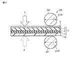
次に、上記積層体等の被評価物の評価に使用する冶具について説明する。
図4に示すように、冶具200は、一対の棒201、202を備えている。棒201、202は、所定の間隔を置いて平行に設けられている。棒201、202の断面形状は円(真円)である。棒201、202の間隔は、調整可能であり、上記被評価物を固定する状態に調整されたり、棒201、202の間に上記被評価物を通すことのできる状態に調整されたりでき得る。また、棒201、202としては、直径の異なる複数種類の棒を取り替えて使用することができる。ここでは、棒201、202の直径を2Rとする。Next, a jig used for evaluating an object to be evaluated such as the laminate will be described.
As shown in FIG. 4, the
図4に示した冶具200を用いて被評価物の可撓性を評価する際、被評価物を棒201、202の間に通し、被評価物を棒201、202で挟んで固定する。そして、被評価物を180°曲げ、被評価物が塑性変形しなかった際の被評価物の最小の曲げ半径を最小曲げRと定義する。そして、最小曲げRの値に基づいて被評価物の可撓性を評価する。 When evaluating the flexibility of the object to be evaluated using the
また、最小曲げRを評価(測定)する際、図の向きで、上方向や下方向に初期応力Fを加えるなどして行う。下向きの最小曲げRを評価する際、下方向に初期応力Fを加えるなどし、被評価物を棒201の半周に密接させることにより、被評価物を下方向に180°曲げることができる。同様に、上向きの最小曲げRを評価する際、上方向に初期応力Fを加えるなどし、被評価物を棒202の半周に密接させることにより、被評価物を上方向に180°曲げることができる。この際、棒201、202の直径を徐々に小さくして被評価物における塑性変形の有無を評価(調査)することにより、最小曲げRを求めることができる。 Further, when evaluating (measuring) the minimum bending R, it is performed by applying an initial stress F upward or downward in the direction shown in the figure. When evaluating the downward minimum bending R, the object to be evaluated can be bent 180 ° downward by bringing the object to be evaluated into close contact with the half circumference of the
図3に示すように、実施例1乃至4の積層体のそれぞれの最小曲げRは、下向き及び上向きの何れにおいても、少なくとも2mmであった。これにより、実施例1乃至4の積層体は、何れも可撓性に優れていることが分かった。 As shown in FIG. 3, the minimum bending R of each of the laminates of Examples 1 to 4 was at least 2 mm in both the downward and upward directions. Thereby, it turned out that all the laminated bodies of Examples 1 to 4 are excellent in flexibility.
また、比較例1の樹脂層10及び比較例2の積層体のそれぞれの最小曲げRは、下向き及び上向きの何れにおいても、少なくとも2mmであった。これにより、比較例1の樹脂層10及び比較例2の積層体は、何れも可撓性に優れていることが分かった。 Further, the minimum bending R of each of the
しかしながら、比較例3の積層体において、下向きの最小曲げRは25mmであり、上向きの最小曲げRは30mmであった。これにより、比較例3の積層体の可撓性は失われていることが分かる。また、下向きの最小曲げRより、上向きの最小曲げRの方が大きい値であることからも、樹脂層10(特に、樹脂層10の表面)に変質が生じ、樹脂層10の可撓性が失われたことが要因であることが分かる。 However, in the laminate of Comparative Example 3, the minimum downward bending R was 25 mm, and the upward minimum bending R was 30 mm. Thereby, it turns out that the flexibility of the laminated body of the comparative example 3 is lost. Further, since the upward minimum bending R is larger than the downward minimum bending R, the resin layer 10 (particularly, the surface of the resin layer 10) is altered and the flexibility of the
上記のように構成された第2の実施形態に係る有機EL表示装置DAによれば、有機EL表示装置DAは、樹脂層10表面上に形成された下地絶縁層11と、スイッチング素子SW1乃至SW3と、を備えている。下地絶縁層11は、第1シリコン酸化膜1、シリコン窒化膜2及び第2シリコン酸化膜3を有している。 According to the organic EL display device DA according to the second embodiment configured as described above, the organic EL display device DA includes the
第1シリコン酸化膜1の厚みが50nmの場合に限らず、上記厚みが10nm、30nm及び100nmの何れの場合であっても樹脂層10の可撓性を維持することができる。このため、樹脂層10(有機EL表示装置DA)の可撓性を維持するためには、第1シリコン酸化膜1の厚みが10nm以上100nm以下であると好ましい。 The flexibility of the
なお、樹脂層10(有機EL表示装置DA)の可撓性を維持するため、第1シリコン酸化膜1の厚みが100nmを超えてもよい。但し、第1シリコン酸化膜1を厚くするほど、成膜の長期化を招き、厚みの均一性が失われる結果となる。 In addition, in order to maintain the flexibility of the resin layer 10 (organic EL display device DA), the thickness of the first
その他、第2の実施形態では、上記第1の実施形態で得られる効果と同様の効果を得ることができる。
上記のことから、可撓性及び製品信頼性に優れた有機EL表示装置DAを得ることができる。In addition, in 2nd Embodiment, the effect similar to the effect acquired in the said 1st Embodiment can be acquired.
From the above, the organic EL display device DA having excellent flexibility and product reliability can be obtained.
次に、第3の実施形態に係る表示装置について説明する。本実施形態において、上述した第1の実施形態と同一機能部分には同一符号を付し、その詳細な説明は省略する。
図5に示すように、有機EL表示装置DAは、上述した第1の実施形態と同様に形成されている。有機EL表示装置DAを製造する際、第1シリコン酸化膜1が樹脂層10を完全に覆うように形成されている。なお、図示しないが、第1シリコン酸化膜1だけではなく、第1シリコン酸化膜1、シリコン窒化膜2及び第2シリコン酸化膜3の全てが樹脂層10を完全に覆うように形成されている。第1シリコン酸化膜1の周縁部は、ガラス基板100上に位置し、ガラス基板100に接着されている。第1シリコン酸化膜1の外周縁がガラス基板100の外周縁に所定の間隔(例えば、数mm)を置くように、第1シリコン酸化膜1がガラス基板100上に設けられている。Next, a display device according to a third embodiment will be described. In the present embodiment, the same functional parts as those in the first embodiment described above are denoted by the same reference numerals, and detailed description thereof is omitted.
As shown in FIG. 5, the organic EL display device DA is formed in the same manner as in the first embodiment described above. When manufacturing the organic EL display device DA, the first
上記のように構成された第3の実施形態に係る有機EL表示装置DAによれば、有機EL表示装置DAは、樹脂層10表面上に形成された下地絶縁層11と、スイッチング素子SW1乃至SW3と、を備えている。下地絶縁層11は、第1シリコン酸化膜1、シリコン窒化膜2及び第2シリコン酸化膜3を有している。第3の実施形態に係る有機EL表示装置DAは、上述した第1の実施形態に係る有機EL表示装置DAと同様に形成されている。このため、第3の実施形態では、上記第1の実施形態で得られる効果と同様の効果を得ることができる。 According to the organic EL display device DA according to the third embodiment configured as described above, the organic EL display device DA includes the
第1シリコン酸化膜1は樹脂層10を完全に覆うように形成されている。このため、樹脂層10の周縁部においても変質を低減することができる。
第1シリコン酸化膜1の周縁部は、ガラス基板100上に位置している。SiO2は、ガラスとの密着性に優れている。このため、製造工程中における、ガラス基板100から樹脂層10の不所望な剥離を低減することができる。
第1シリコン酸化膜1は、その外周縁が、ガラス基板100の外周縁に所定の間隔を置くように形成されている。このため、ガラス基板100の外周縁、又はその近傍まで第1シリコン酸化膜1等を形成した場合に生じ易くなる第1シリコン酸化膜1等の剥離物(塵)の発生を低減することができる。The first
The peripheral edge of the first
The first
上記のことから、可撓性及び製品信頼性に優れた有機EL表示装置DAを得ることができる。 From the above, the organic EL display device DA having excellent flexibility and product reliability can be obtained.
本発明のいくつかの実施形態を説明したが、これらの実施形態は、例として提示したものであり、発明の範囲を限定することは意図していない。これら新規な実施形態は、その他の様々な形態で実施されることが可能であり、発明の要旨を逸脱しない範囲で、種々の省略、置き換え、変更を行うことができる。これら実施形態やその変形は、発明の範囲や要旨に含まれるとともに、特許請求の範囲に記載された発明とその均等の範囲に含まれる。 Although several embodiments of the present invention have been described, these embodiments are presented by way of example and are not intended to limit the scope of the invention. These novel embodiments can be implemented in various other forms, and various omissions, replacements, and changes can be made without departing from the scope of the invention. These embodiments and modifications thereof are included in the scope and gist of the invention, and are included in the invention described in the claims and the equivalents thereof.
例えば、第2シリコン酸化膜3の厚みは、300nmに限定されるものではなく、種々変形可能である。スイッチング素子SW1乃至SW3(半導体層SC)の電気的特性に悪影響が及ぶことを回避するためは、第2シリコン酸化膜3の厚みが100nm以上500nm以下であると好ましい。また、第2シリコン酸化膜3には、レーザ光が照射されたり、加熱されたりする。上記のことからも、第2シリコン酸化膜3の厚みが100nm以上であると好ましい。 For example, the thickness of the second
なお、第2シリコン酸化膜3の厚みが100nm未満であってもよい。但し、第2シリコン酸化膜3を薄くするほど、スイッチング素子SW1乃至SW3(半導体層SC)の電気的特性に悪影響が及び易くなってしまう。
また、第2シリコン酸化膜3の厚みが500nmを超えてもよい。但し、第1シリコン酸化膜1を厚くするほど、成膜の長期化を招き、厚みの均一性が失われる結果となる。Note that the thickness of the second
Further, the thickness of the second
下地絶縁層11は、樹脂層10に接した第1シリコン酸化膜1と、第1シリコン酸化膜1の上方に形成されたシリコン窒化膜2と、シリコン窒化膜2の上方に形成されスイッチング素子SW1乃至SW3の活性層(半導体層SC)に接する第2シリコン酸化膜3と、の3層積層構造を含んでいれば上述した効果を得ることができる。このため、下地絶縁層11は、上記3層が連続的に積層して形成されていなくともよい。例えば、下地絶縁層11は、第1シリコン酸化膜1と、第1シリコン酸化膜1上に形成されたシリコン窒化膜2と、シリコン窒化膜2上に形成された適当な他の膜(例えば、シリコン酸窒化膜)と、上記適当な他の膜上に形成された第2シリコン酸化膜3と、で形成されていてもよい。 The
下地絶縁層11は、樹脂層10の表面上等、樹脂層表面上に形成されていればよい。例えば、有機EL表示装置DAは、ガラス基板100をさらに備えていてもよい。この場合、ガラス基板100から樹脂層10を剥離すること無しに有機EL表示装置DAを形成すればよい。その他、有機EL表示装置DAは、樹脂層10の変わりにプラスチック基板(樹脂基板)を備えていてもよい。この場合、下地絶縁層11は、プラスチック基板の表面上に形成されていればよい。 The
半導体層SCは、p−Si以外の半導体材料で形成されていてもよい。例えば、半導体層SCは、a−Siで形成されていてもよい。 The semiconductor layer SC may be formed of a semiconductor material other than p-Si. For example, the semiconductor layer SC may be formed of a-Si.
有機EL素子OLED1乃至OLED3の発光色は、白色に限定されるものではなく、例えば赤色、緑色、青色であってもよい。この場合、有機EL表示装置DAは、第1カラーフィルタ31、第2カラーフィルタ32及び第3カラーフィルタ32無しに赤色、緑色、青色の光を発する(表示する)ことができる。 The emission color of the organic EL elements OLED1 to OLED3 is not limited to white, and may be, for example, red, green, or blue. In this case, the organic EL display device DA can emit (display) red, green, and blue light without the
本発明の実施形態は、上述した有機EL表示装置DAへの適用に限定されるものではなく、他の有機EL表示装置(例えば、ボトムエミッション型有機EL表示装置や、RGB個々の発光層を塗り分けにより形成した有機EL装置)や、有機EL表示装置以外の表示装置(例えば、液晶素子や、電気泳動素子を用いた表示装置)にも適用でき得る。例えば、自己発光素子としては、ダイオード(有機ELダイオード)に限定されるものではなく、自己発光可能な様々な表示素子を利用することができる。
以下に、本願出願の当初の特許請求の範囲に記載された発明を付記する。
[1]樹脂層表面上に形成された下地絶縁層と、
前記下地絶縁層を介して前記樹脂層表面の上方に形成された薄膜トランジスタと、を備え、
前記下地絶縁層は、第1シリコン酸化膜と、前記第1シリコン酸化膜の上方に形成されたシリコン窒化膜と、前記シリコン窒化膜の上方に形成された第2シリコン酸化膜の3層積層構造を含む表示装置。
[2]前記下地絶縁層において、前記樹脂層に接する層は前記第1シリコン酸化膜である[1]に記載の表示装置。
[3]前記下地絶縁層において、前記薄膜トランジスタの活性層に接する層は前記第2シリコン酸化膜である[1]に記載の表示装置。
[4]前記薄膜トランジスタの活性層は、ポリシリコンで形成されている[1]に記載の表示装置。
[5]前記第1シリコン酸化膜の厚みは、10nm以上100nm以下である[1]に記載の表示装置。
[6]前記第2シリコン酸化膜の厚みは、100nm以上500nm以下である[1]に記載の表示装置。
The embodiment of the present invention is not limited to the application to the organic EL display device DA described above, and other organic EL display devices (for example, bottom emission type organic EL display devices and RGB individual light emitting layers are coated). The present invention can also be applied to display devices other than organic EL display devices (for example, display devices using liquid crystal elements or electrophoretic elements). For example, the self-luminous element is not limited to a diode (organic EL diode), and various display elements capable of self-luminance can be used.
Hereinafter, the invention described in the scope of claims of the present application will be appended.
[1] a base insulating layer formed on the resin layer surface;
A thin film transistor formed above the surface of the resin layer through the base insulating layer,
The base insulating layer has a three-layer structure of a first silicon oxide film, a silicon nitride film formed above the first silicon oxide film, and a second silicon oxide film formed above the silicon nitride film. Display device.
[2] The display device according to [1], wherein a layer in contact with the resin layer in the base insulating layer is the first silicon oxide film.
[3] The display device according to [1], wherein in the base insulating layer, a layer in contact with an active layer of the thin film transistor is the second silicon oxide film.
[4] The display device according to [1], wherein the active layer of the thin film transistor is formed of polysilicon.
[5] The display device according to [1], wherein the thickness of the first silicon oxide film is not less than 10 nm and not more than 100 nm.
[6] The display device according to [1], wherein the second silicon oxide film has a thickness of 100 nm to 500 nm.
DA…有機EL表示装置、AR…アレイ基板、CT…対向基板、10…樹脂層、11…下地絶縁層、1…第1シリコン酸化膜、2…シリコン窒化膜、3…第2シリコン酸化膜、SW1,SW2,SW3…スイッチング素子、SC…半導体層、OLED1,OLED2,OLED3…有機EL素子、100…ガラス基板、200…冶具。 DA ... organic EL display device, AR ... array substrate, CT ... counter substrate, 10 ... resin layer, 11 ... base insulating layer, 1 ... first silicon oxide film, 2 ... silicon nitride film, 3 ... second silicon oxide film, SW1, SW2, SW3 ... switching element, SC ... semiconductor layer, OLED1, OLED2, OLED3 ... organic EL element, 100 ... glass substrate, 200 ... jig.
Claims (5)
Translated fromJapanese前記下地絶縁層を介して前記樹脂層表面の上方に形成された薄膜トランジスタの活性層と、を備え、
前記下地絶縁層は、第1シリコン酸化膜と、前記第1シリコン酸化膜の上方に形成されたシリコン窒化膜と、前記シリコン窒化膜の上方に形成された第2シリコン酸化膜の3層積層構造を含み、
前記下地絶縁層において、前記樹脂層に接する層は前記第1シリコン酸化膜であり、
前記第1シリコン酸化膜は、前記樹脂層の周縁部まで形成され、
前記樹脂層の下面を除いた上面と周縁面は前記第1シリコン酸化膜で覆われている表示装置。A base insulating layer formed on the surface of the resin layer;
An active layer of a thin film transistor formed above the surface of the resin layer through the base insulating layer,
The base insulating layer has a three-layer structure of a first silicon oxide film, a silicon nitride film formed above the first silicon oxide film, and a second silicon oxide film formed above the silicon nitride film. Including
In the base insulating layer, the layer in contact with the resin layer is the first silicon oxide film,
The first silicon oxide film is formed upto a peripheral edge of the resin layer,
Viewing devicetop and the peripheral surface is covered with the first silicon oxide film excluding the lower surface of the resin layer.
Priority Applications (4)
| Application Number | Priority Date | Filing Date | Title |
|---|---|---|---|
| JP2013216298AJP6322380B2 (en) | 2013-10-17 | 2013-10-17 | Display device |
| US14/513,653US9666599B2 (en) | 2013-10-17 | 2014-10-14 | Display device having a multilayered undercoating layer of silicon oxide and silicon nitride |
| CN201410553294.0ACN104576654B (en) | 2013-10-17 | 2014-10-17 | Display device |
| US15/479,305US10658400B2 (en) | 2013-10-17 | 2017-04-05 | Method of manufacturing display device having a multilayered undercoating layer of silicon oxide and silicon nitride |
Applications Claiming Priority (1)
| Application Number | Priority Date | Filing Date | Title |
|---|---|---|---|
| JP2013216298AJP6322380B2 (en) | 2013-10-17 | 2013-10-17 | Display device |
Publications (2)
| Publication Number | Publication Date |
|---|---|
| JP2015079861A JP2015079861A (en) | 2015-04-23 |
| JP6322380B2true JP6322380B2 (en) | 2018-05-09 |
Family
ID=52825408
Family Applications (1)
| Application Number | Title | Priority Date | Filing Date |
|---|---|---|---|
| JP2013216298AActiveJP6322380B2 (en) | 2013-10-17 | 2013-10-17 | Display device |
Country Status (3)
| Country | Link |
|---|---|
| US (2) | US9666599B2 (en) |
| JP (1) | JP6322380B2 (en) |
| CN (1) | CN104576654B (en) |
Families Citing this family (4)
| Publication number | Priority date | Publication date | Assignee | Title |
|---|---|---|---|---|
| JP6495754B2 (en) | 2015-06-12 | 2019-04-03 | 株式会社ジャパンディスプレイ | Display device |
| JP7126823B2 (en) | 2016-12-23 | 2022-08-29 | 株式会社半導体エネルギー研究所 | Manufacturing method of semiconductor device |
| JP6907032B2 (en)* | 2017-06-06 | 2021-07-21 | 株式会社ジャパンディスプレイ | Display device and its manufacturing method |
| CN109427249A (en)* | 2017-08-31 | 2019-03-05 | 昆山工研院新型平板显示技术中心有限公司 | Flexible display panels and preparation method thereof |
Family Cites Families (14)
| Publication number | Priority date | Publication date | Assignee | Title |
|---|---|---|---|---|
| US5686360A (en)* | 1995-11-30 | 1997-11-11 | Motorola | Passivation of organic devices |
| US5981404A (en)* | 1996-11-22 | 1999-11-09 | United Microelectronics Corp. | Multilayer ONO structure |
| JPH11103064A (en)* | 1997-09-26 | 1999-04-13 | Sharp Corp | Method for manufacturing semiconductor device |
| US6664137B2 (en)* | 2001-03-29 | 2003-12-16 | Universal Display Corporation | Methods and structures for reducing lateral diffusion through cooperative barrier layers |
| KR20050073855A (en) | 2004-01-12 | 2005-07-18 | 삼성전자주식회사 | Flexible display and manufacturing method thereof |
| US7696024B2 (en) | 2006-03-31 | 2010-04-13 | Semiconductor Energy Laboratory Co., Ltd. | Semiconductor device and manufacturing method thereof |
| US7875532B2 (en)* | 2007-06-15 | 2011-01-25 | Semiconductor Energy Laboratory Co., Ltd. | Substrate for manufacturing semiconductor device and manufacturing method thereof |
| JP2009088239A (en)* | 2007-09-28 | 2009-04-23 | Sharp Corp | Semiconductor device and manufacturing method thereof |
| KR101793047B1 (en)* | 2010-08-03 | 2017-11-03 | 삼성디스플레이 주식회사 | flexible display and Method for manufacturing the same |
| JP5647860B2 (en)* | 2010-10-28 | 2015-01-07 | 富士フイルム株式会社 | Thin film transistor and manufacturing method thereof |
| TWI692108B (en)* | 2013-04-10 | 2020-04-21 | 日商半導體能源研究所股份有限公司 | Semiconductor device and manufacturing method thereof |
| KR102090560B1 (en)* | 2013-04-11 | 2020-03-19 | 삼성디스플레이 주식회사 | Apparatus for bending and the method of bending using the same. |
| US9444015B2 (en)* | 2014-06-18 | 2016-09-13 | X-Celeprint Limited | Micro assembled LED displays and lighting elements |
| US9515099B2 (en)* | 2014-07-31 | 2016-12-06 | Lg Display Co., Ltd. | Flexible display device with wire having reinforced portion and manufacturing method for the same |
- 2013
- 2013-10-17JPJP2013216298Apatent/JP6322380B2/enactiveActive
- 2014
- 2014-10-14USUS14/513,653patent/US9666599B2/enactiveActive
- 2014-10-17CNCN201410553294.0Apatent/CN104576654B/enactiveActive
- 2017
- 2017-04-05USUS15/479,305patent/US10658400B2/enactiveActive
Also Published As
| Publication number | Publication date |
|---|---|
| CN104576654B (en) | 2018-02-13 |
| US9666599B2 (en) | 2017-05-30 |
| US10658400B2 (en) | 2020-05-19 |
| JP2015079861A (en) | 2015-04-23 |
| US20170207255A1 (en) | 2017-07-20 |
| US20150108488A1 (en) | 2015-04-23 |
| CN104576654A (en) | 2015-04-29 |
Similar Documents
| Publication | Publication Date | Title |
|---|---|---|
| US10069109B2 (en) | Organic light emitting device and method of fabricating the same | |
| US8637333B2 (en) | Organic light emitting diode display and manufacturing method of the same | |
| US8518285B2 (en) | Substrate section for flexible display device, method of manufacturing the substrate section, and method of manufacturing organic light emitting display device including the substrate | |
| US10374096B2 (en) | Semiconductor device | |
| US9871223B2 (en) | Organic light emitting display device having multiple films | |
| US8574662B2 (en) | Substrate section for flexible display device, method of manufacturing substrate section, and method of manufacturing organic light emitting display device including substrate | |
| US20150236297A1 (en) | Organic light-emitting display apparatus | |
| US9312279B2 (en) | Thin film transistor array substrate, method of manufacturing the same, and display apparatus including the same | |
| US8070546B2 (en) | Laser irradiation apparatus for bonding and method of manufacturing display device using the same | |
| US9331304B2 (en) | Organic light-emitting display device and method of manufacturing the same | |
| US20190096982A1 (en) | Organic light emitting diode display | |
| WO2016052151A1 (en) | Organic el display device, method for manufacturing same, and electronic apparatus | |
| US20120104933A1 (en) | Organic Light Emitting Display Apparatus and Method of Manufacturing the Same | |
| TW201218374A (en) | Organic light-emitting diode display device | |
| US10658400B2 (en) | Method of manufacturing display device having a multilayered undercoating layer of silicon oxide and silicon nitride | |
| US9666428B2 (en) | Display device | |
| KR20160137129A (en) | Thin film transistor, display with the same, and method of fabricating the same | |
| US8502443B2 (en) | Organic light-emitting display apparatus and method of manufacturing the same | |
| JP5049613B2 (en) | Organic light emitting device and manufacturing method thereof | |
| US20150129842A1 (en) | Method For Manufacturing Organic Electroluminescence Device And Organic Electroluminescence Device Manufactured With Same |
Legal Events
| Date | Code | Title | Description |
|---|---|---|---|
| A621 | Written request for application examination | Free format text:JAPANESE INTERMEDIATE CODE: A621 Effective date:20160914 | |
| A977 | Report on retrieval | Free format text:JAPANESE INTERMEDIATE CODE: A971007 Effective date:20170613 | |
| A131 | Notification of reasons for refusal | Free format text:JAPANESE INTERMEDIATE CODE: A131 Effective date:20170620 | |
| A521 | Request for written amendment filed | Free format text:JAPANESE INTERMEDIATE CODE: A523 Effective date:20170801 | |
| A131 | Notification of reasons for refusal | Free format text:JAPANESE INTERMEDIATE CODE: A131 Effective date:20180130 | |
| A521 | Request for written amendment filed | Free format text:JAPANESE INTERMEDIATE CODE: A523 Effective date:20180305 | |
| TRDD | Decision of grant or rejection written | ||
| A01 | Written decision to grant a patent or to grant a registration (utility model) | Free format text:JAPANESE INTERMEDIATE CODE: A01 Effective date:20180327 | |
| A61 | First payment of annual fees (during grant procedure) | Free format text:JAPANESE INTERMEDIATE CODE: A61 Effective date:20180409 | |
| R150 | Certificate of patent or registration of utility model | Ref document number:6322380 Country of ref document:JP Free format text:JAPANESE INTERMEDIATE CODE: R150 | |
| R250 | Receipt of annual fees | Free format text:JAPANESE INTERMEDIATE CODE: R250 | |
| R250 | Receipt of annual fees | Free format text:JAPANESE INTERMEDIATE CODE: R250 | |
| R250 | Receipt of annual fees | Free format text:JAPANESE INTERMEDIATE CODE: R250 | |
| R250 | Receipt of annual fees | Free format text:JAPANESE INTERMEDIATE CODE: R250 | |
| R250 | Receipt of annual fees | Free format text:JAPANESE INTERMEDIATE CODE: R250 | |
| S111 | Request for change of ownership or part of ownership | Free format text:JAPANESE INTERMEDIATE CODE: R313113 | |
| R350 | Written notification of registration of transfer | Free format text:JAPANESE INTERMEDIATE CODE: R350 |