JP6317695B2 - Image sensor and formation method thereof - Google Patents
Image sensor and formation method thereofDownload PDFInfo
- Publication number
- JP6317695B2 JP6317695B2JP2015051669AJP2015051669AJP6317695B2JP 6317695 B2JP6317695 B2JP 6317695B2JP 2015051669 AJP2015051669 AJP 2015051669AJP 2015051669 AJP2015051669 AJP 2015051669AJP 6317695 B2JP6317695 B2JP 6317695B2
- Authority
- JP
- Japan
- Prior art keywords
- filter
- light
- pixel
- image sensor
- wavelength
- Prior art date
- Legal status (The legal status is an assumption and is not a legal conclusion. Google has not performed a legal analysis and makes no representation as to the accuracy of the status listed.)
- Active
Links
Images


Classifications
- H—ELECTRICITY
- H10—SEMICONDUCTOR DEVICES; ELECTRIC SOLID-STATE DEVICES NOT OTHERWISE PROVIDED FOR
- H10F—INORGANIC SEMICONDUCTOR DEVICES SENSITIVE TO INFRARED RADIATION, LIGHT, ELECTROMAGNETIC RADIATION OF SHORTER WAVELENGTH OR CORPUSCULAR RADIATION
- H10F39/00—Integrated devices, or assemblies of multiple devices, comprising at least one element covered by group H10F30/00, e.g. radiation detectors comprising photodiode arrays
- H10F39/80—Constructional details of image sensors
- H10F39/805—Coatings
- H10F39/8053—Colour filters
- G—PHYSICS
- G02—OPTICS
- G02B—OPTICAL ELEMENTS, SYSTEMS OR APPARATUS
- G02B5/00—Optical elements other than lenses
- G02B5/20—Filters
- G02B5/201—Filters in the form of arrays
- G—PHYSICS
- G02—OPTICS
- G02B—OPTICAL ELEMENTS, SYSTEMS OR APPARATUS
- G02B5/00—Optical elements other than lenses
- G02B5/20—Filters
- G02B5/22—Absorbing filters
- H—ELECTRICITY
- H10—SEMICONDUCTOR DEVICES; ELECTRIC SOLID-STATE DEVICES NOT OTHERWISE PROVIDED FOR
- H10F—INORGANIC SEMICONDUCTOR DEVICES SENSITIVE TO INFRARED RADIATION, LIGHT, ELECTROMAGNETIC RADIATION OF SHORTER WAVELENGTH OR CORPUSCULAR RADIATION
- H10F39/00—Integrated devices, or assemblies of multiple devices, comprising at least one element covered by group H10F30/00, e.g. radiation detectors comprising photodiode arrays
- H10F39/011—Manufacture or treatment of image sensors covered by group H10F39/12
- H10F39/024—Manufacture or treatment of image sensors covered by group H10F39/12 of coatings or optical elements
- H—ELECTRICITY
- H10—SEMICONDUCTOR DEVICES; ELECTRIC SOLID-STATE DEVICES NOT OTHERWISE PROVIDED FOR
- H10F—INORGANIC SEMICONDUCTOR DEVICES SENSITIVE TO INFRARED RADIATION, LIGHT, ELECTROMAGNETIC RADIATION OF SHORTER WAVELENGTH OR CORPUSCULAR RADIATION
- H10F39/00—Integrated devices, or assemblies of multiple devices, comprising at least one element covered by group H10F30/00, e.g. radiation detectors comprising photodiode arrays
- H10F39/10—Integrated devices
- H10F39/12—Image sensors
- H10F39/18—Complementary metal-oxide-semiconductor [CMOS] image sensors; Photodiode array image sensors
- H10F39/182—Colour image sensors
- H—ELECTRICITY
- H10—SEMICONDUCTOR DEVICES; ELECTRIC SOLID-STATE DEVICES NOT OTHERWISE PROVIDED FOR
- H10F—INORGANIC SEMICONDUCTOR DEVICES SENSITIVE TO INFRARED RADIATION, LIGHT, ELECTROMAGNETIC RADIATION OF SHORTER WAVELENGTH OR CORPUSCULAR RADIATION
- H10F39/00—Integrated devices, or assemblies of multiple devices, comprising at least one element covered by group H10F30/00, e.g. radiation detectors comprising photodiode arrays
- H10F39/10—Integrated devices
- H10F39/12—Image sensors
- H10F39/18—Complementary metal-oxide-semiconductor [CMOS] image sensors; Photodiode array image sensors
- H10F39/184—Infrared image sensors
- H10F39/1847—Multispectral infrared image sensors having a stacked structure, e.g. NPN, NPNPN or multiple quantum well [MQW] structures
- H—ELECTRICITY
- H10—SEMICONDUCTOR DEVICES; ELECTRIC SOLID-STATE DEVICES NOT OTHERWISE PROVIDED FOR
- H10F—INORGANIC SEMICONDUCTOR DEVICES SENSITIVE TO INFRARED RADIATION, LIGHT, ELECTROMAGNETIC RADIATION OF SHORTER WAVELENGTH OR CORPUSCULAR RADIATION
- H10F39/00—Integrated devices, or assemblies of multiple devices, comprising at least one element covered by group H10F30/00, e.g. radiation detectors comprising photodiode arrays
- H10F39/10—Integrated devices
- H10F39/12—Image sensors
- H10F39/199—Back-illuminated image sensors
- H—ELECTRICITY
- H10—SEMICONDUCTOR DEVICES; ELECTRIC SOLID-STATE DEVICES NOT OTHERWISE PROVIDED FOR
- H10F—INORGANIC SEMICONDUCTOR DEVICES SENSITIVE TO INFRARED RADIATION, LIGHT, ELECTROMAGNETIC RADIATION OF SHORTER WAVELENGTH OR CORPUSCULAR RADIATION
- H10F39/00—Integrated devices, or assemblies of multiple devices, comprising at least one element covered by group H10F30/00, e.g. radiation detectors comprising photodiode arrays
- H10F39/80—Constructional details of image sensors
- H10F39/806—Optical elements or arrangements associated with the image sensors
- H10F39/8063—Microlenses
Landscapes
- Physics & Mathematics (AREA)
- General Physics & Mathematics (AREA)
- Optics & Photonics (AREA)
- Solid State Image Pick-Up Elements (AREA)
- Optical Filters (AREA)
- Transforming Light Signals Into Electric Signals (AREA)
- Color Television Image Signal Generators (AREA)
- Spectroscopy & Molecular Physics (AREA)
Description
Translated fromJapanese本発明は、イメージセンサーに関するものであって、特に、3D検出撮像応用、たとえば、飛行時間型(ToF)技術の純粋な赤外線(IR)信号を収集することができるイメージセンサーに関するものである。 The present invention relates to image sensors, and in particular to image sensors capable of collecting pure infrared (IR) signals in 3D detection imaging applications, such as time-of-flight (ToF) technology.
現在、飛行時間型(ToF)技術は、広く、近代産業に用いられて、調整された光源と共に、相補型MOS(CMOS)画素アレイを用いて、3次元(3D)撮像を提供する。3D TOF カメラは、すでに、多くの異なるアプリケーション、たとえば、製造された商品のプロファイル検査、コンピューター支援設計(CAD)検証、地理測量、および、物体撮像に用いられている。 Currently, time-of-flight (ToF) technology is widely used in the modern industry to provide three-dimensional (3D) imaging using a complementary MOS (CMOS) pixel array with a conditioned light source. 3D TOF cameras are already used in many different applications, such as profile inspection of manufactured goods, computer aided design (CAD) verification, geogrammetry, and object imaging.
3D ToFカメラの操作は、調整された光源を使用して、シーンを照射し、反射した光線を監視する。照明と反射間の位相シフトが測定され、距離に変換される。一般に、シーンを照射する調整された光源は、約850nmの近赤外線で操作する固体レーザー、または、発光ダイオード(LED)によるもので、不可視である。調整された光源の同一スペクトルに対応するように設計された画像センサーは、光線を受信して、フォトニックエネルギーを電流に転換して、シーンの距離(深さ)情報を得る。 The operation of the 3D ToF camera uses a conditioned light source to illuminate the scene and monitor the reflected rays. The phase shift between illumination and reflection is measured and converted to distance. In general, the tuned light source that illuminates the scene is invisible, either by a solid state laser operating at about 850 nm near infrared, or a light emitting diode (LED). An image sensor designed to correspond to the same spectrum of the tuned light source receives the light and converts photonic energy into current to obtain scene distance (depth) information.
しかし、画像センサーから入る光線は、環境成分と反射成分を有する。距離(深さ)情報は、反射成分中だけに組み込まれている。よって、環境成分は、距離(深さ)情報の信号対ノイズ比(SNR)を減少させる。 However, light rays that enter from the image sensor have an environmental component and a reflection component. The distance (depth) information is incorporated only in the reflection component. Thus, the environmental component reduces the signal-to-noise ratio (SNR) of the distance (depth) information.
本発明は、イメージセンサーとその形成方法を提供する。 The present invention provides an image sensor and a method for forming the image sensor.
本発明は、赤色(R)、緑色(G)、および、青色(B)画素と赤外線(IR)画素を、単一イメージセンサーに整合したイメージセンサーを提供する。イメージセンサーにおいて、R、G、および、B信号は、R、G、および、B画素に位置するフォトダイオードから得られ、IR信号は、IR画素に位置するフォトダイオードから得られる。しかし、IR光が、R、G、および、B画素に位置するフォトダイオードにより受信されるとき、IR信号ノイズが、R、G、および、B画素のフォトダイオードから生成される。本発明のイメージセンサーは、R、G、および、B画素中に設置されるIRフィルターを有して、R、G、および、B画素に位置するフォトダイオードから生成されるIR信号ノイズを回避する。よって、本発明のイメージセンサーは、IR画素に位置するフォトダイオードから、純粋なIR信号収集を得て、IR信号ノイズがない、または、R、G、および、B画素で、わずかに低いIR信号ノイズが発生する。これにより、イメージセンサーの距離(深さ)情報の信号対ノイズ比(SNR)が増加する。 The present invention provides an image sensor in which red (R), green (G), and blue (B) pixels and infrared (IR) pixels are matched to a single image sensor. In the image sensor, R, G, and B signals are obtained from photodiodes located in R, G, and B pixels, and IR signals are obtained from photodiodes located in IR pixels. However, when IR light is received by photodiodes located in the R, G, and B pixels, IR signal noise is generated from the photodiodes of the R, G, and B pixels. The image sensor of the present invention has an IR filter installed in the R, G, and B pixels, and avoids IR signal noise generated from photodiodes located in the R, G, and B pixels. . Thus, the image sensor of the present invention obtains a pure IR signal collection from the photodiode located in the IR pixel and has no IR signal noise or slightly lower IR signal at the R, G and B pixels. Noise is generated. This increases the signal to noise ratio (SNR) of the distance (depth) information of the image sensor.
いくつかの実施態様によると、イメージセンサーが提供される。イメージセンサーは、赤色(R)画素、緑色(G)画素、青色(B)画素、および、赤外線(IR)画素を含む。R、G、および、Bフィルターは、それぞれ、R、G、および、B画素中に設置される。IRパスフィルターはIR画素中に設置される。IRフィルターは、R、G、および、Bフィルターと重ねられ、IRフィルターは、少なくとも特定波長を有するIR光を遮断する。 According to some embodiments, an image sensor is provided. The image sensor includes a red (R) pixel, a green (G) pixel, a blue (B) pixel, and an infrared (IR) pixel. The R, G, and B filters are installed in the R, G, and B pixels, respectively. The IR pass filter is installed in the IR pixel. The IR filter is overlapped with the R, G, and B filters, and the IR filter blocks at least IR light having a specific wavelength.
いくつかの実施態様によると、イメージセンサーの形成方法が提供される。本方法は、複数のフォトダイオードを含み、各フォトダイオードが、赤色(R)画素、緑色(G)画素、青色(B)画素と赤外線(IR)画素の一画素中に設置される半導体基板を供給する工程と、半導体基板上に、IRフィルター材料層を形成する工程と、IR画素に位置するIRフィルター材料層の一部を除去して、IRフィルターを形成し、IRフィルターが、少なくとも特定波長を有するIR光を遮断し、IRフィルターが、IR画素で、開口を有する工程と、R、G、および、B画素で、それぞれ、R、G、および、Bフィルターを形成する工程と、IR画素に位置するIRフィルターの開口中に、IRパスフィルターを形成する工程と、を含む。 According to some embodiments, a method for forming an image sensor is provided. The method includes a plurality of photodiodes, each of which includes a semiconductor substrate disposed in one pixel of a red (R) pixel, a green (G) pixel, a blue (B) pixel, and an infrared (IR) pixel. A step of supplying, a step of forming an IR filter material layer on the semiconductor substrate, a part of the IR filter material layer located in the IR pixel is removed to form an IR filter, and the IR filter has at least a specific wavelength. And a process of forming an R, G, and B filter in each of the R, G, and B pixels, and an IR pixel. Forming an IR pass filter in the opening of the IR filter located at.
本発明のイメージセンサーによると、イメージセンサーの距離(深さ)情報の信号対ノイズ比(SNR)が増加する。 According to the image sensor of the present invention, the signal-to-noise ratio (SNR) of the distance (depth) information of the image sensor is increased.
上記及び他の目的及び本発明の特徴は、添付図面とともに以下の記載を参照することにより明らかとなる。 These and other objects and features of the present invention will become apparent from the following description taken in conjunction with the accompanying drawings.
本発明の目的と利点は添付請求項に具体的に記載されている要素及び組合せによって実現、達成されるであろう。なお、上述の一般的な説明と、以下に述べる詳細な説明は具体例であって、例示だけを目的としており、特許請求されている本発明の範囲の限定を意図するものではない。 The objects and advantages of the invention will be realized and attained by means of the elements and combinations particularly pointed out in the appended claims. It should be noted that the above general description and the detailed description given below are specific examples, which are for illustrative purposes only and are not intended to limit the scope of the claimed invention.
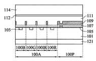
図1を参照すると、いくつかの実施形態による裏面照明(BSI)イメージセンサー100の一部の断面が示される。イメージセンサー100は、複数の画素を含み、赤色(R)画素100R、緑色(G)画素100G、青色(B)画素100Bと赤外線(IR)画素100IRが配列されて、画素アレイ領域100A中でアレイを形成している。イメージセンサー100の周辺領域100Pは、画素アレイ領域100Aを囲む。イメージセンサー100は、複数のフォトダイオード103を含む半導体基板101を含む。各フォトダイオード103は、赤色(R)画素100R、緑色(G)画素100G、青色(B)画素100Bと赤外線(IR)画素100IRの一つ画素中に設置される。 Referring to FIG. 1, a cross section of a portion of a backside illuminated (BSI)
BSIイメージセンサー100は、さらに、半導体基板101表面上に形成される配線層121を含む。配線層121が、フォトダイオード103下に設置される。配線層121は、金属層間に設置されるいくつかの金属層といくつかの誘電層からなる。金属層と誘電層は、従来の半導体集積回路処理技術により形成される。図を簡潔にするため、図1中では、金属層と誘電層は示されない。配線層121は複数の回路領域を含み、各回路領域は一つのフォトダイオード103に対応する。いくつかの実施形態において、イメージセンサー100は、単一イメージセンサー中に一緒に整合されるR、G、B、および、IR画素を有するCMOSイメージセンサー(CIS)である。 The
いくつかの実施形態において、イメージセンサー100は、さらに、半導体基板101の別の表面上に形成される高誘電率膜105を含み、フォトダイオード103上に設置されている。そのうえ、パッシベーション膜107が高誘電率膜105上に形成される。イメージセンサー100は、さらに、パッシベーション膜107上に形成される遮光分割膜109を有する。遮光分割膜109は、イメージセンサー100の二つの隣接する画素間に設置される複数の仕切りを有し、クロストークを回避する。また、遮光分割膜109は、仕切り間に複数の開口を有する。さらに、イメージセンサー100は、遮光分割膜109を被覆すると共に、遮光分割膜109の開口を充填する別のパッシベーション膜111を有する。 In some embodiments, the
イメージセンサー100は、それぞれ、R、G、および、B画素100R、100G、および、100Bに設置されるRフィルター117R、Gフィルター117G、および、Bフィルター117Bを含む。イメージセンサー100は、さらに、R、G、および、B画素100R、100G、および、100B中に設置され、R、G、および、Bフィルター117R、117G、および、117Bと積み重ねられるIRフィルター115を有する。本発明の実施形態によると、IRフィルター115は、少なくとも特定波長を有するIR光を遮断する。 The
いくつかの実施形態において、IRフィルター115は、特定波長を有するIR光だけを遮断する選択的IRフィルターである。別の実施形態において、IRフィルター115は、IRバンド全体の波長を有するIR光を遮断することができるIRカットオフフィルターである。本発明の実施形態によると、IRフィルター115と結合されるR、G、および、Bフィルター117R、117G、および、117Bは、可視帯内の波長を有するR、GとB光を通過させると共に、少なくとも特定波長を有するIR光を遮断することができる。IRフィルター115により遮断されるIR光の特定波長が以下の記述により説明される。 In some embodiments, the
図1の実施形態において、R、G、および、Bフィルター117R、117G、および、117Bが、IRフィルター115上に設置される。イメージセンサー100は、さらに、R、G、および、B画素100R、100G、および、100Bで、パッシベーション膜111上に形成されるパターン化されたバッファ層113を含む。パターン化されたバッファ層113は、IR画素100IRに開口を有する。IRフィルター115が、パターン化されたバッファ層113上に形成される。IRフィルター115は、さらに、IR画素100IRに開口を有する。図1の実施形態において、パターン化されたバッファ層113が、IRフィルター115の形成のために、エッチング停止層として用いられる。 In the embodiment of FIG. 1, R, G, and B filters 117R, 117G, and 117B are installed on the
イメージセンサー100は、さらに、IR画素100IRに設置されるIRパスフィルター119を含む。IRパスフィルター119は、IRバンド中の波長を有するIR光を通過させる。IRパスフィルター119は、IR画素100IRで、第一パッシベーション層111上に形成される。また、IRパスフィルター119が、IR画素100IRに位置するパターン化されたバッファ層113、IRフィルター115とR、G、および、Bフィルター117R、117G、および、117Bの開口に充填される。IRパスフィルター119は、IRフィルターの上面より高い上面を有する。いくつかの実施形態において、IRパスフィルター119の上面は、R、G、および、Bフィルター117R、117G、および、117Bの上面と同一高さである。別の実施形態において、IRパスフィルター119の上面は、R、G、および、Bフィルター117R、117G、および、117Bの上面より低い、または、高い。図1に示されるように、IRパスフィルター119は、さらに、イメージセンサー100の周辺領域100P中に設置される。周辺領域100P中のIRパスフィルター119は遮光効果を有し、且つ、遮光素子として用いられる。 The
図1に示されるように、イメージセンサー100は、さらに、R、G、および、Bフィルター117R、117G、および、117BとIRパスフィルター119上に設置されるマイクロレンズ構造123を含む。そのうえ、イメージセンサー100は、マイクロレンズ構造123上に設置されるダブルバンドパスフィルター125を有する。ダブルバンドパスフィルター125は、可視帯内の第一波長を有する光線、および、特定IRバンドの第二波長を有する光線を通過させることができる。特定IRバンドの第二波長は後に説明する。ダブルバンドパスフィルター125下に設置されるイメージセンサー100の素子は、画像センサー装置ユニット130と称される。 As shown in FIG. 1, the
図2を参照すると、本発明のいくつかの実施形態による物体129を撮像するイメージセンサー100の配置を説明する図である。図2に示されるように、イメージセンサー100は、さらに、光源ユニット127を有し、特定バンドの波長を有するIR光128を、物体129に照射するように配置される。いくつかの実施形態において、光源ユニット127のIR光128の特定バンドの波長は、図1のイメージセンサー100のIRフィルター115により遮断されるIR光の特定波長と一致する。さらに、光源ユニット127のIR光128の特定バンドの波長も、ダブルバンドパスフィルター125の特定IRバンドの第二波長と一致する。いくつかの実施形態において、光源ユニット127は、約 850nmの近赤外線内で操作するLEDである。よって、IRフィルター115により遮断されるIR光の特定波長は約 850nmである。また、ダブルバンドパスフィルター125の特定IRバンドの第二波長は約 850nmである。 Referring to FIG. 2, a diagram illustrating an arrangement of an
図2に示されるように、物体129により反射されるIR光128’が、ダブルバンドパスフィルター125から画像センサー装置ユニット130を通過する。ダブルバンドパスフィルター125の特定IRバンドの第二波長は、光源ユニット127のIR光128の特定バンドの波長と一致するので、ダブルバンドパスフィルター125から画像センサー装置ユニット130を通過した後のIR光128”も、光源ユニット127のIR光128の波長と同じ波長を有する。 As shown in FIG. 2, the IR light 128 ′ reflected by the
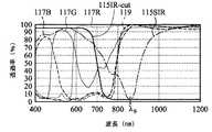
再度、図1を参照すると、IR光128”が、IRパスフィルター119により通過すると共に、IR画素100IRで、フォトダイオード103により受信されて、物体129の深さ情報のIR信号を得る。一方、図3を参照すると、本発明のいくつかの実施形態による、それぞれ、イメージセンサー100Rフィルター117R、Gフィルター117G、Bフィルター117B、IRパスフィルター119、選択的IRフィルター115SIRとIRカットオフフィルター 115IR-cutの光学特性を説明する透過率対波長のグラフである。図3に示されるように、可視光は、R、G、および、Bフィルター117R、117G、および、117Bを通過して、可視帯で、R、G、および、B信号を生成することができる。さらに、700nmから1200nmのIRバンドの波長を有するIR光も、高透過率で、R、G、および、Bフィルター117R、117G、および、117Bを通過することができる。よって、R、G、および、B信号が、IRバンドの波長、たとえば、700nm〜1200nmで生成される。よって、IR光128”も、R、G、および、Bフィルター117R、117G、および、117Bを通過する。IR光128”は、R、G、および、B画素で、フォトダイオード103により受信される場合、IR信号ノイズが生成される。 Referring again to FIG. 1, IR light 128 ″ passes through the
本発明の実施形態によると、少なくとも特定波長を有するIR光を遮蔽することができ、光源ユニット127のIR光128の波長と同じであるIRフィルター115は、R、G、および、Bフィルター117R、117G、および、117Bと積み重ねられる。よって、IR光128”は、IRフィルター115により遮蔽される。R、G、および、B画素中のフォトダイオード103は、IR光を受信しない、または、低透過率のIR光だけを受信する。その結果、IR信号ノイズが、イメージセンサー100で生成されるのを防止することができる。言い換えれば、イメージセンサー100は、純粋なIR信号を収集することができる。 According to the embodiment of the present invention, the
図2に示されていないが、自然光、または、別の光源からの可視光も、物体129により反射されて、反射する可視光を生成する。反射する可視光は、ダブルバンドパスフィルター125から、画像センサー装置ユニット130に通過する。その後、反射した可視光は、R、G、および、Bフィルター117R、117G、および、117Bにより通過して、R、G、および、B画素100R、100G、および、100Bで、フォトダイオード103により受信されて、物体129のカラーイメージ情報のR、G、および、B信号を得る。 Although not shown in FIG. 2, natural light or visible light from another light source is also reflected by the
この実施形態において、IRフィルター115は、R、G、および、Bフィルター117R、117G、および、117Bと重ねられる。IRフィルター115は、可視帯の波長を有する光線を通過させると共に、IRバンド中の特定波長を有する光線を遮蔽することができる。いくつかの実施形態において、IRフィルター115は、図3の選択的IRフィルター115SIRで、IRバンドの特定波長λsを有する光線だけを遮蔽する。選択的IRフィルター115SIRの特定波長λsは、光源ユニット127のIR光128の波長と一致し、たとえば、約850nmである。別の実施形態において、IRフィルター115は、図3のIRカットオフフィルター115IR-cutで、IRバンド全体、たとえば、700nm〜1200nm以上の波長を有する光線を遮蔽する。よって、IRフィルター115と結合されるR、G、および、Bフィルター117R、117G、および、117Bは、可視帯内の波長を有する光線を通過させ、および、特定波長λsを有するIR光を遮蔽することができる。その結果、R、G、および、B画素のフォトダイオード103からIR信号ノイズが生成されないか、生成されても低い。 In this embodiment, the
図3に示されるように、いくつかの実施形態において、IRパスフィルター119は、たとえば、800nm〜1200nm以上のIRバンド中の波長を有するIR光を通過させる。IR信号は、IR画素に位置するフォトダイオード103からのみ得られる。よって、本発明の実施形態によるイメージセンサー100は、純粋なIR信号収集を達成することができる。 As shown in FIG. 3, in some embodiments, the
図4Aは、R、G、および、B画素にIRフィルターがないイメージセンサーのR、G、および、B画素に位置するフォトダイオードから得られるR、G、および、B信号を説明する透過率対波長のグラフである。図4Aに示されるように、R、G、および、B信号は、IRバンドの特定波長λsで、高透過率T1を有する。特定波長λsは、光源ユニットのIR光の特定バンドの波長と一致する。IRバンドの特定波長λsの高透過率T1は、R、G、および、B画素で、フォトダイオードにより受信され、IR信号ノイズを生じる。透過率T1は、約95%〜約15%である。 FIG. 4A is a transmission pair illustrating the R, G, and B signals obtained from a photodiode located in the R, G, and B pixels of an image sensor that does not have an IR filter in the R, G, and B pixels. It is a graph of a wavelength. As shown in FIG. 4A, the R, G, and B signals have a high transmittance T1 at a specific wavelength λs in the IR band. The specific wavelength λs matches the wavelength of the specific band of the IR light of the light source unit. The high transmittance T1 of the specific wavelength λs in the IR band is received by the photodiode in the R, G, and B pixels, and causes IR signal noise. The transmittance T1 is about 95% to about 15%.
図4Bは、本発明のいくつかの実施形態によるR、G、および、B画素に、IRフィルター115があるイメージセンサー100のR、G、および、B画素に位置するフォトダイオードから得られるR、G、および、B信号を説明する透過率対波長のグラフである。図4Bに示されるように、IRバンドの特定波長λsで、低透過率T2を有する。特定波長λsは、図2の光源ユニット127のIR光128の特定バンドの波長と一致する。IRフィルター115は、R、G、および、B画素で、R、G、および、Bフィルターを通過するIR光を遮断する。よって、R、G、および、B画素のフォトダイオードは、IR光を受信しないか、または、低透過率T1のIR光だけを受信する。イメージセンサー100のR、G、および、B画素のフォトダイオードから生成されるIR信号ノイズはないか、または低い。いくつかの実施形態において、透過率T2は、約0%〜約2%である。 FIG. 4B illustrates the R, G, and B pixels obtained from photodiodes located in the R, G, and B pixels of the
図5を参照すると、本発明のいくつかの実施形態による裏面照明(BSI)イメージセンサー100の一部の断面が示される。図5と図1のイメージセンサー100間のひとつの差異は、図5のR、G、および、Bフィルター117R、117G、および、117Bが、IRフィルター115の下に設置されることである。そのうえ、図5のパッシベーション層111上に形成されるパターン化されたバッファ層がない。図5の実施形態において、IRパスフィルター119が、IR画素100IR中に設置されると共に、R、G、および、Bフィルター117R、117G、および、117Bの開口中に充填される。いくつかの実施形態において、図5に示されるように、IRパスフィルター119は、IRフィルターの上面より低い上面を有し、キャビティ120がIRパスフィルター119上に形成される。マイクロレンズ構造123の形成材料が、さらに、IRパスフィルター119上に形成されるキャビティ120中に充填される。別の実施形態において、IRパスフィルター119の上面は、IR光を遮蔽するのに必要なIRフィルター115の厚さに基づいて、IRフィルター115の上面と同じか、または、それより高い。 Referring to FIG. 5, a cross section of a portion of a backside illuminated (BSI)
図5の実施形態において、R、G、および、Bフィルター117R、117G、および、117B上に設置されるIRフィルター115は、まず、少なくとも特定波長を有するIR光を遮蔽し、可視帯の波長を有する光線を通過させる。IRフィルター115により遮蔽されるIR光の特定波長は、図2に示されるイメージセンサー100の光源ユニット127からのIR光128の特定バンドの波長と一致する。よって、IR信号ノイズがないか、または、低IR信号ノイズが、イメージセンサー100のR、G、および、B画素に位置するフォトダイオード103から生成される。イメージセンサー100は、IR画素100IRに位置するフォトダイオード103から、純粋なIR信号を収集することができ、ノイズが発生しない。 In the embodiment of FIG. 5, the
図6A〜図6Dは、いくつかの実施形態による図1のイメージセンサーを製造するいくつかの中間段階100を説明する断面図である。図6Aを参照すると、複数のフォトダイオード103を含む半導体基板101が提供される。各フォトダイオード103が、赤色(R)画素100R、緑色(G)画素100G、青色(B)画素100Bと赤外線(IR)画素100IRの一つの画素中に設置される。配線層121が、半導体基板101表面に形成され、フォトダイオード103下に設置される。いくつかの金属層といくつかの誘電層からなる配線層121は、従来の半導体集積回路処理技術により形成される。 6A-6D are cross-sectional views illustrating several
高誘電率膜105が、半導体基板101の別の表面上に形成され、フォトダイオード103上に設置される。パッシベーション膜107が高誘電率膜105上に形成される。遮光分割膜109がパッシベーション膜107上に形成される。遮光分割膜109は、イメージセンサー100の二つの隣接する画素間に設置される複数の仕切りを有し、クロストークを回避する。そのうえ、別のパッシベーション層111が形成されて、遮光分割膜109を被覆すると共に、遮光分割膜109の開口中に充填される。 A high dielectric
図6Aに示されるように、バッファ材料層112がパッシベーション膜111上に形成される。バッファ材料層112が、コーティングプロセスにより、パッシベーション層111上に形成される。次に、IRフィルター材料層114が、画素アレイ領域100A中のバッファ材料層112上に形成される。IRフィルター材料層114がコーティングプロセスにより形成される。 As shown in FIG. 6A, a
図6Bを参照すると、IR画素100IRのIRフィルター材料層114の一部が、バッファ材料層112をエッチング停止層として用いることにより、エッチングプロセスで除去されて、IRフィルター115を形成する。その後、IR画素100IRのバッファ材料層112の一部が、別のエッチングプロセスにより除去されて、パターン化されたバッファ層113を形成する。よって、開口116は、パターン化されたバッファ層113とIRフィルター115中に形成される。上述したように、IRフィルター115は、少なくとも特定波長を有するIR光を遮断する。 Referring to FIG. 6B, a portion of the IR
図6Cを参照すると、Rフィルター117R、Gフィルター117GとBフィルター117Bが、それぞれ、R、G、および、B画素100R、100G、および100Bで、IRフィルター115上に形成される。いくつかの実施形態において、R、G、および、Bフィルター117R、117G、および、117Bが、コーティングとフォトリソグラフィにより形成される。 Referring to FIG. 6C, an
図6Dを参照すると、IRパスフィルター119が、IRフィルター115とパッシベーション膜111の開口112と116中に形成される。さらに、IRパスフィルター119は、さらに、周辺領域100P中のパッシベーション膜111上に形成される。いくつかの実施形態において、IRパスフィルター119が、コーティングプロセスにより形成されて、R、G、および、Bフィルター117R、117G、および、117Bの上面と同一表面の上面を有する。別の実施形態において、IRパスフィルター119が形成されて、R、G、および、Bフィルター117R、117G、および、117Bの上面より低いか、または、高い上面を有する。 Referring to FIG. 6D, an
次に、マイクロレンズ構造123が、R、G、および、Bフィルター117R、117G、および、117BとIRパスフィルター119上に形成される。その後、ダブルバンドパスフィルター125が提供されて、マイクロレンズ構造123上に設置されて、図1のイメージセンサー100を完成する。 Next, a
図7A〜図7Dは、本発明のいくつかの実施形態による図5のイメージセンサー100を製造するいくつかの中間段階を説明する断面図である。図7Aを参照すると、複数のフォトダイオード103を含む半導体基板101、配線層121、高誘電率膜105、パッシベーション膜107、遮光分割膜109とパッシベーション膜111が、図6Aの記述と同じ方法で形成される。この実施形態において、パッシベーション膜111上に形成されるパターン化されたバッファ層がない。 7A-7D are cross-sectional views illustrating several intermediate stages of manufacturing the
図7Aに示されるように、Rフィルター117R、Gフィルター117GとBフィルター117Bが、それぞれ、R、G、および、B画素100R、100G、および、100Bで、パッシベーション膜111上に形成される。いくつかの実施形態において、コーティングとフォトリソグラフィプロセスにより、R、G、および、Bフィルター117R、117G、および、117Bが形成される。IR画素100IRで、R、G、および、Bフィルター117R、117G、および、117B中に形成される開口118がある。 As shown in FIG. 7A, an
図7Bを参照すると、IRフィルター材料層114が、R、G、および、Bフィルター117R、117G、および、117B上に形成されると共に、IR画素100IRで、開口118中を充填する。IRフィルター材料層114はコーティングプロセスにより形成される。 Referring to FIG. 7B, an IR
図7Cを参照すると、IR画素100IRのIRフィルター材料層114の一部が、エッチングプロセスにより除去されて、IRフィルター115を形成する。よって、開口131が、IRフィルター115中とR、G、および、Bフィルター117R、117G、および、117B中に形成される。上述のように、IRフィルター115は、少なくとも特定波長を有するIR光を遮蔽する。 Referring to FIG. 7C, a portion of the IR
図7Dを参照すると、IRパスフィルター119がパッシベーション膜111上に形成されると共に、IR画素100IRに位置するIRフィルター115、および、R、G、および、Bフィルター117R、117G、および、117Bの開口131中に充填される。さらに、IRパスフィルター119は、さらに、周辺領域100P中のパッシベーション膜111上に形成される。いくつかの実施形態において、IRパスフィルター119がコーティングプロセスにより形成されて、IRフィルターの上面より低い上面を有する。よって、IRフィルター115上に形成されるキャビティ120を有する。別の実施形態において、IRパスフィルター119が形成されて、IRフィルターの上面と同じか、または、それより高い表面を有する。 Referring to FIG. 7D, the
次に、マイクロレンズ構造123が、IRフィルター115とIRパスフィルター119上に形成される。いくつかの実施形態において、キャビティ120がIRフィルター115上に形成される。よって、マイクロレンズ構造123の形成材料が、キャビティ120中にも充填される。その後、ダブルバンドパスフィルター125が提供されて、マイクロレンズ構造123上に設置され、図5のイメージセンサー100が完成する。 Next, a
図1と図5の実施形態において、イメージセンサー100は、裏面照明(BSI)イメージセンサーである。別の実施形態において、本発明のイメージセンサーは表面照明(FSI)イメージセンサーである。FSIイメージセンサーにおいて、図1と図5の配線層121は、フォトダイオード103上に設置される。さらに、図1と図5の高誘電率膜105、パッシベーション膜107、遮光分割膜109とパッシベーション膜111は省略することができる。FSIイメージセンサーの別の素子、たとえば、パターン化されたバッファ層113、IRフィルター115、R、G、および、Bフィルター117R、117G、および、117B、IRパスフィルター119、マイクロレンズ構造123とダブルバンドパスフィルター125は、図1と図5のBSIイメージセンサー100と同じである。 In the embodiment of FIGS. 1 and 5, the
本発明では好ましい実施例を前述の通り開示したが、これらは決して本発明に限定するものではなく、当該技術を熟知する者なら誰でも、本発明の精神と領域を脱しない範囲内で各種の変動や潤色を加えることができ、従って本発明の保護範囲は、特許請求の範囲で指定した内容を基準とする。 In the present invention, preferred embodiments have been disclosed as described above. However, the present invention is not limited to the present invention, and any person who is familiar with the technology can use various methods within the spirit and scope of the present invention. Variations and moist colors can be added, so the protection scope of the present invention is based on what is specified in the claims.
100〜イメージセンサー
100A〜画素アレイ領域
100P〜周辺領域
100R〜赤色画素
100G〜緑色画素
100B〜青色画素
100IR〜赤外線画素
101〜半導体基板
103〜フォトダイオード
105〜高誘電率膜
107、111〜パッシベーション層
109〜遮光分割層
112〜バッファ材料層
113〜パターン化されたバッファ層
114〜IRフィルター材料層
115〜IRフィルター
116、118、131〜開口
115SIR〜選択的IRフィルター
115IR-cut〜IRカットオフフィルター
117R〜Rフィルター
117G〜緑フィルター
117B〜青フィルター
119〜IRパスフィルター
120〜キャビティ
121〜配線層
123〜マイクロレンズ構造
125〜ダブルバンドパスフィルター
127〜光源ユニット
128、128’、128”〜IR光
129〜物体
130〜画像センサー装置ユニット
λS〜特定波長
100 to image
Claims (6)
Translated fromJapaneseそれぞれ、前記R、G、および、B画素中に設置されるR、G、および、Bフィルターと、
上面が前記R、G、および、Bフィルターの上面より高く、前記IR画素に設置されるIRパスフィルターと、
前記R、G、および、Bフィルターの上に設置され、少なくとも特定波長を有するIR光を遮蔽するIRフィルターと、
前記IRフィルターと前記IRパスフィルター上に設置されるマイクロレンズ構造を含み、
前記IRパスフィルターの上面は、前記IRフィルターの上面より低く、
前記IRパスフィルター上に設置されるマイクロレンズ構造の底面は、前記IRフィルターの上面より低いこと特徴とするイメージセンサー。A red (R) pixel, a green (G) pixel, a blue (B) pixel and an infrared (IR) pixel;
R, G, and B filters respectively installed in the R, G, and B pixels;
An IR pass filter that hasan upper surface higher than the upper surfaces of the R, G, and B filters and is installed in the IR pixel;
An IR filterthat is installed on the R, G, and B filters and shields at least IR light having a specific wavelength;
A microlens structure installed on the IR filter and the IR pass filter;
The top surface of the IR-pass filter,rather low than the upper surface of the IRfilter,
An image sensor, wherein a bottom surface of a microlens structure installed on the IR pass filter is lower than a top surface of the IR filter .
前記ダブルバンドパスフィルターは、可視帯の第一波長を有する光線、および、特定IRバンドの第二波長を有する光線を通過させ、前記特定IRバンドの前記第二波長は、前記光源ユニットの前記IR光の前記特定波長と一致することを特徴とする請求項2に記載のイメージセンサー。A double band pass filter installed on the microlens structure;
The double band pass filter passes light having a first wavelength in the visible band and light having a second wavelength in a specific IR band, and the second wavelength in the specific IR band is the IR of the light source unit. The image sensor according to claim2 , wherein the image sensor matches the specific wavelength of light.
前記R、G、および、B画素に、それぞれ、R、G、および、Bフィルターを、前記R、G、および、Bフィルターで開口を有するように形成する工程と、
前記R、G、および、Bフィルター上、および、前記開口の中と上部に、IRフィルター材料層を形成する工程と、
前記IRフィルター材料層のうち、前記IR画素に位置する部分を除去して、IRフィルターを形成し、前記IRフィルターは、少なくとも特定波長を有するIR光を遮蔽し、前記IRフィルターが、前記IR画素で、開口を有する工程と、
前記IR画素で、前記IRフィルターの前記開口中に、IRパスフィルターを形成し、前記IRパスフィルターの上面は、前記IRフィルターの上面より低く、キャビティが前記IRパスフィルター上に形成される工程と、
前記IRフィルターと前記IRパスフィルター上にマイクロレンズ構造を形成し、前記マイクロレンズ構造が、前記IRパスフィルター上に形成される前記キャビティ中に充填される工程と、
を含むことを特徴とするイメージセンサーの形成方法。Each of the photodiodes includes a plurality of photodiodes, and each photodiode supplies a semiconductor substrate installed in one of a red (R) pixel, a green (G) pixel, a blue (B) pixel, and an infrared (IR) pixel. , Process and
Forming R, G, and B filters on the R, G, and B pixels, respectively, such that the R, G, and B filters have openings; and
Forming an IR filter material layer on the R, G, and B filters and in and above the openings;
A portion of the IR filter material layer located at the IR pixel is removed to form an IR filter. The IR filter shields IR light having at least a specific wavelength, and the IR filter includes the IR pixel. And a step having an opening;
Forming an IR pass filter in the opening of the IR filter at the IR pixel, whereinan upper surface of the IR pass filter is lower than an upper surface of the IR filter, and a cavity is formed on the IR pass filter; ,
Forming a microlens structure on the IR filter and the IR pass filter, and filling the microlens structure into the cavity formed on the IR pass filter;
A method for forming an image sensor, comprising:
Applications Claiming Priority (2)
| Application Number | Priority Date | Filing Date | Title |
|---|---|---|---|
| US14/507,315US9679933B2 (en) | 2014-10-06 | 2014-10-06 | Image sensors and methods of forming the same |
| US14/507,315 | 2014-10-06 |
Publications (2)
| Publication Number | Publication Date |
|---|---|
| JP2016076682A JP2016076682A (en) | 2016-05-12 |
| JP6317695B2true JP6317695B2 (en) | 2018-04-25 |
Family
ID=55633360
Family Applications (2)
| Application Number | Title | Priority Date | Filing Date |
|---|---|---|---|
| JP2015051669AActiveJP6317695B2 (en) | 2014-10-06 | 2015-03-16 | Image sensor and formation method thereof |
| JP2015051668AActiveJP6091539B2 (en) | 2014-10-06 | 2015-03-16 | Stack filter and image sensor including it |
Family Applications After (1)
| Application Number | Title | Priority Date | Filing Date |
|---|---|---|---|
| JP2015051668AActiveJP6091539B2 (en) | 2014-10-06 | 2015-03-16 | Stack filter and image sensor including it |
Country Status (4)
| Country | Link |
|---|---|
| US (1) | US9666620B2 (en) |
| JP (2) | JP6317695B2 (en) |
| CN (2) | CN105789227A (en) |
| TW (2) | TWI563647B (en) |
Cited By (1)
| Publication number | Priority date | Publication date | Assignee | Title |
|---|---|---|---|---|
| US8975049B2 (en) | 2007-02-09 | 2015-03-10 | The Regents Of The University Of California | Biofuel production by recombinant microorganisms |
Families Citing this family (44)
| Publication number | Priority date | Publication date | Assignee | Title |
|---|---|---|---|---|
| KR102305998B1 (en)* | 2014-12-08 | 2021-09-28 | 엘지이노텍 주식회사 | Image processing apparatus |
| JP2016143851A (en)* | 2015-02-05 | 2016-08-08 | ソニー株式会社 | Solid-state imaging device and electronic device |
| US20170201657A1 (en)* | 2016-01-10 | 2017-07-13 | Apple Inc. | Bandpass filter with variable passband |
| US10991737B2 (en) | 2016-05-19 | 2021-04-27 | Mitsubishi Electric Corporation | Solid-state imaging device and image sensor for suppressing or preventing leaking of light into adjoining pixels |
| JP6641009B2 (en)* | 2016-07-01 | 2020-02-05 | 富士フイルム株式会社 | Laminated color filter, method of manufacturing laminated color filter, and optical sensor |
| WO2018042924A1 (en)* | 2016-08-29 | 2018-03-08 | 富士フイルム株式会社 | Color filter for image sensor, image sensor, and method for manufacturing color filter for image sensor |
| US11069730B2 (en) | 2016-09-02 | 2021-07-20 | Sony Semiconductor Solutions Corporation | Solid-state imaging apparatus, method for manufacturing the same, and electronic device |
| US10622389B2 (en)* | 2016-09-10 | 2020-04-14 | Himax Technologies Limited | Image sensor |
| CN107994014B (en)* | 2016-10-25 | 2020-06-30 | 奇景光电股份有限公司 | image sensor |
| KR102673815B1 (en)* | 2016-12-05 | 2024-06-10 | 삼성전자주식회사 | Stacked type image sensor comprising metafilter |
| US10141359B2 (en) | 2017-03-01 | 2018-11-27 | Himax Technologies Limited | Image sensor |
| WO2018163986A1 (en)* | 2017-03-07 | 2018-09-13 | 富士フイルム株式会社 | Filter, light sensor, solid-state imaging element and image display device |
| TWI639242B (en) | 2017-03-22 | 2018-10-21 | 奇景光電股份有限公司 | Image sensor and method for forming the same |
| US10841561B2 (en)* | 2017-03-24 | 2020-11-17 | Test Research, Inc. | Apparatus and method for three-dimensional inspection |
| CN108666328B (en)* | 2017-04-01 | 2020-05-05 | 奇景光电股份有限公司 | Image sensor |
| JP6878111B2 (en) | 2017-04-21 | 2021-05-26 | ソニーモバイルコミュニケーションズ株式会社 | Solid-state image sensor and information processing device |
| US12009379B2 (en)* | 2017-05-01 | 2024-06-11 | Visera Technologies Company Limited | Image sensor |
| US10670784B2 (en)* | 2017-05-17 | 2020-06-02 | Visera Technologies Company Limited | Light filter structure and image sensor |
| CN107172338B (en)* | 2017-06-30 | 2021-01-15 | 联想(北京)有限公司 | Camera and electronic equipment |
| US10249771B2 (en)* | 2017-07-27 | 2019-04-02 | Visera Technologies Company Limited | Filter collimators and methods for forming the same |
| CN207557514U (en)* | 2017-08-07 | 2018-06-29 | 杭州美迪凯光电科技有限公司 | Cloth of coating-type spike filter equipped with absorbing material |
| KR102354075B1 (en) | 2017-08-22 | 2022-01-24 | 후지필름 가부시키가이샤 | Structure, method for manufacturing structure, composition for forming absorption layer, solid-state image sensor and image display device |
| US10224357B1 (en) | 2017-09-07 | 2019-03-05 | Visera Technologies Company Limited | Image sensor packages |
| US10895642B2 (en)* | 2017-10-18 | 2021-01-19 | Tdk Taiwan Corp. | Distance measuring device |
| CN107919102B (en)* | 2017-11-22 | 2019-08-06 | Oppo广东移动通信有限公司 | Electronic device and control method thereof |
| US10295482B1 (en)* | 2017-12-22 | 2019-05-21 | Visera Technologies Company Limited | Spectrum-inspection device and method for forming the same |
| KR102470004B1 (en)* | 2018-01-23 | 2022-11-24 | 삼성전자주식회사 | Infrared element mounted display and electronic device including thereof |
| CN108965703A (en)* | 2018-07-19 | 2018-12-07 | 维沃移动通信有限公司 | A kind of imaging sensor, mobile terminal and image capturing method |
| CN109001927B (en)* | 2018-07-24 | 2021-10-01 | 京东方科技集团股份有限公司 | A display panel, a display device and a spatial positioning method for the display device |
| CN111048535B (en) | 2018-10-15 | 2022-06-07 | 联华电子股份有限公司 | image sensor |
| US20220038648A1 (en)* | 2018-12-11 | 2022-02-03 | Sony Semiconductor Solutions Corporation | Solid-state imaging device and electronic device |
| WO2020137285A1 (en)* | 2018-12-27 | 2020-07-02 | ソニーセミコンダクタソリューションズ株式会社 | Imaging element and method for manufacturing imaging element |
| CN109922286A (en)* | 2019-03-21 | 2019-06-21 | 思特威(上海)电子科技有限公司 | Cmos image sensor and its imaging method |
| CN110574367A (en)* | 2019-07-31 | 2019-12-13 | 华为技术有限公司 | A kind of image sensor and method for image sensitivity |
| CN113709382B (en)* | 2019-08-26 | 2024-05-31 | Oppo广东移动通信有限公司 | Image sensor, image processing method and storage medium |
| KR102830278B1 (en) | 2020-05-27 | 2025-07-04 | 삼성전자주식회사 | Image Sensor integrated with a infrared sensor and electronic device including the image sensor |
| CN112717281B (en)* | 2021-01-14 | 2022-07-08 | 重庆翰恒医疗科技有限公司 | Medical robot platform and control method |
| CN114582905A (en) | 2021-05-18 | 2022-06-03 | 友达光电股份有限公司 | Optical sensing device and electronic device comprising same |
| CN113552663B (en)* | 2021-07-01 | 2025-02-07 | 天津极豪科技有限公司 | Filter film and preparation method, filter, fingerprint recognition module and recognition method |
| CN114120832B (en)* | 2021-11-23 | 2023-03-21 | 武汉华星光电技术有限公司 | Display panel |
| US12382740B2 (en) | 2021-12-30 | 2025-08-05 | Omnivision Technologies, Inc. | Image sensor for infrared sensing and fabrication thereof |
| US20230317751A1 (en)* | 2022-03-31 | 2023-10-05 | Visera Technologies Company Ltd. | Image sensor and method of manufacturing the same |
| JPWO2024009999A1 (en)* | 2022-07-06 | 2024-01-11 | ||
| TWI842098B (en)* | 2022-09-20 | 2024-05-11 | 大陸商廣州印芯半導體技術有限公司 | Image sensor and color restoration method |
Family Cites Families (32)
| Publication number | Priority date | Publication date | Assignee | Title |
|---|---|---|---|---|
| JPS61277903A (en)* | 1985-06-03 | 1986-12-08 | Asahi Chem Ind Co Ltd | Infrared-ray band-pass filter made of plastic |
| JPH0580213A (en) | 1991-09-18 | 1993-04-02 | Canon Inc | Color filter |
| JP3318947B2 (en)* | 1992-03-05 | 2002-08-26 | ソニー株式会社 | Method for manufacturing solid-state imaging device |
| JPH06342146A (en)* | 1992-12-11 | 1994-12-13 | Canon Inc | Image display device, semiconductor device, and optical instrument |
| US5453611A (en)* | 1993-01-01 | 1995-09-26 | Canon Kabushiki Kaisha | Solid-state image pickup device with a plurality of photoelectric conversion elements on a common semiconductor chip |
| US5677202A (en)* | 1995-11-20 | 1997-10-14 | Eastman Kodak Company | Method for making planar color filter array for image sensors with embedded color filter arrays |
| JPH1065135A (en) | 1996-05-30 | 1998-03-06 | Toshiba Corp | Solid-state imaging device and image reading device using the same |
| US5929432A (en)* | 1996-05-30 | 1999-07-27 | Kabushiki Kaisha Toshiba | Solid state image sensing device and image sensor using the same |
| JPH11109125A (en)* | 1997-10-06 | 1999-04-23 | Sony Corp | Color filter, solid-state image pickup element, and manufacture of color filter |
| US7154157B2 (en)* | 2002-12-30 | 2006-12-26 | Intel Corporation | Stacked semiconductor radiation sensors having color component and infrared sensing capability |
| JP4311988B2 (en) | 2003-06-12 | 2009-08-12 | アキュートロジック株式会社 | Color filter for solid-state image sensor and color image pickup apparatus using the same |
| JP4286123B2 (en) | 2003-12-22 | 2009-06-24 | 三洋電機株式会社 | Color image sensor and color signal processing circuit |
| JP4705342B2 (en) | 2004-06-22 | 2011-06-22 | 日立マクセル株式会社 | Optical filter |
| JP4835065B2 (en)* | 2005-08-05 | 2011-12-14 | 凸版印刷株式会社 | Manufacturing method of imaging device |
| JP2007189376A (en) | 2006-01-12 | 2007-07-26 | Matsushita Electric Ind Co Ltd | Solid-state imaging device and camera module |
| JP2007311447A (en)* | 2006-05-17 | 2007-11-29 | Sanyo Electric Co Ltd | Photoelectric conversion device |
| JP4395150B2 (en)* | 2006-06-28 | 2010-01-06 | 富士フイルム株式会社 | Distance image sensor |
| JP4971816B2 (en)* | 2007-02-05 | 2012-07-11 | 三洋電機株式会社 | Imaging device |
| JP5074106B2 (en)* | 2007-06-08 | 2012-11-14 | パナソニック株式会社 | Solid-state image sensor and camera |
| US8446470B2 (en) | 2007-10-04 | 2013-05-21 | Magna Electronics, Inc. | Combined RGB and IR imaging sensor |
| US7915652B2 (en) | 2008-10-24 | 2011-03-29 | Sharp Laboratories Of America, Inc. | Integrated infrared and color CMOS imager sensor |
| KR101776955B1 (en)* | 2009-02-10 | 2017-09-08 | 소니 주식회사 | Solid-state imaging device, method of manufacturing the same, and electronic apparatus |
| KR20110003696A (en)* | 2009-07-06 | 2011-01-13 | 삼성전자주식회사 | Optical filter array for single chip stereoscopic image sensor and manufacturing method thereof |
| KR20110007408A (en) | 2009-07-16 | 2011-01-24 | 삼성전자주식회사 | Semiconductor device and manufacturing method having optical filter for three-dimensional color stereoscopic image sensor |
| US20110317048A1 (en)* | 2010-06-29 | 2011-12-29 | Aptina Imaging Corporation | Image sensor with dual layer photodiode structure |
| KR101736330B1 (en)* | 2010-09-03 | 2017-05-30 | 삼성전자주식회사 | Pixel, image sensor having the pixel, and image processing device having the image sensor |
| JP5741283B2 (en)* | 2010-12-10 | 2015-07-01 | 旭硝子株式会社 | Infrared light transmission filter and imaging apparatus using the same |
| JP5713816B2 (en) | 2011-03-16 | 2015-05-07 | 株式会社東芝 | Solid-state imaging device and camera module |
| JP5633503B2 (en)* | 2011-11-29 | 2014-12-03 | 株式会社リコー | Image processing system, vehicle equipped with image processing system, image processing method and program |
| JP2014038189A (en)* | 2012-08-15 | 2014-02-27 | Fuji Xerox Co Ltd | Transfer device and image forming apparatus using the same |
| US10014335B2 (en)* | 2012-09-14 | 2018-07-03 | Panasonic Intellectual Property Management Co., Ltd. | Solid-state imaging device and camera module |
| CN106165411B (en) | 2014-04-14 | 2018-02-23 | 夏普株式会社 | Photodetection device and solid-state imaging device |
- 2014
- 2014-10-06USUS14/507,339patent/US9666620B2/enactiveActive
- 2014-12-18TWTW103144259Apatent/TWI563647B/enactive
- 2014-12-23CNCN201410812336.8Apatent/CN105789227A/enactivePending
- 2015
- 2015-02-03TWTW104103523Apatent/TWI550841B/enactive
- 2015-02-05CNCN201510060545.6Apatent/CN105990378B/enactiveActive
- 2015-03-16JPJP2015051669Apatent/JP6317695B2/enactiveActive
- 2015-03-16JPJP2015051668Apatent/JP6091539B2/enactiveActive
Cited By (2)
| Publication number | Priority date | Publication date | Assignee | Title |
|---|---|---|---|---|
| US8975049B2 (en) | 2007-02-09 | 2015-03-10 | The Regents Of The University Of California | Biofuel production by recombinant microorganisms |
| US9416378B2 (en) | 2007-02-09 | 2016-08-16 | The Regents Of The University Of California | Biofuel production by recombinant microorganisms |
Also Published As
| Publication number | Publication date |
|---|---|
| TW201614820A (en) | 2016-04-16 |
| JP2016076682A (en) | 2016-05-12 |
| TWI550841B (en) | 2016-09-21 |
| US20160099272A1 (en) | 2016-04-07 |
| JP6091539B2 (en) | 2017-03-08 |
| CN105990378B (en) | 2018-10-26 |
| US9666620B2 (en) | 2017-05-30 |
| CN105990378A (en) | 2016-10-05 |
| JP2016075886A (en) | 2016-05-12 |
| TW201614819A (en) | 2016-04-16 |
| CN105789227A (en) | 2016-07-20 |
| TWI563647B (en) | 2016-12-21 |
Similar Documents
| Publication | Publication Date | Title |
|---|---|---|
| JP6317695B2 (en) | Image sensor and formation method thereof | |
| US9679933B2 (en) | Image sensors and methods of forming the same | |
| TWI424560B (en) | 3D color image sensor and 3D optical imaging system | |
| JP6105538B2 (en) | Solid-state imaging device and manufacturing method thereof | |
| JP5651746B2 (en) | Image sensing device | |
| KR102125154B1 (en) | Systems and methods to extend near-infrared spectral response to imaging systems | |
| TWI606309B (en) | Optical imaging equipment dedicated to computational imaging and further functionality | |
| JP2011243862A (en) | Imaging device and imaging apparatus | |
| JP6388669B2 (en) | Solid-state imaging device | |
| KR101334099B1 (en) | stacking substrate image sensor with dual sensing | |
| KR102312964B1 (en) | Image sensor and method for fabricating the same | |
| US20180166488A1 (en) | Image sensor and electronic device | |
| JP2020027884A (en) | Solid-state imaging device and electronic equipment | |
| US20170221956A1 (en) | Solid-state imaging device and imaging apparatus | |
| KR20210100412A (en) | Image Sensor | |
| US10431626B2 (en) | Image sensor devices | |
| CN114615447B (en) | Image sensing device | |
| KR20210023459A (en) | Image sensing device | |
| CN113224086B (en) | Image sensing device | |
| JP2013125933A (en) | Solid-state imaging device and camera module | |
| US20240128297A1 (en) | Device for acquiring a 2d image and a depth image of a scene | |
| KR101305457B1 (en) | stacking substrate image sensor with dual sensing | |
| CN114975500A (en) | Pixel unit, image sensor, camera assembly and electronic equipment | |
| CN106847847A (en) | The forming method of preceding illuminated image sensor |
Legal Events
| Date | Code | Title | Description |
|---|---|---|---|
| A131 | Notification of reasons for refusal | Free format text:JAPANESE INTERMEDIATE CODE: A131 Effective date:20160523 | |
| A521 | Request for written amendment filed | Free format text:JAPANESE INTERMEDIATE CODE: A523 Effective date:20160822 | |
| A02 | Decision of refusal | Free format text:JAPANESE INTERMEDIATE CODE: A02 Effective date:20170206 | |
| A521 | Request for written amendment filed | Free format text:JAPANESE INTERMEDIATE CODE: A523 Effective date:20170428 | |
| A911 | Transfer to examiner for re-examination before appeal (zenchi) | Free format text:JAPANESE INTERMEDIATE CODE: A911 Effective date:20170511 | |
| A912 | Re-examination (zenchi) completed and case transferred to appeal board | Free format text:JAPANESE INTERMEDIATE CODE: A912 Effective date:20170728 | |
| A521 | Request for written amendment filed | Free format text:JAPANESE INTERMEDIATE CODE: A523 Effective date:20171222 | |
| A61 | First payment of annual fees (during grant procedure) | Free format text:JAPANESE INTERMEDIATE CODE: A61 Effective date:20180330 | |
| R150 | Certificate of patent or registration of utility model | Ref document number:6317695 Country of ref document:JP Free format text:JAPANESE INTERMEDIATE CODE: R150 | |
| R250 | Receipt of annual fees | Free format text:JAPANESE INTERMEDIATE CODE: R250 | |
| R250 | Receipt of annual fees | Free format text:JAPANESE INTERMEDIATE CODE: R250 |