JP6312527B2 - Electronic component mounting structure with heat sink - Google Patents
Electronic component mounting structure with heat sinkDownload PDFInfo
- Publication number
- JP6312527B2 JP6312527B2JP2014107397AJP2014107397AJP6312527B2JP 6312527 B2JP6312527 B2JP 6312527B2JP 2014107397 AJP2014107397 AJP 2014107397AJP 2014107397 AJP2014107397 AJP 2014107397AJP 6312527 B2JP6312527 B2JP 6312527B2
- Authority
- JP
- Japan
- Prior art keywords
- resin mold
- heat sink
- electronic component
- electric circuit
- circuit board
- Prior art date
- Legal status (The legal status is an assumption and is not a legal conclusion. Google has not performed a legal analysis and makes no representation as to the accuracy of the status listed.)
- Active
Links
- 239000011347resinSubstances0.000claimsdescription46
- 229920005989resinPolymers0.000claimsdescription46
- 239000010408filmSubstances0.000description9
- 230000017525heat dissipationEffects0.000description9
- 238000004519manufacturing processMethods0.000description5
- 239000004065semiconductorSubstances0.000description3
- 239000000758substrateSubstances0.000description3
- 239000000853adhesiveSubstances0.000description2
- 230000001070adhesive effectEffects0.000description2
- 230000010354integrationEffects0.000description2
- 229910000679solderInorganic materials0.000description2
- 238000005476solderingMethods0.000description2
- 239000004020conductorSubstances0.000description1
- 229910003460diamondInorganic materials0.000description1
- 239000010432diamondSubstances0.000description1
- 238000005516engineering processMethods0.000description1
- 238000010438heat treatmentMethods0.000description1
- 238000009413insulationMethods0.000description1
- 239000000463materialSubstances0.000description1
- 239000002184metalSubstances0.000description1
- 238000000465mouldingMethods0.000description1
- 238000013021overheatingMethods0.000description1
- 230000005855radiationEffects0.000description1
- 239000010409thin filmSubstances0.000description1
Images


Classifications
- H—ELECTRICITY
- H05—ELECTRIC TECHNIQUES NOT OTHERWISE PROVIDED FOR
- H05K—PRINTED CIRCUITS; CASINGS OR CONSTRUCTIONAL DETAILS OF ELECTRIC APPARATUS; MANUFACTURE OF ASSEMBLAGES OF ELECTRICAL COMPONENTS
- H05K1/00—Printed circuits
- H05K1/02—Details
- H05K1/0201—Thermal arrangements, e.g. for cooling, heating or preventing overheating
- H05K1/0203—Cooling of mounted components
- H—ELECTRICITY
- H01—ELECTRIC ELEMENTS
- H01L—SEMICONDUCTOR DEVICES NOT COVERED BY CLASS H10
- H01L23/00—Details of semiconductor or other solid state devices
- H01L23/12—Mountings, e.g. non-detachable insulating substrates
- H01L23/13—Mountings, e.g. non-detachable insulating substrates characterised by the shape
- H—ELECTRICITY
- H01—ELECTRIC ELEMENTS
- H01L—SEMICONDUCTOR DEVICES NOT COVERED BY CLASS H10
- H01L23/00—Details of semiconductor or other solid state devices
- H01L23/34—Arrangements for cooling, heating, ventilating or temperature compensation ; Temperature sensing arrangements
- H01L23/36—Selection of materials, or shaping, to facilitate cooling or heating, e.g. heatsinks
- H—ELECTRICITY
- H05—ELECTRIC TECHNIQUES NOT OTHERWISE PROVIDED FOR
- H05K—PRINTED CIRCUITS; CASINGS OR CONSTRUCTIONAL DETAILS OF ELECTRIC APPARATUS; MANUFACTURE OF ASSEMBLAGES OF ELECTRICAL COMPONENTS
- H05K1/00—Printed circuits
- H05K1/02—Details
- H05K1/0201—Thermal arrangements, e.g. for cooling, heating or preventing overheating
- H05K1/0203—Cooling of mounted components
- H05K1/021—Components thermally connected to metal substrates or heat-sinks by insert mounting
- H—ELECTRICITY
- H01—ELECTRIC ELEMENTS
- H01L—SEMICONDUCTOR DEVICES NOT COVERED BY CLASS H10
- H01L23/00—Details of semiconductor or other solid state devices
- H01L23/48—Arrangements for conducting electric current to or from the solid state body in operation, e.g. leads, terminal arrangements ; Selection of materials therefor
- H01L23/488—Arrangements for conducting electric current to or from the solid state body in operation, e.g. leads, terminal arrangements ; Selection of materials therefor consisting of soldered or bonded constructions
- H01L23/495—Lead-frames or other flat leads
- H01L23/49503—Lead-frames or other flat leads characterised by the die pad
- H01L23/4951—Chip-on-leads or leads-on-chip techniques, i.e. inner lead fingers being used as die pad
- H—ELECTRICITY
- H01—ELECTRIC ELEMENTS
- H01L—SEMICONDUCTOR DEVICES NOT COVERED BY CLASS H10
- H01L2924/00—Indexing scheme for arrangements or methods for connecting or disconnecting semiconductor or solid-state bodies as covered by H01L24/00
- H01L2924/0001—Technical content checked by a classifier
- H01L2924/0002—Not covered by any one of groups H01L24/00, H01L24/00 and H01L2224/00
- H—ELECTRICITY
- H05—ELECTRIC TECHNIQUES NOT OTHERWISE PROVIDED FOR
- H05K—PRINTED CIRCUITS; CASINGS OR CONSTRUCTIONAL DETAILS OF ELECTRIC APPARATUS; MANUFACTURE OF ASSEMBLAGES OF ELECTRICAL COMPONENTS
- H05K1/00—Printed circuits
- H05K1/18—Printed circuits structurally associated with non-printed electric components
- H05K1/182—Printed circuits structurally associated with non-printed electric components associated with components mounted in the printed circuit board, e.g. insert mounted components [IMC]
- H05K1/183—Components mounted in and supported by recessed areas of the printed circuit board
- H—ELECTRICITY
- H05—ELECTRIC TECHNIQUES NOT OTHERWISE PROVIDED FOR
- H05K—PRINTED CIRCUITS; CASINGS OR CONSTRUCTIONAL DETAILS OF ELECTRIC APPARATUS; MANUFACTURE OF ASSEMBLAGES OF ELECTRICAL COMPONENTS
- H05K2201/00—Indexing scheme relating to printed circuits covered by H05K1/00
- H05K2201/09—Shape and layout
- H05K2201/09009—Substrate related
- H05K2201/09072—Hole or recess under component or special relationship between hole and component
Landscapes
- Engineering & Computer Science (AREA)
- Microelectronics & Electronic Packaging (AREA)
- Physics & Mathematics (AREA)
- Condensed Matter Physics & Semiconductors (AREA)
- General Physics & Mathematics (AREA)
- Computer Hardware Design (AREA)
- Power Engineering (AREA)
- Chemical & Material Sciences (AREA)
- Materials Engineering (AREA)
- Cooling Or The Like Of Semiconductors Or Solid State Devices (AREA)
Description
Translated fromJapanese本発明は、ダイオードや半導体集積回路のような電子回路を半田により電気回路基板に接続すると共に、放熱板を実装する電子部品の実装構造に関する。 The present invention relates to an electronic component mounting structure in which an electronic circuit such as a diode or a semiconductor integrated circuit is connected to an electric circuit board by soldering and a heat sink is mounted.
従来から、ダイオード等の電子部品を電気回路基板に実装する場合、電子部品のアウターリードと電気回路基板を半田により接合することが行われるが、近年においては、実装技術が向上し、高密度実装品が増えており、実装基板サイズの小型化、集積化が進んでいる。 Conventionally, when electronic parts such as diodes are mounted on an electric circuit board, the outer leads of the electronic parts and the electric circuit board are joined by soldering. However, in recent years, mounting technology has improved and high-density mounting has been performed. The number of products is increasing, and the mounting substrate size is becoming smaller and more integrated.
また、複数の電子部品を電気回路基板に実装して電気回路を製作する場合、過加熱を防止するために放熱板が取付け・配置される。 Further, when an electric circuit is manufactured by mounting a plurality of electronic components on an electric circuit board, a heat radiating plate is attached and arranged in order to prevent overheating.
ところで、車両搭載、産業機械等で使用される電気回路では、小型化・集積化と共に高放熱化の要求がある。
即ち、複数の電子部品を電気回路基板に実装する場合、小型化・集積化が推進されることで、狭い範囲での加熱が問題となり、放熱板等の取付け・配置においては、電気部品からの放熱が効率よく行われるような工夫が必要であり、放熱板の配置を含めた電気回路トータルでの実装レイアウトの検討が要請されている。By the way, there is a demand for high heat dissipation along with miniaturization and integration in electrical circuits used in vehicles, industrial machines, and the like.
In other words, when multiple electronic components are mounted on an electric circuit board, downsizing and integration are promoted, so heating in a narrow range becomes a problem. There is a need to devise efficient heat dissipation, and there is a demand for the examination of the mounting layout in the total electric circuit including the arrangement of the heat sink.
また、複数の電子部品に対して放熱板を設ける際には、その製造が容易であることも求められる。 Moreover, when providing a heat sink with respect to several electronic components, the manufacture is also calculated | required.
本発明は上記問題点に鑑みてなされたものであり、その目的は、放熱板の配置を工夫することにより高放熱化を図ることができ、しかも製造が容易となる放熱板を備えた電子部品の実装構造を提供することにある。 The present invention has been made in view of the above problems, and an object of the present invention is to provide an electronic component equipped with a heat dissipation plate that can achieve high heat dissipation by devising the arrangement of the heat dissipation plate and that can be easily manufactured. It is to provide a mounting structure.
上記目的を達成するために、請求項1の発明に係る放熱板を備えた電子部品の実装構造は、リード部を一方の面に配置し、この一方の面から反対の面側に樹脂モールドが形成された片面樹脂モールド素子からなり、上記一方の面が略平面とされた電子部品を複数有し、上記リード部を電気回路基板の電極に接続すると共に、上記電子部品の樹脂モールド部を上記電気回路基板に形成された開口内又は凹部内に配置することにより、複数の上記電子部品の一方の面が同一水平面に並ぶように実装し、上記複数の電子部品の上記一方の面上に単一の放熱板を実装することを特徴とする。In order to achieve the above object, a mounting structure for an electronic component having a heat sink according to the invention of
上記の構成によれば、電気回路基板に実装された複数の電子部品の裏面が同一水平面に並んでおり、この裏面に単一の放熱板が実装される。この電子部品として、片面樹脂モールド素子が用いられるので、放熱板がモールド素子に効率よく取り付けられる。即ち、片面樹脂モールド素子は、その裏面に放熱板を直接実装することができる。また、電気回路基板に開口又は凹部を形成し、この開口内又は凹部内にモールド部を配置することができる。According to said structure, the back surface of the some electronic component mounted in the electric circuit board is located in a line with the same horizontal surface, and a single heat sink is mounted in this back surface. As the electronic component,Runode used is single-sided resin mold element, the heat radiating plate is attached efficiently mold element. That is, the heat dissipation plate can be directly mounted on the back surface of the single-sided resin mold element. Moreover, an opening or a recessed part can be formed in an electric circuit board | substrate, and a mold part can be arrange | positioned in this opening or a recessed part.
本発明の構成によれば、複数の片面樹脂モールド素子に対して単一の放熱板を取り付けるように、放熱板の配置を工夫することにより高放熱化を図ることができると共に、放熱板を備えた回路部品の製造を容易にすることが可能となる。また、薄型化(小型化)も可能となる。 According to the configuration of the present invention, high heat dissipation can be achieved by devising the arrangement of the heat sink so that a single heat sink is attached to a plurality of single-sided resin mold elements, and the heat sink is provided. It is possible to facilitate manufacture of circuit components. In addition, the thickness can be reduced (downsized).
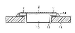
図1,図2には、実施例の放熱板を備えた電子部品の実装構造が示され、図3には、電気回路基板の構成が示され、図4には、実施例の片面樹脂モールド素子の構成が示されており、まずこの片面樹脂モールド素子10について説明する。図4に示されるように、リード(又はリードフレーム)1の下面に、樹脂フィルム(薄膜)2が貼着され、このリード1の上側にダイヤタッチ材等で回路素子(半導体素子)3が接続されており、この回路素子3の上面端子はリード1に金属のワイヤ4にて接続(ワイヤボンディング)される。なお、リード1の厚さは、統一されている。 1 and 2 show a mounting structure of an electronic component provided with the heat sink of the embodiment, FIG. 3 shows a configuration of an electric circuit board, and FIG. 4 shows a single-sided resin mold of the embodiment. The structure of the element is shown. First, the single-sided
実際の製造では、複数の回路素子3をリードフレームに接続した集合体において、上側モールド金型により片面樹脂モールドが行われることで、図示されるように、リード1の側面部(各リード間)、回路素子3の周囲、そして回路素子3とワイヤ4との接続部に樹脂5が成形される。 In actual manufacture, a single-sided resin mold is performed by an upper mold in an assembly in which a plurality of
このような片面樹脂モールド素子10を、実施例では図3の電気回路基板に接続することで、図2のような配置となる。即ち、図3のように、電気回路基板11には、片面樹脂モールド素子10を配置するための開口(又は凹部)12が設けられると共に、必要な配線パターン(電極や配線の導体パターン)13が形成される。そして、片面樹脂モールド素子10の裏面を上側にしてその樹脂モールド部を上記開口12内に挿入・配置し、配線パターン13の電極に、片面樹脂モールド素子10のリード1を半田14により接続することで、図2の状態とする。 By connecting such a single-sided
図1に示されるように、本実施例では、電気回路基板11に設けられた複数組の開口12及び配線パターン13に対し、複数の片面樹脂モールド素子10が実装されており、これら片面樹脂モールド素子10の裏面は同一水平面に並ぶ状態となる。そして、複数の片面樹脂モールド素子10の裏面に絶縁のための樹脂フィルム2を介して、放熱フィンを有する放熱板16が接着剤等で接着される。 As shown in FIG. 1, in this embodiment, a plurality of single-sided
以上の実施例によれば、複数の片面樹脂モールド素子10に対し1個の放熱板16を容易に配置することができ、放熱板を備えた電子部品を簡単に製造できる。即ち、上記リード1及び樹脂フィルム2の厚さを均一にすることで、複数の片面樹脂モールド素子10に対してもフラットな面に放熱板16を容易に配置することが可能である。半導体回路の製造では、リード(又はリードフレーム)の厚さは統一されているので、複数の片面樹脂モールド素子10の高さはほぼ同じとなる。 According to the above embodiment, one
このように本実施例では、複数の片面樹脂モールド素子10に対する放熱板16による高放熱化を良好に図ることが可能となる。なお、上記放熱板16は、複数の複数の片面樹脂モールド素子10にまたがり配置されているが、電気回路基板に実装されている全ての片面樹脂モールド素子10に対して1個の放熱板16を配置することに限定されるものではなく、複数の片面樹脂モールド素子にまたがって配置された放熱板16が、複数配置されていても良いことは言うまでもない。 As described above, in this embodiment, it is possible to favorably achieve high heat dissipation by the
更に、本実施例では、片面樹脂モールド素子を用いることで、更に効率よく放熱板16が回路素子へ取り付けられる。一般に、リード1が設けられた片面樹脂モールド素子10に対し放熱板を設ける際には、リード1と他の部品との導通(電気的接触)を防ぐために、絶縁性の接着剤等をリード1が設けられた片面樹脂モールド素子10の裏面(下面)に配置する必要がある。 Furthermore, in this embodiment, the
一方、上述のように、片面樹脂モールド素子の製造では、モールド樹脂がリードフレームの下側へ漏れないようにするため、リード(リードフレーム)を接続した回路素子全体の下面(裏面)側に樹脂フィルムが配置され、この樹脂フィルムは樹脂モールド後に剥がされる。そこで、本実施例では、この樹脂フィルム2を剥がさずそのまま用い、この樹脂フィルム2に放熱板16を直接実装することで、この樹脂フィルム2を他の部品との導通を防ぐものとして配置することができる。 On the other hand, as described above, in the manufacture of a single-sided resin mold element, in order to prevent the mold resin from leaking to the lower side of the lead frame, the resin is applied to the lower surface (back surface) side of the entire circuit element to which the lead (lead frame) is connected. A film is arranged, and this resin film is peeled off after resin molding. Therefore, in this embodiment, the
また、実施例では、開口(又は凹部)12に片面樹脂モールド素子10を配置しており、これにより、回路部品の薄型化を図ることも可能である。 In the embodiment, the single-sided
1…リード、 2…樹脂フィルム、
3…回路素子、 5…モールド樹脂、
10…片面樹脂モールド素子、
12…開口、 14…半田、
16…放熱板。1 ... lead, 2 ... resin film,
3 ... Circuit element, 5 ... Mold resin,
10: Single-sided resin mold element,
12 ... Opening, 14 ... Solder,
16 ... A heat sink.
Claims (1)
Translated fromJapanese上記リード部を電気回路基板の電極に接続すると共に、上記電子部品の樹脂モールド部を上記電気回路基板に形成された開口内又は凹部内に配置することにより、複数の上記電子部品の一方の面が同一水平面に並ぶように実装し、
上記複数の電子部品の上記一方の面上に単一の放熱板を実装する放熱板を備えた電子部品の実装構造。The lead portionis arranged on one surface, and is composed of a single-sided resin mold element in which a resin mold is formed on the opposite surface side from the one surface, andhas aplurality of electronic components in which theone surface is substantially flat,
The lead part is connected to the electrode of the electric circuit board, andthe resin mold part of the electronic component is disposed in an opening or a recess formed in the electric circuit board, thereby providing one surfaceof the plurality of electronic parts. Are mounted on the same horizontal plane,
Mounting structure of an electronic component having a heat sink to implement a single radiating plate on said one side ofsaid plurality of electronic components.
Priority Applications (2)
| Application Number | Priority Date | Filing Date | Title |
|---|---|---|---|
| JP2014107397AJP6312527B2 (en) | 2014-05-23 | 2014-05-23 | Electronic component mounting structure with heat sink |
| US14/618,284US9433076B2 (en) | 2014-05-23 | 2015-02-10 | Mounting structure of electronic components provided with heat sink |
Applications Claiming Priority (1)
| Application Number | Priority Date | Filing Date | Title |
|---|---|---|---|
| JP2014107397AJP6312527B2 (en) | 2014-05-23 | 2014-05-23 | Electronic component mounting structure with heat sink |
Publications (2)
| Publication Number | Publication Date |
|---|---|
| JP2015222795A JP2015222795A (en) | 2015-12-10 |
| JP6312527B2true JP6312527B2 (en) | 2018-04-18 |
Family
ID=54557070
Family Applications (1)
| Application Number | Title | Priority Date | Filing Date |
|---|---|---|---|
| JP2014107397AActiveJP6312527B2 (en) | 2014-05-23 | 2014-05-23 | Electronic component mounting structure with heat sink |
Country Status (2)
| Country | Link |
|---|---|
| US (1) | US9433076B2 (en) |
| JP (1) | JP6312527B2 (en) |
Families Citing this family (3)
| Publication number | Priority date | Publication date | Assignee | Title |
|---|---|---|---|---|
| FR3036918B1 (en)* | 2015-05-29 | 2018-08-10 | Thales | ELECTRONIC CARD AND METHOD OF MANUFACTURING THE SAME |
| DE102017130342A1 (en)* | 2017-12-18 | 2019-06-19 | Melexis Bulgaria Ltd. | Reinforced electronic device for an electric motor |
| JP2020107815A (en)* | 2018-12-28 | 2020-07-09 | 新日本無線株式会社 | Semiconductor device and method for manufacturing the same |
Family Cites Families (28)
| Publication number | Priority date | Publication date | Assignee | Title |
|---|---|---|---|---|
| CN1146988C (en)* | 1997-12-08 | 2004-04-21 | 东芝株式会社 | Package for semiconductor power device and method for assembling the same |
| JP2001144403A (en)* | 1999-11-11 | 2001-05-25 | Yazaki Corp | Heat dissipation mounting structure of electric component and method of mounting electric component |
| JP3830726B2 (en)* | 2000-04-26 | 2006-10-11 | 松下電器産業株式会社 | Thermally conductive substrate, manufacturing method thereof, and power module |
| US7161239B2 (en)* | 2000-12-22 | 2007-01-09 | Broadcom Corporation | Ball grid array package enhanced with a thermal and electrical connector |
| US7132744B2 (en)* | 2000-12-22 | 2006-11-07 | Broadcom Corporation | Enhanced die-up ball grid array packages and method for making the same |
| US20020079572A1 (en)* | 2000-12-22 | 2002-06-27 | Khan Reza-Ur Rahman | Enhanced die-up ball grid array and method for making the same |
| US6906414B2 (en)* | 2000-12-22 | 2005-06-14 | Broadcom Corporation | Ball grid array package with patterned stiffener layer |
| US20040217472A1 (en)* | 2001-02-16 | 2004-11-04 | Integral Technologies, Inc. | Low cost chip carrier with integrated antenna, heat sink, or EMI shielding functions manufactured from conductive loaded resin-based materials |
| JP4006189B2 (en)* | 2001-04-19 | 2007-11-14 | 株式会社ケーヒン | Control unit structure for vehicle |
| US7009291B2 (en)* | 2002-12-25 | 2006-03-07 | Denso Corporation | Semiconductor module and semiconductor device |
| JP4628687B2 (en)* | 2004-03-09 | 2011-02-09 | ルネサスエレクトロニクス株式会社 | Semiconductor device |
| US7786591B2 (en)* | 2004-09-29 | 2010-08-31 | Broadcom Corporation | Die down ball grid array package |
| JP4538359B2 (en)* | 2005-03-31 | 2010-09-08 | 株式会社日立産機システム | Electrical circuit module |
| US7582951B2 (en)* | 2005-10-20 | 2009-09-01 | Broadcom Corporation | Methods and apparatus for improved thermal performance and electromagnetic interference (EMI) shielding in leadframe integrated circuit (IC) packages |
| US8018056B2 (en)* | 2005-12-21 | 2011-09-13 | International Rectifier Corporation | Package for high power density devices |
| JP2007305702A (en)* | 2006-05-10 | 2007-11-22 | Toshiba Corp | Semiconductor device and manufacturing method thereof |
| JP2007335663A (en)* | 2006-06-15 | 2007-12-27 | Toyota Motor Corp | Semiconductor module |
| JP2008305937A (en)* | 2007-06-07 | 2008-12-18 | Panasonic Corp | Electronic component built-in module and manufacturing method thereof |
| JP5098772B2 (en)* | 2007-06-29 | 2012-12-12 | ダイキン工業株式会社 | Electrical component unit |
| US8207607B2 (en)* | 2007-12-14 | 2012-06-26 | Denso Corporation | Semiconductor device with resin mold |
| US7871862B2 (en)* | 2008-09-08 | 2011-01-18 | Stats Chippac Ltd. | Ball grid array package stacking system |
| JP2010103244A (en)* | 2008-10-22 | 2010-05-06 | Sony Corp | Semiconductor device, and method of manufacturing the same |
| JP2011171656A (en) | 2010-02-22 | 2011-09-01 | Renesas Electronics Corp | Semiconductor package and method for manufacturing the same |
| JP5062302B2 (en)* | 2010-06-29 | 2012-10-31 | 株式会社デンソー | Mounting structure of wiring board with built-in electronic components to cooler and mounting method thereof |
| WO2012164506A1 (en)* | 2011-05-31 | 2012-12-06 | Sabic Innovative Plastics Ip B.V. | Led plastic heat sink and method for making and using the same |
| JP5779042B2 (en) | 2011-08-18 | 2015-09-16 | 新光電気工業株式会社 | Semiconductor device |
| JP2013123031A (en)* | 2011-11-07 | 2013-06-20 | Denso Corp | Conductive material and semiconductor device |
| US8937384B2 (en)* | 2012-04-25 | 2015-01-20 | Qualcomm Incorporated | Thermal management of integrated circuits using phase change material and heat spreaders |
- 2014
- 2014-05-23JPJP2014107397Apatent/JP6312527B2/enactiveActive
- 2015
- 2015-02-10USUS14/618,284patent/US9433076B2/enactiveActive
Also Published As
| Publication number | Publication date |
|---|---|
| JP2015222795A (en) | 2015-12-10 |
| US9433076B2 (en) | 2016-08-30 |
| US20150342025A1 (en) | 2015-11-26 |
Similar Documents
| Publication | Publication Date | Title |
|---|---|---|
| US9966327B2 (en) | Lead frame, semiconductor device, method for manufacturing lead frame, and method for manufacturing semiconductor device | |
| JP5936310B2 (en) | Power semiconductor module and its mounting structure | |
| EP3310140B1 (en) | Mounting assembly with a heatsink | |
| JP5106519B2 (en) | Thermally conductive substrate and electronic component mounting method thereof | |
| CN106463930A (en) | Circuit structure and electric junction box | |
| JP5885630B2 (en) | Printed board | |
| KR101435451B1 (en) | metal printed circuit board and manufacturing method thereof | |
| JP2016181536A (en) | Power semiconductor device | |
| JP2008198921A (en) | Module parts and manufacturing method thereof | |
| JP6048238B2 (en) | Electronic equipment | |
| JP6312527B2 (en) | Electronic component mounting structure with heat sink | |
| JP6834815B2 (en) | Semiconductor module | |
| TWI472275B (en) | An electric circuit board using metal plates and packaging module thereof | |
| KR102362724B1 (en) | Power module and manufacturing method thereof | |
| JP5498604B1 (en) | Hollow package for solid-state image sensor | |
| JP5245880B2 (en) | Power semiconductor module and manufacturing method thereof | |
| JP6315108B2 (en) | Power semiconductor package elements | |
| WO2018123381A1 (en) | Circuit module and method for manufacturing same | |
| TW201546991A (en) | Power device | |
| JP2013008748A (en) | Semiconductor device | |
| US20170303385A1 (en) | Heat dissipating structure | |
| JP6111284B2 (en) | Hollow package manufacturing method, solid-state imaging device manufacturing method, hollow package and solid-state imaging device | |
| US10973153B2 (en) | Power module | |
| US11553616B2 (en) | Module with power device | |
| CN111146096B (en) | Double-sided heat dissipation semiconductor device and single-reflow soldering method thereof |
Legal Events
| Date | Code | Title | Description |
|---|---|---|---|
| A621 | Written request for application examination | Free format text:JAPANESE INTERMEDIATE CODE: A621 Effective date:20170303 | |
| A977 | Report on retrieval | Free format text:JAPANESE INTERMEDIATE CODE: A971007 Effective date:20171115 | |
| A131 | Notification of reasons for refusal | Free format text:JAPANESE INTERMEDIATE CODE: A131 Effective date:20171130 | |
| A521 | Request for written amendment filed | Free format text:JAPANESE INTERMEDIATE CODE: A523 Effective date:20180115 | |
| TRDD | Decision of grant or rejection written | ||
| A01 | Written decision to grant a patent or to grant a registration (utility model) | Free format text:JAPANESE INTERMEDIATE CODE: A01 Effective date:20180313 | |
| A61 | First payment of annual fees (during grant procedure) | Free format text:JAPANESE INTERMEDIATE CODE: A61 Effective date:20180320 | |
| R150 | Certificate of patent or registration of utility model | Ref document number:6312527 Country of ref document:JP Free format text:JAPANESE INTERMEDIATE CODE: R150 | |
| R250 | Receipt of annual fees | Free format text:JAPANESE INTERMEDIATE CODE: R250 | |
| R250 | Receipt of annual fees | Free format text:JAPANESE INTERMEDIATE CODE: R250 | |
| R250 | Receipt of annual fees | Free format text:JAPANESE INTERMEDIATE CODE: R250 | |
| R250 | Receipt of annual fees | Free format text:JAPANESE INTERMEDIATE CODE: R250 | |
| R250 | Receipt of annual fees | Free format text:JAPANESE INTERMEDIATE CODE: R250 |