JP6286941B2 - LIGHT EMITTING DEVICE, LIGHT EMITTING DEVICE MANUFACTURING METHOD, ELECTRONIC DEVICE - Google Patents
LIGHT EMITTING DEVICE, LIGHT EMITTING DEVICE MANUFACTURING METHOD, ELECTRONIC DEVICEDownload PDFInfo
- Publication number
- JP6286941B2 JP6286941B2JP2013175339AJP2013175339AJP6286941B2JP 6286941 B2JP6286941 B2JP 6286941B2JP 2013175339 AJP2013175339 AJP 2013175339AJP 2013175339 AJP2013175339 AJP 2013175339AJP 6286941 B2JP6286941 B2JP 6286941B2
- Authority
- JP
- Japan
- Prior art keywords
- layer
- insulating film
- light emitting
- pixel electrode
- layer thickness
- Prior art date
- Legal status (The legal status is an assumption and is not a legal conclusion. Google has not performed a legal analysis and makes no representation as to the accuracy of the status listed.)
- Active
Links
- 238000004519manufacturing processMethods0.000titleclaimsdescription20
- 239000010410layerSubstances0.000claimsdescription500
- 238000000034methodMethods0.000claimsdescription51
- 239000002346layers by functionSubstances0.000claimsdescription49
- 239000000463materialSubstances0.000claimsdescription16
- 239000011347resinSubstances0.000claimsdescription12
- 229920005989resinPolymers0.000claimsdescription12
- 230000000149penetrating effectEffects0.000claimsdescription10
- 230000002093peripheral effectEffects0.000claimsdescription8
- 238000001579optical reflectometryMethods0.000claimsdescription5
- 230000005540biological transmissionEffects0.000claims1
- 239000010408filmSubstances0.000description445
- 230000003287optical effectEffects0.000description53
- 239000011229interlayerSubstances0.000description44
- 239000000758substrateSubstances0.000description36
- 238000007789sealingMethods0.000description35
- 230000008569processEffects0.000description22
- 238000005530etchingMethods0.000description21
- 239000003990capacitorSubstances0.000description19
- 238000003860storageMethods0.000description19
- VYPSYNLAJGMNEJ-UHFFFAOYSA-NSilicium dioxideChemical compoundO=[Si]=OVYPSYNLAJGMNEJ-UHFFFAOYSA-N0.000description16
- 230000004048modificationEffects0.000description15
- 238000012986modificationMethods0.000description15
- 229910052814silicon oxideInorganic materials0.000description14
- 239000004925Acrylic resinSubstances0.000description9
- 229920000178Acrylic resinPolymers0.000description9
- 229910052581Si3N4Inorganic materials0.000description9
- 238000000059patterningMethods0.000description9
- HQVNEWCFYHHQES-UHFFFAOYSA-Nsilicon nitrideChemical compoundN12[Si]34N5[Si]62N3[Si]51N64HQVNEWCFYHHQES-UHFFFAOYSA-N0.000description9
- 238000005468ion implantationMethods0.000description8
- 150000002500ionsChemical class0.000description6
- 238000005268plasma chemical vapour depositionMethods0.000description6
- 239000011368organic materialSubstances0.000description5
- 239000004065semiconductorSubstances0.000description5
- XUIMIQQOPSSXEZ-UHFFFAOYSA-NSiliconChemical compound[Si]XUIMIQQOPSSXEZ-UHFFFAOYSA-N0.000description4
- 239000011159matrix materialSubstances0.000description4
- 238000005192partitionMethods0.000description4
- 238000000206photolithographyMethods0.000description4
- 229910052710siliconInorganic materials0.000description4
- 239000010703siliconSubstances0.000description4
- 239000010409thin filmSubstances0.000description4
- QVGXLLKOCUKJST-UHFFFAOYSA-Natomic oxygenChemical compound[O]QVGXLLKOCUKJST-UHFFFAOYSA-N0.000description3
- 230000008859changeEffects0.000description3
- 239000003086colorantSubstances0.000description3
- 239000000470constituentSubstances0.000description3
- 238000010586diagramMethods0.000description3
- 239000011521glassSubstances0.000description3
- 239000001301oxygenSubstances0.000description3
- 229910052760oxygenInorganic materials0.000description3
- 239000004417polycarbonateSubstances0.000description3
- 229920000515polycarbonatePolymers0.000description3
- 238000004544sputter depositionMethods0.000description3
- 229910000838Al alloyInorganic materials0.000description2
- YCKRFDGAMUMZLT-UHFFFAOYSA-NFluorine atomChemical compound[F]YCKRFDGAMUMZLT-UHFFFAOYSA-N0.000description2
- 239000004642PolyimideSubstances0.000description2
- NRTOMJZYCJJWKI-UHFFFAOYSA-NTitanium nitrideChemical compound[Ti]#NNRTOMJZYCJJWKI-UHFFFAOYSA-N0.000description2
- -1acryloyl compoundChemical class0.000description2
- 125000002723alicyclic groupChemical group0.000description2
- 229910045601alloyInorganic materials0.000description2
- 239000000956alloySubstances0.000description2
- 229910052782aluminiumInorganic materials0.000description2
- XAGFODPZIPBFFR-UHFFFAOYSA-NaluminiumChemical compound[Al]XAGFODPZIPBFFR-UHFFFAOYSA-N0.000description2
- 230000004888barrier functionEffects0.000description2
- 239000004020conductorSubstances0.000description2
- 238000001312dry etchingMethods0.000description2
- 239000003822epoxy resinSubstances0.000description2
- NIHNNTQXNPWCJQ-UHFFFAOYSA-NfluoreneChemical compoundC1=CC=C2CC3=CC=CC=C3C2=C1NIHNNTQXNPWCJQ-UHFFFAOYSA-N0.000description2
- 229910052731fluorineInorganic materials0.000description2
- 239000011737fluorineSubstances0.000description2
- 239000007789gasSubstances0.000description2
- 238000010438heat treatmentMethods0.000description2
- 229910010272inorganic materialInorganic materials0.000description2
- 239000011147inorganic materialSubstances0.000description2
- 230000010363phase shiftEffects0.000description2
- 229920002120photoresistant polymerPolymers0.000description2
- 229910021420polycrystalline siliconInorganic materials0.000description2
- 229920000647polyepoxidePolymers0.000description2
- 229920000728polyesterPolymers0.000description2
- 229920001721polyimidePolymers0.000description2
- 229920005591polysiliconPolymers0.000description2
- 239000010453quartzSubstances0.000description2
- 229910052709silverInorganic materials0.000description2
- 238000002834transmittanceMethods0.000description2
- ODIGIKRIUKFKHP-UHFFFAOYSA-N(n-propan-2-yloxycarbonylanilino) acetateChemical compoundCC(C)OC(=O)N(OC(C)=O)C1=CC=CC=C1ODIGIKRIUKFKHP-UHFFFAOYSA-N0.000description1
- 229930192627NaphthoquinoneNatural products0.000description1
- 239000004696Poly ether ether ketoneSubstances0.000description1
- 239000004952PolyamideSubstances0.000description1
- 239000004962Polyamide-imideSubstances0.000description1
- 239000004695Polyether sulfoneSubstances0.000description1
- 239000004697PolyetherimideSubstances0.000description1
- 239000004793PolystyreneSubstances0.000description1
- GWEVSGVZZGPLCZ-UHFFFAOYSA-NTitan oxideChemical compoundO=[Ti]=OGWEVSGVZZGPLCZ-UHFFFAOYSA-N0.000description1
- NIXOWILDQLNWCW-UHFFFAOYSA-Nacrylic acid groupChemical groupC(C=C)(=O)ONIXOWILDQLNWCW-UHFFFAOYSA-N0.000description1
- 230000002411adverseEffects0.000description1
- 230000008901benefitEffects0.000description1
- 230000015572biosynthetic processEffects0.000description1
- 230000000903blocking effectEffects0.000description1
- 229920002678cellulosePolymers0.000description1
- 239000001913celluloseSubstances0.000description1
- 239000000919ceramicSubstances0.000description1
- 238000005229chemical vapour depositionMethods0.000description1
- 239000011248coating agentSubstances0.000description1
- 238000000576coating methodMethods0.000description1
- 150000001875compoundsChemical class0.000description1
- 229920001577copolymerPolymers0.000description1
- 230000007547defectEffects0.000description1
- 238000000151depositionMethods0.000description1
- 230000006866deteriorationEffects0.000description1
- 230000000694effectsEffects0.000description1
- 238000005401electroluminescenceMethods0.000description1
- 230000005669field effectEffects0.000description1
- 125000003983fluorenyl groupChemical groupC1(=CC=CC=2C3=CC=CC=C3CC12)*0.000description1
- 230000005525hole transportEffects0.000description1
- 238000005286illuminationMethods0.000description1
- AMGQUBHHOARCQH-UHFFFAOYSA-Nindium;oxotinChemical compound[In].[Sn]=OAMGQUBHHOARCQH-UHFFFAOYSA-N0.000description1
- 238000002347injectionMethods0.000description1
- 239000007924injectionSubstances0.000description1
- 239000011810insulating materialSubstances0.000description1
- 230000007257malfunctionEffects0.000description1
- 229910044991metal oxideInorganic materials0.000description1
- 150000004706metal oxidesChemical class0.000description1
- 239000000113methacrylic resinSubstances0.000description1
- 150000002791naphthoquinonesChemical class0.000description1
- 231100000989no adverse effectToxicity0.000description1
- 229920003986novolacPolymers0.000description1
- 150000003961organosilicon compoundsChemical class0.000description1
- 238000002161passivationMethods0.000description1
- 238000002294plasma sputter depositionMethods0.000description1
- 229920002492poly(sulfone)Polymers0.000description1
- 229920002647polyamidePolymers0.000description1
- 229920002312polyamide-imidePolymers0.000description1
- 229920001230polyarylatePolymers0.000description1
- 229920006393polyether sulfonePolymers0.000description1
- 229920002530polyetherether ketonePolymers0.000description1
- 229920001601polyetherimidePolymers0.000description1
- 229920000098polyolefinPolymers0.000description1
- 229920001296polysiloxanePolymers0.000description1
- 229920002223polystyrenePolymers0.000description1
- 239000004814polyurethaneSubstances0.000description1
- 229920002635polyurethanePolymers0.000description1
- 230000009467reductionEffects0.000description1
- 239000002356single layerSubstances0.000description1
- OGIDPMRJRNCKJF-UHFFFAOYSA-Ntitanium oxideInorganic materials[Ti]=OOGIDPMRJRNCKJF-UHFFFAOYSA-N0.000description1
Images


Classifications
- H—ELECTRICITY
- H10—SEMICONDUCTOR DEVICES; ELECTRIC SOLID-STATE DEVICES NOT OTHERWISE PROVIDED FOR
- H10K—ORGANIC ELECTRIC SOLID-STATE DEVICES
- H10K59/00—Integrated devices, or assemblies of multiple devices, comprising at least one organic light-emitting element covered by group H10K50/00
- H10K59/30—Devices specially adapted for multicolour light emission
- H10K59/35—Devices specially adapted for multicolour light emission comprising red-green-blue [RGB] subpixels
- H—ELECTRICITY
- H10—SEMICONDUCTOR DEVICES; ELECTRIC SOLID-STATE DEVICES NOT OTHERWISE PROVIDED FOR
- H10K—ORGANIC ELECTRIC SOLID-STATE DEVICES
- H10K50/00—Organic light-emitting devices
- H10K50/80—Constructional details
- H10K50/85—Arrangements for extracting light from the devices
- H10K50/852—Arrangements for extracting light from the devices comprising a resonant cavity structure, e.g. Bragg reflector pair
- H—ELECTRICITY
- H10—SEMICONDUCTOR DEVICES; ELECTRIC SOLID-STATE DEVICES NOT OTHERWISE PROVIDED FOR
- H10K—ORGANIC ELECTRIC SOLID-STATE DEVICES
- H10K50/00—Organic light-emitting devices
- H10K50/80—Constructional details
- H10K50/85—Arrangements for extracting light from the devices
- H10K50/856—Arrangements for extracting light from the devices comprising reflective means
- H—ELECTRICITY
- H10—SEMICONDUCTOR DEVICES; ELECTRIC SOLID-STATE DEVICES NOT OTHERWISE PROVIDED FOR
- H10K—ORGANIC ELECTRIC SOLID-STATE DEVICES
- H10K59/00—Integrated devices, or assemblies of multiple devices, comprising at least one organic light-emitting element covered by group H10K50/00
- H10K59/10—OLED displays
- H10K59/12—Active-matrix OLED [AMOLED] displays
- H10K59/121—Active-matrix OLED [AMOLED] displays characterised by the geometry or disposition of pixel elements
- H10K59/1213—Active-matrix OLED [AMOLED] displays characterised by the geometry or disposition of pixel elements the pixel elements being TFTs
- H—ELECTRICITY
- H10—SEMICONDUCTOR DEVICES; ELECTRIC SOLID-STATE DEVICES NOT OTHERWISE PROVIDED FOR
- H10K—ORGANIC ELECTRIC SOLID-STATE DEVICES
- H10K59/00—Integrated devices, or assemblies of multiple devices, comprising at least one organic light-emitting element covered by group H10K50/00
- H10K59/10—OLED displays
- H10K59/12—Active-matrix OLED [AMOLED] displays
- H10K59/123—Connection of the pixel electrodes to the thin film transistors [TFT]
- H—ELECTRICITY
- H10—SEMICONDUCTOR DEVICES; ELECTRIC SOLID-STATE DEVICES NOT OTHERWISE PROVIDED FOR
- H10K—ORGANIC ELECTRIC SOLID-STATE DEVICES
- H10K59/00—Integrated devices, or assemblies of multiple devices, comprising at least one organic light-emitting element covered by group H10K50/00
- H10K59/10—OLED displays
- H10K59/12—Active-matrix OLED [AMOLED] displays
- H10K59/124—Insulating layers formed between TFT elements and OLED elements
- H—ELECTRICITY
- H10—SEMICONDUCTOR DEVICES; ELECTRIC SOLID-STATE DEVICES NOT OTHERWISE PROVIDED FOR
- H10K—ORGANIC ELECTRIC SOLID-STATE DEVICES
- H10K59/00—Integrated devices, or assemblies of multiple devices, comprising at least one organic light-emitting element covered by group H10K50/00
- H10K59/10—OLED displays
- H10K59/12—Active-matrix OLED [AMOLED] displays
- H10K59/126—Shielding, e.g. light-blocking means over the TFTs
- H—ELECTRICITY
- H10—SEMICONDUCTOR DEVICES; ELECTRIC SOLID-STATE DEVICES NOT OTHERWISE PROVIDED FOR
- H10K—ORGANIC ELECTRIC SOLID-STATE DEVICES
- H10K59/00—Integrated devices, or assemblies of multiple devices, comprising at least one organic light-emitting element covered by group H10K50/00
- H10K59/30—Devices specially adapted for multicolour light emission
- H10K59/38—Devices specially adapted for multicolour light emission comprising colour filters or colour changing media [CCM]
- H—ELECTRICITY
- H10—SEMICONDUCTOR DEVICES; ELECTRIC SOLID-STATE DEVICES NOT OTHERWISE PROVIDED FOR
- H10K—ORGANIC ELECTRIC SOLID-STATE DEVICES
- H10K59/00—Integrated devices, or assemblies of multiple devices, comprising at least one organic light-emitting element covered by group H10K50/00
- H10K59/80—Constructional details
- H10K59/805—Electrodes
- H10K59/8051—Anodes
- H10K59/80518—Reflective anodes, e.g. ITO combined with thick metallic layers
- H—ELECTRICITY
- H10—SEMICONDUCTOR DEVICES; ELECTRIC SOLID-STATE DEVICES NOT OTHERWISE PROVIDED FOR
- H10K—ORGANIC ELECTRIC SOLID-STATE DEVICES
- H10K59/00—Integrated devices, or assemblies of multiple devices, comprising at least one organic light-emitting element covered by group H10K50/00
- H10K59/80—Constructional details
- H10K59/875—Arrangements for extracting light from the devices
- H10K59/876—Arrangements for extracting light from the devices comprising a resonant cavity structure, e.g. Bragg reflector pair
- H—ELECTRICITY
- H10—SEMICONDUCTOR DEVICES; ELECTRIC SOLID-STATE DEVICES NOT OTHERWISE PROVIDED FOR
- H10K—ORGANIC ELECTRIC SOLID-STATE DEVICES
- H10K59/00—Integrated devices, or assemblies of multiple devices, comprising at least one organic light-emitting element covered by group H10K50/00
- H10K59/80—Constructional details
- H10K59/875—Arrangements for extracting light from the devices
- H10K59/878—Arrangements for extracting light from the devices comprising reflective means
- H—ELECTRICITY
- H10—SEMICONDUCTOR DEVICES; ELECTRIC SOLID-STATE DEVICES NOT OTHERWISE PROVIDED FOR
- H10K—ORGANIC ELECTRIC SOLID-STATE DEVICES
- H10K2102/00—Constructional details relating to the organic devices covered by this subclass
- H10K2102/301—Details of OLEDs
- H10K2102/302—Details of OLEDs of OLED structures
- H10K2102/3023—Direction of light emission
- H10K2102/3026—Top emission
- H—ELECTRICITY
- H10—SEMICONDUCTOR DEVICES; ELECTRIC SOLID-STATE DEVICES NOT OTHERWISE PROVIDED FOR
- H10K—ORGANIC ELECTRIC SOLID-STATE DEVICES
- H10K2102/00—Constructional details relating to the organic devices covered by this subclass
- H10K2102/301—Details of OLEDs
- H10K2102/341—Short-circuit prevention
- H—ELECTRICITY
- H10—SEMICONDUCTOR DEVICES; ELECTRIC SOLID-STATE DEVICES NOT OTHERWISE PROVIDED FOR
- H10K—ORGANIC ELECTRIC SOLID-STATE DEVICES
- H10K50/00—Organic light-emitting devices
- H—ELECTRICITY
- H10—SEMICONDUCTOR DEVICES; ELECTRIC SOLID-STATE DEVICES NOT OTHERWISE PROVIDED FOR
- H10K—ORGANIC ELECTRIC SOLID-STATE DEVICES
- H10K50/00—Organic light-emitting devices
- H10K50/80—Constructional details
- H10K50/805—Electrodes
- H—ELECTRICITY
- H10—SEMICONDUCTOR DEVICES; ELECTRIC SOLID-STATE DEVICES NOT OTHERWISE PROVIDED FOR
- H10K—ORGANIC ELECTRIC SOLID-STATE DEVICES
- H10K50/00—Organic light-emitting devices
- H10K50/80—Constructional details
- H10K50/805—Electrodes
- H10K50/81—Anodes
- H10K50/818—Reflective anodes, e.g. ITO combined with thick metallic layers
- H—ELECTRICITY
- H10—SEMICONDUCTOR DEVICES; ELECTRIC SOLID-STATE DEVICES NOT OTHERWISE PROVIDED FOR
- H10K—ORGANIC ELECTRIC SOLID-STATE DEVICES
- H10K50/00—Organic light-emitting devices
- H10K50/80—Constructional details
- H10K50/805—Electrodes
- H10K50/82—Cathodes
- H10K50/824—Cathodes combined with auxiliary electrodes
- H—ELECTRICITY
- H10—SEMICONDUCTOR DEVICES; ELECTRIC SOLID-STATE DEVICES NOT OTHERWISE PROVIDED FOR
- H10K—ORGANIC ELECTRIC SOLID-STATE DEVICES
- H10K59/00—Integrated devices, or assemblies of multiple devices, comprising at least one organic light-emitting element covered by group H10K50/00
- H10K59/10—OLED displays
- H10K59/12—Active-matrix OLED [AMOLED] displays
- H10K59/1201—Manufacture or treatment
- H—ELECTRICITY
- H10—SEMICONDUCTOR DEVICES; ELECTRIC SOLID-STATE DEVICES NOT OTHERWISE PROVIDED FOR
- H10K—ORGANIC ELECTRIC SOLID-STATE DEVICES
- H10K59/00—Integrated devices, or assemblies of multiple devices, comprising at least one organic light-emitting element covered by group H10K50/00
- H10K59/30—Devices specially adapted for multicolour light emission
- H10K59/35—Devices specially adapted for multicolour light emission comprising red-green-blue [RGB] subpixels
- H10K59/351—Devices specially adapted for multicolour light emission comprising red-green-blue [RGB] subpixels comprising more than three subpixels, e.g. red-green-blue-white [RGBW]
Landscapes
- Engineering & Computer Science (AREA)
- Microelectronics & Electronic Packaging (AREA)
- Physics & Mathematics (AREA)
- Optics & Photonics (AREA)
- Geometry (AREA)
- Manufacturing & Machinery (AREA)
- Electroluminescent Light Sources (AREA)
- Devices For Indicating Variable Information By Combining Individual Elements (AREA)
Description
Translated fromJapanese本発明は、発光装置、発光装置の製造方法、及び当該発光装置を搭載した電子機器に関する。 The present invention relates to a light emitting device, a method for manufacturing the light emitting device, and an electronic apparatus equipped with the light emitting device.
発光装置の一例として、例えば有機エレクトロルミネッセンス(以降、有機ELと称す)素子がマトリックス状に配置された電気光学装置(特許文献1)が提案されている。特許文献1に記載の電気光学装置は、薄膜トランジスターを有し、光を発する画素がマトリックス状に配置されたアクティブマトリックス型の発光装置である。画素には、光反射層と、透光性絶縁膜と、第1電極(画素電極)と、隔壁層と、発光機能層と、第2電極(対向電極)とが順に積層されている。 As an example of a light emitting device, for example, an electro-optical device (Patent Document 1) in which organic electroluminescence (hereinafter referred to as organic EL) elements are arranged in a matrix has been proposed. The electro-optical device described in Patent Document 1 is an active matrix light-emitting device that includes a thin film transistor and in which pixels that emit light are arranged in a matrix. In the pixel, a light reflection layer, a translucent insulating film, a first electrode (pixel electrode), a partition layer, a light emitting functional layer, and a second electrode (counter electrode) are sequentially stacked.
隔壁層で覆われていない領域の画素電極から発光機能層に電流が供給されて、発光機能層が発光する。つまり、隔壁層で覆われていない領域(隔壁層が形成されていない領域)が、発光領域となる。さらに、画素電極はコンタクトホールを覆うように設けられ、コンタクトホールを介して画素電極と薄膜トランジスターとが電気的に接続される。つまり画素電極と薄膜トランジスターとが電気的に接続される部分が、コンタクト領域となる。画素電極は、発光領域及びコンタクト領域に跨って設けられている。
透光性絶縁膜は、光反射層と対向電極との間の光学的な距離を調整する役割を有し、透光性絶縁膜の膜厚は、第1画素の発光領域>第2画素の発光領域>第3画素の発光領域>コンタクトホールの形成領域(コンタクト領域)という関係を満たすように、設定されている。A current is supplied to the light emitting functional layer from the pixel electrode in a region not covered with the partition layer, and the light emitting functional layer emits light. That is, a region not covered with the partition layer (a region where the partition layer is not formed) is a light emitting region. Further, the pixel electrode is provided so as to cover the contact hole, and the pixel electrode and the thin film transistor are electrically connected through the contact hole. That is, a portion where the pixel electrode and the thin film transistor are electrically connected becomes a contact region. The pixel electrode is provided across the light emitting region and the contact region.
The translucent insulating film has a role of adjusting the optical distance between the light reflecting layer and the counter electrode, and the thickness of the translucent insulating film is such that the light emitting region of the first pixel> the second pixel. It is set so as to satisfy the relationship of light emitting region> light emitting region of the third pixel> contact hole forming region (contact region).
かかる構成(光共振構造)によって、発光機能層で発した光は、光反射層と対向電極との間を往復し、光反射層と対向電極との間の光学的な距離、つまり透光性絶縁膜の膜厚に応じた共振波長の光が選択的に増幅され、各画素から射出される。特許文献1に記載の電気光学装置は、上記光共振構造によって、例えば、ピーク波長が610nmの赤の波長域の光、ピーク波長が540nmの緑の波長域の光、及びピーク波長が470nmの青の波長域の光、つまり色純度の高い光が各画素から表示光として射出され、優れた色再現性を有する。 With this configuration (optical resonance structure), light emitted from the light emitting functional layer reciprocates between the light reflecting layer and the counter electrode, and the optical distance between the light reflecting layer and the counter electrode, that is, translucency Light having a resonance wavelength corresponding to the thickness of the insulating film is selectively amplified and emitted from each pixel. The electro-optical device described in Patent Document 1 uses, for example, the light in the red wavelength range with a peak wavelength of 610 nm, the light in the green wavelength range with a peak wavelength of 540 nm, and the blue wavelength with a peak wavelength of 470 nm. In this wavelength range, that is, light with high color purity is emitted from each pixel as display light, and has excellent color reproducibility.
上述したように、特許文献1に記載の電気光学装置では、発光領域の透光性絶縁膜の膜厚>コンタクト領域の透光性絶縁膜の膜厚という関係を有しているので、発光領域とコンタクト領域との間に、光学的な距離が異なる境界(透光性絶縁膜の膜厚が異なる境界)が形成される。 As described above, the electro-optical device described in Patent Document 1 has the relationship that the film thickness of the light-transmitting insulating film in the light-emitting region> the film thickness of the light-transmitting insulating film in the contact region. A boundary having a different optical distance (a boundary having a different film thickness of the light-transmitting insulating film) is formed between the contact region and the contact region.
特許文献1に記載の電気光学装置では、より明るい表示を得るために発光領域を広くしようとすると、当該境界が障害となって発光領域を広くすることが難しいという課題があった。
詳しくは、当該境界を越えて発光領域を広くすると、発光領域には、光学的な距離が異なる部分が生じる。光学的な距離が異なると共振波長が変化するので、発光領域から異なる共振波長の光が発せられることになり、発光領域から発する光の色純度が低下する。このため、当該境界を越えて発光領域を広くすることが難しいという課題があった。In the electro-optical device described in Patent Document 1, when an attempt is made to widen the light emitting region in order to obtain a brighter display, there is a problem that it is difficult to widen the light emitting region because the boundary becomes an obstacle.
Specifically, when the light emitting region is widened beyond the boundary, portions having different optical distances are generated in the light emitting region. Since the resonance wavelength changes when the optical distance is different, light having a different resonance wavelength is emitted from the light emitting region, and the color purity of the light emitted from the light emitting region is lowered. For this reason, there is a problem that it is difficult to widen the light emitting region beyond the boundary.
本発明は、上述の課題の少なくとも一部を解決するためになされたものであり、以下の形態または適用例として実現することが可能である。 SUMMARY An advantage of some aspects of the invention is to solve at least a part of the problems described above, and the invention can be implemented as the following forms or application examples.
[適用例1]本適用例に係る発光装置は、トランジスターと、前記トランジスターの上方に設けられた光反射層と、前記光反射層を覆い、第1の層厚の部分と前記第1の層厚の部分よりも厚い第2の層厚の部分と前記第2の層厚の部分よりも厚い第3の層厚の部分とを有する第1の絶縁層と、前記第1の絶縁層の上に設けられた光の透過性を有する画素電極と、前記画素電極の周縁部を覆う第2の絶縁層と、前記画素電極及び前記第2の絶縁層を覆う発光機能層と、前記発光機能層を覆い光の反射性と光の透過性とを有する対向電極と、前記第1の層厚の部分の上に設けられ、少なくとも一部が前記画素電極と平面的に重なる導電層と、を含み、前記画素電極は、前記第1の層厚の部分に設けられた第1の画素電極と、前記第2の層厚の部分に設けられた第2の画素電極と、前記第3の層厚の部分に設けられた第3の画素電極と、を有し、前記第1の画素電極と、前記第2の画素電極と、前記第3の画素電極とは、前記導電層を介して前記トランジスターに接続されていることを特徴とする。 Application Example 1 A light-emitting device according to this application example includes a transistor, a light reflection layer provided above the transistor, the light reflection layer, a first layer thickness portion, and the first layer. A first insulating layer having a second layer thickness portion thicker than the thick portion and a third layer thickness portion thicker than the second layer thickness; and over the first insulating layer. A light-transmitting pixel electrode, a second insulating layer covering a peripheral portion of the pixel electrode, a light-emitting functional layer covering the pixel electrode and the second insulating layer, and the light-emitting functional layer A counter electrode having a light reflecting property and a light transmitting property, and a conductive layer provided on the first layer thickness portion and at least partially overlapping the pixel electrode in a plane. The pixel electrode includes a first pixel electrode provided in the first layer thickness portion and a second layer thickness portion. A second pixel electrode provided; and a third pixel electrode provided in a portion having the third layer thickness; the first pixel electrode; the second pixel electrode; The third pixel electrode is connected to the transistor through the conductive layer.
導電層は、第1の層厚の部分の上に設けられ、トランジスターからの信号は、導電層を介して画素電極に供給される。導電層は画素電極と平面的に重なり、導電層が設けられた領域が、トランジスターと画素電極とを接続するコンタクト領域になる。画素電極の周縁部は第2の絶縁層で覆われ、トランジスターからの信号に応じて、第2の絶縁層で覆われていない領域の画素電極から発光機能層に電流が供給され、発光機能層が発光する。つまり、第2の絶縁層で覆われていない領域が、発光機能層が発光する発光領域となる。画素電極は、コンタクト領域及び発光領域に跨って設けられている。 The conductive layer is provided on the first layer thickness portion, and a signal from the transistor is supplied to the pixel electrode through the conductive layer. The conductive layer overlaps the pixel electrode in a plan view, and a region where the conductive layer is provided becomes a contact region that connects the transistor and the pixel electrode. The peripheral edge portion of the pixel electrode is covered with the second insulating layer, and current is supplied to the light emitting functional layer from the pixel electrode in the region not covered with the second insulating layer in accordance with a signal from the transistor. Emits light. That is, a region that is not covered with the second insulating layer is a light emitting region where the light emitting functional layer emits light. The pixel electrode is provided across the contact region and the light emitting region.
発光機能層(発光領域)で発した光は、光反射層と対向電極との間を往復し、光反射層と対向電極との間の光学的な距離に応じて共振し、特定波長の光が増幅される。光学的な距離は、第1の絶縁層の層厚によって変化する。第1の絶縁層は3種類の層厚を有しているので、3種類の共振波長の光が発せられる。例えば、青、緑、赤の3種類の波長の光が増幅されるように、第1の絶縁層の層厚を調整することで、発光領域で発した青、緑、赤の光の色純度を高めることができる。 Light emitted from the light emitting functional layer (light emitting region) reciprocates between the light reflecting layer and the counter electrode, resonates according to the optical distance between the light reflecting layer and the counter electrode, and emits light of a specific wavelength. Is amplified. The optical distance varies depending on the thickness of the first insulating layer. Since the first insulating layer has three types of layer thicknesses, light having three types of resonance wavelengths is emitted. For example, the color purity of blue, green, and red light emitted in the light emitting region is adjusted by adjusting the thickness of the first insulating layer so that light of three wavelengths of blue, green, and red is amplified. Can be increased.
第1の層厚の部分に第1の画素電極が設けられ、第2の層厚の部分に第2の画素電極が設けられ、第3の層厚の部分に第3の画素電極が設けられており、それぞれの画素電極が設けられた領域の第1の絶縁層の層厚は一定である。すなわち、画素電極が設けられた領域の光学的な距離は一定になっている。 The first pixel electrode is provided in the first layer thickness portion, the second pixel electrode is provided in the second layer thickness portion, and the third pixel electrode is provided in the third layer thickness portion. The thickness of the first insulating layer in the region where each pixel electrode is provided is constant. That is, the optical distance of the region where the pixel electrode is provided is constant.
画素電極が設けられた領域の光学的な距離は一定であるので、画素電極における発光領域とコンタクト領域との間隔を小さくし、画素電極における発光領域を広くしても、光学的な距離は変化することがない。換言すれば、公知技術(特開2009−134067号公報)では画素電極が設けられた領域は光学的な距離が異なる境界を有していたが、本発明では画素電極が設けられた領域における光学的な距離は一定であるので、画素電極における発光領域を広くしても、共振波長の変化(色純度の低下)は発生せず、公知技術と比べて発光領域を広くすることができる。よって、発光領域で発する光の色純度の低下を招くことなく、発光領域で発する光の光度を高めることができる。従って、本適用例に係る発光装置では、色純度及び光度が高い表示、すなわち明るく鮮やかな色の表示を提供することができる。 Since the optical distance of the area where the pixel electrode is provided is constant, the optical distance changes even if the distance between the light emitting area and the contact area in the pixel electrode is reduced and the light emitting area in the pixel electrode is widened. There is nothing to do. In other words, in the known technique (Japanese Patent Application Laid-Open No. 2009-134067), the region where the pixel electrode is provided has a boundary with different optical distances, but in the present invention, the optical region in the region where the pixel electrode is provided. Therefore, even if the light emitting region in the pixel electrode is widened, the resonance wavelength does not change (decrease in color purity), and the light emitting region can be widened as compared with the known technique. Therefore, the luminous intensity of the light emitted from the light emitting region can be increased without causing a decrease in the color purity of the light emitted from the light emitting region. Therefore, the light emitting device according to this application example can provide a display with high color purity and luminous intensity, that is, a bright and vivid color display.
[適用例2]上記適用例に記載の発光装置において、前記第1の絶縁層は、前記反射層の側から順に積層された第1絶縁膜と第2絶縁膜と第3絶縁膜とを有し、前記第1絶縁膜は、前記第1の層厚を有し、前記第1絶縁膜と前記第2絶縁膜とが積層された部分は、前記第2の層厚を有し、前記第1絶縁膜と前記第2絶縁膜と前記第3絶縁膜とが積層された部分は、前記第3の層厚を有し、前記導電層は、第1の導電層と第2の導電層と第3の導電層とを有し、前記第1の画素電極は、前記第1の導電層に直接接し、前記第2の画素電極は、前記第2絶縁膜を貫く第1のコンタクトホールを介して前記第2の導電層に接続され、前記第3の画素電極は、前記第2絶縁膜及び前記第3絶縁膜を貫く第2のコンタクトホールを介して、前記第3の導電層に接続されていることが好ましい。 Application Example 2 In the light emitting device according to the application example described above, the first insulating layer includes a first insulating film, a second insulating film, and a third insulating film that are sequentially stacked from the reflective layer side. The first insulating film has the first layer thickness, and the portion where the first insulating film and the second insulating film are stacked has the second layer thickness, A portion where one insulating film, the second insulating film, and the third insulating film are stacked has the third layer thickness, and the conductive layer includes the first conductive layer, the second conductive layer, and the second conductive layer. A third conductive layer, wherein the first pixel electrode is in direct contact with the first conductive layer, and the second pixel electrode is interposed through a first contact hole that penetrates the second insulating film. The third pixel electrode is connected to the second conductive layer, and the third pixel electrode is connected to the third conductive layer through the second insulating film and the second contact hole that penetrates the third insulating film. It is preferably connected to the layer.
第1の層厚の部分は第1絶縁膜で構成され、第2の層厚の部分は第1絶縁膜と第2絶縁膜とで構成され、第3の層厚の部分は第1絶縁膜と第2絶縁膜と第3絶縁膜とで構成されている。第1絶縁膜、第2絶縁膜、及び第3絶縁膜が均一な膜厚を有するように制御することで、第1の層厚の部分の膜厚、第2の層厚の部分の膜厚、及び第3の層厚の部分の膜厚の均一性を高めることができる。よって、第1の画素電極が設けられた領域の光学的な距離、第2の画素電極が設けられた領域の光学的な距離、及び第3の画素電極が設けられた領域の光学的な距離の均一性を高め、各画素電極から発せられる光の共振波長のバラツキを小さくし、各画素電極の発光領域から発せられる光の色純度を高めることができる。 The first layer thickness portion is composed of the first insulating film, the second layer thickness portion is composed of the first insulating film and the second insulating film, and the third layer thickness portion is the first insulating film. And a second insulating film and a third insulating film. By controlling the first insulating film, the second insulating film, and the third insulating film to have a uniform film thickness, the film thickness of the first layer thickness portion and the film thickness of the second layer thickness portion are controlled. And the uniformity of the film thickness of the third layer thickness portion can be improved. Therefore, the optical distance of the region where the first pixel electrode is provided, the optical distance of the region where the second pixel electrode is provided, and the optical distance of the region where the third pixel electrode is provided And the variation in the resonance wavelength of the light emitted from each pixel electrode can be reduced, and the color purity of the light emitted from the light emitting region of each pixel electrode can be increased.
[適用例3]上記適用例に記載の発光装置において、前記第1の画素電極は前記第1の層厚の部分の中に設けられ、前記第2の画素電極は前記第2の層厚の部分の中に設けられていることが好ましい。 Application Example 3 In the light-emitting device according to the application example, the first pixel electrode is provided in the first layer thickness portion, and the second pixel electrode has the second layer thickness. It is preferably provided in the part.
第1の層厚の部分の中に第1の画素電極を配置することで、第1の層厚の部分に対応した共振波長の光を第1の画素電極の発光領域から発することができる。第2の層厚の部分の中に第2の画素電極を配置することで、第2の層厚の部分に対応した共振波長の光を第2の画素電極の発光領域から発することができる。よって、第1の画素電極及び第2の画素電極の発光領域から発する光の色純度を高めることができる。 By disposing the first pixel electrode in the first layer thickness portion, light having a resonance wavelength corresponding to the first layer thickness portion can be emitted from the light emitting region of the first pixel electrode. By disposing the second pixel electrode in the second layer thickness portion, light having a resonance wavelength corresponding to the second layer thickness portion can be emitted from the light emitting region of the second pixel electrode. Therefore, the color purity of light emitted from the light emitting regions of the first pixel electrode and the second pixel electrode can be increased.
[適用例4]上記適用例に記載の発光装置において、前記第1の画素電極、前記第2の画素電極、及び前記第3の画素電極は、第1の方向に並んで配置されており、前記第1の層厚の部分、及び前記第2の層厚の部分は、前記第1の方向に交差する第2の方向に延在した矩形状をなしていることが好ましい。 Application Example 4 In the light emitting device according to the application example described above, the first pixel electrode, the second pixel electrode, and the third pixel electrode are arranged in the first direction, The first layer thickness portion and the second layer thickness portion preferably have a rectangular shape extending in a second direction intersecting the first direction.
第1の層厚の部分は、第1の画素電極が配置され、第1の共振波長の光を発する。第2の層厚の部分は、第2の画素電極が配置され、第2の共振波長の光を発する。第3の層厚の部分は、第3の画素電極が配置され、第3の共振波長の光を発する。第1の共振波長の光を発する部分、第2の共振波長の光を発する部分、及び第3の共振波長の光を発する部分は、第2の方向に延在した矩形状を有している。第2の方向に交差する第1の方向に、第1の共振波長の光を発する部分(第1の層厚の部分)と、第2の共振波長の光を発する部分(第2の層厚の部分)と、第3の共振波長の光を発する部分(第3の層厚の部分)とを繰り返して配置することで、3種類の色を発する部分がストライプ配置となった発光領域(表示領域)を形成することができる。 In the first layer thickness portion, the first pixel electrode is disposed and emits light having the first resonance wavelength. In the second layer thickness portion, the second pixel electrode is disposed and emits light having the second resonance wavelength. In the third layer thickness portion, the third pixel electrode is disposed and emits light of the third resonance wavelength. The portion that emits light of the first resonance wavelength, the portion that emits light of the second resonance wavelength, and the portion that emits light of the third resonance wavelength have a rectangular shape extending in the second direction. . A portion that emits light having a first resonance wavelength (a portion having a first layer thickness) and a portion that emits light having a second resonance wavelength (a second layer thickness) in a first direction that intersects the second direction ) And a portion that emits light of the third resonance wavelength (a portion of the third layer thickness) are repeatedly arranged, so that light emitting regions (displays) in which the portions emitting three kinds of colors are arranged in stripes Region) can be formed.
[適用例5]上記適用例に記載の発光装置において、前記第1の絶縁層は、前記光反射層の側に順に積層された第1絶縁膜と有機絶縁層とを有し、前記有機絶縁層は、第1の平坦部と前記第1の平坦部よりも厚い第2平坦部とを有し、前記第1絶縁膜は、前記第1の層厚を有し、前記第1絶縁膜と前記第1の平坦部とが積層された部分は、前記第2の層厚を有し、前記第1絶縁膜と前記第2の平坦部とが積層された部分は、前記第3の層厚を有し、前記導電層は、第1の導電層と第2の導電層と第3の導電層とを有し、前記第1の画素電極は、前記第1の導電層に直接接し、前記第2の画素電極は、前記第1の平坦部を貫く第1のコンタクトホールを介して、前記第2の導電層に接続され、前記第3の画素電極は、前記第2の平坦部を貫く第2のコンタクトホールを介して、前記第3の導電層に接続されていることが好ましい。 Application Example 5 In the light emitting device according to the application example described above, the first insulating layer includes a first insulating film and an organic insulating layer that are sequentially stacked on the light reflecting layer side, and the organic insulating layer The layer has a first flat portion and a second flat portion thicker than the first flat portion, and the first insulating film has the first layer thickness, and the first insulating film and The portion where the first flat portion is laminated has the second layer thickness, and the portion where the first insulating film and the second flat portion are laminated is the third layer thickness. The conductive layer includes a first conductive layer, a second conductive layer, and a third conductive layer, and the first pixel electrode is in direct contact with the first conductive layer, and The second pixel electrode is connected to the second conductive layer through a first contact hole that penetrates the first flat portion, and the third pixel electrode penetrates the second flat portion. First Via the contact hole, it is preferably connected to the third conductive layer.
有機絶縁層は、塗布や印刷などの安価な装置を用いて形成することができるので、プラズマCVDやスパッタなどの高価な装置を用いて形成する無機絶縁層(例えば、酸化シリコン)と比べて、安価に形成することができる。 Since the organic insulating layer can be formed using an inexpensive device such as coating or printing, compared to an inorganic insulating layer (eg, silicon oxide) formed using an expensive device such as plasma CVD or sputtering, It can be formed at low cost.
[適用例6]上記適用例に記載の発光装置において、前記有機絶縁層は、感光性樹脂材料を用いて形成された第1有機絶縁膜と第2有機絶縁膜とを有し、前記第1の平坦部は前記第1有機絶縁膜で構成され、前記第2の平坦部は前記第1有機絶膜と前記第2有機絶縁膜とで構成されていることが好ましい。 Application Example 6 In the light emitting device according to the application example described above, the organic insulating layer includes a first organic insulating film and a second organic insulating film formed using a photosensitive resin material, Preferably, the flat portion is formed of the first organic insulating film, and the second flat portion is formed of the first organic insulating film and the second organic insulating film.
有機絶縁膜では、感光性樹脂材料を用いたフォトリソプロセスだけでパターニングできるので、フォトリソプロセスに加えてエッチングプロセスを必要とする無機絶縁膜(例えば、酸化シリコン)のパターニング方法と比べて、工程が簡略化され、生産性を高めることができる。 The organic insulating film can be patterned only by a photolithographic process using a photosensitive resin material, so the process is simple compared to the patterning method of an inorganic insulating film (for example, silicon oxide) that requires an etching process in addition to the photolithographic process. Can improve productivity.
[適用例7]本適用例に係る発光装置は、第1のトランジスターと、第2のトランジスターと、第3のトランジスターと、前記第1のトランジスター、第2のトランジスター、第3のトランジスターの上方に設けられた光反射層と、前記光反射層を覆い、第1の層厚の部分と、前記第1の層厚の部分よりも厚い第2の層厚の部分と、前記第2の層厚の部分よりも厚い第3の層厚の部分とを有する第1の絶縁層と、前記第1の層厚の部分の上に設けられた第1の画素電極と、前記第1のトランジスターに電気的に接続された第1の中継電極と、前記第2の層厚の部分の上に設けられた第2の画素電極と、前記第2のトランジスターを電気的に接続された第2の中継電極と、前記第3の層厚の部分の上に設けられた第3の画素電極と、前記第3のトランジスターに電気的に接続された第3の中継電極と、対向電極と、前記第1の画素電極と対向電極との間、前記第2の画素電極と対向電極との間、及び前記第3の画素電極と対向電極との間に設けられた発光機能層と、を備え、前記第1の中継電極は、前記第1の層厚の部分に設けられた第1接続部を介して前記第1の画素電極に接続され、前記第2の中継電極は、前記第2の層厚の部分に設けられた第2接続部を介して前記第2の画素電極に接続され、前記第3の中継電極は、前記第3の層厚の部分に設けられた第3接続部を介して前記第3の画素電極に接続されてなることを特徴とする。 Application Example 7 A light-emitting device according to this application example includes a first transistor, a second transistor, a third transistor, and the first transistor, the second transistor, and the third transistor. A provided light reflecting layer; a portion having a first layer thickness; a portion having a second layer thickness greater than a portion having the first layer thickness; and the second layer thickness covering the light reflecting layer. A first insulating layer having a third layer thicker than the first layer, a first pixel electrode provided on the first layer thick, and the first transistor electrically connected to the first transistor. Connected first relay electrode, second pixel electrode provided on the second layer thickness portion, and second relay electrode electrically connected to the second transistor A third pixel electrode provided on the third layer thickness portion, and the third pixel electrode A third relay electrode electrically connected to the transistor, a counter electrode, between the first pixel electrode and the counter electrode, between the second pixel electrode and the counter electrode, and the third A light emitting functional layer provided between the pixel electrode and the counter electrode, and the first relay electrode is connected to the first via a first connection portion provided in the first layer thickness portion. The second relay electrode is connected to the second pixel electrode via a second connection portion provided in the second layer thickness portion, and is connected to the first pixel electrode. The electrode is characterized in that it is connected to the third pixel electrode through a third connection portion provided in the third layer thickness portion.
これによれば、画素電極における発光領域とコンタクト領域との間隔を小さくし、画素電極における発光領域を広くすることができる。従って、本適用例に係る発光装置では、色純度及び光度が高い表示、すなわち明るく鮮やかな色の表示を提供することができる。 According to this, the distance between the light emitting region and the contact region in the pixel electrode can be reduced, and the light emitting region in the pixel electrode can be widened. Therefore, the light emitting device according to this application example can provide a display with high color purity and luminous intensity, that is, a bright and vivid color display.
[適用例8]上記適用例に記載の発光装置において、前記第1の画素電極上において第1の発光領域を規定し、前記第2の画素電極上において第2の発光領域を規定し、前記第3の画素電極上において第3発光領域を規定する第2の絶縁層をさらに備え、前記第1の発光領域は、前記第1の層厚の部分の上に設けられ、前記第2の発光領域は、前記第2の層厚の部分の上に設けられ、前記第3の発光領域は、前記第3の層厚の部分の上に設けられてもよい。 Application Example 8 In the light emitting device according to the application example described above, a first light emitting region is defined on the first pixel electrode, a second light emitting region is defined on the second pixel electrode, A second insulating layer for defining a third light emitting region on the third pixel electrode is further provided, and the first light emitting region is provided on the portion having the first layer thickness, and the second light emitting The region may be provided on the second layer thickness portion, and the third light emitting region may be provided on the third layer thickness portion.
[適用例9]上記適用例に記載の発光装置において、前記第1の層厚の部分は、前記第1の発光領域から前記第1接続部に至るように設けられ、前記第2の層厚の部分は、前記第2の発光領域から前記第2接続部に至るように設けられ、前記第3の層厚の部分は、前記第3の発光領域から前記第3接続部に至るように設けられてもよい。 Application Example 9 In the light emitting device according to the application example described above, the first layer thickness portion is provided so as to extend from the first light emitting region to the first connection portion, and the second layer thickness. Is provided so as to reach the second connecting portion from the second light emitting region, and the portion having the third layer thickness is provided so as to reach the third connecting portion from the third light emitting region. May be.
[適用例10]上記適用例に記載の発光装置において、第4の発光領域をさらに備え、前記第2の層厚の部分は、前記第2の発光領域及び前記第4の発光領域に跨って設けられてもよい。 Application Example 10 In the light-emitting device described in the application example, the light-emitting device further includes a fourth light-emitting region, and the second layer thickness portion extends over the second light-emitting region and the fourth light-emitting region. It may be provided.
[適用例11]上記適用例に記載の発光装置において、前記第1の層厚の部分は、前記第1接続部を囲むように設けられ、前記第2の層厚の部分は、前記第2接続部を囲むように設けられ、前記第3の層厚の部分は、前記第3接続部を囲むように設けられてもよい。 Application Example 11 In the light emitting device according to the application example described above, the first layer thickness portion is provided so as to surround the first connection portion, and the second layer thickness portion is the second layer thickness. It may be provided so as to surround the connecting portion, and the third layer thickness portion may be provided so as to surround the third connecting portion.
[適用例12]上記適用例に記載の発光装置において、前記第1の絶縁層は、前記反射層の側から順に積層された第1絶縁膜と、第2絶縁膜と、第3絶縁膜と、を有し、前記第1接続部は、前記第1絶縁膜を貫く第1のコンタクトホールを介して前記第1の中継電極に接続され、且つ前記第1の画素電極に接する第1の導電層を有し、前記第2接続部は、前記第1絶縁膜を貫く第2のコンタクトホールを介して前記第2の中継電極に接続され、且つ前記第2絶縁膜を貫く第3のコンタクトホールを介して前記第2の画素電極に接続された第2の導電層を有し、前記第3接続部は、前記第1絶縁膜を貫く第4のコンタクトホールを介して前記第3の中継電極に接続され、且つ前記第2絶縁膜及び前記第3絶縁膜を貫く第5のコンタクトホールを介して前記第3の画素電極に接続された第3の導電層を有してもよい。 Application Example 12 In the light emitting device according to the application example described above, the first insulating layer includes a first insulating film, a second insulating film, and a third insulating film, which are sequentially stacked from the reflective layer side. The first connection portion is connected to the first relay electrode through a first contact hole that penetrates the first insulating film, and is in contact with the first pixel electrode. A third contact hole connected to the second relay electrode through a second contact hole penetrating the first insulating film and penetrating the second insulating film. A second conductive layer connected to the second pixel electrode through the third connecting electrode, and the third connecting portion is connected to the third relay electrode through a fourth contact hole penetrating the first insulating film. And a fifth contact hole penetrating the second insulating film and the third insulating film. It may have a third conductive layer connected to the third pixel electrode and.
[適用例13]上記適用例に記載の発光装置において、第4のトランジスターと、前記第2の層厚の部分の上に設けられた第4の画素電極と、前記第4のトランジスターに電気的に接続された第4の中継電極と、をさらに備え、前記第4の中継電極は、前記第2の層厚の部分に設けられた第4接続部を介して前記第4の画素電極に接続され、前記第1絶縁膜及び前記第2絶縁膜は、前記第2接続部と前記第4接続部との間を埋めるように設けられてもよい。 Application Example 13 In the light-emitting device described in the application example, the fourth transistor, the fourth pixel electrode provided on the second layer thickness portion, and the fourth transistor are electrically connected. A fourth relay electrode connected to the first pixel electrode, and the fourth relay electrode is connected to the fourth pixel electrode via a fourth connection portion provided in the second layer thickness portion. The first insulating film and the second insulating film may be provided so as to fill a space between the second connection portion and the fourth connection portion.
[適用例14]本適用例に係る電子機器は、上記適用例に記載の発光装置を備えていることを特徴とする。 Application Example 14 An electronic apparatus according to this application example includes the light-emitting device described in the application example.
本適用例に係る電子機器は、上記適用例に記載の発光装置を備えているので、明るく鮮やかな表示を提供することができる。例えば、ヘッドマウントディスプレイ、ヘッドアップディスプレイ、デジタルカメラの電子ビューファインダー、携帯型情報端末、ナビゲーターなどの表示部を有する電子機器に、上記適用例に記載の発光装置を適用することができる。 Since the electronic device according to this application example includes the light-emitting device described in the application example, a bright and vivid display can be provided. For example, the light-emitting device described in the above application example can be applied to an electronic device having a display unit such as a head-mounted display, a head-up display, an electronic viewfinder of a digital camera, a portable information terminal, or a navigator.
[適用例15]本適用例に係る発光装置の製造方法は、トランジスターと、前記トランジスターの上方に設けられた光反射層と、前記光反射層を覆い第1の層厚の部分と第2の層厚の部分と第3の層厚の部分とを有する第1の絶縁層と、前記第1の層厚の部分の上に設けられた画素電極と、前記画素電極の周縁部を覆う第2の絶縁層と、前記画素電極及び前記第2の絶縁層を覆う発光機能層と、前記発光機能層を覆う対向電極と前記第1の層厚の部分の上に設けられた導電層と、を含み、前記画素電極は、前記第1の層厚の部分に設けられた第1の画素電極と、前記第2の層厚の部分に設けられた第2の画素電極と、前記第3の層厚の部分に設けられた第3の画素電極と、を有し、前記第1の画素電極と前記第2の画素電極と前記第3の画素電極とは、前記導電層を介して前記トランジスターに接続されている発光装置の製造方法であって、前記光反射層を形成する工程と、前記第1の層厚となるように第1絶縁膜を形成する工程と、前記導電層を形成する工程と、前記第1絶縁膜との間で前記第2の層厚となるように第2絶縁膜を形成する工程と、前記第1絶縁膜及び前記第2絶縁膜との間で前記第3の層厚となるように、第3絶縁膜を形成する工程と、前記第2絶縁膜及び前記第3絶縁膜をパターニングして、前記第1の層厚の部分と、前記第2の層厚の部分と、前記第3の層厚の部分と、を有する前記第1の絶縁層を形成する工程と、前記第2の層厚の部分に前記導電層の一部を露出させる第1のコンタクトホールと、前記第3の層厚の部分に前記導電層の一部を露出させる第2のコンタクトホールと、を形成する工程と、前記第1の層厚の部分に前記導電層と部分的に重なる前記第1の画素電極と、前記第2の層厚の部分に前記第1のコンタクトホールを覆う前記第2の画素電極と、前記第3の層厚の部分に前記第2のコンタクトホールを覆う前記第3の画素電極と、を形成する工程と、を備えていることを特徴とする。 Application Example 15 A method of manufacturing a light emitting device according to this application example includes a transistor, a light reflection layer provided above the transistor, a first layer thickness portion covering the light reflection layer, and a second layer. A first insulating layer having a layer thickness portion and a third layer thickness portion; a pixel electrode provided on the first layer thickness portion; and a second electrode covering a peripheral portion of the pixel electrode. An insulating layer, a light emitting functional layer that covers the pixel electrode and the second insulating layer, a counter electrode that covers the light emitting functional layer, and a conductive layer provided on the portion of the first layer thickness. The pixel electrode includes a first pixel electrode provided in the first layer thickness portion, a second pixel electrode provided in the second layer thickness portion, and the third layer. A third pixel electrode provided in a thick portion, and the first pixel electrode, the second pixel electrode, and the third pixel The pole is a method of manufacturing a light emitting device connected to the transistor through the conductive layer, the step of forming the light reflecting layer, and the first insulating film so as to have the first layer thickness Forming the conductive layer, forming the second insulating film so as to have the second layer thickness between the first insulating film, the first insulating film, Forming a third insulating film so as to have the third layer thickness with the second insulating film; patterning the second insulating film and the third insulating film; and Forming a first insulating layer having a layer thickness portion, a second layer thickness portion, and a third layer thickness portion; and A first contact hole exposing a part of the conductive layer and a part of the conductive layer exposed in the third layer thickness part 2 contact holes, the first pixel electrode partially overlapping the conductive layer in the first layer thickness portion, and the first layer thickness in the first layer thickness portion. Forming the second pixel electrode covering the contact hole and the third pixel electrode covering the second contact hole in a portion having the third layer thickness. And
本適用例に係る製造方法で製造された発光装置は、光反射層と第1の絶縁層と画素電極と発光機能層と対向電極とが積層された構成を有し、発光機能層で発した光は、光反射層と対向電極との間を往復し、光反射層と対向電極との間の光学的な距離に応じて共振し、特定波長の光が増幅される。光学的な距離は、第1の絶縁層の層厚によって変化する。3種類の層厚を有するように第1の絶縁層を形成しているので、3種類の特定波長の光を発する。例えば、青、緑、赤の3種類の波長の光が選択的に増幅されるように、第1の絶縁層を形成すると、発光機能層から発する青、緑、赤の光の色純度を高めることができる。 The light emitting device manufactured by the manufacturing method according to this application example has a configuration in which a light reflecting layer, a first insulating layer, a pixel electrode, a light emitting functional layer, and a counter electrode are stacked, and emits light from the light emitting functional layer. The light reciprocates between the light reflection layer and the counter electrode, resonates according to the optical distance between the light reflection layer and the counter electrode, and a light having a specific wavelength is amplified. The optical distance varies depending on the thickness of the first insulating layer. Since the first insulating layer is formed so as to have three kinds of layer thicknesses, light of three kinds of specific wavelengths is emitted. For example, when the first insulating layer is formed so that light of three wavelengths of blue, green, and red is selectively amplified, the color purity of blue, green, and red light emitted from the light emitting functional layer is increased. be able to.
第1の画素電極は第1の絶縁層の第1の層厚の部分に形成され、第2の画素電極は第1の絶縁層の第2の層厚の部分に形成され、第3の画素電極は第1の絶縁層の第3の層厚の部分に形成され、それぞれの画素電極は導電層に接続され、導電層を介してトランジスターからの信号が供給されるようになっている。それぞれの画素電極が形成された領域では、上記光学的な距離(第1の絶縁層の層厚)が一定になっているので、画素電極における発光領域を広くしても共振波長の変化(色純度の低下)は発生しない。すなわち、画素電極が設けられた領域に光学的な距離が異なる境界を有する公知技術(特開2009−134067号公報)と比べて、色純度の低下を招くことなく発光領域を広くし、発光領域で発する光の光度を高めることができる。従って、本適用例に係る発光装置では、色純度及び光度が高い表示、すなわち明るく鮮やかな色の表示を提供することができる。 The first pixel electrode is formed on the first layer thickness portion of the first insulating layer, the second pixel electrode is formed on the second layer thickness portion of the first insulating layer, and the third pixel. The electrodes are formed in the third layer thickness portion of the first insulating layer, and the respective pixel electrodes are connected to the conductive layer, so that signals from the transistors are supplied through the conductive layer. In the area where each pixel electrode is formed, the optical distance (layer thickness of the first insulating layer) is constant. Therefore, even if the light emitting area in the pixel electrode is widened, the change in the resonance wavelength (color) (Purity reduction) does not occur. That is, the light emitting region is widened without causing a decrease in color purity as compared with a known technique (Japanese Patent Laid-Open No. 2009-134067) having a boundary where the optical distance is different in the region where the pixel electrode is provided. The luminous intensity of the light emitted from can be increased. Therefore, the light emitting device according to this application example can provide a display with high color purity and luminous intensity, that is, a bright and vivid color display.
以下、図面を参照して、本発明の実施形態について説明する。かかる実施形態は、本発明の一態様を示すものであり、この発明を限定するものではなく、本発明の技術的思想の範囲内で任意に変更可能である。また、以下の各図においては、各層や各部位を図面上で認識可能な程度の大きさとするため、各層や各部位の縮尺を実際とは異ならせしめてある。 Embodiments of the present invention will be described below with reference to the drawings. Such an embodiment shows one aspect of the present invention and does not limit the present invention, and can be arbitrarily changed within the scope of the technical idea of the present invention. In each of the following drawings, the scale of each layer or each part is made different from the actual scale so that each layer or each part can be recognized on the drawing.
(実施形態1)
「有機EL装置の概要」
実施形態1に係る有機EL装置100は、発光装置の一例であり、表示光の色純度を高めることができる光共振構造を有している。
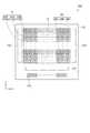
まず、本実施形態に係る有機EL装置100の概要について、図1乃至図3を参照して説明する。図1は有機EL装置の構成を示す概略平面図であり、図2は有機EL装置の電気的な構成を示す等価回路図である、図3は発光画素の特徴部分を示す概略平面図である。
なお、図3では、発光画素の特徴部分を説明するために必要な構成要素が図示され、他の構成要素の図示は省略されている。また図3における二点鎖線は、発光画素20の輪郭を示している。(Embodiment 1)
"Outline of organic EL device"
The
First, an outline of the
In FIG. 3, constituent elements necessary for explaining the characteristic part of the light emitting pixel are shown, and other constituent elements are not shown. In addition, a two-dot chain line in FIG.
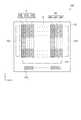
図1に示すように、本実施形態の有機EL装置100は、基板としての素子基板10、素子基板10の表示領域Eにマトリックス状に配置された複数の発光画素20B,20G,20R、複数の発光画素20B,20G,20Rを駆動制御する周辺回路であるデータ線駆動回路101及び走査線駆動回路102、外部回路との電気的な接続を図るための外部接続用端子103などを備えている。 As shown in FIG. 1, an
素子基板10の第1辺に沿って、複数の外部接続用端子103が配列されている。複数の外部接続用端子103と表示領域Eとの間には、データ線駆動回路101が設けられている。該第1辺と直交し互いに対向する他の第2辺、第3辺と表示領域Eとの間には、走査線駆動回路104が設けられている。
以降、該第1辺に沿った方向をX方向、及び該第1辺と直交し互いに対向する他の2辺(第2辺、第3辺)に沿った方向をY方向として説明する。
なお、X方向は、本発明における「第1の方向」の一例であり、Y方向は、本発明における「第2の方向」の一例である。A plurality of
Hereinafter, the direction along the first side will be described as the X direction, and the direction along the other two sides (second side and third side) orthogonal to the first side and facing each other will be described as the Y direction.
The X direction is an example of the “first direction” in the present invention, and the Y direction is an example of the “second direction” in the present invention.
有機EL装置100は、青色(B)の発光が得られる発光画素20Bと、緑色(G)の発光が得られる発光画素20Gと、赤色(R)の発光が得られる発光画素20Rとを有している。有機EL装置100では、X方向に配置された発光画素20Bと発光画素20Gと発光画素20Rとが表示単位Pとなって、フルカラーの表示が提供される。 The
さらに、発光画素20Bは画素電極31Bを有し、発光画素20Gは画素電極31Gを有し、発光画素20Rは画素電極31Rを有している。発光画素20B(画素電極31B)、発光画素20G(画素電極31G)、及び発光画素20R(画素電極31G)のそれぞれは、Y方向に並んで配置されている。
なお、画素電極31Bは本発明における「第1の画素電極」の一例であり、画素電極31Gは本発明における「第2の画素電極」の一例であり、画素電極31Rは本発明における「第3の画素電極」の一例である。
以降の説明では、発光画素20B,20G,20Rや画素電極31B,31G,31Rと称す場合と、これらをまとめて発光画素20や画素電極31と称す場合とがある。Further, the
The
In the following description, there are cases where the light-emitting
Y方向には、同じ色の発光が得られる発光画素20が配置されている。つまり、青色(B)の発光が得られる発光画素20Bは、Y方向に配置され、矩形状(ストライプ形状)をなしている。緑色(G)の発光が得られる発光画素20Gは、Y方向に配置され、矩形状(ストライプ形状)をなしている。赤色(R)の発光が得られる発光画素20Rは、Y方向に配置され、矩形状(ストライプ形状)をなしている。
X方向には、異なる色の発光が得られる発光画素20が、B,G,Rの順に繰り返して配置されている。なお、X方向における発光画素20の配置は、B,G,Rの順でなくてもよく、例えばR,G,Bの順であってもよい。In the Y direction,
In the X direction,
透光性の第1の絶縁層28が、外部接続用端子103の形成領域を除く素子基板10の略全面に設けられている。
透光性の第1の絶縁層28は、発光画素20B(画素電極31B)が配置される第1の領域28Bと、発光画素20G(画素電極31G)が配置される第2の領域28Gと、発光画素20R(画素電極31R)が配置される第3の領域28Rとを有し、それぞれの領域で第1の絶縁層28の層厚(膜厚)が異なる。詳細は後述するが、第2の領域28Gにおける第1の絶縁層28の膜厚は、第1の領域28Bにおける第1の絶縁層28の膜厚よりも大きくなっている。第3の領域28Rにおける第1の絶縁層28の膜厚は、第2の領域28Gにおける第1の絶縁層28の膜厚よりも大きくなっている。つまり、第1の絶縁層28の膜厚は、第1の領域28B、第2の領域28G、第3の領域28Rの順に大きくなっている。
第2の領域28Gは、本発明における「第1の平坦部」の一例である。第3の領域28Rは、本発明における「第2の平坦部」の一例である。A light-transmitting first insulating
The translucent first insulating
The
第1の領域28B、第2の領域28G及び第3の領域28Rは、Y方向に延在した矩形状(ストライプ形状)をなしている。
表示領域Eにおいて、第1の領域28B、第2の領域28G、及び第3の領域28RのX方向寸法は、発光画素20のX方向寸法と略同じ、つまり発光画素20のX方向の繰り返しピッチと略同じである。The
In the display area E, the X direction dimensions of the
Y方向において、第1の領域28B、第2の領域28G、及び第3の領域28Rは、表示領域Eよりも広くなっている。つまり、第1の領域28B、第2の領域28G、及び第3の領域のY方向寸法は、表示領域EのY方向寸法よりも大きくなっている。なお、第1の領域28B、第2の領域28G、及び第3の領域28RのY方向寸法は、表示領域EのY方向寸法、つまり発光画素20が配置された領域の寸法と同じであってもよい。 In the Y direction, the
第1の絶縁層28は、表示領域Eの周辺(第1の領域28B、第2の領域28G、及び第3の領域28R以外の領域)にも設けられている。本実施形態では、表示領域Eの周辺に設けられた第1の絶縁層28の膜厚は、第3の領域28Rの第1の絶縁層28の膜厚と同じなっている。なお、表示領域Eの周辺に設けられた第1の絶縁層28の膜厚は、第1の領域28Bの第1の絶縁層28の膜厚、または第2の領域28Gの第1の絶縁層28の膜厚と同じであってもよい。さらに、表示領域Eの周辺に設けられた第1の絶縁層28は、第1の領域28B、第2の領域28G、及び第3の領域28Rの第1の絶縁層28と異なる膜厚を有していてもよい。 The first insulating
なお、第1の領域28Bは本発明における「第1の層厚の部分」の一例であり、第2の領域28Gは本発明における「第2の層厚の部分」の一例であり、第3の領域28Rは本発明における「第3の層厚の部分」の一例である。 The
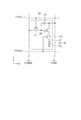
図2に示すように、素子基板10には、発光画素20に対応する信号線として、走査線11、データ線12、点灯制御線13、及び電源線14が設けられている。走査線11と点灯制御線13とはX方向に並行して延び、走査線駆動回路102(図1)に接続されている。データ線12と電源線14とはY方向に並行して延びている。データ線12は、データ線駆動回路101(図1)に接続されている。電源線14は、複数配置された外部接続用端子103のうちいずれかに接続されている。 As shown in FIG. 2, the
走査線11とデータ線12との交点付近には、発光画素20の画素回路を構成する第1トランジスター21と、第2トランジスター22と、第3トランジスター23と、蓄積容量24と、有機EL素子30とが設けられている。 Near the intersection of the
有機EL素子30は、陽極である画素電極31と、陰極である対向電極33と、これら電極の間に挟まれた発光層を含む発光機能層32とを有している。対向電極33は、複数の発光画素20に跨って設けられた共通電極である。対向電極33には、例えば電源線14に与えられる電源電圧Vddに対して低電位の、基準電位VssやGNDの電位などが与えられている。 The
第1トランジスター21及び第3トランジスター23は、例えばnチャネル型のトランジスターである。第2トランジスター22は、例えばpチャネル型のトランジスターである。 The
第1トランジスター21のゲート電極は走査線11に接続され、一方の電流端はデータ線12に接続され、他方の電流端は第2トランジスター22のゲート電極と、蓄積容量24の一方の電極とに接続されている。
第2トランジスター22の一方の電流端は、電源線14に接続されると共に蓄積容量24の他方の電極に接続されている。第2トランジスター22の他方の電流端は、第3トランジスター23の一方の電流端に接続されている。言い換えれば、第2トランジスター22と第3トランジスター23とは一対の電流端のうち1つの電流端を共有している。
第3トランジスター23のゲート電極は点灯制御線13に接続され、他方の電流端は有機EL素子30の画素電極31に接続されている。
第1トランジスター21、第2トランジスター22及び第3トランジスター23のそれぞれにおける一対の電流端は、一方がソースであり、他方がドレインである。
なお、第3トランジスター23は、本発明における「トランジスター」の一例である。The gate electrode of the
One current end of the
The gate electrode of the
One of the pair of current ends in each of the
The
このような画素回路において、走査線駆動回路102から走査線11に供給される走査信号Yiの電圧水準がHiレベルになると、nチェネル型の第1トランジスター21がオン状態(ON)となる。オン状態(ON)の第1トランジスター21を介してデータ線12と蓄積容量24とが電気的に接続される。そして、データ線駆動回路101からデータ線12にデータ信号が供給されると、データ信号の電圧水準Vdataと電源線14に与えられた電源電圧Vddとの電位差が蓄積容量24に蓄積される。 In such a pixel circuit, when the voltage level of the scanning signal Yi supplied from the scanning
走査線駆動回路102から走査線11に供給される走査信号Yiの電圧水準がLowレベルになると、nチェネル型の第1トランジスター21がオフ状態(OFF)となり、第2トランジスター22のゲート・ソース間電圧Vgsは、電圧水準Vdataが与えられたときの電圧に保持される。また、走査信号YiがLowレベルになった後に、点灯制御線13に供給される点灯制御信号Vgiの電圧水準がHiレベルとなり、第3トランジスター23がオン状態(ON)となる。そうすると、第2トランジスター22のゲート・ソース電圧Vgs、つまり蓄積容量24に保持された電圧に応じた電流が、電源線14から第2トランジスター22及び第3トランジスター23を経由して、有機EL素子30に供給される。 When the voltage level of the scanning signal Yi supplied from the scanning
有機EL素子30は、有機EL素子30を流れる電流の大きさに応じて発光する。有機EL素子30を流れる電流は、蓄積容量24に保持された電圧(データ線12の電圧水準Vdataと電源電圧Vddとの電位差)、及び第3トランジスター23がオン状態になる期間の長さによって変化し、有機EL素子30の発光輝度が規定される。つまり、データ信号における電圧水準Vdataの値により、発光画素20において画像情報に応じた輝度の階調性を与えることができる。 The
なお、本実施形態において、発光画素20の画素回路は、3つのトランジスター21,22,23を有することに限定されず、例えばスイッチング用トランジスターと駆動用トランジスターとを有する構成(二つのトランジスターを有する構成)としてもよい。また画素回路を構成するトランジスターは、nチャネル型のトランジスターでもよいし、pチャネル型のトランジスターでもよいし、nチャネル型のトランジスター及びpチャネル型のトランジスターの双方を備えるものであってもよい。また、発光画素20の画素回路を構成するトランジスターは、半導体基板にアクティブ層を有するMOS型トランジスターであってもよいし、薄膜トランジスターであってもよいし、電界効果トランジスターであってもよい。
また、走査線11、データ線12以外の信号線である点灯制御線13、電源線14の配置は、トランジスターや蓄積容量24の配置により左右され、これに限定されるものではない。
本実施形態では、発光画素20の画素回路を構成するトランジスターとして、半導体基板にアクティブ層を有するMOS型トランジスターを採用している。In the present embodiment, the pixel circuit of the
Further, the arrangement of the
In the present embodiment, a MOS transistor having an active layer on a semiconductor substrate is employed as the transistor constituting the pixel circuit of the
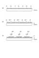
「発光画素の特徴部分」
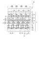
次に、図3を参照して、発光画素20の特徴部分の概要を説明する。
図3に示すように、発光画素20は、中継電極106と、画素電極31と、第2の絶縁層29とを有している。発光画素20では、中継電極106と、画素電極31と、第2の絶縁層29とが順に積層されている(図5、図6参照)。第2の絶縁層29は、画素電極31の一部を露出させる開口29B,29G,29Rを有している。青色(B)の発光が得られる発光画素20Bは、画素電極31Bと中継電極106Bと開口29Bとを有している。緑色(G)の発光が得られる発光画素20Gは、画素電極31Gと中継電極106Gと開口29Gとを有している。赤色(R)の発光が得られる発光画素20Rは、画素電極31Rと中継電極106Rと開口29Rとを有している。
以降の説明では、中継電極106B,106G,106Rと称す場合と、これらをまとめて中継電極106と称す場合とがある。
なお、中継電極106は、本発明における「導電層」の一例である。中継電極106Bは本発明における「第1の導電層」の一例であり、中継電極106Gは本発明における「第2の導電層」の一例であり、中継電極106Rは本発明における「第3の導電層」の一例である。"Characteristics of luminescent pixels"
Next, the outline of the characteristic part of the
As shown in FIG. 3, the
In the following description, there are cases where they are referred to as
The
発光画素20B,20G,20Rのそれぞれは、平面視で矩形状となっており、長手方向がY方向に沿って配置されている。同様に、画素電極31B,31G,31Rも、平面視で矩形状となっており、長手方向がY方向に沿って配置されている。 Each of the
同図に示すように、中継電極106は、矩形状の発光画素20の短い一辺に沿って配置され、平面視で少なくとも一部が画素電極31と重なるように設けられている。詳細は後述するが、中継電極106は、画素電極31と第3トランジスター23とを電気的に接続する配線の一部である。換言すれば、画素電極31は、中継電極106を介して第3トランジスター23に接続されている。つまり、中継電極106が設けられた領域がコンタクト領域となる。 As shown in the figure, the
第2の絶縁層29は、画素電極31の周縁部を覆い、隣り合う画素電極31同士を電気的に絶縁する役割を有している。上述したように、第2の絶縁層29は、画素電極31の一部を露出させる開口29B,29G,29Rを有している。第2の絶縁層29で露出された部分の画素電極31、つまり開口29B,29G,29Rで露出された画素電極31が発光機能層32に接し、発光機能層32に電流を供給し、発光機能層32を発光させる。このため、第2の絶縁層29に設けられた開口29B,29G,29Rが、発光画素20B,20G,20Rの発光領域となる。このように、第2の絶縁層29は、発光画素20の発光領域を規定する役割も有している。
なお、本願発明において、画素電極31は、発光領域(開口29B,29G,29R)において発光機能層32に接して有機EL素子30の電極として機能する電極部位と、トランジスターや配線と接続するコンタクト領域において電極部位と中継電極106とを接続する導電層として機能する導電部位とを少なくとも有している。The second insulating
In the present invention, the
詳細は後述するが、本実施形態の発光画素20は、発光領域(開口29B,29G,29R)とコンタクト領域(中継電極106B,106G,106R)との間の距離DYを小さくすることができる構成を有している。すなわち、発光領域(開口29B,29G,29R)を広くし、発光機能層32で発せられる光の光度を高めることができる構成を有している。この点が、発光画素20の特徴部分である。 Although details will be described later, the light-emitting
「発光画素の断面構造」
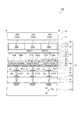
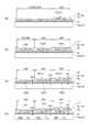
次に、発光画素20の断面構造について、図4乃至図8を参照して説明する。
図4は、図3のA−A’線に沿った概略断面図、つまり発光領域を規定する第2の絶縁層の開口が設けられた領域の概略断面図である。図5は、図3のB−B’線に沿った概略断面図、つまり画素電極と第3トランジスターとが電気的に接続された領域の概略断面図である。図6は、図3のC−C’線に沿った概略断面図、つまり赤色(R)の発光が得られる発光画素の概略断面図である。図7は、図3のD−D’線に沿った概略断面図、つまり緑色(G)の発光が得られる発光画素の概略断面図である。図8は、図3のE−E’線に沿った概略断面図、つまり青色(B)の発光が得られる発光画素の概略断面図である。"Cross-sectional structure of light-emitting pixels"
Next, a cross-sectional structure of the
4 is a schematic cross-sectional view taken along the line AA ′ in FIG. 3, that is, a schematic cross-sectional view of a region provided with an opening of a second insulating layer that defines a light emitting region. FIG. 5 is a schematic cross-sectional view taken along the line BB ′ of FIG. 3, that is, a schematic cross-sectional view of a region where the pixel electrode and the third transistor are electrically connected. FIG. 6 is a schematic cross-sectional view taken along the line CC ′ of FIG. 3, that is, a schematic cross-sectional view of a luminescent pixel that can emit red (R) light. FIG. 7 is a schematic cross-sectional view taken along the line DD ′ of FIG. 3, that is, a schematic cross-sectional view of a luminescent pixel that can emit green (G) light. FIG. 8 is a schematic cross-sectional view taken along the line EE ′ of FIG. 3, that is, a schematic cross-sectional view of a luminescent pixel that can emit blue (B) light.
なお、図4は、画素回路のうち、第1トランジスター21及び第2トランジスター22や、第1トランジスター21及び第2トランジスター22に関連する配線などを示し、第3トランジスター23の図示を省略している。図5は、画素回路のうち、第3トランジスター23や第3トランジスター23に関連する配線などを示し、第1トランジスター21及び第2トランジスターの図示を省略している。図6乃至図8では、第2トランジスター22及び第3トランジスター23や、第2トランジスター22及び第3トランジスター23に関連する配線などを示し、第1トランジスター21の図示を省略している。 FIG. 4 shows the
最初に、図4を参照して、発光領域を規定する第2の絶縁層29の開口29B,29G,29Rが設けられた領域の断面構造について説明する。
図4に示すように、有機EL装置100は、素子基板10、封止基板70、及び素子基板10と封止基板70とで挟持された樹脂層71などを有している。First, a cross-sectional structure of a region where the
As illustrated in FIG. 4, the
封止基板70は、透光性の絶縁基板であり、石英基板やガラス基板などを使用することができる。封止基板70は、表示領域Eに配置された有機EL素子30が傷つかないように保護する役割を有し、表示領域Eよりも広く設けられている。樹脂層71は、素子基板10と封止基板70とを接着する役割を有し、例えばエポキシ樹脂やアクリル樹脂などを使用することができる。 The sealing
素子基板10は、画素回路(第1トランジスター21、第2トランジスター22、第3トランジスター23、蓄積容量24、有機EL素子30)、封止層40、カラーフィルター50などを有している。 The
発光画素20で発せられた光は、カラーフィルター50を透過して封止基板70の側から射出される。つまり、有機EL装置100は、トップエミッション構造となっている。有機EL装置100がトップエミッション構造であることから、素子基板10の基材10sには、透明な石英基板やガラス基板だけでなく、不透明なセラミック基板や半導体基板を用いることができる。本実施形態では、基材10sには、半導体基板、例えばシリコン基板を使用している。 The light emitted from the
基材10sには、半導体基板にイオンを注入することによって形成されたウェル部10wと、ウェル部10wとは異なる種類のイオンをウェル部10wに注入することにより形成されたアクティブ層であるイオン注入部10dとが設けられている。ウェル部10wは、発光画素20におけるトランジスター21,22,23のチャネルとして機能する。イオン注入部10dは、発光画素20におけるトランジスター21,22,23のソース・ドレインや配線の一部として機能する。 In the
イオン注入部10dやウェル部10wが形成された基材10sの表面を覆うように、絶縁膜10aが設けられている。絶縁膜10aは、トランジスター21,22,23のゲート絶縁膜として機能する。絶縁膜10aの上には、例えばポリシリコンなどの導電膜からなるゲート電極22gが設けられている。ゲート電極22gは、第2トランジスター22のチャネルとして機能するウェル部10wに対向するように配置されている。他の第1トランジスター21や第3トランジスター23でも、同様にゲート電極が設けられている。 An insulating
ゲート電極22gを覆うように、第1層間絶縁膜15が設けられている。第1層間絶縁膜15には、例えば第1トランジスター21のドレインや第2トランジスター22のゲート電極22gに至るコンタクトホールが設けられている。このコンタクトホール内を少なくとも被覆し、第1層間絶縁膜15の表面を覆う導電膜が成膜され、これをパターニングすることにより、例えば第1トランジスター21のドレイン電極21dと第2トランジスター22のゲート電極22gとに接続される配線が設けられている。 A first
次に、第1層間絶縁膜15や、第1層間絶縁膜15の上の配線を覆うように、第2層間絶縁膜16が設けられている。第2層間絶縁膜16には、第1層間絶縁膜15の上に設けられた配線に至るコンタクトホールが設けられている。このコンタクトホール内を少なくとも被覆し、第2層間絶縁膜16の表面を覆う導電膜が成膜され、これをパターニングすることにより、例えば蓄積容量24の一方の電極24aと第2トランジスター22のゲート電極22gとを電気的に接続させるコンタクト部が設けられている。また、蓄積容量24の一方の電極24aと同層にデータ線12が設けられている。データ線12は、図4では図示省略された中継電極(配線)によって、第1トランジスター21のソースに接続されている。 Next, a second
図示を省略するが、少なくとも蓄積容量24の一方の電極24aを覆う誘電体層が設けられている。また、蓄積容量24の他方の電極24bが、誘電体層を挟んで、蓄積容量24の一方の電極24aに対向して設けられている。これにより、これら一対の電極24a,24bと誘電体層とによって、蓄積容量24が形成されている。 Although not shown, a dielectric layer covering at least one
蓄積容量24を覆うように、第3層間絶縁膜17が設けられている。第3層間絶縁膜17には、例えば蓄積容量24の他方の電極24bや第2層間絶縁膜16上に形成された配線に至るコンタクトホールが設けられている。このコンタクトホール内を少なくとも被覆し、第3層間絶縁膜17の表面を覆う導電膜が成膜され、これをパターニングすることにより、電源線14や中継電極14c(図5参照)などが設けられている。本実施形態では、電源線14及び中継電極14cは、光反射性と導電性とを兼ね備えた導電材料、例えばアルミニウムやアルミニウム合金などで構成されている。電源線14及び中継電極14cの膜厚は、概略100nmである。 A third
電源線14は、表示領域Eの略全面に設けられ、発光画素20B,20G,20Rのそれぞれに開口を有している。電源線14の開口の中に、中継電極14cが設けられている。電源線14は、トランジスター21,22,23の上方で、画素電極31に対向するように配置されている。発光領域(開口29B,29G,29R)で発した光は、電源線14で反射される。
電源線14は、本発明における「光反射層」の一例である。
なお、発光領域(開口29B,29G,29R)で発した光を反射する光反射層を、画素電極31ごとに島状に設ける構成であってもよい。The
The
In addition, the structure which provides the light reflection layer which reflects the light emitted in the light emission area | region (opening 29B, 29G, 29R) for every
電源線14の上には、第1絶縁膜25と、第2絶縁膜26と、第3絶縁膜27とが、順に積層されている。第1絶縁膜25、第2絶縁膜26、及び第3絶縁膜27は、光透過性を有する絶縁材料で構成されている。本実施形態では、第1絶縁膜25が窒化シリコンで構成され、第2絶縁膜26及び第3絶縁膜27が酸化シリコンで構成されている。第1絶縁膜25の膜厚は、概略50nmである。第2絶縁膜26及び第3絶縁膜27の膜厚は、概略60nm〜70nmである。 On the
第1絶縁膜25は、青色(B)の発光が得られる発光画素20Bと、緑色(G)の発光が得られる発光画素20Gと、赤色(R)の発光が得られる発光画素20Rとに設けられている。第2絶縁膜26は、緑色(G)の発光が得られる発光画素20Gと、赤色(R)の発光が得られる発光画素20Rとに設けられている。第3絶縁膜27は、赤色(R)の発光が得られる発光画素20Rに設けられている。 The first insulating
第1の絶縁層28は、第1絶縁膜25と、第2絶縁膜26と、第3絶縁膜27とで構成される。
詳しくは、青色(B)の発光が得られる発光画素20Bの第1の絶縁層28は、第1絶縁膜25で構成され、膜厚Bd1を有している。そして、発光画素20Bにおいて、膜厚Bd1を有する第1の絶縁層28は、中継電極106Bと画素電極31Bとを接続するコンタクト領域を除き、開口29B(発光領域)からコンタクト領域に至るように設けられている。また、膜厚Bd1を有する第1の絶縁層28は、Y方向に並ぶ複数の発光画素20Bに跨って設けられている。また、換言すると、第1の領域28Bには、Y方向に並ぶ開口29B(発光領域)が複数設けられている。また、第1の領域28B内に中継電極106Bと画素電極31Bとを接続するコンタクト領域が設けられている。図5に示すように、当該コンタクト領域において、画素電極31Bは中継電極106Bに直接接している。The first insulating
Specifically, the first insulating
緑色(G)の発光が得られる発光画素20Gの第1の絶縁層28は、第1絶縁膜25と第2絶縁膜26とで構成され、膜厚Gd1を有している。そして、発光画素20Gにおいて、膜厚Gd1を有する第1の絶縁層28は、中継電極106Gと画素電極31Gとを接続するコンタクト領域を除き、開口29G(発光領域)からコンタクト領域に至るように設けられている。膜厚Gd1を有する第1の絶縁層28は、Y方向に並ぶ複数の発光画素20Gに跨って設けられている。また、換言すると、第2の領域28Gには、Y方向に並ぶ開口29G(発光領域)が複数設けられている。また、第2の領域28G内に中継電極106Gと画素電極31Gとを接続するコンタクト領域が設けられている。図5に示すように、当該コンタクト領域において、画素電極31Gはコンタクトホール28CT1を介して中継電極106Gに接続されている。 The first insulating
赤色(G)の発光が得られる発光画素20Gの第1の絶縁層28は、第1絶縁膜25と第2絶縁膜26と第3絶縁膜27とで構成され、膜厚Rd1を有している。そして、発光画素20Rにおいて、膜厚Rd1を有する第1の絶縁層28は、中継電極106Rと画素電極31Rとを接続するコンタクト領域を除き、開口29R(発光領域)からコンタクト領域に至るように設けられている。膜厚Rd1を有する第1の絶縁層28は、Y方向に並ぶ複数の発光画素20Rに跨って設けられている。また、換言すると、第3の領域28Rには、Y方向に並ぶ開口29R(発光領域)が複数設けられている。第3の領域28R内に中継電極106Rと画素電極31Rとを接続するコンタクト領域が設けられている。図5に示すように、当該コンタクト領域において、画素電極31Rはコンタクトホール28CT2を介して中継電極106Rに接続されている。 The first insulating
このため、発光画素20Bの第1の絶縁層28(膜厚Bd1)、発光画素20Gの第1の絶縁層28(膜厚Gd1)、発光画素20Rの第1の絶縁層28(膜厚Rd1)の順に厚くなっている。 Therefore, the first insulating layer 28 (film thickness Bd1) of the
換言すれば、第1絶縁膜25で構成された第1の絶縁層28、つまり発光画素20Bが配置された領域の第1の絶縁層28が、第1の領域28Bに対応する。第1絶縁膜25と第2絶縁膜26とで構成された第1の絶縁層28、つまり発光画素20Gが配置された領域の第1の絶縁層28が、第2の領域28Gに対応する。第1絶縁膜25と第2絶縁膜26と第3絶縁膜27とで構成された第1の絶縁層28、つまり発光画素20Rが配置された領域の第1の絶縁層28が、第3の領域28Rに対応する。
なお、膜厚Bd1は、本発明における「第1の層厚」の一例である。膜厚Gd1は、本発明における「第2の層厚」の一例である。膜厚Rd1は、本発明における「第3の層厚」の一例である。In other words, the first insulating
The film thickness Bd1 is an example of the “first layer thickness” in the present invention. The film thickness Gd1 is an example of the “second layer thickness” in the present invention. The film thickness Rd1 is an example of the “third layer thickness” in the present invention.
画素電極31は、第1の絶縁層28の上に島状に設けられ、第1の絶縁層28を挟んで電源線14に対向する。詳しくは、画素電極31Bは膜厚Bd1の第1の絶縁層28の上に島状に設けられ、画素電極31Gは膜厚Gd1の第1の絶縁層28の上に島状に設けられ、画素電極31Rは膜厚Bd1の第1の絶縁層28の上に島状に設けられている。画素電極31は、光透過性を有し、例えばITO(Indium Tin Oxide)などの光透過性材料で形成され、発光機能層32に正孔を供給するための電極となる。画素電極31の膜厚は、概略100nmである。 The
画素電極31の周縁部を覆うように、第2の絶縁層29が設けられている。第2の絶縁層29は、例えば酸化シリコンで構成され、各画素電極31R,31G,31Bのそれぞれを絶縁している。第2の絶縁層29の膜厚は、概略60nmである。第2の絶縁層29には、開口29B,29G,29Rが設けられている。開口29B,29G,29Rが設けられた領域が、発光画素20の発光領域となる。なお、第2の絶縁層29は、有機材料、例えばアクリル系の感光性樹脂を用いて形成してもよい。
画素電極31及び第2の絶縁層29を覆うように、発光機能層32と、対向電極33と封止層40とが、順に積層されている。A second insulating
A light emitting
発光機能層32は、画素電極31の側から順に積層された正孔注入層、正孔輸送層、有機発光層、及び電子輸送層などを有している。画素電極31から供給される正孔と、対向電極33から供給される電子とが有機発光層で結合し、発光機能層32が発光する(光を発する)。発光機能層32の膜厚は、概略110nmである。
有機発光層は、赤色、緑色、及び青色の光成分を有する光を発する。有機発光層は、単層で構成してもよいし、複数の層(例えば、電流が流れると主に青色で発光する青色発光層と、電流が流れると赤色と緑色を含む光を発する黄色発光層)で構成してもよい。The light emitting
The organic light emitting layer emits light having red, green, and blue light components. The organic light emitting layer may be composed of a single layer, or a plurality of layers (for example, a blue light emitting layer that emits mainly blue light when current flows, and yellow light that emits light including red and green when current flows) Layer).
対向電極33は、発光機能層32に電子を供給するための共通電極である。対向電極33は、発光機能層32を覆って設けられ、例えばMgとAgとの合金などで構成され、光透過性と光反射性とを有している。対向電極33の膜厚は、概略10nm〜30nmである。対向電極33の構成材料(MgとAgとの合金など)を薄膜化することで、光反射性の機能に加えて光透過性の機能を付与することができる。 The
対向電極33の上には、封止層40が配置されている。封止層40は、発光機能層32や対向電極33の劣化を抑制するパッシベーション膜であり、発光機能層32や対向電極33への水分や酸素の侵入を抑制している。封止層40は、対向電極33の側から順に積層された第1封止層41と緩衝層42と第2封止層43とで構成され、有機EL素子30(表示領域E)を覆い、素子基板10の略全面に設けられている。なお、封止層40には、外部接続用端子103端子(図1参照)を露出させる開口(図示省略)が設けられている。 A
第1封止層41は、例えば公知技術のプラズマCVD(Chemical Vapor Deposition)法などを用いて形成されたシリコン酸窒化物で構成され、水分や酸素に対して高いバリア性を有している。第1封止層41の膜厚は、概略200nm〜400nmである。第1封止層41を構成する材料は、上述したシリコン酸窒化物の他に、シリコン酸化物、シリコン窒化物、及び酸化チタンなどの金属酸化物などを使用することができる。 The
緩衝層42は、熱安定性に優れた例えばエポキシ系樹脂や塗布型の無機材料(シリコン酸化物など)などで構成されている。緩衝層42の膜厚は、第1封止層41の膜厚よりも大きく、概略1000nm〜5000nmである。緩衝層42は、第1封止層41の欠陥(ピンホール、クラック)や異物などを被覆し、緩衝層42における第2封止層43側の面は、対向電極33側の面に比べ平坦な面を形成する。 The
第2封止層43は、例えば公知技術のプラズマCVD法などを用いて形成されたシリコン酸窒化物で構成される。第2封止層43の膜厚は、概略300nm〜700nmである。第2封止層43は、第1封止層41と同じ材料で構成され、水分や酸素に対して高いバリア性を有している。 The
封止層40の上には、発光画素20B,20G,20Rに対応した着色層50B,50G,50Rが設けられている。換言すれば、封止層40の上には、着色層50B,50G,50Rで構成されるカラーフィルター50が設けられている。ここで、カラーフィルター50は、封止層40の上に積層して設けられている。 On the
次に、図5を参照して、画素電極31と第3トランジスター23とが電気的に接続された部分(コンタクト部)の断面構造について説明する。 Next, a cross-sectional structure of a portion (contact portion) where the
図5に示すように、基材10sには、第3トランジスター23のソースとして機能するイオン注入部10dが設けられている。イオン注入部10d(基材10s)は、絶縁膜10aと第1層間絶縁膜15とで覆われている。第1層間絶縁膜15及び絶縁膜10aには、第3トランジスター23のイオン注入部10dに至るコンタクトホールが設けられている。このコンタクトホール内を少なくとも被覆し、第1層間絶縁膜15の表面を覆う導電膜が成膜され、これをパターニングすることにより、第3トランジスター23のソース電極23s及び当該ソース電極23sに接続される配線が設けられている。 As shown in FIG. 5, the
第1層間絶縁膜15及びソース電極23sに接続される配線は、第2層間絶縁膜16で覆われている。第2層間絶縁膜16には、ソース電極23sに接続される配線に至るコンタクトホールが設けられている。このコンタクトホール内を少なくとも被覆し、第2層間絶縁膜16の表面を覆う導電膜が成膜され、これをパターニングすることにより、第2層間絶縁膜16の上に配線が設けられている。第2層間絶縁膜16は、第3層間絶縁膜17で覆われている。第3層間絶縁膜17には、第2層間絶縁膜16の上に設けられた配線に至るコンタクトホールが設けられている。このコンタクトホール内を少なくとも被覆し、第3層間絶縁膜17の表面を覆う導電膜が成膜され、これをパターニングすることにより、第3層間絶縁膜17の上に電源線14及び中継電極14cが設けられている。 The wiring connected to the first
上述したように、電源線14は、表示領域Eの略全面に設けられ、発光画素20B,20G,20Rのそれぞれに開口を有している。中継電極14cは、電源線14の開口の中に、発光画素20B,20G,20Rのそれぞれに島状に設けられている。また、中継電極14cは、画素電極31と第3トランジスター23とを電気的に接続する配線の一部をなす。 As described above, the
電源線14及び中継電極14cを覆うように、第1絶縁膜25が設けられている。第1絶縁膜25には、中継電極14cの一部を露出させるコンタクトホール61CTが設けられている。コンタクトホール61CT内を少なくとも被覆し、第1絶縁膜25の表面を覆う導電膜が成膜され、これをパターニングすることにより、第1絶縁膜25の上に中継電極106が設けられている。中継電極106は、コンタクトホール61CTを介して中継電極14cに、接続されている。中継電極106は、画素電極31と第3トランジスター23とを電気的に接続する配線の一部をなす。 A first insulating
中継電極106は、遮光性の導電材料、例えば窒化チタンで構成される。中継電極106の膜厚は、概略50nmである。中継電極106は、平面視で電源線14の開口を覆うように、発光画素20B,20G,20Rのそれぞれに島状に設けられている。換言すれば、中継電極106は、発光機能層32で発した光が、電源線14の開口を通過してトランジスター21,22,23に入射しないように設けられている。すなわち、中継電極106は、発光機能層32で発した光の入射を遮り、トランジスター21,22,23の誤動作を抑制する役割も有している。 The
画素電極31は、平面視で中継電極106と重なるように設けられている。上述したように、発光画素20Bには中継電極106Bと画素電極31Bとが設けられ、発光画素20Gには中継電極106Gと画素電極31Gとが設けられ、発光画素20Rには中継電極106Rと画素電極31Rとが設けられている。 The
発光画素20Bにおいて、画素電極31Bは中継電極106Bに直接接している。 In the
発光画素20Gにおいて、中継電極106Gと画素電極31Gとの間には、第2絶縁膜26が設けられている。第2絶縁膜26には、中継電極106Gの一部を露出させるコンタクトホール28CT1が設けられている。画素電極31Bは、コンタクトホール28CT1を介して中継電極106Gに接続されている。 In the
発光画素20Rにおいて、中継電極106Rと画素電極31Rとの間には、中継電極106Rの側から順に第2絶縁膜26と第3絶縁膜27とが設けられている(積層されている)。第2絶縁膜26及び第3絶縁膜27には、中継電極106Rの一部を露出させるコンタクトホール28CT2が設けられている。画素電極31Rは、コンタクトホール28CT2を介して中継電極106Rに接続されている。
なお、コンタクトホール28CT1は、本発明における「第1のコンタクトホール」の一例である。コンタクトホール28CT2は、本発明における「第2のコンタクトホール」の一例である。In the
The contact hole 28CT1 is an example of the “first contact hole” in the present invention. The contact hole 28CT2 is an example of the “second contact hole” in the present invention.
このように、中継電極14cと中継電極106との間に配置される絶縁膜は、発光画素20B、20G,20Rのそれぞれで共通(第1絶縁膜25)である。さらに、電源線14と画素電極31との間に配置される第1の絶縁層28の膜厚は、発光画素20B、20G,20Rのそれぞれで異なっている。詳しくは、発光画素20Bでは、電源線14と画素電極31との間に、第1絶縁膜25で構成される膜厚Bd1の第1の絶縁層28が配置されている。発光画素20Gでは、電源線14と画素電極31との間に、第1絶縁膜25と第2絶縁膜26とで構成される膜厚Gd1の第1の絶縁層28が配置されている。発光画素20Rでは、電源線14と画素電極31との間に、第1絶縁膜25と第2絶縁膜26とで第3絶縁膜27とで構成される膜厚Rd1の第1の絶縁層28が配置されている。 Thus, the insulating film disposed between the
ここで、本実施形態では、第1絶縁膜25が窒化シリコンで構成され、第2絶縁膜26及び第3絶縁膜27が酸化シリコンで構成されている。そして、中継電極14cと中継電極106との間に配置される絶縁膜を窒化シリコンとすることで、酸化シリコンで構成される第2絶縁膜26及び第3絶縁膜27を加工する際に、第1絶縁膜25に対するエッチングの選択比を確保できるため加工精度を向上させることができるとともに、中継電極14cと画素電極31とを確実に接続することができる。 Here, in the present embodiment, the first insulating
第1の領域28Bでは、膜厚Bd1の第1の絶縁層28(第1絶縁膜25)の上に画素電極31Bが設けられ、画素電極31Bは中継電極106Bに直接接している。第2の領域28Gでは、膜厚Gd1の第1の絶縁層28(第1絶縁膜25と第2絶縁膜26)の上に画素電極31Gが設けられ、画素電極31Gはコンタクトホール28CT1を介して中継電極106Gに接続されている。第3の領域28Rでは、膜厚Rd1の第1の絶縁層28(第1絶縁膜25と第2絶縁膜26と第3絶縁膜27)の上に画素電極31Rが設けられ、画素電極31Rはコンタクトホール28CT2を介して中継電極106Rに接続されている。 In the
第1の領域28Bに設けられた画素電極31B、第2の領域28Gに設けられた画素電極31G、及び第3の領域28Rに設けられた画素電極31Rは、第2の絶縁層29で覆われている。さらに、第2の絶縁層29の上には、発光機能層32と、対向電極33と、封止層40と、カラーフィルター50とが順に設けられている(積層されている)。 The
次に、図6乃至図8を参照して、発光画素20におけるY方向の断面構造について説明する。
図6乃至図8に示すように、基材10sには、第2トランジスター22と第3トランジスター23とが共用するウェル部10wが設けられている。当該ウェル部10wには、3つのイオン注入部10dが設けられている。3つのイオン注入部10dのうち中央側に位置するイオン注入部10dは、第2トランジスター22と第3トランジスター23とが共用するドレイン22d(23d)として機能するものである。当該ウェル部10wを覆う絶縁膜10aが設けられる。そして、絶縁膜10aの上には、例えばポリシリコンなどの導電膜からなるゲート電極22g,23g(第2トランジスター22のゲート電極22g、第3トランジスター23のゲート電極23g)が設けられている。ゲート電極22g,23gのそれぞれは、中央側のイオン注入部10dと端側のイオン注入部10dとの間のウェル部10wにおけるチャネルとして機能する部分に対向するように配置されている。Next, the cross-sectional structure in the Y direction of the
As shown in FIGS. 6 to 8, the base 10 s is provided with a
次に、第2トランジスター22のゲート電極22gは、第1層間絶縁膜15と第2層間絶縁膜16とを貫通するコンタクトホールによって、第2層間絶縁膜16上に設けられた蓄積容量24の一方の電極24aに接続されている。第2トランジスター22のソース電極22sは、第1層間絶縁膜15と第2層間絶縁膜16と第3層間絶縁膜17とを貫通するコンタクトホールによって、第3層間絶縁膜17上に設けられた電源線14に接続されている。 Next, the
第3トランジスター23のゲート電極23gは、第1層間絶縁膜15を貫通するコンタクトホールによって、第1層間絶縁膜15上に設けられた点灯制御線13に接続されている。第1層間絶縁膜15上には、点灯制御線13以外に走査線11が設けられている。走査線11は、図5には図示されていないコンタクトホールを経由して、第1トランジスター21のゲートに接続されている。 The gate electrode 23 g of the
第3トランジスター23のソース電極23sは、第1層間絶縁膜15と第2層間絶縁膜16と第3層間絶縁膜17とを貫通するコンタクトホールによって、第3層間絶縁膜17上に設けられた中継電極14cに接続されている。中継電極14cは、第1絶縁膜25で覆われ、コンタクトホール25CTを介して、第1絶縁膜25の上に設けられた中継電極106に接続されている。 The source electrode 23 s of the
発光画素20Rでは、画素電極31Rが、第2絶縁膜26及び第3絶縁膜27に設けられたコンタクトホール28CT2を介して中継電極106Rに接続されている。
図6のように、第2絶縁膜26及び第3絶縁膜27は、コンタクトホール28CT2を介して画素電極31Rと中継電極106Rとが接続されるコンタクト領域を除いて発光画素20Rに設けられている。第1絶縁膜25は、コンタクトホール25CTを介して中継電極106Rと中継電極14cとが接続されるコンタクト領域を除いて発光画素20Rに設けられている。コンタクトホール28CT2、中継電極106R、コンタクトホール25CTは、本発明における「第3接続部」の一例である。第3接続部は、第3の領域28R(第3の層厚の部分)に設けられている。第3接続部は、第1絶縁膜25、第2絶縁膜26及び第3絶縁膜27により囲まれている。そして、第3の領域28R(第3の層厚の部分)には、開口29R(発光領域)がY方向に並んでいる。また、第1絶縁膜25、第2絶縁膜26及び第3絶縁膜27は、第3接続部の間を埋めるように設けられている。したがって、開口29R(発光領域)とコンタクト領域との間には第1の絶縁層28による段差がなく、段差がある場合と比して発光領域(開口29R)とコンタクト領域(中継電極106G)との間の距離DYを小さくできる。換言すると、開口29R(発光領域)を図6の右側のコンタクト領域に近づけることが可能である。さらに、開口29R(発光領域)を図6の左側のコンタクト領域にも近づけることが可能である。したがって、開口29R(発光領域)を大きくすることができる。In the
As shown in FIG. 6, the second insulating
発光画素20Gでは、画素電極31Gが、第2絶縁膜26に設けられたコンタクトホール28CT1を介して中継電極106Gに接続されている。
図7のように、第2絶縁膜26は、コンタクトホール28CT1を介して画素電極31Gと中継電極106Gとが接続されるコンタクト領域を除いて発光画素20Gに設けられている。また、第1絶縁膜25は、コンタクトホール25CTを介して中継電極106Gと中継電極14cとが接続される領域を除いて発光画素20Gに設けられている。コンタクトホール28CT1、中継電極106G、コンタクトホール25CTは、本発明における「第2接続部」「第4接続部」の一例である。第2接続部及び第4接続部は、第2の領域28G(第2の層厚の部分)に設けられている。第2接続部及び第4接続部は、第1絶縁膜25及び第2絶縁膜26により囲まれている。そして、第2の領域28G(第2の層厚の部分)には、開口29G(発光領域)がY方向に並んでいる。また、第1絶縁膜25及び第2絶縁膜26は、第2接続部と第4接続部との間を埋めるように設けられている。したがって、開口29G(発光領域)とコンタクト領域との間には第1の絶縁層28による段差がなく、段差がある場合と発光領域(開口29G)とコンタクト領域(中継電極106G)との間の距離DYを小さくできる。換言すると、開口29G(発光領域)を図7の右側のコンタクト領域に近づけることが可能である。さらに、開口29G(発光領域)を図7の左側のコンタクト領域にも近づけることが可能である。したがって、開口29G(発光領域)を大きくすることができる。In the
As shown in FIG. 7, the second insulating
発光画素20Bでは、画素電極31Bが中継電極106Bに直接接している。
図8のように、コンタクトホール25CTを介して中継電極106Bと中継電極14cとが接続されるコンタクト領域を除き、第1絶縁膜25が設けられている。コンタクトホール25CT、中継電極106Bは、本発明における「第1接続部」の一例である。第1接続部は、第1の領域(第1の層厚の部分)に設けられている。第2接続部は、第1絶縁膜25、第1絶縁膜25及び第2絶縁膜26により囲まれている。そして第1の領域(第1の層厚の部分)には、開口29B(発光領域)がY方向に並んでいる。また、第1絶縁膜25は、第1接続部の間を埋めるように設けられている。したがって、開口29B(発光領域)とコンタクト領域との間には第1の絶縁層28による段差がなく、段差がある場合と比して発光領域(開口29B)とコンタクト領域(中継電極106G)との間の距離DYを小さくできる。換言すると、開口29B(発光領域)を図8の右側のコンタクト領域に近づけることが可能である。さらに、開口29R(発光領域)を図8の左側のコンタクト領域にも近づけることが可能である。したがって、開口29B(発光領域)を大きくすることができる。
画素電極31の上には、第2の絶縁層29と、発光機能層32と、対向電極33と、封止層40と、カラーフィルター50とが順に積層されている。In the
As shown in FIG. 8, the first insulating
On the
「光共振構造」
発光領域(開口29B,29G,29R)には、光反射性を有する電源線14と、第1の絶縁層28と、画素電極31と、発光機能層32と、光反射性と光透過性とを有する対向電極33とが積層されている。かかる構成によって、発光機能層32で発した光を電源線14と対向電極33との間で往復させ(反射し)、特定波長の光を共振させる。これにより特定波長の光が他の波長領域に比べて強められ、有機EL素子30から出射する。さらに、特定波長の光は、電源線14から対向電極33に向かう方向、つまり封止基板70から表示光として射出される。このように、有機EL装置100は、電源線14と第1の絶縁層28と画素電極31と発光機能層32と対向電極33とで構成される光共振構造を有し、特定波長の光を選択的に強めて、発光画素20から発する光の色純度を高める構成を有している。
以下に光共振構造の概要を説明する。"Optical resonance structure"
In the light emitting region (
The outline of the optical resonant structure will be described below.
第1の絶縁層28は、電源線14と対向電極33との間の光路長(光学的な距離)を調整する役割を有し、第1の絶縁層28の膜厚に応じて共振波長が変化するようになっている。詳しくは、電源線14から対向電極33までの光学的な距離をD、反射層での反射における位相シフトをφL、対向電極33での反射における位相シフトをφU、定在波のピーク波長をλ、整数をmとすると、光学的な距離Dは、下記の数式(1)を満たすようになっている。
D={(2πm+φL+φU)/4π}λ・・・(1)The first insulating
D = {(2πm + φL + φU) / 4π} λ (1)
発光画素20B,20G,20Rの光共振構造における光学的な距離Dは、B,G,Rの順に大きくなり、電源線14と画素電極31との間に配置された第1の絶縁層28の膜厚を異ならせることによって調整されている。 The optical distance D in the optical resonance structure of the light-emitting
図6に示すように、発光画素20Rでは、電源線14と画素電極31Rとの間に配置される第1の絶縁層28は、第1絶縁膜25と第2絶縁膜26と第3絶縁膜27とで構成され、膜厚Rd1を有している。図7に示すように、発光画素20Gでは、電源線14と画素電極31Gとの間に配置される第1の絶縁層28は、第1絶縁膜25と第2絶縁膜26とで構成され、膜厚Gd1を有している。図8に示すように、発光画素20Bでは、電源線14と画素電極31Bとの間に配置される第1の絶縁層28は、第1絶縁膜25で構成され、膜厚Bd1を有している。このため、第1の絶縁層28の膜厚は、発光画素20B(膜厚Bd1)<発光画素20G(膜厚Gd1)<発光画素20R(膜厚Rd1)の順に大きくなる。このため、光学的な距離Dも、発光画素20B<発光画素20G<発光画素20Rの順に大きくなる。 As shown in FIG. 6, in the
詳しくは、発光画素20Rでは、共振波長(輝度が最大となるピーク波長)が610nmとなるように、光学的な距離Dが設定されている。同じく、発光画素20Gでは、共振波長(輝度が最大となるピーク波長)が540nmとなるように、光学的な距離Dが設定されている。発光画素20Bでは、共振波長(輝度が最大となるピーク波長)が470nmとなるように、光学的な距離Dが設定されている。 Specifically, in the
上記ピーク波長を実現するため、ITOなどの透明導電膜からなる画素電極31B,31G,31Rの膜厚を概略100nmとし、発光機能層32の膜厚を概略110nmとし、上記数式(1)においてm=1として、反射層と対向電極33との間の第1の絶縁層28の膜厚を算出すると、発光画素20Rでは170nm、発光画素20Gでは115nm、及び発光画素20Bでは50nmとなる。すなわち、発光画素20R(第3の領域28R)における第1の絶縁層28の膜厚Rd1は概略170nm、発光画素20G(第2の領域28G)における第1の絶縁層28の膜厚Gd1は概略115nm、発光画素20B(第1の領域28B)における第1の絶縁層28の膜厚Bd1は概略50nmとなる。このような第1の絶縁層28が形成されるように、第1絶縁膜25、第2絶縁膜26、及び第3絶縁膜27の膜厚が調整されている。 In order to realize the peak wavelength, the film thickness of the
その結果、発光画素20Rから610nmをピーク波長とする赤色(R)の光が発せられ、発光画素20Gから540nmをピーク波長とする緑色(G)の光が発せられ、発光画素20Bから470nmをピーク波長とする青色(B)の光が発せられる。
このように、本実施形態に係る有機EL装置100では、上述した光共振構造によって発光画素20から発する光の色純度を高め、鮮やかな表示を提供することができる。As a result, red (R) light having a peak wavelength of 610 nm is emitted from the
As described above, in the
図6に示すように、発光画素20Rでは、開口29Rが設けられた領域が発光領域となり、中継電極106Rが設けられた領域がコンタクト領域となる。画素電極31Rは、発光領域及びコンタクト領域に跨って配置されている。画素電極31Rが配置された領域の第1の絶縁層28の膜厚はRd1であるので、光学的な距離Dも一定になっている。このため、発光領域(開口29R)を広くし、発光領域(開口29R)とコンタクト領域(中継電極106R)との間の距離DYを小さくしても、発光領域における光学的な距離Dは一定であり、610nmをピーク波長とする赤色(R)の光が発せられる。すなわち、発光領域から発する光のピーク波長を維持して、赤色(R)の光の光度を高めることができる。 As shown in FIG. 6, in the
図7に示すように、発光画素20Gでは、開口29Gが設けられた領域が発光領域となり、中継電極106Gが設けられた領域がコンタクト領域となる。画素電極31Gは、発光領域及びコンタクト領域に跨って配置されている。画素電極31Gが配置された領域の第1の絶縁層28の膜厚はGd1であるので、光学的な距離Dも一定になっている。このため、発光領域(開口29G)を広くし、発光領域(開口29R)とコンタクト領域(中継電極106G)との間の距離DYを小さくしても、発光領域における光学的な距離Dは一定であり、540nmをピーク波長とする緑色(G)の光が発せられる。すなわち、発光領域から発する光のピーク波長を維持して、緑色(G)の光の光度を高めることができる。 As shown in FIG. 7, in the
図8に示すように、発光画素20Bでは、開口29Bが設けられた領域が発光領域となり、中継電極106Bが設けられた領域がコンタクト領域となる。画素電極31Bは、発光領域及びコンタクト領域に跨って配置されている。画素電極31Bが配置された領域の第1の絶縁層28の膜厚はBd1であるので、光学的な距離Dも一定になっている。このため、発光領域(開口29B)を広くし、発光領域(開口29B)とコンタクト領域(中継電極106B)との間の距離DYを小さくしても、発光領域における光学的な距離Dは一定であり、470nmをピーク波長とする青色(B)の光が発せられる。すなわち、発光領域から発する光のピーク波長を維持して、青色(B)の光の光度を高めることができる。 As shown in FIG. 8, in the
例えば、公知技術(特開2009−134067号公報)では、発光領域における光学的な距離とコンタクト領域における光学的な距離とが異なり、発光領域とコンタクト領域との間に、異なる光学的な距離の境界を有している。仮に、当該境界を越えて発光領域を広くすると、発光領域に光学的な距離が異なる部分が生じ、発光領域からピーク波長が異なる光が発せられ、発光領域から発する光の色純度が悪くなる。このため、公知技術では、当該境界を越えて発光領域を広くすることが難しい。 For example, in the known technique (Japanese Patent Laid-Open No. 2009-134067), the optical distance in the light emitting region is different from the optical distance in the contact region, and different optical distances exist between the light emitting region and the contact region. Has a boundary. If the light emitting region is widened beyond the boundary, a portion having a different optical distance is generated in the light emitting region, light having a different peak wavelength is emitted from the light emitting region, and the color purity of light emitted from the light emitting region is deteriorated. For this reason, it is difficult for the known technique to widen the light emitting region beyond the boundary.
本実施形態では、発光領域とコンタクト領域との間で光学的な距離Dは一定であるので、公知技術と比べて発光領域を広くし、発光領域から発する光の光度を高めることができる。
このように、本実施形態に係る有機EL装置100では、明るく鮮やかな表示を提供することができる。In the present embodiment, since the optical distance D is constant between the light emitting region and the contact region, the light emitting region can be widened compared to the known technique, and the luminous intensity of light emitted from the light emitting region can be increased.
Thus, the
なお、発光機能層32の発光に悪影響がない範囲で、発光領域(開口29B、29G、29R)を広くすることができる。例えば、発光機能層32の発光に悪影響がないのであれば、コンタクト領域(中継電極106B,106G,106R)の少なくとも一部に重なるように、発光領域(開口29B、29G、29R)を広げてもよい。 Note that the light emitting region (
「有機EL装置の製造方法」
次に、図9乃至図11を参照して、有機EL装置100の製造方法を説明する。図9は、有機EL装置の製造方法を示す工程フローである。図10及び図11は、図5に対応し、図9に示す各工程を経た後の有機EL装置の状態を示す概略断面図である。なお、図10及び図11では、素子基板10における電源線14よりも下層に設けられた画素回路や配線の図示を省略している。"Method for manufacturing organic EL device"
Next, a method for manufacturing the
図9に示すように、有機EL装置100を製造する工程は、光反射層としての電源線14を形成する工程(ステップS1)と、第1絶縁膜25を形成する工程(ステップS2)と、中継電極106を形成する工程(ステップS3)と、第2絶縁膜26を形成する工程(ステップS4)と、第2絶縁膜26をエッチングする工程(ステップS5)と、第3絶縁膜27を形成する工程(ステップS6)と、第3絶縁膜27をエッチングする工程(ステップS7)と、画素電極31を形成する工程(ステップS8)と、を含んでいる。 As shown in FIG. 9, the process of manufacturing the
ステップS1では、図10(a)に示すように、例えばスパッタ法でアルミニウムやアルミニウム合金などを概略100nmの膜厚で成膜し、これをパターニングして光反射層としての電源線14と、中継電極14cとを形成する。上述したように、電源線14は、表示領域Eの略全面に形成され、発光機能層32を発光させる電流の供給源、及び発光機能層32で発した光を反射する光反射層となる。電源線14は、発光画素20の中に開口を有し、当該開口の中に中継電極14cが設けられている。つまり、電源線14は複数の発光画素20に跨って設けられ、中継電極14cは複数の発光画素20のそれぞれに島状に設けられている。 In step S1, as shown in FIG. 10A, for example, an aluminum or aluminum alloy film is formed with a film thickness of about 100 nm by sputtering, for example, and this is patterned to connect the
ステップS2では、図10(b)に示すように、例えばプラズマCVD法で窒化シリコンを概略50nmの膜厚で成膜し、これをパターニングして、中継電極14cの一部を露出させるコンタクトホール25CTを有する第1絶縁膜25を形成する。 In step S2, as shown in FIG. 10B, a silicon nitride film having a film thickness of about 50 nm is formed by, for example, plasma CVD, and this is patterned to expose a part of the
ステップS3では、図10(c)に示すように、例えばスパッタ法で窒化チタンを概略50nmの膜厚で成膜し、これをパターニングして中継電極106を形成する。中継電極106は、平面視で電源線14の開口を覆うように形成され、コンタクトホール25CTを介して中継電極14cに接続されている。 In step S3, as shown in FIG. 10C, titanium nitride is formed to a thickness of approximately 50 nm by, for example, sputtering, and this is patterned to form the
ステップS4では、例えばプラズマCVD法で酸化シリコンを概略60nm〜70nm膜厚で成膜し、図10(d)に示すように、第1絶縁膜25及び中継電極106を覆う第2絶縁膜26を形成する。 In step S4, silicon oxide is formed with a film thickness of approximately 60 nm to 70 nm by, for example, plasma CVD, and the second insulating
続いて、ステップS5で、図11(a)に示すように、例えばフッ素系ガスを用いたドライエッチング法で第2絶縁膜26の一部をエッチング除去して、開口C1を形成する。つまり、開口C1に対応した第1の領域28B及び第2の領域28Gは、第2絶縁膜26が設けられておらず、開口C1が形成されていない第3の領域28Rには第2絶縁膜26が設けられている。ここで、第3の領域28Rの中継電極106Rの一部を露出させるコンタクトホール28CT2を形成する。 Subsequently, in step S5, as shown in FIG. 11A, a part of the second insulating
ここで、第1絶縁膜25が窒化シリコンで構成され、第2絶縁膜26が酸化シリコンで構成されているため、第1絶縁膜25と第2絶縁膜26との間にエッチング時の選択比がある。第1の領域28B及び第2の領域28Gの発光領域に対応した領域では、第1絶縁膜25が露出したところで、エッチング速度が遅くなり、理想的にはエッチングがストップする。また、第3の領域28Rのコンタクト領域では、コンタクトホール28CT2が形成され、中継電極106Rの表面が露出したところで、エッチング速度が遅くなり、理想的にはエッチングがストップする。同様に、第1の領域28B及び第2の領域28Gのコンタクト領域では、中継電極106B及び中継電極106Gの表面が露出しその周囲では第1絶縁膜25が露出したところで、エッチング速度が遅くなり、理想的にはエッチングがストップする。 Here, since the first insulating
続いて、ステップS6では、図11(b)に示すように、例えばプラズマCVD法で酸化シリコンを概略60nm〜70nm膜厚で成膜し、第3絶縁膜27を形成する。ここで、第3絶縁膜27は、第1の領域28B及び第2の領域28Gの発光領域に対応した領域では、第1絶縁膜25上に積層され、第1の領域28B及び第2の領域28Gのコンタクト領域では、中継電極106B及び中継電極106Gの表面に積層される。また、第3の領域28Rの発光領域に対応した領域では、第2絶縁膜26上に積層され、第3の領域28Rのコンタクト領域では、中継電極106R及び第2絶縁膜26上に積層される。即ち、第3絶縁膜27は第2絶縁膜26に設けられたコンタクトホール28CT2内に形成される。 Subsequently, in step S6, as shown in FIG. 11B, a third insulating
ステップS7では、図11(c)に示すように、例えばフッ素系ガスを用いたドライエッチング法で、開口C1内において酸化シリコン(第3絶縁膜27)をエッチング除去し、開口C1の中に開口C2を形成する。つまり、開口C2は、第3絶縁膜27に設けられている。開口C2の第1の絶縁層28では、電源線14の上に第1絶縁膜25が積層され、膜厚Bd1を有している。開口C2が形成されていない部分の開口C1の第1の絶縁層28では、電源線14の上に第1絶縁膜25と第2絶縁膜26が積層され、膜厚Gd1を有している。よって、開口C2が、第1の領域28Bとなる。また、開口C2が形成されていない部分の開口C1には、電源線14の上に第1絶縁膜25と第2絶縁膜26とが積層され、膜厚Gd1を有している。よって、開口C2が形成されていない部分の開口C1が第2の領域28Gとなる。開口C1が形成されていない領域の第1の絶縁層28では、電源線14の上に第1絶縁膜25と第2絶縁膜26と第3絶縁膜27とが積層され、膜厚Rd1を有している。よって、開口C1が形成されていない領域が、第3の領域28Rとなる。また、開口C1が、第1の領域28B及び第2の領域28Gに対応する。 In step S7, as shown in FIG. 11C, the silicon oxide (third insulating film 27) is removed by etching in the opening C1 by, for example, a dry etching method using a fluorine-based gas, and the opening C1 is opened. C2 is formed. That is, the opening C <b> 2 is provided in the third insulating
また、ステップS7では、同時に、第2の領域28Gの中継電極106Gの一部を露出させるコンタクトホール28CT1、及び第3の領域28Rの中継電極106Rの一部を露出させるコンタクトホール28CT2を形成する。
ここで、第1絶縁膜25が窒化シリコンで構成され、第3絶縁膜27が酸化シリコンで構成されているため、第1絶縁膜25と第3絶縁膜27との間にエッチング時の選択比がある。第1の領域28Bの発光領域に対応した領域では、第1絶縁膜25が露出したところで、エッチング速度が遅くなり、理想的にはエッチングがストップする。
第3の領域28Rのコンタクト領域では、コンタクトホール28CT2が形成されて中継電極106Rの表面が露出し、第2の領域28Gのコンタクト領域では、コンタクトホール28CT1が形成されて中継電極106Gの表面が露出したところで、エッチング速度が遅くなり、理想的にはエッチングがストップする。同様に、第1の領域28Bのコンタクト領域では、中継電極106Bの表面が露出しその周囲では第1絶縁膜25が露出したところで、エッチング速度が遅くなり、理想的にはエッチングがストップする。In step S7, a contact hole 28CT1 exposing a part of the
Here, since the first insulating
In the contact region of the
ステップS8では、図11(d)に示すように、例えばスパッタ法でITOを概略100nmの膜厚で成膜し、これをパターニングして、画素電極31を形成する。第1の領域28Bでは、中継電極106Bに直接接する画素電極31Bが形成されている。第2の領域28Gでは、コンタクトホール28CT1を介して中継電極106Gに接続された画素電極31Gが形成されている。第3の領域28Rでは、コンタクトホール28CT2を介して中継電極106Rに接続された画素電極31Rが形成されている。
その後、発光画素20の発光領域を規定する第2の絶縁層29を形成するステップ、発光機能層32を形成するステップ、対向電極33を形成するステップを有する。
上記製造方法によって、本実施形態に係る有機EL装置100を、安定して製造することができる。In step S8, as shown in FIG. 11D, ITO is formed to a film thickness of approximately 100 nm by, for example, sputtering, and this is patterned to form the
Thereafter, the method includes a step of forming a second insulating
With the above manufacturing method, the
(実施形態2)
「有機EL装置の概要」
図12は、図4に対応し、実施形態2に係る有機EL装置の構成を示す概略断面図、すなわち発光領域を規定する第2の絶縁層の開口が設けられた領域の概略断面図である。図13は、図5に対応し、実施形態2に係る有機EL装置の構成を示す他の概略断面図、すなわち画素電極と第3トランジスターとが電気的に接続された領域の概略断面図である。
以下、図12及び図13を参照して、本実施形態に係る有機EL装置200の概要を、実施形態1との相違点を中心に説明する。なお、実施形態1と同一の構成部位については、同一の符号を附し、重複する説明を省略する。(Embodiment 2)
"Outline of organic EL device"
FIG. 12 corresponds to FIG. 4 and is a schematic cross-sectional view showing a configuration of the organic EL device according to the second embodiment, that is, a schematic cross-sectional view of a region provided with an opening of a second insulating layer that defines a light emitting region. . FIG. 13 corresponds to FIG. 5 and is another schematic cross-sectional view showing the configuration of the organic EL device according to the second embodiment, that is, a schematic cross-sectional view of a region where the pixel electrode and the third transistor are electrically connected. .
Hereinafter, with reference to FIG. 12 and FIG. 13, an outline of the
本実施形態に係る有機EL装置200は、第1の絶縁層28の構成が実施形態1と異なり、他の構成は実施形態1と同じである。
図12に示すように、第1の絶縁層28は、光反射層としての電源線14と画素電極31との間に配置された光学的な距離の調整層である。第1の絶縁層28は、電源線14の側から順に積層された第1絶縁膜25と有機絶縁層61とで構成されている。In the
As shown in FIG. 12, the first insulating
第1絶縁膜25は、実施形態1と同じ構成を有しており、概略50nmの膜厚の窒化シリコンである。 The first insulating
有機絶縁層61は、第1絶縁膜25の側から順に積層された第1有機絶縁膜61aと第2有機絶縁膜61bとで構成されている。第1有機絶縁膜61a及び第2有機絶縁膜61bはアクリル樹脂で構成され、実施形態1における第2絶縁膜26及び第3絶縁膜27(酸化シリコン)と略同じ屈折率を有している。このため、第1有機絶縁膜61aは、実施形態1における第2絶縁膜26と同じ膜厚、つまり同じ光学的な距離(屈折率と膜厚との積)を有している。第2有機絶縁膜61bは、実施形態1における第3絶縁膜27と同じ膜厚、つまり同じ光学的な距離(屈折率と膜厚との積)を有している。具体的には、第1有機絶縁膜61a及び第2有機絶縁膜61bの膜厚は、それぞれ概略60nm〜70nmである。 The organic insulating
第1有機絶縁膜61a及び第2有機絶縁膜61bは、光透過性を有する樹脂であればよく、上述したアクリル樹脂の他に、ポリエステル、メタクリル樹脂、メタクリル酸−マレイン酸共重合体、ポリスチレン、透明フッ素樹脂、ポリイミド、フッ素化ポリイミド、ポリアミド、ポリアミドイミド、ポリエーテルイミド、セルロースアシレート、ポリウレタン、ポリエーテルエーテルケトン、ポリカーボネート、脂環式ポリオレフィン、ポリアリレート、ポリエーテルスルホン、ポリスルホン、フルオレン環変性ポリカーボネート、脂環変性ポリカーボネート、フルオレン環変性ポリエステル、アクリロイル化合物、ポリシロキサン、その他有機珪素化合物などを使用することができる。 The first organic insulating
第1有機絶縁膜61a及び第2有機絶縁膜61bの屈折率が、実施形態1における第2絶縁膜26及び第3絶縁膜27の屈折率と異なる場合は、実施形態1における第2絶縁膜26及び第3絶縁膜27と光学的な距離が略同じになるように、第1有機絶縁膜61a及び第2有機絶縁膜61bの膜厚を調整する必要がある。 When the refractive indexes of the first organic insulating
有機絶縁層61は、第1有機絶縁膜61aが配置された部分62と、第1有機絶縁膜61aと第2有機絶縁膜61bとが配置(積層)された部分63とを有している。発光画素20Bの第1の絶縁層28、つまり第1の領域28Bの第1の絶縁層28は、第1絶縁膜25で構成され、膜厚Bd1(概略50nm)を有している。発光画素20Gの第1の絶縁層28、つまり第2の領域28Gの第1の絶縁層28は、第1絶縁膜25と第1有機絶縁膜61a(第1有機絶縁膜61aが配置された部分62の有機絶縁層61)とで構成され、膜厚Gd1(概略115nm)を有している。発光画素20Rの第1の絶縁層28、つまり第3の領域28Rの第1の絶縁層28は、第1絶縁膜25と、第1有機絶縁膜61a及び第2有機絶縁膜61b(第1有機絶縁膜61aと第2有機絶縁膜61bとが配置された部分63の有機絶縁層61)とで構成され、膜厚Rd1(概略170nm)を有している。このように、第1有機絶縁膜61aが配置された部分62は、第2の領域28Gに対応する。第1有機絶縁膜61aと第2有機絶縁膜61bとが配置された部分63は、第3の領域28Rに対応する。 The organic insulating
第1有機絶縁膜61aが配置された部分62は、本発明における「第1の平坦部」の一例であり、以降、第1の平坦部62と称す。第1有機絶縁膜61aと第2有機絶縁膜61bとが配置された部分63は、本発明における「第2の平坦部」の一例であり、以降、第2の平坦部63と称す。 The
かかる構成によって、発光機能層32で発した光を電源線14と対向電極33との間で往復させ、特定波長の光を共振させて(増幅させて)、特定波長の光を封止基板70から表示光として射出させることができる。その結果、発光画素20Rから610nmをピーク波長とする赤色(R)の光が発せられ、発光画素20Gから540nmをピーク波長とする緑色(G)の光が発せられ、発光画素20Bから470nmをピーク波長とする青色(B)の光が発せられる。 With this configuration, the light emitted from the light emitting
「コンタクト部の概要」
次に、図13を参照して、画素電極31と第3トランジスター23とが電気的に接続された部分(コンタクト部)の概要を説明する。"Outline of contact part"
Next, an outline of a portion (contact portion) where the
図13に示すように、発光画素20Bでは、画素電極31Bは中継電極106Bに直接接し、実施形態1と同じ構成を有している。 As shown in FIG. 13, in the
発光画素20Gでは、中継電極106Gと画素電極31Gとの間に、第1有機絶縁膜61a(第1の平坦部62の有機絶縁層61)が設けられている。第1有機絶縁膜61aには、中継電極106Gの一部を露出させるコンタクトホール28CT1が設けられている。画素電極31Gは、コンタクトホール28CT1を介して中継電極106Gに接続されている。 In the
発光画素20Rでは、中継電極106Rと画素電極31Rとの間に、第1有機絶縁膜61a及び第2有機絶縁膜61b(第2の平坦部63の有機絶縁層61)が設けられている。第1有機絶縁膜61a及び第2有機絶縁膜61bには、中継電極106Rの一部を露出させるコンタクトホール28CT2が設けられている。画素電極31Rは、コンタクトホール28CT2を介して中継電極106Rに接続されている。 In the
本実施形態においても、発光画素20B,20G,20Rのそれぞれで、光学的な距離の調整層である第1の絶縁層28の膜厚は一定であるため、公知技術(特開2009−134067号公報)と比べて発光領域(開口29B,29G,29R)を広くすることができるという実施形態1と同様の効果を得ることができる。 Also in this embodiment, since the film thickness of the first insulating
「有機EL装置の製造方法」
次に、図14乃至図16を参照して、有機EL装置200の製造方法を説明する。図14は、有機EL装置の製造方法を示す工程フローである。図15及び図16は、図10及び図11に対応し、図14に示す各工程を経た後の有機EL装置の状態を示す概略断面図である。"Method for manufacturing organic EL device"
Next, a method for manufacturing the
図14に示すように、有機EL装置200を製造する工程は、光反射層としての電源線14を形成する工程(ステップS11)と、第1絶縁膜25を形成する工程(ステップS12)と、中継電極106を形成する工程(ステップS13)と、第1有機絶縁膜61aを形成する工程(ステップS14)と、第2有機絶縁膜61bを形成する工程(ステップS15)と、画素電極31を形成する工程(ステップS16)と、を含んでいる。 As shown in FIG. 14, the process of manufacturing the
なお、ステップS11は実施形態1におけるステップS1と同じであり、ステップS12は実施形態1におけるステップS2と同じであり、ステップS13は実施形態1におけるステップS3と同じであり、ステップS16は実施形態1におけるステップS9と同じである。 Note that step S11 is the same as step S1 in the first embodiment, step S12 is the same as step S2 in the first embodiment, step S13 is the same as step S3 in the first embodiment, and step S16 is the first embodiment. Same as step S9 in FIG.
ステップS11では、図15(a)に示すように、電源線14及び中継電極14cを形成する。 In step S11, as shown in FIG. 15A, the
ステップS12では、図15(b)に示すように、中継電極14cの一部を露出させるコンタクトホール25CTを有する第1絶縁膜25を形成する。 In step S12, as shown in FIG. 15B, a first insulating
ステップS13では、図15(c)に示すように、平面視で中継電極14cと重なるように中継電極106を形成する。 In step S13, as shown in FIG. 15C, the
ステップS14では、図16(a)に示すように、例えば感光性アクリル樹脂を塗布し、熱処理(プリベーク)、露光、現像、硬化処理などを施し、第1絶縁膜25及び中継電極106を覆う第1有機絶縁膜61aを形成する。感光性アクリル樹脂は、ネガタイプのレジストであり、露光された部分が硬化し、未露光の部分が現像液に溶解する。第1有機絶縁膜61aは、第2の領域28Gから第3の領域28Rまでの領域65に形成され、中継電極106Gの一部を露出させるコンタクトホール28CT1と、中継電極106Rの一部を露出させるコンタクトホール28CT2aとを有している。 In step S14, as shown in FIG. 16A, for example, a photosensitive acrylic resin is applied, heat treatment (pre-baking), exposure, development, curing treatment, and the like are performed to cover the first insulating
ステップS15では、図16(b)に示すように、ステップS14と同じ材料(感光性アクリル樹脂)を塗布し、熱処理(プリベーク)、露光、現像、硬化処理などを施し、第2有機絶縁膜61bを形成する。第2有機絶縁膜61bは、第3の領域28Rの第1有機絶縁膜61aの上に形成される。つまり、第1有機絶縁膜61aの上に第2有機絶縁膜61bを積層して、第2の平坦部63を形成する。第2有機絶縁膜61bが積層されていない部分の第1有機絶縁膜61aが、第1の平坦部62となる。
また、第2有機絶縁膜61bは、中継電極106Rの一部を露出させるコンタクトホール28CT2bを有している。第1有機絶縁膜61aに設けられたコンタクトホール28CT2aと、第2有機絶縁膜61bに設けられたコンタクトホール28CT2bとで、中継電極106Rの一部を露出させるコンタクトホール28CT2が形成される。In step S15, as shown in FIG. 16B, the same material (photosensitive acrylic resin) as in step S14 is applied, heat treatment (pre-baking), exposure, development, curing treatment, and the like are performed, and the second organic insulating
The second organic insulating
ステップS16では、図16(c)に示すように、中継電極106Bに直接接する画素電極31Bを第1の領域28Bに形成し、コンタクトホール28CT1を介して中継電極106Gに接続された画素電極31Gを第2の領域28Gに形成し、コンタクトホール28CT2を介して中継電極106Rに接続された画素電極31Rを第3の領域28Rに形成する。 In step S16, as shown in FIG. 16C, the
本実施形態では、実施形態1の第2絶縁膜26に対応する第1有機絶縁膜61a、及び実施形態1の第3絶縁膜27に対応する第2有機絶縁膜61bは、ネガレジスト(感光性アクリル樹脂)を用いたフォトリソプロセスで形成されているので、実施形態1の第2絶縁膜26や第3絶縁膜27を形成するために必要な成膜やエッチングなどの工程が省略されている。従って、実施形態1と比べて、第1の絶縁層28の製造工程が簡略化され、有機EL装置200の生産性を向上し、有機EL装置200の製造コストを低減することができる。 In the present embodiment, the first organic insulating
(実施形態3)
「電子機器」
図17は、電子機器の一例としてのヘッドマウントディスプレイの概略図である。
図17に示すように、ヘッドマウントディスプレイ1000は、左右の目に対応して設けられた2つの表示部1001を有している。観察者Mはヘッドマウントディスプレイ1000を眼鏡のように頭部に装着することにより、表示部1001に表示された文字や画像などを見ることができる。例えば、左右の表示部1001に視差を考慮した画像を表示すれば、立体的な映像を見て楽しむこともできる。(Embodiment 3)
"Electronics"
FIG. 17 is a schematic diagram of a head mounted display as an example of an electronic apparatus.
As shown in FIG. 17, the head mounted
表示部1001には、実施形態1の有機EL装置100あるいは実施形態2の有機EL装置200が搭載されている。有機EL装置100及び有機EL装置200は、光共振構造を有しているので、発光画素20B,20G,20Rで発せられる光の色純度が高められている。さらに、有機EL装置100及び有機EL装置200では、発光領域(開口29B,29G,29R)が広くなっているので、明るく鮮やかな表示が提供される。従って、明るく鮮やかな表示のヘッドマウントディスプレイ1000を提供することができる。 The
なお、上記有機EL装置100または上記有機EL装置200が搭載される電子機器は、ヘッドマウントディスプレイ1000に限定されない。例えば、ヘッドアップディスプレイや、デジタルカメラの電子ビューファインダー、携帯型情報端末、ナビゲーターなどの表示部を有する電子機器に搭載してもよい。さらに、表示部に限定されず、本発明を照明装置や露光装置にも適用することができる。 The electronic device on which the
本発明は、上記実施形態に限られるものではなく、請求の範囲及び明細書全体から読み取れる発明の要旨あるいは思想に反しない範囲で適宜変更可能であり、そのような変更を伴う発光装置及び該発光装置が搭載された電子機器もまた本発明の技術的範囲に含まれる。
上記実施形態以外にも様々な変形例が考えられる。以下、変形例を挙げて説明する。The present invention is not limited to the above-described embodiment, and can be appropriately changed without departing from the gist or concept of the invention that can be read from the claims and the entire specification. An electronic device in which the device is mounted is also included in the technical scope of the present invention.
Various modifications other than the above embodiment are conceivable. Hereinafter, a modification will be described.
(変形例1)図18は、変形例1に係る有機EL装置の構成を示す概略平面図である。同図に示すように、本変形例に係る有機EL装置300では、第1の領域28B、第2の領域28G、及び第3の領域28Rは、X方向に延在した矩形状をなしている。このように、第1の領域28B、第2の領域28G、及び第3の領域28Rは、Y方向に延在した矩形状(実施形態1)に限定されず、例えばX方向に延在した矩形状であってもよい。
なお、変形例1に係る有機EL装置において、Y方向は、本発明における「第1の方向」の一例であり、X方向は、本発明における「第2の方向」の一例である。X方向には、同じ色の発光が得られる発光画素20が配置されている。つまり、青色(B)の発光が得られる発光画素20Bは、X方向に配置され、矩形状(ストライプ形状)をなしている。緑色(G)の発光が得られる発光画素20Gは、X方向に配置され、矩形状(ストライプ形状)をなしている。赤色(R)の発光が得られる発光画素20Rは、X方向に配置され、矩形状(ストライプ形状)をなしている。Y方向には、異なる色の発光が得られる発光画素20が、B,G,Rの順に繰り返して配置されている。なお、Y方向における発光画素20の配置は、B,G,Rの順でなくてもよく、例えばR,G,Bの順であってもよい。(Modification 1) FIG. 18 is a schematic plan view showing a configuration of an organic EL device according to Modification 1. As shown in the drawing, in the
In the organic EL device according to Modification 1, the Y direction is an example of the “first direction” in the present invention, and the X direction is an example of the “second direction” in the present invention. In the X direction,
(変形例2)図19は、変形例2に係る有機EL装置の構成を示す概略平面図である。同図に示すように、本変形例に係る有機EL装置400では、発光画素20GがY方向に沿って配置され、発光画素20Bと発光画素20RとはY方向に沿って交互に配置され、二つの発光画素20Gと一つの発光画素20Bと一つの発光画素20Rとで表示単位Pが構成されている。このように、四つの発光画素20で表示単位Pを構成することによって、三つの発光画素20で表示単位Pを構成する場合と比べて、より細かい表示が可能になる。 (Modification 2) FIG. 19 is a schematic plan view showing the configuration of an organic EL device according to Modification 2. As shown in the figure, in the
発光画素20Gが配置される第2の領域28Gは、Y方向に延在した矩形状をなしている。第1の領域28Bは発光画素20Bと略同じ形状を有し、第3の領域28Rは発光画素20Rと同じ形状を有している。第1の領域28B及び第3の領域28Rは、Y方向に沿って交互に配置されている。 The
上述したように、発光画素20Bが配置される領域が第1の領域28Bとなり、発光画素20Gが配置される領域が第2の領域28Gとなり、発光画素20Rが配置される領域が第3の領域28Rとなる。このため、第1の領域28B、第2の領域28G及び第3の領域28Rの配置は、発光画素20B,20G,20Rの配置に対応して変化する。
例えば、発光画素20B,20G,20Rがストライプ配置を有していれば、第1の領域28B、第2の領域28G、及び第3の領域28Rの配置は、実施形態1や実施形態2に示すような配置(図1、図18参照)となる。例えば、発光画素20B,20G,20Rがジグザグ配置を有していれば、第1の領域28B、第2の領域28G、及び第3の領域28Rの配置も、ジグザグ配置となる。As described above, the region where the
For example, if the
(変形例3)有機絶縁層61は、二つの有機絶縁膜(第1有機絶縁膜61a、第2有機絶縁膜61b)で構成されることに限定されず、一つの有機絶縁膜で構成されてもよい。例えば、ポジ型の感光性樹脂に、多階調の露光マスクを用いて領域毎に異なる露光量の多階調露光を施し、膜厚の異なる領域(第1の平坦部62、第2の平坦部63、コンタクトホール28CT1,28CT2)を一括形成する方法で、有機絶縁層61を形成してもよい。ポジ型の感光性樹脂としては、例えば感光材(ナフトキノンジアジド置換化合物など)が分散されたアルカリ可溶性樹脂(ノボラック系樹脂など)などを使用することができる。有機絶縁層61を一つの有機絶縁膜で形成することによって、生産性を高めることができる。また、有機絶縁層61を、三つ以上の有機絶縁膜で構成してもよい。 (Modification 3) The organic insulating
(変形例4)第2有機絶縁膜61a及び第2有機絶縁膜61bは、ネガレジスト(感光性樹脂)を用いたフォトリソプロセスで形成することに限定されない。例えば、印刷法やインクジェット法などの方法で形成してもよい。同様に、変形例3に係る有機絶縁層61も、印刷法やインクジェット法などの方法で形成してもよい。 (Modification 4) The second organic insulating
(変形例5)第1絶縁膜25は、有機材料で構成してもよい、つまり、第1の絶縁層28の全てを有機材用で構成してもよい。例えば、第1絶縁膜25を、実施形態2と同じ有機材料(感光性アクリル樹脂)を使用したフォトリソプロセスで形成してもよい。第1絶縁膜25を構成する材料を無機材料(窒化シリコン)から有機材料(感光性アクリル樹脂)に変更し、フォトリソプロセスだけでパターニングすることで、生産性を高めることができる。 (Modification 5) The first insulating
10…素子基板、10a…絶縁膜、10d…イオン注入部、10s…基材、10w…ウェル部、11…走査線、12…データ線、13…点灯制御線、14…電源線、14c…中継電極、15…第1層間絶縁膜、16…第2層間絶縁膜、17…第3層間絶縁膜、20,20B,20G,20R…発光画素、21…第1トランジスター、21d…ドレイン電極、22…第2トランジスター、22g…ゲート電極、22s…ソース電極、23…第3トランジスター、23g…ゲート電極、23s…ソース電極、24…蓄積容量、24a…一方の電極、24b…他方の電極、25…第1絶縁膜、26…第2絶縁膜、27…第3絶縁膜、28…第1の絶縁層、28B…第1の領域、28G…第2の領域、28R…第3の領域、29…第2の絶縁層、29B…開口(発光画素20B)、29G…開口(発光画素20G)、29R…開口(発光画素20R)、30…有機EL素子、31,31B,31G,31R…画素電極、32…発光機能層、33…対向電極、40…封止層、41…第1封止層、42…緩衝層、43…第2封止層、50…カラーフィルター、50B,50G,50R…着色層、61…有機絶縁層、61a…第1有機絶縁膜、61b…第2有機絶縁膜、62…第1の平坦部、63…第2の平坦部、71…樹脂層、70…封止基板、100,200,300,400…有機EL装置、101…データ線駆動回路、102…走査線駆動回路、103…外部接続用端子、106…中継電極。 DESCRIPTION OF
Claims (14)
Translated fromJapanese前記トランジスターの上方に設けられた光反射層と、
前記光反射層を覆い、第1の層厚の部分と、前記第1の層厚の部分よりも厚い第2の層厚の部分と、前記第2の層厚の部分よりも厚い第3の層厚の部分とを有する第1の絶縁層と、
前記第1の絶縁層の上に設けられ、光の透過性を有する画素電極と、
前記画素電極の周縁部を覆う第2の絶縁層と、
前記画素電極及び前記第2の絶縁層を覆う発光機能層と、
前記発光機能層を覆い、光の反射性と光の透過性とを有する対向電極と、
前記第1の層厚の部分の上に設けられ、少なくとも一部が前記画素電極と平面的に重なる導電層と、
を含み、
前記画素電極は、前記第1の層厚の部分に設けられた第1の画素電極と、前記第2の層厚の部分に設けられた第2の画素電極と、前記第3の層厚の部分に設けられた第3の画素電極と、を有し、
前記第1の画素電極と、前記第2の画素電極と、前記第3の画素電極とは、前記導電層を介して前記トランジスターに接続され、
前記第1の絶縁層は、前記反射層の側から順に積層された第1絶縁膜と、第2絶縁膜と、第3絶縁膜と、を有し、
前記第1絶縁膜は、前記第1の層厚を有し、
前記第1絶縁膜と前記第2絶縁膜とが積層された部分は、前記第2の層厚を有し、
前記第1絶縁膜と前記第2絶縁膜と前記第3絶縁膜とが積層された部分は、前記第3の層厚を有することを特徴とする発光装置。Transistors,
A light reflecting layer provided above the transistor;
Covering the light reflecting layer, a third layer thickness portion, a second layer thickness portion thicker than the first layer thickness portion, and a third layer thickness thicker than the second layer thickness portion. A first insulating layer having a layer thickness portion;
A pixel electrode provided on the first insulating layer and having light transmission properties;
A second insulating layer covering the peripheral edge of the pixel electrode;
A light emitting functional layer covering the pixel electrode and the second insulating layer;
A counter electrode covering the light emitting functional layer and having light reflectivity and light transmissivity;
A conductive layer provided on a portion of the first layer thickness and at least partially overlapping the pixel electrode in a plane;
Including
The pixel electrode includes a first pixel electrode provided in the first layer thickness portion, a second pixel electrode provided in the second layer thickness portion, and a third layer thickness A third pixel electrode provided in the portion,
The first pixel electrode, the second pixel electrode, and the third pixel electrode are connected to the transistor through the conductive layer,
The first insulating layer includes a first insulating film, a second insulating film, and a third insulating film, which are sequentially stacked from the reflective layer side,
The first insulating film has the first layer thickness,
The portion where the first insulating film and the second insulating film are stacked has the second layer thickness,
The portion where the first insulating film, the second insulating film, and the third insulating film are stacked has the third layer thickness .
前記第1の画素電極は、前記第1の導電層に直接接し、
前記第2の画素電極は、前記第2絶縁膜を貫く第1のコンタクトホールを介して、前記第2の導電層に接続され、
前記第3の画素電極は、前記第2絶縁膜及び前記第3絶縁膜を貫く第2のコンタクトホールを介して、前記第3の導電層に接続されていることを特徴とする請求項1に記載の発光装置。The conductive layer includes a first conductive layer, a second conductive layer, and a third conductive layer,
The first pixel electrode is in direct contact with the first conductive layer,
The second pixel electrode is connected to the second conductive layer through a first contact hole penetrating the second insulating film,
2. The third pixel electrode according to claim 1, wherein the third pixel electrode is connected to the third conductive layer through a second contact hole penetrating the second insulating film and the third insulating film. The light emitting device described.
前記第1の層厚の部分、及び前記第2の層厚の部分は、前記第1の方向に交差する第2の方向に延在した矩形状をなしていることを特徴とする請求項1乃至3のいずれか1項に記載の発光装置。The first pixel electrode, the second pixel electrode, and the third pixel electrode are arranged side by side in a first direction,
2. The first layer thickness portion and the second layer thickness portion have a rectangular shape extending in a second direction intersecting the first direction. 4. The light emitting device according to any one of items 1 to 3.
前記有機絶縁層は、第1の平坦部と、前記第1の平坦部よりも厚い第2平坦部とを有し、
前記第1絶縁膜は、前記第1の層厚を有し、
前記第1絶縁膜と前記第1の平坦部とが積層された部分は、前記第2の層厚を有し、
前記第1絶縁膜と前記第2の平坦部とが積層された部分は、前記第3の層厚を有し、
前記導電層は、第1の導電層と、第2の導電層と、第3の導電層と、を有し、
前記第1の画素電極は、前記第1の導電層に直接接し、
前記第2の画素電極は、前記第1の平坦部を貫く第1のコンタクトホールを介して、前記第2の導電層に接続され、
前記第3の画素電極は、前記第2の平坦部を貫く第2のコンタクトホールを介して、前記第3の導電層に接続されていることを特徴とする請求項1に記載の発光装置。The first insulating layer includes a first insulating film and an organic insulating layer, which are sequentially stacked on the light reflecting layer side,
The organic insulating layer has a first flat part and a second flat part thicker than the first flat part,
The first insulating film has the first layer thickness,
The portion where the first insulating film and the first flat portion are stacked has the second layer thickness,
The portion where the first insulating film and the second flat portion are stacked has the third layer thickness,
The conductive layer includes a first conductive layer, a second conductive layer, and a third conductive layer,
The first pixel electrode is in direct contact with the first conductive layer,
The second pixel electrode is connected to the second conductive layer through a first contact hole penetrating the first flat portion,
2. The light emitting device according to claim 1, wherein the third pixel electrode is connected to the third conductive layer through a second contact hole penetrating the second flat portion.
前記第1の平坦部は前記第1有機絶縁膜で構成され、前記第2の平坦部は前記第1有機絶膜と前記第2有機絶縁膜とで構成されていることを特徴とする請求項5に記載の発光装置。The organic insulating layer has a first organic insulating film and a second organic insulating film formed using a photosensitive resin material,
The first flat portion is composed of the first organic insulating film, and the second flat portion is composed of the first organic insulating film and the second organic insulating film. 5. The light emitting device according to 5.
第2のトランジスターと、
第3のトランジスターと、
前記第1のトランジスター、前記第2のトランジスター、前記第3のトランジスターの上方に設けられた光反射層と、
前記光反射層を覆い、第1の層厚の部分と、前記第1の層厚の部分よりも厚い第2の層厚の部分と、前記第2の層厚の部分よりも厚い第3の層厚の部分とを有する第1の絶縁層と、
前記第1の層厚の部分の上に設けられた第1の画素電極と、
前記第1のトランジスターに電気的に接続された第1の中継電極と、
前記第2の層厚の部分の上に設けられた第2の画素電極と、
前記第2のトランジスターを電気的に接続された第2の中継電極と、
前記第3の層厚の部分の上に設けられた第3の画素電極と、
前記第3のトランジスターに電気的に接続された第3の中継電極と、
対向電極と、
前記第1の画素電極と前記対向電極との間、前記第2の画素電極と前記対向電極との間、及び前記第3の画素電極と対向電極との間に設けられた発光機能層と、を備え、
前記第1の中継電極は、前記第1の層厚の部分に設けられた第1接続部を介して前記第1の画素電極に接続され、
前記第2の中継電極は、前記第2の層厚の部分に設けられた第2接続部を介して前記第2の画素電極に接続され、
前記第3の中継電極は、前記第3の層厚の部分に設けられた第3接続部を介して前記第3の画素電極に接続され、
前記第1の画素電極上において第1の発光領域を規定し、前記第2の画素電極上において第2の発光領域を規定し、前記第3の画素電極上において第3発光領域を規定する第2の絶縁層をさらに備え、
前記第1の発光領域は、前記第1の層厚の部分の上に設けられ、
前記第2の発光領域は、前記第2の層厚の部分の上に設けられ、
前記第3の発光領域は、前記第3の層厚の部分の上に設けられてなることを特徴とする発光装置。A first transistor;
A second transistor;
A third transistor,
A light reflecting layer provided above the first transistor, the second transistor, and the third transistor;
Covering the light reflecting layer, a third layer thickness portion, a second layer thickness portion thicker than the first layer thickness portion, and a third layer thickness thicker than the second layer thickness portion. A first insulating layer having a layer thickness portion;
A first pixel electrode provided on the portion of the first layer thickness;
A first relay electrode electrically connected to the first transistor;
A second pixel electrode provided on the second layer thickness portion;
A second relay electrode electrically connected to the second transistor;
A third pixel electrode provided on the third layer thickness portion;
A third relay electrode electrically connected to the third transistor;
A counter electrode;
A light emitting functional layer provided between the first pixel electrode and the counter electrode, between the second pixel electrode and the counter electrode, and between the third pixel electrode and the counter electrode; With
The first relay electrode is connected to the first pixel electrode through a first connection portion provided in a portion having the first layer thickness,
The second relay electrode is connected to the second pixel electrode via a second connection portion provided in the second layer thickness portion,
The third relay electrode is connected to the third pixel electrode via a third connection portion provided in the third layer thickness portion.
A first light emitting region is defined on the first pixel electrode, a second light emitting region is defined on the second pixel electrode, and a third light emitting region is defined on the third pixel electrode. Two insulating layers,
The first light emitting region is provided on the portion of the first layer thickness,
The second light emitting region is provided on the portion of the second layer thickness,
The light emitting device, wherein the third light emitting region is provided on a portion of the third layer thickness .
前記第2の層厚の部分は、前記第2の発光領域から前記第2接続部に至るように設けられ、
前記第3の層厚の部分は、前記第3の発光領域から前記第3接続部に至るように設けられることを特徴とする請求項7に記載の発光装置。The portion of the first layer thickness is provided so as to reach the first connection portion from the first light emitting region,
The portion of the second layer thickness is provided so as to reach the second connection portion from the second light emitting region,
The light emitting device according to claim7 , wherein the third layer thickness portion is provided so as to extend from the third light emitting region to the third connection portion.
前記第2の層厚の部分は、前記第2の発光領域及び前記第4の発光領域に跨って設けられることを特徴とする請求項7に記載の発光装置。A fourth light emitting region,
The light emitting device according to claim7 , wherein the portion having the second layer thickness is provided across the second light emitting region and the fourth light emitting region.
前記第2の層厚の部分は、前記第2接続部を囲むように設けられ、
前記第3の層厚の部分は、前記第3接続部を囲むように設けられることを特徴とする請求項7乃至9のいずれか1項に記載の発光装置。The portion of the first layer thickness is provided so as to surround the first connection portion,
The portion of the second layer thickness is provided so as to surround the second connection portion,
It said portion of the third layer thickness, the light emitting device according to any one of claims 7 to9, characterized in that is provided so as to surround the third connecting portion.
前記第1接続部は、前記第1絶縁膜を貫く第1のコンタクトホールを介して前記第1の中継電極に接続され、且つ前記第1の画素電極に接する第1の導電層を有し、
前記第2接続部は、前記第1絶縁膜を貫く第2のコンタクトホールを介して前記第2の中継電極に接続され、且つ前記第2絶縁膜を貫く第3のコンタクトホールを介して前記第2の画素電極に接続された第2の導電層を有し、
前記第3接続部は、前記第1絶縁膜を貫く第4のコンタクトホールを介して前記第3の中継電極に接続され、且つ前記第2絶縁膜及び前記第3絶縁膜を貫く第5のコンタクトホールを介して前記第3の画素電極に接続された第3の導電層を有することを特徴とする請求項7乃至10のいずれか1項に記載の発光装置。The first insulating layer includes a first insulating film, a second insulating film, and a third insulating film, which are sequentially stacked from the reflective layer side,
The first connection portion includes a first conductive layer connected to the first relay electrode through a first contact hole penetrating the first insulating film and in contact with the first pixel electrode;
The second connection portion is connected to the second relay electrode through a second contact hole that penetrates the first insulating film, and is connected to the second relay electrode through a third contact hole that penetrates the second insulating film. A second conductive layer connected to the two pixel electrodes;
The third connection portion is connected to the third relay electrode through a fourth contact hole that penetrates the first insulating film, and a fifth contact that penetrates the second insulating film and the third insulating film. the light emitting device according to any one of claims 7 to10, characterized in that a third conductive layer connected to the third pixel electrode via holes.
前記第2の層厚の部分の上に設けられた第4の画素電極と、
前記第4のトランジスターに電気的に接続された第4の中継電極と、をさらに備え、
前記第4の中継電極は、前記第2の層厚の部分に設けられた第4接続部を介して前記第4の画素電極に接続され、
前記第1絶縁膜及び前記第2絶縁膜は、前記第2接続部と前記第4接続部との間を埋めるように設けられていることを特徴とする請求項11に記載の発光装置。A fourth transistor;
A fourth pixel electrode provided on the second layer thickness portion;
A fourth relay electrode electrically connected to the fourth transistor,
The fourth relay electrode is connected to the fourth pixel electrode via a fourth connection portion provided in the second layer thickness portion,
The light emitting device according to claim11 , wherein the first insulating film and the second insulating film are provided so as to fill a space between the second connection portion and the fourth connection portion.
前記光反射層を形成する工程と、
前記第1の層厚となるように、第1絶縁膜を形成する工程と、
前記導電層を形成する工程と、
前記第1絶縁膜との間で前記第2の層厚となるように、第2絶縁膜を形成する工程と、
前記第1絶縁膜及び前記第2絶縁膜との間で前記第3の層厚となるように、第3絶縁膜を形成する工程と、
前記第2絶縁膜及び前記第3絶縁膜をパターニングして、前記第1の層厚の部分と、前記第2の層厚の部分と、前記第3の層厚の部分と、を有する前記第1の絶縁層を形成する工程と、
前記第2の層厚の部分に前記導電層の一部を露出させる第1のコンタクトホールと、前記第3の層厚の部分に前記導電層の一部を露出させる第2のコンタクトホールと、を形成する工程と、
前記第1の層厚の部分に前記導電層と部分的に重なる前記第1の画素電極と、前記第2の層厚の部分に前記第1のコンタクトホールを覆う前記第2の画素電極と、前記第3の層厚の部分に前記第2のコンタクトホールを覆う前記第3の画素電極と、を形成する工程と、
を備えていることを特徴とする発光装置の製造方法。A first layer including a transistor, a light reflecting layer provided above the transistor, a first layer thickness portion, a second layer thickness portion, and a third layer thickness portion covering the light reflection layer; An insulating layer, a pixel electrode provided on the portion having the first layer thickness, a second insulating layer covering a peripheral portion of the pixel electrode, and covering the pixel electrode and the second insulating layer A light emitting functional layer; a counter electrode covering the light emitting functional layer; and a conductive layer provided on the first layer thickness portion, wherein the pixel electrode is provided on the first layer thickness portion. A first pixel electrode, a second pixel electrode provided in the second layer thickness portion, and a third pixel electrode provided in the third layer thickness portion. The first pixel electrode, the second pixel electrode, and the third pixel electrode are in contact with the transistor through the conductive layer. The method for manufacturing a light emitting device which is,
Forming the light reflecting layer;
Forming a first insulating film so as to have the first layer thickness;
Forming the conductive layer;
Forming a second insulating film so as to have the second layer thickness with the first insulating film;
Forming a third insulating film so as to have the third layer thickness between the first insulating film and the second insulating film;
The second insulating film and the third insulating film are patterned to have the first layer thickness portion, the second layer thickness portion, and the third layer thickness portion. Forming an insulating layer of 1;
A first contact hole exposing a part of the conductive layer in the second layer thickness part; a second contact hole exposing a part of the conductive layer in the third layer thickness part; Forming a step;
The first pixel electrode partially overlapping with the conductive layer on the first layer thickness portion; and the second pixel electrode covering the first contact hole on the second layer thickness portion; Forming the third pixel electrode covering the second contact hole in the third layer thickness portion;
A method for manufacturing a light emitting device, comprising:
Priority Applications (13)
| Application Number | Priority Date | Filing Date | Title |
|---|---|---|---|
| JP2013175339AJP6286941B2 (en) | 2013-08-27 | 2013-08-27 | LIGHT EMITTING DEVICE, LIGHT EMITTING DEVICE MANUFACTURING METHOD, ELECTRONIC DEVICE |
| US14/455,566US9142599B2 (en) | 2013-08-27 | 2014-08-08 | Light emitting device, method of manufacturing light emitting device, and electronic equipment |
| CN201410422912.8ACN104425556B (en) | 2013-08-27 | 2014-08-25 | Light-emitting device, method of manufacturing light-emitting device, and electronic device |
| CN201810909782.9ACN108922916B (en) | 2013-08-27 | 2014-08-25 | Light emitting device and electronic apparatus |
| CN201810908904.2ACN109119443B (en) | 2013-08-27 | 2014-08-25 | Light emitting device and electronic device |
| US14/823,656US9443919B2 (en) | 2013-08-27 | 2015-08-11 | Light emitting device and electronic equipment including a light reflection layer, and insulation layer, and a plurality of pixel electrodes |
| US15/233,424US10074708B2 (en) | 2013-08-27 | 2016-08-10 | Light emitting device and electronic equipment including a light reflection layer, an insulation layer, and a plurality of pixel electrodes |
| US16/057,026US10714555B2 (en) | 2013-08-27 | 2018-08-07 | Light emitting device and electronic equipment including a light reflection layer, an insulation layer, and a plurality of pixel electrodes |
| US16/891,482US11374077B2 (en) | 2013-08-27 | 2020-06-03 | Light emitting device and electronic equipment including a light reflection layer, an insulation layer, and a plurality of pixel electrodes |
| US17/749,757US11895871B2 (en) | 2013-08-27 | 2022-05-20 | Light emitting device and electronic equipment including a light reflection layer, an insulation layer, and a plurality of pixel electrodes |
| US17/897,879US11557637B2 (en) | 2013-08-27 | 2022-08-29 | Light emitting device and electronic equipment including a light reflection layer, an insulation layer, and a plurality of pixel electrodes |
| US18/394,387US12178080B2 (en) | 2013-08-27 | 2023-12-22 | Light emitting device and electronic equipment including a light reflection layer, an insulation layer, and a plurality of pixel electrodes |
| US18/950,939US20250081731A1 (en) | 2013-08-27 | 2024-11-18 | Light emitting device and electronic equipment including a light reflection layer, an insulation layer, and a plurality of pixel electrodes |
Applications Claiming Priority (1)
| Application Number | Priority Date | Filing Date | Title |
|---|---|---|---|
| JP2013175339AJP6286941B2 (en) | 2013-08-27 | 2013-08-27 | LIGHT EMITTING DEVICE, LIGHT EMITTING DEVICE MANUFACTURING METHOD, ELECTRONIC DEVICE |
Related Child Applications (1)
| Application Number | Title | Priority Date | Filing Date |
|---|---|---|---|
| JP2018016997ADivisionJP6458886B2 (en) | 2018-02-02 | 2018-02-02 | LIGHT EMITTING DEVICE AND ELECTRONIC DEVICE |
Publications (2)
| Publication Number | Publication Date |
|---|---|
| JP2015046239A JP2015046239A (en) | 2015-03-12 |
| JP6286941B2true JP6286941B2 (en) | 2018-03-07 |
Family
ID=52581876
Family Applications (1)
| Application Number | Title | Priority Date | Filing Date |
|---|---|---|---|
| JP2013175339AActiveJP6286941B2 (en) | 2013-08-27 | 2013-08-27 | LIGHT EMITTING DEVICE, LIGHT EMITTING DEVICE MANUFACTURING METHOD, ELECTRONIC DEVICE |
Country Status (3)
| Country | Link |
|---|---|
| US (9) | US9142599B2 (en) |
| JP (1) | JP6286941B2 (en) |
| CN (3) | CN109119443B (en) |
Cited By (2)
| Publication number | Priority date | Publication date | Assignee | Title |
|---|---|---|---|---|
| KR20190070192A (en)* | 2017-12-12 | 2019-06-20 | 엘지디스플레이 주식회사 | Electroluminescent Display Device |
| KR20190072824A (en)* | 2017-12-18 | 2019-06-26 | 엘지디스플레이 주식회사 | Electroluminescent Display Device |
Families Citing this family (31)
| Publication number | Priority date | Publication date | Assignee | Title |
|---|---|---|---|---|
| CN105609520B (en)* | 2015-09-08 | 2019-11-22 | 上海和辉光电有限公司 | A kind of transparent display screen |
| CN105206755A (en)* | 2015-10-19 | 2015-12-30 | 苏州汉克山姆照明科技有限公司 | Organic light-emitting diode |
| KR102201296B1 (en)* | 2015-10-29 | 2021-01-08 | 엘지디스플레이 주식회사 | flexible organic light emitting diode display device and method of fabricating the same |
| JP6696193B2 (en)* | 2016-02-09 | 2020-05-20 | セイコーエプソン株式会社 | Electro-optical device and electronic device |
| JP6311732B2 (en) | 2016-02-10 | 2018-04-18 | セイコーエプソン株式会社 | Electro-optical device and electronic apparatus |
| JP6746937B2 (en)* | 2016-02-15 | 2020-08-26 | セイコーエプソン株式会社 | Electro-optical device and electronic device |
| KR102536252B1 (en)* | 2016-03-25 | 2023-05-25 | 삼성디스플레이 주식회사 | Display apparatus and Method of manufacturing the same |
| TWI638419B (en)* | 2016-04-18 | 2018-10-11 | 村田製作所股份有限公司 | A scanning mirror device and a method for manufacturing it |
| JP7100577B2 (en) | 2016-04-22 | 2022-07-13 | ソニーグループ株式会社 | Display devices and electronic devices |
| JP6897297B2 (en) | 2016-06-06 | 2021-06-30 | セイコーエプソン株式会社 | Organic EL equipment, manufacturing methods of organic EL equipment, and electronic devices |
| JP2018017981A (en)* | 2016-07-29 | 2018-02-01 | 株式会社ジャパンディスプレイ | Electronic device |
| CN109564984B (en)* | 2016-08-17 | 2022-07-05 | 默克专利有限公司 | Electronic device with shore structure |
| KR20220136473A (en) | 2016-09-07 | 2022-10-07 | 소니 세미컨덕터 솔루션즈 가부시키가이샤 | Display device and electronic instrument |
| FR3057995B1 (en)* | 2016-10-21 | 2019-03-29 | Commissariat A L'energie Atomique Et Aux Energies Alternatives | DISPLAY DEVICE AND METHOD FOR MANUFACTURING SUCH A DEVICE |
| CN108123053B (en)* | 2016-11-29 | 2025-02-25 | 京东方科技集团股份有限公司 | Light emitting device and display device |
| JP2018120733A (en)* | 2017-01-25 | 2018-08-02 | 株式会社ジャパンディスプレイ | Display device |
| US11063095B2 (en)* | 2017-06-01 | 2021-07-13 | Boe Technology Group Co., Ltd. | Array substrate, display panel having the same, and method of fabricating array substrate |
| JP6648737B2 (en)* | 2017-06-30 | 2020-02-14 | セイコーエプソン株式会社 | Electro-optical devices and electronic equipment |
| KR102083459B1 (en)* | 2017-11-30 | 2020-03-04 | 엘지디스플레이 주식회사 | Display Device and Eyeglasses type Augmented Reality Device |
| CN110034148A (en)* | 2018-01-12 | 2019-07-19 | 超微晶科技(深圳)有限公司 | Display panel and display panel production method |
| US12356526B2 (en) | 2018-11-19 | 2025-07-08 | Sony Group Corporation | Light-emitting element, display device, and electronic equipment |
| US20200266389A1 (en)* | 2019-02-19 | 2020-08-20 | Int Tech Co., Ltd. | Light emitting panel |
| US11341878B2 (en)* | 2019-03-21 | 2022-05-24 | Samsung Display Co., Ltd. | Display panel and method of testing display panel |
| KR20210009479A (en)* | 2019-07-16 | 2021-01-27 | 삼성디스플레이 주식회사 | Display apparatus, apparatus and method for manufacturing the same |
| JP7341798B2 (en) | 2019-08-30 | 2023-09-11 | キヤノン株式会社 | Semiconductor devices, light emitting devices, display devices, imaging devices, electronic equipment, lighting devices, and moving objects |
| KR102721978B1 (en)* | 2019-09-11 | 2024-10-25 | 삼성전자주식회사 | Light emitting device and methods of manufacturing light emitting device |
| KR20220030361A (en)* | 2020-08-28 | 2022-03-11 | 삼성디스플레이 주식회사 | Organic light-emitting display device and manufacturing method thereof |
| US20220328605A1 (en)* | 2021-04-13 | 2022-10-13 | Canon Kabushiki Kaisha | Light-emitting element, light-emitting device, photoelectric conversion device, and electronic device |
| JP7665392B2 (en)* | 2021-04-13 | 2025-04-21 | キヤノン株式会社 | Light-emitting element, light-emitting device, photoelectric conversion device, electronic device |
| USD1066231S1 (en)* | 2022-02-14 | 2025-03-11 | 3M Innovative Properties Company | Battery for self-contained breathing apparatus |
| CN114864641A (en)* | 2022-04-25 | 2022-08-05 | 合肥鑫晟光电科技有限公司 | Display substrate and display device |
Family Cites Families (72)
| Publication number | Priority date | Publication date | Assignee | Title |
|---|---|---|---|---|
| US6839108B1 (en) | 1998-05-16 | 2005-01-04 | Semiconductor Energy Laboratory Co., Ltd. | Liquid crystal display device and method of manufacturing the same |
| JP2001071558A (en) | 1999-09-03 | 2001-03-21 | Futaba Corp | EL printer and EL element |
| KR100838185B1 (en)* | 2001-09-24 | 2008-06-13 | 엘지디스플레이 주식회사 | Array substrate, liquid crystal display device using same, and manufacturing method thereof |
| US7786496B2 (en)* | 2002-04-24 | 2010-08-31 | Semiconductor Energy Laboratory Co., Ltd. | Semiconductor device and method of manufacturing same |
| JP2003317971A (en) | 2002-04-26 | 2003-11-07 | Semiconductor Energy Lab Co Ltd | Light emitting device and manufacturing method thereof |
| EP1672962B1 (en)* | 2003-09-19 | 2012-06-20 | Sony Corporation | Organic light emitting device, manufacturing method thereof and display device using the organic light emitting device |
| JP4576836B2 (en) | 2003-12-24 | 2010-11-10 | セイコーエプソン株式会社 | Pixel circuit, electro-optical device, and electronic apparatus |
| JP4439260B2 (en)* | 2003-12-26 | 2010-03-24 | 三洋電機株式会社 | Manufacturing method of display device |
| KR20050112031A (en)* | 2004-05-24 | 2005-11-29 | 삼성에스디아이 주식회사 | Contact hole and method fabricating thereof |
| US20050260804A1 (en) | 2004-05-24 | 2005-11-24 | Tae-Wook Kang | Semiconductor device and method of fabricating the same |
| TWI248684B (en)* | 2004-11-26 | 2006-02-01 | Innolux Display Corp | Liquid crystal display device |
| JP4449846B2 (en)* | 2005-07-15 | 2010-04-14 | セイコーエプソン株式会社 | Method for manufacturing electroluminescence device |
| JP4742717B2 (en) | 2005-07-20 | 2011-08-10 | セイコーエプソン株式会社 | LIGHT EMITTING DEVICE, ITS MANUFACTURING METHOD, AND ELECTRONIC DEVICE |
| EP1760776B1 (en)* | 2005-08-31 | 2019-12-25 | Semiconductor Energy Laboratory Co., Ltd. | Manufacturing method for semiconductor device with flexible substrate |
| JP4412264B2 (en) | 2005-09-12 | 2010-02-10 | ソニー株式会社 | Display device and manufacturing method of display device |
| JP4939045B2 (en)* | 2005-11-30 | 2012-05-23 | セイコーエプソン株式会社 | LIGHT EMITTING DEVICE AND ELECTRONIC DEVICE |
| JP2007157662A (en)* | 2005-12-08 | 2007-06-21 | Seiko Epson Corp | Organic light emitting device manufacturing method, organic light emitting device, and electronic apparatus |
| JP2007188653A (en)* | 2006-01-11 | 2007-07-26 | Seiko Epson Corp | LIGHT EMITTING DEVICE AND ELECTRONIC DEVICE |
| JP4655942B2 (en)* | 2006-01-16 | 2011-03-23 | セイコーエプソン株式会社 | LIGHT EMITTING DEVICE, LIGHT EMITTING DEVICE MANUFACTURING METHOD, AND ELECTRONIC DEVICE |
| JP2007234301A (en) | 2006-02-28 | 2007-09-13 | Seiko Epson Corp | Electroluminescence device and electronic device |
| JP2007273243A (en)* | 2006-03-31 | 2007-10-18 | Kyocera Corp | Manufacturing method of organic EL device |
| US7622865B2 (en) | 2006-06-19 | 2009-11-24 | Seiko Epson Corporation | Light-emitting device, image forming apparatus, display device, and electronic apparatus |
| JP5216204B2 (en)* | 2006-10-31 | 2013-06-19 | 株式会社半導体エネルギー研究所 | Liquid crystal display device and manufacturing method thereof |
| JP2008225179A (en) | 2007-03-14 | 2008-09-25 | Sony Corp | Display device, driving method of the display device, and electronic apparatus |
| US7855508B2 (en) | 2007-09-17 | 2010-12-21 | Global Oled Technology Llc | LED device having improved light output |
| US7948172B2 (en) | 2007-09-28 | 2011-05-24 | Global Oled Technology Llc | LED device having improved light output |
| US7741770B2 (en) | 2007-10-05 | 2010-06-22 | Global Oled Technology Llc | LED device having improved light output |
| JP2009134067A (en) | 2007-11-30 | 2009-06-18 | Seiko Epson Corp | Electro-optical device manufacturing method and electro-optical device |
| JP5141354B2 (en) | 2008-04-22 | 2013-02-13 | セイコーエプソン株式会社 | Organic electroluminescence device and electronic device |
| JP5515237B2 (en)* | 2008-05-14 | 2014-06-11 | セイコーエプソン株式会社 | LIGHT EMITTING DEVICE AND ELECTRONIC DEVICE |
| JP5024220B2 (en)* | 2008-07-24 | 2012-09-12 | セイコーエプソン株式会社 | ORGANIC ELECTROLUMINESCENT DEVICE, METHOD FOR PRODUCING ORGANIC ELECTROLUMINESCENT DEVICE, ELECTRONIC DEVICE |
| JP2010056015A (en) | 2008-08-29 | 2010-03-11 | Fujifilm Corp | Display device and method of manufacturing the same |
| JP5117326B2 (en) | 2008-08-29 | 2013-01-16 | 富士フイルム株式会社 | Color display device and manufacturing method thereof |
| JP2010056016A (en) | 2008-08-29 | 2010-03-11 | Fujifilm Corp | Color display device and method of manufacturing the same |
| JP5052464B2 (en) | 2008-09-11 | 2012-10-17 | 富士フイルム株式会社 | Method for manufacturing organic electroluminescent display device |
| JP2011003522A (en)* | 2008-10-16 | 2011-01-06 | Semiconductor Energy Lab Co Ltd | Flexible light-emitting device, electronic equipment, and method of manufacturing flexible light-emitting device |
| JP2010153070A (en) | 2008-12-24 | 2010-07-08 | Seiko Epson Corp | El device, manufacturing method of el device and electronic equipment |
| JP2010232163A (en) | 2009-03-03 | 2010-10-14 | Fujifilm Corp | Method of manufacturing light-emitting display device, light-emitting display device, and light-emitting display |
| JP2010211985A (en)* | 2009-03-09 | 2010-09-24 | Seiko Epson Corp | Light-emitting device and electronic equipment |
| JP2010211984A (en)* | 2009-03-09 | 2010-09-24 | Seiko Epson Corp | Organic el device, method for manufacturing the same, and electronic apparatus |
| JP5195593B2 (en) | 2009-04-01 | 2013-05-08 | セイコーエプソン株式会社 | ORGANIC EL DEVICE, METHOD FOR MANUFACTURING ORGANIC EL DEVICE, AND ELECTRONIC DEVICE |
| JP2010251095A (en)* | 2009-04-15 | 2010-11-04 | Seiko Epson Corp | ORGANIC EL DEVICE, METHOD FOR MANUFACTURING ORGANIC EL DEVICE, AND ELECTRONIC DEVICE |
| JP2010287543A (en)* | 2009-06-15 | 2010-12-24 | Panasonic Corp | ORGANIC ELECTROLUMINESCENT ELEMENT, ORGANIC ELECTROLUMINESCENT DISPLAY DEVICE AND METHOD FOR PRODUCING THEM |
| JP5672695B2 (en)* | 2009-12-18 | 2015-02-18 | セイコーエプソン株式会社 | Display device |
| JP6012135B2 (en) | 2010-01-06 | 2016-10-25 | ユー・ディー・シー アイルランド リミテッド | Organic electroluminescent device, manufacturing method thereof, and organic electroluminescent display |
| JP2011139995A (en) | 2010-01-07 | 2011-07-21 | Fujifilm Corp | Method for manufacturing resin film and organic electroluminescent display device |
| KR101146984B1 (en)* | 2010-03-09 | 2012-05-22 | 삼성모바일디스플레이주식회사 | Organic light emitting display device |
| JP5601025B2 (en)* | 2010-05-21 | 2014-10-08 | セイコーエプソン株式会社 | Electro-optical device, method of manufacturing electro-optical device, and electronic apparatus |
| JP5853419B2 (en) | 2010-10-25 | 2016-02-09 | セイコーエプソン株式会社 | Electro-optical device, electronic apparatus, and substrate for electro-optical device |
| KR101811702B1 (en)* | 2010-10-27 | 2017-12-26 | 삼성디스플레이 주식회사 | Organinc light emitting display device and manufacturing method for the same |
| JP5803232B2 (en) | 2011-04-18 | 2015-11-04 | セイコーエプソン株式会社 | Organic EL device and electronic device |
| JP5776296B2 (en)* | 2011-04-18 | 2015-09-09 | セイコーエプソン株式会社 | Color filter substrate, electro-optical device and electronic apparatus |
| JP5741221B2 (en) | 2011-05-31 | 2015-07-01 | セイコーエプソン株式会社 | LIGHT EMITTING DEVICE AND ELECTRONIC DEVICE |
| KR101848883B1 (en)* | 2011-06-28 | 2018-04-16 | 삼성디스플레이 주식회사 | Organic light emitting device and the manufacturing method of thereof |
| KR101884199B1 (en)* | 2011-06-29 | 2018-08-02 | 삼성디스플레이 주식회사 | Light emitting structure, display device including a light emitting structure and method of manufacturing a display device including a light emitting structure |
| KR101875774B1 (en)* | 2011-08-10 | 2018-07-09 | 삼성디스플레이 주식회사 | Organic light emitting display device and manufacturing method of the same |
| WO2013046545A1 (en)* | 2011-09-26 | 2013-04-04 | パナソニック株式会社 | Method for manufacturing light emitting device, and light emitting device |
| JP5853614B2 (en)* | 2011-11-10 | 2016-02-09 | セイコーエプソン株式会社 | Electro-optical device and electronic apparatus |
| JP5639988B2 (en)* | 2011-11-15 | 2014-12-10 | 株式会社半導体エネルギー研究所 | Light emitting device |
| KR101900364B1 (en)* | 2011-12-22 | 2018-09-20 | 삼성디스플레이 주식회사 | Organic light emitting display apparatus and method of manufacturing the same |
| JP6074938B2 (en)* | 2012-07-27 | 2017-02-08 | セイコーエプソン株式会社 | Light emitting device and electronic device |
| JP2015215940A (en)* | 2012-08-17 | 2015-12-03 | 出光興産株式会社 | LIGHT EMITTING DEVICE, ELECTRONIC DEVICE, AND METHOD FOR MANUFACTURING LIGHT EMITTING DEVICE |
| JP5418862B2 (en)* | 2012-09-10 | 2014-02-19 | ソニー株式会社 | Display device |
| JP6171308B2 (en)* | 2012-10-31 | 2017-08-02 | セイコーエプソン株式会社 | Electro-optical device, method of manufacturing electro-optical device, and electronic apparatus |
| KR101990555B1 (en)* | 2012-12-24 | 2019-06-19 | 삼성디스플레이 주식회사 | Thin film encapsulation manufacturing device and manufacturing method of thin film encapsulation |
| JP6179116B2 (en)* | 2013-02-07 | 2017-08-16 | セイコーエプソン株式会社 | LIGHT EMITTING DEVICE AND ELECTRONIC DEVICE |
| KR102037850B1 (en)* | 2013-02-27 | 2019-10-29 | 엘지디스플레이 주식회사 | Organic light emitting display and manufactucring method of the same |
| US9817520B2 (en)* | 2013-05-20 | 2017-11-14 | Semiconductor Energy Laboratory Co., Ltd. | Imaging panel and imaging device |
| JP2014229566A (en)* | 2013-05-24 | 2014-12-08 | ソニー株式会社 | Light-emitting element, display device, and illuminating device |
| TWI624936B (en)* | 2013-06-05 | 2018-05-21 | 半導體能源研究所股份有限公司 | Display device |
| JP6119437B2 (en)* | 2013-06-05 | 2017-04-26 | セイコーエプソン株式会社 | Electro-optical device, method of manufacturing electro-optical device, and electronic apparatus |
| KR102132883B1 (en) | 2013-12-10 | 2020-07-13 | 삼성디스플레이 주식회사 | Organic light emitting display device and method of manufacturing thereof |
- 2013
- 2013-08-27JPJP2013175339Apatent/JP6286941B2/enactiveActive
- 2014
- 2014-08-08USUS14/455,566patent/US9142599B2/enactiveActive
- 2014-08-25CNCN201810908904.2Apatent/CN109119443B/enactiveActive
- 2014-08-25CNCN201410422912.8Apatent/CN104425556B/enactiveActive
- 2014-08-25CNCN201810909782.9Apatent/CN108922916B/enactiveActive
- 2015
- 2015-08-11USUS14/823,656patent/US9443919B2/enactiveActive
- 2016
- 2016-08-10USUS15/233,424patent/US10074708B2/enactiveActive
- 2018
- 2018-08-07USUS16/057,026patent/US10714555B2/enactiveActive
- 2020
- 2020-06-03USUS16/891,482patent/US11374077B2/enactiveActive
- 2022
- 2022-05-20USUS17/749,757patent/US11895871B2/enactiveActive
- 2022-08-29USUS17/897,879patent/US11557637B2/enactiveActive
- 2023
- 2023-12-22USUS18/394,387patent/US12178080B2/enactiveActive
- 2024
- 2024-11-18USUS18/950,939patent/US20250081731A1/enactivePending
Cited By (4)
| Publication number | Priority date | Publication date | Assignee | Title |
|---|---|---|---|---|
| KR20190070192A (en)* | 2017-12-12 | 2019-06-20 | 엘지디스플레이 주식회사 | Electroluminescent Display Device |
| KR102455567B1 (en) | 2017-12-12 | 2022-10-14 | 엘지디스플레이 주식회사 | Electroluminescent Display Device |
| KR20190072824A (en)* | 2017-12-18 | 2019-06-26 | 엘지디스플레이 주식회사 | Electroluminescent Display Device |
| KR102513910B1 (en) | 2017-12-18 | 2023-03-23 | 엘지디스플레이 주식회사 | Electroluminescent Display Device |
Also Published As
| Publication number | Publication date |
|---|---|
| US11557637B2 (en) | 2023-01-17 |
| CN108922916B (en) | 2023-06-20 |
| CN108922916A (en) | 2018-11-30 |
| US11374077B2 (en) | 2022-06-28 |
| US20150349038A1 (en) | 2015-12-03 |
| US20190013376A1 (en) | 2019-01-10 |
| US20240147762A1 (en) | 2024-05-02 |
| CN104425556B (en) | 2018-09-14 |
| US20250081731A1 (en) | 2025-03-06 |
| US20220278184A1 (en) | 2022-09-01 |
| US11895871B2 (en) | 2024-02-06 |
| CN109119443A (en) | 2019-01-01 |
| US10714555B2 (en) | 2020-07-14 |
| CN109119443B (en) | 2023-08-29 |
| JP2015046239A (en) | 2015-03-12 |
| US20150060807A1 (en) | 2015-03-05 |
| US9443919B2 (en) | 2016-09-13 |
| US10074708B2 (en) | 2018-09-11 |
| US20160351647A1 (en) | 2016-12-01 |
| CN104425556A (en) | 2015-03-18 |
| US9142599B2 (en) | 2015-09-22 |
| US12178080B2 (en) | 2024-12-24 |
| US20220406866A1 (en) | 2022-12-22 |
| US20200295109A1 (en) | 2020-09-17 |
Similar Documents
| Publication | Publication Date | Title |
|---|---|---|
| JP6286941B2 (en) | LIGHT EMITTING DEVICE, LIGHT EMITTING DEVICE MANUFACTURING METHOD, ELECTRONIC DEVICE | |
| CN104244485B (en) | Electro-optical device, manufacturing method of electro-optical device, and electronic device | |
| JP6182985B2 (en) | Electro-optical device, method of manufacturing electro-optical device, and electronic apparatus | |
| JP6696143B2 (en) | Organic EL device, method of manufacturing organic EL device, and electronic device | |
| JP6724973B2 (en) | Light emitting device and electronic device | |
| KR20100088993A (en) | Organic light emitting display device | |
| JP6458886B2 (en) | LIGHT EMITTING DEVICE AND ELECTRONIC DEVICE | |
| JP6201442B2 (en) | Electro-optical device, method of manufacturing electro-optical device, and electronic apparatus | |
| JP6492403B2 (en) | Organic EL device, method for manufacturing organic EL device, electronic device | |
| JP6428822B2 (en) | Electro-optical device and electronic apparatus | |
| JP6915734B2 (en) | Light emitting device, manufacturing method of light emitting device, electronic device | |
| JP6620860B2 (en) | Electro-optical device, method of manufacturing electro-optical device, and electronic apparatus | |
| JP2015075717A (en) | Electro-optic device, method for manufacturing electro-optic device, and electronic apparatus | |
| KR20150033406A (en) | Organic electro-luminescent device and methode of fabricating the same | |
| JP2007004997A (en) | Display device and manufacturing method for display device |
Legal Events
| Date | Code | Title | Description |
|---|---|---|---|
| RD04 | Notification of resignation of power of attorney | Free format text:JAPANESE INTERMEDIATE CODE: A7424 Effective date:20150113 | |
| RD04 | Notification of resignation of power of attorney | Free format text:JAPANESE INTERMEDIATE CODE: A7424 Effective date:20160617 | |
| RD03 | Notification of appointment of power of attorney | Free format text:JAPANESE INTERMEDIATE CODE: A7423 Effective date:20160624 | |
| A621 | Written request for application examination | Free format text:JAPANESE INTERMEDIATE CODE: A621 Effective date:20160808 | |
| A977 | Report on retrieval | Free format text:JAPANESE INTERMEDIATE CODE: A971007 Effective date:20170315 | |
| A131 | Notification of reasons for refusal | Free format text:JAPANESE INTERMEDIATE CODE: A131 Effective date:20170509 | |
| A521 | Request for written amendment filed | Free format text:JAPANESE INTERMEDIATE CODE: A523 Effective date:20170706 | |
| TRDD | Decision of grant or rejection written | ||
| A01 | Written decision to grant a patent or to grant a registration (utility model) | Free format text:JAPANESE INTERMEDIATE CODE: A01 Effective date:20180109 | |
| A61 | First payment of annual fees (during grant procedure) | Free format text:JAPANESE INTERMEDIATE CODE: A61 Effective date:20180122 | |
| R150 | Certificate of patent or registration of utility model | Ref document number:6286941 Country of ref document:JP Free format text:JAPANESE INTERMEDIATE CODE: R150 |