JP6286270B2 - Method using a phase plate in a transmission electron microscope - Google Patents
Method using a phase plate in a transmission electron microscopeDownload PDFInfo
- Publication number
- JP6286270B2 JP6286270B2JP2014086240AJP2014086240AJP6286270B2JP 6286270 B2JP6286270 B2JP 6286270B2JP 2014086240 AJP2014086240 AJP 2014086240AJP 2014086240 AJP2014086240 AJP 2014086240AJP 6286270 B2JP6286270 B2JP 6286270B2
- Authority
- JP
- Japan
- Prior art keywords
- phase plate
- thin film
- phase
- sample
- potential
- Prior art date
- Legal status (The legal status is an assumption and is not a legal conclusion. Google has not performed a legal analysis and makes no representation as to the accuracy of the status listed.)
- Active
Links
- 238000000034methodMethods0.000titleclaimsdescription19
- 230000005540biological transmissionEffects0.000titleclaimsdescription14
- 239000010409thin filmSubstances0.000claimsdescription36
- 238000010894electron beam technologyMethods0.000claimsdescription22
- 230000010363phase shiftEffects0.000claimsdescription20
- 239000000463materialSubstances0.000claimsdescription17
- 238000011109contaminationMethods0.000claimsdescription13
- 230000001678irradiating effectEffects0.000claimsdescription9
- 230000008859changeEffects0.000claimsdescription8
- 238000010438heat treatmentMethods0.000claimsdescription7
- OKTJSMMVPCPJKN-UHFFFAOYSA-NCarbonChemical compound[C]OKTJSMMVPCPJKN-UHFFFAOYSA-N0.000claimsdescription4
- 229910052799carbonInorganic materials0.000claimsdescription4
- 239000003550markerSubstances0.000claimsdescription3
- 238000002360preparation methodMethods0.000claimsdescription2
- 239000000523sampleSubstances0.000description28
- 239000010408filmSubstances0.000description13
- 238000003384imaging methodMethods0.000description7
- 230000003287optical effectEffects0.000description7
- 239000000126substanceSubstances0.000description6
- 230000000694effectsEffects0.000description5
- 239000002245particleSubstances0.000description5
- 230000008901benefitEffects0.000description4
- 239000002019doping agentSubstances0.000description3
- 238000001493electron microscopyMethods0.000description3
- 229910003481amorphous carbonInorganic materials0.000description2
- 230000001143conditioned effectEffects0.000description2
- 230000005264electron captureEffects0.000description2
- 239000011521glassSubstances0.000description2
- 238000012886linear functionMethods0.000description2
- 239000012528membraneSubstances0.000description2
- BASFCYQUMIYNBI-UHFFFAOYSA-NplatinumChemical compound[Pt]BASFCYQUMIYNBI-UHFFFAOYSA-N0.000description2
- 239000012472biological sampleSubstances0.000description1
- 239000004020conductorSubstances0.000description1
- 238000009792diffusion processMethods0.000description1
- 238000002474experimental methodMethods0.000description1
- 230000006872improvementEffects0.000description1
- 238000004093laser heatingMethods0.000description1
- 230000007246mechanismEffects0.000description1
- 238000000386microscopyMethods0.000description1
- 239000000203mixtureSubstances0.000description1
- 229910052697platinumInorganic materials0.000description1
- 230000008569processEffects0.000description1
- 239000004065semiconductorSubstances0.000description1
- 238000004901spallingMethods0.000description1
- 230000006641stabilisationEffects0.000description1
- 238000011105stabilizationMethods0.000description1
Images

Classifications
- H—ELECTRICITY
- H01—ELECTRIC ELEMENTS
- H01J—ELECTRIC DISCHARGE TUBES OR DISCHARGE LAMPS
- H01J37/00—Discharge tubes with provision for introducing objects or material to be exposed to the discharge, e.g. for the purpose of examination or processing thereof
- H01J37/26—Electron or ion microscopes; Electron or ion diffraction tubes
- H01J37/261—Details
- H01J37/263—Contrast, resolution or power of penetration
- H—ELECTRICITY
- H01—ELECTRIC ELEMENTS
- H01J—ELECTRIC DISCHARGE TUBES OR DISCHARGE LAMPS
- H01J37/00—Discharge tubes with provision for introducing objects or material to be exposed to the discharge, e.g. for the purpose of examination or processing thereof
- H01J37/26—Electron or ion microscopes; Electron or ion diffraction tubes
- H01J37/285—Emission microscopes, e.g. field-emission microscopes
- H—ELECTRICITY
- H01—ELECTRIC ELEMENTS
- H01J—ELECTRIC DISCHARGE TUBES OR DISCHARGE LAMPS
- H01J2237/00—Discharge tubes exposing object to beam, e.g. for analysis treatment, etching, imaging
- H01J2237/26—Electron or ion microscopes
- H01J2237/2614—Holography or phase contrast, phase related imaging in general, e.g. phase plates
Landscapes
- Chemical & Material Sciences (AREA)
- Analytical Chemistry (AREA)
- Analysing Materials By The Use Of Radiation (AREA)
- Sampling And Sample Adjustment (AREA)
Description
Translated fromJapanese 本発明は、透過型電子顕微鏡(100)内において薄膜を含む位相板を用いる方法であって:
前記透過型電子顕微鏡内に前記位相板を導入する段階;
前記薄膜に集束電子ビームを照射することによって前記位相板を準備する段階;
前記透過型電子顕微鏡内に試料を導入する段階;及び、
前記の準備された位相板を用いて前記試料の画像を生成する段階;
を有する方法に関する。The present invention is a method of using a phase plate including a thin film in a transmission electron microscope (100) comprising:
Introducing the phase plate into the transmission electron microscope;
Providing the phase plate by irradiating the thin film with a focused electron beam;
Introducing a sample into the transmission electron microscope; and
Generating an image of the sample using the prepared phase plate;
Relates to a method comprising:
この方法は、非特許文献1から既知である。 This method is known from Non-Patent Document 1.
透過型電子顕微鏡(TEM)においては、試料は、選択可能なエネルギー−たとえば40keV乃至400keV−を有する電子ビームを試料に通過させることによって撮像される。所謂弱位相試料−たとえば生体試料−では、ほとんどの電子が試料を通過する一方で、一部の電子は弾性的又は非弾性的に散乱される。弾性散乱電子が回折ビームを構成する。画像は、弾性散乱電子と非散乱電子(回折ビームと非回折ビーム)の干渉によって生成される。 In a transmission electron microscope (TEM), a sample is imaged by passing an electron beam having a selectable energy—for example, 40 keV to 400 keV—through the sample. In so-called weak phase samples, such as biological samples, most electrons pass through the sample, while some electrons are elastically or inelastically scattered. Elastically scattered electrons constitute a diffracted beam. The image is generated by the interference of elastically scattered electrons and non-scattered electrons (diffracted and non-diffracted beams).
画像中の低空間周波数でのコントラスト伝達関数(CTF)がゼロ又はゼロ付近となる結果、大きな対象物/構造の視認性が低くなるという問題が生じる。これは、画像平面でのカメラ又は蛍光スクリーンが強度変化に敏感だが、衝突する電子ビームの位相変化には敏感でないことに起因する。 As a result of the contrast transfer function (CTF) at low spatial frequencies in the image being at or near zero, the problem is that the visibility of large objects / structures is reduced. This is due to the fact that the camera or fluorescent screen at the image plane is sensitive to intensity changes but not sensitive to the phase change of the impinging electron beam.
この問題に対する解決策は、回折ビームと非回折ビームとの間に位相差を導入する位相板を利用することである。位相板には主に2種類が存在する。所謂ゼルニケ位相板は、非回折ビームを変化させずに、回折ビームの位相シフトを生じさせる。他方所謂ボッシュ位相板は、回折ビームを変化させずに非回折ビームの位相をシフトさせる。 A solution to this problem is to use a phase plate that introduces a phase difference between the diffracted and non-diffracted beams. There are two main types of phase plates. The so-called Zernike phase plate causes a phase shift of the diffracted beam without changing the non-diffracted beam. On the other hand, the so-called Bosch phase plate shifts the phase of the non-diffracted beam without changing the diffracted beam.
位相板による位相差の導入は、CTFの正弦状の挙動を余弦状に変化させ、ひいては低空間周波数のコントラストを最大にする。位相板及び他のコントラスト改善装置のより完全な説明については、非特許文献2を参照して欲しい。 The introduction of the phase difference by the phase plate changes the sinusoidal behavior of the CTF to a cosine, and thus maximizes the contrast at low spatial frequencies. See Non-Patent Document 2 for a more complete description of phase plates and other contrast improvement devices.
ボッシュ位相板とゼルニケ位相板の両方の問題は、両者とも、ミクロな穴(典型的には1μm未満)とその穴のサイズよりも一桁小さい中心合わせ精度を必要とすることである。 The problem with both Bosch and Zernike phase plates is that they both require micro holes (typically less than 1 μm) and centering accuracy that is an order of magnitude smaller than the size of the holes.
他の種類の位相板は、最初に非特許文献1で述べた位相板である。非特許文献1で述べた位相板は、連続カーボン膜上の汚染スポットによって生成される。このスポットは、高電流モードの電子ビームを用いることによって生成される。汚染スポットは膜の厚さを変化させる。その結果厚い部分が生じる。よってこの膜は、低電流では位相板として用いられ得る。ここでは、厚いスポットを通り抜ける非回折電子は、非汚染(汚染の少ない)膜を通り抜ける回折電子よりも大きな(負の)位相シフトを受ける。よって係る位相板の効果は、ゼルニケ位相板の効果と似ている。しかしこの位相板が、負の位相シフトを与える点でゼルニケ位相板と異なる。 Another type of phase plate is the phase plate first described in Non-Patent Document 1. The phase plate described in Non-Patent Document 1 is generated by a contamination spot on the continuous carbon film. This spot is generated by using a high current mode electron beam. Contamination spots change the thickness of the film. The result is a thick part. Therefore, this film can be used as a phase plate at a low current. Here, non-diffracted electrons that pass through a thick spot undergo a greater (negative) phase shift than diffracted electrons that pass through an uncontaminated (less contaminated) film. Therefore, the effect of the phase plate is similar to the effect of the Zernike phase plate. However, this phase plate differs from the Zernike phase plate in that it gives a negative phase shift.
係る位相板の利点は、利用者自身が作製するため、中心合わせされることである。 The advantage of such a phase plate is that it is centered for the user to make.
この位相板の欠点は、汚染の構築を制御することが難しいことが、装置の実用の障害となっていることである。 The disadvantage of this phase plate is that it is a practical impediment to the device that it is difficult to control the build up of contamination.
材料が正の内部ポテンシャルを有することで、その材料内部の電子を加速させるので、薄膜を通り抜けて進行する電子は、真空中で同一距離を進行する電子に対して負の位相シフトを受けることに留意して欲しい。よって材料中を進行する電子は、材料を通り抜けない電子よりも先へ進む。その結果、前記負の位相シフトが生じる。これはよく誤解されるので、通常は絶対位相シフト|φ|が参照される。 Since the material has a positive internal potential, electrons inside the material are accelerated, so that the electrons traveling through the thin film undergo a negative phase shift with respect to the electrons traveling the same distance in vacuum. Please keep in mind. Thus, electrons traveling in the material travel further than electrons that do not pass through the material. As a result, the negative phase shift occurs. Since this is often misunderstood, the absolute phase shift | φ | is usually referred to.
他の位相板は特許文献1から既知である。特許文献1は、電子ビームに曝露された膜が、正の帯電(2次電子放出に起因する)及び/又は汚染(又は汚染による帯電)を生じさせることについて記載している。 Other phase plates are known from US Pat. Patent Document 1 describes that a film exposed to an electron beam causes positive charging (due to secondary electron emission) and / or contamination (or charging due to contamination).
本願発明者等は、この位相板の欠点として、帯電を一定に維持することは非常に困難であり、その結果として動作の制御が困難になることを発見した。
The inventors of the present application have found that it is very difficult to maintain a constant charge as a disadvantage of the phase plate, and as a result, it is difficult to control the operation.
信頼性のある自己で中心合わせされる位相板が必要とされている。 There is a need for a reliable self-centered phase plate.
本発明は、解決策を提供することを意図している。 The present invention is intended to provide a solution.
上記目的のため、本発明の方法は、前記位相板を準備する段階が、前記位相板に集束電子ビームを照射することによる前記薄膜の電子構造の変化の結果生じる真空ポテンシャルを局所的に発生させ、かつ、前記真空ポテンシャルは、位相シフトを非照射薄膜での値よりも小さくすることを特徴とする。 For the above purpose, the method of the present invention is such that the step of preparing the phase plate locally generates a vacuum potential resulting from a change in the electronic structure of the thin film by irradiating the phase plate with a focused electron beam. And the said vacuum potential makes a phase shift smaller than the value in a non-irradiated thin film, It is characterized by the above-mentioned.
本願発明者等は、汚染が存在しないか無視できる程度の環境において前記薄膜に電子を照射することによって、撮像における変化が観測され、その結果、(非特許文献1で観測された負の位相コントラストとは対照的に)正の位相コントラストが生じることを発見した。前記の汚染の存在しない条件は単純に、前記薄膜を約200℃よりも高温に加熱することによって生成されうる。これが正の位相コントラストであるので、これは、汚染又は正の帯電によって生じる正の位相コントラストとは異なるように容易に識別され、かつ、他の原理に関係する。 The inventors of the present application observed changes in imaging by irradiating the thin film with electrons in an environment where there is no contamination or can be ignored. As a result, the negative phase contrast observed in Non-Patent Document 1 was observed. We have found that positive phase contrast occurs (as opposed to). The condition without the contamination can be simply generated by heating the film to a temperature higher than about 200 ° C. Since this is a positive phase contrast, it is easily identified as being different from the positive phase contrast caused by contamination or positive charging and is related to other principles.
本願発明者等は、この正の位相コントラストは、材料の電子構造の変化に基づくと提案した。 The inventors have proposed that this positive phase contrast is based on changes in the electronic structure of the material.
各材料は、材料の組成のみならず、その位相や結晶学的特性等に依存する化学ポテンシャルμを有する。化学ポテンシャルは、次式に従って電気化学ポテンシャルに関連づけられる。 Each material has a chemical potential μ that depends not only on the composition of the material, but also on its phase, crystallographic characteristics, and the like. The chemical potential is related to the electrochemical potential according to the following equation:
μ(バー)=μ-qψ
ここで、μ(バー)は電気化学ポテンシャルで、μは化学ポテンシャルで、qは元素の電荷で、ψは材料の内部ポテンシャルである。2つの電気伝導性材料が電気的に接続されるとき、電気化学ポテンシャルμ(バー)は必ず等しくなるので、化学ポテンシャルの差異が内部ポテンシャルの差異となる。2つの材料間での内部ポテンシャルの差異は、Galvaniポテンシャルと呼ばれる。真空中でも、ポテンシャル差が生じる。このポテンシャルはVoltaポテンシャルと呼ばれる。Voltaポテンシャルは、2つの材料間での表面ポテンシャルの差異である点で、Galvaniポテンシャルと異なる。このVoltaポテンシャルは、2つの材料を通り抜ける電子の位相シフトの差異に関与するが、膜内部ではGalvaniポテンシャルは関与しない。その理由は、Voltaポテンシャルが、膜の厚さよりも大きい距離にわたって真空にまで及ぶからである。μ (bar) = μ-qψ
Here, μ (bar) is the electrochemical potential, μ is the chemical potential, q is the charge of the element, and ψ is the internal potential of the material. When two electrically conductive materials are electrically connected, the electrochemical potential μ (bar) is always equal, so the difference in chemical potential becomes the difference in internal potential. The difference in internal potential between the two materials is called the Galvani potential. Potential differences occur even in vacuum. This potential is called the Volta potential. Volta potential is different from Galvani potential in that it is the difference in surface potential between two materials. This Volta potential is related to the difference in phase shift of electrons passing through the two materials, but the Galvani potential is not involved inside the film. The reason is that the Volta potential extends to a vacuum over a distance greater than the film thickness.
たとえば半導体材料から知られているように、材料に電子ビームを照射すると結合が破壊され、その結果p型ドーパントとして機能しうる電子捕獲中心が生成される。この結果、材料の化学ポテンシャルは低くなる。このとき電子は、p型ドーピング領域へ向かって流れ、かつ、負のポテンシャルを発生させる。このようにして、Galvaniポテンシャルが照射領域と非照射領域との間に生じ、かつ、真空中ではVoltaポテンシャルが生じる。 For example, as is known from semiconductor materials, irradiating the material with an electron beam breaks the bonds, resulting in the generation of electron capture centers that can function as p-type dopants. As a result, the chemical potential of the material is lowered. At this time, the electrons flow toward the p-type doping region and generate a negative potential. In this way, a Galvani potential is generated between the irradiated region and the non-irradiated region, and a Volta potential is generated in a vacuum.
以降では、真空中でのポテンシャルには、より一般的な語句である「真空ポテンシャル」という語が用いられる。真空ポテンシャルは、Voltaポテンシャル(及び他の考えられ得るポテンシャル)の効果を含む。 Hereinafter, the term “vacuum potential”, which is a more general term, is used for the potential in vacuum. The vacuum potential includes the effects of the Volta potential (and other possible potentials).
従って、ビームの照射は、結合の破壊及び/又はその破壊に対応するp型ドーパント一の生成によって材料を局所的に変化させると結論づけられる。 Therefore, it can be concluded that irradiation of the beam locally changes the material by breaking bonds and / or generating p-type dopants corresponding to the breaks.
本願発明者等は、効果が、薄膜上に堆積された電子の量、及び、曝露されたスポットサイズに依存することを発見した。つまり、照射量が大きくなれば位相シフトが大きくなり、かつ、同一電流密度で照射されるスポットが大きければ、位相シフトは大きくなる。しかし位相シフトは、堆積された照射量の一次関数ではなく、自分自身で発生させる定常状態に対応するある最大値にまで増大する。真空ポテンシャルを設定することで位相板を生成する処理は、膜の条件設定と呼ばれる。 The inventors have discovered that the effect depends on the amount of electrons deposited on the thin film and the exposed spot size. That is, the phase shift increases as the irradiation amount increases, and the phase shift increases as the spot irradiated with the same current density increases. However, the phase shift is not a linear function of the deposited dose, but increases to a certain maximum value corresponding to the steady state generated by itself. The process of generating the phase plate by setting the vacuum potential is called film condition setting.
本願発明者等は、効果が通常状態に戻り、かつ、アモルファスカーボンを用いる本発明による位相板は、約一日後に電子ビームによって新たに条件設定されなければならないことも発見した。 The inventors of the present invention have also found that the effect returns to the normal state and the phase plate according to the present invention using amorphous carbon has to be newly conditioned by an electron beam after about one day.
条件設定中での薄膜への照射は、熱によるその薄膜中での穴の生成には不十分であることに留意して欲しい。換言すると、回折電子だけではなく、非回折ビームも薄膜を通り抜ける。 Note that irradiation of the thin film during condition setting is not sufficient to generate holes in the thin film due to heat. In other words, not only diffracted electrons but also non-diffracted beams pass through the thin film.
回折電子によって生成される電流及びスポットの電流密度は、通常使用(撮像モード)では、真空ポテンシャルを顕著に変化させるには不十分であることに留意して欲しい。 It should be noted that the current generated by the diffracted electrons and the current density of the spots are not sufficient to significantly change the vacuum potential in normal use (imaging mode).
位相板は、加熱条件で動作することで、汚染を防止する。加熱は、たとえば薄膜のレーザー加熱又は(たとえばオーミック加熱による)その薄膜を保持するホルダ(典型的にはアパーチャ機構)の一部の加熱によって実現されて良い。 The phase plate operates under heating conditions to prevent contamination. Heating may be accomplished, for example, by laser heating of the thin film or by heating a portion of a holder (typically an aperture mechanism) that holds the thin film (eg, by ohmic heating).
位相板は、使用される位置で劣化するので、薄膜の他の位置を用いて、新たな位置に電子を照射することによってその部分の条件設定を行うことも可能である。 Since the phase plate deteriorates at the position where it is used, it is also possible to set the condition of the portion by irradiating electrons to a new position using another position of the thin film.
低照射量の用途では、位相板の条件設定が行われると同時に、試料の関心領域が曝露されないことが重要である。これは、位相板の条件設定を行いながらビーム(及び画像)をシフトさせることによって実現されうる。条件設定が適切な位相板の位置で行われることを保証するため、ビームシフトピボットポイントの設定は非常に正確に行われることが重要である。ピボットポイントが適切に選ばれる結果、試料平面でのビームのシフトを行いながら位相板の位置でビームが定常ビームとなる。 In low dose applications, it is important that the phase plate conditions are set and at the same time the region of interest of the sample is not exposed. This can be realized by shifting the beam (and the image) while setting the condition of the phase plate. It is important that the setting of the beam shift pivot point be done very accurately to ensure that the condition setting is made at the proper phase plate position. As a result of appropriately selecting the pivot point, the beam becomes a stationary beam at the position of the phase plate while shifting the beam in the sample plane.
撮像中、非散乱ビームに曝露される領域よりも大きな薄膜の領域を条件設定することは有利となりうる。換言すると、撮像は面内に存在する条件で実行される一方で、条件設定は、面からわずかに外れた状態で行われて良い。よって条件設定された領域−たとえば100nm−は、集束された非散乱ビームの直径−たとえば10nm−よりもはるかに大きい。これは、ビームシフトピボットポイントの設定精度はある程度緩和されうるという利点を有する。また撮像中、位相板に対する電子ビームの小さなドリフトが許容されうるという利点をも有する。 During imaging, it may be advantageous to condition the area of the thin film that is larger than the area exposed to the unscattered beam. In other words, the imaging may be performed under the condition that exists in the plane, while the condition setting may be performed in a state slightly deviated from the plane. Thus, the conditioned region—eg 100 nm—is much larger than the diameter of the focused unscattered beam—eg 10 nm. This has the advantage that the setting accuracy of the beam shift pivot point can be relaxed to some extent. It also has the advantage that a small drift of the electron beam relative to the phase plate can be tolerated during imaging.
薄膜は、たとえばビームシフトピボットポイントを正確に設定して、面内に存在する条件の発見及び収束スティグメータの設定を行うために、透過型電子顕微鏡の位置合わせを補助するマーカーをさらに有して良い。これらのマーカーは、物理的なマーカーではなく膜内の穴であることが好ましい。物理的なマーカーは、拡散過程による膜の汚染を引き起こす恐れがある。穴は、面内に存在する条件を正確に設定することを可能にするため、1μm以下の直径を有することが好ましい。さらにマーカーは、環状形状を有することが好ましい。環状形状は、スティグメータの調整を単純にする。最終的に、マーカーは、たとえば100×100μm2の面積を網羅する密なパターン内に設けられる場合に便利である。このようにして、位置合わせ部位を発見するのに正確な誘導プロトコルに依拠することなく(任意の)穴を発見するのは容易になる。The thin film further includes a marker that assists in alignment of the transmission electron microscope, for example, to accurately set the beam shift pivot point, to find out the conditions existing in the plane and to set the convergence stigmator. good. These markers are preferably holes in the membrane rather than physical markers. Physical markers can cause membrane contamination due to diffusion processes. The hole preferably has a diameter of 1 μm or less in order to be able to accurately set the conditions existing in the plane. Furthermore, the marker preferably has an annular shape. The annular shape simplifies the adjustment of the stigmeter. Finally, the markers are convenient if they are provided in a dense pattern that covers an area of, for example, 100 × 100 μm2 . In this way, it is easy to find the (optional) hole without relying on an accurate guidance protocol to find the alignment site.
これらの穴は、誘導目的で用いられるのであって、ゼルニケ位相板で起こるような回折電子と非回折電子との間に位相差を導入するのには用いられないことに留意して欲しい。 Note that these holes are used for guidance purposes and are not used to introduce a phase difference between diffracted and non-diffracted electrons as occurs in Zernike phase plates.
薄膜は、カーボン膜であって、より具体的にはアモルファスカーボン薄膜であることが好ましい。とはいえSiN、SiB、SiC、及びSi膜の利用も同様に知られている。 The thin film is a carbon film, and more specifically, is preferably an amorphous carbon thin film. Nevertheless, the use of SiN, SiB, SiC, and Si films is known as well.
膜の厚さは、位相板上での散乱による電子損失が最小となるような厚さであることに留意して欲しい。ゼルニケ位相板とは異なり、厚さを所望の位相シフトに調整する必要はない。なぜなら位相シフトは、真空ポテンシャルによって生じるからである。カーボン膜では、望ましい最小の厚さは約10nmである。 Note that the film thickness is such that electron loss due to scattering on the phase plate is minimized. Unlike Zernike phase plates, it is not necessary to adjust the thickness to the desired phase shift. This is because the phase shift is caused by the vacuum potential. For carbon films, the desired minimum thickness is about 10 nm.
ここで図を用いて本発明を説明する。図中、同一の参照番号は対応する部位を指称する。 The present invention will now be described with reference to the drawings. In the figure, the same reference numerals designate corresponding parts.
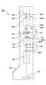
図1は、位相板を備えるTEM100を概略的に表している。 FIG. 1 schematically shows a
図1は、光軸102に沿った粒子ビーム−たとえば電子ビーム−を生成する粒子源104を示している。粒子は、典型的には80〜300keVの選択可能なエネルギーを有する。とはいえ、それよりも高いエネルギー(たとえば400keV〜1MeV)又はそれよりも低いエネルギー(たとえば50keV)が用いられても良い。粒子ビームは、試料ホルダ110と一緒になった状態で設けられる試料108に衝突する平行ビームを生成するように収束系106によって操作される。試料ホルダは、光軸に対して試料の位置を設定し、かつ、光軸に対して垂直な面内で試料を移動させ、かつ、前記光軸に対して試料を傾斜させて良い。対物レンズ112は、試料の拡大画像を生成する。対物レンズに続いて、対物レンズの後焦点面114の拡大画像を生成する拡大系116−たとえば二重レンズ−が設けられる。位相板118が、対物レンズの後焦点面の拡大画像内に設けられる。この共役面は、拡大系と投影系122との間に設けられる。位相板は、マニピュレータ120によって操作される。それにより光軸が位相板の中心に位置づけることが可能となる。投影系は、検出器124上に試料の拡大画像を生成する。それによりたとえば0.1nmの試料の詳細が明らかにされる。検出器は、蛍光スクリーン又はCCD若しくはCMOSカメラの形態をとって良い。たとえば蛍光スクリーンの場合、そのスクリーンはガラス窓126を介して視認されて良い。 FIG. 1 shows a
軸上での光学部品の位置合わせを行うため、TEMは、128-1…128-7で概略的に示されている多数の偏向器を有する。とはいえ他の場所では他の偏向器が含まれて良い。 In order to align the optical components on the axis, the TEM has a number of deflectors shown schematically at 128-1... 128-7. However, other deflectors may be included elsewhere.
位相板はまた後焦点面自身内に設けられても良いことに留意して欲しい。その場合、拡大系116は不要である。 Note that the phase plate may also be provided in the back focal plane itself. In that case, the
位相板は通常、ホルダ構造−たとえば電子顕微鏡において広く用いられているプラチナ製アパーチャ−によって取り囲まれる薄膜として形成される。係るアパーチャを備える位相板を形成することは、標準的なアパーチャホルダが、位相板の保持及び位置設定に用いられ得るという利点を有する。加熱されたアパーチャホルダが知られ、かつ、加熱は汚染を回避するのに用いられることに留意して欲しい。 The phase plate is usually formed as a thin film surrounded by a holder structure, such as a platinum aperture widely used in electron microscopes. Forming a phase plate with such an aperture has the advantage that a standard aperture holder can be used to hold and position the phase plate. Note that heated aperture holders are known and heating is used to avoid contamination.
ここで薄膜を、たとえば200keVの高線量の電子に曝露することによって、はじき出し損傷が起こる。その結果電子捕獲が起こる。これは、p型ドーパントと考えることができる。この結果生じる電子構造の変化−ここではGalvaniポテンシャルの変化と呼ばれる−は、外部ポテンシャルの局所的変化を引き起こす。 Here, by exposing the thin film to a high dose of electrons of, for example, 200 keV, spalling damage occurs. As a result, electron capture occurs. This can be considered a p-type dopant. The resulting change in electronic structure—referred to herein as the Galvani potential change—causes a local change in the external potential.
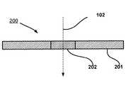
図2は、電子顕微鏡の軸102を取り囲む領域内で照射される薄膜200を概略的に示している。その結果、領域202の電子構造が変化する一方で、非照射領域201の電子構造は変化しない。 FIG. 2 schematically shows a
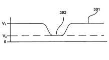
図3は、照射後における薄膜のポテンシャルを概略的に示している。軸から離れると、ポテンシャルは化学ポテンシャルに等しくなるが、照射領域はさらなる(負の)電子ポテンシャルを有する。 FIG. 3 schematically shows the potential of the thin film after irradiation. Off the axis, the potential is equal to the chemical potential, but the irradiated region has an additional (negative) electron potential.
V2がV1よりも小さいため、薄膜の照射部分202へ向かってその薄膜の照射部分202通り抜けて進行する非回折電子は、薄膜の他の部分を通り抜ける回折電子よりも加速されない。この結果、ビームが画像面内で干渉して画像を生成するとき、正の位相コントラストが生じる。Since V2 is smaller than V1, non-diffracted electrons traveling through the thin film irradiated
図4は、照射時間の関数として誘起される位相シフトを概略的に示している。 FIG. 4 schematically shows the phase shift induced as a function of irradiation time.
本願発明者等は、位相シフトが薄膜上に堆積される照射量の一次関数ではないことを発見した。このことは、電子ビームによって誘起されるGalvaniポテンシャルに上限が存在することを示唆している。本願発明者等はまた、より大きな領域(破線で示された直径125nmの照射領域)が、小さな領域(実線)と同一の合計ビーム電流を用いて照射されたときに、大きな領域では、小さな領域よりも大きな位相シフトが生じたことをも発見した。これは以下のように説明することができる。最初に最大の真空ポテンシャルが誘起されうると仮定する。続いて2つの電子ビーム同士を比較する。前記2つの電子ビームのうちの一は照射部分を通過し、かつ、前記2つの電子ビームのうちの他は前記照射部分から離れている。電子光学軸102に沿ってzが定義される。V(z)の-∞から+∞まで(より正確には試料面から画像面まで)の積分は、真空ポテンシャルに起因して異なる。照射されるスポットが成長するとき、2つの積分間での差異は、スポットのサイズに応じて変化する(ここでは同一の真空ポテンシャルであると仮定する)。従って位相シフトは、位相板の準備中に照射されるスポットのサイズを制御することによって調整されて良い。図4に示された曲線は同一のビーム電流で得られる。大きなスポットサイズを用いることによって実現可能なより高いビーム電流を用いる結果、設定時間が速くなることは、当業者には明らかである。 The inventors have discovered that phase shift is not a linear function of the dose deposited on the thin film. This suggests that there is an upper limit to the Galvani potential induced by the electron beam. The inventors have also stated that when a larger area (irradiated area with a diameter of 125 nm indicated by a broken line) is irradiated using the same total beam current as a smaller area (solid line), It was also discovered that a larger phase shift occurred. This can be explained as follows. Assume that the maximum vacuum potential can be induced first. Next, the two electron beams are compared. One of the two electron beams passes through the irradiated portion, and the other of the two electron beams is separated from the irradiated portion. Z is defined along the electro-
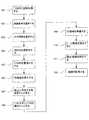
図5は、本発明による位相板を備えた透過型電子顕微鏡を動作させる手順を概略的に示している。 FIG. 5 schematically shows a procedure for operating a transmission electron microscope equipped with a phase plate according to the present invention.
段階501では、試料が透過型電子顕微鏡(TEM)内に供される。 In
段階502では、実験条件が選択される。前記実験条件には、電子ビームエネルギー、スポットサイズ収束アパーチャ(ビーム電流の選択を示唆する)、倍率等が含まれる。 In
段階503では、収束レンズが、試料に平行な電子ビームを照射するように設定される。 In
段階504では、試料がユーセントリック高さに設定され(このとき試料は高さを変化させることなく傾斜されうる)、かつ、焦点が設定される(その結果、試料面内の平行ビームが、対物レンズの後焦点面内で集束される)。 In
段階505では、標準的な顕微鏡の位置合わせが実行される。 In
段階506では、位相板がビーム経路内に挿入される。ここでは位相板は、その位相板の意図しない曝露(照射)を抑制するように挿入される。 In
任意の段階507では、面内に存在する条件(位相板が厳密に後焦点面内に存在するのか、又は、そこからわずかに離れているのかを示唆する)が、たとえば位相板を用いてチェックされ、かつ、必要であれば収束レンズが調節される。前述したように、わずかに面から外れるように動作させることによって、照射領域のサイズは調整/選択可能となる。位相板は後焦点面内に存在する必要はなく、その後焦点面に共役な面内に存在して良いことに留意して欲しい。 In
段階508では、ビームのピボット設定がチェックされ、かつ、たとえば位相板上の部位を用いた画像シフトが、対物レンズに入射するビームを傾斜させる結果、理想的に試料面内の純粋なシフト及び対物レンズの後焦点面(及びひいては位相板が存在する面)での純粋な傾斜となることを保証する。 In
段階509では、位相板が、(たとえばこれまでの実験に基づく)適切な合計期間位相板の清浄領域上にビームを保つことによって準備される。前記合計期間は、ビーム強度(ビーム電流)、ビームサイズ、及び位相板の材料に依存する。典型的にはこれは、10〜100秒の照射時間に達する。 In
段階510では、ビーム電流が、試料の撮像にとって通常の撮像条件にまで減少する。その後関心領域が試料上で特定される。 In
段階511では、画像が取得される。 In
前述したように、位相板は、汚染を回避するように(たとえば100℃〜400℃の制御された温度で)加熱された位相板であって良い。その場合、段階501はまた、位相板のドリフトを無視しうるように前記温度の熱的安定化をも含まなければならない。 As described above, the phase plate may be a heated phase plate (eg, at a controlled temperature of 100 ° C. to 400 ° C.) to avoid contamination. In that case, step 501 must also include thermal stabilization of the temperature so that phase plate drift can be ignored.
最終段階510と511は、試料から十分なデータが収集されるまで繰り返されて良い。試料の再集束及び(機械的な)シフトが必要であることも考えられる。
100 透過型電子顕微鏡
102 光軸
104 粒子源
106 収束系
108 試料
110 試料ホルダ
112 対物レンズ
114 後焦点面
116 拡大系
118 位相板
120 マニピュレータ
122 投影系
124 検出器
126 ガラス窓
128-1 偏向器
128-2 偏向器
128-3 偏向器
128-4 偏向器
128-5 偏向器
128-6 偏向器
128-7 偏向器
200 薄膜
201 非照射領域
202 照射領域
100 Transmission electron microscope
102 optical axis
104 Particle source
106 Convergence system
108 samples
110 Sample holder
112 Objective lens
114 Back focal plane
116 Expansion system
118 Phase plate
120 Manipulator
122 Projection system
124 detector
126 glass window
128-1 deflector
128-2 deflector
128-3 deflector
128-4 deflector
128-5 deflector
128-6 deflector
128-7 deflector
200 thin films
201 Non-irradiated area
202 Irradiation area
Claims (9)
Translated fromJapanese前記透過型電子顕微鏡内に前記位相板を導入する段階、
前記薄膜に集束電子ビームを照射することによって前記位相板を準備する段階、
前記透過型電子顕微鏡内に試料を導入する段階、及び、
前記の準備された位相板を用いて前記試料の画像を生成する段階、
を有し、
前記位相板を準備する段階が、前記薄膜の材料の除去をもたらさず、前記位相板に集束電子ビームを照射することによる前記薄膜の電子構造の変化の結果生じる真空ポテンシャルを局所的に発生させ、かつ、
前記真空ポテンシャルにより、前記薄膜の前記集束電子ビームが照射された部分を通り抜ける電子の絶対位相シフト|φ|が、前記集束電子ビームが照射されていない部分での値よりも小さくなり、
前記位相板を準備する段階において、汚染を回避するように前記位相板を加熱した状態とする、
ことを特徴とする方法。A method using a phase plate including a thin film in a transmission electron microscope,
Introducing the phase plate into the transmission electron microscope;
Providing the phase plate by irradiating the thin film with a focused electron beam;
Introducing a sample into the transmission electron microscope; and
Generating an image of the sampleusing the prepared phase plate;
Have
Providing the phase plate does not result in removal of the material of the thin film, but locally generates a vacuum potential resulting from a change in the electronic structure of the thin film by irradiating the phase plate with a focused electron beam; And,
Due to the vacuum potential, theabsolute phase shift| φ | of electrons passing throughthe portion irradiated with the focused electron beam of the thin film becomes smaller than the value at theportion not irradiated with the focused electron beam,
In the step ofpreparing the phase plate,and while heating the phase plate so as to avoid contamination,
A method characterized by that.
前記準備の後、前記位相板には、散乱電子と非散乱電子を含むビームが再度照射される、
請求項1に記載の方法。After irradiating the phase plate with a beam containing scattered electrons and non-scattered electrons, the mutual position of the phase plate and the beam is changed, and the phase plate is newly prepared,
After the preparation, the phase plate is again irradiated with a beam containing scattered electrons and non-scattered electrons.
The method of claim 1.
Applications Claiming Priority (6)
| Application Number | Priority Date | Filing Date | Title |
|---|---|---|---|
| EP13165356.0 | 2013-04-25 | ||
| EP13165356.0AEP2797100A1 (en) | 2013-04-25 | 2013-04-25 | Method of using a phase plate in a transmission electron microscope |
| EP13180361.1 | 2013-08-14 | ||
| EP13180361 | 2013-08-14 | ||
| EP13190405.4 | 2013-10-28 | ||
| EP13190405 | 2013-10-28 |
Publications (3)
| Publication Number | Publication Date |
|---|---|
| JP2014216319A JP2014216319A (en) | 2014-11-17 |
| JP2014216319A5 JP2014216319A5 (en) | 2017-05-18 |
| JP6286270B2true JP6286270B2 (en) | 2018-02-28 |
Family
ID=50489030
Family Applications (1)
| Application Number | Title | Priority Date | Filing Date |
|---|---|---|---|
| JP2014086240AActiveJP6286270B2 (en) | 2013-04-25 | 2014-04-18 | Method using a phase plate in a transmission electron microscope |
Country Status (4)
| Country | Link |
|---|---|
| US (1) | US9129774B2 (en) |
| EP (1) | EP2797101B1 (en) |
| JP (1) | JP6286270B2 (en) |
| CN (1) | CN104217910B (en) |
Families Citing this family (12)
| Publication number | Priority date | Publication date | Assignee | Title |
|---|---|---|---|---|
| DE102013019297A1 (en)* | 2013-11-19 | 2015-05-21 | Fei Company | Phase plate for a transmission electron microscope |
| EP2881970A1 (en) | 2013-12-04 | 2015-06-10 | Fei Company | Method of producing a freestanding thin film of nano-crystalline carbon |
| JP6418706B2 (en)* | 2014-07-30 | 2018-11-07 | フォルシュングスツェントルム・ユーリッヒ・ゲゼルシャフト・ミット・ベシュレンクテル・ハフツング | Adjustable ampere phase plate for charged particle imaging systems |
| EP3007201B1 (en) | 2014-10-08 | 2016-09-28 | Fei Company | Aligning a featureless thin film in a TEM |
| US10224175B2 (en)* | 2015-03-18 | 2019-03-05 | Battelle Memorial Institute | Compressive transmission microscopy |
| US10170274B2 (en)* | 2015-03-18 | 2019-01-01 | Battelle Memorial Institute | TEM phase contrast imaging with image plane phase grating |
| EP3104155A1 (en)* | 2015-06-09 | 2016-12-14 | FEI Company | Method of analyzing surface modification of a specimen in a charged-particle microscope |
| US10504695B2 (en) | 2015-12-25 | 2019-12-10 | Hitachi High-Technologies Corporation | Charged particle beam device and phase plate |
| US10580614B2 (en) | 2016-04-29 | 2020-03-03 | Battelle Memorial Institute | Compressive scanning spectroscopy |
| WO2018114299A1 (en) | 2016-12-19 | 2018-06-28 | Asml Netherlands B.V. | Charged particle beam inspection of ungrounded samples |
| US10295677B2 (en) | 2017-05-08 | 2019-05-21 | Battelle Memorial Institute | Systems and methods for data storage and retrieval |
| EP3474308A1 (en)* | 2017-10-17 | 2019-04-24 | Universiteit Antwerpen | Spatial phase manipulation of charged particle beam |
Family Cites Families (32)
| Publication number | Priority date | Publication date | Assignee | Title |
|---|---|---|---|---|
| US3908124A (en) | 1974-07-01 | 1975-09-23 | Us Energy | Phase contrast in high resolution electron microscopy |
| JPH067048A (en) | 1992-06-25 | 1994-01-18 | Masaki Ueno | Solution culture apparatus and raising seedling vessel to be used in the solution culture apparatus |
| US5814815A (en) | 1995-12-27 | 1998-09-29 | Hitachi, Ltd. | Phase-contrast electron microscope and phase plate therefor |
| JP2000268765A (en) | 1999-03-16 | 2000-09-29 | Jeol Ltd | Transmission electron microscope |
| JP2001084938A (en) | 1999-09-13 | 2001-03-30 | Hitachi Ltd | Transmission electron microscope and transmission electron microscope image observation method |
| JP3773389B2 (en) | 2000-03-27 | 2006-05-10 | 日本電子株式会社 | Thin film phase plate for phase contrast electron microscope, phase contrast electron microscope and phase plate antistatic method |
| JP3942363B2 (en) | 2001-02-09 | 2007-07-11 | 日本電子株式会社 | Lens system for phase plate of transmission electron microscope and transmission electron microscope |
| US6548810B2 (en) | 2001-08-01 | 2003-04-15 | The University Of Chicago | Scanning confocal electron microscope |
| JP4328044B2 (en) | 2001-09-25 | 2009-09-09 | 日本電子株式会社 | Differential contrast electron microscope and data processing method of electron microscope image |
| DE10200645A1 (en) | 2002-01-10 | 2003-07-24 | Leo Elektronenmikroskopie Gmbh | Electron microscope with circular illumination aperture |
| DE10206703A1 (en) | 2002-02-18 | 2003-08-28 | Max Planck Gesellschaft | Phase plate for electron microscopy and electron microscopic imaging |
| JP4254469B2 (en)* | 2003-05-23 | 2009-04-15 | 日本ビクター株式会社 | Optical pickup device and optical recording medium driving device |
| JP2005116365A (en) | 2003-10-08 | 2005-04-28 | Jeol Ltd | Transmission electron microscope with phase plate and phase plate lens system |
| US7737412B2 (en) | 2004-07-12 | 2010-06-15 | The Regents Of The University Of California | Electron microscope phase enhancement |
| JP4625317B2 (en) | 2004-12-03 | 2011-02-02 | ナガヤマ アイピー ホールディングス リミテッド ライアビリティ カンパニー | Phase plate for phase contrast electron microscope, method for producing the same, and phase contrast electron microscope |
| DE102005040267B4 (en) | 2005-08-24 | 2007-12-27 | Universität Karlsruhe | Method for producing a multilayer electrostatic lens arrangement, in particular a phase plate and such a phase plate |
| WO2007052723A1 (en) | 2005-11-04 | 2007-05-10 | Nagayama Ip Holdings, Llc | Phase plate for electron microscope, and its manufacturing method |
| JPWO2007058182A1 (en) | 2005-11-15 | 2009-04-30 | 大学共同利用機関法人自然科学研究機構 | Phase contrast electron microscope |
| DE102006011615A1 (en) | 2006-03-14 | 2007-09-20 | Carl Zeiss Nts Gmbh | Phase contrast electron microscope |
| DE102006055510B4 (en) | 2006-11-24 | 2009-05-07 | Ceos Corrected Electron Optical Systems Gmbh | Phase plate, image forming method and electron microscope |
| DE102007007923A1 (en) | 2007-02-14 | 2008-08-21 | Carl Zeiss Nts Gmbh | Phase-shifting element and particle beam device with phase-shifting element |
| EP2091062A1 (en) | 2008-02-13 | 2009-08-19 | FEI Company | TEM with aberration corrector and phase plate |
| GB0805819D0 (en) | 2008-03-31 | 2008-04-30 | Edgecombe Christopher | Phase plate for electron microscope |
| EP2131385A1 (en) | 2008-06-05 | 2009-12-09 | FEI Company | Hybrid phase plate |
| US7977633B2 (en) | 2008-08-27 | 2011-07-12 | Max-Planck-Gesellschaft Zur Foerderung Der Wissenschaften E. V. | Phase plate, in particular for an electron microscope |
| JP4896106B2 (en)* | 2008-09-30 | 2012-03-14 | 株式会社日立ハイテクノロジーズ | electronic microscope |
| WO2011071819A1 (en) | 2009-12-07 | 2011-06-16 | Regents Of The University Of California | Optical-cavity phase plate for transmission electron microscopy |
| US8785850B2 (en) | 2010-01-19 | 2014-07-22 | National Research Counsel Of Canada | Charging of a hole-free thin film phase plate |
| EP2400522A1 (en) | 2010-06-24 | 2011-12-28 | Fei Company | Blocking member for use in the diffraction plane of a TEM |
| EP2485239A1 (en) | 2011-02-07 | 2012-08-08 | FEI Company | Method for centering an optical element in a TEM comprising a contrast enhancing element |
| EP2667399A1 (en) | 2012-05-23 | 2013-11-27 | FEI Company | Improved phase plate for a TEM |
| EP2704178B1 (en) | 2012-08-30 | 2014-08-20 | Fei Company | Imaging a sample in a TEM equipped with a phase plate |
- 2014
- 2014-04-18JPJP2014086240Apatent/JP6286270B2/enactiveActive
- 2014-04-23EPEP14165529.0Apatent/EP2797101B1/enactiveActive
- 2014-04-25CNCN201410170093.2Apatent/CN104217910B/enactiveActive
- 2014-04-25USUS14/262,340patent/US9129774B2/enactiveActive
Also Published As
| Publication number | Publication date |
|---|---|
| CN104217910B (en) | 2017-09-12 |
| EP2797101A1 (en) | 2014-10-29 |
| US20140326876A1 (en) | 2014-11-06 |
| EP2797101B1 (en) | 2017-05-31 |
| CN104217910A (en) | 2014-12-17 |
| JP2014216319A (en) | 2014-11-17 |
| US9129774B2 (en) | 2015-09-08 |
Similar Documents
| Publication | Publication Date | Title |
|---|---|---|
| JP6286270B2 (en) | Method using a phase plate in a transmission electron microscope | |
| CN106645236B (en) | A kind of ultrafast transmission electron microscope system and using method thereof | |
| JP6262453B2 (en) | Method for preparation and visualization of flakes in a particle-optical device | |
| JP2009193963A (en) | Tem with aberration corrector and phase plate | |
| Egerton | Physical principles of electron microscopy | |
| JP6568646B2 (en) | electronic microscope | |
| Williams et al. | Electron microscopy of tobacco mosaic virus under conditions of minimal beam exposure | |
| JP2008270056A (en) | Scanning transmission electron microscope | |
| CN106711003B (en) | A kind of electronics source generating device and electron beam control method | |
| JP4826632B2 (en) | X-ray microscope and X-ray microscope method | |
| Egerton | An introduction to microscopy | |
| Egerton | The transmission electron microscope | |
| JP2020047589A (en) | Multi-electron beam imaging device with improved performance | |
| JPWO2014184881A1 (en) | Specimen holder and focused ion beam processing apparatus having the same | |
| JP7294971B2 (en) | Scanning electron microscope and secondary electron detection method for scanning electron microscope | |
| EP2797100A1 (en) | Method of using a phase plate in a transmission electron microscope | |
| JP2008204642A (en) | Scanning transmission charged particle beam equipment | |
| Plitzko et al. | Fundamentals of instrumentation and electron optics for cryo-electron tomography | |
| JPWO2018047228A1 (en) | Electron source and electron beam irradiation apparatus | |
| JP2007095576A (en) | Charged particle beam device and its focus control method | |
| JP6636061B2 (en) | Alignment of featureless thin film in TEM | |
| EP4625466A2 (en) | Heating assembly for charged particle beam system | |
| Cheng et al. | X-ray microradiography and shadow projection x-ray microscopy | |
| US20240355577A1 (en) | Charged-particle beam device for diffraction analysis | |
| WO2017109948A1 (en) | Charged particle beam apparatus and phase plate |
Legal Events
| Date | Code | Title | Description |
|---|---|---|---|
| A521 | Request for written amendment filed | Free format text:JAPANESE INTERMEDIATE CODE: A523 Effective date:20170328 | |
| A621 | Written request for application examination | Free format text:JAPANESE INTERMEDIATE CODE: A621 Effective date:20170328 | |
| A871 | Explanation of circumstances concerning accelerated examination | Free format text:JAPANESE INTERMEDIATE CODE: A871 Effective date:20170328 | |
| A975 | Report on accelerated examination | Free format text:JAPANESE INTERMEDIATE CODE: A971005 Effective date:20170418 | |
| A131 | Notification of reasons for refusal | Free format text:JAPANESE INTERMEDIATE CODE: A131 Effective date:20170425 | |
| A521 | Request for written amendment filed | Free format text:JAPANESE INTERMEDIATE CODE: A523 Effective date:20170712 | |
| A131 | Notification of reasons for refusal | Free format text:JAPANESE INTERMEDIATE CODE: A131 Effective date:20170801 | |
| A521 | Request for written amendment filed | Free format text:JAPANESE INTERMEDIATE CODE: A523 Effective date:20171026 | |
| TRDD | Decision of grant or rejection written | ||
| A01 | Written decision to grant a patent or to grant a registration (utility model) | Free format text:JAPANESE INTERMEDIATE CODE: A01 Effective date:20180109 | |
| A61 | First payment of annual fees (during grant procedure) | Free format text:JAPANESE INTERMEDIATE CODE: A61 Effective date:20180205 | |
| R150 | Certificate of patent or registration of utility model | Ref document number:6286270 Country of ref document:JP Free format text:JAPANESE INTERMEDIATE CODE: R150 | |
| R250 | Receipt of annual fees | Free format text:JAPANESE INTERMEDIATE CODE: R250 | |
| R250 | Receipt of annual fees | Free format text:JAPANESE INTERMEDIATE CODE: R250 | |
| R250 | Receipt of annual fees | Free format text:JAPANESE INTERMEDIATE CODE: R250 | |
| R250 | Receipt of annual fees | Free format text:JAPANESE INTERMEDIATE CODE: R250 | |
| R250 | Receipt of annual fees | Free format text:JAPANESE INTERMEDIATE CODE: R250 |