JP6285662B2 - Variable optical retarder - Google Patents
Variable optical retarderDownload PDFInfo
- Publication number
- JP6285662B2 JP6285662B2JP2013170918AJP2013170918AJP6285662B2JP 6285662 B2JP6285662 B2JP 6285662B2JP 2013170918 AJP2013170918 AJP 2013170918AJP 2013170918 AJP2013170918 AJP 2013170918AJP 6285662 B2JP6285662 B2JP 6285662B2
- Authority
- JP
- Japan
- Prior art keywords
- liquid crystal
- crystal layer
- sub
- grating
- variable optical
- Prior art date
- Legal status (The legal status is an assumption and is not a legal conclusion. Google has not performed a legal analysis and makes no representation as to the accuracy of the status listed.)
- Active
Links
- 230000003287optical effectEffects0.000titleclaimsdescription107
- 239000004973liquid crystal related substanceSubstances0.000claimsdescription115
- 239000000758substrateSubstances0.000claimsdescription26
- 230000010287polarizationEffects0.000claimsdescription25
- 230000005684electric fieldEffects0.000claimsdescription16
- 230000001902propagating effectEffects0.000claimsdescription15
- 229910052710siliconInorganic materials0.000claimsdescription11
- 239000010703siliconSubstances0.000claimsdescription11
- VYPSYNLAJGMNEJ-UHFFFAOYSA-NSilicium dioxideChemical compoundO=[Si]=OVYPSYNLAJGMNEJ-UHFFFAOYSA-N0.000claimsdescription10
- 230000001154acute effectEffects0.000claimsdescription10
- XUIMIQQOPSSXEZ-UHFFFAOYSA-NSiliconChemical compound[Si]XUIMIQQOPSSXEZ-UHFFFAOYSA-N0.000claimsdescription9
- 238000000034methodMethods0.000claimsdescription9
- 229910052751metalInorganic materials0.000claimsdescription8
- 239000002184metalSubstances0.000claimsdescription8
- 230000035945sensitivityEffects0.000claimsdescription7
- 239000004065semiconductorSubstances0.000claimsdescription5
- 235000012239silicon dioxideNutrition0.000claimsdescription5
- 239000000377silicon dioxideSubstances0.000claimsdescription5
- 230000005540biological transmissionEffects0.000claimsdescription4
- 230000001737promoting effectEffects0.000claimsdescription3
- 230000000644propagated effectEffects0.000claimsdescription2
- -1tantalaChemical compound0.000claims1
- 239000010410layerSubstances0.000description54
- 210000002858crystal cellAnatomy0.000description14
- 239000011248coating agentSubstances0.000description3
- 238000000576coating methodMethods0.000description3
- 238000002310reflectometryMethods0.000description3
- 230000002441reversible effectEffects0.000description3
- 229910004298SiO 2Inorganic materials0.000description2
- 229910052782aluminiumInorganic materials0.000description2
- XAGFODPZIPBFFR-UHFFFAOYSA-NaluminiumChemical compound[Al]XAGFODPZIPBFFR-UHFFFAOYSA-N0.000description2
- 230000007423decreaseEffects0.000description2
- 230000003111delayed effectEffects0.000description2
- 230000001419dependent effectEffects0.000description2
- 238000010586diagramMethods0.000description2
- 230000000694effectsEffects0.000description2
- 239000012530fluidSubstances0.000description2
- 238000003780insertionMethods0.000description2
- 230000037431insertionEffects0.000description2
- 239000000463materialSubstances0.000description2
- 238000012986modificationMethods0.000description2
- 230000004048modificationEffects0.000description2
- 230000010363phase shiftEffects0.000description2
- 229910052715tantalumInorganic materials0.000description2
- GUVRBAGPIYLISA-UHFFFAOYSA-Ntantalum atomChemical compound[Ta]GUVRBAGPIYLISA-UHFFFAOYSA-N0.000description2
- 230000004075alterationEffects0.000description1
- 210000004027cellAnatomy0.000description1
- 239000011247coating layerSubstances0.000description1
- 239000013256coordination polymerSubstances0.000description1
- 229910003460diamondInorganic materials0.000description1
- 239000010432diamondSubstances0.000description1
- 239000011521glassSubstances0.000description1
- AMGQUBHHOARCQH-UHFFFAOYSA-Nindium;oxotinChemical compound[In].[Sn]=OAMGQUBHHOARCQH-UHFFFAOYSA-N0.000description1
- 239000007788liquidSubstances0.000description1
- 239000012528membraneSubstances0.000description1
- 230000000737periodic effectEffects0.000description1
Images


Classifications
- G—PHYSICS
- G02—OPTICS
- G02F—OPTICAL DEVICES OR ARRANGEMENTS FOR THE CONTROL OF LIGHT BY MODIFICATION OF THE OPTICAL PROPERTIES OF THE MEDIA OF THE ELEMENTS INVOLVED THEREIN; NON-LINEAR OPTICS; FREQUENCY-CHANGING OF LIGHT; OPTICAL LOGIC ELEMENTS; OPTICAL ANALOGUE/DIGITAL CONVERTERS
- G02F1/00—Devices or arrangements for the control of the intensity, colour, phase, polarisation or direction of light arriving from an independent light source, e.g. switching, gating or modulating; Non-linear optics
- G02F1/01—Devices or arrangements for the control of the intensity, colour, phase, polarisation or direction of light arriving from an independent light source, e.g. switching, gating or modulating; Non-linear optics for the control of the intensity, phase, polarisation or colour
- G02F1/13—Devices or arrangements for the control of the intensity, colour, phase, polarisation or direction of light arriving from an independent light source, e.g. switching, gating or modulating; Non-linear optics for the control of the intensity, phase, polarisation or colour based on liquid crystals, e.g. single liquid crystal display cells
- G02F1/133—Constructional arrangements; Operation of liquid crystal cells; Circuit arrangements
- G02F1/1333—Constructional arrangements; Manufacturing methods
- G02F1/1335—Structural association of cells with optical devices, e.g. polarisers or reflectors
- G—PHYSICS
- G02—OPTICS
- G02B—OPTICAL ELEMENTS, SYSTEMS OR APPARATUS
- G02B5/00—Optical elements other than lenses
- G02B5/30—Polarising elements
- G02B5/3083—Birefringent or phase retarding elements
- G—PHYSICS
- G02—OPTICS
- G02B—OPTICAL ELEMENTS, SYSTEMS OR APPARATUS
- G02B5/00—Optical elements other than lenses
- G02B5/32—Holograms used as optical elements
- G—PHYSICS
- G02—OPTICS
- G02F—OPTICAL DEVICES OR ARRANGEMENTS FOR THE CONTROL OF LIGHT BY MODIFICATION OF THE OPTICAL PROPERTIES OF THE MEDIA OF THE ELEMENTS INVOLVED THEREIN; NON-LINEAR OPTICS; FREQUENCY-CHANGING OF LIGHT; OPTICAL LOGIC ELEMENTS; OPTICAL ANALOGUE/DIGITAL CONVERTERS
- G02F1/00—Devices or arrangements for the control of the intensity, colour, phase, polarisation or direction of light arriving from an independent light source, e.g. switching, gating or modulating; Non-linear optics
- G02F1/01—Devices or arrangements for the control of the intensity, colour, phase, polarisation or direction of light arriving from an independent light source, e.g. switching, gating or modulating; Non-linear optics for the control of the intensity, phase, polarisation or colour
- G02F1/13—Devices or arrangements for the control of the intensity, colour, phase, polarisation or direction of light arriving from an independent light source, e.g. switching, gating or modulating; Non-linear optics for the control of the intensity, phase, polarisation or colour based on liquid crystals, e.g. single liquid crystal display cells
- G02F1/133—Constructional arrangements; Operation of liquid crystal cells; Circuit arrangements
- G02F1/1333—Constructional arrangements; Manufacturing methods
- G02F1/1335—Structural association of cells with optical devices, e.g. polarisers or reflectors
- G02F1/133504—Diffusing, scattering, diffracting elements
- G—PHYSICS
- G02—OPTICS
- G02F—OPTICAL DEVICES OR ARRANGEMENTS FOR THE CONTROL OF LIGHT BY MODIFICATION OF THE OPTICAL PROPERTIES OF THE MEDIA OF THE ELEMENTS INVOLVED THEREIN; NON-LINEAR OPTICS; FREQUENCY-CHANGING OF LIGHT; OPTICAL LOGIC ELEMENTS; OPTICAL ANALOGUE/DIGITAL CONVERTERS
- G02F1/00—Devices or arrangements for the control of the intensity, colour, phase, polarisation or direction of light arriving from an independent light source, e.g. switching, gating or modulating; Non-linear optics
- G02F1/01—Devices or arrangements for the control of the intensity, colour, phase, polarisation or direction of light arriving from an independent light source, e.g. switching, gating or modulating; Non-linear optics for the control of the intensity, phase, polarisation or colour
- G02F1/15—Devices or arrangements for the control of the intensity, colour, phase, polarisation or direction of light arriving from an independent light source, e.g. switching, gating or modulating; Non-linear optics for the control of the intensity, phase, polarisation or colour based on an electrochromic effect
- G02F1/153—Constructional details
- G02F1/1533—Constructional details structural features not otherwise provided for
- G—PHYSICS
- G02—OPTICS
- G02F—OPTICAL DEVICES OR ARRANGEMENTS FOR THE CONTROL OF LIGHT BY MODIFICATION OF THE OPTICAL PROPERTIES OF THE MEDIA OF THE ELEMENTS INVOLVED THEREIN; NON-LINEAR OPTICS; FREQUENCY-CHANGING OF LIGHT; OPTICAL LOGIC ELEMENTS; OPTICAL ANALOGUE/DIGITAL CONVERTERS
- G02F2201/00—Constructional arrangements not provided for in groups G02F1/00 - G02F7/00
- G02F2201/30—Constructional arrangements not provided for in groups G02F1/00 - G02F7/00 grating
- G02F2201/307—Reflective grating, i.e. Bragg grating
Landscapes
- Physics & Mathematics (AREA)
- Nonlinear Science (AREA)
- General Physics & Mathematics (AREA)
- Optics & Photonics (AREA)
- Mathematical Physics (AREA)
- Chemical & Material Sciences (AREA)
- Crystallography & Structural Chemistry (AREA)
- Liquid Crystal (AREA)
- Polarising Elements (AREA)
Description
Translated fromJapanese本発明は、光学リターダに関し、さらに詳細には、光ビームに可変位相遅延を与える可変光学リターダに関する。 The present invention relates to an optical retarder, and more particularly to a variable optical retarder that provides a variable phase delay to a light beam.
液晶可変光学リターダは、可変光学位相遅延を与え、および/または光ビームの偏光状態を変化させるために使用される。通常の液晶可変光学リターダでは、2つの透明電極の間に、数マイクロメートルの厚さの液晶流体層が挟まれている。液晶分子は、異方性が高いので、電極に電圧が印加されると、電極間に生じる電界によって配向される。液晶分子の電界誘起配向によって、液晶層の有効屈折率が変化し、これが、液晶層内を伝搬する光ビームの光学位相に影響を及ぼす。「ディレクタ」と呼ばれる液晶分子の主配向方向に対して光ビームが45度の角度で直線偏光すると、誘起された光学位相差によって光ビームの偏光状態が変化する可能性がある。例えば、直線光学偏光が回転する可能性がある。光ビームが液晶分子の主配向方向に沿って直線偏光すると、可変光学リターダによって光ビームに可変光学位相遅延が与えられる。 Liquid crystal variable optical retarders are used to provide variable optical phase delay and / or change the polarization state of the light beam. In a normal liquid crystal variable optical retarder, a liquid crystal fluid layer having a thickness of several micrometers is sandwiched between two transparent electrodes. Since the liquid crystal molecules have high anisotropy, when a voltage is applied to the electrodes, the liquid crystal molecules are aligned by an electric field generated between the electrodes. The effective refractive index of the liquid crystal layer changes due to the electric field induced orientation of the liquid crystal molecules, which affects the optical phase of the light beam propagating in the liquid crystal layer. If the light beam is linearly polarized at an angle of 45 degrees with respect to the main alignment direction of the liquid crystal molecules called “director”, the polarization state of the light beam may change due to the induced optical phase difference. For example, linear optical polarization may rotate. When the light beam is linearly polarized along the main alignment direction of the liquid crystal molecules, the variable optical retarder imparts a variable optical phase delay to the light beam.
複数の可変光学リターダのアレイは、共通の液晶層の下に個別制御可能なピクセルのアレイを配列することによって構築することができる。直線偏光した光ビームがこのようなアレイを照らすと、このビームに所定の光学位相パターンが与えられ、可動部分がなくても光ビームの多様な合焦またはステアリングを行うことができる。可変光学リターダのアレイには、ビーム走査/ステアリングや光学収差補正などの分野で様々に応用されている。 An array of multiple variable optical retarders can be constructed by arranging an array of individually controllable pixels under a common liquid crystal layer. When a linearly polarized light beam illuminates such an array, the beam is given a predetermined optical phase pattern, and the light beam can be variously focused or steered without moving parts. The array of variable optical retarders has various applications in fields such as beam scanning / steering and optical aberration correction.
液晶可変リターダの欠点の1つは、通常、適切に動作するためには偏光した光ビームが必要であることである。ただし、この欠点は本質的なものではなく、適当な偏波ダイバーシチ構成を用いることによって克服することができる。例えば、G.D.Loveは、Appl.Opt.、Vol.32、No.13、p.2222〜2223、1993年5月1日の「非偏光光の液晶位相変調器」と題する論文において、反射偏光無依存型可変光学リターダを開示している。図1を参照すると、Loveの可変光学リターダ10は、液晶セル12とミラー13の間に配置された4分の1波長板(QWP)11を有する。動作に際しては、入来する垂直直線偏光(V−LP)光ビーム14が、液晶セル12および4分の1波長板11を通って伝搬し、ミラー13で反射されて、4分の1波長板11および液晶セル12を逆方向に通って伝搬する。反射光ビームは、16に示してある。液晶セル12は、垂直に配向されたディレクタ15を有する。したがって、可変光学位相遅延は、第1の光路では、光ビーム14の偏光状態を変化させることなく光ビーム14に与えられる。4分の1波長板11は、垂直偏光状態を左円偏光(LH−CP)に変化させるように配向される。この左円偏光は、ミラー13による反射後は右円偏光(RH−CP)になる。第2の光路では、4分の1波長板11は、右円偏光を水平直線偏光(H−LP)に変化させるが、ディレクタ15が水平直線偏光に対して直交するように配向されている、すなわち垂直に配向されているので、この水平直線偏光は液晶セル12によって変化しない。入来する光ビーム14が水平偏光している場合(分かりやすくするために図示しない)には、光ビーム14は、液晶セル12を通る第1の光路ではなく第2の光路で垂直偏光され、同じ量だけ位相遅延されることが分かる。したがって、光ビーム14が偏光していない、またはランダムに偏光されている場合には、光ビーム14は、その偏光状態に関わりなく、同じ量だけ位相遅延される。したがって、可変光学リターダ10は、偏光無依存型である。 One disadvantage of liquid crystal variable retarders is that a polarized light beam is usually required to operate properly. However, this drawback is not essential and can be overcome by using an appropriate polarization diversity configuration. For example, G. D. Love is described in Appl. Opt. Vol. 32, no. 13, p. 2222-2223, May 1, 1993, entitled "Non-Polarized Liquid Crystal Phase Modulator" discloses a reflective polarization independent variable optical retarder. Referring to FIG. 1, Love's variable
図1の可変光学リターダ10の欠点の1つは、液晶セル12とミラー13の間に4分の1波長板11を配置することにより、ミラー13と液晶セル12の間の距離Dが大きくなることである。これは、入来する光ビーム14が距離Dを伝搬する間に発散するので、好ましくない。ビームが発散することにより、液晶セル12上のビーム・スポット・サイズが大きくなる。ビーム・スポット・サイズが大きくなると、空間解像度が低下するので、液晶セル12がピクセル化されている可変リターダ・アレイ構成では好ましくない。 One of the disadvantages of the variable
可変光学リターダ10の別の欠点は、外部の4分の1波長板11に対応するためには、液晶セル12が透過性でなければならないことである。透過性の液晶セルは、通常、複光路構成となり、単光路構成の反射性液晶セルよりも光損失が大きくなる。これは、透過性セルでは、入来する光が2つの透明電極を2回通過しなければならないからである。透明電極は、導電性と光透過性の両方を有していなければならない。これらの要件には、それぞれ相容れない部分もあるので、通常は、透明電極によって、ある程度余計な光損失がシステムに導入されることになる。 Another disadvantage of the variable
James他は、J.Opt.Soc.Am.A、Vol.24、No.8、p.2464〜2473の「再構成可能なビーム・ステアリングのための液晶2D空間光変調器の回折効率および偏光感度のモデリング」と題する論文において、電極の1つが高い反射性を有し、4分の1反射板が液晶セルの内部に配置される、反射性偏光無依存液晶リターダ・アレイを開示している。この場合に生じる光損失は低い。これは、Jamesの装置では、入来する光ビームが2回通過する電極が2つではなく1つだからである。ただし、4分の1波長板を内部に配置することにより、液晶層の両端間の電界が弱くなるので、この電界減少を補償するためにより高い駆動電圧が必要となる。 James et al. Opt. Soc. Am. A, Vol. 24, no. 8, p. In a paper titled “Diffraction Efficiency and Polarization Sensitivity of Liquid Crystal 2D Spatial Light Modulator for Reconfigurable Beam Steering” 2464-2473, one of the electrodes has a high reflectivity A reflective polarization independent liquid crystal retarder array is disclosed in which a reflector is disposed within the liquid crystal cell. The optical loss that occurs in this case is low. This is because in James's apparatus, the incoming light beam passes through only one electrode instead of two. However, since the electric field between both ends of the liquid crystal layer is weakened by arranging the quarter-wave plate inside, a higher driving voltage is required to compensate for this electric field decrease.
本発明の目的は、過剰な光損失または駆動電圧損失を生じることなく偏光感度を低下させた可変光学リターダを提供することである。 It is an object of the present invention to provide a variable optical retarder with reduced polarization sensitivity without causing excessive light loss or drive voltage loss.
本発明によれば、電極と液晶層の間の液晶可変光学リターダの内部に、誘電体または半導体のサブ波長格子(sub−wavelength grating)が配置される。サブ波長格子は、極めて薄い厚さでありながら4分の1波長板として作用するので、サブ波長格子を内部に配置することによる駆動電圧損失が軽減される。サブ波長格子は、高い反射性を有するようにすることもできる。例えば、サブ波長格子は、金属反射体と比較してさらに光損失を低下させる、多層誘電体高反射体を含むことができる。 According to the present invention, a dielectric or semiconductor sub-wavelength grating is disposed inside the liquid crystal variable optical retarder between the electrode and the liquid crystal layer. The sub-wavelength grating functions as a quarter-wave plate while having an extremely thin thickness, so that the driving voltage loss due to the sub-wavelength grating being disposed inside is reduced. The subwavelength grating can also be made highly reflective. For example, the sub-wavelength grating can include a multilayer dielectric high reflector that further reduces optical loss compared to a metal reflector.
本発明の1つの態様によれば、
第1の連続的な板状電極と、
前記第1の電極に対向する、第2の実質的に透明な連続的な板状電極と、
前記第1の電極と前記第2の電極の間に電圧が印加されたときに前記第2の電極に入射する光に可変光学位相シフトを与える、前記第1の電極と前記第2の電極の間に配置され、ディレクタを有する液晶層と、
前記液晶層と前記第1の電極の間に配置され、前記ディレクタに対して鋭角をなす、好ましくは45度をなす、格子線を有するサブ波長格子とを含む、液晶可変光学リターダが提供される。According to one aspect of the invention,
A first continuous plate electrode;
A second substantially transparent continuous plate electrode opposite the first electrode;
The first electrode and the second electrode are configured to apply a variable optical phase shift to light incident on the second electrode when a voltage is applied between the first electrode and the second electrode. A liquid crystal layer disposed between and having a director;
A liquid crystal tunable optical retarder is provided that is disposed between the liquid crystal layer and the first electrode and includes a sub-wavelength grating having a grating line, which forms an acute angle with respect to the director, preferably 45 degrees. .
本発明によれば、さらに、
入射する光ビームに可変位相遅延を与える可変光学リターダであって、
ピクセル電極を有する基板と、
入射する光ビームに第1の光学位相差を与える、前記ピクセル電極上に配置され、かつ前記ピクセル電極から分離したサブ波長格子であり、互いに平行に延びる複数の格子線を有するサブ波長格子と、
内部を伝搬する光ビームに第2の光学位相差を与える、前記サブ波長格子上の液晶層と、
前記液晶層上の実質的に透明な背面電極とを含み、
前記ピクセル電極と前記背面電極の間に電圧が印加されたときに前記第2の光学位相差が変化することにより、前記液晶層を通って伝搬する光ビームに可変位相遅延を与え、
前記液晶層のディレクタが、前記格子線に対して鋭角をなすことにより、前記可変光学リターダの前記光ビームの偏光状態に対する感度が低下する、可変光学リターダが提供される。According to the invention,
A variable optical retarder that provides a variable phase delay to an incident light beam,
A substrate having pixel electrodes;
A sub-wavelength grating that provides a first optical phase difference to an incident light beam, the sub-wavelength grating being disposed on the pixel electrode and separated from the pixel electrode, and having a plurality of grating lines extending in parallel to each other;
A liquid crystal layer on the sub-wavelength grating that provides a second optical phase difference to the light beam propagating therein;
A substantially transparent back electrode on the liquid crystal layer,
Providing a variable phase delay to the light beam propagating through the liquid crystal layer by changing the second optical phase difference when a voltage is applied between the pixel electrode and the back electrode;
A variable optical retarder is provided in which the director of the liquid crystal layer makes an acute angle with respect to the lattice lines, thereby reducing the sensitivity of the variable optical retarder to the polarization state of the light beam.
本発明の別の態様によれば、さらに、トリム・リターダを含む液晶オン・シリコン(liquid‐crystal‐on‐silicon)空間光変調器であって、前記トリム・リターダがサブ波長格子を含む、液晶オン・シリコン空間光変調器が提供される。 According to another aspect of the present invention, there is further provided a liquid crystal-on-silicon spatial light modulator including a trim retarder, wherein the trim retarder includes a sub-wavelength grating. An on-silicon spatial light modulator is provided.
本発明のさらに別の態様によれば、さらに、
光ビームに可変位相遅延を与える方法であって、
(a)前記ビームを液晶層を通して伝搬させ、次いで前記液晶層のディレクタに対して鋭角をなすように配向された格子線を有するサブ波長格子を通して伝搬させるステップと、
(b)ステップ(a)で伝搬したビームを反射して、前記液晶層を逆に通して伝搬させるステップと、
(c)ステップ(a)および(b)を実行しながら、前記液晶層および前記サブ波長格子の外部にある、前記液晶層および前記サブ波長格子と平行な1対の板状電極を介して前記液晶層に電界を印加して、前記液晶層の光学位相差を変化させることにより、前記光ビームの位相遅延を変化させるステップとを含み、前記電極の平坦性により、前記印加電界の空間的均一性が促進され、それにより前記液晶層の前記変化後の光学位相差の空間的均一性が促進される、方法が提供される。According to yet another aspect of the invention,
A method of providing a variable phase delay to a light beam,
(A) propagating the beam through a liquid crystal layer and then propagating through a sub-wavelength grating having grating lines oriented at an acute angle to the director of the liquid crystal layer;
(B) reflecting the beam propagated in step (a) and propagating through the liquid crystal layer in reverse;
(C) While performing steps (a) and (b), the liquid crystal layer and the sub-wavelength grating, which are outside the liquid crystal layer and the sub-wavelength grating, through a pair of plate-like electrodes, Applying an electric field to the liquid crystal layer to change an optical phase difference of the liquid crystal layer, thereby changing a phase delay of the light beam, and applying the spatial uniformity of the applied electric field due to the flatness of the electrode. A method is provided in which the properties are promoted, thereby promoting the spatial uniformity of the optical phase difference after the change of the liquid crystal layer.
好ましい実施形態によれば、前記サブ波長格子はいかなる金属も含まず、これにより、光損失および電界フリンジ効果または遮蔽効果が低減する。 According to a preferred embodiment, the subwavelength grating does not contain any metal, thereby reducing light loss and field fringing or shielding effects.
以下、図面と関連付けて例示的な実施形態について説明する。 Hereinafter, exemplary embodiments will be described in association with the drawings.
様々な実施形態および実施例に関連付けて本発明の教示について説明するが、この説明は、本発明の教示をこれらの実施形態に限定するものではない。本発明の教示は、これらの実施形態に限定されるのではなく、様々な代替形態、修正形態および均等物を包含するものであることを、当業者なら理解するであろう。図2A、2B、3A、3Bおよび3Cでは、同じ参照番号は同じ要素を示している。 While the teachings of the present invention will be described in connection with various embodiments and examples, this description is not intended to limit the teachings of the invention to these embodiments. Those skilled in the art will appreciate that the teachings of the present invention are not limited to these embodiments, but include various alternatives, modifications and equivalents. In FIGS. 2A, 2B, 3A, 3B and 3C, the same reference numbers indicate the same elements.
図2Aおよび図2Bを参照すると、本発明の可変光学リターダ20は、第1の連続的な板状電極21および第1の電極21に対向する第2の実質的に透明な連続的な板状電極22と、液晶層26と、液晶層26と第1の電極21の間に配置されるサブ波長格子24とを含む。図2Bから分かるように、サブ波長格子24は、互いに平行に延びる複数の格子線25を有する。液晶層26のディレクタ27は、格子線25に対して45度の角度αをなす。サブ波長格子24は、1回透過で4分の1波長の位相差を与えるので、2回透過では2分の1波長の位相差になる。 2A and 2B, the variable
動作に際しては、光ビーム28は、第2の電極22を通して液晶層26に入射する。第1の電極21と第2の電極22の間に電圧Vを印加することにより、液晶層26の光学位相差を変化させる。その結果として、可変位相遅延が、光ビーム28に与えられる。サブ波長格子24は、ディレクタ27に対してα=45度の角度で配向された4分の1波長板として作用して、図1に関連して上記で説明したように水平偏光と垂直偏光を切り替え、これにより、可変光学リターダ20の光ビーム28の偏光状態に対する感度を低下させる。実施形態によっては、角度αは45度に等しくなく、鋭角のままである。ある程度の偏光依存性が必要な場合には、サブ波長格子24の位相差の値を、1回透過の4分の1波長からずらしてもよい。 In operation, the
例えば0.2ミクロン以内または好ましくは0.1ミクロン以内の平坦度を有するような第1の電極21の上面23の平坦かつ一様な表面23は、例えばサブ波長格子24を第1の電極21に直接微細加工した場合に第1の電極21が有する波形表面よりもより一様な電界を生成するので、第1の電極21の上面23が平坦かつ一様であることは有利である。より一様な電界を液晶層26に印加することにより、より一様な液晶層26の光学位相差プロフィルを生じ、それにより、フリンジ電界によって乱される液晶層26の不要かつ制御不能な回折効果を低減する。 For example, the flat and
第1の電極21の上面23は、高い反射性を有するようにすることができ、この場合、サブ波長格子24は透過性にする。ただし、サブ波長格子24自体が高い反射性を有するようにしてもよい。例えば、サブ波長格子24が、多層誘電体高反射体(図示せず)を含み、第1の電極21の表面23が高い反射率を有する必要がないようにしてもよい。金属反射体は、必然的にある程度の光損失を引き起こすので、サブ波長格子24の誘電体高反射体は、第1の電極21の表面23より高い反射率を有することができ、その結果、可変光学リターダ20の全体的な光損失を低減することができる。光損失をさらに低減し、電界遮蔽を防止するために、サブ波長格子24は、いかなる金属も含まない誘電体または半導体で構成することが好ましい。例えば、サブ波長格子24は、二酸化シリコン(SiO2)のホスト内にタンタラ(Ta2O5)またはシリコン(Si)の周期構造を含むことができる。The
図3Aおよび図3Bを参照すると、本発明の可変光学リターダ30は、複数のピクセル電極31が形成された基板34Cと、ピクセル電極31上に配置され、かつピクセル電極31から分離したサブ波長格子34と、サブ波長格子34上の液晶層36と、液晶層36上の実質的に透明の背面電極32とを含む。ガラス・カバー・プレート39が、インジウムスズ酸化物(ITO)などの適当な材料で構成された背面電極32を支持している。カバー・プレート39は、反射防止(AR)被膜39Aを有する。サブ波長格子34および背面電極32に接着された配向層37は、液晶層36内の液晶分子を整列させるために使用される。サブ波長格子34は、リッジ34Aの形状をした複数の格子線を有する。液晶層36は、リッジ34Aの間の隙間34Bの中にも延在している。図示の実施形態では、基板34Cは、二酸化シリコン基板である。 3A and 3B, the variable
動作に際しては、光ビーム38は、AR被膜39A、カバー・プレート39、透明背面電極32および液晶層36を順に通って伝搬し、サブ波長格子34に入射し、ピクセル電極31の上面33で反射されて、上記の積層構造を逆の順序で通って伝搬する。液晶層36およびサブ波長格子34は、第1の光学位相差および第2の光学位相差をそれぞれ光ビーム38に与える。ピクセル電極31と背面電極32の間に電圧が印加され、液晶層36を通って伝搬する光ビーム38に可変位相遅延が与えられると、第2の光学位相差は変化する。液晶層36のディレクタ(図示せず)は、格子線34Aに対して45度の角度をなすので、可変光学リターダ30の光ビーム38の偏光状態に対する感度は低減される。 In operation, the
上述のように、フリンジ電界と、これに付随する液晶の屈折率の空間変調とを回避するために、ピクセル電極31の上面33は平坦であることが好ましい。反射率を高めるために、サブ波長格子34を反射性にしてもよい。また、1実施形態では、液晶層36のディレクタは、格子線(リッジ34A)に対して鋭角をなし、必ずしも45度に等しい角度にはならない。三角形や台形など、方形リッジ34A以外の格子線の形状を使用することもできる。サブ波長格子34は、1回透過で4分の1波長の光学位相差を有することが好ましい。すなわち、図3Aで光ビーム38が下向きに伝搬するときに4分の1波長の位相差があり、光ビーム38が反射されて上方に伝搬するときに4分の1波長の位相差があることが好ましい。図2の可変光学リターダ20に関連して上記で説明したように、図3Aの可変光学リターダ30のサブ波長格子34は、誘電体または半導体を含むことが好ましく、光損失を少なくし、ピクセル電極31と背面電極32とが生成する電界の乱れを少なくするためには、いかなる金属も含まない純粋な誘電体であることが最も好ましい。非限定的な例としては、サブ波長格子34の格子線またはリッジ34Aは、タンタラ(Ta2O5)で構成することができる。As described above, the
図3Cに示す可変光学リターダ30の実施形態では、タンタラ(tantala)のリッジ34Aが二酸化シリコン基板34C内に形成されることで、サブ波長格子34が平坦化されるので、下側配向層37が平坦になり、したがって、液晶層36の両側が平坦になる。これにより、図3Bに示すように一部が液晶材料で構成されるサブ波長格子構造を有さないので、より安定なサブ波長格子34が得られる。 In the embodiment of the variable
図3Aから図3Cでは、共通の液晶層36、サブ波長格子34および背面電極32の下に複数のピクセル電極31を示しているが、可変光学リターダ30は、ピクセル電極31を1つしか含まないようにして、実質的に、光ビーム38全体に同じ可変光学位相シフトを与える必要がある分野で使用することができる非ピクセル化光学リターダとすることもできることを理解されたい。 3A to 3C show a plurality of
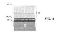
図3Aから図3Cのピクセル化可変光学リターダ30は、液晶オン・シリコン(LCoS)技術で実装することができるので有利である。図4を参照すると、LCoS可変光学リターダ40が示してある。LCoS可変光学リターダ40では、二酸化シリコン基板34Cは、複数のピクセル電極31の下に位置して各ピクセル電極31に独立して電圧を印加するドライバ回路41をその上に有する、シリコン基板42上の被覆層である。シリコン・ドライバ・エレクトロニクス41は、小型で高速にすることができ、極めて多数のピクセル電極31に対応することができる。 Advantageously, the pixelated variable
LCoS技術は、高速かつ小型であることにより、高精細度光学プロジェクタ機器の空間光変調器に利用することに成功している。本発明の1つの態様によれば、サブ波長格子は、LCoS型空間光変調器において、トリム・リターダとして使用することができる。トリム・リターダは、比較的小さな複屈折をもたらし、これとLCoS空間光変調器の液晶層の電圧制御複屈折が組み合わさると、視角が広がり、画像コントラストが向上する。図5を参照すると、空間光変調器50は、シリコン基板52と、ドライバ・エレクトロニクス51と、ピクセル化可変光学リターダ55と、サブ波長格子トリム・リターダ54と、AR被覆53とを含む。 The LCoS technology has been successfully used in a spatial light modulator of a high-definition optical projector device because of its high speed and small size. According to one aspect of the present invention, the subwavelength grating can be used as a trim retarder in an LCoS spatial light modulator. The trim retarder provides a relatively small birefringence, and when combined with the voltage controlled birefringence of the liquid crystal layer of the LCoS spatial light modulator, the viewing angle is widened and the image contrast is improved. Referring to FIG. 5, the spatial
図6を参照し、さらに図2Aおよび図2Bを参照すると、光ビームに可変位相遅延を与える方法60は、サブ波長格子24を形成するステップ61と、光ビーム28を液晶層26を通して伝搬させ、次いでサブ波長格子24を通して伝搬させるステップ62と、光ビーム28を反射して、液晶層26を逆に伝搬させるステップ63と、1対の電極21および22を介して液晶層に電界を印加して、液晶層26の光学位相差を変化させることにより、光ビーム28の位相遅延を変化させるステップ64とを含む。電極21および22が平坦であることにより、印加電界の空間的均一性が促進され、それにより、液晶層26の変化後の光学位相差の空間的均一性も促進される。サブ波長格子24は、1回透過で4分の1波長の光学位相差をもたらすことが好ましく、サブ波長格子線は、液晶層26のディレクタ27に対して45±5度の角度で配置されることが好ましい。この方法60は、図3Aから図3Cの可変光学リターダ30にも同様に適用することができる。 Referring to FIG. 6, and with further reference to FIGS. 2A and 2B, a
サブ波長格子24および34ならびに/またはサブ波長格子トリム・リターダ54の光学位相差は、格子ピッチが波長よりはるかに小さいものとして近似して解析的に計算することができる。図7を参照すると、TE偏光の解析的に計算した有効屈折率nTE71およびTM偏光の解析的に計算した有効屈折率nTM72と、複屈折Δn73と、屈折率2.2を有する方形リッジおよび屈折率1.0を有するリッジ間隙間を有するサブ波長格子の高さ74とが、リッジ幅を格子ピッチで割った値として定義される充填率の関数としてプロットされている。この計算は、電気通信用C帯波長1.55マイクロメートルで実行した。Δn=0.4の最大値は、深さ0.97マイクロメートルの充填率0.6において観測され、これは、0.4×0.97=0.39マイクロメートルの光学位相差、またはC帯の1.55マイクロメートルの波長のおよそ4分の1に相当する。この計算から、サブ波長格子の妥当な高さ74で、波長の4分の1の位相差が容易に実現できることが分かる。The optical phase difference of the
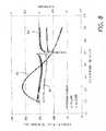
図8を参照すると、リターダンス83、偏光依存損失(PDL)84および挿入損(IL)85が、アルミニウム基板上に配置された、高さ0.97マイクロメートルのTa2O5リッジを0.8マイクロメートルのピッチで有し、リッジ間の溝に屈折率1.0の空気が延在しているサブ波長格子の上記定義の充填率の関数としてプロットされている。リターダンス83は、TM偏光のゼロ次の回折光の位相とTE偏光のゼロ次の回折光の位相の間の差である。充填率約0.46で、半波長のリターダンスが生じていることが分かる。PDLは、約0.08dBであり、平均ILは、約0.2dBである。Referring to FIG. 8, a
図3Bの格子構造は、空気で充填した溝に対応するように修正することができる。格子構造34の上に薄く平らな膜(図示せず)を配置して、格子リッジ34Aの間に空気チャネル34Cを形成し、これらのチャネルを密閉することにより、層36の液晶流体が空気チャネル34Cを充填することを防止し、後に配置される配向層37のための平坦化表面を形成することができる。この目的のために、例えばSiO2膜を使用することができる。The lattice structure of FIG. 3B can be modified to accommodate grooves filled with air. A thin flat membrane (not shown) is placed over the
次に図9を参照し、さらに図3Bを参照すると、ピクセル電極31と透明背面電極32の間に印加されるピクセル電圧の関数として、液晶層36の両端間の電圧降下がプロットされている。直線91(菱形)は、サブ波長格子34の代わりに従来の4分の1波長板(図示せず)を挿入した場合に対応する。直線92(方形)は、図3Bに示す場合、すなわちサブ波長格子34を使用する場合に対応する。サブ波長格子34を使用することにより、同じピクセル電圧で液晶層36の両端間の電圧降下が約2倍になり、可変光学位相差のレベルを大幅に高めることができる。 Referring now to FIG. 9 and further to FIG. 3B, the voltage drop across the
以上の本発明の1つまたは複数の実施形態の記述は、例示および説明を目的として与えたものである。以上の説明は、全てを網羅する、または開示した形態そのものに本発明を限定するためのものではない。上記の教示に照らして、様々な修正および変形が可能である。本発明の範囲は、この詳細な説明によって限定されるのではなく、本明細書に添付する特許請求の範囲によって限定されるものとする。 The foregoing description of one or more embodiments of the invention has been presented for purposes of illustration and description. The above description is not intended to be exhaustive or to limit the invention to the precise form disclosed. Various modifications and variations are possible in light of the above teaching. It is intended that the scope of the invention be limited not by this detailed description, but rather by the claims appended hereto.
20 可変光学リターダ
21 第1の板状電極
22 第2の板状電極
24 サブ波長格子
25 格子線
26 液晶層
27 ディレクタ
28 光ビーム20 variable
Claims (19)
Translated fromJapanese前記ピクセル電極に対向する、実質的に透明な連続的な板状電極と、
前記ピクセル電極と前記実質的に透明な連続的な板状電極の間に電圧が印加されたときに前記実質的に透明な連続的な板状電極に入射する光に可変光学位相差を与える、前記ピクセル電極と前記実質的に透明な連続的な板状電極の間に配置され、ディレクタを有する液晶層と、
前記液晶層と前記ピクセル電極の間に配置され、前記ディレクタに対して鋭角をなす格子線を有するサブ波長格子とを含み、
前記格子線は、リッジを含み、前記リッジ間には隙間があり、
前記リッジは、基板内に形成され、前記ピクセル電極は、前記基板内に位置し、
前記基板、前記リッジ及び前記ピクセル電極は、前記液晶層と前記基板の間に配置される平坦な配向層の前記液晶層とは反対側に位置し、
前記ピクセル電極の凸部は、前記サブ波長格子とは反対の方向に延びている、液晶可変光学リターダ。A pixel electrode;
A substantially transparent continuous plate electrode facing the pixel electrode;
Providing a variable optical phase difference to light incident on the substantially transparent continuous plate electrode when a voltage is applied between the pixel electrode and the substantially transparent continuous plate electrode; A liquid crystal layer disposed between the pixel electrode and the substantially transparent continuous plate electrode and having a director;
A sub-wavelength grating disposed between the liquid crystal layer and the pixel electrode and having a grating line forming an acute angle with respect to the director;
The lattice lines include ridges, and there are gaps between the ridges,
The ridge is formed in a substrate, and the pixel electrode is located in the substrate;
The substrate, the ridge, and the pixel electrode are located on a side opposite to the liquid crystal layer of a flat alignment layer disposed between the liquid crystal layer and the substrate,
Projections of the pixel electrode, the sub-wavelength grating andextending Biteiruin the opposite direction, the liquid crystal variable optical retarder.
基板と、
ピクセル電極と、
入射する光ビームに第1の光学位相差を与える、前記ピクセル電極上に配置されたサブ波長格子であり、互いに平行に延びる複数の格子線を有するサブ波長格子と、
内部を伝搬する光ビームに第2の光学位相差を与える、前記サブ波長格子上に配置された液晶層と、
前記液晶層上に配置された実質的に透明な背面電極とを含み、
前記ピクセル電極と前記実質的に透明な背面電極の間に電圧が印加されたときに前記第2の光学位相差が変化することにより、前記液晶層を通って伝搬する光ビームに可変位相遅延を与え、
前記液晶層のディレクタが、前記複数の格子線に対して鋭角をなすことにより、前記可変光学リターダの前記光ビームの偏光状態に対する感度が低下し、
前記複数の格子線は、リッジを含み、前記リッジ間には隙間があり、
前記リッジは、前記基板内に形成され、前記ピクセル電極は、前記基板内に位置し、
前記基板、前記リッジ及び前記ピクセル電極は、前記液晶層と前記基板の間に配置される平坦な配向層の前記液晶層とは反対側に位置し、
前記ピクセル電極の凸部は、前記サブ波長格子とは反対の方向に延びている、可変光学リターダ。A variable optical retarder that provides a variable phase delay to an incident light beam,
A substrate,
A pixel electrode;
A sub-wavelength grating disposed on the pixel electrode for providing a first optical phase difference to an incident light beam, the sub-wavelength grating having a plurality of grating lines extending in parallel to each other;
A liquid crystal layer disposed on the sub-wavelength grating to give a second optical phase difference to the light beam propagating therein;
A substantially transparent back electrode disposed on the liquid crystal layer,
When the voltage is applied between the pixel electrode and the substantially transparent back electrode, the second optical phase difference changes, thereby causing a variable phase delay in the light beam propagating through the liquid crystal layer. Give,
The director of the liquid crystal layer makes an acute angle with respect to theplurality of lattice lines, thereby reducing the sensitivity of the variable optical retarder to the polarization state of the light beam,
The plurality of grid lines include ridges, and there are gaps between the ridges,
The ridge is formed in the substrate, and the pixel electrode is located in the substrate;
The substrate, the ridge, and the pixel electrode are located on a side opposite to the liquid crystal layer of a flat alignment layer disposed between the liquid crystal layer and the substrate,
Projections of the pixel electrode, the sub-wavelength grating andextending Biteiruin the opposite direction, the variable optical retarder.
前記可変光学リターダが、前記複数のピクセル電極の下で前記シリコン基板上に配置された、前記複数のピクセル電極のそれぞれに独立して電圧を印加するドライバ回路をさらに含む、請求項15に記載の可変光学リターダ。The substrate is a silicon substrate;
The variable optical retarder further includes a driver circuit disposed on the silicon substrate under the plurality of pixel electrodes and independently applying a voltage to each of the plurality of pixel electrodes. Variable optical retarder.
(a)前記光ビームを液晶層を通して伝搬させ、次いで前記液晶層のディレクタに対して鋭角をなすように配向された格子線を有するサブ波長格子を通して伝搬させるステップと、
(b)ステップ(a)で伝搬した光ビームを反射して、前記液晶層を逆に通して伝搬させるステップと、
(c)ステップ(a)および(b)を実行しながら、前記液晶層および前記サブ波長格子の外部にある、前記液晶層および前記サブ波長格子と平行な、平坦な上面を有するピクセル電極と、付加的な平坦な電極とを介して前記液晶層に電界を印加して、前記液晶層の光学位相差を変化させることにより、前記光ビームの位相遅延を変化させるステップとを含み、
前記ピクセル電極および前記付加的な平坦な電極により、前記印加電界の空間的均一性が促進され、それにより前記液晶層の前記変化後の光学位相差の空間的均一性が促進され、
前記格子線は、リッジを含み、前記リッジ間には隙間があり、
前記リッジは、基板内に形成され、前記ピクセル電極は、前記基板内に位置し、
前記基板、前記リッジ及び前記ピクセル電極は、前記液晶層と前記基板の間に配置される平坦な配向層の前記液晶層とは反対側に位置し、 前記ピクセル電極の凸部は、前記サブ波長格子とは反対の方向に延びている、方法。A method of providing a variable phase delay to a light beam,
(A) propagating the light beam through a liquid crystal layer and then propagating through a subwavelength grating having a grating line oriented to form an acute angle with respect to the director of the liquid crystal layer;
(B) reflecting the light beam propagated in step (a) and propagating it through the liquid crystal layer;
(C) a pixel electrode having a flat top surface parallel to the liquid crystal layer and the sub-wavelength grating outside the liquid crystal layer and the sub-wavelength grating while performing steps (a) and (b); Changing the phase delay of the light beam by applying an electric field to the liquid crystal layer via an additional flat electrode to change the optical phase difference of the liquid crystal layer, and
The pixel electrode and the additional flat electrode promote spatial uniformity of the applied electric field, thereby promoting spatial uniformity of the changed optical phase difference of the liquid crystal layer,
The lattice lines include ridges, and there are gaps between the ridges,
The ridge is formed in a substrate, and the pixel electrode is located in the substrate;
The substrate, the ridge, and the pixel electrode are located on a side opposite to the liquid crystal layer of a flat alignment layer disposed between the liquid crystal layer and the substrate, andthe convex portion of the pixel electrode has the sub-wavelengthextending Biteiru methodin the direction opposite to the grating.
The method of claim 18, wherein step (d) comprises forming the subwavelength grating without any metal.
Applications Claiming Priority (2)
| Application Number | Priority Date | Filing Date | Title |
|---|---|---|---|
| US201261692896P | 2012-08-24 | 2012-08-24 | |
| US61/692,896 | 2012-08-24 |
Publications (2)
| Publication Number | Publication Date |
|---|---|
| JP2014044424A JP2014044424A (en) | 2014-03-13 |
| JP6285662B2true JP6285662B2 (en) | 2018-02-28 |
Family
ID=48918306
Family Applications (1)
| Application Number | Title | Priority Date | Filing Date |
|---|---|---|---|
| JP2013170918AActiveJP6285662B2 (en) | 2012-08-24 | 2013-08-21 | Variable optical retarder |
Country Status (4)
| Country | Link |
|---|---|
| US (2) | US9946134B2 (en) |
| EP (1) | EP2700987B1 (en) |
| JP (1) | JP6285662B2 (en) |
| CN (1) | CN103631056B (en) |
Families Citing this family (28)
| Publication number | Priority date | Publication date | Assignee | Title |
|---|---|---|---|---|
| US9726887B2 (en) | 2012-02-15 | 2017-08-08 | Microsoft Technology Licensing, Llc | Imaging structure color conversion |
| US9368546B2 (en) | 2012-02-15 | 2016-06-14 | Microsoft Technology Licensing, Llc | Imaging structure with embedded light sources |
| US9779643B2 (en) | 2012-02-15 | 2017-10-03 | Microsoft Technology Licensing, Llc | Imaging structure emitter configurations |
| US9578318B2 (en) | 2012-03-14 | 2017-02-21 | Microsoft Technology Licensing, Llc | Imaging structure emitter calibration |
| US11068049B2 (en) | 2012-03-23 | 2021-07-20 | Microsoft Technology Licensing, Llc | Light guide display and field of view |
| US9558590B2 (en) | 2012-03-28 | 2017-01-31 | Microsoft Technology Licensing, Llc | Augmented reality light guide display |
| US10191515B2 (en) | 2012-03-28 | 2019-01-29 | Microsoft Technology Licensing, Llc | Mobile device light guide display |
| US9717981B2 (en) | 2012-04-05 | 2017-08-01 | Microsoft Technology Licensing, Llc | Augmented reality and physical games |
| US10502876B2 (en) | 2012-05-22 | 2019-12-10 | Microsoft Technology Licensing, Llc | Waveguide optics focus elements |
| EP2700987B1 (en) | 2012-08-24 | 2017-04-26 | Lumentum Operations LLC | Variable Optical Retarder |
| US10192358B2 (en) | 2012-12-20 | 2019-01-29 | Microsoft Technology Licensing, Llc | Auto-stereoscopic augmented reality display |
| US10592080B2 (en) | 2014-07-31 | 2020-03-17 | Microsoft Technology Licensing, Llc | Assisted presentation of application windows |
| US10678412B2 (en) | 2014-07-31 | 2020-06-09 | Microsoft Technology Licensing, Llc | Dynamic joint dividers for application windows |
| US10254942B2 (en) | 2014-07-31 | 2019-04-09 | Microsoft Technology Licensing, Llc | Adaptive sizing and positioning of application windows |
| US10317677B2 (en) | 2015-02-09 | 2019-06-11 | Microsoft Technology Licensing, Llc | Display system |
| US9827209B2 (en) | 2015-02-09 | 2017-11-28 | Microsoft Technology Licensing, Llc | Display system |
| US11086216B2 (en) | 2015-02-09 | 2021-08-10 | Microsoft Technology Licensing, Llc | Generating electronic components |
| US10018844B2 (en) | 2015-02-09 | 2018-07-10 | Microsoft Technology Licensing, Llc | Wearable image display system |
| CN104765216B (en)* | 2015-04-30 | 2017-12-19 | 京东方科技集团股份有限公司 | Array base palte and preparation method thereof and display device |
| CN108603978B (en)* | 2015-12-09 | 2021-09-21 | 菲尼萨公司 | Polarization independent multiplexer/demultiplexer |
| CN106019456B (en)* | 2016-08-15 | 2018-05-25 | 青岛大学 | A kind of achromatic phase retarder of metal dielectric film grating |
| US10466394B2 (en)* | 2017-01-27 | 2019-11-05 | Magic Leap, Inc. | Diffraction gratings formed by metasurfaces having differently oriented nanobeams |
| CN106707578B (en)* | 2017-03-20 | 2020-02-28 | 京东方科技集团股份有限公司 | Liquid crystal grating, display device and control method thereof |
| WO2019066429A1 (en)* | 2017-09-26 | 2019-04-04 | 주식회사 엘지화학 | Optical film, optical element, and imaging device |
| CN108828717B (en)* | 2018-06-08 | 2019-08-20 | 武汉大学 | Optical path unidirectional conduction element structure based on metasurface blazed grating and its application |
| CN111045230B (en)* | 2019-12-30 | 2023-01-03 | 上海天马微电子有限公司 | Spatial light modulator, manufacturing method thereof and holographic 3D display equipment |
| CN114509838B (en)* | 2022-01-05 | 2023-11-14 | 中国科学院苏州纳米技术与纳米仿生研究所 | Gallium nitride-based laser and preparation method of gallium nitride nano-superstructure in gallium nitride-based laser |
| WO2024256006A1 (en)* | 2023-06-15 | 2024-12-19 | Huawei Technologies Co., Ltd. | Polarization-independent liquid crystal micro-display |
Family Cites Families (30)
| Publication number | Priority date | Publication date | Assignee | Title |
|---|---|---|---|---|
| US4729640A (en)* | 1984-10-03 | 1988-03-08 | Canon Kabushiki Kaisha | Liquid crystal light modulation device |
| US5299289A (en)* | 1991-06-11 | 1994-03-29 | Matsushita Electric Industrial Co., Ltd. | Polymer dispersed liquid crystal panel with diffraction grating |
| JP3568662B2 (en) | 1995-12-08 | 2004-09-22 | 富士通ディスプレイテクノロジーズ株式会社 | LCD panel |
| JPH10104565A (en) | 1996-09-30 | 1998-04-24 | Sony Corp | Reflection type guest-host liquid crystal display device |
| JPH11326899A (en) | 1998-05-19 | 1999-11-26 | Seiko Epson Corp | Reflective liquid crystal device and electronic equipment |
| JP4651791B2 (en)* | 2000-08-29 | 2011-03-16 | Nec液晶テクノロジー株式会社 | Reflective liquid crystal display device, manufacturing method thereof, and driving method thereof |
| WO2003019247A1 (en) | 2001-08-24 | 2003-03-06 | Asahi Glass Company, Limited | Multi-layer diffraction type polarizer and liquid crystal element |
| JP4382317B2 (en) | 2001-12-06 | 2009-12-09 | シチズンホールディングス株式会社 | Liquid crystal variable wavelength filter device |
| EP1629322A1 (en) | 2003-05-22 | 2006-03-01 | Koninklijke Philips Electronics N.V. | Liquid crystal display device having form birefringent compensator |
| US8164721B2 (en) | 2003-12-11 | 2012-04-24 | Tan Kim L | Grating trim retarders |
| US20050232530A1 (en) | 2004-04-01 | 2005-10-20 | Jason Kekas | Electronically controlled volume phase grating devices, systems and fabrication methods |
| EP1780582A4 (en)* | 2004-07-29 | 2009-07-08 | Asahi Glass Co Ltd | POLARIZED DIFFRACTION FILTER AND LAYERED POLYMER DIFFRACTION FILTER |
| US7209212B2 (en)* | 2004-09-15 | 2007-04-24 | China Institute Of Technology | Tunable optical integrated element using liquid crystal as active layer |
| JP2007199241A (en) | 2006-01-25 | 2007-08-09 | Seiko Epson Corp | Liquid crystal device, method for manufacturing liquid crystal device, and projection display device |
| JP4304523B2 (en) | 2006-05-26 | 2009-07-29 | ソニー株式会社 | Reflective liquid crystal projector and image reproducing apparatus |
| JP4747053B2 (en) | 2006-08-15 | 2011-08-10 | Nec液晶テクノロジー株式会社 | Liquid crystal display element and electronic device equipped with the same |
| JP5051830B2 (en) | 2007-05-22 | 2012-10-17 | 株式会社リコー | Polarized illumination device and projection-type image display device |
| US7918600B2 (en) | 2007-08-09 | 2011-04-05 | Panasonic Corporation | Planar illumination device and liquid crystal display device using the same |
| CN101911191B (en)* | 2007-12-27 | 2012-10-24 | 旭硝子株式会社 | Liquid crystal element, optical head device, and variable optical modulation element |
| US20090231702A1 (en)* | 2008-03-17 | 2009-09-17 | Qihong Wu | Optical films and methods of making the same |
| WO2010014624A2 (en)* | 2008-07-28 | 2010-02-04 | Pixel Qi Corporation | Diffractive liquid crystal display |
| JP5077367B2 (en) | 2010-01-28 | 2012-11-21 | 凸版印刷株式会社 | Color filter substrate for transflective liquid crystal display device, manufacturing method thereof, and transflective liquid crystal display device |
| JP5337751B2 (en) | 2010-03-15 | 2013-11-06 | 株式会社ジャパンディスプレイ | Polarizing plate and liquid crystal display device |
| JP2012037396A (en) | 2010-08-06 | 2012-02-23 | Seiko Epson Corp | Optical sensor |
| JP2012074111A (en) | 2010-09-29 | 2012-04-12 | Toppan Printing Co Ltd | Wide band quarter-wave plate |
| JP2012108354A (en) | 2010-11-18 | 2012-06-07 | Toppan Printing Co Ltd | Reflection type phase difference plate |
| US9065707B2 (en) | 2011-09-15 | 2015-06-23 | Finisar Corporation | Polarization-independent LCOS device |
| GB201201190D0 (en) | 2012-01-25 | 2012-03-07 | Cambridge Entpr Ltd | Optical device and methods |
| EP2700987B1 (en) | 2012-08-24 | 2017-04-26 | Lumentum Operations LLC | Variable Optical Retarder |
| WO2015077127A1 (en) | 2013-11-21 | 2015-05-28 | Finisar Corporation | High reflectivity lcos device |
- 2013
- 2013-08-08EPEP13179773.0Apatent/EP2700987B1/enactiveActive
- 2013-08-08USUS13/962,069patent/US9946134B2/enactiveActive
- 2013-08-21JPJP2013170918Apatent/JP6285662B2/enactiveActive
- 2013-08-26CNCN201310377104.XApatent/CN103631056B/enactiveActive
- 2018
- 2018-04-16USUS15/954,132patent/US10747044B2/enactiveActive
Also Published As
| Publication number | Publication date |
|---|---|
| US20140055695A1 (en) | 2014-02-27 |
| US10747044B2 (en) | 2020-08-18 |
| EP2700987B1 (en) | 2017-04-26 |
| CN103631056B (en) | 2018-03-27 |
| EP2700987A1 (en) | 2014-02-26 |
| CN103631056A (en) | 2014-03-12 |
| JP2014044424A (en) | 2014-03-13 |
| US9946134B2 (en) | 2018-04-17 |
| US20180231813A1 (en) | 2018-08-16 |
Similar Documents
| Publication | Publication Date | Title |
|---|---|---|
| JP6285662B2 (en) | Variable optical retarder | |
| US10473839B2 (en) | Reflective LC devices including thin film metal grating | |
| KR102635809B1 (en) | Device for combining light beams which interact with adjacently arranged pixels of a light modulator | |
| CN108351089B (en) | Waveguide coating or substrate for improved intensity distribution | |
| US20200183202A1 (en) | Liquid crystal display panel, liquid crystal display device and display method thereof | |
| CN107466372B (en) | waveguide grating device | |
| JP6457924B2 (en) | Liquid crystal display | |
| US12222499B2 (en) | Eye glow suppression in waveguide based displays | |
| CN106324898B (en) | Display panel and display device | |
| US10353238B2 (en) | Liquid crystal lens and 3D display device | |
| CN102636901B (en) | The method of display panel and manufacture display device | |
| JP2008102416A (en) | Wire grid polarizer and liquid crystal display using the same | |
| JP2005173037A (en) | Liquid crystal display device and manufacturing method thereof | |
| KR20020066406A (en) | Imbedded wire grid polarizer for the visible spectrum | |
| JP2003295153A (en) | Optical deflection apparatus and optical deflection method | |
| KR101098202B1 (en) | Polarized diffractive filter and layered polarized diffractive filter | |
| JP4717087B2 (en) | Optical deflection device | |
| JP2005003758A (en) | Reflective light modulator and variable optical attenuator | |
| US20160246083A1 (en) | Optical modulation device and driving method thereof | |
| CN206096696U (en) | Display panel and display apparatus | |
| US12044921B2 (en) | Spatial light modulator and method of forming the same | |
| KR101832265B1 (en) | Active optical device and display apparatus including the same | |
| Ye et al. | Liquid Crystal on Silicon Application Challenges in WSS | |
| KR20220115620A (en) | Light modulator with high light efficiency | |
| JP2007121642A (en) | Liquid crystal display device |
Legal Events
| Date | Code | Title | Description |
|---|---|---|---|
| RD02 | Notification of acceptance of power of attorney | Free format text:JAPANESE INTERMEDIATE CODE: A7422 Effective date:20160524 | |
| A621 | Written request for application examination | Free format text:JAPANESE INTERMEDIATE CODE: A621 Effective date:20160603 | |
| RD04 | Notification of resignation of power of attorney | Free format text:JAPANESE INTERMEDIATE CODE: A7424 Effective date:20160603 | |
| A711 | Notification of change in applicant | Free format text:JAPANESE INTERMEDIATE CODE: A711 Effective date:20160708 | |
| A977 | Report on retrieval | Free format text:JAPANESE INTERMEDIATE CODE: A971007 Effective date:20170124 | |
| A131 | Notification of reasons for refusal | Free format text:JAPANESE INTERMEDIATE CODE: A131 Effective date:20170221 | |
| A521 | Request for written amendment filed | Free format text:JAPANESE INTERMEDIATE CODE: A523 Effective date:20170515 | |
| A131 | Notification of reasons for refusal | Free format text:JAPANESE INTERMEDIATE CODE: A131 Effective date:20170613 | |
| A521 | Request for written amendment filed | Free format text:JAPANESE INTERMEDIATE CODE: A523 Effective date:20170904 | |
| A02 | Decision of refusal | Free format text:JAPANESE INTERMEDIATE CODE: A02 Effective date:20170919 | |
| A521 | Request for written amendment filed | Free format text:JAPANESE INTERMEDIATE CODE: A523 Effective date:20171205 | |
| A911 | Transfer to examiner for re-examination before appeal (zenchi) | Free format text:JAPANESE INTERMEDIATE CODE: A911 Effective date:20171212 | |
| TRDD | Decision of grant or rejection written | ||
| A01 | Written decision to grant a patent or to grant a registration (utility model) | Free format text:JAPANESE INTERMEDIATE CODE: A01 Effective date:20180123 | |
| A61 | First payment of annual fees (during grant procedure) | Free format text:JAPANESE INTERMEDIATE CODE: A61 Effective date:20180202 | |
| R150 | Certificate of patent or registration of utility model | Ref document number:6285662 Country of ref document:JP Free format text:JAPANESE INTERMEDIATE CODE: R150 | |
| R250 | Receipt of annual fees | Free format text:JAPANESE INTERMEDIATE CODE: R250 | |
| R250 | Receipt of annual fees | Free format text:JAPANESE INTERMEDIATE CODE: R250 | |
| R250 | Receipt of annual fees | Free format text:JAPANESE INTERMEDIATE CODE: R250 | |
| R250 | Receipt of annual fees | Free format text:JAPANESE INTERMEDIATE CODE: R250 | |
| R250 | Receipt of annual fees | Free format text:JAPANESE INTERMEDIATE CODE: R250 |