JP6280697B2 - Power amplifier device and compensation method thereof - Google Patents
Power amplifier device and compensation method thereofDownload PDFInfo
- Publication number
- JP6280697B2 JP6280697B2JP2013110807AJP2013110807AJP6280697B2JP 6280697 B2JP6280697 B2JP 6280697B2JP 2013110807 AJP2013110807 AJP 2013110807AJP 2013110807 AJP2013110807 AJP 2013110807AJP 6280697 B2JP6280697 B2JP 6280697B2
- Authority
- JP
- Japan
- Prior art keywords
- signal
- correction
- circuit
- power amplifier
- frequency
- Prior art date
- Legal status (The legal status is an assumption and is not a legal conclusion. Google has not performed a legal analysis and makes no representation as to the accuracy of the status listed.)
- Active
Links
- 238000000034methodMethods0.000titleclaimsdescription15
- 238000001514detection methodMethods0.000claimsdescription5
- 238000010586diagramMethods0.000description16
- 230000004048modificationEffects0.000description12
- 238000012986modificationMethods0.000description12
- 230000008569processEffects0.000description9
- 230000007423decreaseEffects0.000description6
- 230000005540biological transmissionEffects0.000description5
- 230000010363phase shiftEffects0.000description4
- 239000003990capacitorSubstances0.000description3
- 238000006243chemical reactionMethods0.000description2
- 230000009467reductionEffects0.000description2
- 230000004044responseEffects0.000description2
- 102100035353Cyclin-dependent kinase 2-associated protein 1Human genes0.000description1
- 101000760620Homo sapiens Cell adhesion molecule 1Proteins0.000description1
- 101000737813Homo sapiens Cyclin-dependent kinase 2-associated protein 1Proteins0.000description1
- 101000710013Homo sapiens Reversion-inducing cysteine-rich protein with Kazal motifsProteins0.000description1
- 101000661807Homo sapiens Suppressor of tumorigenicity 14 proteinProteins0.000description1
- 101000585359Homo sapiens Suppressor of tumorigenicity 20 proteinProteins0.000description1
- 101100033865Saccharomyces cerevisiae (strain ATCC 204508 / S288c) RFA1 geneProteins0.000description1
- 101100524516Saccharomyces cerevisiae (strain ATCC 204508 / S288c) RFA2 geneProteins0.000description1
- 102100029860Suppressor of tumorigenicity 20 proteinHuman genes0.000description1
- 230000008859changeEffects0.000description1
- 230000001419dependent effectEffects0.000description1
- 238000007599dischargingMethods0.000description1
- 230000010355oscillationEffects0.000description1
Images


Landscapes
- Amplifiers (AREA)
Description
Translated fromJapanese本発明は,パワーアンプ装置及びその補償方法に関する。 The present invention relates to a power amplifier device and a compensation method thereof.
パワーアンプは,無線送信機などに設けられ,例えば,ベースバンド信号をキャリア信号で直交変調した信号を高電力増幅する回路である。 The power amplifier is a circuit that is provided in a wireless transmitter or the like and amplifies a signal obtained by orthogonally modulating a baseband signal with a carrier signal, for example, with high power.
パワーアンプの電力効率は出力信号レベルを消費電力で除算した値であり,一般に,より高いレベルの入力信号を増幅する場合に高い電力効率になる。 The power efficiency of the power amplifier is a value obtained by dividing the output signal level by the power consumption. In general, the power efficiency becomes high when a higher level input signal is amplified.
一方で,パワーアンプは,低レベルの入力信号は線型増幅することができるが,高レベルの入力信号はその飽和特性により非線型増幅になる。したがって,パワーアンプを高い電力効率で動作させると,増幅した出力信号に非線型歪みが発生する。そこで,増幅した出力信号の非線型歪みを検出し,非線形歪みの逆特性で入力側の信号を補正してパワーアンプに入力することで,パワーアンプの入出力特性を線型化することが提案されている。このようなプリディストーション式の非線型歪み補償回路について,例えば,以下の特許文献等に記載されている。 On the other hand, a power amplifier can linearly amplify a low level input signal, but a high level input signal is nonlinearly amplified due to its saturation characteristic. Therefore, when the power amplifier is operated with high power efficiency, nonlinear distortion occurs in the amplified output signal. Therefore, it has been proposed to linearize the input / output characteristics of the power amplifier by detecting the nonlinear distortion of the amplified output signal, correcting the input signal with the inverse characteristic of the nonlinear distortion and inputting it to the power amplifier. ing. Such a predistortion type non-linear distortion compensation circuit is described in, for example, the following patent documents.
パワーアンプの非線形歪みは入力信号の周波数に依存して異なるため,入力信号の周波数帯域が広くなると,信号帯域の中心周波数で非線形歪み補償を行っても信号帯域全体で適切に非線形歪みを補償することは困難である。 Since the nonlinear distortion of the power amplifier varies depending on the frequency of the input signal, if the frequency band of the input signal becomes wide, even if nonlinear distortion compensation is performed at the center frequency of the signal band, the nonlinear distortion is compensated appropriately over the entire signal band It is difficult.
そのため,先行文献1などでは,異なる周波数帯域の非線形歪みを複数の直交復調部により検出し,入力側のベースバンド信号に非線形歪みの逆極性のベースバンド信号を重畳している。 For this reason, in the
しかしながら,上記の方法では,複数の直交復調部により異なる周波数帯域の非線形歪み補正値を生成しているので,その複数の直交復調部のばらつきによりそれぞれの非線形歪み成分やそれに基づく補正値にばらつきが生じて,適切に非線形歪み補償を行うことが困難になる。また,複数の直交復調部を設けることは回路規模の増大を招く。 However, in the above method, the nonlinear distortion correction values in different frequency bands are generated by the plurality of orthogonal demodulation units, and therefore variations in the nonlinear distortion components and the correction values based on the nonlinear distortion components due to variations in the plurality of orthogonal demodulation units. As a result, it becomes difficult to perform nonlinear distortion compensation appropriately. In addition, providing a plurality of orthogonal demodulation units causes an increase in circuit scale.
そこで,本発明の目的は,回路規模が小さく,信号帯域全体で適切に非線形歪みを補償するパワーアンプ装置及びその補償方法を提供することにある。 SUMMARY OF THE INVENTION An object of the present invention is to provide a power amplifier device that has a small circuit scale and appropriately compensates for nonlinear distortion over the entire signal band, and a compensation method thereof.
実施の形態のパワーアンプ装置の第1の側面は,第1のベースバンド信号をキャリア信号により直交変調する直交変調回路と,
前記直交変調回路が生成する第1の信号を電力増幅する電力増幅器と,
前記電力増幅器の出力からフィードバックされた第2の信号を前記キャリア信号により直交復調して第2のベースバンド信号を生成する直交復調回路と,
前記第1のベースバンド信号と第2のベースバンド信号との差分に基づいて前記電力増幅器の出力信号の非線形歪みを検出し,前記検出結果に基づいて前記第1のベースバンド信号を補正する歪み補正回路とを有し,
前記歪み補正回路は,前記直交変調回路と直交復調回路を第1の周波数のキャリア信号で変調及び復調させた時に検出する第1の非線形歪みに基づいて第1の補正値を求め,前記直交変調回路と直交復調回路を前記第1の周波数と異なる第2の周波数のキャリア信号で変調及び復調させた時に検出する第2の非線形歪みに基づいて第2の補正値を求め,前記第1及び第2の補正値で前記第1のベースバンド信号を補正する。A first aspect of the power amplifier device according to the embodiment includes an orthogonal modulation circuit that orthogonally modulates the first baseband signal with a carrier signal;
A power amplifier that amplifies the first signal generated by the quadrature modulation circuit;
A quadrature demodulation circuit for quadrature demodulating the second signal fed back from the output of the power amplifier with the carrier signal to generate a second baseband signal;
Distortion for detecting nonlinear distortion of the output signal of the power amplifier based on the difference between the first baseband signal and the second baseband signal and correcting the first baseband signal based on the detection result A correction circuit,
The distortion correction circuit obtains a first correction value based on a first nonlinear distortion detected when the quadrature modulation circuit and the quadrature demodulation circuit are modulated and demodulated with a carrier signal having a first frequency, and the quadrature modulation A second correction value is obtained based on a second nonlinear distortion detected when the circuit and the orthogonal demodulation circuit are modulated and demodulated with a carrier signal having a second frequency different from the first frequency, and the first and second correction values are obtained. The first baseband signal is corrected with a correction value of 2.
第1の側面によれば,単一の直交復調回路を利用しているので,回路規模が小さく,周波数が異なる第1,第2の周波数のキャリア信号で復調した時に検出した第1,第2の非線形歪みに基づいて第1,第2の補正値を求め,その第1,第2の補正値で第1のベースバンド信号を補正するので,信号帯域全体にわたり適切に非線形歪み補償を行うことができ,しかも,回路規模が小さい。 According to the first aspect, since a single quadrature demodulation circuit is used, the first and second detected when demodulating with carrier signals of the first and second frequencies having a small circuit scale and different frequencies. Since the first and second correction values are obtained based on the non-linear distortion and the first baseband signal is corrected with the first and second correction values, the non-linear distortion compensation is appropriately performed over the entire signal band. In addition, the circuit scale is small.
[実施の形態におけるパワーアンプ装置]
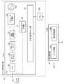
図1は,本実施の形態におけるパワーアンプ装置の構成図である。パワーアンプ装置は,送信側回路1と受信側回路2と,アンテナATと,アンテナATを送信側回路1と受信側回路2に切り替えるデュプレクサ12とを有する。[Power Amplifier Device in Embodiment]
FIG. 1 is a configuration diagram of a power amplifier device according to the present embodiment. The power amplifier device includes a
パワーアンプ装置は,送信側回路1として,デジタル送信信号S1をアナログのベースバンドのI信号I1,Q信号Q1に変換するDA変換回路13と,キャリア信号SCを生成するキャリア信号生成器11と,キャリア信号SCによりI信号I3とQ信号Q3を直交変調する直交変調回路10と,直交変調された信号S2を電力増幅する電力増幅器PAとを有する。電力増幅器PAの出力信号S3がデュプレクサ12を介してアンテナATから送出される。 The power amplifier device includes, as a
直交変調回路10は,図示しないが,I信号I3にキャリア信号SCを乗算する第1の乗算器と,Q信号Q3にキャリア信号SCの位相をπ/2シフトした信号を乗算する第2の乗算器と,第1,第2の乗算器の出力信号を加算する加算器とを有する。 Although not shown, the quadrature modulation circuit 10 includes a first multiplier that multiplies the I signal I3 by the carrier signal SC, and a second multiplier that multiplies the Q signal Q3 by a signal obtained by shifting the phase of the carrier signal SC by π / 2. And an adder for adding the output signals of the first and second multipliers.
一方,パワーアンプ装置は,受信側回路2として,アンテナATで受信した受信信号S4を増幅するローノイズアンプLNAと,その出力信号S6をスイッチSW1を介して入力しその出力信号S6をキャリア信号SCにより直交復調してベースバンドのI信号I11とQ信号Q11を出力する直交復調回路20と,そのベースバンドのI信号I11とQ信号Q11とを波形成形するバッファ回路BUF3,BUF4と,アナログのI信号Q13とQ信号Q13をデジタルの受信信号S7に変換するAD変換回路21とを有する。 On the other hand, in the power amplifier device, as the
直交復調回路20は,図示しないが,受信信号S6にキャリア信号SCを乗算してI信号I11を生成する第3の乗算器と,受信信号にキャリア信号SCの位相をπ/2シフトした信号を乗算する第4の乗算器とを有する。 Although not shown, the
そして,パワーアンプ装置は,電力増幅器PAの非線形歪みを補償する歪み補正回路を,以下のとおり有する。すなわち,歪み補正回路は,フィードバック経路15と,歪み補正部22と補正制御部24と,初段補正回路100と,終段補正回路200とを有する。 The power amplifier device includes a distortion correction circuit that compensates for nonlinear distortion of the power amplifier PA as follows. That is, the distortion correction circuit includes a
フィードバック経路15には,電力増幅器PAの出力信号S3が分配器14により分岐される。そして,スイッチSW1を介してフィードバックされる信号S6が直交復調回路20に入力される。さらに,歪み補正部22は,直交復調回路20で復調したベースバンドのI信号I11及びQ信号Q11と,直交変調回路10に入力されるベースバンドのI信号I3及びQ信号Q3のI信号,Q信号それぞれの差分に基づいて非線形歪み成分を検出し,非線形歪み成分が低減するような補正値C11-C22でベースバンドのI信号I1,I2とQ信号Q1,Q2を補正する。また,補正制御部24は,非線形歪み成分を検出して補正値を求めるために,歪み補正部22とキャリア信号生成器11とを制御する。 In the
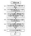
図2は,本実施の形態における非線形歪み補償の動作を示すフローチャート図である。このフローチャート図の処理は,補正制御部24と歪み補正部22の補償動作を示している。 FIG. 2 is a flowchart showing the operation of nonlinear distortion compensation in the present embodiment. The processing in the flowchart shows the compensation operation of the
まず,補正制御部24は,スイッチ制御信号C241によりスイッチSW1をフィードバック経路15側に閉じて,分配器14から分岐された電力増幅器PAの出力信号S3を直交復調回路20に入力させる(ST1)。そして,補正制御部24は,周波数シフト信号C242によりキャリア信号生成器11に第1のキャリア信号SCを生成させる(ST2)。第1のキャリア信号SCは,電力増幅器PAの入出力信号S2,S3の信号帯域の中心周波数fcにオフセット周波数Δfoを減算した第1の周波数fc-Δfoの信号である。 First, the
このように第1のキャリア信号SC(fc-Δfo)が直交変調回路10と直交復調回路20とに入力されることで,歪み補正部22は,直交変調回路10に入力されるベースバンドのI信号I3とQ信号Q3と,直交復調回路20から出力されるベースバンドのI信号I11とQ信号Q11のI信号及びQ信号それぞれの差分に基づいて,第1の周波数fc-Δfoのキャリア信号SCで電力増幅器PAに生成される非線型歪み成分を検出し,その非線形歪み成分を低減する第1の補正値C11,C12を生成し,初段補正回路100で,その第1の補正値C11,C12によりベースバンドのI信号I1とQ信号Q1を補正する(ST3)。具体的には,非線形歪み成分の逆特性でベースバンドのI信号I1とQ信号Q1を補正する。これにより,第1の周波数fc-Δfoでの非線形歪み成分が低減される。 In this way, the first carrier signal SC (fc−Δfo) is input to the quadrature modulation circuit 10 and the
後述するとおり,歪み補正部22は,直交変調回路10に入力されるベースバンドのI信号I3とQ信号Q3と,直交復調回路20から出力されるベースバンドのI信号I11とQ信号Q11との差分に基づく非線形歪み成分を検出する差分検出器と,非線形歪み成分を低減する補正値を生成する補正信号生成器とを有する。 As will be described later, the
次に,補正制御部24は,周波数シフト信号C242によりキャリア信号生成器11に第2のキャリア信号SCを生成させる(ST4)。第2のキャリア信号SCは,電力増幅器PAの入出力信号S2,S3の信号帯域の中心周波数fcにオフセット周波数Δfoを加算した第2の周波数fc+Δfoの信号である。 Next, the
このように第2のキャリア信号SC(fc+Δfo)が直交変調回路10と直交復調回路20とに入力されることで,歪み補正部22は,直交変調回路10に入力されるベースバンドのI信号I3とQ信号Q3と,直交復調回路20から出力されるベースバンドのI信号I11とQ信号Q11のI信号,Q信号それぞれ差分に基づいて,第2の周波数fc+Δfoのキャリア信号SCで電力増幅器PAに生成される非線型歪み成分を検出し,その非線形歪み成分を低減する第2の補正値C21,C22を生成し,終段補正回路200で,その第2の補正値C21,C22によりベースバンドのI信号I2とQ信号Q2を補正する(ST5)。これにより,第2の周波数fc+Δfoでの非線形歪み成分が低減される。 In this way, the second carrier signal SC (fc + Δfo) is input to the quadrature modulation circuit 10 and the
最後に,補正制御部24は,スイッチ制御信号C241によりスイッチSW1をローノイズアンプLNA側に閉じる(ST6)。これで非線形歪み補償の動作を終了する。その後の通常動作では,上記の補正値がそれぞれの補正回路に設定されるので,電力増幅器PAから非線形歪みは低減されている。 Finally, the
上記の実施の形態のパワーアンプ装置の非線形歪み補償回路によれば,共通の直交復調回路20を利用して,第1の周波数fc-Δfoでの非線形歪み成分を検出してそれを低減する第1の補正値でベースバンドのI信号I1とQ信号Q1を補正する動作と,第2の周波数fc+Δfoでの非線形歪み成分を検出してそれを低減する第2の補正値でベースバンドのI信号I2とQ信号Q2を補正する動作とを,時分割で行う。したがって,第1,第2の周波数での非線形歪み成分にずれはなく,適切に2つの周波数領域の非線形歪み成分を低減することができる。また,単一の直交復調回路20を利用するので,回路規模を小さく抑えることができる。さらに,直交復調回路20は,受信回路部2に元々備えられている直交復調回路を利用すれば,更に,回路規模を小さく抑えることができる。 According to the nonlinear distortion compensation circuit of the power amplifier device of the above embodiment, the common
図3,図4,図5は,本実施の形態におけるパワーアンプ装置の非線形歪み補償を説明する図である。図3は,非線形歪み成分に周波数依存性がない理想的な電力増幅器PAについて,(A)周波数fに対する出力レベル(またはゲイン)特性と,(B)周波数fに対する信号帯域BW内の出力信号S3と信号帯域BWの外側の不要波S3Aと補正後の不要波S3Bのレベルを示している。 3, 4, and 5 are diagrams for explaining nonlinear distortion compensation of the power amplifier device according to the present embodiment. FIG. 3 shows (A) an output level (or gain) characteristic with respect to the frequency f and (B) an output signal S3 within the signal band BW with respect to the frequency f, for an ideal power amplifier PA in which the nonlinear distortion component has no frequency dependence. The levels of the unnecessary wave S3A outside the signal band BW and the unnecessary wave S3B after correction are shown.
電力増幅器PAは,前述したとおり,高い電力効率で動作させると出力信号S3の出力レベルが高くなり,ゲインが非線型領域での動作になる。そのため,出力信号S3には非線型歪み成分が含まれる。ただし,図3の理想的な場合は非線形歪み成分に周波数fに対する依存性がないので,図3(A)に示されるとおり,非線形歪み成分を含む出力信号S3の出力レベルは,周波数に対してフラットな特性になっている。このことは,電力増幅器PAの周波数fに対するゲインも一定であることを意味する。そして,図3(B)に示されるように,出力信号S3は信号帯域BW内でその出力レベルはフラットである。 As described above, when the power amplifier PA is operated with high power efficiency, the output level of the output signal S3 increases, and the gain operates in a non-linear region. For this reason, the output signal S3 includes a nonlinear distortion component. However, in the ideal case of FIG. 3, since the nonlinear distortion component does not depend on the frequency f, as shown in FIG. 3A, the output level of the output signal S3 including the nonlinear distortion component is It has a flat characteristic. This means that the gain of the power amplifier PA with respect to the frequency f is also constant. As shown in FIG. 3B, the output level of the output signal S3 is flat within the signal band BW.
なお,図3(A)(B)の出力信号S3の出力レベルには,非線形歪み成分は示されていない。ただし,図3の紙面に垂直な入力信号レベルの軸を想定すると,その垂直な軸に沿って非線型歪み成分が入力信号レベルが高い領域で大きくなる。 Note that the nonlinear distortion component is not shown in the output level of the output signal S3 in FIGS. However, assuming an input signal level axis perpendicular to the paper surface of FIG. 3, the nonlinear distortion component increases along the vertical axis in a region where the input signal level is high.
一方,図3(B)に示されるように,電力増幅器PAの出力信号S3に非線形歪み成分が含まれていると,信号帯域BWの外側の周波数帯域に不要波成分S3Aが生成される。但し,この不要波成分S3Aは,出力信号S3と同様に周波数依存性がない。そして,電力増幅器PAの非線形歪みが信号帯域BWの中心周波数fcで補正されると,出力信号S3に含まれている非線型歪み成分が低減される(図3(B)には低減は示されていない)と共に,その不要波成分S3AもS3Bのように低減される。図示されるとおり,不要波成分S3Aは信号帯域の両側で同等のレベルであり,上記の非線形歪み成分を低減する補正により,不要波成分はS3Bのように信号帯域の両側で同等に低減される。 On the other hand, as shown in FIG. 3B, when a nonlinear distortion component is included in the output signal S3 of the power amplifier PA, an unnecessary wave component S3A is generated in the frequency band outside the signal band BW. However, this unnecessary wave component S3A has no frequency dependence like the output signal S3. When the nonlinear distortion of the power amplifier PA is corrected with the center frequency fc of the signal band BW, the nonlinear distortion component included in the output signal S3 is reduced (the reduction is shown in FIG. 3B). In addition, the unwanted wave component S3A is also reduced as in S3B. As shown in the figure, the unnecessary wave component S3A is at the same level on both sides of the signal band, and the unnecessary wave component is equally reduced on both sides of the signal band as in S3B by the above-described correction for reducing the nonlinear distortion component. .
次に,図4は,非線形歪み成分に周波数依存性がある電力増幅器PAについて,(A)周波数fに対する出力レベル(またはゲイン)特性と,(B)周波数fに対する出力信号S3と不要波S3Aと中心周波数fcでの補正後の不要波S3Bのレベルを示している。この例では,図4(A)に示されるように,電力増幅器PAは,周波数fがより高くなると出力レベル(またはゲイン)が低下している。それに伴い,図4(B)の出力信号S3も,信号帯域BW内で高周波側の出力レベルが低下している。これは図4(A)の電力増幅器PAの非線形歪み成分に周波数依存性があるからである。また,出力信号S3に非線形歪みが生じた結果,不要波S3Aは信号帯域の両側でレベルが異なっている。これは,非線形歪みに周波数依存性があるからである。 Next, FIG. 4 shows (A) an output level (or gain) characteristic with respect to the frequency f, and (B) an output signal S3 and an unnecessary wave S3A with respect to the frequency f. The level of the unwanted wave S3B after correction at the center frequency fc is shown. In this example, as shown in FIG. 4A, the output level (or gain) of the power amplifier PA decreases as the frequency f increases. Accordingly, the output level of the output signal S3 in FIG. 4B also decreases on the high frequency side within the signal band BW. This is because the nonlinear distortion component of the power amplifier PA in FIG. Further, as a result of nonlinear distortion occurring in the output signal S3, the level of the unwanted wave S3A is different on both sides of the signal band. This is because nonlinear distortion has frequency dependency.
そして,図4(B)に示されるように,電力増幅器PAの非線形歪みが信号帯域BWの中心周波数fcで補償されると,出力信号S3に含まれている非線型歪み成分が低減されると共に(この低減は図示されていない),その不要波成分S3AもS3Bのように低減される。ただし,周波数依存性があるので,信号帯域BWの中心周波数fcで歪み補正がされると,信号帯域BWより低周波数側と高周波数側の不要波成分S3Aは,同等レベルまで十分に低減されていない。 As shown in FIG. 4B, when the nonlinear distortion of the power amplifier PA is compensated by the center frequency fc of the signal band BW, the nonlinear distortion component included in the output signal S3 is reduced. (This reduction is not shown), the unnecessary wave component S3A is also reduced like S3B. However, due to frequency dependence, if distortion correction is performed at the center frequency fc of the signal band BW, the unwanted wave component S3A on the low frequency side and high frequency side of the signal band BW is sufficiently reduced to the same level. Absent.
そして,図5は,非線形歪み成分に周波数依存性がある電力増幅器PAについて,(A)周波数fに対する出力レベル(またはゲイン)特性と,(B)周波数fに対する出力信号S3と不要波S3Aと2つの周波数fc-Δfoとfc+Δfoでの補正後の不要波S3Bのレベルを示している。図5には,本実施の形態の歪み補正を適用した場合の補償後の不要波S3Bのレベルが示されている。この例でも,図4(A)と同様に,図5(A)に示されるとおり,電力増幅器PAは,周波数fがより高くなると出力レベル(またはゲイン)が低下している。それに伴い,図5(B)の出力信号S3も,信号帯域BW内で高周波側の出力レベルが低下している。そして,非線形歪み成分に起因する不要波S3Aも,図4(B)と同様に信号帯域BWより高周波側で出力レベルが低下している。 5 shows (A) an output level (or gain) characteristic with respect to the frequency f and (B) an output signal S3 with respect to the frequency f and unnecessary waves S3A and 2 for the power amplifier PA having a frequency dependency in the nonlinear distortion component. The level of the unnecessary wave S3B after correction at two frequencies fc-Δfo and fc + Δfo is shown. FIG. 5 shows the level of the unnecessary wave S3B after compensation when the distortion correction of the present embodiment is applied. In this example as well, as in FIG. 4A, as shown in FIG. 5A, the output level (or gain) of the power amplifier PA decreases as the frequency f increases. Accordingly, the output level of the output signal S3 in FIG. 5B also decreases on the high frequency side within the signal band BW. The output level of the unnecessary wave S3A caused by the nonlinear distortion component is also lowered on the higher frequency side than the signal band BW, as in FIG.
そして,図1,図2で説明したとおり,本実施の形態における非線形歪み成分を2つの周波数fc-Δfoとfc+Δfoで検出し,それぞれの非線形歪み成分が低減されるように補正値で補正した結果,図5(B)に示されるとおり,補正後の不要波成分S3Cは,信号帯域BWの両側の周波数領域で同等レベルまで低減されている。これは,非線形歪み成分が周波数依存性を有することにより,不要波成分S3Cも周波数依存性を有していて,2つの周波数fc-Δfoとfc+Δfoで検出した非線形歪み成分を低減する補正を行ったからである。 As described with reference to FIGS. 1 and 2, the nonlinear distortion component in the present embodiment is detected with two frequencies fc−Δfo and fc + Δfo, and corrected with correction values so that each nonlinear distortion component is reduced. As a result, as shown in FIG. 5B, the unnecessary wave component S3C after correction is reduced to the same level in the frequency domain on both sides of the signal band BW. This is because the non-linear distortion component has frequency dependency, and the unnecessary wave component S3C also has frequency dependency, and correction is performed to reduce the non-linear distortion component detected by the two frequencies fc-Δfo and fc + Δfo. It is because it went.
図6は,本実施の形態における非線形歪み成分を低減する補正に対する初段補正回路と終段補正回路の出力特性と,電力増幅器PAの出力特性とを示す図である。図6(A)(B)(C)において,横軸が周波数,縦軸が出力レベルに対応している。 FIG. 6 is a diagram showing the output characteristics of the first-stage correction circuit and the final-stage correction circuit and the output characteristics of the power amplifier PA for correction for reducing the nonlinear distortion component in the present embodiment. 6A, 6B, and 6C, the horizontal axis corresponds to the frequency, and the vertical axis corresponds to the output level.
図6(A)に示されるように,非線形歪み成分の補正をする前は,初段補正回路100も終段補正回路200もその出力特性は,周波数依存性がないフラットな特性である。一方,電力増幅器PAの出力特性は,周波数に依存する非線形歪み成分が反映され,低周波領域でより高いレベルになり,高周波領域でより低いレベルになっている。 As shown in FIG. 6A, before the nonlinear distortion component is corrected, the output characteristics of the first-
そこで,図6(B)の初段補正回路の補正後の例では,初段補正回路100の出力特性が第1の周波数fc-Δfoでの非線形歪み成分の逆特性で補正される。一方,終段補正回路200には未だ補正されていないので,周波数依存性がないフラットな特性のままである。その結果,電力増幅器PAの出力レベルは,中心周波数fcより低周波領域でフラットになっている。つまり,初段補正回路100において第1の周波数fc-Δfoでの非線形歪み成分を低減する補正が行われたので,電力増幅器PAの出力レベルは低周波領域での非線形歪み成分による特性((A)に示したレベルが上昇する特性)が低減されている。なお,初段補正回路100での補正により,終段補正回路200の出力信号レベルは,図6(B)に破線で示したように低下する。ただし,終段補正回路の特性は実線のようにフラットである。 Therefore, in the example after the correction by the first stage correction circuit of FIG. 6B, the output characteristic of the first
そして,図6(C)の終段補正回路の補正後の例では,終段補正回路200の出力特性が第2の周波数fc+Δfoでの非線形歪み成分の逆特性で補正される。その結果,電力増幅器PAの出力レベルは,中心周波数fcより高周波領域でもフラットになっている。つまり,終段補正回路200において第2の周波数fc+Δfoでの非線形歪み成分を低減する補正が行われたので,電力増幅器PAの出力レベルは高周波領域でも非線形歪み成分による特性((A)に示したレベルが低下する特性)が低減されている。 6C, the output characteristic of the final
なお,第1の周波数fc-Δfoと第2の周波数fc+Δfoの中心周波数fcからのシフト量Δfoは,電力増幅器PAの信号帯域BWに対して,Δfo<BW/2であることが望ましい,これにより,信号帯域BW内の全周波数での非線形歪み成分を適切に低減するよう補正することができる。特に,中心周波数fcでの非線形歪み成分が適切に低減される。 The shift amount Δfo from the center frequency fc of the first frequency fc−Δfo and the second frequency fc + Δfo is preferably Δfo <BW / 2 with respect to the signal band BW of the power amplifier PA. Thereby, it is possible to correct the nonlinear distortion components at all frequencies in the signal band BW so as to be appropriately reduced. In particular, the nonlinear distortion component at the center frequency fc is appropriately reduced.
[本実施の形態のパワーアンプ装置の具体的構成]
図7は,本実施の形態におけるパワーアンプ装置の具体的な構成図である。図7には,図1のパワーアンプ装置と同じ構成が示されているが,図1の初段補正回路100と終段補正回路200と歪み補正部22と補正制御部24とキャリア信号生成器11の構成が更に示されている。[Specific Configuration of Power Amplifier Device of the Present Embodiment]
FIG. 7 is a specific configuration diagram of the power amplifier device according to the present embodiment. 7 shows the same configuration as that of the power amplifier apparatus of FIG. 1, but the first
歪み補正部22は,送信側回路1の直交変調回路10に入力するI信号I3とQ信号Q3(第1のベースバンド信号)と,受信側回路2の直交復調回路20が出力するI信号I11とQ信号Q11(第2のベースバンド信号)とを,スイッチ群SW2を介して入力する差分検出器22Aと,差分検出器22Aが検出した差分に基づく非線形歪み成分22Cに対応する補正値を生成し,その補正値を補正信号C11,C12,C21,C22として出力する補正信号生成器22Bとを有する。この補正信号C11-C22は,スイッチ群SW3を介して,初段補正回路100と終段補正回路200とに供給される。 The
図8は,歪み補正部22内の差分検出器22Aの具体的な構成図である。差分検出器22Aは,正極と負極の入力と正極と負極の出力とを有する差動アンプAMPと,入力端子に接続される1対の入力キャパシタCp,Cnと,差動アンプAMPをリセットするスイッチSW4,SW5と,差動アンプAMPの差動出力の大きさをアナログデジタル変換するADCとを有する。ADCはNビットの差分値を非線形歪み成分22Cとして出力する。 FIG. 8 is a specific configuration diagram of the
差分検出器22Aの入力側には,I信号I3とQ信号Q3(第1のベースバンド信号)とI信号I11とQ信号Q11(第2のベースバンド信号)のうち,2つのI信号I3,I11を選択するか,または,2つのQ信号Q3,Q11を選択するスイッチ群SW2が設けられている。スイッチ群SW2は,補正制御部24が出力するスイッチ制御信号C241により,スイッチSW21,SW23が導通制御されて2つのI信号I3,I11を選択し,スイッチSW22,SW24が導通制御されて2つのQ信号Q3,Q11を選択する。 Of the I signal I3, the Q signal Q3 (first baseband signal), the I signal I11, and the Q signal Q11 (second baseband signal), two I signals I3, A switch group SW2 for selecting I11 or selecting two Q signals Q3 and Q11 is provided. In the switch group SW2, the switches SW21 and SW23 are subjected to conduction control by the switch control signal C241 output from the
差動アンプAMPでは,第1のベースバンド信号(I3,Q3)と第2のベースバンド信号(I11,Q11)の差分を増幅する場合は,スイッチSW4,SW5がオフにされる。そして,スイッチSW21,SW23がオンにされると,差動アンプAMPは,第1,第2のベースバンド信号のI信号I3,I11の差分を増幅する。また,スイッチSW22,SW24がオンにされると,差動アンプAMPは,第1,第2のベースバンド信号のQ信号Q3,Q11の差分を増幅する。その増幅された差分値がADCにより非線形歪み成分22Cとしてそれぞれ出力される。上記のスイッチの制御は,補正制御部24が生成するスイッチ制御信号C241により行われる。 In the differential amplifier AMP, when the difference between the first baseband signal (I3, Q3) and the second baseband signal (I11, Q11) is amplified, the switches SW4, SW5 are turned off. When the switches SW21 and SW23 are turned on, the differential amplifier AMP amplifies the difference between the I signals I3 and I11 of the first and second baseband signals. When the switches SW22 and SW24 are turned on, the differential amplifier AMP amplifies the difference between the Q signals Q3 and Q11 of the first and second baseband signals. The amplified difference values are respectively output as
図7のキャリア信号生成器11は,キャリア信号SCを生成するPLL回路11Aと,キャリア信号SCの周波数を信号帯域の中心周波数からオフセット周波数Δfoだけ低い方向と高い方向にずらす制御を行う周波数シフト部11Bとを有する。また,補正制御部24は,補正制御の開始を指示する補正信号CRに応答して動作するスイッチ制御部24Aと周波数制御部24Bとを有する。この補正信号CRは,例えば,電源起動時や,外部温度が大きく変動した時などに与えられる。そのような場合に,電力増幅器PAの非線形歪み成分を低減する補正動作が実行される。 The
図9は,キャリア信号生成器と補正制御部の具体的な構成図である。キャリア信号生成器11は,PLL回路11Aと周波数シフト部11Bとを有する。PLL回路11Aは,キャリア信号SCを出力し,発振器OSCと,その発振信号を分周してレファレンス信号frを生成するレファレンス分周器31と,出力するキャリア信号SCを分周してバリアブル信号fvを出力するプログラマブル分周器36と,バリアブル信号fvとレファレンス信号frとの位相を比較し位相のずれ方向とずれ量を出力する位相比較器32と,位相比較器32が出力する位相のずれ方向とずれ量を電流に変換する(位相のずれ方向は充電か放電電流に,ずれ量は電荷量に変換)チャージポンプ33と,チャージポンプ33が生成する電流を充電または放電するキャパシタを有するループフィルタ34と,ループフィルタ34のキャパシタ電圧を制御電圧として入力し,その制御電圧に応じた周波数のキャリア信号SCを生成する電圧制御発振器35とを有する。 FIG. 9 is a specific configuration diagram of the carrier signal generator and the correction control unit. The
さらに,PLL回路11Aは,分周比設定ロジック部37を有し,分周比設定ロジック部37は,補正制御部24の周波数制御部24Bが出力する周波数制御信号C242に応じて,プログラマブル分周器36の分周比を設定する。通常,分周比設定ロジック部37は,電力増幅器PAの入力信号の信号帯域の中心周波数fcになるよう分周比を設定する。そして,非線形歪み成分を補正する時に,補正信号CRに応答して補正制御部24の周波数制御部24Bが出力する周波数制御信号C242に応じて,補正周波数シフト部11Bは,中心周波数fcからオフセット量Δfoだけシフトした第1の周波数fc-Δfoまたは第2の周波数fc+Δfoになるように,分周比設定ロジック部37によりプログラマブル分周器36の分周比を設定する。 Further, the
図7の初段補正回路100は,I信号線とQ信号線との間に設けた可変抵抗器101と,I信号線とQ信号線のレベルを補正する補正レベルを生成するデジタルアナログ変換器102と,バッファ回路BUF1とを有する。可変抵抗器101は,補正信号生成器22Bが生成するデジタルの振幅補正信号C11に基づいてその抵抗値が可変制御される。一方,デジタルアナログ変換器102は,補正信号生成器22Bが生成するデジタルの位相補正信号C12に基づいてI信号I1とQ信号Q1のレベルを補正するアナログの補正信号(電圧)を,I信号線とQ信号線とに出力する。補正信号生成器22Bは,差分検出器22Aが検出した第1のベースバンド信号(I3,Q3)と第2のベースバンド信号(I11,Q11)の差分である非線形歪み成分22Cが低減されるように補正信号C11,C12を生成して,I信号I1とQ信号Q1を上記のように補正する。 7 includes a
図7の終段補正回路200も,初段補正回路100と同様の構成であり,I信号線とQ信号線との間に設けた可変抵抗器201と,I信号線とQ信号線のレベルを補正する補正レベルを生成するデジタルアナログ変換器202と,バッファ回路BUF2とを有する。そして,初段補正回路100と同様に,補正信号生成器22Bが生成する補正信号C21,C22により,I信号I2とQ信号Q2の振幅と位相が補正される。 The final
図7の非線形歪み補償の動作は,図2のフローチャートに示したとおりである。簡単に説明すると,補正制御部24が,スイッチ制御信号C241により,スイッチSW1をフィードバック経路15側にオンにし(ST1),位相シフト信号C242によりキャリア信号SCの周波数を第1のキャリア信号の周波数fc-Δfoに設定する(ST2)。そして,補正制御部24が,スイッチ制御信号C241により,スイッチ群SW2のスイッチSW21,SW23をオンにしてI信号I3,I11を差分検出器22Aに入力しI信号の非線形歪み成分22Cを検出させ,その後,スイッチ群SW2のスイッチSW22,SW24をオンにしてQ信号Q3,Q11を差分検出器22Aに入力しQ信号の非線形歪み成分22Cを検出させる。そして,補正制御部24が,スイッチ制御信号C241により,スイッチ群SW6のうち補正信号C11,C12を選択するスイッチをオンにして,補正信号生成器22BにI信号とQ信号の非線形歪み成分22Cに基づく補正信号C11,C12を初段補正回路100に供給させ,第1のキャリア信号の周波数fc-Δfoでの非線形歪み成分を低減するように補正を行わせる(ST3)。 The operation of nonlinear distortion compensation of FIG. 7 is as shown in the flowchart of FIG. Briefly, the
次に,補正制御部24が,位相シフト信号C242によりキャリア信号SCの周波数を第2のキャリア信号の周波数fc+Δfoに設定する(ST4)。そして,補正制御部24が,スイッチ制御信号C241により,スイッチ群SW2のスイッチSW21,SW23をオンにしてI信号I3,I11を差分検出器22Aに入力してI信号の非線形歪み成分22Cを検出させ,その後,スイッチ群SW2のスイッチSW22,SW24をオンにしてQ信号Q3,Q11を差分検出器22Aに入力してQ信号の非線形歪み成分22Cを検出させる。そして,補正制御部24が,スイッチ制御信号C241により,スイッチ群SW6のうち補正信号C21,C22を選択するスイッチをオンにして,補正信号生成器22BにI信号とQ信号の非線形歪み成分22Cに基づく補正信号C21,C22を終段補正回路200に供給させ,第2のキャリア信号の周波数fc+Δfoでの非線形歪み成分を低減するように補正を行わせる(ST5)。 Next, the
初段補正回路100と終段補正回路200の補正動作は,それぞれの周波数のキャリア信号で,非線形歪み成分22Cが所望のレベルまで低減すると終了する。そして,終了時点の補正信号C11,C12,C21,C22が,その後も初段補正回路100と終段補正回路200とに設定される。 The correction operations of the first-
[本実施の形態の第1の変形例]
図10は,本実施の形態におけるパワーアンプ装置の第1の変形例の構成図である。図10の第1の変形例の図1のパワーアンプ装置と異なる構成は,初段補正回路100と終段補正回路200との間に,第2〜第n−1段の補正回路300が設けられ,合計でN段の補正回路が設けられていることである。それに伴い,図10のパワーアンプ装置は,キャリア信号生成器11が第1のキャリア信号の周波数fc-Δfoと第2のキャリア信号の周波数fc+Δfoとの間をn-1等分したn-2種類の周波数のキャリア信号を生成するよう制御され,歪み補正部22が,それぞれのキャリア信号での非線形歪み成分の検出とそれに対応する補正値C31,C32を生成する。[First Modification of the Embodiment]
FIG. 10 is a configuration diagram of a first modification of the power amplifier device according to the present embodiment. A configuration different from the power amplifier device of FIG. 1 of the first modified example of FIG. 10 is that a second to (n-1) th
上記の第1の変形例によれば,信号帯域BW内の3つ以上のより細かい間隔の周波数に対する非線形歪み成分を補正する補正値で,3段以上の補正回路をそれぞれ設定できるので,信号帯域内の非線形歪み成分をより適切に低減し非線形歪み補償することができる。 According to the first modified example described above, since three or more stages of correction circuits can be set with correction values for correcting nonlinear distortion components for three or more finely spaced frequencies in the signal band BW, the signal band It is possible to more appropriately reduce the non-linear distortion component and compensate for the non-linear distortion.
[本実施の形態の第2の変形例]
図11は,本実施の形態におけるパワーアンプ装置の第2の変形例の構成図である。図11の第2の変形例の図1のパワーアンプ装置と異なる構成は,初段補正回路100の入出力間を短絡する1対のスイッチSW100と,終段補正回路200の入出力間を短絡する1対のスイッチSW200とを有することである。このスイッチSW100,SW200を設けることで,初段補正回路100で補正値を設定する時は,スイッチSW200をオンにして終段補正回路200の入出力間を短絡して終段補正回路200の特性が初段補正回路100の補正動作に影響を与えないようにし,一方で,終段補正回路200で補正値を設定する時は,スイッチSW100をオンにして初段補正回路100の特性が終段補正回路200の補正動作に影響を与えないようにする。[Second Modification of the Embodiment]
FIG. 11 is a configuration diagram of a second modification of the power amplifier device according to the present embodiment. A configuration different from the power amplifier device of FIG. 1 of the second modified example of FIG. A pair of switches SW200. By providing the switches SW100 and SW200, when the correction value is set by the first
図12は,図11の第2の変形例の補正動作を示すフローチャート図である。補正動作がスタートすると,まず,初段補正モードがオンになり(ST10),初段補正回路のスイッチSW100をオフにし(ST11),終段補正回路のスイッチSW200をオンにし(ST12),前述のキャリア信号の周波数シフトや歪み補正部のスイッチ群の制御が行われて初段補正回路の補正動作が繰り返される(ST13)。この時,まだ終段補正回路200での補正値設定は行われていないので,補正による特性の変化はなく,スイッチSW200をオフにしてもよい。 FIG. 12 is a flowchart showing the correction operation of the second modified example of FIG. When the correction operation starts, first stage correction mode is turned on (ST10), switch SW100 of the first stage correction circuit is turned off (ST11), switch SW200 of the last stage correction circuit is turned on (ST12), and the above carrier signal The frequency shift and the distortion correction unit switch group are controlled, and the correction operation of the first stage correction circuit is repeated (ST13). At this time, since the correction value is not yet set in the final
初段補正回路100の補正処理により第1のキャリア信号の周波数fc-Δfoでの非線形歪み成分が十分低減されると,初段補正回路100の補正処理は完了する(ST14のYES)。 When the nonlinear distortion component at the frequency fc−Δfo of the first carrier signal is sufficiently reduced by the correction process of the first
次に,終段補正モードがオンになり(ST15),初段補正回路のスイッチSW100をオンにして初段補正回路の入出力間を短絡し(ST16),終段補正回路のスイッチSW200をオフにし(ST17),前述のキャリア信号の周波数シフトや歪み補正部のスイッチ群の制御が行われて終段補正回路の補正動作が繰り返される(ST18)。そして,終段補正回路200の補正処理により第2のキャリア信号の周波数fc+Δfoでの非線形歪み成分が十分低減されると,終段補正回路200の補正処理は完了する(ST19のYES)。これで補正動作が完了して,通常動作モードがオンになる(ST20)。 Next, the final correction mode is turned on (ST15), the switch SW100 of the first correction circuit is turned on to short-circuit between the input and output of the first correction circuit (ST16), and the switch SW200 of the final correction circuit is turned off (ST16) ST17), the frequency shift of the carrier signal and the control of the switch group of the distortion correction unit are performed, and the correction operation of the final stage correction circuit is repeated (ST18). When the nonlinear distortion component at the frequency fc + Δfo of the second carrier signal is sufficiently reduced by the correction process of the final
特に,終段補正回路200の補正処理中に,検出される非線形歪み成分などへの補正処理が完了した初段補正回路100の周波数特性の影響を除外することができるので,終段補正回路200の補正値を適切に設定することができる。 In particular, during the correction process of the final
上記と逆に,終段補正回路200の補正処理後に初段補正回路100の補正処理を行う場合は,少なくとも,初段補正回路100の補正処理中は,終段補正回路200のスイッチSW200をオンにして入出力間を短絡することで,終段補正回路200の周波数特性が影響を与えないようにする。 On the contrary, when the correction process of the first
[本実施の形態の第3の変形例]
図13は,本実施の形態におけるパワーアンプ装置の第3の変形例の構成図である。図13の第3の変形例の図10の第1の変形例と異なる構成は,補正回路100,200,300の入出力間を短絡するスイッチSW100,SW200,SW300を有することである。これらのスイッチSW100,SW200,SW300を設けることで,初段補正回路100で補正値を設定する時は,他の補正回路のスイッチSW200,SW300をオンにしてそれらの補正回路の入出力間を短絡して,それらの補正回路の特性が初段補正回路100の補正動作に影響を与えないようにする。それ以外の補正回路で補正値を設定するときも,他の補正回路のスイッチをオンにしてそれらの補正回路の周波数特性が影響を及ぼさないようにする。[Third Modification of the Embodiment]
FIG. 13 is a configuration diagram of a third modification of the power amplifier device according to the present embodiment. The third modification of FIG. 13 is different from the first modification of FIG. 10 in that switches SW100, SW200, and SW300 that short-circuit the input and output of the
以上の実施の形態をまとめると,次の付記のとおりである。 The above embodiment is summarized as follows.
(付記1)
第1のベースバンド信号をキャリア信号により直交変調する直交変調回路と,
前記直交変調回路が生成する第1の信号を電力増幅する電力増幅器と,
前記電力増幅器の出力からフィードバックされた第2の信号を前記キャリア信号により直交復調して第2のベースバンド信号を生成する直交復調回路と,
前記第1のベースバンド信号と第2のベースバンド信号との差分に基づいて前記電力増幅器の出力信号の非線形歪み成分を検出し,前記検出結果に基づいて前記第1のベースバンド信号を補正する歪み補正回路とを有し,
前記歪み補正回路は,前記直交変調回路と直交復調回路を第1の周波数のキャリア信号で変調及び復調させた時に検出する第1の非線形歪み成分に基づいて第1の補正値を求め,前記直交変調回路と直交復調回路を前記第1の周波数と異なる第2の周波数のキャリア信号で変調及び復調させた時に検出する第2の非線形歪み成分に基づいて第2の補正値を求め,前記第1及び第2の補正値で前記第1のベースバンド信号を補正するパワーアンプ装置。(Appendix 1)
An orthogonal modulation circuit for orthogonally modulating the first baseband signal with a carrier signal;
A power amplifier that amplifies the first signal generated by the quadrature modulation circuit;
A quadrature demodulation circuit for quadrature demodulating the second signal fed back from the output of the power amplifier with the carrier signal to generate a second baseband signal;
Based on the difference between the first baseband signal and the second baseband signal, a nonlinear distortion component of the output signal of the power amplifier is detected, and the first baseband signal is corrected based on the detection result. A distortion correction circuit,
The distortion correction circuit obtains a first correction value based on a first nonlinear distortion component detected when the orthogonal modulation circuit and the orthogonal demodulation circuit are modulated and demodulated with a carrier signal of a first frequency, and the orthogonal correction circuit A second correction value is obtained based on a second nonlinear distortion component detected when the modulation circuit and the quadrature demodulation circuit are modulated and demodulated with a carrier signal having a second frequency different from the first frequency, and the first correction value is obtained. And a power amplifier device that corrects the first baseband signal with a second correction value.
(付記2)
付記1において,
前記第1及び第2の周波数は,前記第1の信号の信号帯域の中心周波数にオフセット周波数を加えた周波数であるパワーアンプ装置。(Appendix 2)
In
The power amplifier device, wherein the first and second frequencies are frequencies obtained by adding an offset frequency to a center frequency of a signal band of the first signal.
(付記3)
付記1または2において,
前記第1及び第2の周波数は,前記第1の信号の信号帯域内の周波数であるパワーアンプ装置。(Appendix 3)
In
The power amplifier device, wherein the first and second frequencies are frequencies within a signal band of the first signal.
(付記4)
付記1において,
更に,前記直交変調回路の前段に直列に設けられ,前記第1のベースバンド信号を補正する第1,第2の補正回路を有し,
前記歪み補正回路は,前記第1の補正値に基づいて前記第1の補正回路で前記第1のベースバンド信号を補正させ,前記第2の補正値に基づいて前記第2の補正回路で前記第1のベースバンド信号を補正させるパワーアンプ装置。(Appendix 4)
In
And a first correction circuit and a second correction circuit which are provided in series before the quadrature modulation circuit and correct the first baseband signal.
The distortion correction circuit corrects the first baseband signal by the first correction circuit based on the first correction value, and the second correction circuit determines the first baseband signal based on the second correction value. A power amplifier device that corrects the first baseband signal.
(付記5)
付記4において,
前記歪み補正回路は,更に,前記直交変調回路と直交復調回路を前記第1,第2の周波数と異なる第3の周波数のキャリア信号で変調または復調させた時に検出する第3の非線形歪み成分に基づいて第3の補正値を求め,
前記直交変調回路の前段に前記第1,第2の補正回路に直列に設けられ,前記第1のベースバンド信号を補正する第3の補正回路を有し,
前記歪み補正回路は,前記第3の補正値に基づいて前記第3の補正回路で前記第1のベースバンド信号を補正させるパワーアンプ装置。(Appendix 5)
In
The distortion correction circuit further includes a third nonlinear distortion component detected when the orthogonal modulation circuit and the orthogonal demodulation circuit are modulated or demodulated with a carrier signal having a third frequency different from the first and second frequencies. Based on the third correction value,
A third correction circuit that is provided in series with the first and second correction circuits in front of the quadrature modulation circuit and corrects the first baseband signal;
The distortion correction circuit is a power amplifier device that corrects the first baseband signal by the third correction circuit based on the third correction value.
(付記6)
付記4において,
前記第1の補正回路の入出力間に設けられた第1のスイッチと,
前記第2の補正回路の入出力間に設けられた第2のスイッチとを有し,
前記歪み補正回路は,前記第1のスイッチを解放した状態で前記第1の補正値を求めて前記第1の補正回路に前記第1の補正値を設定し,前記第1の補正値の設定後,前記第1のスイッチを短絡させ前記第2のスイッチを解放した状態で前記第2の補正値を求めて前記第2の補正回路に前記第2の補正値を設定するパワーアンプ装置。(Appendix 6)
In
A first switch provided between the input and output of the first correction circuit;
A second switch provided between the input and output of the second correction circuit,
The distortion correction circuit obtains the first correction value in a state where the first switch is released, sets the first correction value in the first correction circuit, and sets the first correction value. Thereafter, the second amplifier is obtained in a state where the first switch is short-circuited and the second switch is released, and the second correction value is set in the second correction circuit.
(付記7)
付記1〜4のいずれかにおいて,
更に,前記キャリア信号を生成するキャリア信号生成器を有し,
前記歪み補正回路は,前記キャリア信号生成器を制御して前記第1または第2のキャリア信号を生成させるパワーアンプ装置。(Appendix 7)
In any one of appendices 1-4
A carrier signal generator for generating the carrier signal;
The distortion correction circuit controls the carrier signal generator to generate the first or second carrier signal.
(付記8)
第1のベースバンド信号をキャリア信号により直交変調する直交変調回路と,
前記直交変調回路が生成する第1の信号を電力増幅する電力増幅器と,
前記電力増幅器の出力からフィードバックされた第2の信号を前記キャリア信号により直交復調して第2のベースバンド信号を生成する直交復調回路と,
前記第1のベースバンド信号と第2のベースバンド信号との差分に基づいて前記電力増幅器の出力信号の非線形歪み成分を検出し,前記検出結果に基づいて前記第1のベースバンド信号を補正する歪み補正回路とを有するパワーアンプ装置の非線形歪みを補償する補償方法であって,
前記歪み補正回路が,前記直交変調回路と直交復調回路を第1の周波数のキャリア信号で変調及び復調させた時に検出する第1の非線形歪み成分に基づいて第1の補正値を求め,前記第1の補正値で前記第1のベースバンド信号を補正する工程と,
前記歪み補正回路が,前記直交変調回路と直交復調回路を前記第1の周波数と異なる第2の周波数のキャリア信号で変調及び復調させた時に検出する第2の非線形歪み成分に基づいて第2の補正値を求め,前記第2の補正値で前記第1のベースバンド信号を補正する工程とを有する補償方法。(Appendix 8)
An orthogonal modulation circuit for orthogonally modulating the first baseband signal with a carrier signal;
A power amplifier that amplifies the first signal generated by the quadrature modulation circuit;
A quadrature demodulation circuit for quadrature demodulating the second signal fed back from the output of the power amplifier with the carrier signal to generate a second baseband signal;
Based on the difference between the first baseband signal and the second baseband signal, a nonlinear distortion component of the output signal of the power amplifier is detected, and the first baseband signal is corrected based on the detection result. A compensation method for compensating for nonlinear distortion of a power amplifier device having a distortion correction circuit,
The distortion correction circuit obtains a first correction value based on a first nonlinear distortion component detected when the quadrature modulation circuit and the quadrature demodulation circuit are modulated and demodulated with a carrier signal having a first frequency, and the first correction value is obtained. Correcting the first baseband signal with a correction value of 1;
Based on a second nonlinear distortion component detected by the distortion correction circuit when the quadrature modulation circuit and the quadrature demodulation circuit are modulated and demodulated with a carrier signal having a second frequency different from the first frequency. And a step of obtaining a correction value and correcting the first baseband signal with the second correction value.
I3,Q3:第1のベースバンド信号
10:直交変調回路
PA:電力増幅器
11:キャリア信号生成器
15:フィードバック経路
20:直交復調回路
I11,Q11:第2のベースバンド信号
22:歪み補正部
24:補正制御部
100,200:初段,終段補正回路I3, Q3: First baseband signal 10: Quadrature modulation circuit
PA: power amplifier 11: carrier signal generator 15: feedback path 20: quadrature demodulation circuit
I11, Q11: Second baseband signal 22: Distortion correction unit 24:
Claims (7)
Translated fromJapanese前記直交変調回路が生成する第1の信号を電力増幅する電力増幅器と,
前記電力増幅器の出力からフィードバックされた第2の信号を前記キャリア信号により直交復調して第2のベースバンド信号を生成する直交復調回路と,
前記第1のベースバンド信号と第2のベースバンド信号との差分に基づいて前記電力増幅器の出力信号の非線形歪み成分を検出し,前記検出結果に基づいて前記第1のベースバンド信号を補正する歪み補正回路とを有し,
前記歪み補正回路は,前記直交変調回路と直交復調回路を第1の周波数のキャリア信号で変調及び復調させた時に検出する第1の非線形歪み成分に基づいて第1の補正値を求め,前記直交変調回路と直交復調回路を前記第1の周波数と異なる第2の周波数のキャリア信号で変調及び復調させた時に検出する第2の非線形歪み成分に基づいて第2の補正値を求め,前記第1及び第2の補正値で前記第1のベースバンド信号を補正するパワーアンプ装置。An orthogonal modulation circuit for orthogonally modulating the first baseband signal with a carrier signal;
A power amplifier that amplifies the first signal generated by the quadrature modulation circuit;
A quadrature demodulation circuit for quadrature demodulating the second signal fed back from the output of the power amplifier with the carrier signal to generate a second baseband signal;
Based on the difference between the first baseband signal and the second baseband signal, a nonlinear distortion component of the output signal of the power amplifier is detected, and the first baseband signal is corrected based on the detection result. A distortion correction circuit,
The distortion correction circuit obtains a first correction value based on a first nonlinear distortion component detected when the orthogonal modulation circuit and the orthogonal demodulation circuit are modulated and demodulated with a carrier signal of a first frequency, and the orthogonal correction circuit A second correction value is obtained based on a second nonlinear distortion component detected when the modulation circuit and the quadrature demodulation circuit are modulated and demodulated with a carrier signal having a second frequency different from the first frequency, and the first correction value is obtained. And a power amplifier device that corrects the first baseband signal with a second correction value.
前記第1及び第2の周波数は,前記第1の信号の信号帯域の中心周波数にオフセット周波数を加えた周波数であるパワーアンプ装置。In claim 1,
The power amplifier device, wherein the first and second frequencies are frequencies obtained by adding an offset frequency to a center frequency of a signal band of the first signal.
前記第1及び第2の周波数は,前記第1の信号の信号帯域内の周波数であるパワーアンプ装置。In claim 1 or 2,
The power amplifier device, wherein the first and second frequencies are frequencies within a signal band of the first signal.
更に,前記直交変調回路の前段に直列に設けられ,前記第1のベースバンド信号を補正する第1,第2の補正回路を有し,
前記歪み補正回路は,前記第1の補正値に基づいて前記第1の補正回路で前記第1のベースバンド信号を補正させ,前記第2の補正値に基づいて前記第2の補正回路で前記第1のベースバンド信号を補正させるパワーアンプ装置。In claim 1,
And a first correction circuit and a second correction circuit which are provided in series before the quadrature modulation circuit and correct the first baseband signal.
The distortion correction circuit corrects the first baseband signal by the first correction circuit based on the first correction value, and the second correction circuit determines the first baseband signal based on the second correction value. A power amplifier device that corrects the first baseband signal.
前記歪み補正回路は,更に,前記直交変調回路と直交復調回路を前記第1,第2の周波数と異なる第3の周波数のキャリア信号で変調または復調させた時に検出する第3の非線形歪み成分に基づいて第3の補正値を求め,
前記直交変調回路の前段に前記第1,第2の補正回路に直列に設けられ,前記第1のベースバンド信号を補正する第3の補正回路を有し,
前記歪み補正回路は,前記第3の補正値に基づいて前記第3の補正回路で前記第1のベースバンド信号を補正させるパワーアンプ装置。In claim 4,
The distortion correction circuit further includes a third nonlinear distortion component detected when the orthogonal modulation circuit and the orthogonal demodulation circuit are modulated or demodulated with a carrier signal having a third frequency different from the first and second frequencies. Based on the third correction value,
A third correction circuit that is provided in series with the first and second correction circuits in front of the quadrature modulation circuit and corrects the first baseband signal;
The distortion correction circuit is a power amplifier device that corrects the first baseband signal by the third correction circuit based on the third correction value.
前記第1の補正回路の入出力間に設けられた第1のスイッチと,
前記第2の補正回路の入出力間に設けられた第2のスイッチとを有し,
前記歪み補正回路は,前記第1のスイッチを解放した状態で前記第1の補正値を求めて前記第1の補正回路に前記第1の補正値を設定し,前記第1の補正値の設定後,前記第1のスイッチを短絡させ前記第2のスイッチを解放した状態で前記第2の補正値を求めて前記第2の補正回路に前記第2の補正値を設定するパワーアンプ装置。In claim 4,
A first switch provided between the input and output of the first correction circuit;
A second switch provided between the input and output of the second correction circuit,
The distortion correction circuit obtains the first correction value in a state where the first switch is released, sets the first correction value in the first correction circuit, and sets the first correction value. Thereafter, the second amplifier is obtained in a state where the first switch is short-circuited and the second switch is released, and the second correction value is set in the second correction circuit.
前記直交変調回路が生成する第1の信号を電力増幅する電力増幅器と,
前記電力増幅器の出力からフィードバックされた第2の信号を前記キャリア信号により直交復調して第2のベースバンド信号を生成する直交復調回路と,
前記第1のベースバンド信号と第2のベースバンド信号との差分に基づいて前記電力増幅器の出力信号の非線形歪み成分を検出し,前記検出結果に基づいて前記第1のベースバンド信号を補正する歪み補正回路とを有するパワーアンプ装置の非線形歪みを補償する補償方法であって,
前記歪み補正回路が,前記直交変調回路と直交復調回路を第1の周波数のキャリア信号で変調及び復調させた時に検出する第1の非線形歪み成分に基づいて第1の補正値を求め,前記第1の補正値で前記第1のベースバンド信号を補正する工程と,
前記歪み補正回路が,前記直交変調回路と直交復調回路を前記第1の周波数と異なる第2の周波数のキャリア信号で変調及び復調させた時に検出する第2の非線形歪み成分に基づいて第2の補正値を求め,前記第2の補正値で前記第1のベースバンド信号を補正する工程とを有する補償方法。An orthogonal modulation circuit for orthogonally modulating the first baseband signal with a carrier signal;
A power amplifier that amplifies the first signal generated by the quadrature modulation circuit;
A quadrature demodulation circuit for quadrature demodulating the second signal fed back from the output of the power amplifier with the carrier signal to generate a second baseband signal;
Based on the difference between the first baseband signal and the second baseband signal, a nonlinear distortion component of the output signal of the power amplifier is detected, and the first baseband signal is corrected based on the detection result. A compensation method for compensating for nonlinear distortion of a power amplifier device having a distortion correction circuit,
The distortion correction circuit obtains a first correction value based on a first nonlinear distortion component detected when the quadrature modulation circuit and the quadrature demodulation circuit are modulated and demodulated with a carrier signal having a first frequency, and the first correction value is obtained. Correcting the first baseband signal with a correction value of 1;
Based on a second nonlinear distortion component detected by the distortion correction circuit when the quadrature modulation circuit and the quadrature demodulation circuit are modulated and demodulated with a carrier signal having a second frequency different from the first frequency. And a step of obtaining a correction value and correcting the first baseband signal with the second correction value.
Priority Applications (1)
| Application Number | Priority Date | Filing Date | Title |
|---|---|---|---|
| JP2013110807AJP6280697B2 (en) | 2013-05-27 | 2013-05-27 | Power amplifier device and compensation method thereof |
Applications Claiming Priority (1)
| Application Number | Priority Date | Filing Date | Title |
|---|---|---|---|
| JP2013110807AJP6280697B2 (en) | 2013-05-27 | 2013-05-27 | Power amplifier device and compensation method thereof |
Publications (2)
| Publication Number | Publication Date |
|---|---|
| JP2014230238A JP2014230238A (en) | 2014-12-08 |
| JP6280697B2true JP6280697B2 (en) | 2018-02-14 |
Family
ID=52129674
Family Applications (1)
| Application Number | Title | Priority Date | Filing Date |
|---|---|---|---|
| JP2013110807AActiveJP6280697B2 (en) | 2013-05-27 | 2013-05-27 | Power amplifier device and compensation method thereof |
Country Status (1)
| Country | Link |
|---|---|
| JP (1) | JP6280697B2 (en) |
Family Cites Families (10)
| Publication number | Priority date | Publication date | Assignee | Title |
|---|---|---|---|---|
| US6157254A (en)* | 1998-09-29 | 2000-12-05 | Lucent Technologies Inc. | Double side band pilot technique for a control system that reduces distortion produced by electrical circuits |
| CN1130009C (en)* | 1998-12-24 | 2003-12-03 | 诺基亚网络有限公司 | Multi-frequency transmitter using predistortion and a method of transmitting |
| JP4342425B2 (en)* | 2004-11-12 | 2009-10-14 | 富士通株式会社 | Wireless communication device |
| US8019015B2 (en)* | 2007-02-26 | 2011-09-13 | Harris Corporation | Linearization of RF power amplifiers using an adaptive subband predistorter |
| JP4939281B2 (en)* | 2007-04-02 | 2012-05-23 | 株式会社日立国際電気 | Amplifier |
| JP5593609B2 (en)* | 2008-12-23 | 2014-09-24 | 日本電気株式会社 | Distortion compensation circuit, distortion compensation method, and communication apparatus |
| JP5066138B2 (en)* | 2009-06-08 | 2012-11-07 | 株式会社東芝 | High frequency amplifier and predistortion compensation method |
| EP2448112A1 (en)* | 2010-10-29 | 2012-05-02 | Alcatel Lucent | Digital predistortion device and method of operating a digital predistortion device |
| JP2012142840A (en)* | 2011-01-05 | 2012-07-26 | Mitsubishi Electric Corp | Distortion compensation circuit device |
| JP5696622B2 (en)* | 2011-08-26 | 2015-04-08 | 富士通株式会社 | Wireless transmission device |
- 2013
- 2013-05-27JPJP2013110807Apatent/JP6280697B2/enactiveActive
Also Published As
| Publication number | Publication date |
|---|---|
| JP2014230238A (en) | 2014-12-08 |
Similar Documents
| Publication | Publication Date | Title |
|---|---|---|
| KR101831208B1 (en) | Apparatus and methods for transceiver calibration | |
| JP5742186B2 (en) | Amplifier | |
| KR100740177B1 (en) | Method and apparatus for compensating mismatch of transmitter using nonlinear envelope detector | |
| US8022763B2 (en) | Amplifier failure detection apparatus | |
| US20020105378A1 (en) | Linearisation and modulation device | |
| US8934858B2 (en) | Digital demodulation circuit using automatic gain control circuit having temperature compensation function | |
| US8417194B2 (en) | Compensation device applied to power amplifier, method for determining pre-distortion of power amplifier, and method for compensating linearity of power amplifier thereof | |
| JP2003092518A (en) | Distortion compensator | |
| US20100311360A1 (en) | Transmitter, method for lowering signal distortion, and method for generating predistortion parameters utilized to lower signal distortion | |
| JPH09199961A (en) | Agc equipment | |
| US20130177105A1 (en) | Method and system for estimating and compensating non-linear distortion in a transmitter using calibration | |
| US20120068768A1 (en) | Transmission apparatus and distortion compensation method | |
| JP2006527534A (en) | Adjustment of amplitude and phase characteristics of wireless communication signals generated by transmitters | |
| JP2001352219A (en) | Nonlinear distortion compensating device | |
| US10284237B2 (en) | Systems and methods for a predistortion linearizer with frequency compensation | |
| EP1450482A2 (en) | Circuit and method for compensating for nonlinear distortion of power amplifier | |
| JPWO2007148753A1 (en) | Transmission circuit and communication device | |
| US9088472B1 (en) | System for compensating for I/Q impairments in wireless communication system | |
| JP2008172544A (en) | Distortion compensation circuit using diode linearizer | |
| US7564921B2 (en) | DC offset correction apparatus and method | |
| JP2006246398A (en) | Distortion compensation device | |
| JP2007506366A (en) | Digital predistortion for power amplifier | |
| EP1848108B1 (en) | Distortion compensating apparatus and method | |
| JP6280697B2 (en) | Power amplifier device and compensation method thereof | |
| US6556079B2 (en) | Distortion compensating device and method for compensating distortion |
Legal Events
| Date | Code | Title | Description |
|---|---|---|---|
| A711 | Notification of change in applicant | Free format text:JAPANESE INTERMEDIATE CODE: A712 Effective date:20160118 | |
| A621 | Written request for application examination | Free format text:JAPANESE INTERMEDIATE CODE: A621 Effective date:20160411 | |
| A977 | Report on retrieval | Free format text:JAPANESE INTERMEDIATE CODE: A971007 Effective date:20170224 | |
| A131 | Notification of reasons for refusal | Free format text:JAPANESE INTERMEDIATE CODE: A131 Effective date:20170406 | |
| TRDD | Decision of grant or rejection written | ||
| A01 | Written decision to grant a patent or to grant a registration (utility model) | Free format text:JAPANESE INTERMEDIATE CODE: A01 Effective date:20180105 | |
| A61 | First payment of annual fees (during grant procedure) | Free format text:JAPANESE INTERMEDIATE CODE: A61 Effective date:20180122 | |
| R150 | Certificate of patent or registration of utility model | Ref document number:6280697 Country of ref document:JP Free format text:JAPANESE INTERMEDIATE CODE: R150 | |
| R250 | Receipt of annual fees | Free format text:JAPANESE INTERMEDIATE CODE: R250 | |
| R250 | Receipt of annual fees | Free format text:JAPANESE INTERMEDIATE CODE: R250 | |
| R250 | Receipt of annual fees | Free format text:JAPANESE INTERMEDIATE CODE: R250 | |
| R250 | Receipt of annual fees | Free format text:JAPANESE INTERMEDIATE CODE: R250 | |
| R250 | Receipt of annual fees | Free format text:JAPANESE INTERMEDIATE CODE: R250 |