JP6278498B1 - Ring-shaped member manufacturing method and ring-shaped member - Google Patents
Ring-shaped member manufacturing method and ring-shaped memberDownload PDFInfo
- Publication number
- JP6278498B1 JP6278498B1JP2017100173AJP2017100173AJP6278498B1JP 6278498 B1JP6278498 B1JP 6278498B1JP 2017100173 AJP2017100173 AJP 2017100173AJP 2017100173 AJP2017100173 AJP 2017100173AJP 6278498 B1JP6278498 B1JP 6278498B1
- Authority
- JP
- Japan
- Prior art keywords
- silicon
- ring
- shaped member
- butted
- substrate
- Prior art date
- Legal status (The legal status is an assumption and is not a legal conclusion. Google has not performed a legal analysis and makes no representation as to the accuracy of the status listed.)
- Active
Links
Images


Classifications
- H—ELECTRICITY
- H01—ELECTRIC ELEMENTS
- H01J—ELECTRIC DISCHARGE TUBES OR DISCHARGE LAMPS
- H01J37/00—Discharge tubes with provision for introducing objects or material to be exposed to the discharge, e.g. for the purpose of examination or processing thereof
- H01J37/32—Gas-filled discharge tubes
- H01J37/32431—Constructional details of the reactor
- H01J37/32623—Mechanical discharge control means
- H01J37/32642—Focus rings
- C—CHEMISTRY; METALLURGY
- C30—CRYSTAL GROWTH
- C30B—SINGLE-CRYSTAL GROWTH; UNIDIRECTIONAL SOLIDIFICATION OF EUTECTIC MATERIAL OR UNIDIRECTIONAL DEMIXING OF EUTECTOID MATERIAL; REFINING BY ZONE-MELTING OF MATERIAL; PRODUCTION OF A HOMOGENEOUS POLYCRYSTALLINE MATERIAL WITH DEFINED STRUCTURE; SINGLE CRYSTALS OR HOMOGENEOUS POLYCRYSTALLINE MATERIAL WITH DEFINED STRUCTURE; AFTER-TREATMENT OF SINGLE CRYSTALS OR A HOMOGENEOUS POLYCRYSTALLINE MATERIAL WITH DEFINED STRUCTURE; APPARATUS THEREFOR
- C30B29/00—Single crystals or homogeneous polycrystalline material with defined structure characterised by the material or by their shape
- C30B29/02—Elements
- C30B29/06—Silicon
- C—CHEMISTRY; METALLURGY
- C30—CRYSTAL GROWTH
- C30B—SINGLE-CRYSTAL GROWTH; UNIDIRECTIONAL SOLIDIFICATION OF EUTECTIC MATERIAL OR UNIDIRECTIONAL DEMIXING OF EUTECTOID MATERIAL; REFINING BY ZONE-MELTING OF MATERIAL; PRODUCTION OF A HOMOGENEOUS POLYCRYSTALLINE MATERIAL WITH DEFINED STRUCTURE; SINGLE CRYSTALS OR HOMOGENEOUS POLYCRYSTALLINE MATERIAL WITH DEFINED STRUCTURE; AFTER-TREATMENT OF SINGLE CRYSTALS OR A HOMOGENEOUS POLYCRYSTALLINE MATERIAL WITH DEFINED STRUCTURE; APPARATUS THEREFOR
- C30B33/00—After-treatment of single crystals or homogeneous polycrystalline material with defined structure
- C30B33/06—Joining of crystals
- H—ELECTRICITY
- H01—ELECTRIC ELEMENTS
- H01J—ELECTRIC DISCHARGE TUBES OR DISCHARGE LAMPS
- H01J37/00—Discharge tubes with provision for introducing objects or material to be exposed to the discharge, e.g. for the purpose of examination or processing thereof
- H01J37/32—Gas-filled discharge tubes
- H01J37/32431—Constructional details of the reactor
- H01J37/32798—Further details of plasma apparatus not provided for in groups H01J37/3244 - H01J37/32788; special provisions for cleaning or maintenance of the apparatus
- H01J37/32807—Construction (includes replacing parts of the apparatus)
- H—ELECTRICITY
- H01—ELECTRIC ELEMENTS
- H01L—SEMICONDUCTOR DEVICES NOT COVERED BY CLASS H10
- H01L21/00—Processes or apparatus adapted for the manufacture or treatment of semiconductor or solid state devices or of parts thereof
- H01L21/02—Manufacture or treatment of semiconductor devices or of parts thereof
- H01L21/04—Manufacture or treatment of semiconductor devices or of parts thereof the devices having potential barriers, e.g. a PN junction, depletion layer or carrier concentration layer
- H01L21/18—Manufacture or treatment of semiconductor devices or of parts thereof the devices having potential barriers, e.g. a PN junction, depletion layer or carrier concentration layer the devices having semiconductor bodies comprising elements of Group IV of the Periodic Table or AIIIBV compounds with or without impurities, e.g. doping materials
- H01L21/30—Treatment of semiconductor bodies using processes or apparatus not provided for in groups H01L21/20 - H01L21/26
- H01L21/302—Treatment of semiconductor bodies using processes or apparatus not provided for in groups H01L21/20 - H01L21/26 to change their surface-physical characteristics or shape, e.g. etching, polishing, cutting
- H01L21/306—Chemical or electrical treatment, e.g. electrolytic etching
- H01L21/3065—Plasma etching; Reactive-ion etching
- H—ELECTRICITY
- H01—ELECTRIC ELEMENTS
- H01L—SEMICONDUCTOR DEVICES NOT COVERED BY CLASS H10
- H01L21/00—Processes or apparatus adapted for the manufacture or treatment of semiconductor or solid state devices or of parts thereof
- H01L21/67—Apparatus specially adapted for handling semiconductor or electric solid state devices during manufacture or treatment thereof; Apparatus specially adapted for handling wafers during manufacture or treatment of semiconductor or electric solid state devices or components ; Apparatus not specifically provided for elsewhere
- H01L21/67005—Apparatus not specifically provided for elsewhere
- H01L21/67011—Apparatus for manufacture or treatment
- H01L21/67017—Apparatus for fluid treatment
- H01L21/67063—Apparatus for fluid treatment for etching
- H01L21/67069—Apparatus for fluid treatment for etching for drying etching
- H—ELECTRICITY
- H01—ELECTRIC ELEMENTS
- H01L—SEMICONDUCTOR DEVICES NOT COVERED BY CLASS H10
- H01L21/00—Processes or apparatus adapted for the manufacture or treatment of semiconductor or solid state devices or of parts thereof
- H01L21/67—Apparatus specially adapted for handling semiconductor or electric solid state devices during manufacture or treatment thereof; Apparatus specially adapted for handling wafers during manufacture or treatment of semiconductor or electric solid state devices or components ; Apparatus not specifically provided for elsewhere
- H01L21/67005—Apparatus not specifically provided for elsewhere
- H01L21/67011—Apparatus for manufacture or treatment
- H01L21/67098—Apparatus for thermal treatment
- H—ELECTRICITY
- H01—ELECTRIC ELEMENTS
- H01L—SEMICONDUCTOR DEVICES NOT COVERED BY CLASS H10
- H01L21/00—Processes or apparatus adapted for the manufacture or treatment of semiconductor or solid state devices or of parts thereof
- H01L21/67—Apparatus specially adapted for handling semiconductor or electric solid state devices during manufacture or treatment thereof; Apparatus specially adapted for handling wafers during manufacture or treatment of semiconductor or electric solid state devices or components ; Apparatus not specifically provided for elsewhere
- H01L21/683—Apparatus specially adapted for handling semiconductor or electric solid state devices during manufacture or treatment thereof; Apparatus specially adapted for handling wafers during manufacture or treatment of semiconductor or electric solid state devices or components ; Apparatus not specifically provided for elsewhere for supporting or gripping
- H01L21/687—Apparatus specially adapted for handling semiconductor or electric solid state devices during manufacture or treatment thereof; Apparatus specially adapted for handling wafers during manufacture or treatment of semiconductor or electric solid state devices or components ; Apparatus not specifically provided for elsewhere for supporting or gripping using mechanical means, e.g. chucks, clamps or pinches
- H01L21/68714—Apparatus specially adapted for handling semiconductor or electric solid state devices during manufacture or treatment thereof; Apparatus specially adapted for handling wafers during manufacture or treatment of semiconductor or electric solid state devices or components ; Apparatus not specifically provided for elsewhere for supporting or gripping using mechanical means, e.g. chucks, clamps or pinches the wafers being placed on a susceptor, stage or support
- H01L21/68721—Apparatus specially adapted for handling semiconductor or electric solid state devices during manufacture or treatment thereof; Apparatus specially adapted for handling wafers during manufacture or treatment of semiconductor or electric solid state devices or components ; Apparatus not specifically provided for elsewhere for supporting or gripping using mechanical means, e.g. chucks, clamps or pinches the wafers being placed on a susceptor, stage or support characterised by edge clamping, e.g. clamping ring
- H—ELECTRICITY
- H01—ELECTRIC ELEMENTS
- H01L—SEMICONDUCTOR DEVICES NOT COVERED BY CLASS H10
- H01L24/00—Arrangements for connecting or disconnecting semiconductor or solid-state bodies; Methods or apparatus related thereto
- H01L24/01—Means for bonding being attached to, or being formed on, the surface to be connected, e.g. chip-to-package, die-attach, "first-level" interconnects; Manufacturing methods related thereto
- H01L24/02—Bonding areas ; Manufacturing methods related thereto
- H01L24/03—Manufacturing methods
- H—ELECTRICITY
- H01—ELECTRIC ELEMENTS
- H01J—ELECTRIC DISCHARGE TUBES OR DISCHARGE LAMPS
- H01J2237/00—Discharge tubes exposing object to beam, e.g. for analysis treatment, etching, imaging
- H01J2237/32—Processing objects by plasma generation
- H01J2237/33—Processing objects by plasma generation characterised by the type of processing
- H01J2237/334—Etching
- H01J2237/3341—Reactive etching
Landscapes
- Engineering & Computer Science (AREA)
- Physics & Mathematics (AREA)
- Chemical & Material Sciences (AREA)
- Power Engineering (AREA)
- Manufacturing & Machinery (AREA)
- Computer Hardware Design (AREA)
- Microelectronics & Electronic Packaging (AREA)
- Condensed Matter Physics & Semiconductors (AREA)
- General Physics & Mathematics (AREA)
- Plasma & Fusion (AREA)
- Analytical Chemistry (AREA)
- Crystallography & Structural Chemistry (AREA)
- Materials Engineering (AREA)
- Metallurgy (AREA)
- Organic Chemistry (AREA)
- Crystals, And After-Treatments Of Crystals (AREA)
- Drying Of Semiconductors (AREA)
- Container, Conveyance, Adherence, Positioning, Of Wafer (AREA)
Abstract
Translated fromJapaneseDescription
Translated fromJapanese本発明は、リング状部材の製造方法及びリング状部材に関するものである。 The present invention relates to a method for manufacturing a ring-shaped member and a ring-shaped member.
LSI等の半導体集積デバイス製造における基板処理装置として、プラズマを用いたドライエッチング装置が用いられている。ドライエッチング装置は、円筒形状の真空チャンバーを有する。エッチング対象のウエハが平面電極のカソード上に配置され、真空チャンバー内にエッチングガスが導入された状態で、高周波発振器により対向電極(アノード)とカソードの間に高周波電圧が印加されることにより、電極間にエッチングガスのプラズマを生じる。プラズマ中の活性ガスであるプラスイオンがウエハ表面に入射しエッチングをする。 As a substrate processing apparatus in the manufacture of semiconductor integrated devices such as LSI, a dry etching apparatus using plasma is used. The dry etching apparatus has a cylindrical vacuum chamber. A high frequency voltage is applied between the counter electrode (anode) and the cathode by a high frequency oscillator in a state where the wafer to be etched is placed on the cathode of the planar electrode and the etching gas is introduced into the vacuum chamber, so that the electrode In the meantime, an etching gas plasma is generated. The positive ions, which are active gases in the plasma, enter the wafer surface and perform etching.
ドライエッチング装置の真空チャンバー内には、種々のリング状の部材が用いられる。代表的なリング状の部材としては、エッチング対象のウエハを囲むドーナツ状の形状をしたフォーカスリング、ウエハが載置される円柱状のサセプタ基部の側面を覆うように配置された環状の接地リングがある。また、対向電極の周縁部に設けられた環状のシールドリング、真空チャンバーの内壁側面を覆う側壁部材、等の保護材がある(特許文献1)。 Various ring-shaped members are used in the vacuum chamber of the dry etching apparatus. Typical ring-shaped members include a doughnut-shaped focus ring surrounding the wafer to be etched, and an annular grounding ring arranged to cover the side surface of the cylindrical susceptor base on which the wafer is placed. is there. Further, there are protective materials such as an annular shield ring provided at the peripheral edge of the counter electrode and a side wall member covering the inner wall side surface of the vacuum chamber (Patent Document 1).
ドライエッチング装置の真空チャンバー内部では、金属製部品を用いると金属汚染が起こるので、シリコン製部品を用いるのが望ましい。フォーカスリング、接地リング、リング状の保護材は、エッチング対象のウエハより大きな直径を有することが必要である。現在主流の300mmウエハ用のシリコン製部品は、320mm以上の直径を有するシリコン結晶インゴットから作製されるため、高価である。特に、リング状の側壁部材は、直径が700mm以上におよぶものもあり、シリコン結晶インゴットから作成することが実質的に不可能である場合もある。 Inside the vacuum chamber of the dry etching apparatus, if metal parts are used, metal contamination occurs, so it is desirable to use silicon parts. The focus ring, ground ring, and ring-shaped protective material must have a larger diameter than the wafer to be etched. Current silicon parts for 300 mm wafers are expensive because they are made from a silicon crystal ingot having a diameter of 320 mm or more. In particular, the ring-shaped side wall member has a diameter of 700 mm or more, and it may be substantially impossible to make it from a silicon crystal ingot.
シリコン製部品を、一体物ではなく、複数のシリコン部材を接合することにより製造できれば、より小さい直径を有するシリコン結晶インゴットから作製できるため、製造コストの削減等の種々のメリットが期待される。 If a silicon part can be manufactured by joining a plurality of silicon members instead of a single body, it can be manufactured from a silicon crystal ingot having a smaller diameter, and various advantages such as reduction in manufacturing cost are expected.
本発明は、複数のシリコン部材を接合したリング状部材の製造方法及びリング状部材を提供することを目的とする。 An object of this invention is to provide the manufacturing method of a ring-shaped member which joined the some silicon member, and a ring-shaped member.
本発明に係るリング状部材の製造方法は、基板にプラズマ処理をする基板処理装置の前記基板が収容される処理室内に設置するリング状部材の製造方法であって、一のシリコン部材の一の突き合わせ面と、他のシリコン部材の他の突き合わせ面とが、突き合わされるように配置する工程と、前記一の突き合わせ面と前記他の突き合わせ面とを光加熱により加熱し、一の突き合わせ面の表面のシリコンと他の突き合わせ面の表面のシリコンとを融解し、一の突き合わせ面と他の突き合わせ面との間にシリコン融解物が流れ込むようにする工程と、前記一の突き合わせ面と前記他の突き合わせ面とを冷却し、前記シリコン融解物を結晶化させてシリコン接着部を形成し、一のシリコン部材と他のシリコン部材とを前記シリコン接着部を介して接合する工程とを含むことを特徴とする。 A method for manufacturing a ring-shaped member according to the present invention is a method for manufacturing a ring-shaped member installed in a processing chamber in which a substrate of a substrate processing apparatus that performs plasma processing on a substrate is accommodated. A step of arranging the abutting surface and the other abutting surface of another silicon member to abut each other, heating the one abutting surface and the other abutting surface by light heating, and Melting the surface silicon and the surface silicon of the other abutting surface so that the silicon melt flows between one abutting surface and the other abutting surface; and the one abutting surface and the other abutting surface The butted surface is cooled, the silicon melt is crystallized to form a silicon bonded portion, and one silicon member and another silicon member are bonded via the silicon bonded portion Characterized in that it comprises a that step.
本発明に係るリング状部材は、基板にプラズマ処理をする基板処理装置の前記基板が収容される処理室内に設置するリング状部材であって、複数のシリコン部材と、一の前記シリコン部材の一の突き合わせ面と、他の前記シリコン部材の他の突き合わせ面とを接合するシリコン接着部とを備え、前記シリコン接着部は、前記一の突き合わせ面の結晶性を引き継いだ単結晶シリコンからなる一のシリコン接着部と、前記他の突き合わせ面の結晶性を引き継いだ単結晶シリコンからなる他のシリコン接着部とが一体化されていることを特徴とする。 A ring-shaped member according to the present invention is a ring-shaped member installed in a processing chamber in which a substrate of a substrate processing apparatus that performs plasma processing on a substrate is accommodated, and includes a plurality of silicon members and one of the silicon members. And a silicon bonding portion that joins the other butting surface of the other silicon member, and the silicon bonding portion is made of single crystal silicon that inherits the crystallinity of the one butting surface. The silicon bonded portion is integrated with another silicon bonded portion made of single crystal silicon that inherits the crystallinity of the other butted surfaces.
本発明によれば、リング状部材の外径より小さいシリコン結晶インゴットから切り出した複数のシリコン部材を組み合わせて製造することができる。したがってリング状部材は、リング状部材の外径より大きいシリコン結晶インゴットを用いる必要がないので、その分コストを低減することができる。 According to the present invention, a plurality of silicon members cut out from a silicon crystal ingot smaller than the outer diameter of the ring-shaped member can be manufactured in combination. Therefore, since the ring-shaped member does not need to use a silicon crystal ingot larger than the outer diameter of the ring-shaped member, the cost can be reduced correspondingly.
以下、図面を参照して本発明の実施形態について詳細に説明する。 Hereinafter, embodiments of the present invention will be described in detail with reference to the drawings.
1.第1実施形態
(1)全体構成
図1に示すドライエッチング装置10は、処理室としての真空チャンバー12と、上部電極板14と、基台16とを備える。真空チャンバー12は、略円筒形状で、内部に、円筒状の側壁で囲まれた処理空間31を有する。真空チャンバー12の側壁の内面は、側壁部材13で覆われている。真空チャンバー12の上壁の上部電極板14の周囲の内面は、上壁部材17で覆われている。側壁部材13及び上壁部材17は、真空チャンバー12のプラズマに曝される内壁を保護するための環状の部材であり、シリコンで形成されている。1. First Embodiment (1) Overall Configuration A
真空チャンバー12は、真空チャンバー12内を高さ方向に仕切るバッフル板25が設けられている。バッフル板25で仕切られた真空チャンバー12内の下側には排気空間26、上側には処理空間31が形成されている。バッフル板25は、エッチングガスの逆流防止のための保護部材であり、シリコンで形成されている。バッフル板25は、環状の本体を有し、本体に厚さ方向に貫通した流通路27を有する。本図に示すように、バッフル板25は、真空チャンバー12内の高さ方向の略中央に設けられている。 The
上部電極板14は、円板状の部材であり、真空チャンバー12内の上部に固定されている。上部電極板14の周縁部は、保護リング20で覆われている。上部電極板14と保護リング20の間には、石英で形成されたシールドリング21が設けられている。保護リング20は、上部電極板14周辺に発生するプラズマから真空チャンバー12の内壁を保護するための部材であり、シリコンで形成されている。保護リング20は、接地される場合もある。本図の場合、保護リング20は、真空チャンバー12内側の表面が、シールドリング21よりも突出していると共に、上壁部材17と同じ高さである。上部電極板14は、厚さ方向に貫通した複数の貫通穴15を有する。上部電極板14は、図示しない高周波電源が電気的に接続されている。上部電極板14は、ガス供給管24が接続されている。 The
ガス供給管24から供給されたエッチングガスは、上部電極板14の貫通穴15から真空チャンバー12内へ流れ込む。真空チャンバー12内へ流れ込んだエッチングガスは、流通路27を通じて排気空間26へ流れ込み、排出口28から外部に排出される。 The etching gas supplied from the
基台16は、真空チャンバー12内のバッフル板25の上側である処理空間31内に設置されており、その周囲はグラウンドリング30で囲まれている。グラウンドリング30はシリコンで形成されており、接地されている。基台16上には、フォーカスリング18が設けられている。フォーカスリング18は、シリコンで形成され、ウエハ22の周縁を支持する凹部19が内側の全周に渡って形成されている。フォーカスリングには、エッチング処理中のプラズマを安定にするための電圧を印加する電源が電気的に接続されている。フォーカスリング18の周囲には、フォーカスリング18の側面を保護するカバーリング23を設けてもよい。カバーリング23は、石英で形成され、フォーカスリング18の周縁を支持する凹部33が内側の全周に渡って形成されている。 The
ドライエッチング装置10は、上部電極板14を通じてエッチングガスが供給され、高周波電源から高周波電圧が印加されると、上部電極板14とウエハ22の間でプラズマを生じる。このプラズマによってウエハ22表面がエッチングされる。 The
本実施形態に係るリング状部材は、シリコン製部品としての、上記フォーカスリング18、保護リング20、グラウンドリング30、側壁部材13、上壁部材17、バッフル板25に適用可能である。リング状部材は、上記シリコン製部品に限定されない。リング状部材は、ドライエッチング装置10の真空チャンバー12内に設置され、電圧が印加され、又は接地されるシリコン製部品になる電極用リング、及び上記以外のシリコン製部品になる保護材用リングに適用することができる。リング状部材は、内径が290mm以上、外径は800mm以下程度とすることができる。 The ring-shaped member according to the present embodiment is applicable to the
一例としてフォーカスリング18用の部材となる本実施形態に係るリング状部材について以下説明する。図2に示すように、リング状部材32は、複数(本図の場合、3個)の第1シリコン部材34,36,38を備える。なお、以下の説明において、複数の第1シリコン部材34,36,38を特に区別しない場合、総称してシリコン部材と呼ぶ。シリコン部材は、円弧状であり、長手方向の端面である突き合わせ面37において、シリコン接着部(本図には図示しない)を介して一方向に接合することにより、リング状に一体化されている。シリコン部材は、単結晶でも多結晶でもよく、その製造方法、純度、結晶方位等において限定されない。シリコン部材の大きさは、特に限定されないが、例えば、厚さ1mm以上100mm以下、幅10mm以上100mm以下程度とすることができる。 As an example, a ring-shaped member according to the present embodiment that is a member for the
図3に示すように、シリコン部材同士の突き合わせ面37には、シリコン接着部39Aが設けられている。図3には、第1シリコン部材34,36の間の突き合わせ面37を示している。 As shown in FIG. 3, a silicon bonding portion 39 </ b> A is provided on the abutting
シリコン部材が単結晶の場合、シリコン接着部39Aは、突き合わせ面37で接するシリコン部材の端面の結晶性を引き継いだ単結晶シリコンが一体化されている。本図の場合、シリコン接着部39Aは、シリコン部材34の端面の結晶性を引き継いだ単結晶シリコンからなる一のシリコン接着部と、シリコン部材36の端面の結晶性を引き継いだ単結晶シリコンからなる他のシリコン接着部とが一体化されている。すなわち一のシリコン接着部の結晶方位は、シリコン部材34の端面の結晶方位と同一であり、他のシリコン接着部の結晶方位は、シリコン部材36の端面の結晶方位と同一である。 When the silicon member is a single crystal, the
(2)製造方法
次にリング状部材32を製造する方法について説明する。まずシリコン部材に対し表面処理をする。具体的には、シリコン部材の表面を研削及び研磨などにより加工し、好ましくは鏡面にする。シリコン部材の表面を、弗酸と硝酸の混合液などによりエッチングしてもよい。混合液としてはJIS規格H0609に規定の化学研磨液(弗酸(49%):硝酸(70%):酢酸(100%)=3:5:3)などを用いることができる。(2) Manufacturing Method Next, a method for manufacturing the ring-shaped
続いて、3個の第1シリコン部材34,36,38をリング状に並べる。第1シリコン部材34,36,38同士の突き合わせ面37の間のシリコン接着部39Aは、突き合わせ面37近傍のシリコンを加熱して融解して形成する。第1シリコン部材34,36,38をリング状に並べた際の突き合わせ面の間の隙間は、0mm〜1mmであるのが好ましい。シリコンは融解すると体積が減少する。例えば第1シリコン部材34,36の間の隙間が1mmを超えると、第1シリコン部材34の端面のシリコン融解物と、第1シリコン部材36の端面のシリコン融解物が接触しない。そのため第1シリコン部材34の端面のシリコン接着部と第1シリコン部材36の端面のシリコン接着部は、一体化するように接合されない。 Subsequently, the three
隙間が1mm以下の場合、表面張力により、第1シリコン部材34の端面のシリコン融解物と、第1シリコン部材36の端面のシリコン融解物が接触し、毛細管現象により、隙間に第1シリコン部材34の端面のシリコン融解物と、第1シリコン部材36の端面のシリコン融解物が流れ込む。そのため第1シリコン部材34の端面のシリコン接着部と第1シリコン部材36の端面の端面のシリコン接着部は、原子レベルで一体化され接合される。 When the gap is 1 mm or less, the silicon melt on the end face of the
加熱方法は光加熱により行うことができる。光加熱は、加熱部位を容易に移動でき、かつ供給する電力に応じて加熱量を変化させることが容易であり、例えば各種ランプ、レーザーが使用される。 The heating method can be performed by light heating. In the light heating, the heating part can be easily moved, and it is easy to change the heating amount according to the power to be supplied. For example, various lamps and lasers are used.
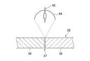
本実施形態の場合、図4に示す装置を用いることができる。本図に示す装置は、少なくとも一つの、ランプ42及び当該ランプ42が出射する光を集光する集光部としての楕円ミラー44を備える。ランプ42としては、赤外線結晶成長装置に一般的に用いられるキセノンランプやハロゲンランプを用いることができる。出力としては1〜30kW程度のものが好ましい。レーザーとしては、波長780〜1600nmの赤外線レーザーを用いることができる。さらに、取り扱いの容易さおよび光源の寿命の観点から、半導体レーザーを複数モジュール化した波長780〜980nm、出力200〜400W程度のパッケージタイプの光源を用いることが好ましい。 In the case of this embodiment, the apparatus shown in FIG. 4 can be used. The apparatus shown in the figure includes at least one
加熱は、突き合わせ面37の外側からであればよく、シリコン部材に対して垂直方向には限られず、斜めからであってもよい。 The heating may be from the outside of the butting
集光領域は、通常直径10〜30mm程度である。集光領域は、ランプ42の発光位置を楕円ミラー44の焦点からずらすことにより、30〜100mm程度に広がる。集光領域が広がることにより、加熱範囲をひろげることができる。集光領域を、突き合わせ面37のリング状部材32における上面の全域に亘って走査させて加熱するのが好ましい。 The condensing region is usually about 10 to 30 mm in diameter. The condensing region is expanded to about 30 to 100 mm by shifting the light emission position of the
まず、楕円ミラー44の焦点位置とランプ42の発光部の位置を合致させるようランプ位置を調整し、シリコン部材の上面の高さを楕円ミラー44のもう一つの焦点位置になるように調整することにより、照射位置での楕円ミラー44の広がりを約3mmとする。この状態で、楕円ミラー44を突き合わせ面37の位置に合わせランプ42のパワーを上げる。加熱を開始すると、突き合わせ面37の上面側が融解してシリコン融解物が生成する。具体的には、ランプ定格の60%で上面が解け始める(表面温度が1420℃と推定される)、ランプ定格の90%で突き合わせ面37の間に、突き合わせ面37で接するシリコンが融解しシリコン融解物が毛細管現象により流れ込んで突き合わせ面37の間の一部を塞ぐ。この状態で、楕円ミラー44を突き合わせ面37に沿って一定の速度、例えば5mm/分の速度で走査することにより、突き合わせ面37の間を融解シリコンで埋め、塞ぐことができる。楕円ミラー44を突き合わせ面37の外縁のうち、リング状部材32における上面側に亘って走査させて加熱する。加えてリング状部材の下面側において突き合わせ面37を同様の方法により加熱してもよい。 First, the lamp position is adjusted so that the focal position of the
次いで、融解した突き合わせ面37の上面を冷却し、シリコン融解物をシリコン部材の結晶に従って結晶化させる。具体的にはシリコン融解物が固まり始めるランプ定格の60%まで2分でランプ42のパワーを下げ、その状態で5分保持する。このときの表面温度は1400℃〜1415℃である。シリコン融解物は、突き合わせ面37で接するシリコン部材の端面の結晶性を引き継いだシリコン接着部39Aとなる。シリコン接着部39Aは、シリコン部材が単結晶の場合、一方のシリコン部材の端面の結晶性を引き継いだ単結晶シリコンからなる一のシリコン接着部と、他方のシリコン部材の端面の結晶性を引き継いだ単結晶シリコンからなる他のシリコン接着部が一体化される。 Next, the upper surface of the
上記の手順によって、全ての突き合わせ面37において、シリコン接着部39Aを同様に形成することにより、第1シリコン部材34,36,38同士を接合し、リング状部材32を形成することができる。 By forming the
上記のようにして得られたリング状部材32は、機械加工により内側の全周に渡って凹部を形成することにより、フォーカスリング18となり得る。 The ring-shaped
リング状部材32は、シリコン製部品の外径より小さいウエハ用シリコン結晶インゴットから切り出した3個以上のシリコン部材を組み合わせて製造することができる。したがってリング状部材32は、シリコン製部品の外径より大きいウエハ用シリコン結晶インゴットを用いる必要がないので、その分コストを低減することができる。 The ring-shaped
本実施形態に係るリング状部材32は、突き合わせ面37がシリコン接着部39Aにより接合されているので、真空チャンバー12内においてプラズマが照射されても、真空チャンバー12内が汚染されることがない。 In the ring-shaped
(3)変形例
本実施形態の場合、突き合わせ面37で接する端面のシリコンを融解し、シリコン接着部39Aを形成する場合について説明したが、本発明はこれに限らない。図5に示すように、突き合わせ面上に、単結晶又は多結晶のシリコン片40を置き、当該シリコン片40を融解してシリコン接着部39Bを形成してもよい。シリコン片40を用いない場合、突き合わせ面37の上面側のシリコンが融解して、突き合わせ面37の間に流れ込むことにより、突き合わせ面37の上面が凹む場合がある。シリコン片40を用いてシリコン接着部39Bを形成することにより、シリコン接着部39Bが形成された後の突き合わせ面37の上面55が、凹むことを防止することができる(図6)。シリコン片40は、突き合わせ面37の間の体積と、同じ体積であることが好ましい。(3) Modification In the case of the present embodiment, the case has been described in which the silicon on the end face that contacts the butting
2.第2実施形態
次に第2実施形態に係るリング状部材について説明する。なお、上記第1実施形態と同様の構成については同様の符号を付し、説明を省略する。図7に示すリング状部材46は、第1リング体35と、第2リング体47とを備える。本図に示す第1リング体35は、第1シリコン部材41,43,45を備え、上記第1実施形態のリング状部材32に比べ幅が小さい点のみが異なる。第2リング体47は、複数(本図の場合3個)の第2シリコン部材48,50,52を備える。第2シリコン部材48,50,52は、説明の便宜上、符号を変えているが、第1シリコン部材41,43,45と同じである。第1リング体35と第2リング体47は、シリコン部材同士の突き合わせ面49が円周方向にずれた状態で接合面54において同軸上に重ねられている。2. Second Embodiment Next, a ring-shaped member according to a second embodiment will be described. In addition, about the structure similar to the said 1st Embodiment, the same code | symbol is attached | subjected and description is abbreviate | omitted. A ring-shaped
図8Aには第1シリコン部材41,43の間の突き合わせ面49、図8Bには第2シリコン部材48,52の間の突き合わせ面49を示している。図中矢印の向きは、リング状部材46の半径方向の外側向きを示す。 8A shows a
第1シリコン部材41,43の間の突き合わせ面49には、第1シリコン接着部51が形成されている(図8A)。第1リング体35と第2リング体47の間の接合面54には、第2シリコン接着部53が形成されている。第2シリコン部材48,52の間の突き合わせ面49には、第1シリコン接着部が設けられていない(図8B)。 A first
このようにして第1シリコン接着部51は、第1シリコン部材41,43,45同士の突き合わせ面49の間、及び第1リング体35と第2リング体47の接合面54の間を塞いでいる。 In this way, the first
次に、本実施形態のリング状部材46の製造方法について説明する。なお、上記第1実施形態と同様の工程については適宜説明を省略する。まず表面処理後の3個の第2シリコン部材48,50,52をリング状に並べる。次いで、第2シリコン部材48,50,52の上面に3個の第1シリコン部材41,43,45を置く。第1シリコン部材41,43,45は、先に配置された第2シリコン部材48,50,52に対し、長手方向の長さの半分だけずらして配置する。上記のようにして、第2シリコン部材48,50,52上に、第1シリコン部材41,43,45が積まれた状態となる。 Next, the manufacturing method of the ring-shaped
次に、第1シリコン部材34,36,38側から加熱して、第1シリコン部材41,43,45同士の突き合わせ面49の間にシリコンの融解物を生成し、第1シリコン接着部51を形成する。加熱条件、冷却条件は、上記第1実施形態と同様とすることができる。 Next, heating is performed from the
次いで、第1リング体35及び第2リング体47の間の接合面54の間のシリコンを加熱して融解する。融解したシリコンは、毛細管現象により水平方向である接合面54の間に流れ込み、第2シリコン接着部53を形成する。 Next, the silicon between the bonding surfaces 54 between the
本実施形態のリング状部材46は、突き合わせ面49の間に第1シリコン接着部51、及び、接合面54の間が第2シリコン接着部53で接合されているので、上記第1実施形態と同様の効果を得ることができる。 Since the ring-shaped
本実施形態の場合、突き合わせ面49で接する端面のシリコンを融解し、第1シリコン接着部51を形成する場合について説明したが、本発明はこれに限らない。上記図5に示したように、突き合わせ面上にシリコン片40を置き、当該シリコン片40を融解して第1シリコン接着部を形成してもよい。 In the case of this embodiment, although the case where the silicon | silicone of the end surface which contact | connects at the butt | matching
本実施形態の場合、上記第1実施形態のリング状部材32に比べ幅が小さい場合について説明したが、本発明はこれに限らない。第1リング体と第2リング体の間の接合面を十分な機械的強度を持つように接合できれば、リング状部材の幅は適宜選択することができる。
第2シリコン部材48,52の間の突き合わせ面49には、第1シリコン接着部を設けていない場合について説明したが、本発明はこれに限らない。第2シリコン部材48,52の間の突き合わせ面49に第1シリコン接着部を設けてもよい。In the case of this embodiment, although the case where a width | variety was small compared with the ring-shaped
Although the case where the first silicon bonding portion is not provided on the butting
3.第3実施形態
次に第2実施形態に係るリング状部材について説明する。図9に示すリング状部材56は、複数(本図の場合、3個)の第1シリコン部材58,60,62と、第1シリコン部材58,60,62同士を跨ぐ位置に埋め込まれた複数(3個)の埋込みシリコン部材64Aとを備える。埋込みシリコン部材64Aは、リング状部材56のプラズマが照射される側と反対側、本図の場合、下面側に設けられる。3. Third Embodiment Next, a ring-shaped member according to a second embodiment will be described. The ring-shaped
埋込みシリコン部材64Aは、シリコン部材と同じ材料で形成されるのが好ましい。埋込みシリコン部材64Aの四隅は、R加工されているのが好ましい。埋込みシリコン部材64Aは、四隅がR加工されていることにより、欠けなどの損傷を防止することができる。Rは、3mm以上であるのが好ましい。 The embedded
埋込みシリコン部材64Aは、下面が、シリコン部材の下面と略同じ高さとなるように形成されるのが好ましい。埋込みシリコン部材64Aの厚さは、シリコン部材の厚さの20〜80%が好ましく、40〜60%がより好ましい。 The embedded
埋込みシリコン部材64Aは、矩形の板状部材からなり、平面視においてリング状部材56から突出しない大きさであるのが好ましい。埋込みシリコン部材64Aの長手方向の長さは、リング状部材56の外周長さの2〜10%であるのが好ましい。 The embedded
より具体的なシリコン部材のサイズは、内周直径340mm、外周直径420mm、厚み4mmのリングを、3分割した大きさとすることができる。埋込みシリコン部材64Aは、長さ60mm、幅25mm、4隅に5mmのR加工を施した厚さ2mmとすることができる。シリコン部材の下面に形成される穴は、シリコンの小片の形状に対応した形状とし、深さは2mmとする。この場合、埋込みシリコン部材64Aの厚さはシリコン部材の厚さの50%、埋込みシリコン部材64Aの長手方向の長さはリング状部材56の外周長さの5%である。 More specifically, the silicon member can be divided into three rings each having an inner diameter of 340 mm, an outer diameter of 420 mm, and a thickness of 4 mm. The embedded
図10に示すように、シリコン部材の下面には、長手方向の端部に、底面を有する穴が形成されている。図10には、第1シリコン部材58,60の間の突き合わせ面63Aを示している。埋込みシリコン部材64Aは、当該穴に埋め込まれる。第1シリコン部材58,60,62同士の突き合わせ面63Aの間には、第1シリコン接着部68が設けられている。埋込みシリコン部材64Aの周縁と、第1シリコン部材58,60,62の穴内面との間には、第2シリコン接着部70が設けられている。 As shown in FIG. 10, a hole having a bottom surface is formed at an end portion in the longitudinal direction on the lower surface of the silicon member. FIG. 10 shows a butting
本実施形態に係る突き合わせ面における第1シリコン接着部68は、上記第1実施形態と同様の方法により、形成することができる。第2シリコン接着部70は、シリコン部材の下面側から埋込みシリコン部材64Aの周縁と第1シリコン部材58,60,62の穴内面の近傍のシリコンを、上記第1実施形態と同様の方法で加熱して、シリコンの融解物を生成することで、形成することができる。 The 1st
本実施形態のリング状部材56は、埋込みシリコン部材64Aを設けたことにより、シリコン部材同士の間の接合面積を大きくすることができるので、機械的強度をより大きくすることができる。また、リング状部材56は、突き合わせ面63Aの間が第1シリコン接着部68で接合されていることにより、上記第1実施形態と同様の効果を得ることができる。 Since the ring-shaped
埋込みシリコン部材64Aは、矩形状である必要はなく、例えば、図11に示すように、長円形状の埋込みシリコン部材64B(図11A)、円弧状の埋込みシリコン部材64C(図11B)でもよい。また埋込みシリコン部材64B,64Cの長手方向端部は、同図に示すように、半円形状でもよい。 The embedded
本実施形態の場合、突き合わせ面63Aで接する端面のシリコンを融解し、第1シリコン接着部68を形成する場合について説明したが、本発明はこれに限らない。図5に示したように、突き合わせ面上にシリコン片40を置き、当該シリコン片40を融解して第1シリコン接着部を形成してもよい。 In the case of this embodiment, although the case where the silicon | silicone of the end surface which contact | abuts with the butting | matching
12 真空チャンバー(処理室)
22 ウエハ(基板)
32 リング状部材
34,36,38 第1シリコン部材(シリコン部材)
37 突き合わせ面
39A,39B シリコン接着部
41,43,45 第1シリコン部材(シリコン部材)
48,50,52 第2シリコン部材(シリコン部材)
49 突き合わせ面
51 第1シリコン接着部(シリコン接着部)
53 第2シリコン接着部(シリコン接着部)
58,60,62 第1シリコン部材(シリコン部材)
63A 突き合わせ面
64A,64B,64C 埋込みシリコン部材
68 第1シリコン接着部(シリコン接着部)
70 第2シリコン接着部(シリコン接着部)12 Vacuum chamber (processing room)
22 Wafer (substrate)
32 Ring-shaped
37 Abutting surfaces 39A, 39B
48, 50, 52 Second silicon member (silicon member)
49
53 Second silicon bonding part (silicon bonding part)
58, 60, 62 First silicon member (silicon member)
63A Butted surfaces 64A, 64B, 64C Embedded
70 Second silicon bonding part (silicon bonding part)
Claims (6)
Translated fromJapanese一のシリコン部材の一の突き合わせ面と、他のシリコン部材の他の突き合わせ面とが、突き合わされるように配置する工程と、
前記一の突き合わせ面と前記他の突き合わせ面とをキセノンランプ又はハロゲンランプにより行われる光加熱により加熱し、前記一の突き合わせ面の表面のシリコンと前記他の突き合わせ面の表面のシリコンとを融解し、前記一の突き合わせ面と前記他の突き合わせ面との間にシリコン融解物が流れ込むようにする工程と、
前記一の突き合わせ面と前記他の突き合わせ面とを冷却し、前記シリコン融解物を結晶化させてシリコン接着部を形成し、前記一のシリコン部材と前記他のシリコン部材とを前記シリコン接着部を介して接合する工程と
を含むことを特徴とするリング状部材の製造方法。A method of manufacturing a ring-shaped member installed in a processing chamber in which the substrate of a substrate processing apparatus that performs plasma processing on a substrate is accommodated,
Disposing the one butting surface of the one silicon member and the other butting surface of the other silicon member so as to be butted, and
The one butted surface and the other butted surfaceare heated by light heatingperformed by a xenon lamp or a halogen lamp, and the silicon on the surface of the one butted surface and the silicon on the surface of the other butted surface are melted. Allowing the silicon melt to flow between the one butting surface and the other butting surface;
The one butted surface and the other butted surface are cooled, the silicon melt is crystallized to form a silicon bonded portion, and the one silicon member and the other silicon member are bonded to the silicon bonded portion. A method of manufacturing a ring-shaped member.
一のシリコン部材の一の突き合わせ面と、他のシリコン部材の他の突き合わせ面とが、隙間を介して突き合わされるように配置する工程と、A step of disposing the one butting surface of one silicon member and the other butting surface of the other silicon member so as to be butted via a gap;
前記一の突き合わせ面と前記他の突き合わせ面とを光加熱により加熱し、前記一の突き合わせ面の表面のシリコンと前記他の突き合わせ面の表面のシリコンとを融解し接触させ、前記一の突き合わせ面と前記他の突き合わせ面との間の前記隙間にシリコン融解物が毛細管現象により流れ込むようにする工程と、The one butting surface and the other butting surface are heated by light heating, and the silicon on the surface of the one butting surface and the silicon on the surface of the other butting surface are melted and brought into contact with each other. And allowing the silicon melt to flow into the gap between the other butted surfaces by capillary action;
前記一の突き合わせ面と前記他の突き合わせ面とを冷却し、前記シリコン融解物を結晶化させてシリコン接着部を形成し、前記一のシリコン部材と前記他のシリコン部材とを前記シリコン接着部を介して接合する工程とThe one butted surface and the other butted surface are cooled, the silicon melt is crystallized to form a silicon bonded portion, and the one silicon member and the other silicon member are bonded to the silicon bonded portion. And joining process via
を含むことを特徴とするリング状部材の製造方法。The manufacturing method of the ring-shaped member characterized by including.
複数のシリコン部材と、
一の前記シリコン部材の一の突き合わせ面と他の前記シリコン部材の他の突き合わせ面との間の隙間を埋めるように設けられ、前記一の突き合わせ面と前記他の突き合わせ面とを接合するシリコン接着部とを備え、
前記シリコン接着部は、前記一の前記シリコン部材の端面のシリコン融解物と前記他の前記シリコン部材の端面のシリコン融解物とが接触し毛細管現象により前記隙間に流れ込み結晶化したものであり、前記一の突き合わせ面の結晶性を引き継いだ単結晶シリコンからなる一のシリコン接着部と前記他の突き合わせ面の結晶性を引き継いだ単結晶シリコンからなる他のシリコン接着部とが原子レベルで一体化されている
ことを特徴とするリング状部材。A ring-shaped member installed in a processing chamber in which the substrate of a substrate processing apparatus that performs plasma processing on the substrate is accommodated,
A plurality of silicon members;
Silicon bondingthat is provided so as to fill a gap between one butting surface of one silicon memberand another butting surfaceof another silicon member, and bonds theone butting surface and the other butting surface With
The silicon adhesion portion is acrystal where the silicon melt on the end face of the one silicon member and the silicon melt on the end face of the other silicon member come into contact with each other and flow into the gap by capillary action, and are crystallized. integratedin one silicone-adhering portionand the front SL other abutting surfaces other silicone-adhering portion and theatomic level of monocrystalline silicon takes over the crystallinity of the monocrystalline silicon takes over the crystallinity of the first abutting surface A ring-shaped member characterized by being made.
Priority Applications (9)
| Application Number | Priority Date | Filing Date | Title |
|---|---|---|---|
| JP2017100173AJP6278498B1 (en) | 2017-05-19 | 2017-05-19 | Ring-shaped member manufacturing method and ring-shaped member |
| CN201880002209.8ACN109287126B (en) | 2017-05-19 | 2018-03-07 | Method for manufacturing annular member and annular member |
| US16/307,849US10984988B2 (en) | 2017-05-19 | 2018-03-07 | Method of manufacturing ring-shaped member and ring-shaped member |
| PCT/JP2018/008870WO2018211788A1 (en) | 2017-05-19 | 2018-03-07 | Method for manufacturing annular member and annular member |
| EP18802750.2AEP3454361B1 (en) | 2017-05-19 | 2018-03-07 | Method for manufacturing annular member and annular member |
| KR1020187034663AKR102214968B1 (en) | 2017-05-19 | 2018-03-07 | Ring-shaped member manufacturing method and ring-shaped member |
| SG11201810732UASG11201810732UA (en) | 2017-05-19 | 2018-03-07 | Method for manufacturing annular member and annular member |
| TW107108692ATWI765004B (en) | 2017-05-19 | 2018-03-14 | Method for manufacturing ring-shaped member, and ring-shaped member |
| US17/207,693US11551915B2 (en) | 2017-05-19 | 2021-03-21 | Method of manufacturing ring-shaped member and ring-shaped member |
Applications Claiming Priority (1)
| Application Number | Priority Date | Filing Date | Title |
|---|---|---|---|
| JP2017100173AJP6278498B1 (en) | 2017-05-19 | 2017-05-19 | Ring-shaped member manufacturing method and ring-shaped member |
Publications (2)
| Publication Number | Publication Date |
|---|---|
| JP6278498B1true JP6278498B1 (en) | 2018-02-14 |
| JP2018195764A JP2018195764A (en) | 2018-12-06 |
Family
ID=61195744
Family Applications (1)
| Application Number | Title | Priority Date | Filing Date |
|---|---|---|---|
| JP2017100173AActiveJP6278498B1 (en) | 2017-05-19 | 2017-05-19 | Ring-shaped member manufacturing method and ring-shaped member |
Country Status (8)
| Country | Link |
|---|---|
| US (2) | US10984988B2 (en) |
| EP (1) | EP3454361B1 (en) |
| JP (1) | JP6278498B1 (en) |
| KR (1) | KR102214968B1 (en) |
| CN (1) | CN109287126B (en) |
| SG (1) | SG11201810732UA (en) |
| TW (1) | TWI765004B (en) |
| WO (1) | WO2018211788A1 (en) |
Families Citing this family (2)
| Publication number | Priority date | Publication date | Assignee | Title |
|---|---|---|---|---|
| CN114388324B (en)* | 2020-10-22 | 2025-05-09 | 中微半导体设备(上海)股份有限公司 | A grounding ring and plasma etching equipment |
| JP7725098B1 (en)* | 2024-03-04 | 2025-08-19 | 日本新工芯技株式会社 | Silicon bonded body manufacturing apparatus and silicon bonded body manufacturing method |
Citations (2)
| Publication number | Priority date | Publication date | Assignee | Title |
|---|---|---|---|---|
| JP2003257807A (en)* | 2002-03-07 | 2003-09-12 | Shin Etsu Chem Co Ltd | Method of manufacturing silicon processed product and silicon processed product |
| JP2010114313A (en)* | 2008-11-07 | 2010-05-20 | Tokyo Electron Ltd | Ring-shaped member and method for manufacturing same |
Family Cites Families (19)
| Publication number | Priority date | Publication date | Assignee | Title |
|---|---|---|---|---|
| EP0615431A4 (en)* | 1992-08-27 | 1995-04-19 | Craig John Hubbard | An ankle brace. |
| JP2907375B2 (en)* | 1994-04-21 | 1999-06-21 | 古河電気工業株式会社 | Dust proof ring for conduit air cable connection |
| US7083694B2 (en)* | 2003-04-23 | 2006-08-01 | Integrated Materials, Inc. | Adhesive of a silicon and silica composite particularly useful for joining silicon parts |
| US7074693B2 (en)* | 2003-06-24 | 2006-07-11 | Integrated Materials, Inc. | Plasma spraying for joining silicon parts |
| TW200520632A (en)* | 2003-09-05 | 2005-06-16 | Tokyo Electron Ltd | Focus ring and plasma processing apparatus |
| JP5110772B2 (en)* | 2004-02-03 | 2012-12-26 | 株式会社半導体エネルギー研究所 | Manufacturing method of substrate having semiconductor thin film layer |
| KR100684544B1 (en)* | 2005-07-15 | 2007-02-20 | 호서대학교 산학협력단 | Stress measuring device of wafer in high temperature processing |
| JP5154124B2 (en) | 2007-03-29 | 2013-02-27 | 東京エレクトロン株式会社 | Plasma processing equipment |
| JP5424445B2 (en)* | 2007-06-12 | 2014-02-26 | 国立大学法人京都工芸繊維大学 | Semiconductor substrate manufacturing method and semiconductor substrate |
| US8679288B2 (en)* | 2008-06-09 | 2014-03-25 | Lam Research Corporation | Showerhead electrode assemblies for plasma processing apparatuses |
| KR101017160B1 (en)* | 2008-06-17 | 2011-02-25 | 주식회사 동부하이텍 | How to form fluorine diffusion barrier |
| KR101041947B1 (en)* | 2008-12-23 | 2011-06-15 | 청주대학교 산학협력단 | SIO thin film heat treatment apparatus |
| WO2010150590A1 (en)* | 2009-06-24 | 2010-12-29 | キヤノンアネルバ株式会社 | Vacuum heating/cooling apparatus and method of producing magnetoresistive element |
| JP5952550B2 (en)* | 2011-11-28 | 2016-07-13 | 株式会社半導体エネルギー研究所 | Bonding device |
| JP5955658B2 (en)* | 2012-06-15 | 2016-07-20 | 株式会社Screenホールディングス | Heat treatment method and heat treatment apparatus |
| WO2014034180A1 (en)* | 2012-08-28 | 2014-03-06 | 株式会社リケン | Piston ring |
| TWM464809U (en)* | 2012-10-20 | 2013-11-01 | Applied Materials Inc | Focus ring segment and assembly |
| TW201432826A (en)* | 2013-02-01 | 2014-08-16 | Chipbond Technology Corp | Semiconductor packaging process and structure thereof |
| JP5615454B1 (en)* | 2014-02-25 | 2014-10-29 | コバレントマテリアル株式会社 | Focus ring |
- 2017
- 2017-05-19JPJP2017100173Apatent/JP6278498B1/enactiveActive
- 2018
- 2018-03-07CNCN201880002209.8Apatent/CN109287126B/enactiveActive
- 2018-03-07WOPCT/JP2018/008870patent/WO2018211788A1/ennot_activeCeased
- 2018-03-07EPEP18802750.2Apatent/EP3454361B1/enactiveActive
- 2018-03-07KRKR1020187034663Apatent/KR102214968B1/enactiveActive
- 2018-03-07USUS16/307,849patent/US10984988B2/enactiveActive
- 2018-03-07SGSG11201810732UApatent/SG11201810732UA/enunknown
- 2018-03-14TWTW107108692Apatent/TWI765004B/enactive
- 2021
- 2021-03-21USUS17/207,693patent/US11551915B2/enactiveActive
Patent Citations (2)
| Publication number | Priority date | Publication date | Assignee | Title |
|---|---|---|---|---|
| JP2003257807A (en)* | 2002-03-07 | 2003-09-12 | Shin Etsu Chem Co Ltd | Method of manufacturing silicon processed product and silicon processed product |
| JP2010114313A (en)* | 2008-11-07 | 2010-05-20 | Tokyo Electron Ltd | Ring-shaped member and method for manufacturing same |
Non-Patent Citations (1)
| Title |
|---|
| J.C.BEAN, 他: "Epitaxial laser crystallization of thin-film amorphous silicon", APPLIED PHYSICS LETTERS, vol. 33, no. 3, JPN7017003150, 1 August 1978 (1978-08-01), US, pages 227 - 230* |
Also Published As
| Publication number | Publication date |
|---|---|
| CN109287126B (en) | 2021-11-09 |
| TW201902307A (en) | 2019-01-01 |
| CN109287126A (en) | 2019-01-29 |
| KR20190002635A (en) | 2019-01-08 |
| EP3454361B1 (en) | 2021-05-26 |
| SG11201810732UA (en) | 2018-12-28 |
| EP3454361A1 (en) | 2019-03-13 |
| TWI765004B (en) | 2022-05-21 |
| US11551915B2 (en) | 2023-01-10 |
| WO2018211788A1 (en) | 2018-11-22 |
| US20210225617A1 (en) | 2021-07-22 |
| JP2018195764A (en) | 2018-12-06 |
| KR102214968B1 (en) | 2021-02-09 |
| US10984988B2 (en) | 2021-04-20 |
| US20190259581A1 (en) | 2019-08-22 |
| EP3454361A4 (en) | 2020-03-11 |
Similar Documents
| Publication | Publication Date | Title |
|---|---|---|
| US11551915B2 (en) | Method of manufacturing ring-shaped member and ring-shaped member | |
| US10553405B2 (en) | Ring-shaped electrode | |
| US11348764B2 (en) | Electrode ring | |
| US11380525B2 (en) | Ring for electrode | |
| JP6270191B1 (en) | Protective ring | |
| US10580621B2 (en) | Electrode Plate | |
| JP6176620B1 (en) | Ring for electrode |
Legal Events
| Date | Code | Title | Description |
|---|---|---|---|
| A621 | Written request for application examination | Free format text:JAPANESE INTERMEDIATE CODE: A621 Effective date:20170810 | |
| A871 | Explanation of circumstances concerning accelerated examination | Free format text:JAPANESE INTERMEDIATE CODE: A871 Effective date:20170810 | |
| A975 | Report on accelerated examination | Free format text:JAPANESE INTERMEDIATE CODE: A971005 Effective date:20170925 | |
| A131 | Notification of reasons for refusal | Free format text:JAPANESE INTERMEDIATE CODE: A131 Effective date:20171003 | |
| A521 | Request for written amendment filed | Free format text:JAPANESE INTERMEDIATE CODE: A523 Effective date:20171128 | |
| TRDD | Decision of grant or rejection written | ||
| A01 | Written decision to grant a patent or to grant a registration (utility model) | Free format text:JAPANESE INTERMEDIATE CODE: A01 Effective date:20171226 | |
| A61 | First payment of annual fees (during grant procedure) | Free format text:JAPANESE INTERMEDIATE CODE: A61 Effective date:20180111 | |
| R150 | Certificate of patent or registration of utility model | Ref document number:6278498 Country of ref document:JP Free format text:JAPANESE INTERMEDIATE CODE: R150 | |
| R250 | Receipt of annual fees | Free format text:JAPANESE INTERMEDIATE CODE: R250 | |
| R250 | Receipt of annual fees | Free format text:JAPANESE INTERMEDIATE CODE: R250 |