JP6272873B2 - Selective etching of silicon carbonitride - Google Patents
Selective etching of silicon carbonitrideDownload PDFInfo
- Publication number
- JP6272873B2 JP6272873B2JP2015533083AJP2015533083AJP6272873B2JP 6272873 B2JP6272873 B2JP 6272873B2JP 2015533083 AJP2015533083 AJP 2015533083AJP 2015533083 AJP2015533083 AJP 2015533083AJP 6272873 B2JP6272873 B2JP 6272873B2
- Authority
- JP
- Japan
- Prior art keywords
- region
- plasma
- nitrogen
- carbon
- fluorine
- Prior art date
- Legal status (The legal status is an assumption and is not a legal conclusion. Google has not performed a legal analysis and makes no representation as to the accuracy of the status listed.)
- Expired - Fee Related
Links
Images


Classifications
- H—ELECTRICITY
- H01—ELECTRIC ELEMENTS
- H01L—SEMICONDUCTOR DEVICES NOT COVERED BY CLASS H10
- H01L21/00—Processes or apparatus adapted for the manufacture or treatment of semiconductor or solid state devices or of parts thereof
- H01L21/02—Manufacture or treatment of semiconductor devices or of parts thereof
- H01L21/04—Manufacture or treatment of semiconductor devices or of parts thereof the devices having potential barriers, e.g. a PN junction, depletion layer or carrier concentration layer
- H01L21/18—Manufacture or treatment of semiconductor devices or of parts thereof the devices having potential barriers, e.g. a PN junction, depletion layer or carrier concentration layer the devices having semiconductor bodies comprising elements of Group IV of the Periodic Table or AIIIBV compounds with or without impurities, e.g. doping materials
- H01L21/30—Treatment of semiconductor bodies using processes or apparatus not provided for in groups H01L21/20 - H01L21/26
- H01L21/31—Treatment of semiconductor bodies using processes or apparatus not provided for in groups H01L21/20 - H01L21/26 to form insulating layers thereon, e.g. for masking or by using photolithographic techniques; After treatment of these layers; Selection of materials for these layers
- H01L21/3105—After-treatment
- H01L21/311—Etching the insulating layers by chemical or physical means
- H01L21/31105—Etching inorganic layers
- H01L21/31111—Etching inorganic layers by chemical means
- H01L21/31116—Etching inorganic layers by chemical means by dry-etching
- H—ELECTRICITY
- H01—ELECTRIC ELEMENTS
- H01J—ELECTRIC DISCHARGE TUBES OR DISCHARGE LAMPS
- H01J37/00—Discharge tubes with provision for introducing objects or material to be exposed to the discharge, e.g. for the purpose of examination or processing thereof
- H01J37/32—Gas-filled discharge tubes
- H01J37/32009—Arrangements for generation of plasma specially adapted for examination or treatment of objects, e.g. plasma sources
- H01J37/32357—Generation remote from the workpiece, e.g. down-stream
- H—ELECTRICITY
- H01—ELECTRIC ELEMENTS
- H01L—SEMICONDUCTOR DEVICES NOT COVERED BY CLASS H10
- H01L21/00—Processes or apparatus adapted for the manufacture or treatment of semiconductor or solid state devices or of parts thereof
- H01L21/70—Manufacture or treatment of devices consisting of a plurality of solid state components formed in or on a common substrate or of parts thereof; Manufacture of integrated circuit devices or of parts thereof
- H01L21/71—Manufacture of specific parts of devices defined in group H01L21/70
- H01L21/768—Applying interconnections to be used for carrying current between separate components within a device comprising conductors and dielectrics
- H01L21/76801—Applying interconnections to be used for carrying current between separate components within a device comprising conductors and dielectrics characterised by the formation and the after-treatment of the dielectrics, e.g. smoothing
- H01L21/76802—Applying interconnections to be used for carrying current between separate components within a device comprising conductors and dielectrics characterised by the formation and the after-treatment of the dielectrics, e.g. smoothing by forming openings in dielectrics
Landscapes
- Engineering & Computer Science (AREA)
- Chemical & Material Sciences (AREA)
- Physics & Mathematics (AREA)
- General Physics & Mathematics (AREA)
- Condensed Matter Physics & Semiconductors (AREA)
- Manufacturing & Machinery (AREA)
- Computer Hardware Design (AREA)
- Microelectronics & Electronic Packaging (AREA)
- Power Engineering (AREA)
- Chemical Kinetics & Catalysis (AREA)
- General Chemical & Material Sciences (AREA)
- Inorganic Chemistry (AREA)
- Plasma & Fusion (AREA)
- Analytical Chemistry (AREA)
- Drying Of Semiconductors (AREA)
Description
Translated fromJapanese関連出願の相互参照
本出願は、あらゆる目的において参照によりその全体が本明細書に組み込まれる、2012年9月20日に出願された、「SILICON−CARBON−NITRIDE SELECTIVE ETCH」なる名称の、米国特許仮出願第61/703,612号の利益を主張する。CROSS REFERENCE TO RELATED APPLICATIONS This application is a U.S. patent entitled “SILICON-CARBON-NITRIDE SELECTION ETCH” filed on September 20, 2012, which is incorporated herein by reference in its entirety for all purposes. Claims the benefit of provisional application 61 / 703,612.
集積回路は、複雑にパターン形成された材料層を基板表面上に製作するプロセスにより、可能になる。パターン形成された材料を基板上に製作することは、露出された材料の除去のための制御された方法を必要とする。化学エッチングが、フォトレジストの中のパターンを下層の中へ転写すること、層を薄くすること、又は表面上にすでに存在する特徴の横寸法を細くすることを含む種々の目的のために用いられる。一つの材料を別の材料より速くエッチングして、例えば、パターン転写プロセスが進行するのを助ける、エッチングプロセスがあることが、しばしば望ましい。そのようなエッチングプロセスは、第一の材料に対して選択的であると言われる。材料、回路及びプロセスの多様性の結果として、種々の材料に対して選択性を持ったエッチングプロセスが開発されて来た。しかしながら、炭窒化ケイ素を選択的にエッチングするための選択肢は、ほとんどない。 Integrated circuits are made possible by the process of fabricating a complex patterned material layer on the substrate surface. Fabricating patterned material on a substrate requires a controlled method for removal of exposed material. Chemical etching is used for a variety of purposes including transferring the pattern in the photoresist into the underlying layer, thinning the layer, or thinning the lateral dimensions of features already present on the surface . It is often desirable to have an etching process that etches one material faster than another, for example, to help the pattern transfer process proceed. Such an etching process is said to be selective for the first material. As a result of the diversity of materials, circuits and processes, etching processes with selectivity for various materials have been developed. However, there are few options for selectively etching silicon carbonitride.
ドライエッチングプロセスは、半導体基板から材料を選択的に除去するために、しばしば望ましい。望ましさは、物理的な乱れを最小にして、微小構造から材料を穏やかに除去する能力から生じる。ドライエッチングプロセスはまた、気相試薬を除去することにより、エッチング速度が、突然に止められることを可能にする。いくつかのドライエッチングプロセスは、一つ又は複数の前駆体から形成される遠隔プラズマ副生成物への基板の曝露を含む。例えば、アンモニア及び三フッ化窒素の遠隔プラズマ励起は、プラズマ流出物が基板処理領域の中に流されるときに、酸化ケイ素がパターン形成された基板から選択的に除去されることを可能にする。いくつかの選択的遠隔プラズマエッチングプロセスは、基板材料が除去されるにつれて基板の表面上で成長する固体副生成物を生じる。その後、固体副生成物は、基板の温度が上げられるときに、昇華によって除去される。固体副生成物の生成の結果として、Siconi(商標)エッチング処理は、エッチングされる材料の露出された領域の中に又は近くに形成される、精緻な残りの構造を変形させる可能性がある。 A dry etch process is often desirable to selectively remove material from a semiconductor substrate. The desirability arises from the ability to gently remove material from the microstructure with minimal physical disturbance. The dry etch process also allows the etch rate to be abruptly stopped by removing the gas phase reagent. Some dry etching processes involve exposure of the substrate to a remote plasma byproduct formed from one or more precursors. For example, remote plasma excitation of ammonia and nitrogen trifluoride allows silicon oxide to be selectively removed from the patterned substrate as the plasma effluent is flowed into the substrate processing region. Some selective remote plasma etching processes produce solid byproducts that grow on the surface of the substrate as the substrate material is removed. Thereafter, the solid by-product is removed by sublimation when the temperature of the substrate is raised. As a result of the formation of solid byproducts, the Siconi ™ etching process can deform the fine remaining structure that forms in or near the exposed areas of the material being etched.
理想的には固体副生成物を形成することなく、炭窒化ケイ素を選択的に除去する気相方法。 A gas phase process that selectively removes silicon carbonitride, ideally without forming solid by-products.
パターン形成されたヘテロジニアス構造上の露出されたケイ素‐窒素‐及び炭素含有材料をエッチングする方法が、記載され、本方法は、フッ素含有前駆体及び酸素含有前駆体から形成される遠隔プラズマエッチングを含む。遠隔プラズマからのプラズマ流出物が、基板処理領域の中に流され、そこでプラズマ流出物は、ケイ素‐窒素‐及び炭素含有材料の露出された領域と反応する。プラズマ流出物は、パターン形成されたヘテロジニアス構造と反応し、露出されたケイ素‐窒素‐及び炭素含有材料領域からケイ素‐窒素‐及び炭素含有材料を選択的に除去する一方、選択された他の露出された材料を非常にゆっくりと除去する。ケイ素‐窒素‐及び炭素含有材料の選択性は、遠隔プラズマと基板処理領域の間に配置されるイオン抑制要素の存在に、一部は起因する。イオン抑制要素は、基板に到達するイオン性荷電種の数を制御する。本方法は、露出された酸化ケイ素又は露出された窒化ケイ素より速い速度でケイ素‐窒素‐及び炭素含有材料を選択的に除去するために用いられうる。 A method for etching exposed silicon-nitrogen- and carbon-containing material on a patterned heterogeneous structure is described, the method comprising remote plasma etching formed from a fluorine-containing precursor and an oxygen-containing precursor. Including. Plasma effluent from a remote plasma is flowed into the substrate processing region where the plasma effluent reacts with exposed regions of silicon-nitrogen- and carbon-containing materials. The plasma effluent reacts with the patterned heterogeneous structure, selectively removing silicon-nitrogen- and carbon-containing materials from the exposed silicon-nitrogen- and carbon-containing material regions, while selecting other Remove exposed material very slowly. The selectivity of silicon-nitrogen- and carbon-containing materials is due in part to the presence of ion suppression elements located between the remote plasma and the substrate processing region. The ion suppression element controls the number of ionic charged species that reach the substrate. The method can be used to selectively remove silicon-nitrogen- and carbon-containing materials at a faster rate than exposed silicon oxide or exposed silicon nitride.
本発明の実施形態は、基板処理チャンバの基板処理領域の中でパターン形成された基板をエッチングする方法を含む。パターン形成された基板は、露出されたケイ素‐窒素‐及び炭素含有領域を有する。本方法は、プラズマ流出物を作るためにプラズマ領域の中でプラズマを形成している間、基板処理領域と流体結合した遠隔プラズマ領域の中にフッ素含有前駆体及び酸素含有前駆体の各々を流すことを含む。本方法は、シャワーヘッドの中の貫通孔を通してプラズマ流出物を基板処理領域の中に流すことにより、露出されたケイ素‐窒素‐及び炭素含有領域をエッチングすることを、更に含む。 Embodiments of the invention include a method for etching a patterned substrate in a substrate processing region of a substrate processing chamber. The patterned substrate has exposed silicon-nitrogen- and carbon-containing regions. The method flows each of the fluorine-containing precursor and the oxygen-containing precursor into a remote plasma region fluidly coupled to the substrate processing region while forming a plasma in the plasma region to create a plasma effluent. Including that. The method further includes etching the exposed silicon-nitrogen- and carbon-containing regions by flowing plasma effluent through the through holes in the showerhead and into the substrate processing region.
追加の実施形態及び特徴が、一部は以下の記載中に述べられ、そして、一部は、明細書の検討により当業者に明らかとなるであろうし、又は、開示される実施形態の実践により分かるかもしれない。開示される実施形態の特徴及び利点は、本明細書に記載される手段、組合せ、及び方法によって、実現され、達成されうる。 Additional embodiments and features will be set forth in part in the following description and in part will be apparent to those of ordinary skill in the art upon review of the specification or by practice of the disclosed embodiments. You may understand. The features and advantages of the disclosed embodiments may be realized and attained by means of the instrumentalities, combinations, and methods described herein.
開示される実施形態の特徴と利点についての更なる理解が、明細書の残りの部分と図面を参照することにより、実現されうる。 A further understanding of the features and advantages of the disclosed embodiments may be realized by reference to the remaining portions of the specification and the drawings.
添付の図において、類似の構成要素及び/又は特徴は、同じ参照ラベルを持ちうる。更に、同じタイプの種々の構成要素は、ダッシュ及び類似の構成要素の間を区別する第二のラベルが参照ラベルの後に来ることにより、区別されうる。第一の参照ラベルのみが明細書の中で用いられるならば、その記載は、第二の参照ラベルに関わりなく、同じ第一の参照ラベルを持つ類似の構成要素の任意のものに対して適用可能である。 In the appended figures, similar components and / or features may have the same reference label. In addition, various components of the same type can be distinguished by a second label following the reference label that distinguishes between dashes and similar components. If only the first reference label is used in the specification, the description applies to any of the similar components having the same first reference label, regardless of the second reference label. Is possible.
パターン形成されたヘテロジニアス構造上の露出されたケイ素‐窒素‐及び炭素含有材料をエッチングする方法が、記載され、本方法は、フッ素含有前駆体及び酸素含有前駆体から形成される遠隔プラズマエッチングを含む。遠隔プラズマからのプラズマ流出物が、基板処理領域の中に流され、そこでプラズマ流出物は、ケイ素‐窒素‐及び炭素含有材料の露出された領域と反応する。プラズマ流出物は、パターン形成されたヘテロジニアス構造と反応し、露出されたケイ素‐窒素‐及び炭素含有材料領域からケイ素‐窒素‐及び炭素含有材料を選択的に除去する一方、選択された他の露出された材料を非常にゆっくりと除去する。ケイ素‐窒素‐及び炭素含有材料の選択性は、遠隔プラズマと基板処理領域の間に配置されるイオン抑制要素の存在に、一部は起因する。イオン抑制要素は、基板に到達するイオン性荷電種の数を制御する。本方法は、露出された酸化ケイ素又は露出された窒化ケイ素より速い速度でケイ素‐窒素‐及び炭素含有材料を選択的に除去するために用いられうる。 A method for etching exposed silicon-nitrogen- and carbon-containing material on a patterned heterogeneous structure is described, the method comprising remote plasma etching formed from a fluorine-containing precursor and an oxygen-containing precursor. Including. Plasma effluent from a remote plasma is flowed into the substrate processing region where the plasma effluent reacts with exposed regions of silicon-nitrogen- and carbon-containing materials. The plasma effluent reacts with the patterned heterogeneous structure, selectively removing silicon-nitrogen- and carbon-containing materials from the exposed silicon-nitrogen- and carbon-containing material regions, while selecting other Remove exposed material very slowly. The selectivity of silicon-nitrogen- and carbon-containing materials is due in part to the presence of ion suppression elements located between the remote plasma and the substrate processing region. The ion suppression element controls the number of ionic charged species that reach the substrate. The method can be used to selectively remove silicon-nitrogen- and carbon-containing materials at a faster rate than exposed silicon oxide or exposed silicon nitride.
イオン抑制要素は、プラズマ発生領域から基板へと進むイオン性荷電種を減少又は除去するように機能する。無電荷の中性及びラジカル種は、イオンサプレッサの中の開口を通過して、基板で反応しうる。基板の周囲の反応領域の中のイオン性荷電種の完全な除去が、常に望まれる目標とは限らないということに、留意すべきである。多くの場合、エッチング及び/又は堆積プロセスを行なうために、イオン種が基板に到達することが必要とされる。これらの場合、イオンサプレッサは、プロセスを促進する水準に反応領域の中のイオン種の濃度を制御するのに助けとなる。 The ion suppression element functions to reduce or eliminate ionic charged species traveling from the plasma generation region to the substrate. Uncharged neutral and radical species can react with the substrate through an opening in the ion suppressor. It should be noted that complete removal of ionic charged species in the reaction zone around the substrate is not always a desired goal. In many cases, ionic species are required to reach the substrate in order to perform an etching and / or deposition process. In these cases, the ion suppressor helps to control the concentration of ionic species in the reaction zone to a level that facilitates the process.
本発明のいくつかの実施形態に従って、例示的設備のセクションに記載されているようなイオンサプレッサが、基板を選択的にエッチングするためにラジカル及び/又は中性種を供給するために用いられうる。一つの実施形態において、例えば、イオンサプレッサは、ケイ素‐窒素‐及び炭素含有材料を選択的にエッチングするために、フッ素及び酸素含有プラズマ流出物を供給するために、用いられる。プラズマ流出物を用いて、酸化ケイ素に対するケイ素‐窒素‐及び炭素含有材料の、約4000:1ほどに高い又はそれ以上のエッチング速度の選択性が獲得できる。イオンサプレッサは、イオンよりラジカルの濃度が高い反応ガスを供給するために、用いられうる。プラズマの荷電粒子の大部分が、イオンサプレッサにより濾過又は除去されるので、基板は、エッチングプロセスの間、通常バイアスされない。ラジカル及び他の中性種を用いるそのようなプロセスは、スパッタリング及びボンバードメントを含む従来のプラズマエッチングプロセスと比較して、プラズマ損傷を減少させることができる。本発明の実施形態はまた、液体の表面張力が、小さい特徴の曲げ及び剥離を引き起こすことがありうる、従来の湿式エッチングプロセスより有利である。 In accordance with some embodiments of the present invention, an ion suppressor as described in the exemplary equipment section can be used to supply radicals and / or neutral species to selectively etch the substrate. . In one embodiment, for example, an ion suppressor is used to provide fluorine and oxygen-containing plasma effluents to selectively etch silicon-nitrogen- and carbon-containing materials. Using plasma effluents, selectivity of silicon-nitrogen- and carbon-containing materials with respect to silicon oxide can be as high as about 4000: 1 or higher. An ion suppressor can be used to supply a reactive gas having a higher concentration of radicals than ions. Since most of the charged particles of the plasma are filtered or removed by the ion suppressor, the substrate is not normally biased during the etching process. Such processes using radicals and other neutral species can reduce plasma damage compared to conventional plasma etching processes including sputtering and bombardment. Embodiments of the present invention are also advantageous over conventional wet etching processes where the surface tension of the liquid can cause minor feature bending and delamination.
本発明をよりよく理解し、評価するために、開示される実施形態による、炭化ケイ素の選択的エッチングプロセスのフローチャートである、図1への参照が次になされる。炭窒化ケイ素は、ケイ素‐窒素‐及び炭素含有材料の一例である。最初の作業の前に、構造が、パターン形成された基板の中に形成される。構造は、炭窒化ケイ素及び酸化ケイ素の別々の露出された領域を持つ。基板は、その後、処理領域の中へ供給される(作業110)。 To better understand and evaluate the present invention, reference is now made to FIG. 1, which is a flow chart of a selective etching process of silicon carbide according to disclosed embodiments. Silicon carbonitride is an example of a silicon-nitrogen- and carbon-containing material. Prior to the first operation, a structure is formed in the patterned substrate. The structure has separate exposed regions of silicon carbonitride and silicon oxide. The substrate is then fed into the processing area (operation 110).
三フッ化窒素の流れが、処理領域とは別のプラズマ領域の中へ導入される(作業120)。他のフッ素源が、三フッ化窒素を強化する又は代替するために、用いられうる。概して、フッ素含有前駆体が、プラズマ領域の中に流されることができ、該フッ素含有前駆体は、原子状フッ素、二原子フッ素、三フッ化臭素、三フッ化塩素、三フッ化窒素、フッ化水素、六フッ化硫黄及び二フッ化キセノンからなる群から選択される少なくとも一つの前駆体を含む。四フッ化炭素、トリフルオロメタン、ジフルオロメタン、フルオロメタン、等などの炭素含有前駆体さえも、すでに列挙された群に追加されることができる。炭素含有前駆体の使用は、本明細書に記載される酸素含有前駆体の流量の増加を、概して必要とする。分離されたプラズマ領域は、本明細書中で遠隔プラズマ領域と呼ばれることもあり、そして、処理チャンバとは異なるモジュールの中にあってよく、又は処理チャンバ内の区画の中にあってもよい。酸素(O2)もまた、プラズマ領域の中に流され(作業125)、そこで、三フッ化窒素とともにプラズマの中で同時に励起される。概して、酸素含有前駆体が、プラズマ領域の中に流されることができ、該酸素含有前駆体は、O2、O3、N2O、NO、NO2、等から選択される少なくとも一つの前駆体を含みうる。A stream of nitrogen trifluoride is introduced into a plasma region separate from the processing region (operation 120). Other fluorine sources can be used to enhance or replace nitrogen trifluoride. In general, a fluorine-containing precursor can be flowed into the plasma region, the fluorine-containing precursor being atomic fluorine, diatomic fluorine, bromine trifluoride, chlorine trifluoride, nitrogen trifluoride, fluorine. At least one precursor selected from the group consisting of hydrogen fluoride, sulfur hexafluoride and xenon difluoride. Even carbon-containing precursors such as carbon tetrafluoride, trifluoromethane, difluoromethane, fluoromethane, etc. can be added to the groups already listed. The use of carbon-containing precursors generally requires an increase in the flow rate of the oxygen-containing precursor described herein. The separated plasma region may be referred to herein as a remote plasma region and may be in a different module than the processing chamber or may be in a compartment within the processing chamber. Oxygen (O2 ) is also flowed into the plasma region (operation 125) where it is simultaneously excited in the plasma along with nitrogen trifluoride. In general, an oxygen-containing precursor can be flowed into the plasma region, wherein the oxygen-containing precursor is at least one precursor selected from O2 , O3 , N2 O, NO, NO2 , etc. May contain body.
本発明の実施形態は、製造における使用に適する、ケイ素‐窒素‐及び炭素含有膜のエッチング速度を達成するために、フッ素(F)に対する酸素(O)の高い原子流量比を維持する。本質的に、酸素の存在は、ケイ素‐窒素‐及び炭素含有膜から炭素を除去するのに役立つ。一つの実施形態において、1:1から4:1の間のガス流量比(O2:NF3)、又はより一般的には、2:3から8:3の間の原子流量比(O:F)が、50〜100Å/分又はそれ以上の製造可能なエッチング速度を達成することが、見出された。本発明はまた、異なる実施形態において、0.5:1の若しくは0.5:1を超える若しくは約0.5:1の、1:1を超える又は約1:1の、又は2:1を超える又は約2:1の、O:F比率を利用しうる。O:F原子流量比は、本発明の実施形態において、10:1より低い若しくは約10:1、6:1より低い若しくは約6:1、5:1より低い若しくは約5:1、又は4:1より低い若しくは約4:1でありうる。他の実施形態を作るために、原子流量比の上限は、下限と組み合わされうる。高い方の範囲が、炭素を含有するフッ素含有前駆体のために通常使用される。より一般的な原子流量比、O:F、が、各前駆体ガスのガス流量及び1分子当たりの各原子の総数から計算される。一つの前駆体がO2であり、別の前駆体がNF3である実施形態において、酸素の各分子は2つの酸素原子を含み、一方、三フッ化窒素の各分子は3つのフッ素原子を含む。例えば1:1を超えるガス流量比を維持するために、質量流量コントローラを用いることは、2:3を超える原子流量比に帰結するであろう。他の実施形態において、前駆体ガスは、酸素とフッ素の両方を含有する少なくとも一つのガスを含む。原子流量比を計算するときに、全ての寄与の原子流量が含まれる。Embodiments of the present invention maintain a high atomic flow ratio of oxygen (O) to fluorine (F) to achieve an etch rate of silicon-nitrogen- and carbon-containing films suitable for use in manufacturing. In essence, the presence of oxygen serves to remove carbon from silicon-nitrogen- and carbon-containing films. In one embodiment, a gas flow ratio between 1: 1 and 4: 1 (O2 : NF3 ), or more generally an atomic flow ratio between 2: 3 and 8: 3 (O: It has been found that F) achieves manufacturable etch rates of 50-100 liters / minute or more. The present invention also provides, in different embodiments, 0.5: 1 or more than 0.5: 1 or about 0.5: 1 more than 1: 1 or about 1: 1 or 2: 1. An O: F ratio of greater than or about 2: 1 may be utilized. The O: F atomic flow ratio in embodiments of the invention is less than 10: 1 or less than about 10: 1, less than 6: 1 or less than about 6: 1, less than 5: 1 or less than about 5: 1, or 4 : 1 or less than about 4: 1. To make other embodiments, the upper limit of the atomic flow ratio can be combined with the lower limit. The higher range is usually used for fluorine-containing precursors containing carbon. A more general atomic flow ratio, O: F, is calculated from the gas flow rate of each precursor gas and the total number of each atom per molecule. In an embodiment in which one precursor is O2 and another precursor is NF3 , each molecule of oxygen contains two oxygen atoms, while each molecule of nitrogen trifluoride contains three fluorine atoms. Including. For example, using a mass flow controller to maintain a gas flow ratio greater than 1: 1 will result in an atomic flow ratio greater than 2: 3. In other embodiments, the precursor gas comprises at least one gas containing both oxygen and fluorine. When calculating the atomic flow ratio, all contributing atomic flow rates are included.
遠隔プラズマ領域の中に形成されるプラズマ流出物は、その後、基板処理領域の中に流される(作業130)。露出された炭窒化ケイ素が、露出された酸化ケイ素より少なくとも20倍大きい速度で除去されるように、パターン形成された基板は、選択的にエッチングされる(作業135)。反応性化学種が基板処理領域から除去され、その後、基板が処理領域から除去される(作業145)。酸素(O2)のプラズマの中への流れ及び結果として生じる酸素含有励起種の基板処理領域の中への流れは、プラズマ流出物の中のフッ素含有励起種が、炭窒化ケイ素を除去することを可能にする。酸素含有励起種の基板処理領域の中への流れは、酸化ケイ素の露出された領域に対しほとんど影響しないので、フッ素含有励起種は、酸化ケイ素領域を実質的にエッチングすることができない。ケイ素‐窒素‐及び炭素含有層の高いエッチング選択性を保証するために、基板処理領域は、エッチング作業の間、プラズマフリーである。The plasma effluent formed in the remote plasma region is then flowed into the substrate processing region (operation 130). The patterned substrate is selectively etched (operation 135) such that the exposed silicon carbonitride is removed at a rate that is at least 20 times greater than the exposed silicon oxide. The reactive species are removed from the substrate processing region, and then the substrate is removed from the processing region (operation 145). The flow of oxygen (O2 ) into the plasma and the resulting flow of oxygen-containing excited species into the substrate processing region is such that the fluorine-containing excited species in the plasma effluent removes silicon carbonitride. Enable. Since the flow of oxygen-containing excited species into the substrate processing region has little effect on the exposed region of silicon oxide, the fluorine-containing excited species cannot substantially etch the silicon oxide region. In order to ensure high etch selectivity of the silicon-nitrogen- and carbon-containing layers, the substrate processing region is plasma free during the etching operation.
酸素含有前駆体を用いることは、酸化ケイ素のエッチング速度への影響を最小限にして、炭窒化ケイ素のエッチング速度を増加させる。フッ素含有前駆体及び/又は酸素含有前駆体は、He、N2、Ar、等の、一つ又は複数の比較的に不活性なガスを、更に含みうる。不活性ガスは、プラズマ安定性を改善するために使用されることができる。様々なガスの流量及び流量比が、エッチング速度及びエッチング選択性を制御するために、用いられうる。一つの実施形態において、フッ素含有ガスは、約5sccmから300sccmの間の流量のNF3、約5sccmから1500sccmの間の流量のO2、約0sccmから3000sccmの間の流量のHe、及び約0sccmから3000sccmの間の流量のArを含む。処理チャンバ構成、基板サイズ、エッチングされている特徴の形状寸法及びレイアウト、等を含む幾つかの要因に応じて、他のガス及び/又は流れが用いられうるということを、当業者は認めるであろう。幾つかの水素含有前駆体もまた、他の前駆体と結合し、又はプラズマ領域の中に別々に流されてよいが、濃度は低く保たれるべきである。水素は、プラズマの中でフッ素含有前駆体と相互作用し、酸化物表面上に固体残留副生成物を形成することにより酸化ケイ素を除去する前駆体を、形成しうる。この反応は、露出された酸化ケイ素領域と比較して、露出された炭窒化ケイ素領域の選択性を減少させる。いくつかの実施形態において、いくらかの水素を導入することは有益でありうるけれども、開示される実施形態において、エッチングプロセスの間、水素含有前駆体のプラズマ領域の中への流れは、なくてもよいし又は本質的になくてもよい。本発明の実施形態において、フッ素含有前駆体及びプラズマ流出物は、本質的に水素を欠いてもよい。Using an oxygen-containing precursor increases the silicon carbonitride etch rate with minimal impact on the silicon oxide etch rate. The fluorine-containing precursor and / or the oxygen-containing precursor may further include one or more relatively inert gases, such as He, N2 , Ar, and the like. Inert gases can be used to improve plasma stability. Various gas flow rates and flow ratios can be used to control the etch rate and etch selectivity. In one embodiment, the fluorine-containing gas includes NF3 at a flow rate between about 5 sccm and 300 sccm, O2 at a flow rate between about 5 sccm and 1500 sccm, He at a flow rate between about 0 sccm and 3000 sccm, and from about 0 sccm. Ar at a flow rate between 3000 sccm. Those skilled in the art will appreciate that other gases and / or flows may be used depending on a number of factors, including processing chamber configuration, substrate size, geometry and layout of the features being etched, etc. Let's go. Some hydrogen-containing precursors may also be combined with other precursors or flowed separately into the plasma region, but the concentration should be kept low. Hydrogen can interact with the fluorine-containing precursor in the plasma to form a precursor that removes silicon oxide by forming solid residual byproducts on the oxide surface. This reaction reduces the selectivity of the exposed silicon carbonitride region compared to the exposed silicon oxide region. In some embodiments, it may be beneficial to introduce some hydrogen, but in disclosed embodiments, there may be no flow of hydrogen-containing precursor into the plasma region during the etching process. It may or may not be essentially present. In embodiments of the present invention, the fluorine-containing precursor and the plasma effluent may be essentially devoid of hydrogen.
本方法はまた、フッ素含有前駆体及び酸素含有前駆体に対し、それらが遠隔プラズマ領域の中にある間に、エネルギーを印加し、プラズマ流出物を生成することを含む。当業者により認められるであろうように、プラズマは、ラジカル及びイオンを含む、いくつかの荷電及び中性種を含みうる。プラズマは、既知の技術(例えば、RF、容量性結合、誘導性結合、等)を用いて、生成されうる。一つの実施形態において、約10ワットから2000ワットの間のソース電力で及び約0.2トルから30トルの間の圧力で容量性結合プラズマユニットを用いて、エネルギーが印加される。容量性結合プラズマユニットは、処理チャンバのガス反応領域から離れて配置されうる。例えば、容量性結合プラズマユニット及びプラズマ発生領域は、イオンサプレッサによりガス反応領域から隔てられうる。 The method also includes applying energy to the fluorine-containing precursor and the oxygen-containing precursor while in the remote plasma region to generate a plasma effluent. As will be appreciated by those skilled in the art, the plasma can include several charged and neutral species, including radicals and ions. The plasma can be generated using known techniques (eg, RF, capacitive coupling, inductive coupling, etc.). In one embodiment, energy is applied using a capacitively coupled plasma unit with a source power between about 10 watts and 2000 watts and a pressure between about 0.2 torr and 30 torr. The capacitively coupled plasma unit can be located away from the gas reaction region of the processing chamber. For example, the capacitively coupled plasma unit and the plasma generation region can be separated from the gas reaction region by an ion suppressor.
特許請求の範囲を、完全に正しいかもしれないし又はそうでないかもしれない理論的なメカニズムに結び付けることを望むものではないが、可能なメカニズムについてのいくらかの議論が、有益となりうる。フッ素含有前駆体及び酸素含有前駆体を遠隔プラズマ領域の中に供給することにより、ラジカルフッ素前駆体及びラジカル酸素前駆体が、同時に作られる。ラジカルフッ素フラグメント、フッ素イオン及び原子の集結が作られて、基板処理領域の中へ供給されることを、出願人は想定する。ラジカル酸素種が、基板処理領域に同時に供給されることを、出願人は更に想定する。ラジカル酸素種は、近くの表面領域の中で炭素と反応し、炭窒化ケイ素領域の露出された表面の近くにケイ素リッチな領域を作る。この反応の間に作られうる揮発性種は、二酸化炭素(CO2)を含んでよく、その後、それは、基板処理領域と流体結合した排気システムを通して、ポンプで吸い出されることができる。炭窒化ケイ素のケイ素リッチな近くの表面領域は、基板処理領域の中で同時に利用可能であるラジカルフッ素前駆体によりエッチングされることができる。酸化ケイ素領域は、ラジカル酸素により本質的に影響を受けない。ラジカルフッ素前駆体は、ケイ素に対して非常に選択的であり、酸化ケイ素を本質的にエッチングされないままとする。結果として、本明細書で概説されるエッチング方法は、ケイ素‐窒素‐及び炭素含有材料に対する選択性を達成する。概して、本明細書で提示されるエッチング方法の選択性は、50:1より大きい若しくは約50:1、100:1より大きい若しくは約100:1、150:1より大きい若しくは約150:1又は250:1より大きい若しくは約250:1の選択性(ケイ素‐窒素‐及び炭素含有材料:酸化ケイ素)を有しうる。選択性、非局所プラズマ、制御されたイオン濃度及び固体副生成物の欠如は、各々、これらのエッチングプロセスを、精緻なケイ素‐窒素‐及び炭素含有材料構造を、ほとんど変形なしに、そして酸化ケイ素をほとんど又は何ら除去しないで、除去又は切り取るのによく適したものにする。これらの選択性はまた、間もなく記載されるであろうケイ素‐窒素‐及び炭素含有材料に対しても、概して当てはまる。Although we do not wish to tie the claims to a theoretical mechanism that may or may not be perfectly correct, some discussion of possible mechanisms can be beneficial. By supplying a fluorine-containing precursor and an oxygen-containing precursor into the remote plasma region, a radical fluorine precursor and a radical oxygen precursor are created simultaneously. Applicants assume that a collection of radical fluorine fragments, fluorine ions and atoms is created and fed into the substrate processing region. Applicants further assume that radical oxygen species are supplied simultaneously to the substrate processing region. The radical oxygen species reacts with carbon in the nearby surface region, creating a silicon-rich region near the exposed surface of the silicon carbonitride region. Volatile species that can be created during this reaction may include carbon dioxide (CO2 ), which can then be pumped through an exhaust system fluidly coupled to the substrate processing region. The silicon-rich near surface area of silicon carbonitride can be etched with radical fluorine precursors that are available simultaneously in the substrate processing area. The silicon oxide region is essentially unaffected by radical oxygen. The radical fluorine precursor is very selective to silicon, leaving the silicon oxide essentially unetched. As a result, the etching methods outlined herein achieve selectivity for silicon-nitrogen- and carbon-containing materials. In general, the selectivity of the etching methods presented herein is greater than 50: 1 or greater than about 50: 1, greater than 100: 1 or greater than about 100: 1, greater than 150: 1 or greater than about 150: 1 or 250. May have a selectivity greater than or about 250: 1 (silicon-nitrogen- and carbon-containing material: silicon oxide). Selectivity, non-local plasma, controlled ion concentration and lack of solid by-products, respectively, make these etching processes, fine silicon-nitrogen- and carbon-containing material structures, with little deformation, and silicon oxide Is well suited for removal or trimming, with little or no removal. These selectivities are also generally true for silicon-nitrogen- and carbon-containing materials that will be described shortly.
露出された酸化ケイ素領域に加えて又はそれに代えて、本明細書において、エッチング作業の間、パターン形成された基板上に露出された窒化ケイ素の領域があってもよい。エッチング作業の選択性(露出されたケイ素‐窒素‐及び炭素含有領域:露出された窒化ケイ素領域)は、本発明の実施形態において、2:1より大きい若しくは約2:1、3:1より大きい若しくは約3:1又は4:1より大きい若しくは約4:1でありうる。上記で定量化されたように、窒化ケイ素及びケイ素は、より遅くエッチングされる一方で、炭化ケイ素及び炭窒化ケイ素は、本明細書に開示されるエッチングプロセスを用いて、より類似した速度でエッチングされうる。 In addition to or instead of the exposed silicon oxide region, there may be a region of silicon nitride exposed on the patterned substrate during the etching operation herein. The selectivity of the etching operation (exposed silicon-nitrogen- and carbon-containing region: exposed silicon nitride region) is greater than 2: 1 or greater than about 2: 1, 3: 1 in embodiments of the present invention. Or it can be about 3: 1 or greater than 4: 1 or about 4: 1. As quantified above, silicon nitride and silicon are etched slower, while silicon carbide and silicon carbonitride are etched at a more similar rate using the etching process disclosed herein. Can be done.
基板の温度は、一般に、約−30℃から約150℃の間でありうる。この範囲内のより低い方の温度について、エッチング速度は、より高いことが見出された。実施形態において、本明細書に記載されるエッチングの間の基板の温度は、約0℃若しくはそれ以上、約5℃若しくはそれ以上、又は約10℃若しくはそれ以上でありうる。基板温度は、異なる実施形態において、50℃未満若しくは約50℃、30℃未満若しくは約30℃、20℃未満若しくは約20℃、15℃未満若しくは約15℃、又は10℃未満若しくは約10℃でありうる。データは、処理圧力の関数としてエッチング速度の増加を、更に示す。基板処理領域内の圧力は、50トル未満若しくは約50トル、30トル未満若しくは約30トル、20トル未満若しくは約20トル、10トル未満若しくは約10トル、又は5トル未満若しくは約5トルである。圧力は、本発明の実施形態において、0.1トルより高い若しくは約0、1トル、0.2トルより高い若しくは約0、2トル、0.5トルより高い若しくは0.5トル、又は1トルより高い若しくは約1トルでありうる。温度又は圧力についての任意の上限が、下限と結び付き、追加の実施形態を形成しうる。概して、本明細書に記載されるプロセスは、ケイ素及び炭素(炭化ケイ素だけではない)を含有する膜をエッチングするために使用されうる。遠隔プラズマエッチングプロセスは、約30%又はそれより多いケイ素の原子濃度を含むケイ素‐窒素‐及び炭素含有材料を除去しうる。ケイ素‐窒素‐及び炭素含有材料中の炭素の原子濃度は、本発明の実施形態において、10%より大きい若しくは約10%、15%より大きい若しくは約15%、又は20%より大きい若しくは約20%でありうる。同様に、ケイ素‐窒素‐及び炭素含有材料中の窒素の原子濃度は、本発明の実施形態において、10%より大きい若しくは約10%、15%より大きい若しくは約15%、又は20%より大きい若しくは約20%でありうる。ケイ素‐窒素‐及び炭素含有材料はまた、不純物及びドーパントを除いて、ケイ素、窒素及び炭素のみで構成されうる。もちろん、ケイ素‐窒素‐及び炭素含有材料は、本発明の実施形態において、炭窒化ケイ素でありうる。 The temperature of the substrate can generally be between about −30 ° C. and about 150 ° C. For lower temperatures within this range, the etch rate was found to be higher. In embodiments, the temperature of the substrate during the etching described herein can be about 0 ° C. or higher, about 5 ° C. or higher, or about 10 ° C. or higher. The substrate temperature is, in different embodiments, less than 50 ° C or less than about 50 ° C, less than 30 ° C or about 30 ° C, less than 20 ° C or about 20 ° C, less than 15 ° C or about 15 ° C, or less than 10 ° C or about 10 ° C. It is possible. The data further shows an increase in etch rate as a function of process pressure. The pressure in the substrate processing region is less than 50 Torr or less than about 50 Torr, less than 30 Torr or about 30 Torr, less than 20 Torr or about 20 Torr, less than 10 Torr or about 10 Torr, or less than 5 Torr or about 5 Torr . In embodiments of the invention, the pressure is greater than 0.1 Torr or about 0, 1 Torr, greater than 0.2 Torr or about 0, 2 Torr, greater than 0.5 Torr or 0.5 Torr, or 1 Torr or about 1 Torr. Any upper limit on temperature or pressure can be combined with the lower limit to form additional embodiments. In general, the processes described herein can be used to etch films containing silicon and carbon (not just silicon carbide). The remote plasma etch process can remove silicon-nitrogen- and carbon-containing materials that contain an atomic concentration of about 30% or more silicon. The atomic concentration of carbon in the silicon-nitrogen- and carbon-containing material is greater than 10% or about 10%, greater than 15% or about 15%, or greater than 20% or about 20% in embodiments of the present invention. It can be. Similarly, the atomic concentration of nitrogen in the silicon-nitrogen- and carbon-containing material is greater than 10% or greater than about 10%, greater than 15% or greater than about 15%, or greater than 20% in embodiments of the invention or It can be about 20%. Silicon-nitrogen- and carbon-containing materials can also be composed solely of silicon, nitrogen and carbon, with the exception of impurities and dopants. Of course, the silicon-nitrogen- and carbon-containing material can be silicon carbonitride in embodiments of the present invention.
追加のプロセスパラメータが、例示的な処理チャンバ及びシステムを記載する過程で開示される。 Additional process parameters are disclosed in the course of describing exemplary processing chambers and systems.
例示的な処理システム
本発明の実施形態を実施しうる処理チャンバは、Santa Clara、Calif.のApplied Materials,Inc.から入手可能な、CENTURA(登録商標)及びPRODUCER(登録商標)システムなどの、処理プラットフォームの中に含まれうる。本発明の例示的な方法とともに用いることができる基板処理チャンバの例は、全ての目的のためにその内容全体が参照により本明細書に組み込まれる、Lubomirsky他の、2006年5月30日に出願された、「PROCESS CHAMBER FOR DIELECTRIC GAPFILL」なる名称の、同時譲渡された米国特許仮出願第60/803,499号の中に示され、記載されたチャンバを含みうる。追加の代表的なシステムは、これもまた全ての目的のために参照により本明細書に組み込まれる、米国特許第6,387,207号及び第6,830,624号に示され、記載されたシステムを含みうる。Exemplary Processing System A processing chamber in which embodiments of the present invention may be implemented is Santa Clara, Calif. Applied Materials, Inc. Can be included in processing platforms such as the CENTURA® and PRODUCER® systems available from: An example of a substrate processing chamber that can be used with the exemplary method of the present invention is filed on May 30, 2006, by Lubomirsky et al., Which is incorporated herein by reference in its entirety for all purposes. May include a chamber shown and described in co-assigned U.S. Provisional Patent Application No. 60 / 803,499, entitled "PROCESS CHAMBER FOR DIELECTRIC GAPFILL". Additional exemplary systems are shown and described in US Pat. Nos. 6,387,207 and 6,830,624, which are also incorporated herein by reference for all purposes. A system can be included.
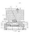
図2Aは、開示される実施形態による基板処理チャンバ1001である。遠隔プラズマシステム1010は、その後にガス入り口アセンブリ1011を通過する、フッ素含有前駆体を処理しうる。二つの別個のガス供給チャネルが、ガス入り口アセンブリ1011の中に見える。第一のチャネル1012が、遠隔プラズマシステム1010(RPS)を通過するガスを運び、一方、第二のチャネル1013は、遠隔プラズマシステム1010を迂回する。実施形態において、いずれのチャネルが、フッ素含有前駆体のために用いられてもよい。他方、第一のチャネル1012が、プロセスガスのために使用されてもよいし、第二のチャネル1013が、処理ガスのために使用されてもよい。リッド(又は導電性頂上部)1021及び貫通孔のあるパーティション1053が、その間にある絶縁リング1024とともに示され、このリングは、AC電位が、貫通孔のあるパーティション1053に対してリッド1021に印加されることを可能にする。AC電位が、チャンバプラズマ領域1020の中でプラズマを発生させる。プロセスガスは、第一のチャネル1012を通って、チャンバプラズマ領域1020の中へ進み、チャンバプラズマ領域1020の中のプラズマのみによって、又は遠隔プラズマシステム1010と組み合わされて、励起されうる。もしプロセスガス(フッ素含有前駆体)が、第二のチャネル1013を通って流れるならば、その場合、チャンバプラズマ領域1020のみが、励起のために使用される。チャンバプラズマ領域1020及び/又は遠隔プラズマシステム1010の結合は、本明細書中で、遠隔プラズマシステムと呼ばれうる。貫通孔のあるパーティション(シャワーヘッドとも呼ばれる)1053は、チャンバプラズマ領域1020を、シャワーヘッド1053の下の基板処理領域1070から分離する。シャワーヘッド1053は、チャンバプラズマ領域1020の中にあるプラズマが、基板処理領域1070の中のガスを直接に励起することを回避することを可能にするが、一方で、励起された種が、チャンバプラズマ領域1020から基板処理領域1070の中へ進むことを可能にする。 FIG. 2A is a
シャワーヘッド1053が、チャンバプラズマ領域1020と基板処理領域1070の間に配置され、そして、遠隔プラズマシステム1010及び/又はチャンバプラズマ領域1020の内部で作られるプラズマ流出物(前駆体の励起された誘導体又は他のガス)が、プレートの厚さを横切る複数の貫通孔1056を通過することを可能にする。シャワーヘッド1053はまた、蒸気又はガスの形の前駆体で充填されることができ、小さい孔1055を通って基板処理領域1070の中へ進むが、直接にチャンバプラズマ領域1020の中へ進まない、一つ又は複数の中空の容積1051を持つ。中空の容積1051はまた、特定のプロセスを達成するためにプラズマによる励起を必要としない前駆体のために使用されうる。シャワーヘッド1053は、この開示される実施形態において、貫通孔1056の最小直径1050の長さより厚い。チャンバプラズマ領域1020から基板処理領域1070へ通る励起された種のかなり大きい濃度を維持するために、貫通孔の最小直径1050の長さ226は、シャワーヘッド1053を貫いて途中まで貫通孔1056のより大きな直径部分を形成することにより、制限されうる。貫通孔1056の最小直径1050の長さは、開示される実施形態において、貫通孔1056の最小直径と同じ桁又はそれ未満でありうる。 A
シャワーヘッド1053は、図2Aに示されるように、イオンサプレッサの目的に役立つように、構成されうる。代替的には、基板処理領域1070の中に進むイオン濃度を抑制する別の処理チャンバ要素が、含まれうる(図示されていない)。リッド1021及びシャワーヘッド1053が、異なる電圧を受けるように、リッド1021及びシャワーヘッド1053は、それぞれ、第一の電極及び第二の電極として機能しうる。これらの構成において、電力(例えば、RF電力)が、リッド1021、シャワーヘッド1053又は両方に印加されうる。例えば、シャワーヘッド1053(イオンサプレッサとして働く)が接地される一方で、電力がリッド1021に印加されうる。基板処理システムは、リッド及び/又はシャワーヘッド1053に電力を供給するRFジェネレータを含みうる。リッド1021に印加される電圧は、チャンバプラズマ領域1020の中のプラズマの均一な分布を促進しうる(すなわち、局所プラズマを減少させうる)。チャンバプラズマ領域1020の中のプラズマの形成を可能にするために、絶縁リング1024が、リッド1021をシャワーヘッド1053から電気的に絶縁しうる。絶縁リング1024は、セラミックから作られうるし、スパークを回避するために、高い破壊電圧を持ちうる。上述した容量性結合プラズマ構成要素の近くの、基板処理チャンバ1001の部分は、プラズマに曝露される表面を、循環する冷却剤(例えば、水)で冷却するための、一つ又は複数の冷却流体チャネルを含む冷却ユニット(示されていない)を更に含みうる。 The
示された実施形態において、シャワーヘッド1053は、酸素、フッ素及び/若しくは窒素を含有するプロセスガス並びに/又はチャンバプラズマ領域1020の中でのプラズマによる励起による、そのようなプロセスガスのプラズマ流出物を(貫通孔1056を通じて)分配しうる。実施形態において、遠隔プラズマシステム1010の中へ及び/又はチャンバプラズマ領域1020の中へ導入されるプロセスガスは、フッ素を含有しうる(例えば、F2、NF3又はXeF2)。プロセスガスはまた、ヘリウム、アルゴン、窒素(N2)等などのキャリアガスを含みうる。プラズマ流出物は、プロセスガスのイオン化された又は中性の誘導体を含んでよく、導入されるプロセスガスの原子成分を指すラジカルフッ素前駆体とも、本明細書で呼ばれうる。In the illustrated embodiment, the
貫通孔1056は、チャンバプラズマ領域1020からのイオン帯電種の移動を抑制するが、他方、非帯電の中性又はラジカル種がシャワーヘッド1053を通って基板処理領域1070の中へと進むことを可能にするように、構成される。これらの非帯電種は、貫通孔1056によって反応性の低いキャリアガスとともに輸送される反応性の高い種を含みうる。上述のように、貫通孔1056によるイオン種の移動は、減少されうるし、場合によっては、完全に抑制されうる。シャワーヘッド1053を通過するイオン種の量を制御することは、下にあるウェハ基板と接触させられる混合ガスに対する制御を増大させ、これは次に、混合ガスの堆積及び/又はエッチング特性の制御を増大させる。例えば、混合ガスのイオン濃度の調整は、それのエッチング選択性(例えば、SiCx:SiOxエッチング比)を著しく変更することができる。The through-
実施形態において、貫通孔1056の数は、約60から約2000の間でありうる。貫通孔1056は、様々な形を持ちうるが、最も容易に、円形に作られる。貫通孔1056の最小直径1050は、開示される実施形態において、約0.5mmから約20mmの間、又は約1mmから約6mmの間でありうる。貫通孔の断面形状を選択するに際しても自由裁量があり、それは、円錐形、円柱形、又はその二つの形状の組合せに作られうる。基板処理領域1070の中に励起されていない前駆体を導入するために用いられる小さい孔1055の数は、異なる実施形態において、約100から約5000の間、又は約500から約2000の間でありうる。小さい孔1055の直径は、約0.1mmから約2mmの間でありうる。 In an embodiment, the number of through
貫通孔1056は、プラズマ活性ガス(すなわち、イオン、ラジカル及び/又は中性種)のシャワーヘッド1053の通過を制御するように、構成されうる。例えば、孔のアスペクト比(すなわち、孔の長さに対する直径)及び/又は孔の形状寸法は、シャワーヘッド1053を通る活性ガスの中のイオン帯電種の流量が減少するように、制御されうる。シャワーヘッド1053の中の貫通孔1056は、チャンバプラズマ領域1020に面するテーパ部、及び基板処理領域1070に面する円柱部を含みうる。円柱部は、基板処理領域1070の中へ進むイオン種の流量を制御するために、比例形成及び寸法形成されうる。調整可能な電気的バイアスもまた、シャワーヘッド1053を通るイオン種の流量を制御する追加手段として、シャワーヘッド1053に印加されうる。 The through-
代替的に、貫通孔1056は、シャワーヘッド1053の上面に向かって小さい内径(ID)を持ち、底面に向かって大きいIDを持ちうる。加えて、貫通孔1056の底部エッジは、プラズマ流出物がシャワーヘッドを出て行くときに、基板処理領域1070の中にプラズマ流出物を均等に分布させるのを助け、それによりプラズマ流出物及び前駆体ガスの均等な分布を促進するように、面取りされうる。小さいIDは、貫通孔1056に沿って様々な場所に置かれ、シャワーヘッド1053が基板処理領域1070の中のイオン密度を減少させることを、なお可能にしうる。イオン密度の減少は、基板処理領域1070の中に入る前の壁との衝突の数の増加に起因する。衝突の各々が、壁からの電子の獲得又は喪失によりイオンが中性化される確率を増加させる。概して、貫通孔1056の小さいIDは、約0.2mmから約20mmの間でありうる。他の実施形態において、小さいIDは、約1mmから6mmの間、又は約0.2mmから約5mmの間でありうる。更に、貫通孔1056のアスペクト比(すなわち、孔の長さに対する小さいID)は、およそ1から20でありうる。貫通孔の小さいIDは、貫通孔の長さに沿って見出される最小のIDでありうる。貫通孔1056の断面形状は、概して、円柱、円錐、又はそれの任意の組合せでありうる。 Alternatively, the through-
図2Bは、開示される実施形態による、処理チャンバとともに使用するためのシャワーヘッド1053の底面図である。シャワーヘッド1053は、図2Aに示されるシャワーヘッドに対応する。シャワーヘッド1053の底部に、大きい内径(ID)を有し、上部に小さいIDを有する貫通孔1056が、描かれている。小さい孔1055が、シャワーヘッドの表面上にわたって、貫通孔1056の間でさえ、実質的に均等に分布され、本明細書に記載される他の実施形態よりもより均等な混合を提供するのに役立つ。 FIG. 2B is a bottom view of a
フッ素含有プラズマ流出物及び酸素含有プラズマ流出物が、シャワーヘッド1053の中の貫通孔1056を通って到達するとき、例示的なパターン形成された基板が、基板処理領域1070の内部のペデスタル(示されていない)によって支持されうる。基板処理領域1070は、硬化などの他の処理のためにプラズマを維持するように装備されうるけれども、本発明の実施形態において、パターン形成された基板のエッチングの間、プラズマは存在しない。 When the fluorine-containing plasma effluent and the oxygen-containing plasma effluent reach through the through-
プラズマは、シャワーヘッド1053の上のチャンバプラズマ領域1020の中で、又はシャワーヘッド1053の下の基板処理領域1070の中で、発生されうる。フッ素含有前駆体の流入からラジカルフッ素前駆体を作るために、プラズマが、チャンバプラズマ領域1020の中に存在する。堆積の間にチャンバプラズマ領域の中にプラズマを発生させるために、通常は高周波(RF)域内にあるAC電圧が、処理チャンバの導電性頂上部(リッド1021)とシャワーヘッド1053の間に印加される。RF電源は、13.56MHzの高いRF周波数を発生させるが、単独で又は13.56MHz周波数と組合わせて、他の周波数をも発生させうる。 The plasma can be generated in the
基板処理領域1070の中の底部プラズマが、膜を硬化させるため又は基板処理領域1070を縁取る内部表面を洗浄するために生成されるとき、上部プラズマは、低電力又は電力なしにしておかれうる。シャワーヘッド1053とペデスタル又はチャンバの底部の間にAC電圧を印加することにより、基板処理領域1070の中のプラズマが、生成される。洗浄ガスが、プラズマが存在している間、基板処理領域1070の中に導入されうる。 When the bottom plasma in the
ペデスタルは、それを通って熱交換流体が基板の温度を制御するために流れる、熱交換チャネルを持ちうる。この構成は、基板温度が、比較的低い温度(室温から約120℃まで)を維持するように冷却又は加熱されることを可能にする。熱交換流体は、エチレングリコール及び水を含みうる。ペデスタルのウェハ支持体プラター(好ましくは、アルミニウム、セラミック、又はその組合せ)もまた、平行な同心円の形に2回転するように構成される埋め込まれた単一ループの埋め込まれたヒータ要素を用いて、比較的高い温度(約120℃から約1100℃まで)を達成するために、抵抗加熱されうる。ヒータ要素の内側部分が、より小さい半径を持つ同心円の軌道上を走る一方で、ヒータ要素の外側部分は、支持体プラターの周囲に隣接して走りうる。ヒータ要素への配線は、ペデスタルのステムを通る。 The pedestal can have a heat exchange channel through which heat exchange fluid flows to control the temperature of the substrate. This configuration allows the substrate temperature to be cooled or heated to maintain a relatively low temperature (from room temperature to about 120 ° C.). The heat exchange fluid may include ethylene glycol and water. A pedestal wafer support platter (preferably aluminum, ceramic, or a combination thereof) is also used with an embedded single loop embedded heater element that is configured to rotate twice in a parallel concentric shape. In order to achieve a relatively high temperature (from about 120 ° C. to about 1100 ° C.), it can be resistively heated. The inner portion of the heater element may run on a concentric orbit with a smaller radius, while the outer portion of the heater element may run adjacent to the periphery of the support platter. The wiring to the heater element passes through the pedestal stem.
基板処理システムは、システムコントローラによって制御される。代表的な実施形態において、システムコントローラは、ハードディスクドライブ、フロッピーディスクドライブ及びプロセッサを含む。プロセッサは、シングルボードコンピュータ(SBC)、アナログ及びデジタル入力/出力ボード、インターフェースボード及びステッパモータコントローラボードを含む。CVDシステムの種々の部品は、ボード、カードケージ、及びコネクタの寸法及び型を定義するVersa Modular European (VME)規格に従う。VME規格はまた、バス構造を、16ビットデータバス及び24ビットアドレスバスを持つと定義する。 The substrate processing system is controlled by a system controller. In an exemplary embodiment, the system controller includes a hard disk drive, a floppy disk drive, and a processor. The processor includes a single board computer (SBC), analog and digital input / output boards, interface boards and stepper motor controller boards. The various parts of the CVD system follow the Versa Modular European (VME) standard that defines board, card cage, and connector dimensions and types. The VME standard also defines the bus structure as having a 16-bit data bus and a 24-bit address bus.
システムコントローラは、エッチングチャンバの活動の全てを制御する。システムコントローラは、コンピュータ可読媒体の中に格納されるコンピュータプログラムである、システム制御ソフトウェアを実行する。好ましくは、媒体は、ハードディスクドライブであるが、媒体は、他の種類の記憶装置であってもよい。コンピュータプログラムは、特定のプロセスの、タイミング、ガスの混合、チャンバ圧力、チャンバ温度、RF電力レベル、サセプタ位置、及び他のパラメータを指示する命令のセットを含む。例えば、フロッピーディスク又は他の適当なドライバを含む、他の記憶装置上に格納された他のコンピュータプログラムが、システムコントローラに指示するために用いられてもよい。 The system controller controls all of the etching chamber activities. The system controller executes system control software, which is a computer program stored in a computer readable medium. Preferably, the medium is a hard disk drive, but the medium may be other types of storage devices. The computer program includes a set of instructions that indicate the timing, gas mixing, chamber pressure, chamber temperature, RF power level, susceptor position, and other parameters of a particular process. For example, other computer programs stored on other storage devices, including floppy disks or other suitable drivers, may be used to direct the system controller.
基板上に膜スタックを堆積させるためのプロセス又はチャンバを洗浄するためのプロセスが、システムコントローラにより実行されるコンピュータプログラム製品を用いて実行されうる。コンピュータプログラムコードは、任意の伝統的なコンピュータ可読プログラミング言語、例えば、68000アセンブリ言語、C、C++、Pascal、Fortran、又はその他で書くことができる。適当なプログラムコードが、通常のテキストエディタを用いて、単一のファイル又は複数のファイルの中に入れられ、そして、コンピュータのメモリシステムなどの、コンピュータ使用可能媒体の中に格納又は取り入れられる。入れられたコードテキストが、高級言語である場合、コードはコンパイルされ、結果として生じるコンパイラコードが、その後、プリコンパイルされたMicrosoft Windows(登録商標)ライブラリルーチンのオブジェクトコードとリンクされる。リンクされ、コンパイルされたオブジェクトコードを実行するために、システムのユーザは、オブジェクトコードを呼び出し、コンピュータシステムが、コードをメモリの中にロードするようにさせる。CPUは、それから、コードを読み、実行し、プログラムの中に同定されたタスクを実行する。 A process for depositing a film stack on a substrate or a process for cleaning a chamber may be performed using a computer program product executed by a system controller. The computer program code can be written in any traditional computer readable programming language, eg, 68000 assembly language, C, C ++, Pascal, Fortran, or others. Appropriate program code is placed in a single file or multiple files using a conventional text editor and stored or incorporated in a computer-usable medium, such as a computer memory system. If the entered code text is a high-level language, the code is compiled and the resulting compiler code is then linked with the precompiled Microsoft Windows library object code. To execute the linked and compiled object code, the user of the system calls the object code and causes the computer system to load the code into memory. The CPU then reads and executes the code and performs the tasks identified in the program.
ユーザとコントローラとの間のインターフェースは、フラットパネルタッチセンスモニタを含みうる。好適な実施形態において、二つのモニタが用いられ、一つはオペレータのためにクリーンルームの壁の中に据え付けられ、もう一つはサービス技術者のために壁の後ろに据え付けられる。二つのモニタが、同じ情報を同時に表示してもよく、その場合、一度に一つだけが、入力を受け取る。特定のスクリーン又は機能を選択するために、オペレータは、タッチセンスモニタの指定された領域をタッチする。タッチされた領域は、ハイライト表示された色を変化させ、又は新しいメニュー若しくはスクリーンが表示され、オペレータとタッチセンスモニタの間のコミュニケーションを確認する。キーボード、マウス、又は他のポインティング若しくはコミュニケーション装置などの他の装置が、ユーザがシステムコントローラと通信することを可能にするために、タッチセンスモニタの代わりに又はそれに加えて使用されうる。 The interface between the user and the controller may include a flat panel touch sense monitor. In a preferred embodiment, two monitors are used, one installed in the clean room wall for the operator and the other installed behind the wall for the service technician. Two monitors may display the same information simultaneously, in which case only one at a time receives input. To select a particular screen or function, the operator touches a designated area of the touch sensitive monitor. The touched area changes the highlighted color or a new menu or screen is displayed to confirm communication between the operator and the touch sensitive monitor. Other devices such as a keyboard, mouse, or other pointing or communication device can be used in place of or in addition to the touch-sensitive monitor to allow the user to communicate with the system controller.
チャンバプラズマ領域又は遠隔プラズマシステムの中の領域は、遠隔プラズマ領域と呼ばれうる。実施形態において、ラジカル前駆体(例えば、ラジカルフッ素前駆体及びラジカル酸素前駆体)が、遠隔プラズマ領域の中に形成され、基板処理領域の中に進み、そこで、その結合は、ケイ素‐窒素‐及び炭素含有材料を優先的にエッチングする。ラジカルフッ素前駆体及びラジカル酸素前駆体が、基板処理領域の中で更に励起されないことを保証するため、実施形態において、プラズマ出力は、遠隔プラズマ領域に対してのみ、本質的に印加されうる。 A region in the chamber plasma region or remote plasma system may be referred to as a remote plasma region. In embodiments, radical precursors (eg, radical fluorine precursors and radical oxygen precursors) are formed in the remote plasma region and proceed into the substrate processing region, where the bonds are silicon-nitrogen-and The carbon-containing material is preferentially etched. In an embodiment, the plasma power can be essentially applied only to the remote plasma region to ensure that the radical fluorine precursor and radical oxygen precursor are not further excited in the substrate processing region.
チャンバプラズマ領域を用いる実施形態において、励起されたプラズマ流出物が、堆積領域から仕切られた基板処理領域のセクションの中で生成される。本明細書中で基板処理領域としても知られる堆積領域は、パターン形成された基板(例えば、半導体ウェハ)をエッチングするために、プラズマ流出物が、混合し反応するところである。励起されたプラズマ流出物はまた、不活性ガス(例示的な場合において、アルゴン)により、伴われうる。基板処理領域は、パターン形成された基板のエッチングの間、「プラズマフリー」と、本明細書中で記載されうる。「プラズマフリー」は、領域にプラズマがないということを、必ずしも意味しない。プラズマ領域の中で作られる比較的低い濃度のイオン化種及び自由電子が、貫通孔1056の形及び大きさのため、パーティション(シャワーヘッド/イオンサプレッサ)の中の孔(開孔)を通って進む。いくつかの実施形態において、偏在する意図されない放射の回避できない源を除いて、基板処理領域の中に、いかなる濃度のイオン化種及び自由電子も存在しない。チャンバプラズマ領域の中のプラズマの境界は、定義することが難しく、シャワーヘッドの中の開孔を通って基板処理領域に侵入しうる。誘導結合プラズマの場合、基板処理領域の中で直接に、少量のイオン化が行われうる。更に、低強度のプラズマが、形成している膜の望ましい特徴を除去することなく、基板処理領域の中で作られうる。励起されたプラズマ流出物の生成の間、チャンバプラズマ領域(又は、その点において、遠隔プラズマ領域)よりもはるかに低い強度のイオン密度を持つプラズマに対する全ての原因が、本明細書で用いられる「プラズマフリー」の範囲から逸脱しない。 In embodiments using a chamber plasma region, an excited plasma effluent is generated in a section of the substrate processing region that is partitioned from the deposition region. A deposition region, also known herein as a substrate processing region, is where the plasma effluent mixes and reacts to etch a patterned substrate (eg, a semiconductor wafer). The excited plasma effluent can also be accompanied by an inert gas (argon in the exemplary case). The substrate processing region may be described herein as “plasma free” during the etching of the patterned substrate. “Plasma-free” does not necessarily mean that there is no plasma in the region. Due to the shape and size of the through-
三フッ化窒素(又は他のフッ素含有前駆体)が、異なる実施形態において、約25sccmから約200sccmの間、約50sccmから約150sccmの間、又は約75sccmから約125sccmの間の速度で、チャンバプラズマ領域1020の中に流されうる。酸素(O2)が、異なる実施形態において、約25sccmから約200sccmの間、約50sccmから約150sccmの間、又は約75sccmから約125sccmの間の速度で、チャンバプラズマ領域1020の中に流されうる。Nitrogen trifluoride (or other fluorine-containing precursor) is at a rate of between about 25 sccm and about 200 sccm, between about 50 sccm and about 150 sccm, or between about 75 sccm and about 125 sccm in different embodiments. Can be flushed into
チャンバの中へのフッ素含有前駆体及び酸素含有前駆体の結合された流量が、体積で混合ガス全部の0.05%から約20%を占めうる。残りはキャリアガスである。実施形態において、フッ素含有前駆体及び酸素含有前駆体が、遠隔プラズマ領域の中に流されるが、プラズマ流出物は、同じ体積測定の流量比を持つ。フッ素含有前駆体の場合、遠隔プラズマ領域の中の圧力を安定化させるために、パージ又はキャリアガスが、フッ素含有ガスの前に、遠隔プラズマ領域の中に最初に入れられうる。 The combined flow rate of fluorine-containing precursor and oxygen-containing precursor into the chamber can account for 0.05% to about 20% of the total gas mixture by volume. The rest is carrier gas. In an embodiment, a fluorine-containing precursor and an oxygen-containing precursor are flowed into the remote plasma region, but the plasma effluent has the same volumetric flow ratio. In the case of a fluorine-containing precursor, a purge or carrier gas can be initially placed in the remote plasma region prior to the fluorine-containing gas to stabilize the pressure in the remote plasma region.
プラズマ出力は、種々の周波数又は複数の周波数の組合せでありうる。例示的な処理システムにおいて、プラズマは、リッド1021とシャワーヘッド1053の間に供給されるRF電力により供給される。RF電力は、異なる実施形態において、約10ワットから約2000ワットの間、約20ワットから約1500ワットの間、又は約50ワットから約500ワットの間でありうる。例示的な処理システムの中で印加されるRF周波数は、異なる実施形態において、約200kHzより低い低RF周波数、約10MHzと約15MHzの間の高RF周波数、又は1GHzより大きい若しくは約1GHzのマイクロ波周波数でありうる。 The plasma power can be various frequencies or a combination of frequencies. In the exemplary processing system, the plasma is supplied by RF power supplied between the
基板処理領域1070の中へのキャリアガス及びプラズマ流出物の流入の間、基板処理領域1070は、種々の圧力に維持されることができる。基板処理領域内の圧力は、50トル未満若しくは約50トル、30トル未満若しくは約30トル、20トル未満若しくは約20トル、10トル未満若しくは約10トル、又は5トル未満若しくは約5トルである。圧力は、本発明の実施形態において、0.1トルより高い若しくは約0、1トル、0.2トルより高い若しくは約0、2トル、0.5トルより高い若しくは0.5トル、又は1トルより高い若しくは約1トルでありうる。本発明の更なる実施形態に到達するために、圧力の下限は、圧力の上限と組み合わされうる。 During the inflow of carrier gas and plasma effluent into the
一つ又は複数の実施形態において、基板処理チャンバ1001は、Santa Clara、Calif.に所在するApplied Materials,Inc.から入手可能な、Producer(商標)GT、Centura(商標)AP及びEndura(商標)プラットフォームを含む、種々のマルチ処理プラットフォームの中に統合されることができる。そのような処理プラットフォームは、真空を破壊することなく、幾つかの処理作業を行なうことができる。本発明の実施形態を実行しうる処理チャンバは、数ある種類のチャンバの中で、誘電体エッチングチャンバ又は種々の化学気相堆積チャンバを含みうる。 In one or more embodiments, the
堆積システムの実施形態は、集積回路チップを生産するためのより大きな製造システムの中に組込まれうる。図3は、開示される実施形態による、堆積、エッチング、焼成及び硬化チャンバの一つのそのようなシステム1101を示す。図において、1対のFOUP(前方開口型統一ポッド)1102が、基板(例えば、300mm直径ウェハ)を供給し、基板は、ロボットアーム1104によって受け取られ、低圧ホールドエリア1106の中に置かれ、ウェハ処理チャンバ1108a‐fのうちの一つの中に置かれる。第二のロボットアーム1110が、低圧ホールドエリア1106からウェハ処理チャンバ1108a‐fへ、及びその逆方向に、基板ウェハを輸送するために用いられうる。各ウェハ処理チャンバ1108a‐fが、周期的層堆積(CLD)、原子層堆積(ALD)、化学気相堆積(CVD)、物理気相堆積(PVD)、エッチング、前洗浄、ガス抜き、配向、及び他の基板処理に加えて、本明細書に記載されるドライエッチング処理を含む、幾つかの基板処理作業を行うように、装備されることができる。 Embodiments of the deposition system can be incorporated into a larger manufacturing system for producing integrated circuit chips. FIG. 3 shows one such system 1101 of a deposition, etch, bake and cure chamber according to disclosed embodiments. In the figure, a pair of FOUPs (front opening unified pods) 1102 supply a substrate (eg, a 300 mm diameter wafer), which is received by a
ウェハ処理チャンバ1108a‐fは、基板ウェハ上で流動可能な誘電体膜を堆積し、アニールし、硬化し、及び/又はエッチングするための一つ又は複数のシステム構成要素を含みうる。一つの構成において、2対の処理チャンバ(例えば、1108c‐d及び1108e‐f)が、誘電体材料を基板上に堆積するために使用されうるし、そして、第三の対の処理チャンバ(例えば、1108a‐b)が、堆積された誘電体をエッチングするために使用されうる。別の構成において、3対全てのチャンバ(例えば、1108a‐f)が、基板上の誘電体膜をエッチングするように構成されうる。記載されたプロセスの任意の一つ又は複数が、種々の実施形態に示される製造システムから分離されたチャンバ(複数可)上で実行されうる。
システムコントローラ1157が、モータ、バルブ、流量コントローラ、電源、及び本明細書に記載されるプロセスレシピを実行するために必要とされる他の機能を制御するために使用される。ガスハンドリングシステム1155もまた、ウェハ処理チャンバ1108a‐fのうちの一つ又は全てにガスを導入するために、システムコントローラ1157により制御されうる。システムコントローラ1157は、ガスハンドリングシステム1155の中の及び/又はウェハ処理チャンバ1108a‐fの中の移動可能な機械的アセンブリの位置を決定し調整するために、光センサからのフィードバックに依存しうる。機械的アセンブリは、システムコントローラ1157の制御の下でモータにより移動されるロボット、スロットルバルブ及びサセプタを含みうる。 A
代表的な実施形態において、システムコントローラ1157は、ハードディスクドライブ(メモリ)、USBポート、フロッピーディスクドライブ及びプロセッサを含む。システムコントローラ1157は、アナログ及びデジタル入力/出力ボード、インターフェースボード及びステッパモータコントローラボードを含む。基板処理チャンバ1001を含むマルチチャンバ処理システム1101の様々な部分が、システムコントローラ1157により制御される。システムコントローラは、ハードディスク、フロッピーディスク又はフラッシュメモリサムドライブなどのコンピュータ可読媒体上に格納されたコンピュータプログラムの形のシステム制御ソフトウェアを実行する。他の種類の記憶装置が使用されることもできる。コンピュータプログラムは、特定のプロセスの、タイミング、ガスの混合、チャンバ圧力、チャンバ温度、RF電力レベル、サセプタ位置、及び他のパラメータを指示する命令のセットを含む。 In an exemplary embodiment, the
基板上で膜をエッチングする、堆積させる若しくは他の方法で処理するためのプロセス、又はチャンバを洗浄するためのプロセスが、コントローラにより実行されるコンピュータプログラム製品を用いて実行されうる。コンピュータプログラムコードは、任意の伝統的なコンピュータ可読プログラミング言語、例えば、68000アセンブリ言語、C、C++、Pascal, Fortran、又はその他で書くことができる。適当なプログラムコードが、通常のテキストエディタを用いて、単一のファイル又は複数のファイルの中に入れられ、そして、コンピュータのメモリシステムなどの、コンピュータ使用可能媒体の中に格納又は取り入れられる。入れられたコードテキストが、高級言語である場合、コードはコンパイルされ、結果として生じるコンパイラコードが、その後、プリコンパイルされたMicrosoft Windows(登録商標)ライブラリルーチンのオブジェクトコードとリンクされる。リンクされ、コンパイルされたオブジェクトコードを実行するために、システムのユーザは、オブジェクトコードを呼び出し、コンピュータシステムが、コードをメモリの中にロードするようにさせる。CPUは、それから、コードを読み、実行し、プログラムの中に同定されたタスクを行なう。 A process for etching, depositing or otherwise processing a film on a substrate, or a process for cleaning a chamber may be performed using a computer program product executed by a controller. The computer program code can be written in any traditional computer readable programming language, such as 68000 assembly language, C, C ++, Pascal, Fortran, or others. Appropriate program code is placed in a single file or multiple files using a conventional text editor and stored or incorporated in a computer-usable medium, such as a computer memory system. If the entered code text is a high-level language, the code is compiled and the resulting compiler code is then linked with the precompiled Microsoft Windows library object code. To execute the linked and compiled object code, the user of the system calls the object code and causes the computer system to load the code into memory. The CPU then reads and executes the code and performs the tasks identified in the program.
ユーザとコントローラの間のインターフェースは、タッチセンスモニタによってもよく、マウス及びキーボードをも含みうる。一つの実施形態において、二つのモニタが用いられ、一つはオペレータのためにクリーンルームの壁の中に据え付けられ、もう一つはサービス技術者のために壁の後ろに据え付けられる。二つのモニタが、同じ情報を同時に表示してもよく、その場合、一度に一つだけが、入力を受け取るように構成される。特定のスクリーン又は機能を選択するために、オペレータは、表示スクリーン上の指定された領域を、指又はマウスでタッチする。タッチされた領域は、ハイライト表示された色を変化させ、又は新しいメニュー若しくはスクリーンが表示され、オペレータの選択を確認する。 The interface between the user and the controller may be a touch sensitive monitor and may also include a mouse and keyboard. In one embodiment, two monitors are used, one installed in the clean room wall for the operator and the other installed behind the wall for the service technician. Two monitors may display the same information simultaneously, in which case only one is configured to receive input at a time. To select a particular screen or function, the operator touches a designated area on the display screen with a finger or mouse. The touched area changes the highlighted color or a new menu or screen is displayed to confirm the operator's selection.
本明細書で使用されるとき、「基板」は、その上に形成される層を有する又は有しない支持体基板でありうる。パターン形成された基板は、種々のドーピング濃度及びプロファイルの絶縁体又は半導体であってよく、例えば、集積回路の製造で使用される種類の半導体基板でありうる。パターン形成された基板の露出された「酸化ケイ素」は、主にSiO2であるが、窒素、水素、炭素などの他の元素成分の濃度を含んでよい。幾つかの実施形態において、本明細書に開示される方法を用いてエッチングされる酸化ケイ素膜は、本質的にケイ素及び酸素からなる。「前駆体」という用語は、材料を表面から除去するか又は材料を表面上に堆積させるための反応に関与する任意のプロセスガスを指すために用いられる。「プラズマ流出物」は、チャンバプラズマ領域から出て、基板処理領域に入るガスを言う。プラズマ流出物は、ガス分子の少なくとも一部が、振動励起状態、解離状態及び/又はイオン化状態である「励起状態」にある。「ラジカル前駆体」は、材料を表面から除去するか又は材料を表面上に堆積させるための反応に関与するプラズマ流出物(プラズマを終了しつつある励起状態にあるガス)を記述するために用いられる。「ラジカル酸素前駆体」は、酸素を含有するが、他の元素成分を含有しうるラジカル前駆体である。「ラジカルフッ素前駆体」は、フッ素を含有するが、他の元素成分を含有しうるラジカル前駆体である。「ラジカル酸素前駆体」及び「ラジカルフッ素前駆体」は、それぞれ、「酸素含有プラズマ流出物」及び「フッ素含有プラズマ流出物」と同等である。「不活性ガス」という語句は、膜をエッチングするとき又は膜の中に組み入れられるときに、化学結合を形成しない任意のガスを指す。代表的な不活性ガスは、希ガスを含むが、(典型的には)痕跡量が膜の中に捕えられるときに、いかなる化学結合も形成されない限り、他のガスを含んでよい。As used herein, a “substrate” can be a support substrate with or without a layer formed thereon. The patterned substrate may be an insulator or semiconductor of various doping concentrations and profiles, for example, a type of semiconductor substrate used in the manufacture of integrated circuits. The exposed “silicon oxide” of the patterned substrate is primarily SiO2 , but may include concentrations of other elemental components such as nitrogen, hydrogen, and carbon. In some embodiments, the silicon oxide film etched using the methods disclosed herein consists essentially of silicon and oxygen. The term “precursor” is used to refer to any process gas that participates in a reaction to remove material from or deposit material on a surface. “Plasma effluent” refers to a gas that exits the chamber plasma region and enters the substrate processing region. The plasma effluent is in an “excited state” in which at least some of the gas molecules are in a vibrationally excited state, a dissociated state and / or an ionized state. “Radical precursor” is used to describe the plasma effluent (the excited gas that is terminating the plasma) that is involved in the reaction to remove the material from the surface or to deposit the material on the surface. It is done. A “radical oxygen precursor” is a radical precursor that contains oxygen but may contain other elemental components. A “radical fluorine precursor” is a radical precursor that contains fluorine but may contain other elemental components. “Radical oxygen precursor” and “radical fluorine precursor” are equivalent to “oxygen-containing plasma effluent” and “fluorine-containing plasma effluent”, respectively. The phrase “inert gas” refers to any gas that does not form a chemical bond when the film is etched or incorporated into the film. Typical inert gases include noble gases, but (typically) other gases may be included so long as no chemical bonds are formed when trace amounts are trapped in the membrane.
「間隙」及び「トレンチ」という用語は、エッチングされる形状寸法が大きな水平アスペクト比を持つということを含意せず、終始用いられる。表面上から見ると、トレンチは、円形、長円形、多角形、長方形、又は種々の他の形に見えうる。トレンチは、材料の島の周囲の堀の形でありうる。「ビア」という用語は、垂直の電気的接続を形成するために、金属で充填されていてもよいし又はされていなくてもよい低アスペクト比トレンチ(上から見て)を指すために、用いられる。本明細書で使用されるとき、共形エッチングプロセスとは、表面と同じ形状での、表面上の材料の概して均一な除去を指し、すなわち、エッチングされた層の表面とエッチング前の表面とが概して平行である。当業者は、エッチングされるインターフェースが100%共形ということはありそうにないということを認めるであろうから、「概して」という用語は、受入可能な許容範囲を見込む。 The terms “gap” and “trench” are used throughout, without implying that the etched geometry has a large horizontal aspect ratio. Viewed from above, the trenches can appear circular, oval, polygonal, rectangular, or various other shapes. The trench can be in the form of a moat around an island of material. The term “via” is used to refer to a low aspect ratio trench (viewed from above) that may or may not be filled with metal to form a vertical electrical connection. It is done. As used herein, a conformal etching process refers to a generally uniform removal of material on a surface in the same shape as the surface, i.e., the surface of the etched layer and the surface prior to etching. They are generally parallel. Those skilled in the art will appreciate that the interface being etched is unlikely to be 100% conformal, so the term “generally” allows for acceptable tolerances.
幾つかの実施形態を開示してきたが、様々な修正、代替的な構成、及び同等物が、開示される実施形態の精神から逸脱することなく、用いられうるということが、当業者により認められるであろう。加えて、本発明を不必要に不明瞭にすることを回避するために、幾つかの既知のプロセス及び要素が、記載されなかった。従って、上記記載は、本発明の範囲を限定するとみなされるべきではない。 While several embodiments have been disclosed, those skilled in the art will recognize that various modifications, alternative configurations, and equivalents may be used without departing from the spirit of the disclosed embodiments. Will. In addition, some known processes and elements have not been described in order to avoid unnecessarily obscuring the present invention. Therefore, the above description should not be taken as limiting the scope of the invention.
数値の範囲が与えられる場合、その範囲の上限と下限の間に入る各数値もまた、明らかに文脈が異なって要求しない限り、下限の単位の10分の1まで、明確に開示されるということが、理解される。述べられた範囲の中の任意の述べられた数値又は間に入っている数値と、その述べられた範囲の中の任意の他の述べられた数値又は間に入っている数値との間の、小さい範囲の各々が、包含される。これらの小さい範囲の上限及び下限は、独立に、その範囲の中に含まれてもよいし、又は除外されてもよく、そして、上限及び下限のいずれか又は両方が小さい範囲に含まれる、又はいずれも含まれないような範囲の各々もまた、述べられた範囲の中の明確に除外される上限又は下限を前提として、本発明の中に包含される。所定の範囲が、上限及び下限の一つ又は両方を含む場合、それら含まれる上限及び下限のいずれか又は両方を除外する範囲もまた含まれる。 When a range of numbers is given, each number that falls between the upper and lower limits of the range is also clearly disclosed, up to one-tenth of the lower limit unit, unless clearly stated otherwise in context. Is understood. Between any stated numerical value or intervening numerical value within the stated range and any other stated numerical value or intervening numerical value within the stated range; Each small range is included. The upper and lower limits of these small ranges may independently be included in or excluded from the range, and either or both of the upper and lower limits are included in the small range, or Each such range that is not included is also included in the present invention, subject to the upper or lower limit explicitly excluded from the stated range. Where a given range includes one or both of an upper limit and a lower limit, ranges excluding either or both of the included upper and lower limits are also included.
本明細書及び添付の特許請求の範囲において用いられる場合、単数形「一つの(a)」、「一つの(an)」、及び「その(the)」は、明らかに文脈が異なった要求をしていない限り、複数の参照対象を含む。したがって、例えば、「一つのプロセス(a process)」への言及は、複数のそのようなプロセスを含み、「その誘電体材料(the dielectric material)」への言及は、一つ又は複数の誘電体材料及び当業者に既知のその同等物への言及を含む、等々である。 As used in this specification and the appended claims, the singular forms “a”, “an”, and “the” refer to clearly different contextual requirements. Unless otherwise specified, includes multiple references. Thus, for example, reference to “a process” includes a plurality of such processes, and a reference to “the dielectric material” includes one or more dielectrics Including references to materials and equivalents known to those skilled in the art, and so on.
また、「含む(comprise)」、「含んでいる(comprising)」、「含む(include)」、「含んでいる(including)」及び「含む(includes)」という言葉は、本明細書及び以下の特許請求の範囲において用いられる場合、述べられた特徴、整数、構成要素又はステップの存在を明示するように意図されるが、一つ又は複数の他の特徴、整数、構成要素、ステップ、行為又はグループの存在又は追加を排除しない。 Also, the terms “comprise”, “comprising”, “include”, “including” and “includes” are used herein and in the following. When used in the claims, it is intended to clarify the existence of the stated feature, integer, component or step, but one or more other features, integers, components, steps, acts or Does not exclude the presence or addition of groups.
Claims (20)
Translated fromJapaneseプラズマ流出物を作るために遠隔プラズマ領域の中でプラズマを形成している間、前記基板処理領域と流体結合した前記遠隔プラズマ領域の中にフッ素含有前駆体及び酸素含有前駆体の各々を流す流し工程であって、前記遠隔プラズマ領域の中にフッ素含有前駆体及び酸素含有前駆体の各々を流す際に、O:Fの原子流量比が約2:1ないし2:1を超える値に、または約10:1ないし10:1を超えない値に保たれる流し工程、及び
シャワーヘッドの中の貫通孔を通して前記プラズマ流出物を前記基板処理領域の中に流すことにより、前記露出されたケイ素‐窒素‐炭素含有領域をエッチングするエッチング工程であって、前記プラズマ流出物は水素を欠いており、エッチングの選択性は露出された酸化シリコン域に対する前記露出されたケイ素‐窒素‐炭素含有領域のエッチング速度比で定められるものであって、前記エッチングの選択性は、約150または150を超えるエッチング工程を含む、方法。Exposed silicon - nitrogen - carbon containing region, and theexposed silicon oxide (SiO2) pattern shapeSeiki platehaving a frequency, a method of etching in the substrate processing region of a substrate processingchamber,
A flow forflowing each of the fluorine-containing precursor and the oxygen-containing precursor into the remote plasma region fluidly coupled to the substrate processing region while forming a plasma in the remote plasma region to create a plasma effluent.A flow rate of O: F of about 2: 1 to greater than 2: 1 when each of the fluorine-containing precursor and the oxygen-containing precursor is flowed into the remote plasma region, or A flow step maintained at a value not exceeding about 10: 1 to no greater than 10: 1 , andflowing the plasma effluent into the substrate processing region through a through-hole in a showerhead, thereby exposing the exposed silicon nitrogen-a etching step of etching thecarbon-containingregion, the plasma effluent lacks a hydrogen, the etching selectivity is the exposure to a silicon oxide zone, which is exposed And a etch rate ratio of the silicon-nitrogen-carbon containing region, wherein the etch selectivity comprises about 150 or more than 150 etching steps .
Applications Claiming Priority (5)
| Application Number | Priority Date | Filing Date | Title |
|---|---|---|---|
| US201261703612P | 2012-09-20 | 2012-09-20 | |
| US61/703,612 | 2012-09-20 | ||
| US13/833,033US9390937B2 (en) | 2012-09-20 | 2013-03-15 | Silicon-carbon-nitride selective etch |
| US13/833,033 | 2013-03-15 | ||
| PCT/US2013/057253WO2014046858A1 (en) | 2012-09-20 | 2013-08-29 | Silicon-carbon-nitride selective etch |
Publications (2)
| Publication Number | Publication Date |
|---|---|
| JP2015529405A JP2015529405A (en) | 2015-10-05 |
| JP6272873B2true JP6272873B2 (en) | 2018-01-31 |
Family
ID=50274905
Family Applications (1)
| Application Number | Title | Priority Date | Filing Date |
|---|---|---|---|
| JP2015533083AExpired - Fee RelatedJP6272873B2 (en) | 2012-09-20 | 2013-08-29 | Selective etching of silicon carbonitride |
Country Status (6)
| Country | Link |
|---|---|
| US (1) | US9390937B2 (en) |
| JP (1) | JP6272873B2 (en) |
| KR (1) | KR102159750B1 (en) |
| CN (1) | CN104838479B (en) |
| TW (1) | TWI618139B (en) |
| WO (1) | WO2014046858A1 (en) |
Families Citing this family (139)
| Publication number | Priority date | Publication date | Assignee | Title |
|---|---|---|---|---|
| US9324576B2 (en) | 2010-05-27 | 2016-04-26 | Applied Materials, Inc. | Selective etch for silicon films |
| US10283321B2 (en) | 2011-01-18 | 2019-05-07 | Applied Materials, Inc. | Semiconductor processing system and methods using capacitively coupled plasma |
| US9064815B2 (en) | 2011-03-14 | 2015-06-23 | Applied Materials, Inc. | Methods for etch of metal and metal-oxide films |
| US8999856B2 (en) | 2011-03-14 | 2015-04-07 | Applied Materials, Inc. | Methods for etch of sin films |
| US8808563B2 (en) | 2011-10-07 | 2014-08-19 | Applied Materials, Inc. | Selective etch of silicon by way of metastable hydrogen termination |
| US9267739B2 (en) | 2012-07-18 | 2016-02-23 | Applied Materials, Inc. | Pedestal with multi-zone temperature control and multiple purge capabilities |
| US9373517B2 (en) | 2012-08-02 | 2016-06-21 | Applied Materials, Inc. | Semiconductor processing with DC assisted RF power for improved control |
| US9034770B2 (en) | 2012-09-17 | 2015-05-19 | Applied Materials, Inc. | Differential silicon oxide etch |
| US9023734B2 (en) | 2012-09-18 | 2015-05-05 | Applied Materials, Inc. | Radical-component oxide etch |
| US9132436B2 (en) | 2012-09-21 | 2015-09-15 | Applied Materials, Inc. | Chemical control features in wafer process equipment |
| US8969212B2 (en) | 2012-11-20 | 2015-03-03 | Applied Materials, Inc. | Dry-etch selectivity |
| US8980763B2 (en) | 2012-11-30 | 2015-03-17 | Applied Materials, Inc. | Dry-etch for selective tungsten removal |
| US9111877B2 (en) | 2012-12-18 | 2015-08-18 | Applied Materials, Inc. | Non-local plasma oxide etch |
| US8921234B2 (en) | 2012-12-21 | 2014-12-30 | Applied Materials, Inc. | Selective titanium nitride etching |
| US10256079B2 (en) | 2013-02-08 | 2019-04-09 | Applied Materials, Inc. | Semiconductor processing systems having multiple plasma configurations |
| US9362130B2 (en) | 2013-03-01 | 2016-06-07 | Applied Materials, Inc. | Enhanced etching processes using remote plasma sources |
| US9040422B2 (en) | 2013-03-05 | 2015-05-26 | Applied Materials, Inc. | Selective titanium nitride removal |
| US20140271097A1 (en) | 2013-03-15 | 2014-09-18 | Applied Materials, Inc. | Processing systems and methods for halide scavenging |
| US9493879B2 (en) | 2013-07-12 | 2016-11-15 | Applied Materials, Inc. | Selective sputtering for pattern transfer |
| US9773648B2 (en) | 2013-08-30 | 2017-09-26 | Applied Materials, Inc. | Dual discharge modes operation for remote plasma |
| US9576809B2 (en) | 2013-11-04 | 2017-02-21 | Applied Materials, Inc. | Etch suppression with germanium |
| US9520303B2 (en) | 2013-11-12 | 2016-12-13 | Applied Materials, Inc. | Aluminum selective etch |
| US9245762B2 (en) | 2013-12-02 | 2016-01-26 | Applied Materials, Inc. | Procedure for etch rate consistency |
| US9287095B2 (en) | 2013-12-17 | 2016-03-15 | Applied Materials, Inc. | Semiconductor system assemblies and methods of operation |
| US9287134B2 (en) | 2014-01-17 | 2016-03-15 | Applied Materials, Inc. | Titanium oxide etch |
| US9293568B2 (en) | 2014-01-27 | 2016-03-22 | Applied Materials, Inc. | Method of fin patterning |
| US9396989B2 (en) | 2014-01-27 | 2016-07-19 | Applied Materials, Inc. | Air gaps between copper lines |
| US9385028B2 (en) | 2014-02-03 | 2016-07-05 | Applied Materials, Inc. | Air gap process |
| US9499898B2 (en) | 2014-03-03 | 2016-11-22 | Applied Materials, Inc. | Layered thin film heater and method of fabrication |
| US9299575B2 (en) | 2014-03-17 | 2016-03-29 | Applied Materials, Inc. | Gas-phase tungsten etch |
| US9299537B2 (en) | 2014-03-20 | 2016-03-29 | Applied Materials, Inc. | Radial waveguide systems and methods for post-match control of microwaves |
| US9299538B2 (en) | 2014-03-20 | 2016-03-29 | Applied Materials, Inc. | Radial waveguide systems and methods for post-match control of microwaves |
| US9903020B2 (en) | 2014-03-31 | 2018-02-27 | Applied Materials, Inc. | Generation of compact alumina passivation layers on aluminum plasma equipment components |
| US9269590B2 (en) | 2014-04-07 | 2016-02-23 | Applied Materials, Inc. | Spacer formation |
| US9309598B2 (en) | 2014-05-28 | 2016-04-12 | Applied Materials, Inc. | Oxide and metal removal |
| US9378969B2 (en) | 2014-06-19 | 2016-06-28 | Applied Materials, Inc. | Low temperature gas-phase carbon removal |
| US9406523B2 (en) | 2014-06-19 | 2016-08-02 | Applied Materials, Inc. | Highly selective doped oxide removal method |
| US9425058B2 (en) | 2014-07-24 | 2016-08-23 | Applied Materials, Inc. | Simplified litho-etch-litho-etch process |
| US9378978B2 (en) | 2014-07-31 | 2016-06-28 | Applied Materials, Inc. | Integrated oxide recess and floating gate fin trimming |
| US9496167B2 (en) | 2014-07-31 | 2016-11-15 | Applied Materials, Inc. | Integrated bit-line airgap formation and gate stack post clean |
| US9659753B2 (en) | 2014-08-07 | 2017-05-23 | Applied Materials, Inc. | Grooved insulator to reduce leakage current |
| US9553102B2 (en) | 2014-08-19 | 2017-01-24 | Applied Materials, Inc. | Tungsten separation |
| US9355856B2 (en) | 2014-09-12 | 2016-05-31 | Applied Materials, Inc. | V trench dry etch |
| US9368364B2 (en) | 2014-09-24 | 2016-06-14 | Applied Materials, Inc. | Silicon etch process with tunable selectivity to SiO2 and other materials |
| US9355862B2 (en) | 2014-09-24 | 2016-05-31 | Applied Materials, Inc. | Fluorine-based hardmask removal |
| US9613822B2 (en) | 2014-09-25 | 2017-04-04 | Applied Materials, Inc. | Oxide etch selectivity enhancement |
| US9966240B2 (en) | 2014-10-14 | 2018-05-08 | Applied Materials, Inc. | Systems and methods for internal surface conditioning assessment in plasma processing equipment |
| US9355922B2 (en) | 2014-10-14 | 2016-05-31 | Applied Materials, Inc. | Systems and methods for internal surface conditioning in plasma processing equipment |
| US11637002B2 (en) | 2014-11-26 | 2023-04-25 | Applied Materials, Inc. | Methods and systems to enhance process uniformity |
| US9299583B1 (en) | 2014-12-05 | 2016-03-29 | Applied Materials, Inc. | Aluminum oxide selective etch |
| US10573496B2 (en) | 2014-12-09 | 2020-02-25 | Applied Materials, Inc. | Direct outlet toroidal plasma source |
| US10224210B2 (en) | 2014-12-09 | 2019-03-05 | Applied Materials, Inc. | Plasma processing system with direct outlet toroidal plasma source |
| US9502258B2 (en) | 2014-12-23 | 2016-11-22 | Applied Materials, Inc. | Anisotropic gap etch |
| US9343272B1 (en) | 2015-01-08 | 2016-05-17 | Applied Materials, Inc. | Self-aligned process |
| US11257693B2 (en) | 2015-01-09 | 2022-02-22 | Applied Materials, Inc. | Methods and systems to improve pedestal temperature control |
| US9373522B1 (en) | 2015-01-22 | 2016-06-21 | Applied Mateials, Inc. | Titanium nitride removal |
| US9449846B2 (en) | 2015-01-28 | 2016-09-20 | Applied Materials, Inc. | Vertical gate separation |
| US20160225652A1 (en) | 2015-02-03 | 2016-08-04 | Applied Materials, Inc. | Low temperature chuck for plasma processing systems |
| US9728437B2 (en) | 2015-02-03 | 2017-08-08 | Applied Materials, Inc. | High temperature chuck for plasma processing systems |
| US9881805B2 (en) | 2015-03-02 | 2018-01-30 | Applied Materials, Inc. | Silicon selective removal |
| US9741593B2 (en) | 2015-08-06 | 2017-08-22 | Applied Materials, Inc. | Thermal management systems and methods for wafer processing systems |
| US9691645B2 (en) | 2015-08-06 | 2017-06-27 | Applied Materials, Inc. | Bolted wafer chuck thermal management systems and methods for wafer processing systems |
| US9349605B1 (en) | 2015-08-07 | 2016-05-24 | Applied Materials, Inc. | Oxide etch selectivity systems and methods |
| US10504700B2 (en) | 2015-08-27 | 2019-12-10 | Applied Materials, Inc. | Plasma etching systems and methods with secondary plasma injection |
| US10192751B2 (en)* | 2015-10-15 | 2019-01-29 | Lam Research Corporation | Systems and methods for ultrahigh selective nitride etch |
| US10515820B2 (en) | 2016-03-30 | 2019-12-24 | Tokyo Electron Limited | Process and apparatus for processing a nitride structure without silica deposition |
| US10325779B2 (en)* | 2016-03-30 | 2019-06-18 | Tokyo Electron Limited | Colloidal silica growth inhibitor and associated method and system |
| US10522371B2 (en) | 2016-05-19 | 2019-12-31 | Applied Materials, Inc. | Systems and methods for improved semiconductor etching and component protection |
| US10504754B2 (en) | 2016-05-19 | 2019-12-10 | Applied Materials, Inc. | Systems and methods for improved semiconductor etching and component protection |
| US9865484B1 (en) | 2016-06-29 | 2018-01-09 | Applied Materials, Inc. | Selective etch using material modification and RF pulsing |
| US10062575B2 (en) | 2016-09-09 | 2018-08-28 | Applied Materials, Inc. | Poly directional etch by oxidation |
| US10629473B2 (en) | 2016-09-09 | 2020-04-21 | Applied Materials, Inc. | Footing removal for nitride spacer |
| US10546729B2 (en) | 2016-10-04 | 2020-01-28 | Applied Materials, Inc. | Dual-channel showerhead with improved profile |
| US9721789B1 (en) | 2016-10-04 | 2017-08-01 | Applied Materials, Inc. | Saving ion-damaged spacers |
| US10062585B2 (en) | 2016-10-04 | 2018-08-28 | Applied Materials, Inc. | Oxygen compatible plasma source |
| US9934942B1 (en) | 2016-10-04 | 2018-04-03 | Applied Materials, Inc. | Chamber with flow-through source |
| US10062579B2 (en) | 2016-10-07 | 2018-08-28 | Applied Materials, Inc. | Selective SiN lateral recess |
| US9947549B1 (en) | 2016-10-10 | 2018-04-17 | Applied Materials, Inc. | Cobalt-containing material removal |
| US9768034B1 (en) | 2016-11-11 | 2017-09-19 | Applied Materials, Inc. | Removal methods for high aspect ratio structures |
| US10163696B2 (en) | 2016-11-11 | 2018-12-25 | Applied Materials, Inc. | Selective cobalt removal for bottom up gapfill |
| US10242908B2 (en) | 2016-11-14 | 2019-03-26 | Applied Materials, Inc. | Airgap formation with damage-free copper |
| US10026621B2 (en) | 2016-11-14 | 2018-07-17 | Applied Materials, Inc. | SiN spacer profile patterning |
| US10347463B2 (en)* | 2016-12-09 | 2019-07-09 | Fei Company | Enhanced charged particle beam processes for carbon removal |
| US10566206B2 (en) | 2016-12-27 | 2020-02-18 | Applied Materials, Inc. | Systems and methods for anisotropic material breakthrough |
| US10431429B2 (en) | 2017-02-03 | 2019-10-01 | Applied Materials, Inc. | Systems and methods for radial and azimuthal control of plasma uniformity |
| US10403507B2 (en) | 2017-02-03 | 2019-09-03 | Applied Materials, Inc. | Shaped etch profile with oxidation |
| US10043684B1 (en) | 2017-02-06 | 2018-08-07 | Applied Materials, Inc. | Self-limiting atomic thermal etching systems and methods |
| US10319739B2 (en) | 2017-02-08 | 2019-06-11 | Applied Materials, Inc. | Accommodating imperfectly aligned memory holes |
| KR102619574B1 (en)* | 2017-02-10 | 2023-12-28 | 어플라이드 머티어리얼스, 인코포레이티드 | Method and apparatus for low temperature selective epitaxy in deep trenches |
| US10943834B2 (en) | 2017-03-13 | 2021-03-09 | Applied Materials, Inc. | Replacement contact process |
| US10319649B2 (en) | 2017-04-11 | 2019-06-11 | Applied Materials, Inc. | Optical emission spectroscopy (OES) for remote plasma monitoring |
| US11276559B2 (en) | 2017-05-17 | 2022-03-15 | Applied Materials, Inc. | Semiconductor processing chamber for multiple precursor flow |
| US11276590B2 (en) | 2017-05-17 | 2022-03-15 | Applied Materials, Inc. | Multi-zone semiconductor substrate supports |
| JP7176860B6 (en) | 2017-05-17 | 2022-12-16 | アプライド マテリアルズ インコーポレイテッド | Semiconductor processing chamber to improve precursor flow |
| US10497579B2 (en) | 2017-05-31 | 2019-12-03 | Applied Materials, Inc. | Water-free etching methods |
| US10049891B1 (en) | 2017-05-31 | 2018-08-14 | Applied Materials, Inc. | Selective in situ cobalt residue removal |
| KR102594444B1 (en)* | 2017-06-08 | 2023-10-25 | 도쿄엘렉트론가부시키가이샤 | Plasma etching method for silicon-containing organic films using sulfur-based chemicals |
| US10920320B2 (en) | 2017-06-16 | 2021-02-16 | Applied Materials, Inc. | Plasma health determination in semiconductor substrate processing reactors |
| US10541246B2 (en) | 2017-06-26 | 2020-01-21 | Applied Materials, Inc. | 3D flash memory cells which discourage cross-cell electrical tunneling |
| US10727080B2 (en) | 2017-07-07 | 2020-07-28 | Applied Materials, Inc. | Tantalum-containing material removal |
| US10541184B2 (en) | 2017-07-11 | 2020-01-21 | Applied Materials, Inc. | Optical emission spectroscopic techniques for monitoring etching |
| US10354889B2 (en) | 2017-07-17 | 2019-07-16 | Applied Materials, Inc. | Non-halogen etching of silicon-containing materials |
| US10043674B1 (en) | 2017-08-04 | 2018-08-07 | Applied Materials, Inc. | Germanium etching systems and methods |
| US10170336B1 (en) | 2017-08-04 | 2019-01-01 | Applied Materials, Inc. | Methods for anisotropic control of selective silicon removal |
| US10297458B2 (en) | 2017-08-07 | 2019-05-21 | Applied Materials, Inc. | Process window widening using coated parts in plasma etch processes |
| US10128086B1 (en)* | 2017-10-24 | 2018-11-13 | Applied Materials, Inc. | Silicon pretreatment for nitride removal |
| US10283324B1 (en)* | 2017-10-24 | 2019-05-07 | Applied Materials, Inc. | Oxygen treatment for nitride etching |
| US10256112B1 (en) | 2017-12-08 | 2019-04-09 | Applied Materials, Inc. | Selective tungsten removal |
| US10903054B2 (en) | 2017-12-19 | 2021-01-26 | Applied Materials, Inc. | Multi-zone gas distribution systems and methods |
| US11328909B2 (en) | 2017-12-22 | 2022-05-10 | Applied Materials, Inc. | Chamber conditioning and removal processes |
| US10854426B2 (en) | 2018-01-08 | 2020-12-01 | Applied Materials, Inc. | Metal recess for semiconductor structures |
| US10679870B2 (en) | 2018-02-15 | 2020-06-09 | Applied Materials, Inc. | Semiconductor processing chamber multistage mixing apparatus |
| US10964512B2 (en) | 2018-02-15 | 2021-03-30 | Applied Materials, Inc. | Semiconductor processing chamber multistage mixing apparatus and methods |
| JP6806721B2 (en)* | 2018-02-20 | 2021-01-06 | 株式会社Kokusai Electric | Semiconductor device manufacturing methods, substrate processing systems and programs |
| TWI766433B (en) | 2018-02-28 | 2022-06-01 | 美商應用材料股份有限公司 | Systems and methods to form airgaps |
| US10593560B2 (en) | 2018-03-01 | 2020-03-17 | Applied Materials, Inc. | Magnetic induction plasma source for semiconductor processes and equipment |
| US10319600B1 (en) | 2018-03-12 | 2019-06-11 | Applied Materials, Inc. | Thermal silicon etch |
| US10497573B2 (en) | 2018-03-13 | 2019-12-03 | Applied Materials, Inc. | Selective atomic layer etching of semiconductor materials |
| WO2019190751A1 (en)* | 2018-03-28 | 2019-10-03 | Applied Materials, Inc. | Remote capacitively coupled plasma deposition of amorphous silicon |
| US10573527B2 (en) | 2018-04-06 | 2020-02-25 | Applied Materials, Inc. | Gas-phase selective etching systems and methods |
| US10490406B2 (en) | 2018-04-10 | 2019-11-26 | Appled Materials, Inc. | Systems and methods for material breakthrough |
| US10699879B2 (en) | 2018-04-17 | 2020-06-30 | Applied Materials, Inc. | Two piece electrode assembly with gap for plasma control |
| US10886137B2 (en) | 2018-04-30 | 2021-01-05 | Applied Materials, Inc. | Selective nitride removal |
| US10872778B2 (en) | 2018-07-06 | 2020-12-22 | Applied Materials, Inc. | Systems and methods utilizing solid-phase etchants |
| US10755941B2 (en) | 2018-07-06 | 2020-08-25 | Applied Materials, Inc. | Self-limiting selective etching systems and methods |
| US10672642B2 (en) | 2018-07-24 | 2020-06-02 | Applied Materials, Inc. | Systems and methods for pedestal configuration |
| US11049755B2 (en) | 2018-09-14 | 2021-06-29 | Applied Materials, Inc. | Semiconductor substrate supports with embedded RF shield |
| US10892198B2 (en) | 2018-09-14 | 2021-01-12 | Applied Materials, Inc. | Systems and methods for improved performance in semiconductor processing |
| US11062887B2 (en) | 2018-09-17 | 2021-07-13 | Applied Materials, Inc. | High temperature RF heater pedestals |
| US11417534B2 (en) | 2018-09-21 | 2022-08-16 | Applied Materials, Inc. | Selective material removal |
| US11682560B2 (en) | 2018-10-11 | 2023-06-20 | Applied Materials, Inc. | Systems and methods for hafnium-containing film removal |
| US11121002B2 (en) | 2018-10-24 | 2021-09-14 | Applied Materials, Inc. | Systems and methods for etching metals and metal derivatives |
| US11437242B2 (en) | 2018-11-27 | 2022-09-06 | Applied Materials, Inc. | Selective removal of silicon-containing materials |
| US11721527B2 (en) | 2019-01-07 | 2023-08-08 | Applied Materials, Inc. | Processing chamber mixing systems |
| US10920319B2 (en) | 2019-01-11 | 2021-02-16 | Applied Materials, Inc. | Ceramic showerheads with conductive electrodes |
| CN111298823A (en)* | 2020-02-27 | 2020-06-19 | 广西师范大学 | Preparation method of fluorinated carbon nitride with high fluorine content |
| KR20230129292A (en) | 2021-01-21 | 2023-09-08 | 램 리써치 코포레이션 | Profile optimization for high aspect ratio memory using etch front metal catalysts |
| KR102646804B1 (en) | 2021-08-25 | 2024-03-12 | 주식회사 테스 | Method of processing substrate having silicon nitride layer |
| US20240404837A1 (en)* | 2023-05-30 | 2024-12-05 | Applied Materials, Inc. | Halogen-free etching of silicon nitride |
Family Cites Families (1094)
| Publication number | Priority date | Publication date | Assignee | Title |
|---|---|---|---|---|
| US2369620A (en) | 1941-03-07 | 1945-02-13 | Battelle Development Corp | Method of coating cupreous metal with tin |
| US3451840A (en) | 1965-10-06 | 1969-06-24 | Us Air Force | Wire coated with boron nitride and boron |
| US3969077A (en) | 1971-12-16 | 1976-07-13 | Varian Associates | Alkali metal leak detection method and apparatus |
| US4632857A (en) | 1974-05-24 | 1986-12-30 | Richardson Chemical Company | Electrolessly plated product having a polymetallic catalytic film underlayer |
| US4232060A (en) | 1979-01-22 | 1980-11-04 | Richardson Chemical Company | Method of preparing substrate surface for electroless plating and products produced thereby |
| US4397812A (en) | 1974-05-24 | 1983-08-09 | Richardson Chemical Company | Electroless nickel polyalloys |
| US4006047A (en) | 1974-07-22 | 1977-02-01 | Amp Incorporated | Catalysts for electroless deposition of metals on comparatively low-temperature polyolefin and polyester substrates |
| US3937857A (en) | 1974-07-22 | 1976-02-10 | Amp Incorporated | Catalyst for electroless deposition of metals |
| US4265943A (en) | 1978-11-27 | 1981-05-05 | Macdermid Incorporated | Method and composition for continuous electroless copper deposition using a hypophosphite reducing agent in the presence of cobalt or nickel ions |
| US4234628A (en) | 1978-11-28 | 1980-11-18 | The Harshaw Chemical Company | Two-step preplate system for polymeric surfaces |
| US4214946A (en) | 1979-02-21 | 1980-07-29 | International Business Machines Corporation | Selective reactive ion etching of polysilicon against SiO2 utilizing SF6 -Cl2 -inert gas etchant |
| US4209357A (en) | 1979-05-18 | 1980-06-24 | Tegal Corporation | Plasma reactor apparatus |
| IT1130955B (en) | 1980-03-11 | 1986-06-18 | Oronzio De Nora Impianti | PROCEDURE FOR THE FORMATION OF ELECTROCES ON THE SURFACES OF SEMI-PERMEABLE MEMBRANES AND ELECTRODE-MEMBRANE SYSTEMS SO PRODUCED |
| NL8004005A (en) | 1980-07-11 | 1982-02-01 | Philips Nv | METHOD FOR MANUFACTURING A SEMICONDUCTOR DEVICE |
| US4381441A (en) | 1980-10-30 | 1983-04-26 | Western Electric Company, Inc. | Methods of and apparatus for trimming film resistors |
| US4368223A (en) | 1981-06-01 | 1983-01-11 | Asahi Glass Company, Ltd. | Process for preparing nickel layer |
| DE3205345A1 (en) | 1982-02-15 | 1983-09-01 | Philips Patentverwaltung Gmbh, 2000 Hamburg | "METHOD FOR THE PRODUCTION OF FLUOREDOTED LIGHT-CONDUCTING FIBERS" |
| US4585920A (en) | 1982-05-21 | 1986-04-29 | Tegal Corporation | Plasma reactor removable insert |
| JPS591671A (en) | 1982-05-28 | 1984-01-07 | Fujitsu Ltd | Plasma cvd device |
| JPS6060060A (en) | 1983-09-12 | 1985-04-06 | 株式会社日立製作所 | Switchgear for door of railway rolling stock |
| US4579618A (en) | 1984-01-06 | 1986-04-01 | Tegal Corporation | Plasma reactor apparatus |
| US4656052A (en) | 1984-02-13 | 1987-04-07 | Kyocera Corporation | Process for production of high-hardness boron nitride film |
| US4571819A (en) | 1984-11-01 | 1986-02-25 | Ncr Corporation | Method for forming trench isolation structures |
| JPS61276977A (en) | 1985-05-30 | 1986-12-06 | Canon Inc | Deposited film formation method |
| US4807016A (en) | 1985-07-15 | 1989-02-21 | Texas Instruments Incorporated | Dry etch of phosphosilicate glass with selectivity to undoped oxide |
| US4714520A (en) | 1985-07-25 | 1987-12-22 | Advanced Micro Devices, Inc. | Method for filling a trench in an integrated circuit structure without producing voids |
| US4749440A (en) | 1985-08-28 | 1988-06-07 | Fsi Corporation | Gaseous process and apparatus for removing films from substrates |
| US4690746A (en) | 1986-02-24 | 1987-09-01 | Genus, Inc. | Interlayer dielectric process |
| US4715937A (en) | 1986-05-05 | 1987-12-29 | The Board Of Trustees Of The Leland Stanford Junior University | Low-temperature direct nitridation of silicon in nitrogen plasma generated by microwave discharge |
| US5228501A (en) | 1986-12-19 | 1993-07-20 | Applied Materials, Inc. | Physical vapor deposition clamping mechanism and heater/cooler |
| US4892753A (en) | 1986-12-19 | 1990-01-09 | Applied Materials, Inc. | Process for PECVD of silicon oxide using TEOS decomposition |
| US4951601A (en) | 1986-12-19 | 1990-08-28 | Applied Materials, Inc. | Multi-chamber integrated process system |
| US4872947A (en) | 1986-12-19 | 1989-10-10 | Applied Materials, Inc. | CVD of silicon oxide using TEOS decomposition and in-situ planarization process |
| US5000113A (en) | 1986-12-19 | 1991-03-19 | Applied Materials, Inc. | Thermal CVD/PECVD reactor and use for thermal chemical vapor deposition of silicon dioxide and in-situ multi-step planarized process |
| US4960488A (en) | 1986-12-19 | 1990-10-02 | Applied Materials, Inc. | Reactor chamber self-cleaning process |
| JPS63204726A (en) | 1987-02-20 | 1988-08-24 | Anelva Corp | Vacuum processing equipment |
| US5322976A (en) | 1987-02-24 | 1994-06-21 | Polyonics Corporation | Process for forming polyimide-metal laminates |
| US4868071A (en) | 1987-02-24 | 1989-09-19 | Polyonics Corporation | Thermally stable dual metal coated laminate products made from textured polyimide film |
| KR910006164B1 (en) | 1987-03-18 | 1991-08-16 | 가부시키가이샤 도시바 | Making method and there device of thin film |
| US4793897A (en) | 1987-03-20 | 1988-12-27 | Applied Materials, Inc. | Selective thin film etch process |
| US4786360A (en) | 1987-03-30 | 1988-11-22 | International Business Machines Corporation | Anisotropic etch process for tungsten metallurgy |
| US5198034A (en) | 1987-03-31 | 1993-03-30 | Epsilon Technology, Inc. | Rotatable substrate supporting mechanism with temperature sensing device for use in chemical vapor deposition equipment |
| EP0286306B1 (en) | 1987-04-03 | 1993-10-06 | Fujitsu Limited | Method and apparatus for vapor deposition of diamond |
| US4913929A (en) | 1987-04-21 | 1990-04-03 | The Board Of Trustees Of The Leland Stanford Junior University | Thermal/microwave remote plasma multiprocessing reactor and method of use |
| US4753898A (en) | 1987-07-09 | 1988-06-28 | Motorola, Inc. | LDD CMOS process |
| US4886570A (en) | 1987-07-16 | 1989-12-12 | Texas Instruments Incorporated | Processing apparatus and method |
| US4828649A (en) | 1987-07-16 | 1989-05-09 | Texas Instruments Incorporated | Method for etching an aluminum film doped with silicon |
| US4878994A (en) | 1987-07-16 | 1989-11-07 | Texas Instruments Incorporated | Method for etching titanium nitride local interconnects |
| US4820377A (en) | 1987-07-16 | 1989-04-11 | Texas Instruments Incorporated | Method for cleanup processing chamber and vacuum process module |
| US4857140A (en) | 1987-07-16 | 1989-08-15 | Texas Instruments Incorporated | Method for etching silicon nitride |
| US4904621A (en) | 1987-07-16 | 1990-02-27 | Texas Instruments Incorporated | Remote plasma generation process using a two-stage showerhead |
| US4838990A (en) | 1987-07-16 | 1989-06-13 | Texas Instruments Incorporated | Method for plasma etching tungsten |
| JPS6432627A (en) | 1987-07-29 | 1989-02-02 | Hitachi Ltd | Low-temperature dry etching method |
| US4810520A (en) | 1987-09-23 | 1989-03-07 | Magnetic Peripherals Inc. | Method for controlling electroless magnetic plating |
| US5180435A (en) | 1987-09-24 | 1993-01-19 | Research Triangle Institute, Inc. | Remote plasma enhanced CVD method and apparatus for growing an epitaxial semiconductor layer |
| US4991542A (en) | 1987-10-14 | 1991-02-12 | The Furukawa Electric Co., Ltd. | Method of forming a thin film by plasma CVD and apapratus for forming a thin film |
| US4981551A (en) | 1987-11-03 | 1991-01-01 | North Carolina State University | Dry etching of silicon carbide |
| US4865685A (en) | 1987-11-03 | 1989-09-12 | North Carolina State University | Dry etching of silicon carbide |
| US4851370A (en) | 1987-12-28 | 1989-07-25 | American Telephone And Telegraph Company, At&T Bell Laboratories | Fabricating a semiconductor device with low defect density oxide |
| US4904341A (en) | 1988-08-22 | 1990-02-27 | Westinghouse Electric Corp. | Selective silicon dioxide etchant for superconductor integrated circuits |
| US4894352A (en) | 1988-10-26 | 1990-01-16 | Texas Instruments Inc. | Deposition of silicon-containing films using organosilicon compounds and nitrogen trifluoride |
| JPH02121330A (en) | 1988-10-31 | 1990-05-09 | Hitachi Ltd | Plasma treatment method and device |
| KR930004115B1 (en) | 1988-10-31 | 1993-05-20 | 후지쓰 가부시끼가이샤 | Ashing method and apparatus |
| US5030319A (en) | 1988-12-27 | 1991-07-09 | Kabushiki Kaisha Toshiba | Method of oxide etching with condensed plasma reaction product |
| JP2981243B2 (en) | 1988-12-27 | 1999-11-22 | 株式会社東芝 | Surface treatment method |
| US4985372A (en) | 1989-02-17 | 1991-01-15 | Tokyo Electron Limited | Method of forming conductive layer including removal of native oxide |
| IT216961Z2 (en) | 1989-03-07 | 1991-10-21 | Roltra Spa | ELECTRIC LOCK ACTUATOR DEVICE |
| JP2823276B2 (en) | 1989-03-18 | 1998-11-11 | 株式会社東芝 | Method for manufacturing X-ray mask and apparatus for controlling internal stress of thin film |
| US4946903A (en) | 1989-03-27 | 1990-08-07 | The Research Foundation Of State University Of Ny | Oxyfluoropolymers having chemically reactive surface functionality and increased surface energies |
| US5186718A (en) | 1989-05-19 | 1993-02-16 | Applied Materials, Inc. | Staged-vacuum wafer processing system and method |
| US5061838A (en) | 1989-06-23 | 1991-10-29 | Massachusetts Institute Of Technology | Toroidal electron cyclotron resonance reactor |
| US5270125A (en) | 1989-07-11 | 1993-12-14 | Redwood Microsystems, Inc. | Boron nutride membrane in wafer structure |
| US5013691A (en) | 1989-07-31 | 1991-05-07 | At&T Bell Laboratories | Anisotropic deposition of silicon dioxide |
| US5028565A (en) | 1989-08-25 | 1991-07-02 | Applied Materials, Inc. | Process for CVD deposition of tungsten layer on semiconductor wafer |
| US4994404A (en) | 1989-08-28 | 1991-02-19 | Motorola, Inc. | Method for forming a lightly-doped drain (LDD) structure in a semiconductor device |
| US4980018A (en) | 1989-11-14 | 1990-12-25 | Intel Corporation | Plasma etching process for refractory metal vias |
| EP0447155B1 (en) | 1990-03-12 | 1995-07-26 | Ngk Insulators, Ltd. | Wafer heaters for use in semi-conductor-producing apparatus, heating units using such wafer heaters, and production of heaters |
| JP2960466B2 (en) | 1990-03-19 | 1999-10-06 | 株式会社日立製作所 | Method and apparatus for forming wiring insulating film of semiconductor device |
| US5089441A (en) | 1990-04-16 | 1992-02-18 | Texas Instruments Incorporated | Low-temperature in-situ dry cleaning process for semiconductor wafers |
| US5147692A (en) | 1990-05-08 | 1992-09-15 | Macdermid, Incorporated | Electroless plating of nickel onto surfaces such as copper or fused tungston |
| US5238499A (en) | 1990-07-16 | 1993-08-24 | Novellus Systems, Inc. | Gas-based substrate protection during processing |
| US5083030A (en) | 1990-07-18 | 1992-01-21 | Applied Photonics Research | Double-sided radiation-assisted processing apparatus |
| JPH04228572A (en) | 1990-08-10 | 1992-08-18 | Sumitomo Electric Ind Ltd | Hard boron nitride synthesis method |
| US5235139A (en) | 1990-09-12 | 1993-08-10 | Macdermid, Incorprated | Method for fabricating printed circuits |
| US5089442A (en) | 1990-09-20 | 1992-02-18 | At&T Bell Laboratories | Silicon dioxide deposition method using a magnetic field and both sputter deposition and plasma-enhanced cvd |
| KR930011413B1 (en) | 1990-09-25 | 1993-12-06 | 가부시키가이샤 한도오따이 에네루기 겐큐쇼 | Plasma cvd method for using pulsed waveform |
| EP0478233B1 (en) | 1990-09-27 | 1996-01-03 | AT&T Corp. | Process for fabricating integrated circuits |
| JPH04142738A (en) | 1990-10-04 | 1992-05-15 | Sony Corp | Dry-etching method |
| US5549780A (en) | 1990-10-23 | 1996-08-27 | Semiconductor Energy Laboratory Co., Ltd. | Method for plasma processing and apparatus for plasma processing |
| JP2640174B2 (en) | 1990-10-30 | 1997-08-13 | 三菱電機株式会社 | Semiconductor device and manufacturing method thereof |
| JP3206916B2 (en) | 1990-11-28 | 2001-09-10 | 住友電気工業株式会社 | Method for reducing defect concentration, method for producing optical glass for transmitting ultraviolet light, and optical glass for transmitting ultraviolet light |
| US5578130A (en) | 1990-12-12 | 1996-11-26 | Semiconductor Energy Laboratory Co., Ltd. | Apparatus and method for depositing a film |
| WO1992012535A1 (en) | 1991-01-08 | 1992-07-23 | Fujitsu Limited | Process for forming silicon oxide film |
| JP2697315B2 (en) | 1991-01-23 | 1998-01-14 | 日本電気株式会社 | Method of forming fluorine-containing silicon oxide film |
| JPH04239723A (en) | 1991-01-23 | 1992-08-27 | Nec Corp | Manufacture of semiconductor device |
| JP2787142B2 (en) | 1991-03-01 | 1998-08-13 | 上村工業 株式会社 | Electroless tin, lead or their alloy plating method |
| US5897751A (en) | 1991-03-11 | 1999-04-27 | Regents Of The University Of California | Method of fabricating boron containing coatings |
| EP0511448A1 (en) | 1991-04-30 | 1992-11-04 | International Business Machines Corporation | Method and apparatus for in-situ and on-line monitoring of a trench formation process |
| JPH04341568A (en) | 1991-05-16 | 1992-11-27 | Toshiba Corp | Thin film forming method and thin film forming apparatus |
| DE69224640T2 (en) | 1991-05-17 | 1998-10-01 | Lam Res Corp | METHOD FOR COATING A SIOx FILM WITH REDUCED INTRINSIC TENSION AND / OR REDUCED HYDROGEN CONTENT |
| JP2699695B2 (en) | 1991-06-07 | 1998-01-19 | 日本電気株式会社 | Chemical vapor deposition |
| US5203911A (en) | 1991-06-24 | 1993-04-20 | Shipley Company Inc. | Controlled electroless plating |
| US5279865A (en) | 1991-06-28 | 1994-01-18 | Digital Equipment Corporation | High throughput interlevel dielectric gap filling process |
| US5240497A (en) | 1991-10-08 | 1993-08-31 | Cornell Research Foundation, Inc. | Alkaline free electroless deposition |
| JPH05226480A (en) | 1991-12-04 | 1993-09-03 | Nec Corp | Manufacture of semiconductor device |
| US5290382A (en) | 1991-12-13 | 1994-03-01 | Hughes Aircraft Company | Methods and apparatus for generating a plasma for "downstream" rapid shaping of surfaces of substrates and films |
| US5279669A (en) | 1991-12-13 | 1994-01-18 | International Business Machines Corporation | Plasma reactor for processing substrates comprising means for inducing electron cyclotron resonance (ECR) and ion cyclotron resonance (ICR) conditions |
| US5352636A (en) | 1992-01-16 | 1994-10-04 | Applied Materials, Inc. | In situ method for cleaning silicon surface and forming layer thereon in same chamber |
| US5300463A (en) | 1992-03-06 | 1994-04-05 | Micron Technology, Inc. | Method of selectively etching silicon dioxide dielectric layers on semiconductor wafers |
| JP3084497B2 (en) | 1992-03-25 | 2000-09-04 | 東京エレクトロン株式会社 | Method for etching SiO2 film |
| JP2773530B2 (en) | 1992-04-15 | 1998-07-09 | 日本電気株式会社 | Method for manufacturing semiconductor device |
| JP2792335B2 (en) | 1992-05-27 | 1998-09-03 | 日本電気株式会社 | Method for manufacturing semiconductor device |
| DE69320963T2 (en) | 1992-06-22 | 1999-05-12 | Lam Research Corp., Fremont, Calif. | PLASMA CLEANING METHOD FOR REMOVING RESIDUES IN A PLASMA TREATMENT CHAMBER |
| US5252178A (en) | 1992-06-24 | 1993-10-12 | Texas Instruments Incorporated | Multi-zone plasma processing method and apparatus |
| JP3688726B2 (en) | 1992-07-17 | 2005-08-31 | 株式会社東芝 | Manufacturing method of semiconductor device |
| US5380560A (en) | 1992-07-28 | 1995-01-10 | International Business Machines Corporation | Palladium sulfate solution for the selective seeding of the metal interconnections on polyimide dielectrics for electroless metal deposition |
| US5248371A (en) | 1992-08-13 | 1993-09-28 | General Signal Corporation | Hollow-anode glow discharge apparatus |
| US5271972A (en) | 1992-08-17 | 1993-12-21 | Applied Materials, Inc. | Method for depositing ozone/TEOS silicon oxide films of reduced surface sensitivity |
| US5326427A (en) | 1992-09-11 | 1994-07-05 | Lsi Logic Corporation | Method of selectively etching titanium-containing materials on a semiconductor wafer using remote plasma generation |
| US5306530A (en) | 1992-11-23 | 1994-04-26 | Associated Universities, Inc. | Method for producing high quality thin layer films on substrates |
| JP2809018B2 (en) | 1992-11-26 | 1998-10-08 | 日本電気株式会社 | Semiconductor device and manufacturing method thereof |
| KR100238629B1 (en) | 1992-12-17 | 2000-01-15 | 히가시 데쓰로 | Stage having eletrostatic chuck and plasma processing apparatus using same |
| US5500249A (en) | 1992-12-22 | 1996-03-19 | Applied Materials, Inc. | Uniform tungsten silicide films produced by chemical vapor deposition |
| US5756402A (en) | 1992-12-28 | 1998-05-26 | Kabushiki Kaisha Toshiba | Method of etching silicon nitride film |
| US5624582A (en) | 1993-01-21 | 1997-04-29 | Vlsi Technology, Inc. | Optimization of dry etching through the control of helium backside pressure |
| US5345999A (en) | 1993-03-17 | 1994-09-13 | Applied Materials, Inc. | Method and apparatus for cooling semiconductor wafers |
| US5302233A (en) | 1993-03-19 | 1994-04-12 | Micron Semiconductor, Inc. | Method for shaping features of a semiconductor structure using chemical mechanical planarization (CMP) |
| JP3236111B2 (en) | 1993-03-31 | 2001-12-10 | キヤノン株式会社 | Plasma processing apparatus and processing method |
| US5800686A (en) | 1993-04-05 | 1998-09-01 | Applied Materials, Inc. | Chemical vapor deposition chamber with substrate edge protection |
| KR0142150B1 (en) | 1993-04-09 | 1998-07-15 | 윌리엄 티. 엘리스 | Method for Etching Boron Nitride |
| US5416048A (en) | 1993-04-16 | 1995-05-16 | Micron Semiconductor, Inc. | Method to slope conductor profile prior to dielectric deposition to improve dielectric step-coverage |
| EP0628644B1 (en) | 1993-05-27 | 2003-04-02 | Applied Materials, Inc. | Improvements in or relating to susceptors suitable for use in chemical vapour deposition devices |
| US5591269A (en) | 1993-06-24 | 1997-01-07 | Tokyo Electron Limited | Vacuum processing apparatus |
| US5413670A (en) | 1993-07-08 | 1995-05-09 | Air Products And Chemicals, Inc. | Method for plasma etching or cleaning with diluted NF3 |
| US5560779A (en) | 1993-07-12 | 1996-10-01 | Olin Corporation | Apparatus for synthesizing diamond films utilizing an arc plasma |
| WO1995002900A1 (en) | 1993-07-15 | 1995-01-26 | Astarix, Inc. | Aluminum-palladium alloy for initiation of electroless plating |
| DE69421465T2 (en) | 1993-07-30 | 2000-02-10 | Applied Materials, Inc. | Process for the deposition of silicon nitride on silicon surfaces |
| US5483920A (en) | 1993-08-05 | 1996-01-16 | Board Of Governors Of Wayne State University | Method of forming cubic boron nitride films |
| US5685946A (en) | 1993-08-11 | 1997-11-11 | The United States Of America As Represented By The Administrator Of The National Aeronautics And Space Administration | Method of producing buried porous silicon-geramanium layers in monocrystalline silicon lattices |
| US5468597A (en) | 1993-08-25 | 1995-11-21 | Shipley Company, L.L.C. | Selective metallization process |
| US5384284A (en) | 1993-10-01 | 1995-01-24 | Micron Semiconductor, Inc. | Method to form a low resistant bond pad interconnect |
| SE501888C2 (en) | 1993-10-18 | 1995-06-12 | Ladislav Bardos | A method and apparatus for generating a discharge in own vapor from a radio frequency electrode for continuous self-sputtering of the electrode |
| JPH07130713A (en) | 1993-11-04 | 1995-05-19 | Fujitsu Ltd | Downflow etching equipment |
| JPH07161703A (en) | 1993-12-03 | 1995-06-23 | Ricoh Co Ltd | Method for manufacturing semiconductor device |
| US5505816A (en) | 1993-12-16 | 1996-04-09 | International Business Machines Corporation | Etching of silicon dioxide selectively to silicon nitride and polysilicon |
| JPH07193214A (en) | 1993-12-27 | 1995-07-28 | Mitsubishi Electric Corp | Via hole and method of forming the same |
| US5415890A (en) | 1994-01-03 | 1995-05-16 | Eaton Corporation | Modular apparatus and method for surface treatment of parts with liquid baths |
| US5403434A (en) | 1994-01-06 | 1995-04-04 | Texas Instruments Incorporated | Low-temperature in-situ dry cleaning process for semiconductor wafer |
| US5399237A (en) | 1994-01-27 | 1995-03-21 | Applied Materials, Inc. | Etching titanium nitride using carbon-fluoride and carbon-oxide gas |
| US5451259A (en) | 1994-02-17 | 1995-09-19 | Krogh; Ole D. | ECR plasma source for remote processing |
| US5439553A (en) | 1994-03-30 | 1995-08-08 | Penn State Research Foundation | Controlled etching of oxides via gas phase reactions |
| US5468342A (en) | 1994-04-28 | 1995-11-21 | Cypress Semiconductor Corp. | Method of etching an oxide layer |
| US6110838A (en) | 1994-04-29 | 2000-08-29 | Texas Instruments Incorporated | Isotropic polysilicon plus nitride stripping |
| US5531835A (en) | 1994-05-18 | 1996-07-02 | Applied Materials, Inc. | Patterned susceptor to reduce electrostatic force in a CVD chamber |
| US5665640A (en) | 1994-06-03 | 1997-09-09 | Sony Corporation | Method for producing titanium-containing thin films by low temperature plasma-enhanced chemical vapor deposition using a rotating susceptor reactor |
| US5628829A (en) | 1994-06-03 | 1997-05-13 | Materials Research Corporation | Method and apparatus for low temperature deposition of CVD and PECVD films |
| US5580421A (en) | 1994-06-14 | 1996-12-03 | Fsi International | Apparatus for surface conditioning |
| US5767373A (en) | 1994-06-16 | 1998-06-16 | Novartis Finance Corporation | Manipulation of protoporphyrinogen oxidase enzyme activity in eukaryotic organisms |
| EP0697467A1 (en) | 1994-07-21 | 1996-02-21 | Applied Materials, Inc. | Method and apparatus for cleaning a deposition chamber |
| US5563105A (en) | 1994-09-30 | 1996-10-08 | International Business Machines Corporation | PECVD method of depositing fluorine doped oxide using a fluorine precursor containing a glass-forming element |
| JPH08148470A (en) | 1994-11-21 | 1996-06-07 | Sanyo Electric Co Ltd | Manufacture of semiconductor device |
| TW344897B (en) | 1994-11-30 | 1998-11-11 | At&T Tcorporation | A process for forming gate oxides possessing different thicknesses on a semiconductor substrate |
| US5558717A (en) | 1994-11-30 | 1996-09-24 | Applied Materials | CVD Processing chamber |
| US5772770A (en) | 1995-01-27 | 1998-06-30 | Kokusai Electric Co, Ltd. | Substrate processing apparatus |
| US5571576A (en) | 1995-02-10 | 1996-11-05 | Watkins-Johnson | Method of forming a fluorinated silicon oxide layer using plasma chemical vapor deposition |
| US6039851A (en) | 1995-03-22 | 2000-03-21 | Micron Technology, Inc. | Reactive sputter faceting of silicon dioxide to enhance gap fill of spaces between metal lines |
| JPH08264510A (en) | 1995-03-27 | 1996-10-11 | Toshiba Corp | Silicon nitride film etching method and etching apparatus |
| US5571577A (en) | 1995-04-07 | 1996-11-05 | Board Of Trustees Operating Michigan State University | Method and apparatus for plasma treatment of a surface |
| JP3386287B2 (en) | 1995-05-08 | 2003-03-17 | 堀池 靖浩 | Plasma etching equipment |
| US20010028922A1 (en) | 1995-06-07 | 2001-10-11 | Sandhu Gurtej S. | High throughput ILD fill process for high aspect ratio gap fill |
| JP3599204B2 (en) | 1995-06-08 | 2004-12-08 | アネルバ株式会社 | CVD equipment |
| JP2814370B2 (en) | 1995-06-18 | 1998-10-22 | 東京エレクトロン株式会社 | Plasma processing equipment |
| US6197364B1 (en) | 1995-08-22 | 2001-03-06 | International Business Machines Corporation | Production of electroless Co(P) with designed coercivity |
| US5755859A (en) | 1995-08-24 | 1998-05-26 | International Business Machines Corporation | Cobalt-tin alloys and their applications for devices, chip interconnections and packaging |
| US6053982A (en) | 1995-09-01 | 2000-04-25 | Asm America, Inc. | Wafer support system |
| US6228751B1 (en) | 1995-09-08 | 2001-05-08 | Semiconductor Energy Laboratory Co., Ltd. | Method of manufacturing a semiconductor device |
| US5719085A (en) | 1995-09-29 | 1998-02-17 | Intel Corporation | Shallow trench isolation technique |
| US5716506A (en) | 1995-10-06 | 1998-02-10 | Board Of Trustees Of The University Of Illinois | Electrochemical sensors for gas detection |
| US5635086A (en) | 1995-10-10 | 1997-06-03 | The Esab Group, Inc. | Laser-plasma arc metal cutting apparatus |
| JPH09106899A (en) | 1995-10-11 | 1997-04-22 | Anelva Corp | Plasma CVD apparatus and method and dry etching apparatus and method |
| US5910340A (en) | 1995-10-23 | 1999-06-08 | C. Uyemura & Co., Ltd. | Electroless nickel plating solution and method |
| US6015724A (en) | 1995-11-02 | 2000-01-18 | Semiconductor Energy Laboratory Co. | Manufacturing method of a semiconductor device |
| US5599740A (en) | 1995-11-16 | 1997-02-04 | Taiwan Semiconductor Manufacturing Company, Ltd. | Deposit-etch-deposit ozone/teos insulator layer method |
| US5648125A (en) | 1995-11-16 | 1997-07-15 | Cane; Frank N. | Electroless plating process for the manufacture of printed circuit boards |
| JP4420986B2 (en) | 1995-11-21 | 2010-02-24 | 株式会社東芝 | Shallow trench isolated semiconductor substrate and method of manufacturing the same |
| US5846598A (en) | 1995-11-30 | 1998-12-08 | International Business Machines Corporation | Electroless plating of metallic features on nonmetallic or semiconductor layer without extraneous plating |
| JPH09153481A (en) | 1995-11-30 | 1997-06-10 | Sumitomo Metal Ind Ltd | Plasma processing equipment |
| US5756400A (en) | 1995-12-08 | 1998-05-26 | Applied Materials, Inc. | Method and apparatus for cleaning by-products from plasma chamber surfaces |
| US5733816A (en) | 1995-12-13 | 1998-03-31 | Micron Technology, Inc. | Method for depositing a tungsten layer on silicon |
| US6261637B1 (en) | 1995-12-15 | 2001-07-17 | Enthone-Omi, Inc. | Use of palladium immersion deposition to selectively initiate electroless plating on Ti and W alloys for wafer fabrication |
| WO1997022733A1 (en) | 1995-12-19 | 1997-06-26 | Fsi International | Electroless deposition of metal films with spray processor |
| US5883012A (en) | 1995-12-21 | 1999-03-16 | Motorola, Inc. | Method of etching a trench into a semiconductor substrate |
| WO1997024761A1 (en) | 1995-12-27 | 1997-07-10 | Lam Research Corporation | Methods and apparatus for filling trenches in a semiconductor wafer |
| US5679606A (en) | 1995-12-27 | 1997-10-21 | Taiwan Semiconductor Manufacturing Company, Ltd. | method of forming inter-metal-dielectric structure |
| DE69636880T2 (en) | 1995-12-28 | 2007-11-15 | Taiyo Nippon Sanso Corporation | Method and arrangement for transporting substrate disks |
| US6191026B1 (en) | 1996-01-09 | 2001-02-20 | Applied Materials, Inc. | Method for submicron gap filling on a semiconductor substrate |
| US5674787A (en) | 1996-01-16 | 1997-10-07 | Sematech, Inc. | Selective electroless copper deposited interconnect plugs for ULSI applications |
| US5824599A (en) | 1996-01-16 | 1998-10-20 | Cornell Research Foundation, Inc. | Protected encapsulation of catalytic layer for electroless copper interconnect |
| US5891513A (en) | 1996-01-16 | 1999-04-06 | Cornell Research Foundation | Electroless CU deposition on a barrier layer by CU contact displacement for ULSI applications |
| US5872052A (en) | 1996-02-12 | 1999-02-16 | Micron Technology, Inc. | Planarization using plasma oxidized amorphous silicon |
| US5648175A (en) | 1996-02-14 | 1997-07-15 | Applied Materials, Inc. | Chemical vapor deposition reactor system and integrated circuit |
| US6004884A (en) | 1996-02-15 | 1999-12-21 | Lam Research Corporation | Methods and apparatus for etching semiconductor wafers |
| US5656093A (en) | 1996-03-08 | 1997-08-12 | Applied Materials, Inc. | Wafer spacing mask for a substrate support chuck and method of fabricating same |
| KR20000005011A (en) | 1996-03-25 | 2000-01-25 | 알만드 피. 뉴커만스 | Apparatus and method for attaching an implantable hearing aid microactuator |
| US5858876A (en) | 1996-04-01 | 1999-01-12 | Chartered Semiconductor Manufacturing, Ltd. | Simultaneous deposit and etch method for forming a void-free and gap-filling insulator layer upon a patterned substrate layer |
| US5712185A (en) | 1996-04-23 | 1998-01-27 | United Microelectronics | Method for forming shallow trench isolation |
| US5843847A (en) | 1996-04-29 | 1998-12-01 | Applied Materials, Inc. | Method for etching dielectric layers with high selectivity and low microloading |
| US6176667B1 (en) | 1996-04-30 | 2001-01-23 | Applied Materials, Inc. | Multideck wafer processing system |
| US6313035B1 (en) | 1996-05-31 | 2001-11-06 | Micron Technology, Inc. | Chemical vapor deposition using organometallic precursors |
| US5820723A (en) | 1996-06-05 | 1998-10-13 | Lam Research Corporation | Universal vacuum chamber including equipment modules such as a plasma generating source, vacuum pumping arrangement and/or cantilevered substrate support |
| US6048798A (en) | 1996-06-05 | 2000-04-11 | Lam Research Corporation | Apparatus for reducing process drift in inductive coupled plasma etching such as oxide layer |
| US5846883A (en) | 1996-07-10 | 1998-12-08 | Cvc, Inc. | Method for multi-zone high-density inductively-coupled plasma generation |
| US5846332A (en) | 1996-07-12 | 1998-12-08 | Applied Materials, Inc. | Thermally floating pedestal collar in a chemical vapor deposition chamber |
| US5993916A (en) | 1996-07-12 | 1999-11-30 | Applied Materials, Inc. | Method for substrate processing with improved throughput and yield |
| US6170428B1 (en) | 1996-07-15 | 2001-01-09 | Applied Materials, Inc. | Symmetric tunable inductively coupled HDP-CVD reactor |
| US5781693A (en) | 1996-07-24 | 1998-07-14 | Applied Materials, Inc. | Gas introduction showerhead for an RTP chamber with upper and lower transparent plates and gas flow therebetween |
| US20010012700A1 (en) | 1998-12-15 | 2001-08-09 | Klaus F. Schuegraf | Semiconductor processing methods of chemical vapor depositing sio2 on a substrate |
| US5661093A (en) | 1996-09-12 | 1997-08-26 | Applied Materials, Inc. | Method for the stabilization of halogen-doped films through the use of multiple sealing layers |
| US5888906A (en) | 1996-09-16 | 1999-03-30 | Micron Technology, Inc. | Plasmaless dry contact cleaning method using interhalogen compounds |
| US5747373A (en) | 1996-09-24 | 1998-05-05 | Taiwan Semiconductor Manufacturing Company Ltd. | Nitride-oxide sidewall spacer for salicide formation |
| US5846375A (en) | 1996-09-26 | 1998-12-08 | Micron Technology, Inc. | Area specific temperature control for electrode plates and chucks used in semiconductor processing equipment |
| US5904827A (en) | 1996-10-15 | 1999-05-18 | Reynolds Tech Fabricators, Inc. | Plating cell with rotary wiper and megasonic transducer |
| US5951776A (en) | 1996-10-25 | 1999-09-14 | Applied Materials, Inc. | Self aligning lift mechanism |
| KR100237825B1 (en) | 1996-11-05 | 2000-01-15 | 윤종용 | Pedestal of Semiconductor Device Manufacturing Equipment |
| US5804259A (en) | 1996-11-07 | 1998-09-08 | Applied Materials, Inc. | Method and apparatus for depositing a multilayered low dielectric constant film |
| US5812403A (en) | 1996-11-13 | 1998-09-22 | Applied Materials, Inc. | Methods and apparatus for cleaning surfaces in a substrate processing system |
| US5935334A (en) | 1996-11-13 | 1999-08-10 | Applied Materials, Inc. | Substrate processing apparatus with bottom-mounted remote plasma system |
| US5939831A (en) | 1996-11-13 | 1999-08-17 | Applied Materials, Inc. | Methods and apparatus for pre-stabilized plasma generation for microwave clean applications |
| US5882786A (en) | 1996-11-15 | 1999-03-16 | C3, Inc. | Gemstones formed of silicon carbide with diamond coating |
| US5855681A (en) | 1996-11-18 | 1999-01-05 | Applied Materials, Inc. | Ultra high throughput wafer vacuum processing system |
| US5830805A (en) | 1996-11-18 | 1998-11-03 | Cornell Research Foundation | Electroless deposition equipment or apparatus and method of performing electroless deposition |
| US6152070A (en) | 1996-11-18 | 2000-11-28 | Applied Materials, Inc. | Tandem process chamber |
| US5844195A (en) | 1996-11-18 | 1998-12-01 | Applied Materials, Inc. | Remote plasma source |
| US5695810A (en) | 1996-11-20 | 1997-12-09 | Cornell Research Foundation, Inc. | Use of cobalt tungsten phosphide as a barrier material for copper metallization |
| US5951896A (en) | 1996-12-04 | 1999-09-14 | Micro C Technologies, Inc. | Rapid thermal processing heater technology and method of use |
| FR2756663B1 (en) | 1996-12-04 | 1999-02-26 | Berenguer Marc | PROCESS FOR TREATING A SEMICONDUCTOR SUBSTRATE COMPRISING A SURFACE TREATMENT STEP |
| JPH10172792A (en) | 1996-12-05 | 1998-06-26 | Tokyo Electron Ltd | Plasma processing device |
| US6312554B1 (en) | 1996-12-05 | 2001-11-06 | Applied Materials, Inc. | Apparatus and method for controlling the ratio of reactive to non-reactive ions in a semiconductor wafer processing chamber |
| US5843538A (en) | 1996-12-09 | 1998-12-01 | John L. Raymond | Method for electroless nickel plating of metal substrates |
| US5948702A (en) | 1996-12-19 | 1999-09-07 | Texas Instruments Incorporated | Selective removal of TixNy |
| US6120640A (en) | 1996-12-19 | 2000-09-19 | Applied Materials, Inc. | Boron carbide parts and coatings in a plasma reactor |
| US5953635A (en) | 1996-12-19 | 1999-09-14 | Intel Corporation | Interlayer dielectric with a composite dielectric stack |
| US5913140A (en) | 1996-12-23 | 1999-06-15 | Lam Research Corporation | Method for reduction of plasma charging damage during chemical vapor deposition |
| KR100234539B1 (en) | 1996-12-24 | 1999-12-15 | 윤종용 | Etching Device for Semiconductor Device Manufacturing |
| US5955037A (en) | 1996-12-31 | 1999-09-21 | Atmi Ecosys Corporation | Effluent gas stream treatment system having utility for oxidation treatment of semiconductor manufacturing effluent gases |
| DE19700231C2 (en) | 1997-01-07 | 2001-10-04 | Geesthacht Gkss Forschung | Device for filtering and separating flow media |
| US5913147A (en) | 1997-01-21 | 1999-06-15 | Advanced Micro Devices, Inc. | Method for fabricating copper-aluminum metallization |
| US5882424A (en) | 1997-01-21 | 1999-03-16 | Applied Materials, Inc. | Plasma cleaning of a CVD or etch reactor using a low or mixed frequency excitation field |
| JPH10223608A (en) | 1997-02-04 | 1998-08-21 | Sony Corp | Manufacture of semiconductor device |
| US5800621A (en) | 1997-02-10 | 1998-09-01 | Applied Materials, Inc. | Plasma source for HDP-CVD chamber |
| US6035101A (en) | 1997-02-12 | 2000-03-07 | Applied Materials, Inc. | High temperature multi-layered alloy heater assembly and related methods |
| US6013584A (en) | 1997-02-19 | 2000-01-11 | Applied Materials, Inc. | Methods and apparatus for forming HDP-CVD PSG film used for advanced pre-metal dielectric layer applications |
| US6479373B2 (en) | 1997-02-20 | 2002-11-12 | Infineon Technologies Ag | Method of structuring layers with a polysilicon layer and an overlying metal or metal silicide layer using a three step etching process with fluorine, chlorine, bromine containing gases |
| US6190233B1 (en) | 1997-02-20 | 2001-02-20 | Applied Materials, Inc. | Method and apparatus for improving gap-fill capability using chemical and physical etchbacks |
| US5990000A (en) | 1997-02-20 | 1999-11-23 | Applied Materials, Inc. | Method and apparatus for improving gap-fill capability using chemical and physical etchbacks |
| US6059643A (en) | 1997-02-21 | 2000-05-09 | Aplex, Inc. | Apparatus and method for polishing a flat surface using a belted polishing pad |
| US5789300A (en) | 1997-02-25 | 1998-08-04 | Advanced Micro Devices, Inc. | Method of making IGFETs in densely and sparsely populated areas of a substrate |
| KR100295518B1 (en) | 1997-02-25 | 2001-11-30 | 아끼구사 나오유끼 | Etching method of silicon nitride layer and manufacturing method of semiconductor device |
| US5850105A (en) | 1997-03-21 | 1998-12-15 | Advanced Micro Devices, Inc. | Substantially planar semiconductor topography using dielectrics and chemical mechanical polish |
| TW376547B (en) | 1997-03-27 | 1999-12-11 | Matsushita Electric Industrial Co Ltd | Method and apparatus for plasma processing |
| US5786276A (en) | 1997-03-31 | 1998-07-28 | Applied Materials, Inc. | Selective plasma etching of silicon nitride in presence of silicon or silicon oxides using mixture of CH3F or CH2F2 and CF4 and O2 |
| US6030666A (en) | 1997-03-31 | 2000-02-29 | Lam Research Corporation | Method for microwave plasma substrate heating |
| US6017414A (en) | 1997-03-31 | 2000-01-25 | Lam Research Corporation | Method of and apparatus for detecting and controlling in situ cleaning time of vacuum processing chambers |
| US5968610A (en) | 1997-04-02 | 1999-10-19 | United Microelectronics Corp. | Multi-step high density plasma chemical vapor deposition process |
| JPH10284360A (en) | 1997-04-02 | 1998-10-23 | Hitachi Ltd | Substrate temperature control device and method |
| US5866483A (en) | 1997-04-04 | 1999-02-02 | Applied Materials, Inc. | Method for anisotropically etching tungsten using SF6, CHF3, and N2 |
| US6174450B1 (en) | 1997-04-16 | 2001-01-16 | Lam Research Corporation | Methods and apparatus for controlling ion energy and plasma density in a plasma processing system |
| US6204200B1 (en) | 1997-05-05 | 2001-03-20 | Texas Instruments Incorporated | Process scheme to form controlled airgaps between interconnect lines to reduce capacitance |
| US6149828A (en) | 1997-05-05 | 2000-11-21 | Micron Technology, Inc. | Supercritical etching compositions and method of using same |
| US5969422A (en) | 1997-05-15 | 1999-10-19 | Advanced Micro Devices, Inc. | Plated copper interconnect structure |
| US5838055A (en) | 1997-05-29 | 1998-11-17 | International Business Machines Corporation | Trench sidewall patterned by vapor phase etching |
| US6189483B1 (en) | 1997-05-29 | 2001-02-20 | Applied Materials, Inc. | Process kit |
| US6083344A (en) | 1997-05-29 | 2000-07-04 | Applied Materials, Inc. | Multi-zone RF inductively coupled source configuration |
| US5937323A (en) | 1997-06-03 | 1999-08-10 | Applied Materials, Inc. | Sequencing of the recipe steps for the optimal low-k HDP-CVD processing |
| US6136685A (en) | 1997-06-03 | 2000-10-24 | Applied Materials, Inc. | High deposition rate recipe for low dielectric constant films |
| US6706334B1 (en) | 1997-06-04 | 2004-03-16 | Tokyo Electron Limited | Processing method and apparatus for removing oxide film |
| US5872058A (en) | 1997-06-17 | 1999-02-16 | Novellus Systems, Inc. | High aspect ratio gapfill process by using HDP |
| US5885749A (en) | 1997-06-20 | 1999-03-23 | Clear Logic, Inc. | Method of customizing integrated circuits by selective secondary deposition of layer interconnect material |
| US5933757A (en) | 1997-06-23 | 1999-08-03 | Lsi Logic Corporation | Etch process selective to cobalt silicide for formation of integrated circuit structures |
| US6150628A (en) | 1997-06-26 | 2000-11-21 | Applied Science And Technology, Inc. | Toroidal low-field reactive gas source |
| US6518155B1 (en) | 1997-06-30 | 2003-02-11 | Intel Corporation | Device structure and method for reducing silicide encroachment |
| US6184121B1 (en) | 1997-07-10 | 2001-02-06 | International Business Machines Corporation | Chip interconnect wiring structure with low dielectric constant insulator and methods for fabricating the same |
| JPH1136076A (en) | 1997-07-16 | 1999-02-09 | Tokyo Electron Ltd | Cvd deposition apparatus and cvd deposition method |
| US6090212A (en) | 1997-08-15 | 2000-07-18 | Micro C Technologies, Inc. | Substrate platform for a semiconductor substrate during rapid high temperature processing and method of supporting a substrate |
| US6007635A (en) | 1997-11-26 | 1999-12-28 | Micro C Technologies, Inc. | Platform for supporting a semiconductor substrate and method of supporting a substrate during rapid high temperature processing |
| US5814365A (en) | 1997-08-15 | 1998-09-29 | Micro C Technologies, Inc. | Reactor and method of processing a semiconductor substate |
| US5926737A (en) | 1997-08-19 | 1999-07-20 | Tokyo Electron Limited | Use of TiCl4 etchback process during integrated CVD-Ti/TiN wafer processing |
| US6364957B1 (en) | 1997-10-09 | 2002-04-02 | Applied Materials, Inc. | Support assembly with thermal expansion compensation |
| US6688375B1 (en) | 1997-10-14 | 2004-02-10 | Applied Materials, Inc. | Vacuum processing system having improved substrate heating and cooling |
| JP3874911B2 (en) | 1997-10-15 | 2007-01-31 | 株式会社Neomaxマテリアル | Plating method for micro plastic balls |
| GB9722028D0 (en) | 1997-10-17 | 1997-12-17 | Shipley Company Ll C | Plating of polymers |
| US6379575B1 (en) | 1997-10-21 | 2002-04-30 | Applied Materials, Inc. | Treatment of etching chambers using activated cleaning gas |
| US6136693A (en) | 1997-10-27 | 2000-10-24 | Chartered Semiconductor Manufacturing Ltd. | Method for planarized interconnect vias using electroless plating and CMP |
| US6013191A (en) | 1997-10-27 | 2000-01-11 | Advanced Refractory Technologies, Inc. | Method of polishing CVD diamond films by oxygen plasma |
| WO1999026277A1 (en) | 1997-11-17 | 1999-05-27 | Mattson Technology, Inc. | Systems and methods for plasma enhanced processing of semiconductor wafers |
| US6063712A (en) | 1997-11-25 | 2000-05-16 | Micron Technology, Inc. | Oxide etch and method of etching |
| US5849639A (en) | 1997-11-26 | 1998-12-15 | Lucent Technologies Inc. | Method for removing etching residues and contaminants |
| US6077780A (en) | 1997-12-03 | 2000-06-20 | Advanced Micro Devices, Inc. | Method for filling high aspect ratio openings of an integrated circuit to minimize electromigration failure |
| US6143476A (en) | 1997-12-12 | 2000-11-07 | Applied Materials Inc | Method for high temperature etching of patterned layers using an organic mask stack |
| US5976327A (en) | 1997-12-12 | 1999-11-02 | Applied Materials, Inc. | Step coverage and overhang improvement by pedestal bias voltage modulation |
| US6083844A (en) | 1997-12-22 | 2000-07-04 | Lam Research Corporation | Techniques for etching an oxide layer |
| US6406759B1 (en) | 1998-01-08 | 2002-06-18 | The University Of Tennessee Research Corporation | Remote exposure of workpieces using a recirculated plasma |
| JPH11204442A (en) | 1998-01-12 | 1999-07-30 | Tokyo Electron Ltd | Single wafer heat treatment device |
| US6140234A (en) | 1998-01-20 | 2000-10-31 | International Business Machines Corporation | Method to selectively fill recesses with conductive metal |
| US6635578B1 (en) | 1998-02-09 | 2003-10-21 | Applied Materials, Inc | Method of operating a dual chamber reactor with neutral density decoupled from ion density |
| US5932077A (en) | 1998-02-09 | 1999-08-03 | Reynolds Tech Fabricators, Inc. | Plating cell with horizontal product load mechanism |
| US6054379A (en) | 1998-02-11 | 2000-04-25 | Applied Materials, Inc. | Method of depositing a low k dielectric with organo silane |
| US6627532B1 (en) | 1998-02-11 | 2003-09-30 | Applied Materials, Inc. | Method of decreasing the K value in SiOC layer deposited by chemical vapor deposition |
| US6340435B1 (en) | 1998-02-11 | 2002-01-22 | Applied Materials, Inc. | Integrated low K dielectrics and etch stops |
| US6197688B1 (en) | 1998-02-12 | 2001-03-06 | Motorola Inc. | Interconnect structure in a semiconductor device and method of formation |
| US6171661B1 (en) | 1998-02-25 | 2001-01-09 | Applied Materials, Inc. | Deposition of copper with increased adhesion |
| JP4151862B2 (en) | 1998-02-26 | 2008-09-17 | キヤノンアネルバ株式会社 | CVD equipment |
| US6892669B2 (en) | 1998-02-26 | 2005-05-17 | Anelva Corporation | CVD apparatus |
| US6551939B2 (en) | 1998-03-17 | 2003-04-22 | Anneal Corporation | Plasma surface treatment method and resulting device |
| US5920792A (en) | 1998-03-19 | 1999-07-06 | Winbond Electronics Corp | High density plasma enhanced chemical vapor deposition process in combination with chemical mechanical polishing process for preparation and planarization of intemetal dielectric layers |
| US6197181B1 (en) | 1998-03-20 | 2001-03-06 | Semitool, Inc. | Apparatus and method for electrolytically depositing a metal on a microelectronic workpiece |
| US6565729B2 (en) | 1998-03-20 | 2003-05-20 | Semitool, Inc. | Method for electrochemically depositing metal on a semiconductor workpiece |
| US6194038B1 (en) | 1998-03-20 | 2001-02-27 | Applied Materials, Inc. | Method for deposition of a conformal layer on a substrate |
| US6602434B1 (en) | 1998-03-27 | 2003-08-05 | Applied Materials, Inc. | Process for etching oxide using hexafluorobutadiene or related fluorocarbons and manifesting a wide process window |
| US6395150B1 (en) | 1998-04-01 | 2002-05-28 | Novellus Systems, Inc. | Very high aspect ratio gapfill using HDP |
| EP1070346A1 (en) | 1998-04-02 | 2001-01-24 | Applied Materials, Inc. | Method for etching low k dielectrics |
| US6117245A (en) | 1998-04-08 | 2000-09-12 | Applied Materials, Inc. | Method and apparatus for controlling cooling and heating fluids for a gas distribution plate |
| US6416647B1 (en) | 1998-04-21 | 2002-07-09 | Applied Materials, Inc. | Electro-chemical deposition cell for face-up processing of single semiconductor substrates |
| US6113771A (en) | 1998-04-21 | 2000-09-05 | Applied Materials, Inc. | Electro deposition chemistry |
| US6179924B1 (en) | 1998-04-28 | 2001-01-30 | Applied Materials, Inc. | Heater for use in substrate processing apparatus to deposit tungsten |
| US6093594A (en) | 1998-04-29 | 2000-07-25 | Advanced Micro Devices, Inc. | CMOS optimization method utilizing sacrificial sidewall spacer |
| US6030881A (en) | 1998-05-05 | 2000-02-29 | Novellus Systems, Inc. | High throughput chemical vapor deposition process capable of filling high aspect ratio structures |
| US6218288B1 (en) | 1998-05-11 | 2001-04-17 | Micron Technology, Inc. | Multiple step methods for forming conformal layers |
| DE69835276T2 (en) | 1998-05-22 | 2007-07-12 | Applied Materials, Inc., Santa Clara | A method of making a self-planarized dielectric layer for shallow trench isolation |
| US6086677A (en) | 1998-06-16 | 2000-07-11 | Applied Materials, Inc. | Dual gas faceplate for a showerhead in a semiconductor wafer processing system |
| KR100296137B1 (en) | 1998-06-16 | 2001-08-07 | 박종섭 | method for fabricating semiconductor device having HDP-CVD oxide layer as passivation layer |
| JP2000012514A (en) | 1998-06-19 | 2000-01-14 | Hitachi Ltd | Post-treating method |
| US6147009A (en) | 1998-06-29 | 2000-11-14 | International Business Machines Corporation | Hydrogenated oxidized silicon carbon material |
| US6562128B1 (en) | 2001-11-28 | 2003-05-13 | Seh America, Inc. | In-situ post epitaxial treatment process |
| DE69929607T2 (en) | 1998-06-30 | 2006-07-27 | Semitool, Inc., Kalispell | METALIZATION STRUCTURES FOR MICROELECTRONIC APPLICATIONS AND METHOD FOR PRODUCING THESE STRUCTURES |
| US6037018A (en) | 1998-07-01 | 2000-03-14 | Taiwan Semiconductor Maufacturing Company | Shallow trench isolation filled by high density plasma chemical vapor deposition |
| US6248429B1 (en) | 1998-07-06 | 2001-06-19 | Micron Technology, Inc. | Metallized recess in a substrate |
| JP2000026975A (en) | 1998-07-09 | 2000-01-25 | Komatsu Ltd | Surface treatment equipment |
| KR100265866B1 (en) | 1998-07-11 | 2000-12-01 | 황철주 | Apparatus for manufacturing semiconductor device |
| US6063683A (en) | 1998-07-27 | 2000-05-16 | Acer Semiconductor Manufacturing, Inc. | Method of fabricating a self-aligned crown-shaped capacitor for high density DRAM cells |
| US6436816B1 (en) | 1998-07-31 | 2002-08-20 | Industrial Technology Research Institute | Method of electroless plating copper on nitride barrier |
| US6074954A (en) | 1998-08-31 | 2000-06-13 | Applied Materials, Inc | Process for control of the shape of the etch front in the etching of polysilicon |
| US6383951B1 (en) | 1998-09-03 | 2002-05-07 | Micron Technology, Inc. | Low dielectric constant material for integrated circuit fabrication |
| US6440863B1 (en) | 1998-09-04 | 2002-08-27 | Taiwan Semiconductor Manufacturing Company | Plasma etch method for forming patterned oxygen containing plasma etchable layer |
| US6165912A (en) | 1998-09-17 | 2000-12-26 | Cfmt, Inc. | Electroless metal deposition of electronic components in an enclosable vessel |
| US6037266A (en) | 1998-09-28 | 2000-03-14 | Taiwan Semiconductor Manufacturing Company | Method for patterning a polysilicon gate with a thin gate oxide in a polysilicon etcher |
| JP3725708B2 (en) | 1998-09-29 | 2005-12-14 | 株式会社東芝 | Semiconductor device |
| US6277733B1 (en) | 1998-10-05 | 2001-08-21 | Texas Instruments Incorporated | Oxygen-free, dry plasma process for polymer removal |
| JP3764594B2 (en) | 1998-10-12 | 2006-04-12 | 株式会社日立製作所 | Plasma processing method |
| US6180523B1 (en) | 1998-10-13 | 2001-01-30 | Industrial Technology Research Institute | Copper metallization of USLI by electroless process |
| US6228758B1 (en) | 1998-10-14 | 2001-05-08 | Advanced Micro Devices, Inc. | Method of making dual damascene conductive interconnections and integrated circuit device comprising same |
| US6251802B1 (en) | 1998-10-19 | 2001-06-26 | Micron Technology, Inc. | Methods of forming carbon-containing layers |
| US6107199A (en) | 1998-10-24 | 2000-08-22 | International Business Machines Corporation | Method for improving the morphology of refractory metal thin films |
| JP3064268B2 (en) | 1998-10-29 | 2000-07-12 | アプライド マテリアルズ インコーポレイテッド | Film forming method and apparatus |
| US6176198B1 (en) | 1998-11-02 | 2001-01-23 | Applied Materials, Inc. | Apparatus and method for depositing low K dielectric materials |
| US6462371B1 (en) | 1998-11-24 | 2002-10-08 | Micron Technology Inc. | Films doped with carbon for use in integrated circuit technology |
| US6203863B1 (en) | 1998-11-27 | 2001-03-20 | United Microelectronics Corp. | Method of gap filling |
| US6228233B1 (en) | 1998-11-30 | 2001-05-08 | Applied Materials, Inc. | Inflatable compliant bladder assembly |
| US6258220B1 (en) | 1998-11-30 | 2001-07-10 | Applied Materials, Inc. | Electro-chemical deposition system |
| US6251236B1 (en) | 1998-11-30 | 2001-06-26 | Applied Materials, Inc. | Cathode contact ring for electrochemical deposition |
| US6015747A (en) | 1998-12-07 | 2000-01-18 | Advanced Micro Device | Method of metal/polysilicon gate formation in a field effect transistor |
| US6242349B1 (en) | 1998-12-09 | 2001-06-05 | Advanced Micro Devices, Inc. | Method of forming copper/copper alloy interconnection with reduced electromigration |
| US6364954B2 (en) | 1998-12-14 | 2002-04-02 | Applied Materials, Inc. | High temperature chemical vapor deposition chamber |
| EP1014434B1 (en) | 1998-12-24 | 2008-03-26 | ATMEL Germany GmbH | Method for anisotropically plasma dry-etching a silicon nitride layer with a gas mixture containing fluorine |
| KR20000044928A (en) | 1998-12-30 | 2000-07-15 | 김영환 | Method for forming trench of semiconductor device |
| DE19901210A1 (en) | 1999-01-14 | 2000-07-27 | Siemens Ag | Semiconductor component and method for its production |
| US6499425B1 (en) | 1999-01-22 | 2002-12-31 | Micron Technology, Inc. | Quasi-remote plasma processing method and apparatus |
| TW428256B (en) | 1999-01-25 | 2001-04-01 | United Microelectronics Corp | Structure of conducting-wire layer and its fabricating method |
| JP3330554B2 (en) | 1999-01-27 | 2002-09-30 | 松下電器産業株式会社 | Etching method |
| US6245669B1 (en) | 1999-02-05 | 2001-06-12 | Taiwan Semiconductor Manufacturing Company | High selectivity Si-rich SiON etch-stop layer |
| US6010962A (en) | 1999-02-12 | 2000-01-04 | Taiwan Semiconductor Manufacturing Company | Copper chemical-mechanical-polishing (CMP) dishing |
| US6245670B1 (en) | 1999-02-19 | 2001-06-12 | Advanced Micro Devices, Inc. | Method for filling a dual damascene opening having high aspect ratio to minimize electromigration failure |
| US6291282B1 (en) | 1999-02-26 | 2001-09-18 | Texas Instruments Incorporated | Method of forming dual metal gate structures or CMOS devices |
| US6136163A (en) | 1999-03-05 | 2000-10-24 | Applied Materials, Inc. | Apparatus for electro-chemical deposition with thermal anneal chamber |
| US6312995B1 (en) | 1999-03-08 | 2001-11-06 | Advanced Micro Devices, Inc. | MOS transistor with assisted-gates and ultra-shallow “Psuedo” source and drain extensions for ultra-large-scale integration |
| US6197705B1 (en) | 1999-03-18 | 2001-03-06 | Chartered Semiconductor Manufacturing Ltd. | Method of silicon oxide and silicon glass films deposition |
| US6797189B2 (en) | 1999-03-25 | 2004-09-28 | Hoiman (Raymond) Hung | Enhancement of silicon oxide etch rate and nitride selectivity using hexafluorobutadiene or other heavy perfluorocarbon |
| US6238582B1 (en) | 1999-03-30 | 2001-05-29 | Veeco Instruments, Inc. | Reactive ion beam etching method and a thin film head fabricated using the method |
| US6144099A (en) | 1999-03-30 | 2000-11-07 | Advanced Micro Devices, Inc. | Semiconductor metalization barrier |
| JP2000290777A (en) | 1999-04-07 | 2000-10-17 | Tokyo Electron Ltd | Gas treating device, buffle member, and gas treating method |
| US6099697A (en) | 1999-04-13 | 2000-08-08 | Applied Materials, Inc. | Method of and apparatus for restoring a support surface in a semiconductor wafer processing system |
| US6110836A (en) | 1999-04-22 | 2000-08-29 | Applied Materials, Inc. | Reactive plasma etch cleaning of high aspect ratio openings |
| US6541671B1 (en) | 2002-02-13 | 2003-04-01 | The Regents Of The University Of California | Synthesis of 2H- and 13C-substituted dithanes |
| JP3099066B1 (en) | 1999-05-07 | 2000-10-16 | 東京工業大学長 | Manufacturing method of thin film structure |
| JP3482904B2 (en) | 1999-05-10 | 2004-01-06 | 松下電器産業株式会社 | Plasma processing method and apparatus |
| US6323128B1 (en) | 1999-05-26 | 2001-11-27 | International Business Machines Corporation | Method for forming Co-W-P-Au films |
| JP3320685B2 (en) | 1999-06-02 | 2002-09-03 | 株式会社半導体先端テクノロジーズ | Fine pattern forming method |
| US6174812B1 (en) | 1999-06-08 | 2001-01-16 | United Microelectronics Corp. | Copper damascene technology for ultra large scale integration circuits |
| US20020033233A1 (en) | 1999-06-08 | 2002-03-21 | Stephen E. Savas | Icp reactor having a conically-shaped plasma-generating section |
| US6821571B2 (en) | 1999-06-18 | 2004-11-23 | Applied Materials Inc. | Plasma treatment to enhance adhesion and to minimize oxidation of carbon-containing layers |
| US6110530A (en) | 1999-06-25 | 2000-08-29 | Applied Materials, Inc. | CVD method of depositing copper films by using improved organocopper precursor blend |
| US6277752B1 (en) | 1999-06-28 | 2001-08-21 | Taiwan Semiconductor Manufacturing Company | Multiple etch method for forming residue free patterned hard mask layer |
| FR2795555B1 (en) | 1999-06-28 | 2002-12-13 | France Telecom | METHOD FOR MANUFACTURING A SEMICONDUCTOR DEVICE INCLUDING AN ALTERNATIVELY STACKED LAYER OF SILICON AND LAYERS OF DIELECTRIC MATERIAL |
| US6415736B1 (en) | 1999-06-30 | 2002-07-09 | Lam Research Corporation | Gas distribution apparatus for semiconductor processing |
| US6245192B1 (en) | 1999-06-30 | 2001-06-12 | Lam Research Corporation | Gas distribution apparatus for semiconductor processing |
| US6516815B1 (en) | 1999-07-09 | 2003-02-11 | Applied Materials, Inc. | Edge bead removal/spin rinse dry (EBR/SRD) module |
| US6258223B1 (en) | 1999-07-09 | 2001-07-10 | Applied Materials, Inc. | In-situ electroless copper seed layer enhancement in an electroplating system |
| US6352081B1 (en) | 1999-07-09 | 2002-03-05 | Applied Materials, Inc. | Method of cleaning a semiconductor device processing chamber after a copper etch process |
| US6351013B1 (en) | 1999-07-13 | 2002-02-26 | Advanced Micro Devices, Inc. | Low-K sub spacer pocket formation for gate capacitance reduction |
| US6342733B1 (en) | 1999-07-27 | 2002-01-29 | International Business Machines Corporation | Reduced electromigration and stressed induced migration of Cu wires by surface coating |
| US6281135B1 (en) | 1999-08-05 | 2001-08-28 | Axcelis Technologies, Inc. | Oxygen free plasma stripping process |
| US6237527B1 (en) | 1999-08-06 | 2001-05-29 | Axcelis Technologies, Inc. | System for improving energy purity and implant consistency, and for minimizing charge accumulation of an implanted substrate |
| US6235643B1 (en) | 1999-08-10 | 2001-05-22 | Applied Materials, Inc. | Method for etching a trench having rounded top and bottom corners in a silicon substrate |
| KR100750420B1 (en) | 1999-08-17 | 2007-08-21 | 동경 엘렉트론 주식회사 | Plasma assisted process execution method and plasma assisted process execution reactor |
| JP4220075B2 (en) | 1999-08-20 | 2009-02-04 | 東京エレクトロン株式会社 | Film forming method and film forming apparatus |
| US6322716B1 (en) | 1999-08-30 | 2001-11-27 | Cypress Semiconductor Corp. | Method for conditioning a plasma etch chamber |
| US6375748B1 (en) | 1999-09-01 | 2002-04-23 | Applied Materials, Inc. | Method and apparatus for preventing edge deposition |
| US6441492B1 (en) | 1999-09-10 | 2002-08-27 | James A. Cunningham | Diffusion barriers for copper interconnect systems |
| US6548414B2 (en) | 1999-09-14 | 2003-04-15 | Infineon Technologies Ag | Method of plasma etching thin films of difficult to dry etch materials |
| US6503843B1 (en) | 1999-09-21 | 2003-01-07 | Applied Materials, Inc. | Multistep chamber cleaning and film deposition process using a remote plasma that also enhances film gap fill |
| US6432819B1 (en) | 1999-09-27 | 2002-08-13 | Applied Materials, Inc. | Method and apparatus of forming a sputtered doped seed layer |
| US6153935A (en) | 1999-09-30 | 2000-11-28 | International Business Machines Corporation | Dual etch stop/diffusion barrier for damascene interconnects |
| US6287643B1 (en) | 1999-09-30 | 2001-09-11 | Novellus Systems, Inc. | Apparatus and method for injecting and modifying gas concentration of a meta-stable or atomic species in a downstream plasma reactor |
| US6423284B1 (en) | 1999-10-18 | 2002-07-23 | Advanced Technology Materials, Inc. | Fluorine abatement using steam injection in oxidation treatment of semiconductor manufacturing effluent gases |
| US6364949B1 (en) | 1999-10-19 | 2002-04-02 | Applied Materials, Inc. | 300 mm CVD chamber design for metal-organic thin film deposition |
| KR100338768B1 (en) | 1999-10-25 | 2002-05-30 | 윤종용 | Method for removing oxide layer and semiconductor manufacture apparatus for removing oxide layer |
| US20010041444A1 (en) | 1999-10-29 | 2001-11-15 | Jeffrey A. Shields | Tin contact barc for tungsten polished contacts |
| DE29919142U1 (en) | 1999-10-30 | 2001-03-08 | Agrodyn Hochspannungstechnik GmbH, 33803 Steinhagen | Plasma nozzle |
| US6551924B1 (en) | 1999-11-02 | 2003-04-22 | International Business Machines Corporation | Post metalization chem-mech polishing dielectric etch |
| KR20010051575A (en) | 1999-11-09 | 2001-06-25 | 조셉 제이. 스위니 | Chemical plasma cleaning for salicide process |
| JP3366301B2 (en) | 1999-11-10 | 2003-01-14 | 日本電気株式会社 | Plasma CVD equipment |
| US6599842B2 (en) | 1999-11-29 | 2003-07-29 | Applied Materials, Inc. | Method for rounding corners and removing damaged outer surfaces of a trench |
| TW484170B (en) | 1999-11-30 | 2002-04-21 | Applied Materials Inc | Integrated modular processing platform |
| US6342453B1 (en) | 1999-12-03 | 2002-01-29 | Applied Materials, Inc. | Method for CVD process control for enhancing device performance |
| US6277763B1 (en) | 1999-12-16 | 2001-08-21 | Applied Materials, Inc. | Plasma processing of tungsten using a gas mixture comprising a fluorinated gas and oxygen |
| US6350697B1 (en) | 1999-12-22 | 2002-02-26 | Lam Research Corporation | Method of cleaning and conditioning plasma reaction chamber |
| WO2001046492A1 (en) | 1999-12-22 | 2001-06-28 | Tokyo Electron Limited | Method and system for reducing damage to substrates during plasma processing with a resonator source |
| US6534809B2 (en) | 1999-12-22 | 2003-03-18 | Agilent Technologies, Inc. | Hardmask designs for dry etching FeRAM capacitor stacks |
| US6238513B1 (en) | 1999-12-28 | 2001-05-29 | International Business Machines Corporation | Wafer lift assembly |
| KR20010058774A (en) | 1999-12-30 | 2001-07-06 | 박종섭 | Method for manufacturing semiconductor device |
| KR100767762B1 (en) | 2000-01-18 | 2007-10-17 | 에이에스엠 저펜 가부시기가이샤 | A CVD semiconductor-processing device provided with a remote plasma source for self cleaning |
| US6477980B1 (en) | 2000-01-20 | 2002-11-12 | Applied Materials, Inc. | Flexibly suspended gas distribution manifold for plasma chamber |
| US6772827B2 (en) | 2000-01-20 | 2004-08-10 | Applied Materials, Inc. | Suspended gas distribution manifold for plasma chamber |
| US6656831B1 (en) | 2000-01-26 | 2003-12-02 | Applied Materials, Inc. | Plasma-enhanced chemical vapor deposition of a metal nitride layer |
| US6494959B1 (en) | 2000-01-28 | 2002-12-17 | Applied Materials, Inc. | Process and apparatus for cleaning a silicon surface |
| EP1124252A2 (en) | 2000-02-10 | 2001-08-16 | Applied Materials, Inc. | Apparatus and process for processing substrates |
| JP3723712B2 (en) | 2000-02-10 | 2005-12-07 | 株式会社日立国際電気 | Substrate processing apparatus and substrate processing method |
| US6743473B1 (en) | 2000-02-16 | 2004-06-01 | Applied Materials, Inc. | Chemical vapor deposition of barriers from novel precursors |
| US6573030B1 (en) | 2000-02-17 | 2003-06-03 | Applied Materials, Inc. | Method for depositing an amorphous carbon layer |
| US6350320B1 (en) | 2000-02-22 | 2002-02-26 | Applied Materials, Inc. | Heater for processing chamber |
| US6319766B1 (en) | 2000-02-22 | 2001-11-20 | Applied Materials, Inc. | Method of tantalum nitride deposition by tantalum oxide densification |
| US6391788B1 (en) | 2000-02-25 | 2002-05-21 | Applied Materials, Inc. | Two etchant etch method |
| US6958098B2 (en) | 2000-02-28 | 2005-10-25 | Applied Materials, Inc. | Semiconductor wafer support lift-pin assembly |
| JP3979791B2 (en) | 2000-03-08 | 2007-09-19 | 株式会社ルネサステクノロジ | Semiconductor device and manufacturing method thereof |
| KR100350056B1 (en) | 2000-03-09 | 2002-08-24 | 삼성전자 주식회사 | Method of forming a self-aligned contact pad in a damascene gate process |
| US6527968B1 (en) | 2000-03-27 | 2003-03-04 | Applied Materials Inc. | Two-stage self-cleaning silicon etch process |
| JP3433721B2 (en) | 2000-03-28 | 2003-08-04 | ティーディーケイ株式会社 | Dry etching method and fine processing method |
| JP4056195B2 (en) | 2000-03-30 | 2008-03-05 | 株式会社ルネサステクノロジ | Manufacturing method of semiconductor integrated circuit device |
| AU2001247685A1 (en) | 2000-03-30 | 2001-10-15 | Tokyo Electron Limited | Method of and apparatus for tunable gas injection in a plasma processing system |
| DE10016340C1 (en) | 2000-03-31 | 2001-12-06 | Promos Technologies Inc | Fabrication of deep trench in semiconductor substrate during e.g., fabrication of deep-trench type capacitor utilizes plasma etching composition comprising hydrogen bromide, nitrogen fluoride, chlorine gas, and helium/oxygen gas mixture |
| US6558564B1 (en) | 2000-04-05 | 2003-05-06 | Applied Materials Inc. | Plasma energy control by inducing plasma instability |
| JP2001355074A (en) | 2000-04-10 | 2001-12-25 | Sony Corp | Electroless plating method and apparatus |
| US7892974B2 (en) | 2000-04-11 | 2011-02-22 | Cree, Inc. | Method of forming vias in silicon carbide and resulting devices and circuits |
| US6762129B2 (en) | 2000-04-19 | 2004-07-13 | Matsushita Electric Industrial Co., Ltd. | Dry etching method, fabrication method for semiconductor device, and dry etching apparatus |
| JP2001308023A (en) | 2000-04-21 | 2001-11-02 | Tokyo Electron Ltd | Heat treatment apparatus and method |
| US6387207B1 (en) | 2000-04-28 | 2002-05-14 | Applied Materials, Inc. | Integration of remote plasma generator with semiconductor processing chamber |
| US6458718B1 (en) | 2000-04-28 | 2002-10-01 | Asm Japan K.K. | Fluorine-containing materials and processes |
| JP3662472B2 (en) | 2000-05-09 | 2005-06-22 | エム・エフエスアイ株式会社 | Substrate surface treatment method |
| EP1435654A3 (en) | 2000-05-10 | 2004-07-14 | Ibiden Co., Ltd. | Electrostatic chuck |
| US6679981B1 (en) | 2000-05-11 | 2004-01-20 | Applied Materials, Inc. | Inductive plasma loop enhancing magnetron sputtering |
| US6418874B1 (en) | 2000-05-25 | 2002-07-16 | Applied Materials, Inc. | Toroidal plasma source for plasma processing |
| US6335261B1 (en) | 2000-05-31 | 2002-01-01 | International Business Machines Corporation | Directional CVD process with optimized etchback |
| US6729081B2 (en) | 2000-06-09 | 2004-05-04 | United Solar Systems Corporation | Self-adhesive photovoltaic module |
| US6603269B1 (en) | 2000-06-13 | 2003-08-05 | Applied Materials, Inc. | Resonant chamber applicator for remote plasma source |
| US6509623B2 (en) | 2000-06-15 | 2003-01-21 | Newport Fab, Llc | Microelectronic air-gap structures and methods of forming the same |
| US6391753B1 (en) | 2000-06-20 | 2002-05-21 | Advanced Micro Devices, Inc. | Process for forming gate conductors |
| US6645550B1 (en) | 2000-06-22 | 2003-11-11 | Applied Materials, Inc. | Method of treating a substrate |
| US6427623B2 (en) | 2000-06-23 | 2002-08-06 | Anelva Corporation | Chemical vapor deposition system |
| US6620723B1 (en) | 2000-06-27 | 2003-09-16 | Applied Materials, Inc. | Formation of boride barrier layers using chemisorption techniques |
| JP4371543B2 (en) | 2000-06-29 | 2009-11-25 | 日本電気株式会社 | Remote plasma CVD apparatus and film forming method |
| US6303418B1 (en) | 2000-06-30 | 2001-10-16 | Chartered Semiconductor Manufacturing Ltd. | Method of fabricating CMOS devices featuring dual gate structures and a high dielectric constant gate insulator layer |
| US6440870B1 (en) | 2000-07-12 | 2002-08-27 | Applied Materials, Inc. | Method of etching tungsten or tungsten nitride electrode gates in semiconductor structures |
| US6794311B2 (en) | 2000-07-14 | 2004-09-21 | Applied Materials Inc. | Method and apparatus for treating low k dielectric layers to reduce diffusion |
| KR100366623B1 (en) | 2000-07-18 | 2003-01-09 | 삼성전자 주식회사 | Method for cleaning semiconductor substrate or LCD substrate |
| US6764958B1 (en) | 2000-07-28 | 2004-07-20 | Applied Materials Inc. | Method of depositing dielectric films |
| US6677242B1 (en) | 2000-08-12 | 2004-01-13 | Applied Materials Inc. | Integrated shallow trench isolation approach |
| US6446572B1 (en) | 2000-08-18 | 2002-09-10 | Tokyo Electron Limited | Embedded plasma source for plasma density improvement |
| US6800830B2 (en) | 2000-08-18 | 2004-10-05 | Hitachi Kokusai Electric, Inc. | Chemistry for boron diffusion barrier layer and method of application in semiconductor device fabrication |
| US6335288B1 (en) | 2000-08-24 | 2002-01-01 | Applied Materials, Inc. | Gas chemistry cycling to achieve high aspect ratio gapfill with HDP-CVD |
| US6372657B1 (en) | 2000-08-31 | 2002-04-16 | Micron Technology, Inc. | Method for selective etching of oxides |
| JP4484345B2 (en)* | 2000-09-11 | 2010-06-16 | 東京エレクトロン株式会社 | Semiconductor device and manufacturing method thereof |
| US6465366B1 (en) | 2000-09-12 | 2002-10-15 | Applied Materials, Inc. | Dual frequency plasma enhanced chemical vapor deposition of silicon carbide layers |
| JP2002100578A (en) | 2000-09-25 | 2002-04-05 | Crystage Co Ltd | Thin film forming system |
| JP4717295B2 (en) | 2000-10-04 | 2011-07-06 | 株式会社半導体エネルギー研究所 | Dry etching apparatus and etching method |
| US6461974B1 (en) | 2000-10-06 | 2002-10-08 | Lam Research Corporation | High temperature tungsten etching process |
| KR100375102B1 (en) | 2000-10-18 | 2003-03-08 | 삼성전자주식회사 | Method for CVD and apparatus for performing the same in semiconductor device processing |
| US6403491B1 (en) | 2000-11-01 | 2002-06-11 | Applied Materials, Inc. | Etch method using a dielectric etch chamber with expanded process window |
| US6610362B1 (en) | 2000-11-20 | 2003-08-26 | Intel Corporation | Method of forming a carbon doped oxide layer on a substrate |
| KR100382725B1 (en) | 2000-11-24 | 2003-05-09 | 삼성전자주식회사 | Method of manufacturing semiconductor device in the clustered plasma apparatus |
| AUPR179500A0 (en) | 2000-11-30 | 2000-12-21 | Saintech Pty Limited | Ion source |
| US6291348B1 (en) | 2000-11-30 | 2001-09-18 | Advanced Micro Devices, Inc. | Method of forming Cu-Ca-O thin films on Cu surfaces in a chemical solution and semiconductor device thereby formed |
| US6544340B2 (en) | 2000-12-08 | 2003-04-08 | Applied Materials, Inc. | Heater with detachable ceramic top plate |
| US6448537B1 (en) | 2000-12-11 | 2002-09-10 | Eric Anton Nering | Single-wafer process chamber thermal convection processes |
| US6500772B2 (en) | 2001-01-08 | 2002-12-31 | International Business Machines Corporation | Methods and materials for depositing films on semiconductor substrates |
| US20020124867A1 (en) | 2001-01-08 | 2002-09-12 | Apl Co., Ltd. | Apparatus and method for surface cleaning using plasma |
| FR2819341B1 (en) | 2001-01-11 | 2003-06-27 | St Microelectronics Sa | METHOD FOR INTEGRATING A DRAM CELL |
| US6879981B2 (en) | 2001-01-16 | 2005-04-12 | Corigin Ltd. | Sharing live data with a non cooperative DBMS |
| JP4644943B2 (en) | 2001-01-23 | 2011-03-09 | 東京エレクトロン株式会社 | Processing equipment |
| US6743732B1 (en) | 2001-01-26 | 2004-06-01 | Taiwan Semiconductor Manufacturing Company | Organic low K dielectric etch with NH3 chemistry |
| JP2002222934A (en) | 2001-01-29 | 2002-08-09 | Nec Corp | Semiconductor device and method of manufacturing the same |
| US6893969B2 (en) | 2001-02-12 | 2005-05-17 | Lam Research Corporation | Use of ammonia for etching organic low-k dielectrics |
| US6537733B2 (en) | 2001-02-23 | 2003-03-25 | Applied Materials, Inc. | Method of depositing low dielectric constant silicon carbide layers |
| JP2002256235A (en) | 2001-03-01 | 2002-09-11 | Hitachi Chem Co Ltd | Adhesive sheet, method for producing semiconductor device and semiconductor device |
| US6878206B2 (en) | 2001-07-16 | 2005-04-12 | Applied Materials, Inc. | Lid assembly for a processing system to facilitate sequential deposition techniques |
| JP3924483B2 (en) | 2001-03-19 | 2007-06-06 | アイピーエス リミテッド | Chemical vapor deposition equipment |
| JP5013353B2 (en) | 2001-03-28 | 2012-08-29 | 隆 杉野 | Film forming method and film forming apparatus |
| US7084070B1 (en) | 2001-03-30 | 2006-08-01 | Lam Research Corporation | Treatment for corrosion in substrate processing |
| US6670278B2 (en) | 2001-03-30 | 2003-12-30 | Lam Research Corporation | Method of plasma etching of silicon carbide |
| US20020177321A1 (en) | 2001-03-30 | 2002-11-28 | Li Si Yi | Plasma etching of silicon carbide |
| FR2823032B1 (en) | 2001-04-03 | 2003-07-11 | St Microelectronics Sa | ELECTROMECHANICAL RESONATOR WITH VIBRATING BEAM |
| JP3707394B2 (en) | 2001-04-06 | 2005-10-19 | ソニー株式会社 | Electroless plating method |
| US20030019428A1 (en) | 2001-04-28 | 2003-01-30 | Applied Materials, Inc. | Chemical vapor deposition chamber |
| US6914009B2 (en) | 2001-05-07 | 2005-07-05 | Applied Materials Inc | Method of making small transistor lengths |
| US6740601B2 (en) | 2001-05-11 | 2004-05-25 | Applied Materials Inc. | HDP-CVD deposition process for filling high aspect ratio gaps |
| JP4720019B2 (en) | 2001-05-18 | 2011-07-13 | 東京エレクトロン株式会社 | Cooling mechanism and processing device |
| US20020197823A1 (en) | 2001-05-18 | 2002-12-26 | Yoo Jae-Yoon | Isolation method for semiconductor device |
| US6717189B2 (en) | 2001-06-01 | 2004-04-06 | Ebara Corporation | Electroless plating liquid and semiconductor device |
| DE10296935T5 (en) | 2001-06-14 | 2004-04-22 | Mattson Technology Inc., Fremont | Barrier reinforcement process for copper vias (or interconnects) |
| US6506291B2 (en) | 2001-06-14 | 2003-01-14 | Applied Materials, Inc. | Substrate support with multilevel heat transfer mechanism |
| US6573606B2 (en) | 2001-06-14 | 2003-06-03 | International Business Machines Corporation | Chip to wiring interface with single metal alloy layer applied to surface of copper interconnect |
| US20060191637A1 (en) | 2001-06-21 | 2006-08-31 | John Zajac | Etching Apparatus and Process with Thickness and Uniformity Control |
| JP2003019433A (en) | 2001-07-06 | 2003-01-21 | Sekisui Chem Co Ltd | Discharge plasma treating apparatus and treating method using the same |
| KR100403630B1 (en) | 2001-07-07 | 2003-10-30 | 삼성전자주식회사 | Method for forming inter-layer dielectric film of semiconductor device by HDP CVD |
| US6531377B2 (en) | 2001-07-13 | 2003-03-11 | Infineon Technologies Ag | Method for high aspect ratio gap fill using sequential HDP-CVD |
| US6596599B1 (en) | 2001-07-16 | 2003-07-22 | Taiwan Semiconductor Manufacturing Company | Gate stack for high performance sub-micron CMOS devices |
| US20030029715A1 (en) | 2001-07-25 | 2003-02-13 | Applied Materials, Inc. | An Apparatus For Annealing Substrates In Physical Vapor Deposition Systems |
| US6596654B1 (en) | 2001-08-24 | 2003-07-22 | Novellus Systems, Inc. | Gap fill for high aspect ratio structures |
| US6846745B1 (en) | 2001-08-03 | 2005-01-25 | Novellus Systems, Inc. | High-density plasma process for filling high aspect ratio structures |
| JP3914452B2 (en) | 2001-08-07 | 2007-05-16 | 株式会社ルネサステクノロジ | Manufacturing method of semiconductor integrated circuit device |
| TW554069B (en) | 2001-08-10 | 2003-09-21 | Ebara Corp | Plating device and method |
| KR20040018558A (en) | 2001-08-13 | 2004-03-03 | 가부시키 가이샤 에바라 세이사꾸쇼 | Semiconductor device and production method therefor, and plating solution |
| US20030038305A1 (en) | 2001-08-21 | 2003-02-27 | Wasshuber Christoph A. | Method for manufacturing and structure of transistor with low-k spacer |
| JP2003059914A (en) | 2001-08-21 | 2003-02-28 | Hitachi Kokusai Electric Inc | Plasma processing equipment |
| US6753506B2 (en) | 2001-08-23 | 2004-06-22 | Axcelis Technologies | System and method of fast ambient switching for rapid thermal processing |
| US6762127B2 (en) | 2001-08-23 | 2004-07-13 | Yves Pierre Boiteux | Etch process for dielectric materials comprising oxidized organo silane materials |
| WO2003018867A1 (en) | 2001-08-29 | 2003-03-06 | Applied Materials, Inc. | Semiconductor processing using an efficiently coupled gas source |
| US6796314B1 (en) | 2001-09-07 | 2004-09-28 | Novellus Systems, Inc. | Using hydrogen gas in a post-etch radio frequency-plasma contact cleaning process |
| US20030054608A1 (en) | 2001-09-17 | 2003-03-20 | Vanguard International Semiconductor Corporation | Method for forming shallow trench isolation in semiconductor device |
| US6555467B2 (en) | 2001-09-28 | 2003-04-29 | Sharp Laboratories Of America, Inc. | Method of making air gaps copper interconnect |
| US6656837B2 (en) | 2001-10-11 | 2003-12-02 | Applied Materials, Inc. | Method of eliminating photoresist poisoning in damascene applications |
| AU2002301252B2 (en) | 2001-10-12 | 2007-12-20 | Bayer Aktiengesellschaft | Photovoltaic modules with a thermoplastic hot-melt adhesive layer and a process for their production |
| US20030072639A1 (en) | 2001-10-17 | 2003-04-17 | Applied Materials, Inc. | Substrate support |
| JP3759895B2 (en) | 2001-10-24 | 2006-03-29 | 松下電器産業株式会社 | Etching method |
| US6916398B2 (en) | 2001-10-26 | 2005-07-12 | Applied Materials, Inc. | Gas delivery apparatus and method for atomic layer deposition |
| US7780785B2 (en) | 2001-10-26 | 2010-08-24 | Applied Materials, Inc. | Gas delivery apparatus for atomic layer deposition |
| KR100443121B1 (en) | 2001-11-29 | 2004-08-04 | 삼성전자주식회사 | Method for processing of semiconductor and apparatus for processing of semiconductor |
| US6794290B1 (en) | 2001-12-03 | 2004-09-21 | Novellus Systems, Inc. | Method of chemical modification of structure topography |
| US6905968B2 (en) | 2001-12-12 | 2005-06-14 | Applied Materials, Inc. | Process for selectively etching dielectric layers |
| JP2006501634A (en) | 2001-12-13 | 2006-01-12 | アプライド マテリアルズ インコーポレイテッド | Method and apparatus for etching a substrate |
| US6890850B2 (en) | 2001-12-14 | 2005-05-10 | Applied Materials, Inc. | Method of depositing dielectric materials in damascene applications |
| US6605874B2 (en) | 2001-12-19 | 2003-08-12 | Intel Corporation | Method of making semiconductor device using an interconnect |
| AU2002366943A1 (en) | 2001-12-20 | 2003-07-09 | Tokyo Electron Limited | Method and apparatus comprising a magnetic filter for plasma processing a workpiece |
| US20030116439A1 (en) | 2001-12-21 | 2003-06-26 | International Business Machines Corporation | Method for forming encapsulated metal interconnect structures in semiconductor integrated circuit devices |
| US20030116087A1 (en) | 2001-12-21 | 2003-06-26 | Nguyen Anh N. | Chamber hardware design for titanium nitride atomic layer deposition |
| KR100442167B1 (en) | 2001-12-26 | 2004-07-30 | 주성엔지니어링(주) | Method of removing native oxide film |
| US20030124842A1 (en) | 2001-12-27 | 2003-07-03 | Applied Materials, Inc. | Dual-gas delivery system for chemical vapor deposition processes |
| KR100484258B1 (en) | 2001-12-27 | 2005-04-22 | 주식회사 하이닉스반도체 | Method for fabricating semiconductor device |
| US6677247B2 (en) | 2002-01-07 | 2004-01-13 | Applied Materials Inc. | Method of increasing the etch selectivity of a contact sidewall to a preclean etchant |
| US6827815B2 (en) | 2002-01-15 | 2004-12-07 | Applied Materials, Inc. | Showerhead assembly for a processing chamber |
| JP2003217898A (en) | 2002-01-16 | 2003-07-31 | Sekisui Chem Co Ltd | Discharge plasma processing device |
| US6869880B2 (en) | 2002-01-24 | 2005-03-22 | Applied Materials, Inc. | In situ application of etch back for improved deposition into high-aspect-ratio features |
| US6998014B2 (en) | 2002-01-26 | 2006-02-14 | Applied Materials, Inc. | Apparatus and method for plasma assisted deposition |
| US6866746B2 (en) | 2002-01-26 | 2005-03-15 | Applied Materials, Inc. | Clamshell and small volume chamber with fixed substrate support |
| US7138014B2 (en) | 2002-01-28 | 2006-11-21 | Applied Materials, Inc. | Electroless deposition apparatus |
| US7226504B2 (en) | 2002-01-31 | 2007-06-05 | Sharp Laboratories Of America, Inc. | Method to form thick relaxed SiGe layer with trench structure |
| US6632325B2 (en) | 2002-02-07 | 2003-10-14 | Applied Materials, Inc. | Article for use in a semiconductor processing chamber and method of fabricating same |
| US6821348B2 (en) | 2002-02-14 | 2004-11-23 | 3M Innovative Properties Company | In-line deposition processes for circuit fabrication |
| JP3921234B2 (en) | 2002-02-28 | 2007-05-30 | キヤノンアネルバ株式会社 | Surface treatment apparatus and manufacturing method thereof |
| US20060252265A1 (en) | 2002-03-06 | 2006-11-09 | Guangxiang Jin | Etching high-kappa dielectric materials with good high-kappa foot control and silicon recess control |
| US20030168174A1 (en) | 2002-03-08 | 2003-09-11 | Foree Michael Todd | Gas cushion susceptor system |
| US7256370B2 (en) | 2002-03-15 | 2007-08-14 | Steed Technology, Inc. | Vacuum thermal annealer |
| JP3813562B2 (en) | 2002-03-15 | 2006-08-23 | 富士通株式会社 | Semiconductor device and manufacturing method thereof |
| US6913651B2 (en) | 2002-03-22 | 2005-07-05 | Blue29, Llc | Apparatus and method for electroless deposition of materials on semiconductor substrates |
| US6541397B1 (en) | 2002-03-29 | 2003-04-01 | Applied Materials, Inc. | Removable amorphous carbon CMP stop |
| US6843858B2 (en) | 2002-04-02 | 2005-01-18 | Applied Materials, Inc. | Method of cleaning a semiconductor processing chamber |
| US20030190426A1 (en) | 2002-04-03 | 2003-10-09 | Deenesh Padhi | Electroless deposition method |
| US6921556B2 (en) | 2002-04-12 | 2005-07-26 | Asm Japan K.K. | Method of film deposition using single-wafer-processing type CVD |
| US6616967B1 (en) | 2002-04-15 | 2003-09-09 | Texas Instruments Incorporated | Method to achieve continuous hydrogen saturation in sparingly used electroless nickel plating process |
| US6897532B1 (en) | 2002-04-15 | 2005-05-24 | Cypress Semiconductor Corp. | Magnetic tunneling junction configuration and a method for making the same |
| US7013834B2 (en) | 2002-04-19 | 2006-03-21 | Nordson Corporation | Plasma treatment system |
| KR100448714B1 (en) | 2002-04-24 | 2004-09-13 | 삼성전자주식회사 | Insulating layer in Semiconductor Device with Multi-nanolaminate Structure of SiNx and BN and Method for Forming the Same |
| US6528409B1 (en) | 2002-04-29 | 2003-03-04 | Advanced Micro Devices, Inc. | Interconnect structure formed in porous dielectric material with minimized degradation and electromigration |
| US6908862B2 (en) | 2002-05-03 | 2005-06-21 | Applied Materials, Inc. | HDP-CVD dep/etch/dep process for improved deposition into high aspect ratio features |
| TW538497B (en) | 2002-05-16 | 2003-06-21 | Nanya Technology Corp | Method to form a bottle-shaped trench |
| US6825051B2 (en) | 2002-05-17 | 2004-11-30 | Asm America, Inc. | Plasma etch resistant coating and process |
| JP2003347278A (en) | 2002-05-23 | 2003-12-05 | Hitachi Kokusai Electric Inc | Substrate treatment apparatus and method for manufacturing semiconductor device |
| US6500728B1 (en) | 2002-05-24 | 2002-12-31 | Taiwan Semiconductor Manufacturing Company | Shallow trench isolation (STI) module to improve contact etch process window |
| US20030224217A1 (en) | 2002-05-31 | 2003-12-04 | Applied Materials, Inc. | Metal nitride formation |
| KR100434110B1 (en) | 2002-06-04 | 2004-06-04 | 삼성전자주식회사 | Method of Manufacturing Semiconductor Device |
| TWI275661B (en) | 2002-06-14 | 2007-03-11 | Sekisui Chemical Co Ltd | Oxide film forming method and oxide film forming apparatus |
| US6924191B2 (en) | 2002-06-20 | 2005-08-02 | Applied Materials, Inc. | Method for fabricating a gate structure of a field effect transistor |
| DE10229037A1 (en) | 2002-06-28 | 2004-01-29 | Robert Bosch Gmbh | Device and method for producing chlorine trifluoride and plant for etching semiconductor substrates with this device |
| US20040072446A1 (en) | 2002-07-02 | 2004-04-15 | Applied Materials, Inc. | Method for fabricating an ultra shallow junction of a field effect transistor |
| US6767844B2 (en) | 2002-07-03 | 2004-07-27 | Taiwan Semiconductor Manufacturing Co., Ltd | Plasma chamber equipped with temperature-controlled focus ring and method of operating |
| US7357138B2 (en) | 2002-07-18 | 2008-04-15 | Air Products And Chemicals, Inc. | Method for etching high dielectric constant materials and for cleaning deposition chambers for high dielectric constant materials |
| US7988398B2 (en) | 2002-07-22 | 2011-08-02 | Brooks Automation, Inc. | Linear substrate transport apparatus |
| EP1385201B1 (en)* | 2002-07-24 | 2012-09-05 | Samsung Electronics Co., Ltd. | Method of fabricating dual damascene interconnections of microelectronic device |
| US6921555B2 (en) | 2002-08-06 | 2005-07-26 | Tegal Corporation | Method and system for sequential processing in a two-compartment chamber |
| US20060046412A1 (en) | 2002-08-06 | 2006-03-02 | Tegal Corporation | Method and system for sequential processing in a two-compartment chamber |
| US20040058293A1 (en) | 2002-08-06 | 2004-03-25 | Tue Nguyen | Assembly line processing system |
| US20060040055A1 (en) | 2002-08-06 | 2006-02-23 | Tegal Corporation | Method and system for sequential processing in a two-compartment chamber |
| JP3861036B2 (en) | 2002-08-09 | 2006-12-20 | 三菱重工業株式会社 | Plasma CVD equipment |
| US7541270B2 (en) | 2002-08-13 | 2009-06-02 | Micron Technology, Inc. | Methods for forming openings in doped silicon dioxide |
| US20040033677A1 (en) | 2002-08-14 | 2004-02-19 | Reza Arghavani | Method and apparatus to prevent lateral oxidation in a transistor utilizing an ultra thin oxygen-diffusion barrier |
| US6781173B2 (en) | 2002-08-29 | 2004-08-24 | Micron Technology, Inc. | MRAM sense layer area control |
| US7223701B2 (en) | 2002-09-06 | 2007-05-29 | Intel Corporation | In-situ sequential high density plasma deposition and etch processing for gap fill |
| US6946033B2 (en) | 2002-09-16 | 2005-09-20 | Applied Materials Inc. | Heated gas distribution plate for a processing chamber |
| JP3991315B2 (en) | 2002-09-17 | 2007-10-17 | キヤノンアネルバ株式会社 | Thin film forming apparatus and method |
| US7335609B2 (en) | 2004-08-27 | 2008-02-26 | Applied Materials, Inc. | Gap-fill depositions introducing hydroxyl-containing precursors in the formation of silicon containing dielectric materials |
| US6991959B2 (en) | 2002-10-10 | 2006-01-31 | Asm Japan K.K. | Method of manufacturing silicon carbide film |
| KR100500852B1 (en) | 2002-10-10 | 2005-07-12 | 최대규 | Remote plasma generator |
| JP4606713B2 (en) | 2002-10-17 | 2011-01-05 | ルネサスエレクトロニクス株式会社 | Semiconductor device and manufacturing method thereof |
| US6699380B1 (en) | 2002-10-18 | 2004-03-02 | Applied Materials Inc. | Modular electrochemical processing system |
| US7628897B2 (en) | 2002-10-23 | 2009-12-08 | Applied Materials, Inc. | Reactive ion etching for semiconductor device feature topography modification |
| US6802944B2 (en) | 2002-10-23 | 2004-10-12 | Applied Materials, Inc. | High density plasma CVD process for gapfill into high aspect ratio features |
| JP2004165317A (en) | 2002-11-12 | 2004-06-10 | Renesas Technology Corp | Semiconductor device and method of manufacturing the same |
| KR100862658B1 (en) | 2002-11-15 | 2008-10-10 | 삼성전자주식회사 | Gas injection device of semiconductor processing system |
| US6861332B2 (en) | 2002-11-21 | 2005-03-01 | Intel Corporation | Air gap interconnect method |
| US6713873B1 (en) | 2002-11-27 | 2004-03-30 | Intel Corporation | Adhesion between dielectric materials |
| KR100898580B1 (en) | 2002-12-07 | 2009-05-20 | 주식회사 하이닉스반도체 | Device Separating Method of Semiconductor Device |
| US6858532B2 (en) | 2002-12-10 | 2005-02-22 | International Business Machines Corporation | Low defect pre-emitter and pre-base oxide etch for bipolar transistors and related tooling |
| JP3838969B2 (en) | 2002-12-17 | 2006-10-25 | 沖電気工業株式会社 | Dry etching method |
| US6943038B2 (en)* | 2002-12-19 | 2005-09-13 | Freescale Semiconductor, Inc. | Method for fabricating a flux concentrating system for use in a magnetoelectronics device |
| DE10260352A1 (en) | 2002-12-20 | 2004-07-15 | Infineon Technologies Ag | Method of manufacturing a capacitor arrangement and capacitor arrangement |
| US6720213B1 (en) | 2003-01-15 | 2004-04-13 | International Business Machines Corporation | Low-K gate spacers by fluorine implantation |
| US6808748B2 (en) | 2003-01-23 | 2004-10-26 | Applied Materials, Inc. | Hydrogen assisted HDP-CVD deposition process for aggressive gap-fill technology |
| US7500445B2 (en) | 2003-01-27 | 2009-03-10 | Applied Materials, Inc. | Method and apparatus for cleaning a CVD chamber |
| US7205248B2 (en) | 2003-02-04 | 2007-04-17 | Micron Technology, Inc. | Method of eliminating residual carbon from flowable oxide fill |
| US7078351B2 (en) | 2003-02-10 | 2006-07-18 | Taiwan Semiconductor Manufacturing Company, Ltd. | Photoresist intensive patterning and processing |
| KR101276694B1 (en) | 2003-02-14 | 2013-06-19 | 어플라이드 머티어리얼스, 인코포레이티드 | Cleaning of native oxide with hydrogen-containing radicals |
| DE10308870B4 (en) | 2003-02-28 | 2006-07-27 | Austriamicrosystems Ag | Bipolar transistor with improved base-emitter junction and method of manufacture |
| US6913992B2 (en) | 2003-03-07 | 2005-07-05 | Applied Materials, Inc. | Method of modifying interlayer adhesion |
| CN100388434C (en) | 2003-03-12 | 2008-05-14 | 东京毅力科创株式会社 | Substrate holding structure and plasma processing apparatus for semiconductor processing |
| US20040182315A1 (en) | 2003-03-17 | 2004-09-23 | Tokyo Electron Limited | Reduced maintenance chemical oxide removal (COR) processing system |
| US6951821B2 (en) | 2003-03-17 | 2005-10-04 | Tokyo Electron Limited | Processing system and method for chemically treating a substrate |
| US7575692B2 (en) | 2003-04-11 | 2009-08-18 | Hoya Corporation | Method for etching chromium thin film and method for producing photomask |
| US7037376B2 (en) | 2003-04-11 | 2006-05-02 | Applied Materials Inc. | Backflush chamber clean |
| US7126225B2 (en) | 2003-04-15 | 2006-10-24 | Taiwan Semiconductor Manufacturing Company, Ltd. | Apparatus and method for manufacturing a semiconductor wafer with reduced delamination and peeling |
| US6942753B2 (en) | 2003-04-16 | 2005-09-13 | Applied Materials, Inc. | Gas distribution plate assembly for large area plasma enhanced chemical vapor deposition |
| US20040211357A1 (en) | 2003-04-24 | 2004-10-28 | Gadgil Pradad N. | Method of manufacturing a gap-filled structure of a semiconductor device |
| US6830624B2 (en) | 2003-05-02 | 2004-12-14 | Applied Materials, Inc. | Blocker plate by-pass for remote plasma clean |
| US6903511B2 (en) | 2003-05-06 | 2005-06-07 | Zond, Inc. | Generation of uniformly-distributed plasma |
| DE10320472A1 (en) | 2003-05-08 | 2004-12-02 | Kolektor D.O.O. | Plasma treatment for cleaning copper or nickel |
| KR20040096365A (en) | 2003-05-09 | 2004-11-16 | 주식회사 하이닉스반도체 | Manufacturing method for semiconductor device |
| US6713835B1 (en) | 2003-05-22 | 2004-03-30 | International Business Machines Corporation | Method for manufacturing a multi-level interconnect structure |
| US7081414B2 (en) | 2003-05-23 | 2006-07-25 | Applied Materials, Inc. | Deposition-selective etch-deposition process for dielectric film gapfill |
| US7205240B2 (en) | 2003-06-04 | 2007-04-17 | Applied Materials, Inc. | HDP-CVD multistep gapfill process |
| JP4108633B2 (en) | 2003-06-20 | 2008-06-25 | シャープ株式会社 | THIN FILM TRANSISTOR, MANUFACTURING METHOD THEREOF, AND ELECTRONIC DEVICE |
| US7067432B2 (en) | 2003-06-26 | 2006-06-27 | Applied Materials, Inc. | Methodology for in-situ and real-time chamber condition monitoring and process recovery during plasma processing |
| US7151277B2 (en) | 2003-07-03 | 2006-12-19 | The Regents Of The University Of California | Selective etching of silicon carbide films |
| JP4245996B2 (en) | 2003-07-07 | 2009-04-02 | 株式会社荏原製作所 | Cap film forming method by electroless plating and apparatus used therefor |
| JP2005033023A (en) | 2003-07-07 | 2005-02-03 | Sony Corp | Semiconductor device and manufacturing method thereof |
| US7368392B2 (en) | 2003-07-10 | 2008-05-06 | Applied Materials, Inc. | Method of fabricating a gate structure of a field effect transistor having a metal-containing gate electrode |
| US6995073B2 (en) | 2003-07-16 | 2006-02-07 | Intel Corporation | Air gap integration |
| JP3866694B2 (en) | 2003-07-30 | 2007-01-10 | 株式会社日立ハイテクノロジーズ | LSI device etching method and apparatus |
| US7256134B2 (en) | 2003-08-01 | 2007-08-14 | Applied Materials, Inc. | Selective etching of carbon-doped low-k dielectrics |
| JP4239750B2 (en) | 2003-08-13 | 2009-03-18 | セイコーエプソン株式会社 | Microlens and microlens manufacturing method, optical device, optical transmission device, laser printer head, and laser printer |
| US20050035455A1 (en) | 2003-08-14 | 2005-02-17 | Chenming Hu | Device with low-k dielectric in close proximity thereto and its method of fabrication |
| US7521000B2 (en) | 2003-08-28 | 2009-04-21 | Applied Materials, Inc. | Process for etching photomasks |
| US7078312B1 (en) | 2003-09-02 | 2006-07-18 | Novellus Systems, Inc. | Method for controlling etch process repeatability |
| US6903031B2 (en) | 2003-09-03 | 2005-06-07 | Applied Materials, Inc. | In-situ-etch-assisted HDP deposition using SiF4 and hydrogen |
| US7282244B2 (en) | 2003-09-05 | 2007-10-16 | General Electric Company | Replaceable plate expanded thermal plasma apparatus and method |
| US7030034B2 (en) | 2003-09-18 | 2006-04-18 | Micron Technology, Inc. | Methods of etching silicon nitride substantially selectively relative to an oxide of aluminum |
| US6967405B1 (en) | 2003-09-24 | 2005-11-22 | Yongsik Yu | Film for copper diffusion barrier |
| JP2005101141A (en) | 2003-09-24 | 2005-04-14 | Renesas Technology Corp | Semiconductor integrated circuit device and manufacturing method thereof |
| US7071532B2 (en) | 2003-09-30 | 2006-07-04 | International Business Machines Corporation | Adjustable self-aligned air gap dielectric for low capacitance wiring |
| US7371688B2 (en) | 2003-09-30 | 2008-05-13 | Air Products And Chemicals, Inc. | Removal of transition metal ternary and/or quaternary barrier materials from a substrate |
| EP1676295A2 (en) | 2003-10-06 | 2006-07-05 | Applied Materials, Inc. | Apparatus to improve wafer temperature uniformity for face-up wet processing |
| US7581511B2 (en) | 2003-10-10 | 2009-09-01 | Micron Technology, Inc. | Apparatus and methods for manufacturing microfeatures on workpieces using plasma vapor processes |
| US7125792B2 (en) | 2003-10-14 | 2006-10-24 | Infineon Technologies Ag | Dual damascene structure and method |
| US20070111519A1 (en) | 2003-10-15 | 2007-05-17 | Applied Materials, Inc. | Integrated electroless deposition system |
| US7465358B2 (en) | 2003-10-15 | 2008-12-16 | Applied Materials, Inc. | Measurement techniques for controlling aspects of a electroless deposition process |
| JP2005129688A (en) | 2003-10-23 | 2005-05-19 | Hitachi Ltd | Manufacturing method of semiconductor device |
| KR100561848B1 (en) | 2003-11-04 | 2006-03-16 | 삼성전자주식회사 | Helical resonator type plasma processing device |
| US7709392B2 (en) | 2003-11-05 | 2010-05-04 | Taiwan Semiconductor Manufacturing Co., Ltd. | Low K dielectric surface damage control |
| KR100550808B1 (en) | 2003-11-17 | 2006-02-09 | 주식회사 에스테크 | Multi-layered sheet with excellent electromagnetic shielding performance and its manufacturing method |
| US20050109276A1 (en) | 2003-11-25 | 2005-05-26 | Applied Materials, Inc. | Thermal chemical vapor deposition of silicon nitride using BTBAS bis(tertiary-butylamino silane) in a single wafer chamber |
| US20050112876A1 (en) | 2003-11-26 | 2005-05-26 | Chih-Ta Wu | Method to form a robust TiCI4 based CVD TiN film |
| US7202172B2 (en) | 2003-12-05 | 2007-04-10 | Taiwan Semiconductor Manufacturing Company, Ltd. | Microelectronic device having disposable spacer |
| US7081407B2 (en) | 2003-12-16 | 2006-07-25 | Lam Research Corporation | Method of preventing damage to porous low-k materials during resist stripping |
| US6958286B2 (en) | 2004-01-02 | 2005-10-25 | International Business Machines Corporation | Method of preventing surface roughening during hydrogen prebake of SiGe substrates |
| US6893967B1 (en) | 2004-01-13 | 2005-05-17 | Advanced Micro Devices, Inc. | L-shaped spacer incorporating or patterned using amorphous carbon or CVD organic materials |
| US7361605B2 (en) | 2004-01-20 | 2008-04-22 | Mattson Technology, Inc. | System and method for removal of photoresist and residues following contact etch with a stop layer present |
| US20060033678A1 (en) | 2004-01-26 | 2006-02-16 | Applied Materials, Inc. | Integrated electroless deposition system |
| US7012027B2 (en) | 2004-01-27 | 2006-03-14 | Taiwan Semiconductor Manufacturing Company, Ltd. | Zirconium oxide and hafnium oxide etching using halogen containing chemicals |
| US7064078B2 (en) | 2004-01-30 | 2006-06-20 | Applied Materials | Techniques for the use of amorphous carbon (APF) for various etch and litho integration scheme |
| US7291550B2 (en) | 2004-02-13 | 2007-11-06 | Chartered Semiconductor Manufacturing Ltd. | Method to form a contact hole |
| JP4698251B2 (en) | 2004-02-24 | 2011-06-08 | アプライド マテリアルズ インコーポレイテッド | Movable or flexible shower head mounting |
| US20070123051A1 (en) | 2004-02-26 | 2007-05-31 | Reza Arghavani | Oxide etch with nh4-nf3 chemistry |
| US20050230350A1 (en) | 2004-02-26 | 2005-10-20 | Applied Materials, Inc. | In-situ dry clean chamber for front end of line fabrication |
| US7780793B2 (en) | 2004-02-26 | 2010-08-24 | Applied Materials, Inc. | Passivation layer formation by plasma clean process to reduce native oxide growth |
| US20060051966A1 (en) | 2004-02-26 | 2006-03-09 | Applied Materials, Inc. | In-situ chamber clean process to remove by-product deposits from chemical vapor etch chamber |
| US7407893B2 (en) | 2004-03-05 | 2008-08-05 | Applied Materials, Inc. | Liquid precursors for the CVD deposition of amorphous carbon films |
| US7196342B2 (en) | 2004-03-10 | 2007-03-27 | Cymer, Inc. | Systems and methods for reducing the influence of plasma-generated debris on the internal components of an EUV light source |
| US7682985B2 (en) | 2004-03-17 | 2010-03-23 | Lam Research Corporation | Dual doped polysilicon and silicon germanium etch |
| US7109521B2 (en) | 2004-03-18 | 2006-09-19 | Cree, Inc. | Silicon carbide semiconductor structures including multiple epitaxial layers having sidewalls |
| US7582555B1 (en) | 2005-12-29 | 2009-09-01 | Novellus Systems, Inc. | CVD flowable gap fill |
| US7244474B2 (en) | 2004-03-26 | 2007-07-17 | Applied Materials, Inc. | Chemical vapor deposition plasma process using an ion shower grid |
| US7358192B2 (en) | 2004-04-08 | 2008-04-15 | Applied Materials, Inc. | Method and apparatus for in-situ film stack processing |
| US8083853B2 (en) | 2004-05-12 | 2011-12-27 | Applied Materials, Inc. | Plasma uniformity control by gas diffuser hole design |
| US7785672B2 (en) | 2004-04-20 | 2010-08-31 | Applied Materials, Inc. | Method of controlling the film properties of PECVD-deposited thin films |
| US7018941B2 (en) | 2004-04-21 | 2006-03-28 | Applied Materials, Inc. | Post treatment of low k dielectric films |
| TWI249774B (en) | 2004-04-23 | 2006-02-21 | Nanya Technology Corp | Forming method of self-aligned contact for semiconductor device |
| US7115974B2 (en) | 2004-04-27 | 2006-10-03 | Taiwan Semiconductor Manfacturing Company, Ltd. | Silicon oxycarbide and silicon carbonitride based materials for MOS devices |
| US7708859B2 (en) | 2004-04-30 | 2010-05-04 | Lam Research Corporation | Gas distribution system having fast gas switching capabilities |
| US20050266691A1 (en) | 2004-05-11 | 2005-12-01 | Applied Materials Inc. | Carbon-doped-Si oxide etch using H2 additive in fluorocarbon etch chemistry |
| US8074599B2 (en) | 2004-05-12 | 2011-12-13 | Applied Materials, Inc. | Plasma uniformity control by gas diffuser curvature |
| US8328939B2 (en) | 2004-05-12 | 2012-12-11 | Applied Materials, Inc. | Diffuser plate with slit valve compensation |
| KR101197084B1 (en) | 2004-05-21 | 2012-11-07 | 가부시키가이샤 한도오따이 에네루기 켄큐쇼 | Semiconductor device and manufacturing method thereof |
| US7049200B2 (en) | 2004-05-25 | 2006-05-23 | Applied Materials Inc. | Method for forming a low thermal budget spacer |
| US7651583B2 (en) | 2004-06-04 | 2010-01-26 | Tokyo Electron Limited | Processing system and method for treating a substrate |
| US7226852B1 (en) | 2004-06-10 | 2007-06-05 | Lam Research Corporation | Preventing damage to low-k materials during resist stripping |
| US7122949B2 (en) | 2004-06-21 | 2006-10-17 | Neocera, Inc. | Cylindrical electron beam generating/triggering device and method for generation of electrons |
| US20060005856A1 (en) | 2004-06-29 | 2006-01-12 | Applied Materials, Inc. | Reduction of reactive gas attack on substrate heater |
| US8349128B2 (en) | 2004-06-30 | 2013-01-08 | Applied Materials, Inc. | Method and apparatus for stable plasma processing |
| US20060000802A1 (en) | 2004-06-30 | 2006-01-05 | Ajay Kumar | Method and apparatus for photomask plasma etching |
| US7097779B2 (en) | 2004-07-06 | 2006-08-29 | Tokyo Electron Limited | Processing system and method for chemically treating a TERA layer |
| JP2006049817A (en) | 2004-07-07 | 2006-02-16 | Showa Denko Kk | Plasma processing method and plasma etching method |
| KR100614648B1 (en) | 2004-07-15 | 2006-08-23 | 삼성전자주식회사 | Substrate Processing Apparatus Used for Manufacturing Semiconductor Devices |
| KR100584485B1 (en) | 2004-07-20 | 2006-05-29 | 동부일렉트로닉스 주식회사 | How to prevent metal corrosion of semiconductor devices |
| US20060016783A1 (en) | 2004-07-22 | 2006-01-26 | Dingjun Wu | Process for titanium nitride removal |
| US7217626B2 (en) | 2004-07-26 | 2007-05-15 | Texas Instruments Incorporated | Transistor fabrication methods using dual sidewall spacers |
| US7192863B2 (en) | 2004-07-30 | 2007-03-20 | Texas Instruments Incorporated | Method of eliminating etch ridges in a dual damascene process |
| WO2006020424A2 (en) | 2004-08-02 | 2006-02-23 | Veeco Instruments Inc. | Multi-gas distribution injector for chemical vapor deposition reactors |
| US20060024954A1 (en) | 2004-08-02 | 2006-02-02 | Zhen-Cheng Wu | Copper damascene barrier and capping layer |
| US20060043066A1 (en) | 2004-08-26 | 2006-03-02 | Kamp Thomas A | Processes for pre-tapering silicon or silicon-germanium prior to etching shallow trenches |
| US20060042752A1 (en) | 2004-08-30 | 2006-03-02 | Rueger Neal R | Plasma processing apparatuses and methods |
| US7115525B2 (en) | 2004-09-02 | 2006-10-03 | Micron Technology, Inc. | Method for integrated circuit fabrication using pitch multiplication |
| US7329576B2 (en) | 2004-09-02 | 2008-02-12 | Micron Technology, Inc. | Double-sided container capacitors using a sacrificial layer |
| US7390710B2 (en) | 2004-09-02 | 2008-06-24 | Micron Technology, Inc. | Protection of tunnel dielectric using epitaxial silicon |
| US7148155B1 (en) | 2004-10-26 | 2006-12-12 | Novellus Systems, Inc. | Sequential deposition/anneal film densification method |
| US7053003B2 (en) | 2004-10-27 | 2006-05-30 | Lam Research Corporation | Photoresist conditioning with hydrogen ramping |
| US20060093756A1 (en) | 2004-11-03 | 2006-05-04 | Nagarajan Rajagopalan | High-power dielectric seasoning for stable wafer-to-wafer thickness uniformity of dielectric CVD films |
| US20060097397A1 (en) | 2004-11-10 | 2006-05-11 | Russell Stephen W | Method for forming a dual layer, low resistance metallization during the formation of a semiconductor device |
| US7618515B2 (en) | 2004-11-15 | 2009-11-17 | Tokyo Electron Limited | Focus ring, plasma etching apparatus and plasma etching method |
| US7256121B2 (en) | 2004-12-02 | 2007-08-14 | Texas Instruments Incorporated | Contact resistance reduction by new barrier stack process |
| US20060130971A1 (en) | 2004-12-21 | 2006-06-22 | Applied Materials, Inc. | Apparatus for generating plasma by RF power |
| KR20070087196A (en) | 2004-12-21 | 2007-08-27 | 어플라이드 머티어리얼스, 인코포레이티드 | In-situ chamber cleaning method to remove byproduct deposition from chemical vapor etching chamber |
| US7365016B2 (en) | 2004-12-27 | 2008-04-29 | Dalsa Semiconductor Inc. | Anhydrous HF release of process for MEMS devices |
| US7253123B2 (en) | 2005-01-10 | 2007-08-07 | Applied Materials, Inc. | Method for producing gate stack sidewall spacers |
| US20060162661A1 (en) | 2005-01-22 | 2006-07-27 | Applied Materials, Inc. | Mixing energized and non-energized gases for silicon nitride deposition |
| US7829243B2 (en) | 2005-01-27 | 2010-11-09 | Applied Materials, Inc. | Method for plasma etching a chromium layer suitable for photomask fabrication |
| US7341943B2 (en) | 2005-02-08 | 2008-03-11 | Taiwan Semiconductor Manufacturing Co., Ltd. | Post etch copper cleaning using dry plasma |
| JP4475136B2 (en) | 2005-02-18 | 2010-06-09 | 東京エレクトロン株式会社 | Processing system, pre-processing apparatus and storage medium |
| JP4506677B2 (en) | 2005-03-11 | 2010-07-21 | 東京エレクトロン株式会社 | Film forming method, film forming apparatus, and storage medium |
| JP2006261217A (en) | 2005-03-15 | 2006-09-28 | Canon Anelva Corp | Thin film formation method |
| US7253118B2 (en) | 2005-03-15 | 2007-08-07 | Micron Technology, Inc. | Pitch reduced patterns relative to photolithography features |
| US20060246217A1 (en) | 2005-03-18 | 2006-11-02 | Weidman Timothy W | Electroless deposition process on a silicide contact |
| US20060252252A1 (en) | 2005-03-18 | 2006-11-09 | Zhize Zhu | Electroless deposition processes and compositions for forming interconnects |
| KR100681390B1 (en) | 2005-03-18 | 2007-02-09 | (주)한빛레이저 | Laser dicing and scribing method of a semiconductor wafer using an optical focusing device and an optical deflecting device capable of moving the focus position of the laser beam in any three-dimensional high speed |
| US20060210723A1 (en) | 2005-03-21 | 2006-09-21 | Tokyo Electron Limited | Plasma enhanced atomic layer deposition system and method |
| KR100610465B1 (en) | 2005-03-25 | 2006-08-08 | 주식회사 하이닉스반도체 | Manufacturing Method of Semiconductor Device |
| US7611944B2 (en) | 2005-03-28 | 2009-11-03 | Micron Technology, Inc. | Integrated circuit fabrication |
| US7442274B2 (en) | 2005-03-28 | 2008-10-28 | Tokyo Electron Limited | Plasma etching method and apparatus therefor |
| KR100689826B1 (en) | 2005-03-29 | 2007-03-08 | 삼성전자주식회사 | High density plasma chemical vapor deposition methods using fluorine-containing chemical etching gas and methods of manufacturing semiconductor devices using the same |
| US20060228889A1 (en) | 2005-03-31 | 2006-10-12 | Edelberg Erik A | Methods of removing resist from substrates in resist stripping chambers |
| US7288482B2 (en) | 2005-05-04 | 2007-10-30 | International Business Machines Corporation | Silicon nitride etching methods |
| KR100745067B1 (en) | 2005-05-18 | 2007-08-01 | 주식회사 하이닉스반도체 | Trench isolation layer and formation method of semiconductor device |
| US7431856B2 (en) | 2005-05-18 | 2008-10-07 | National Research Council Of Canada | Nano-tip fabrication by spatially controlled etching |
| US20060266288A1 (en) | 2005-05-27 | 2006-11-30 | Applied Materials, Inc. | High plasma utilization for remote plasma clean |
| JP4853857B2 (en) | 2005-06-15 | 2012-01-11 | 東京エレクトロン株式会社 | Substrate processing method, computer-readable recording medium, and substrate processing apparatus |
| JP5096669B2 (en)* | 2005-07-06 | 2012-12-12 | ルネサスエレクトロニクス株式会社 | Manufacturing method of semiconductor integrated circuit device |
| JP4554461B2 (en) | 2005-07-26 | 2010-09-29 | 株式会社日立ハイテクノロジーズ | Manufacturing method of semiconductor device |
| DE102006038885B4 (en) | 2005-08-24 | 2013-10-10 | Wonik Ips Co., Ltd. | Method for depositing a Ge-Sb-Te thin film |
| US20070056925A1 (en) | 2005-09-09 | 2007-03-15 | Lam Research Corporation | Selective etch of films with high dielectric constant with H2 addition |
| WO2007035880A2 (en) | 2005-09-21 | 2007-03-29 | Applied Materials, Inc. | Method and apparatus for forming device features in an integrated electroless deposition system |
| DE102005047081B4 (en) | 2005-09-30 | 2019-01-31 | Robert Bosch Gmbh | Process for the plasma-free etching of silicon with the etching gas ClF3 or XeF2 |
| US8102123B2 (en) | 2005-10-04 | 2012-01-24 | Topanga Technologies, Inc. | External resonator electrode-less plasma lamp and method of exciting with radio-frequency energy |
| KR100703014B1 (en) | 2005-10-26 | 2007-04-06 | 삼성전자주식회사 | Silicon oxide etchant and method for manufacturing semiconductor device using same |
| US20070099806A1 (en) | 2005-10-28 | 2007-05-03 | Stewart Michael P | Composition and method for selectively removing native oxide from silicon-containing surfaces |
| US7884032B2 (en) | 2005-10-28 | 2011-02-08 | Applied Materials, Inc. | Thin film deposition |
| EP1780779A3 (en) | 2005-10-28 | 2008-06-11 | Interuniversitair Microelektronica Centrum ( Imec) | A plasma for patterning advanced gate stacks |
| US7696101B2 (en) | 2005-11-01 | 2010-04-13 | Micron Technology, Inc. | Process for increasing feature density during the manufacture of a semiconductor device |
| TWI332532B (en) | 2005-11-04 | 2010-11-01 | Applied Materials Inc | Apparatus and process for plasma-enhanced atomic layer deposition |
| US20070107750A1 (en) | 2005-11-14 | 2007-05-17 | Sawin Herbert H | Method of using NF3 for removing surface deposits from the interior of chemical vapor deposition chambers |
| JP4918778B2 (en) | 2005-11-16 | 2012-04-18 | 株式会社日立製作所 | Manufacturing method of semiconductor integrated circuit device |
| US20070117396A1 (en) | 2005-11-22 | 2007-05-24 | Dingjun Wu | Selective etching of titanium nitride with xenon difluoride |
| US7405160B2 (en) | 2005-12-13 | 2008-07-29 | Tokyo Electron Limited | Method of making semiconductor device |
| JP2007173383A (en) | 2005-12-20 | 2007-07-05 | Sharp Corp | Method for forming trench element isolation region, method for forming silicon nitride film liner, and method for manufacturing semiconductor device |
| US7449538B2 (en) | 2005-12-30 | 2008-11-11 | Hynix Semiconductor Inc. | Hard mask composition and method for manufacturing semiconductor device |
| JP2007191792A (en) | 2006-01-19 | 2007-08-02 | Atto Co Ltd | Gas separation type showerhead |
| US7494545B2 (en) | 2006-02-03 | 2009-02-24 | Applied Materials, Inc. | Epitaxial deposition process and apparatus |
| KR100752622B1 (en) | 2006-02-17 | 2007-08-30 | 한양대학교 산학협력단 | Remote Plasma Generator |
| RU2008140382A (en) | 2006-03-16 | 2010-04-27 | Новартис АГ (CH) | HETEROCYCLIC ORGANIC COMPOUNDS, FOR example, FOR THE TREATMENT OF MELANOMA |
| JP4684924B2 (en) | 2006-03-16 | 2011-05-18 | 東京エレクトロン株式会社 | Plasma etching method, plasma etching apparatus and computer storage medium |
| US7977245B2 (en)* | 2006-03-22 | 2011-07-12 | Applied Materials, Inc. | Methods for etching a dielectric barrier layer with high selectivity |
| US8343280B2 (en) | 2006-03-28 | 2013-01-01 | Tokyo Electron Limited | Multi-zone substrate temperature control system and method of operating |
| WO2007112454A2 (en) | 2006-03-28 | 2007-10-04 | Stratusys Inc. | Apparatus and method for processing substrates using one or more vacuum transfer chamber units |
| US7906032B2 (en) | 2006-03-31 | 2011-03-15 | Tokyo Electron Limited | Method for conditioning a process chamber |
| US7780865B2 (en) | 2006-03-31 | 2010-08-24 | Applied Materials, Inc. | Method to improve the step coverage and pattern loading for dielectric films |
| JP5042517B2 (en) | 2006-04-10 | 2012-10-03 | ルネサスエレクトロニクス株式会社 | Manufacturing method of semiconductor device |
| CN100539080C (en) | 2006-04-12 | 2009-09-09 | 中芯国际集成电路制造(上海)有限公司 | Form the method for multi-crystal silicon floating bar structure by autoregistration |
| US7297564B1 (en) | 2006-05-02 | 2007-11-20 | Sharp Laboratories Of America, Inc. | Fabrication of vertical sidewalls on (110) silicon substrates for use in Si/SiGe photodetectors |
| US7601607B2 (en) | 2006-05-15 | 2009-10-13 | Chartered Semiconductor Manufacturing, Ltd. | Protruded contact and insertion of inter-layer-dielectric material to match damascene hardmask to improve undercut for low-k interconnects |
| JP5578389B2 (en) | 2006-05-16 | 2014-08-27 | Nltテクノロジー株式会社 | Laminated film pattern forming method and gate electrode forming method |
| JP2007311540A (en) | 2006-05-18 | 2007-11-29 | Renesas Technology Corp | Method of manufacturing semiconductor device |
| US20070266946A1 (en) | 2006-05-22 | 2007-11-22 | Byung-Chul Choi | Semiconductor device manufacturing apparatus and method of using the same |
| US20070281106A1 (en) | 2006-05-30 | 2007-12-06 | Applied Materials, Inc. | Process chamber for dielectric gapfill |
| US20070277734A1 (en) | 2006-05-30 | 2007-12-06 | Applied Materials, Inc. | Process chamber for dielectric gapfill |
| US7825038B2 (en) | 2006-05-30 | 2010-11-02 | Applied Materials, Inc. | Chemical vapor deposition of high quality flow-like silicon dioxide using a silicon containing precursor and atomic oxygen |
| US7790634B2 (en) | 2006-05-30 | 2010-09-07 | Applied Materials, Inc | Method for depositing and curing low-k films for gapfill and conformal film applications |
| US7932181B2 (en) | 2006-06-20 | 2011-04-26 | Lam Research Corporation | Edge gas injection for critical dimension uniformity improvement |
| US7416989B1 (en) | 2006-06-30 | 2008-08-26 | Novellus Systems, Inc. | Adsorption based material removal process |
| US7618889B2 (en) | 2006-07-18 | 2009-11-17 | Applied Materials, Inc. | Dual damascene fabrication with low k materials |
| KR20080013174A (en) | 2006-08-07 | 2008-02-13 | 주식회사 하이닉스반도체 | How to remove a storage node from a capacitor |
| US20080124937A1 (en) | 2006-08-16 | 2008-05-29 | Songlin Xu | Selective etching method and apparatus |
| KR100818708B1 (en) | 2006-08-18 | 2008-04-01 | 주식회사 하이닉스반도체 | Method of manufacturing semiconductor device including surface cleaning |
| US20080063810A1 (en) | 2006-08-23 | 2008-03-13 | Applied Materials, Inc. | In-situ process state monitoring of chamber |
| US7575007B2 (en) | 2006-08-23 | 2009-08-18 | Applied Materials, Inc. | Chamber recovery after opening barrier over copper |
| US8110787B1 (en) | 2006-08-23 | 2012-02-07 | ON Semiconductor Trading, Ltd | Image sensor with a reflective waveguide |
| US7452766B2 (en) | 2006-08-31 | 2008-11-18 | Micron Technology, Inc. | Finned memory cells and the fabrication thereof |
| US20080075668A1 (en) | 2006-09-27 | 2008-03-27 | Goldstein Alan H | Security Device Using Reversibly Self-Assembling Systems |
| CN101153396B (en) | 2006-09-30 | 2010-06-09 | 中芯国际集成电路制造(上海)有限公司 | Plasma etching method |
| JP2008103645A (en) | 2006-10-20 | 2008-05-01 | Toshiba Corp | Production method of semiconductor device |
| US20080099147A1 (en) | 2006-10-26 | 2008-05-01 | Nyi Oo Myo | Temperature controlled multi-gas distribution assembly |
| JP2008109043A (en) | 2006-10-27 | 2008-05-08 | Oki Electric Ind Co Ltd | Semiconductor device manufacturing method and semiconductor device |
| US20080102640A1 (en) | 2006-10-30 | 2008-05-01 | Applied Materials, Inc. | Etching oxide with high selectivity to titanium nitride |
| US7943005B2 (en) | 2006-10-30 | 2011-05-17 | Applied Materials, Inc. | Method and apparatus for photomask plasma etching |
| US7880232B2 (en) | 2006-11-01 | 2011-02-01 | Micron Technology, Inc. | Processes and apparatus having a semiconductor fin |
| US7700479B2 (en) | 2006-11-06 | 2010-04-20 | Taiwan Semiconductor Manufacturing Company, Ltd. | Cleaning processes in the formation of integrated circuit interconnect structures |
| US20080142483A1 (en) | 2006-12-07 | 2008-06-19 | Applied Materials, Inc. | Multi-step dep-etch-dep high density plasma chemical vapor deposition processes for dielectric gapfills |
| US7939422B2 (en) | 2006-12-07 | 2011-05-10 | Applied Materials, Inc. | Methods of thin film process |
| JP2010512650A (en) | 2006-12-11 | 2010-04-22 | アプライド マテリアルズ インコーポレイテッド | Dry photoresist removal process and equipment |
| WO2008074672A1 (en) | 2006-12-20 | 2008-06-26 | Nxp B.V. | Improving adhesion of diffusion barrier on cu containing interconnect element |
| JP5229711B2 (en) | 2006-12-25 | 2013-07-03 | 国立大学法人名古屋大学 | Pattern forming method and semiconductor device manufacturing method |
| US20080157225A1 (en) | 2006-12-29 | 2008-07-03 | Suman Datta | SRAM and logic transistors with variable height multi-gate transistor architecture |
| US7808053B2 (en) | 2006-12-29 | 2010-10-05 | Intel Corporation | Method, apparatus, and system for flash memory |
| KR20080063988A (en) | 2007-01-03 | 2008-07-08 | 삼성전자주식회사 | Etching Device Using Neutral Beam |
| JP4421618B2 (en) | 2007-01-17 | 2010-02-24 | 東京エレクトロン株式会社 | Manufacturing method of fin-type field effect transistor |
| US7728364B2 (en) | 2007-01-19 | 2010-06-01 | International Business Machines Corporation | Enhanced mobility CMOS transistors with a V-shaped channel with self-alignment to shallow trench isolation |
| KR100878015B1 (en) | 2007-01-31 | 2009-01-13 | 삼성전자주식회사 | Oxide removal method and trench filling method |
| US20080202892A1 (en) | 2007-02-27 | 2008-08-28 | Smith John M | Stacked process chambers for substrate vacuum processing tool |
| KR100853485B1 (en) | 2007-03-19 | 2008-08-21 | 주식회사 하이닉스반도체 | Method of manufacturing semiconductor device having recess gate |
| US20080233709A1 (en) | 2007-03-22 | 2008-09-25 | Infineon Technologies North America Corp. | Method for removing material from a semiconductor |
| US7815814B2 (en) | 2007-03-23 | 2010-10-19 | Tokyo Electron Limited | Method and system for dry etching a metal nitride |
| WO2008129977A1 (en) | 2007-04-17 | 2008-10-30 | Ulvac, Inc. | Film forming apparatus |
| JP5135879B2 (en) | 2007-05-21 | 2013-02-06 | 富士電機株式会社 | Method for manufacturing silicon carbide semiconductor device |
| KR100777043B1 (en) | 2007-05-22 | 2007-11-16 | 주식회사 테스 | Amorphous carbon film formation method and semiconductor device manufacturing method using same |
| US8084105B2 (en) | 2007-05-23 | 2011-12-27 | Applied Materials, Inc. | Method of depositing boron nitride and boron nitride-derived materials |
| US7807578B2 (en) | 2007-06-01 | 2010-10-05 | Applied Materials, Inc. | Frequency doubling using spacer mask |
| US7585716B2 (en) | 2007-06-27 | 2009-09-08 | International Business Machines Corporation | High-k/metal gate MOSFET with reduced parasitic capacitance |
| KR100877107B1 (en) | 2007-06-28 | 2009-01-07 | 주식회사 하이닉스반도체 | Method of forming interlayer insulating film of semiconductor device |
| KR101050454B1 (en) | 2007-07-02 | 2011-07-19 | 주식회사 하이닉스반도체 | Device Separation Film of Semiconductor Device and Formation Method Thereof |
| US8021514B2 (en) | 2007-07-11 | 2011-09-20 | Applied Materials, Inc. | Remote plasma source for pre-treatment of substrates prior to deposition |
| JP5047881B2 (en) | 2007-07-13 | 2012-10-10 | 東京応化工業株式会社 | Titanium nitride stripping solution and method for stripping titanium nitride coating |
| DE102007033685A1 (en) | 2007-07-19 | 2009-01-22 | Robert Bosch Gmbh | A method of etching a layer on a silicon semiconductor substrate |
| US8008166B2 (en) | 2007-07-26 | 2011-08-30 | Applied Materials, Inc. | Method and apparatus for cleaning a substrate surface |
| KR101190074B1 (en) | 2007-08-31 | 2012-10-11 | 도쿄엘렉트론가부시키가이샤 | Semiconductor device manufacturing method |
| JP5347294B2 (en) | 2007-09-12 | 2013-11-20 | 東京エレクトロン株式会社 | Film forming apparatus, film forming method, and storage medium |
| US7781332B2 (en) | 2007-09-19 | 2010-08-24 | International Business Machines Corporation | Methods to mitigate plasma damage in organosilicate dielectrics using a protective sidewall spacer |
| JP5194125B2 (en) | 2007-09-25 | 2013-05-08 | ラム リサーチ コーポレーション | Temperature control module for showerhead electrode assembly, showerhead electrode assembly and method for controlling temperature of upper electrode of showerhead electrode assembly |
| US20090084317A1 (en) | 2007-09-28 | 2009-04-02 | Applied Materials, Inc. | Atomic layer deposition chamber and components |
| US7838361B2 (en) | 2007-09-28 | 2010-11-23 | Hynix Semiconductor Inc. | Method for fabricating recess gate in semiconductor device |
| US8298931B2 (en) | 2007-09-28 | 2012-10-30 | Sandisk 3D Llc | Dual damascene with amorphous carbon for 3D deep via/trench application |
| EP2215282B1 (en) | 2007-10-11 | 2016-11-30 | Valence Process Equipment, Inc. | Chemical vapor deposition reactor |
| US7838390B2 (en) | 2007-10-12 | 2010-11-23 | Samsung Electronics Co., Ltd. | Methods of forming integrated circuit devices having ion-cured electrically insulating layers therein |
| US7976631B2 (en) | 2007-10-16 | 2011-07-12 | Applied Materials, Inc. | Multi-gas straight channel showerhead |
| US7871926B2 (en) | 2007-10-22 | 2011-01-18 | Applied Materials, Inc. | Methods and systems for forming at least one dielectric layer |
| US8252696B2 (en)* | 2007-10-22 | 2012-08-28 | Applied Materials, Inc. | Selective etching of silicon nitride |
| US7964040B2 (en) | 2007-11-08 | 2011-06-21 | Applied Materials, Inc. | Multi-port pumping system for substrate processing chambers |
| CN104037065A (en) | 2007-11-08 | 2014-09-10 | 朗姆研究公司 | Pitch reduction using oxide spacer |
| US7704849B2 (en) | 2007-12-03 | 2010-04-27 | Micron Technology, Inc. | Methods of forming trench isolation in silicon of a semiconductor substrate by plasma |
| DE202008016190U1 (en) | 2007-12-04 | 2009-03-19 | Parabel Ag | Multilayer solar element |
| US8187486B1 (en) | 2007-12-13 | 2012-05-29 | Novellus Systems, Inc. | Modulating etch selectivity and etch rate of silicon nitride thin films |
| JP2009170890A (en) | 2007-12-18 | 2009-07-30 | Takashima & Co Ltd | Flexible membrane solar cell multilayer |
| US8512509B2 (en) | 2007-12-19 | 2013-08-20 | Applied Materials, Inc. | Plasma reactor gas distribution plate with radially distributed path splitting manifold |
| US20090170331A1 (en) | 2007-12-27 | 2009-07-02 | International Business Machines Corporation | Method of forming a bottle-shaped trench by ion implantation |
| US7910477B2 (en) | 2007-12-28 | 2011-03-22 | Texas Instruments Incorporated | Etch residue reduction by ash methodology |
| US8018023B2 (en) | 2008-01-14 | 2011-09-13 | Kabushiki Kaisha Toshiba | Trench sidewall protection by a carbon-rich layer in a semiconductor device |
| TW200933812A (en) | 2008-01-30 | 2009-08-01 | Promos Technologies Inc | Process for forming trench isolation structure and semiconductor device produced thereby |
| US20090194810A1 (en) | 2008-01-31 | 2009-08-06 | Masahiro Kiyotoshi | Semiconductor device using element isolation region of trench isolation structure and manufacturing method thereof |
| US20090258162A1 (en) | 2008-04-12 | 2009-10-15 | Applied Materials, Inc. | Plasma processing apparatus and method |
| JP2009266952A (en) | 2008-04-23 | 2009-11-12 | Seiko Epson Corp | Method for manufacturing and manufacturing apparatus for device |
| US7977246B2 (en) | 2008-04-25 | 2011-07-12 | Applied Materials, Inc. | Thermal annealing method for preventing defects in doped silicon oxide surfaces during exposure to atmosphere |
| US8252194B2 (en) | 2008-05-02 | 2012-08-28 | Micron Technology, Inc. | Methods of removing silicon oxide |
| US20090275206A1 (en) | 2008-05-05 | 2009-11-05 | Applied Materials, Inc. | Plasma process employing multiple zone gas distribution for improved uniformity of critical dimension bias |
| US8357435B2 (en) | 2008-05-09 | 2013-01-22 | Applied Materials, Inc. | Flowable dielectric equipment and processes |
| US20090277587A1 (en) | 2008-05-09 | 2009-11-12 | Applied Materials, Inc. | Flowable dielectric equipment and processes |
| US20090277874A1 (en) | 2008-05-09 | 2009-11-12 | Applied Materials, Inc. | Method and apparatus for removing polymer from a substrate |
| US8277670B2 (en) | 2008-05-13 | 2012-10-02 | Lam Research Corporation | Plasma process with photoresist mask pretreatment |
| KR100998011B1 (en) | 2008-05-22 | 2010-12-03 | 삼성엘이디 주식회사 | Chemical Vapor Deposition Equipment |
| DE102008026134A1 (en) | 2008-05-30 | 2009-12-17 | Advanced Micro Devices, Inc., Sunnyvale | Microstructure device with a metallization structure with self-aligned air gaps between dense metal lines |
| US8161906B2 (en) | 2008-07-07 | 2012-04-24 | Lam Research Corporation | Clamped showerhead electrode assembly |
| JP4473344B2 (en) | 2008-07-15 | 2010-06-02 | キヤノンアネルバ株式会社 | Plasma processing method and plasma processing apparatus |
| KR20100013980A (en) | 2008-08-01 | 2010-02-10 | 주식회사 하이닉스반도체 | Method of fabricating the trench isolation layer for semiconductor device |
| US8268729B2 (en) | 2008-08-21 | 2012-09-18 | International Business Machines Corporation | Smooth and vertical semiconductor fin structure |
| KR100997502B1 (en) | 2008-08-26 | 2010-11-30 | 금호석유화학 주식회사 | Organic anti-reflective coating composition comprising ring-opened phthalic anhydride and method for preparing same |
| KR101025741B1 (en) | 2008-09-02 | 2011-04-04 | 주식회사 하이닉스반도체 | Method for manufacturing active pillar of vertical channel transistor |
| US8871645B2 (en) | 2008-09-11 | 2014-10-28 | Applied Materials, Inc. | Semiconductor devices suitable for narrow pitch applications and methods of fabrication thereof |
| US7709396B2 (en) | 2008-09-19 | 2010-05-04 | Applied Materials, Inc. | Integral patterning of large features along with array using spacer mask patterning process flow |
| US7968441B2 (en) | 2008-10-08 | 2011-06-28 | Applied Materials, Inc. | Dopant activation anneal to achieve less dopant diffusion (better USJ profile) and higher activation percentage |
| US8563090B2 (en) | 2008-10-16 | 2013-10-22 | Applied Materials, Inc. | Boron film interface engineering |
| US7910491B2 (en) | 2008-10-16 | 2011-03-22 | Applied Materials, Inc. | Gapfill improvement with low etch rate dielectric liners |
| US20100099263A1 (en) | 2008-10-20 | 2010-04-22 | Applied Materials, Inc. | Nf3/h2 remote plasma process with high etch selectivity of psg/bpsg over thermal oxide and low density surface defects |
| US8173547B2 (en) | 2008-10-23 | 2012-05-08 | Lam Research Corporation | Silicon etch with passivation using plasma enhanced oxidation |
| US20100101727A1 (en) | 2008-10-27 | 2010-04-29 | Helin Ji | Capacitively coupled remote plasma source with large operating pressure range |
| JP5396065B2 (en) | 2008-10-28 | 2014-01-22 | 株式会社日立製作所 | Manufacturing method of semiconductor device |
| US20100144140A1 (en) | 2008-12-10 | 2010-06-10 | Novellus Systems, Inc. | Methods for depositing tungsten films having low resistivity for gapfill applications |
| US8058179B1 (en) | 2008-12-23 | 2011-11-15 | Novellus Systems, Inc. | Atomic layer removal process with higher etch amount |
| KR20100074508A (en) | 2008-12-24 | 2010-07-02 | 주식회사 동부하이텍 | Method of manufacturing semiconductor device |
| JP2010154699A (en) | 2008-12-26 | 2010-07-08 | Hitachi Ltd | Magnetic flux variable type rotating electrical machine |
| KR101587601B1 (en) | 2009-01-14 | 2016-01-25 | 삼성전자주식회사 | Method for manufacturing nonvolatile memory device |
| US20100187694A1 (en)* | 2009-01-28 | 2010-07-29 | Chen-Hua Yu | Through-Silicon Via Sidewall Isolation Structure |
| US7964517B2 (en) | 2009-01-29 | 2011-06-21 | Texas Instruments Incorporated | Use of a biased precoat for reduced first wafer defects in high-density plasma process |
| KR20100087915A (en) | 2009-01-29 | 2010-08-06 | 삼성전자주식회사 | Semiconductor memory device with cylinder type storage node and method of fabricating the same |
| JP5210191B2 (en) | 2009-02-03 | 2013-06-12 | 東京エレクトロン株式会社 | Silicon nitride film dry etching method |
| KR101617781B1 (en) | 2009-02-13 | 2016-05-03 | 어플라이드 머티어리얼스, 인코포레이티드 | Rf bus and rf return bus for plasma chamber electrode |
| US8148749B2 (en) | 2009-02-19 | 2012-04-03 | Fairchild Semiconductor Corporation | Trench-shielded semiconductor device |
| KR20100099535A (en) | 2009-03-03 | 2010-09-13 | 주성엔지니어링(주) | Substrate Processing Apparatus and Manufacturing Method Thereof |
| WO2010102125A2 (en) | 2009-03-05 | 2010-09-10 | Applied Materials, Inc. | Inductively coupled plasma reactor having rf phase control and methods of use thereof |
| US20110124144A1 (en) | 2009-03-17 | 2011-05-26 | Roth & Rau Ag | Substrate processing system and substrate processing method |
| KR101539699B1 (en) | 2009-03-19 | 2015-07-27 | 삼성전자주식회사 | Non-volatile memory device having three-dimensional structure and manufacturing method thereof |
| US8193075B2 (en) | 2009-04-20 | 2012-06-05 | Applied Materials, Inc. | Remote hydrogen plasma with ion filter for terminating silicon dangling bonds |
| SG10201401671SA (en) | 2009-04-21 | 2014-07-30 | Applied Materials Inc | Cvd apparatus for improved film thickness non-uniformity and particle performance |
| US8492292B2 (en) | 2009-06-29 | 2013-07-23 | Applied Materials, Inc. | Methods of forming oxide layers on substrates |
| JP5777615B2 (en) | 2009-07-15 | 2015-09-09 | アプライド マテリアルズ インコーポレイテッドApplied Materials,Incorporated | Flow control mechanism of CVD chamber |
| US8124531B2 (en) | 2009-08-04 | 2012-02-28 | Novellus Systems, Inc. | Depositing tungsten into high aspect ratio features |
| CN101989570A (en)* | 2009-08-06 | 2011-03-23 | 中芯国际集成电路制造(上海)有限公司 | Forming method of contact hole structure |
| US7935643B2 (en) | 2009-08-06 | 2011-05-03 | Applied Materials, Inc. | Stress management for tensile films |
| US7989365B2 (en) | 2009-08-18 | 2011-08-02 | Applied Materials, Inc. | Remote plasma source seasoning |
| US20120223048A1 (en) | 2009-08-26 | 2012-09-06 | Veeco Process Equipment Inc. | System for Fabricating a Pattern on Magnetic Recording Media |
| US8211808B2 (en) | 2009-08-31 | 2012-07-03 | Applied Materials, Inc. | Silicon-selective dry etch for carbon-containing films |
| WO2011027515A1 (en)* | 2009-09-02 | 2011-03-10 | 積水化学工業株式会社 | Method for etching silicon-containing film |
| US20110073136A1 (en) | 2009-09-10 | 2011-03-31 | Matheson Tri-Gas, Inc. | Removal of gallium and gallium containing materials |
| US20110061810A1 (en) | 2009-09-11 | 2011-03-17 | Applied Materials, Inc. | Apparatus and Methods for Cyclical Oxidation and Etching |
| US8329587B2 (en) | 2009-10-05 | 2012-12-11 | Applied Materials, Inc. | Post-planarization densification |
| JP5257328B2 (en) | 2009-11-04 | 2013-08-07 | 東京エレクトロン株式会社 | Substrate processing apparatus, substrate processing method, and storage medium |
| US8455364B2 (en) | 2009-11-06 | 2013-06-04 | International Business Machines Corporation | Sidewall image transfer using the lithographic stack as the mandrel |
| US8771538B2 (en) | 2009-11-18 | 2014-07-08 | Applied Materials, Inc. | Plasma source design |
| US8742665B2 (en) | 2009-11-18 | 2014-06-03 | Applied Materials, Inc. | Plasma source design |
| WO2011072143A2 (en) | 2009-12-09 | 2011-06-16 | Novellus Systems, Inc. | Novel gap fill integration |
| US8202803B2 (en) | 2009-12-11 | 2012-06-19 | Tokyo Electron Limited | Method to remove capping layer of insulation dielectric in interconnect structures |
| US20110151677A1 (en)* | 2009-12-21 | 2011-06-23 | Applied Materials, Inc. | Wet oxidation process performed on a dielectric material formed from a flowable cvd process |
| US8501629B2 (en) | 2009-12-23 | 2013-08-06 | Applied Materials, Inc. | Smooth SiConi etch for silicon-containing films |
| JP4927158B2 (en)* | 2009-12-25 | 2012-05-09 | 東京エレクトロン株式会社 | Substrate processing method, recording medium storing program for executing substrate processing method, and substrate processing apparatus |
| JP5710209B2 (en) | 2010-01-18 | 2015-04-30 | 東京エレクトロン株式会社 | Electromagnetic power feeding mechanism and microwave introduction mechanism |
| JP5166458B2 (en) | 2010-01-22 | 2013-03-21 | 株式会社東芝 | Semiconductor device and manufacturing method thereof |
| JP5608384B2 (en) | 2010-02-05 | 2014-10-15 | 東京エレクトロン株式会社 | Semiconductor device manufacturing method and plasma etching apparatus |
| US8361338B2 (en) | 2010-02-11 | 2013-01-29 | Taiwan Semiconductor Manufacturing Company, Ltd. | Hard mask removal method |
| JP5476152B2 (en)* | 2010-02-16 | 2014-04-23 | 積水化学工業株式会社 | Silicon nitride etching method and apparatus |
| US8456009B2 (en) | 2010-02-18 | 2013-06-04 | Taiwan Semiconductor Manufacturing Company, Ltd. | Semiconductor structure having an air-gap region and a method of manufacturing the same |
| JP2013521650A (en)* | 2010-03-05 | 2013-06-10 | アプライド マテリアルズ インコーポレイテッド | Conformal layer by radical component CVD |
| JP5450187B2 (en) | 2010-03-16 | 2014-03-26 | 株式会社日立ハイテクノロジーズ | Plasma processing apparatus and plasma processing method |
| EP2548238B8 (en) | 2010-03-16 | 2015-06-17 | SanDisk 3D, LLC | Method of forming bottom electrodes for use with metal oxide resistivity switching layers |
| US8435902B2 (en) | 2010-03-17 | 2013-05-07 | Applied Materials, Inc. | Invertable pattern loading with dry etch |
| US8288268B2 (en) | 2010-04-29 | 2012-10-16 | International Business Machines Corporation | Microelectronic structure including air gap |
| US8475674B2 (en) | 2010-04-30 | 2013-07-02 | Applied Materials, Inc. | High-temperature selective dry etch having reduced post-etch solid residue |
| US9324576B2 (en) | 2010-05-27 | 2016-04-26 | Applied Materials, Inc. | Selective etch for silicon films |
| JP5751895B2 (en)* | 2010-06-08 | 2015-07-22 | 株式会社日立国際電気 | Semiconductor device manufacturing method, cleaning method, and substrate processing apparatus |
| US8373239B2 (en) | 2010-06-08 | 2013-02-12 | International Business Machines Corporation | Structure and method for replacement gate MOSFET with self-aligned contact using sacrificial mandrel dielectric |
| US20120009796A1 (en) | 2010-07-09 | 2012-01-12 | Applied Materials, Inc. | Post-ash sidewall healing |
| US8278203B2 (en) | 2010-07-28 | 2012-10-02 | Sandisk Technologies Inc. | Metal control gate formation in non-volatile storage |
| US9184028B2 (en) | 2010-08-04 | 2015-11-10 | Lam Research Corporation | Dual plasma volume processing apparatus for neutral/ion flux control |
| US8573152B2 (en) | 2010-09-03 | 2013-11-05 | Lam Research Corporation | Showerhead electrode |
| KR20120029291A (en) | 2010-09-16 | 2012-03-26 | 삼성전자주식회사 | Semiconductor devices and methods of fabricating the same |
| US8183134B2 (en) | 2010-10-19 | 2012-05-22 | Taiwan Semiconductor Manufacturing Company, Ltd. | Semiconductor device and manufacturing method with improved epitaxial quality of III-V compound on silicon surfaces |
| JP5544343B2 (en) | 2010-10-29 | 2014-07-09 | 東京エレクトロン株式会社 | Deposition equipment |
| WO2012058377A2 (en) | 2010-10-29 | 2012-05-03 | Applied Materials, Inc. | Methods for etching oxide layers using process gas pulsing |
| US9111994B2 (en) | 2010-11-01 | 2015-08-18 | Magnachip Semiconductor, Ltd. | Semiconductor device and method of fabricating the same |
| US8133349B1 (en) | 2010-11-03 | 2012-03-13 | Lam Research Corporation | Rapid and uniform gas switching for a plasma etch process |
| US8389416B2 (en) | 2010-11-22 | 2013-03-05 | Tokyo Electron Limited | Process for etching silicon with selectivity to silicon-germanium |
| KR20120058962A (en) | 2010-11-30 | 2012-06-08 | 삼성전자주식회사 | Fabricating method of semiconductor device |
| US8741778B2 (en) | 2010-12-14 | 2014-06-03 | Applied Materials, Inc. | Uniform dry etch in two stages |
| US9719169B2 (en) | 2010-12-20 | 2017-08-01 | Novellus Systems, Inc. | System and apparatus for flowable deposition in semiconductor fabrication |
| JP5728221B2 (en) | 2010-12-24 | 2015-06-03 | 東京エレクトロン株式会社 | Substrate processing method and storage medium |
| KR101529578B1 (en) | 2011-01-14 | 2015-06-19 | 성균관대학교산학협력단 | Apparatus and method for treating substrate using plasma |
| US10283321B2 (en) | 2011-01-18 | 2019-05-07 | Applied Materials, Inc. | Semiconductor processing system and methods using capacitively coupled plasma |
| US20120180954A1 (en) | 2011-01-18 | 2012-07-19 | Applied Materials, Inc. | Semiconductor processing system and methods using capacitively coupled plasma |
| US9018692B2 (en) | 2011-01-19 | 2015-04-28 | Macronix International Co., Ltd. | Low cost scalable 3D memory |
| US8363476B2 (en) | 2011-01-19 | 2013-01-29 | Macronix International Co., Ltd. | Memory device, manufacturing method and operating method of the same |
| US8771539B2 (en)* | 2011-02-22 | 2014-07-08 | Applied Materials, Inc. | Remotely-excited fluorine and water vapor etch |
| WO2012118951A2 (en) | 2011-03-01 | 2012-09-07 | King Abdullah University Of Science And Technology | Silicon germanium mask for deep silicon etching |
| US10453694B2 (en) | 2011-03-01 | 2019-10-22 | Applied Materials, Inc. | Abatement and strip process chamber in a dual loadlock configuration |
| FR2972563B1 (en) | 2011-03-07 | 2013-03-01 | Altis Semiconductor Snc | METHOD FOR TREATING AN OXIDIZED METAL NITRIDE LAYER |
| US8999856B2 (en) | 2011-03-14 | 2015-04-07 | Applied Materials, Inc. | Methods for etch of sin films |
| US9064815B2 (en) | 2011-03-14 | 2015-06-23 | Applied Materials, Inc. | Methods for etch of metal and metal-oxide films |
| JP5837178B2 (en) | 2011-03-22 | 2015-12-24 | アプライド マテリアルズ インコーポレイテッドApplied Materials,Incorporated | Liner assembly for chemical vapor deposition chambers |
| JP5815967B2 (en) | 2011-03-31 | 2015-11-17 | 東京エレクトロン株式会社 | Substrate cleaning apparatus and vacuum processing system |
| JP6003011B2 (en) | 2011-03-31 | 2016-10-05 | 東京エレクトロン株式会社 | Substrate processing equipment |
| US8415250B2 (en) | 2011-04-29 | 2013-04-09 | International Business Machines Corporation | Method of forming silicide contacts of different shapes selectively on regions of a semiconductor device |
| US20120285621A1 (en) | 2011-05-10 | 2012-11-15 | Applied Materials, Inc. | Semiconductor chamber apparatus for dielectric processing |
| US9012283B2 (en) | 2011-05-16 | 2015-04-21 | International Business Machines Corporation | Integrated circuit (IC) chip having both metal and silicon gate field effect transistors (FETs) and method of manufacture |
| US8562785B2 (en) | 2011-05-31 | 2013-10-22 | Lam Research Corporation | Gas distribution showerhead for inductively coupled plasma etch reactor |
| US8637372B2 (en) | 2011-06-29 | 2014-01-28 | GlobalFoundries, Inc. | Methods for fabricating a FINFET integrated circuit on a bulk silicon substrate |
| US8883637B2 (en) | 2011-06-30 | 2014-11-11 | Novellus Systems, Inc. | Systems and methods for controlling etch selectivity of various materials |
| KR20110086540A (en) | 2011-07-12 | 2011-07-28 | 조인숙 | Selective Etching Method of Film Using Fluorine Compound |
| US8771536B2 (en) | 2011-08-01 | 2014-07-08 | Applied Materials, Inc. | Dry-etch for silicon-and-carbon-containing films |
| KR101271247B1 (en) | 2011-08-02 | 2013-06-07 | 주식회사 유진테크 | Equipment for manufacturing semiconductor |
| US20130045605A1 (en) | 2011-08-18 | 2013-02-21 | Applied Materials, Inc. | Dry-etch for silicon-and-nitrogen-containing films |
| US8735291B2 (en) | 2011-08-25 | 2014-05-27 | Tokyo Electron Limited | Method for etching high-k dielectric using pulsed bias power |
| US8679982B2 (en) | 2011-08-26 | 2014-03-25 | Applied Materials, Inc. | Selective suppression of dry-etch rate of materials containing both silicon and oxygen |
| US8679983B2 (en) | 2011-09-01 | 2014-03-25 | Applied Materials, Inc. | Selective suppression of dry-etch rate of materials containing both silicon and nitrogen |
| US20130217243A1 (en) | 2011-09-09 | 2013-08-22 | Applied Materials, Inc. | Doping of dielectric layers |
| US8808562B2 (en) | 2011-09-12 | 2014-08-19 | Tokyo Electron Limited | Dry metal etching method |
| US20130260564A1 (en) | 2011-09-26 | 2013-10-03 | Applied Materials, Inc. | Insensitive dry removal process for semiconductor integration |
| US8927390B2 (en) | 2011-09-26 | 2015-01-06 | Applied Materials, Inc. | Intrench profile |
| US8551891B2 (en) | 2011-10-04 | 2013-10-08 | Applied Materials, Inc. | Remote plasma burn-in |
| US8808563B2 (en) | 2011-10-07 | 2014-08-19 | Applied Materials, Inc. | Selective etch of silicon by way of metastable hydrogen termination |
| JP5740281B2 (en) | 2011-10-20 | 2015-06-24 | 東京エレクトロン株式会社 | Metal film dry etching method |
| US9017481B1 (en) | 2011-10-28 | 2015-04-28 | Asm America, Inc. | Process feed management for semiconductor substrate processing |
| JP5779482B2 (en) | 2011-11-15 | 2015-09-16 | 株式会社日立ハイテクノロジーズ | Plasma processing apparatus and plasma processing method |
| US8900364B2 (en) | 2011-11-29 | 2014-12-02 | Intermolecular, Inc. | High productivity vapor processing system |
| US8603891B2 (en) | 2012-01-20 | 2013-12-10 | Micron Technology, Inc. | Methods for forming vertical memory devices and apparatuses |
| US8747686B2 (en) | 2012-01-27 | 2014-06-10 | Applied Materials, Inc. | Methods of end point detection for substrate fabrication processes |
| TWI602283B (en) | 2012-03-27 | 2017-10-11 | 諾發系統有限公司 | Tungsten feature fill |
| US20130284369A1 (en) | 2012-04-26 | 2013-10-31 | Applied Materials, Inc. | Two-phase operation of plasma chamber by phase locked loop |
| US9161428B2 (en) | 2012-04-26 | 2015-10-13 | Applied Materials, Inc. | Independent control of RF phases of separate coils of an inductively coupled plasma reactor |
| JP2013235912A (en) | 2012-05-08 | 2013-11-21 | Tokyo Electron Ltd | Method for etching substrate to be processed and plasma etching device |
| US20130298942A1 (en) | 2012-05-14 | 2013-11-14 | Applied Materials, Inc. | Etch remnant removal |
| US9034773B2 (en) | 2012-07-02 | 2015-05-19 | Novellus Systems, Inc. | Removal of native oxide with high selectivity |
| US9267739B2 (en) | 2012-07-18 | 2016-02-23 | Applied Materials, Inc. | Pedestal with multi-zone temperature control and multiple purge capabilities |
| US9373517B2 (en) | 2012-08-02 | 2016-06-21 | Applied Materials, Inc. | Semiconductor processing with DC assisted RF power for improved control |
| US8772888B2 (en) | 2012-08-10 | 2014-07-08 | Avalanche Technology Inc. | MTJ MRAM with stud patterning |
| US8747680B1 (en) | 2012-08-14 | 2014-06-10 | Everspin Technologies, Inc. | Method of manufacturing a magnetoresistive-based device |
| US8993058B2 (en) | 2012-08-28 | 2015-03-31 | Applied Materials, Inc. | Methods and apparatus for forming tantalum silicate layers on germanium or III-V semiconductor devices |
| US9034770B2 (en) | 2012-09-17 | 2015-05-19 | Applied Materials, Inc. | Differential silicon oxide etch |
| US9023734B2 (en) | 2012-09-18 | 2015-05-05 | Applied Materials, Inc. | Radical-component oxide etch |
| US9132436B2 (en) | 2012-09-21 | 2015-09-15 | Applied Materials, Inc. | Chemical control features in wafer process equipment |
| US20140099794A1 (en) | 2012-09-21 | 2014-04-10 | Applied Materials, Inc. | Radical chemistry modulation and control using multiple flow pathways |
| US9018022B2 (en) | 2012-09-24 | 2015-04-28 | Lam Research Corporation | Showerhead electrode assembly in a capacitively coupled plasma processing apparatus |
| US8765574B2 (en) | 2012-11-09 | 2014-07-01 | Applied Materials, Inc. | Dry etch process |
| JP6035117B2 (en) | 2012-11-09 | 2016-11-30 | 東京エレクトロン株式会社 | Plasma etching method and plasma etching apparatus |
| US8969212B2 (en) | 2012-11-20 | 2015-03-03 | Applied Materials, Inc. | Dry-etch selectivity |
| US8980763B2 (en) | 2012-11-30 | 2015-03-17 | Applied Materials, Inc. | Dry-etch for selective tungsten removal |
| US9064816B2 (en) | 2012-11-30 | 2015-06-23 | Applied Materials, Inc. | Dry-etch for selective oxidation removal |
| US20140166618A1 (en) | 2012-12-14 | 2014-06-19 | The Penn State Research Foundation | Ultra-high speed anisotropic reactive ion etching |
| US9111877B2 (en) | 2012-12-18 | 2015-08-18 | Applied Materials, Inc. | Non-local plasma oxide etch |
| US8921234B2 (en) | 2012-12-21 | 2014-12-30 | Applied Materials, Inc. | Selective titanium nitride etching |
| US9093389B2 (en) | 2013-01-16 | 2015-07-28 | Applied Materials, Inc. | Method of patterning a silicon nitride dielectric film |
| US10256079B2 (en) | 2013-02-08 | 2019-04-09 | Applied Materials, Inc. | Semiconductor processing systems having multiple plasma configurations |
| JP2014154421A (en) | 2013-02-12 | 2014-08-25 | Tokyo Electron Ltd | Plasma processing apparatus, plasma processing method, and high-frequency generator |
| US20140234466A1 (en) | 2013-02-21 | 2014-08-21 | HGST Netherlands B.V. | Imprint mold and method for making using sidewall spacer line doubling |
| US9362130B2 (en) | 2013-03-01 | 2016-06-07 | Applied Materials, Inc. | Enhanced etching processes using remote plasma sources |
| US9040422B2 (en) | 2013-03-05 | 2015-05-26 | Applied Materials, Inc. | Selective titanium nitride removal |
| US8801952B1 (en) | 2013-03-07 | 2014-08-12 | Applied Materials, Inc. | Conformal oxide dry etch |
| US8946023B2 (en) | 2013-03-12 | 2015-02-03 | Sandisk Technologies Inc. | Method of making a vertical NAND device using sequential etching of multilayer stacks |
| US20140262031A1 (en) | 2013-03-12 | 2014-09-18 | Sergey G. BELOSTOTSKIY | Multi-mode etch chamber source assembly |
| TWI591211B (en) | 2013-03-13 | 2017-07-11 | 應用材料股份有限公司 | Methods of etching films comprising transition metals |
| US20140273451A1 (en) | 2013-03-13 | 2014-09-18 | Applied Materials, Inc. | Tungsten deposition sequence |
| US9556507B2 (en) | 2013-03-14 | 2017-01-31 | Applied Materials, Inc. | Yttria-based material coated chemical vapor deposition chamber heater |
| US9006106B2 (en) | 2013-03-14 | 2015-04-14 | Applied Materials, Inc. | Method of removing a metal hardmask |
| US8946076B2 (en) | 2013-03-15 | 2015-02-03 | Micron Technology, Inc. | Methods of fabricating integrated structures, and methods of forming vertically-stacked memory cells |
| US20140271097A1 (en) | 2013-03-15 | 2014-09-18 | Applied Materials, Inc. | Processing systems and methods for halide scavenging |
| US9276011B2 (en) | 2013-03-15 | 2016-03-01 | Micron Technology, Inc. | Cell pillar structures and integrated flows |
| WO2014145263A1 (en) | 2013-03-15 | 2014-09-18 | Dr. Py Institute, Llc | Single-use needle assembly and method |
| US9230819B2 (en) | 2013-04-05 | 2016-01-05 | Lam Research Corporation | Internal plasma grid applications for semiconductor fabrication in context of ion-ion plasma processing |
| US9245761B2 (en) | 2013-04-05 | 2016-01-26 | Lam Research Corporation | Internal plasma grid for semiconductor fabrication |
| US20140308758A1 (en) | 2013-04-10 | 2014-10-16 | Applied Materials, Inc. | Patterning magnetic memory |
| US20140311581A1 (en) | 2013-04-19 | 2014-10-23 | Applied Materials, Inc. | Pressure controller configuration for semiconductor processing applications |
| US8895449B1 (en) | 2013-05-16 | 2014-11-25 | Applied Materials, Inc. | Delicate dry clean |
| US20140342569A1 (en) | 2013-05-16 | 2014-11-20 | Applied Materials, Inc. | Near surface etch selectivity enhancement |
| US9114438B2 (en) | 2013-05-21 | 2015-08-25 | Applied Materials, Inc. | Copper residue chamber clean |
| US9082826B2 (en) | 2013-05-24 | 2015-07-14 | Lam Research Corporation | Methods and apparatuses for void-free tungsten fill in three-dimensional semiconductor features |
| US10808317B2 (en) | 2013-07-03 | 2020-10-20 | Lam Research Corporation | Deposition apparatus including an isothermal processing zone |
| US9493879B2 (en) | 2013-07-12 | 2016-11-15 | Applied Materials, Inc. | Selective sputtering for pattern transfer |
| US9773648B2 (en) | 2013-08-30 | 2017-09-26 | Applied Materials, Inc. | Dual discharge modes operation for remote plasma |
| US9051655B2 (en) | 2013-09-16 | 2015-06-09 | Applied Materials, Inc. | Boron ionization for aluminum oxide etch enhancement |
| US8956980B1 (en) | 2013-09-16 | 2015-02-17 | Applied Materials, Inc. | Selective etch of silicon nitride |
| US8980758B1 (en) | 2013-09-17 | 2015-03-17 | Applied Materials, Inc. | Methods for etching an etching stop layer utilizing a cyclical etching process |
| US8951429B1 (en) | 2013-10-29 | 2015-02-10 | Applied Materials, Inc. | Tungsten oxide processing |
| US9576809B2 (en) | 2013-11-04 | 2017-02-21 | Applied Materials, Inc. | Etch suppression with germanium |
| US9236265B2 (en) | 2013-11-04 | 2016-01-12 | Applied Materials, Inc. | Silicon germanium processing |
| JP6033496B2 (en) | 2013-11-06 | 2016-11-30 | マットソン テクノロジー インコーポレイテッドMattson Technology, Inc. | Novel mask removal method for vertical NAND devices |
| US9520303B2 (en) | 2013-11-12 | 2016-12-13 | Applied Materials, Inc. | Aluminum selective etch |
| US9330937B2 (en) | 2013-11-13 | 2016-05-03 | Intermolecular, Inc. | Etching of semiconductor structures that include titanium-based layers |
| US9245762B2 (en) | 2013-12-02 | 2016-01-26 | Applied Materials, Inc. | Procedure for etch rate consistency |
| US9117855B2 (en) | 2013-12-04 | 2015-08-25 | Applied Materials, Inc. | Polarity control for remote plasma |
| US9263278B2 (en) | 2013-12-17 | 2016-02-16 | Applied Materials, Inc. | Dopant etch selectivity control |
| US20150171008A1 (en) | 2013-12-17 | 2015-06-18 | GLOBAL FOUNDRIES Singapore Ptd. Ltd. | Integrated circuits with dummy contacts and methods for producing such integrated circuits |
| US9287095B2 (en) | 2013-12-17 | 2016-03-15 | Applied Materials, Inc. | Semiconductor system assemblies and methods of operation |
| US20150170879A1 (en) | 2013-12-17 | 2015-06-18 | Applied Materials, Inc. | Semiconductor system assemblies and methods of operation |
| US20150170943A1 (en) | 2013-12-17 | 2015-06-18 | Applied Materials, Inc. | Semiconductor system assemblies and methods of operation |
| US9190293B2 (en) | 2013-12-18 | 2015-11-17 | Applied Materials, Inc. | Even tungsten etch for high aspect ratio trenches |
| US9111907B2 (en) | 2014-01-02 | 2015-08-18 | Globalfoundries Inc. | Silicide protection during contact metallization and resulting semiconductor structures |
| US9287134B2 (en) | 2014-01-17 | 2016-03-15 | Applied Materials, Inc. | Titanium oxide etch |
| US20150214066A1 (en) | 2014-01-27 | 2015-07-30 | Applied Materials, Inc. | Method for material removal in dry etch reactor |
| US9293568B2 (en) | 2014-01-27 | 2016-03-22 | Applied Materials, Inc. | Method of fin patterning |
| US9396989B2 (en) | 2014-01-27 | 2016-07-19 | Applied Materials, Inc. | Air gaps between copper lines |
| US9385028B2 (en) | 2014-02-03 | 2016-07-05 | Applied Materials, Inc. | Air gap process |
| US9499898B2 (en) | 2014-03-03 | 2016-11-22 | Applied Materials, Inc. | Layered thin film heater and method of fabrication |
| US9136273B1 (en) | 2014-03-21 | 2015-09-15 | Applied Materials, Inc. | Flash gate air gap |
| US9903020B2 (en) | 2014-03-31 | 2018-02-27 | Applied Materials, Inc. | Generation of compact alumina passivation layers on aluminum plasma equipment components |
| KR102175763B1 (en) | 2014-04-09 | 2020-11-09 | 삼성전자주식회사 | Semiconductor Memory Device And Method Of Fabricating The Same |
| US9773683B2 (en) | 2014-06-09 | 2017-09-26 | American Air Liquide, Inc. | Atomic layer or cyclic plasma etching chemistries and processes |
| US9406523B2 (en) | 2014-06-19 | 2016-08-02 | Applied Materials, Inc. | Highly selective doped oxide removal method |
| US9378969B2 (en) | 2014-06-19 | 2016-06-28 | Applied Materials, Inc. | Low temperature gas-phase carbon removal |
| US20150371865A1 (en) | 2014-06-19 | 2015-12-24 | Applied Materials, Inc. | High selectivity gas phase silicon nitride removal |
| US20150371861A1 (en) | 2014-06-23 | 2015-12-24 | Applied Materials, Inc. | Protective silicon oxide patterning |
| US20160005833A1 (en) | 2014-07-03 | 2016-01-07 | Applied Materials, Inc. | Feol low-k spacers |
| US9425058B2 (en) | 2014-07-24 | 2016-08-23 | Applied Materials, Inc. | Simplified litho-etch-litho-etch process |
| US9496167B2 (en) | 2014-07-31 | 2016-11-15 | Applied Materials, Inc. | Integrated bit-line airgap formation and gate stack post clean |
| US9159606B1 (en) | 2014-07-31 | 2015-10-13 | Applied Materials, Inc. | Metal air gap |
| US9378978B2 (en) | 2014-07-31 | 2016-06-28 | Applied Materials, Inc. | Integrated oxide recess and floating gate fin trimming |
| US9165786B1 (en) | 2014-08-05 | 2015-10-20 | Applied Materials, Inc. | Integrated oxide and nitride recess for better channel contact in 3D architectures |
- 2013
- 2013-03-15USUS13/833,033patent/US9390937B2/ennot_activeExpired - Fee Related
- 2013-08-29WOPCT/US2013/057253patent/WO2014046858A1/enactiveApplication Filing
- 2013-08-29KRKR1020157010015Apatent/KR102159750B1/ennot_activeExpired - Fee Related
- 2013-08-29JPJP2015533083Apatent/JP6272873B2/ennot_activeExpired - Fee Related
- 2013-08-29CNCN201380048686.5Apatent/CN104838479B/ennot_activeExpired - Fee Related
- 2013-09-03TWTW102131730Apatent/TWI618139B/ennot_activeIP Right Cessation
Also Published As
| Publication number | Publication date |
|---|---|
| US9390937B2 (en) | 2016-07-12 |
| CN104838479A (en) | 2015-08-12 |
| TWI618139B (en) | 2018-03-11 |
| WO2014046858A1 (en) | 2014-03-27 |
| KR20150056639A (en) | 2015-05-26 |
| CN104838479B (en) | 2019-01-18 |
| US20140080310A1 (en) | 2014-03-20 |
| KR102159750B1 (en) | 2020-09-24 |
| TW201417173A (en) | 2014-05-01 |
| JP2015529405A (en) | 2015-10-05 |
Similar Documents
| Publication | Publication Date | Title |
|---|---|---|
| JP6272873B2 (en) | Selective etching of silicon carbonitride | |
| JP6218836B2 (en) | Oxide etching of radical components | |
| JP6553049B2 (en) | Selective etching of silicon nitride | |
| US9236266B2 (en) | Dry-etch for silicon-and-carbon-containing films | |
| US8642481B2 (en) | Dry-etch for silicon-and-nitrogen-containing films | |
| CN103748666B (en) | The dry-etching speed that selective inhibition contains silicon and both materials of oxygen | |
| US9384997B2 (en) | Dry-etch selectivity | |
| CN103765562B (en) | Selective suppression of dry etch rates for materials containing both silicon and nitrogen |
Legal Events
| Date | Code | Title | Description |
|---|---|---|---|
| A621 | Written request for application examination | Free format text:JAPANESE INTERMEDIATE CODE: A621 Effective date:20160803 | |
| A977 | Report on retrieval | Free format text:JAPANESE INTERMEDIATE CODE: A971007 Effective date:20170518 | |
| A131 | Notification of reasons for refusal | Free format text:JAPANESE INTERMEDIATE CODE: A131 Effective date:20170530 | |
| A521 | Request for written amendment filed | Free format text:JAPANESE INTERMEDIATE CODE: A523 Effective date:20170823 | |
| TRDD | Decision of grant or rejection written | ||
| A01 | Written decision to grant a patent or to grant a registration (utility model) | Free format text:JAPANESE INTERMEDIATE CODE: A01 Effective date:20171205 | |
| A61 | First payment of annual fees (during grant procedure) | Free format text:JAPANESE INTERMEDIATE CODE: A61 Effective date:20180104 | |
| R150 | Certificate of patent or registration of utility model | Ref document number:6272873 Country of ref document:JP Free format text:JAPANESE INTERMEDIATE CODE: R150 | |
| LAPS | Cancellation because of no payment of annual fees |