JP6267207B2 - System for generating an encryption key from memory used as a physical non-clonal function - Google Patents
System for generating an encryption key from memory used as a physical non-clonal functionDownload PDFInfo
- Publication number
- JP6267207B2 JP6267207B2JP2015534947AJP2015534947AJP6267207B2JP 6267207 B2JP6267207 B2JP 6267207B2JP 2015534947 AJP2015534947 AJP 2015534947AJP 2015534947 AJP2015534947 AJP 2015534947AJP 6267207 B2JP6267207 B2JP 6267207B2
- Authority
- JP
- Japan
- Prior art keywords
- memory
- content
- unit
- order
- encrypted
- Prior art date
- Legal status (The legal status is an assumption and is not a legal conclusion. Google has not performed a legal analysis and makes no representation as to the accuracy of the status listed.)
- Active
Links
Images


Classifications
- G—PHYSICS
- G06—COMPUTING OR CALCULATING; COUNTING
- G06F—ELECTRIC DIGITAL DATA PROCESSING
- G06F12/00—Accessing, addressing or allocating within memory systems or architectures
- G06F12/14—Protection against unauthorised use of memory or access to memory
- G06F12/1408—Protection against unauthorised use of memory or access to memory by using cryptography
- H—ELECTRICITY
- H04—ELECTRIC COMMUNICATION TECHNIQUE
- H04L—TRANSMISSION OF DIGITAL INFORMATION, e.g. TELEGRAPHIC COMMUNICATION
- H04L9/00—Cryptographic mechanisms or cryptographic arrangements for secret or secure communications; Network security protocols
- H04L9/08—Key distribution or management, e.g. generation, sharing or updating, of cryptographic keys or passwords
- H04L9/0861—Generation of secret information including derivation or calculation of cryptographic keys or passwords
- H04L9/0866—Generation of secret information including derivation or calculation of cryptographic keys or passwords involving user or device identifiers, e.g. serial number, physical or biometrical information, DNA, hand-signature or measurable physical characteristics
- G—PHYSICS
- G06—COMPUTING OR CALCULATING; COUNTING
- G06F—ELECTRIC DIGITAL DATA PROCESSING
- G06F7/00—Methods or arrangements for processing data by operating upon the order or content of the data handled
- G06F7/58—Random or pseudo-random number generators
- G06F7/588—Random number generators, i.e. based on natural stochastic processes
- H—ELECTRICITY
- H04—ELECTRIC COMMUNICATION TECHNIQUE
- H04L—TRANSMISSION OF DIGITAL INFORMATION, e.g. TELEGRAPHIC COMMUNICATION
- H04L9/00—Cryptographic mechanisms or cryptographic arrangements for secret or secure communications; Network security protocols
- H04L9/08—Key distribution or management, e.g. generation, sharing or updating, of cryptographic keys or passwords
- H04L9/0861—Generation of secret information including derivation or calculation of cryptographic keys or passwords
- H04L9/0869—Generation of secret information including derivation or calculation of cryptographic keys or passwords involving random numbers or seeds
- H—ELECTRICITY
- H04—ELECTRIC COMMUNICATION TECHNIQUE
- H04L—TRANSMISSION OF DIGITAL INFORMATION, e.g. TELEGRAPHIC COMMUNICATION
- H04L9/00—Cryptographic mechanisms or cryptographic arrangements for secret or secure communications; Network security protocols
- H04L9/32—Cryptographic mechanisms or cryptographic arrangements for secret or secure communications; Network security protocols including means for verifying the identity or authority of a user of the system or for message authentication, e.g. authorization, entity authentication, data integrity or data verification, non-repudiation, key authentication or verification of credentials
- H04L9/3271—Cryptographic mechanisms or cryptographic arrangements for secret or secure communications; Network security protocols including means for verifying the identity or authority of a user of the system or for message authentication, e.g. authorization, entity authentication, data integrity or data verification, non-repudiation, key authentication or verification of credentials using challenge-response
- H04L9/3278—Cryptographic mechanisms or cryptographic arrangements for secret or secure communications; Network security protocols including means for verifying the identity or authority of a user of the system or for message authentication, e.g. authorization, entity authentication, data integrity or data verification, non-repudiation, key authentication or verification of credentials using challenge-response using physically unclonable functions [PUF]
- G—PHYSICS
- G06—COMPUTING OR CALCULATING; COUNTING
- G06F—ELECTRIC DIGITAL DATA PROCESSING
- G06F2212/00—Indexing scheme relating to accessing, addressing or allocation within memory systems or architectures
- G06F2212/10—Providing a specific technical effect
- G06F2212/1052—Security improvement
- H—ELECTRICITY
- H04—ELECTRIC COMMUNICATION TECHNIQUE
- H04L—TRANSMISSION OF DIGITAL INFORMATION, e.g. TELEGRAPHIC COMMUNICATION
- H04L2209/00—Additional information or applications relating to cryptographic mechanisms or cryptographic arrangements for secret or secure communication H04L9/00
- H04L2209/24—Key scheduling, i.e. generating round keys or sub-keys for block encryption
Landscapes
- Engineering & Computer Science (AREA)
- Computer Security & Cryptography (AREA)
- Theoretical Computer Science (AREA)
- General Physics & Mathematics (AREA)
- Physics & Mathematics (AREA)
- Signal Processing (AREA)
- Computer Networks & Wireless Communication (AREA)
- General Engineering & Computer Science (AREA)
- Computational Mathematics (AREA)
- Mathematical Analysis (AREA)
- Mathematical Optimization (AREA)
- Pure & Applied Mathematics (AREA)
- Storage Device Security (AREA)
Description
Translated fromJapanese本発明は、暗号化キーを生成するための電子システムに関するもので、本システムは物理的クローン不能関数として使用されるメモリであって、本メモリは書き込み可能で、揮発性であり、メモリに電源投入したたびに、メモリがメモリの少なくとも部分的にランダムな物理的特性に応じたメモリコンテンツに確定するように構成されており、本メモリはメモリインタフェースを通してアクセス可能であるメモリ、およびメモリが確定したメモリコンテンツから暗号化キーを導出するように構成されたキー導出ユニットを備えている。 The present invention relates to an electronic system for generating an encryption key, the system being a memory used as a physically non-clonal function, the memory being writable, volatile, and powered by the memory. Each time it is inserted, the memory is configured to determine the memory contents according to at least partially random physical characteristics of the memory, and the memory is accessible through the memory interface, and the memory is determined A key derivation unit is provided that is configured to derive the encryption key from the memory content.
物理的クローン不能関数(PUF)は、安全なメモリへのキー、識別子などの保存を含む、多くの形の安全な識別情報の利点となる代替物であることが証明されている。 Physical non-clonal functions (PUF) have proven to be an advantageous alternative to many forms of secure identification information, including storing keys, identifiers, etc. in secure memory.
物理的クローン不能関数は、製造上の変動を利用してデジタル識別子を導出する。こうして、デジタル識別子は物理的な媒体と関係されている。物理的クローン不能関数はランダムプロセスの変動に応じて異なるので、PUFを作成するのは容易であるが、特定の事前に定義された識別子を生み出すPUFを作成することは、不可能でないにしても非常に困難である。製造上の変動は、メモリ素子の様々な物理的特性という結果になる。例えば、物理的特性には、すなわち、ドーピング濃度、酸化膜厚、チャネル長、(例えば、金属層の)構造上の幅、寄生(例えば、抵抗、静電容量)などが含まれる。デジタル回路設計が何度も製造される時、これらの物理的特性はわずかに変化し、同時にそのため、IC素子の動作、例えば、メモリ素子などが一部の状態で様々に動作するようになる。例えば、起動時の動作は、物理的特性の製造上の変動で決定される。 The physical non-clonal function uses manufacturing variation to derive a digital identifier. Thus, a digital identifier is associated with a physical medium. It is easy to create a PUF because the physical non-clonal function varies depending on random process variations, but it is not impossible to create a PUF that produces a specific predefined identifier. It is very difficult. Manufacturing variations result in various physical characteristics of the memory element. For example, physical properties include: doping concentration, oxide thickness, channel length, structural width (eg, metal layer), parasitic (eg, resistance, capacitance), and the like. When a digital circuit design is manufactured many times, these physical characteristics change slightly, and at the same time, the operation of the IC element, for example, the memory element, etc., operates differently in some states. For example, the operation at start-up is determined by manufacturing variations in physical characteristics.
PUFの便利な選択は、揮発性メモリ、具体的には、フリップフロップベースのメモリ、より具体的には、スタティックランダムアクセスメモリ(SRAM)である。そのようなメモリは評価が容易で、製造コストが低価である。SRAMベースのPUFは、SRAM PUFと呼ばれている。SRAMは、電源投入後に、オンビットとオフビットのランダムパターンで満たされる。パターンは、SRAMが次回、電源投入される場合にそれ自体を正確に繰り返さない可能性があるが、そのような2つのパターン間の相違は通常、当該状態でのビットの半数をかなり下回るものである。同じSRAMのメモリ電源投入コンテンツ間の相違は通常、異なるSRAMのメモリ電源投入コンテンツ間の相違よりもかなりわずかなものである。 A convenient choice for PUF is volatile memory, specifically flip-flop based memory, more specifically static random access memory (SRAM). Such a memory is easy to evaluate and has a low manufacturing cost. An SRAM-based PUF is called an SRAM PUF. The SRAM is filled with a random pattern of on bits and off bits after power-on. The pattern may not repeat itself exactly the next time the SRAM is powered on, but the difference between such two patterns is usually well below half of the bits in that state. is there. The difference between memory-powered contents of the same SRAM is usually much less than the difference between memory-powered contents of different SRAMs.
PUFは、同じチャレンジが2度評価される時、正確に同じ結果を生み出さない可能性があるので、ファジィエクストラクタとも呼ばれる、いわゆるヘルパーデータアルゴリズムが使用され、導出される場合には必ず、キーが同じになることが確保され得る。ノイズの多い測定値から再現可能な値を構築するためにヘルパーデータを使用する1つのやり方が、例えば、WO2006/129242「ヘルパーデータシステムでのテンプレートの更新(Template Renewal in Helper Data Systems)」などで記述されている。 A PUF may not produce exactly the same result when the same challenge is evaluated twice, so a so-called helper data algorithm, also called a fuzzy extractor, is used and whenever the key is derived It can be ensured to be the same. One way to use helper data to construct reproducible values from noisy measurements is, for example, in WO 2006/129242 “Template Renewal in Helper Data Systems” It has been described.
特定のSRAM PUFでのPUFの一適用例は、電子回路で暗号化キーを導出することである。電子回路には通常、集積回路(IC)および/またはプログラム可能論理が含まれる。 One application of a PUF with a specific SRAM PUF is to derive an encryption key in an electronic circuit. Electronic circuits typically include integrated circuits (ICs) and / or programmable logic.
PUFの1つの利点は、それらが耐タンパ特性を生来所持していることである。PUFがないと、暗号化キーは攻撃者により、キーが従来保存されている不揮発性メモリに対する物理的攻撃を展開することによって回復され得る。例えば、攻撃者はメモリを開き、当該コンテンツを綿密に調べ得る。PUFの使用によって、このタイプの攻撃はかなり困難になる。その理由は、PUFを開いても通常、それが妨害されること、つまり動的コンテンツのSRAMの綿密な調査は、埋め込み不揮発性メモリの綿密な調査よりも非常に困難であることである。したがって、攻撃者が自分の綿密な調査から習得する情報は、暗号化キーの作成に使用されたインタラクションに関係がないものである。これによって、攻撃者が物理的攻撃を使用してキーを見つけることはより困難になる。 One advantage of PUFs is that they inherently possess tamper resistant properties. Without a PUF, the encryption key can be recovered by an attacker by deploying a physical attack on the non-volatile memory where the key is stored previously. For example, the attacker can open the memory and examine the content closely. The use of PUF makes this type of attack quite difficult. The reason is that opening a PUF is usually hindered, that is, a close examination of dynamic content SRAM is much more difficult than a close examination of embedded non-volatile memory. Therefore, the information that an attacker learns from his thorough investigation is irrelevant to the interaction used to create the encryption key. This makes it more difficult for an attacker to find a key using a physical attack.
あいにく、侵入性の物理的攻撃は、攻撃者がPUFの内部の状態の少なくとも一部の情報を取得し得る攻撃ベクトルのみではない。いわゆるサイドチャネルでも情報がリークされ得る。サイドチャネルとは、システム内部で発生する物理的現象に関連したシステムの情報ソースで、システム外部から観察され得、少なくともある程度、意図された、観察可能な、出入力動作だけではなく、システムの内部の動作および/または状態に相関した情報を明らかにするものである。 Unfortunately, invasive physical attacks are not only attack vectors that allow an attacker to obtain at least some information about the internal state of the PUF. Information can be leaked even in so-called side channels. A side channel is a system information source related to physical phenomena that occur inside the system, and can be observed from outside the system, and at least to some extent the intended, observable, input / output behavior, It reveals information related to the operation and / or state of
電力消費、時間消費、および電磁放射は、暗号化システムに関連するサイドチャネルの例である。例えば、システムが暗号化キーを使用する間にモニタされる暗号化システムの電力消費は、ある程度、キーに相関され得る。暗号化キーを内密に保つことが最も重要なので、当該キーに相関された情報が少しでもリークすることは問題である。 Power consumption, time consumption, and electromagnetic radiation are examples of side channels associated with encryption systems. For example, the power consumption of an encryption system monitored while the system uses an encryption key can be correlated to the key to some extent. Since it is most important to keep the encryption key confidential, it is a problem that information correlated with the key leaks even a little.
「物理システムに応じて暗号化キーを確立するためのシステム(System for establishing a cryptographic key depending on a physical system)」と題する、WO2010/100015として公開された、WO2010/051631では、PUFからのキーの導出のエラー訂正部分の間、すなわち、ヘルパーデータアルゴリズムの実行の間に発生するサイドチャネルのリークを低減化するための解決策が開示されている。エラー訂正はサイドチャネルのリークを回避するためにとりわけ重要な段階で、その理由は、それが非線形相関を導入している、機密データを複数回、処理しているからである。その上、エラー訂正がソフトウェアに実装されている場合、リークは増加する。 In the key of WO 2010/051631, published in WO 2010/051631, published as WO 2010/100015, entitled “System for Establishing Encryption Keys Depending on Physical System”. A solution is disclosed for reducing side channel leakage that occurs during the error correction portion of the derivation, i.e. during execution of the helper data algorithm. Error correction is a particularly important step to avoid side channel leaks because it is processing sensitive data multiple times, which introduces non-linear correlation. Moreover, leaks increase when error correction is implemented in software.
エラー訂正の間に発生し得るサイドチャネルのリークが対処されると、サイドチャネルのリークのより小さなソースが残るということが判明している。これらのより小さなソースはより精巧な測定を必要とし、測定に成功しても、比較的わずかな機密情報のみを提供するが、それにもかかわらず、秘密キーの導出間に発生し得るサイドチャネルの他のソースに対処したいという要望がある。 It has been found that if the side channel leakage that can occur during error correction is addressed, a smaller source of side channel leakage remains. These smaller sources require more elaborate measurements and, if successful, provide only a relatively small amount of sensitive information, but nevertheless of the side channel that can occur during the derivation of the secret key. There is a desire to deal with other sources.
SRAM PUFなどのメモリベースのPUFの電力消費が測定される時、1つのサイドチャネルがメモリの読み出しプロセス間に発生する。例えば、PUFの制御ブロックがメモリインタフェースを通じて接続されるメモリの起動の値(電源投入時のメモリコンテンツ)を読み出す間である。メモリインタフェースの電力消費は転送されるデータワードのハミング重みに依存する。SRAMメモリコンテンツの読み出しによって、電力または電磁解析またさらに光子放出攻撃を通じて読まれるデータバイトのハミング重みの情報がリークし得る。 When the power consumption of a memory-based PUF such as an SRAM PUF is measured, one side channel is generated during the memory read process. For example, during the PUF control block reads the activation value (memory content at power-on) of the memory connected through the memory interface. The power consumption of the memory interface depends on the Hamming weight of the transferred data word. Reading the SRAM memory content can leak information about the Hamming weight of the data bytes read through power or electromagnetic analysis or even a photon emission attack.
ハミング重みと電力消費の間が完全に対応していると想定する場合、8ビット幅のメモリインタフェースのデータリークは、理論上、バイトごとに2.54ビット位、すなわち、30%に上ることになる。実際のところ、対応関係は完全よりかなり少なく、したがって情報のリークは非常にわずかであるが、メモリベースのPUFのメモリインタフェースにおいてサイドチャネルのリークを低減化する必要がある。理論上、ビットあたりの最大リークは、メモリインタフェースがより広くなるにつれ急速に低下する。例えば、ビットあたりの理論上のリークは、メモリインタフェースが16ビットに増大する場合には、ほとんど半減される。しかし、メモリインタフェースがよりコスト高になり、より電力を消費すると、一部の環境では使用できなくなる。 Assuming a perfect correspondence between Hamming weight and power consumption, the data leak of an 8-bit wide memory interface is theoretically about 2.54 bits per byte, that is, 30%. Become. In fact, the correspondence is much less than perfect and therefore information leakage is very small, but side channel leakage needs to be reduced in the memory interface of memory-based PUFs. Theoretically, the maximum leakage per bit decreases rapidly as the memory interface becomes wider. For example, the theoretical leak per bit is almost halved when the memory interface is increased to 16 bits. However, as the memory interface becomes more costly and consumes more power, it cannot be used in some environments.
光子放出攻撃は、集積回路で状態が変わる時に放出され得る数個の光子により形成される光サイドチャネルを利用する。 A photon emission attack utilizes an optical side channel formed by several photons that can be emitted when the state changes in an integrated circuit.
暗号化キーを生成するための電子システムが提供されている。本システムは物理的クローン不能関数として使用されるメモリであって、本メモリは書き込み可能で、揮発性であり、メモリに電源投入したたびに、メモリがメモリの少なくとも部分的にランダムな物理的特性に応じたメモリコンテンツに確定するように構成されており、本メモリはメモリインタフェースを通してアクセス可能であるメモリ、およびメモリが確定したメモリコンテンツから暗号化キーを導出するように構成されたキー導出ユニットを備えている。 An electronic system for generating an encryption key is provided. The system is a memory that is used as a physical non-clonable function, the memory is writable, volatile, and each time the memory is powered on, the memory is at least partially random physical characteristics of the memory The memory is configured to determine the memory content according to the memory, and the memory includes a memory accessible through the memory interface, and a key derivation unit configured to derive the encryption key from the memory content determined by the memory. I have.
暗号化キーを生成するための電子システムはさらに、メモリインタフェースを通してメモリに、そしてキー導出ユニットに接続されたメモリ読み出しユニットを備え、本メモリ読み出しユニットはスクランブルされた順序でメモリインタフェースによりメモリコンテンツを取り出すためのアドレススクランブラーを備えている。 The electronic system for generating the encryption key further comprises a memory read unit connected to the memory through the memory interface and to the key derivation unit, the memory read unit retrieving memory contents by the memory interface in a scrambled order. An address scrambler is provided.
メモリコンテンツはスクランブルされた順序でメモリインタフェースを介し転送されるので、サイドチャネルのリークが低減化される。データワード自体のハミング重みはなおリークされるが、ハミング重みとメモリコンテンツの特定のデータワード間の対応関係、それは失う。メモリコンテンツがメモリコンテンツを構成する個々のデータワードのサイズに比べると大きい場合、サイドチャネルのリークでの低減化も大きくなる。これは、この場合、測定されたハミング重みが属し得る可能性のある多くのデータワードがあるからである。これがとりわけ都合の良いのは、潜在的リークはデータワードが小さい場合(8ビット以下)にはより大きくなるからである。1024ビットのメモリコンテンツ以上に対するサイドチャネルのリークは無視できると推定される。 Since the memory contents are transferred through the memory interface in scrambled order, side channel leakage is reduced. The hamming weight of the data word itself is still leaked, but the correspondence between the hamming weight and a particular data word of the memory content is lost. If the memory content is larger than the size of the individual data words that make up the memory content, the reduction in side channel leakage is also significant. This is because in this case there are many data words to which the measured Hamming weight may belong. This is particularly convenient because the potential leak is larger when the data word is small (less than 8 bits). It is estimated that side channel leakage for 1024-bit memory content or more is negligible.
ハミング重みに依存する電力の相違からリークされる情報量を低減化することを試みる多くの潜在的な対応策は不適当であることに留意されたい。例えば、いわゆる定重み符号は対応策として提案されている。定重み符号では、すべての機密データは、通常、データワードのビットサイズの半分に等しい、固定されたハミング重みを有するデータワードに符号化される。この対応策はハミング重みに依存する電力の相違を低減化するが、たとえば安全なメモリにキーを記憶する場合、メモリベースのPUFには不適当である。メモリコンテンツを決定する物理的な特性がランダムなので、すなわち、メモリコンテンツの符号化の特定のタイプを定めることができない。 Note that many potential countermeasures that attempt to reduce the amount of information leaked from power differences that depend on Hamming weights are inadequate. For example, a so-called constant weight code has been proposed as a countermeasure. With constant weight codes, all sensitive data is typically encoded into data words with a fixed Hamming weight equal to half the data word bit size. This countermeasure reduces power differences that depend on Hamming weights, but is not appropriate for memory-based PUFs, for example when storing keys in a secure memory. Since the physical characteristics that determine the memory content are random, that is, a specific type of encoding of the memory content cannot be defined.
暗号化キーを生成するための電子システムは、スマートカードなどのモバイルコンピューティングデバイス、携帯電話などのモバイル通信デバイス、タブレットなどに含まれ得る。メモリコンテンツから導出されたキーは、システムがキーの所持を有すると判定するチャレンジ応答プロトコルで使用され得る。キーは、例えば、暗号化記憶装置または通信において、機密性保護のために使用され得る。導出されたキーは対称キーであり得るが、例えば、非対称キーを見つけるためのシードとしてキーを使用することによって、非対称の公開/秘密キーのペアであってもよい。 An electronic system for generating an encryption key may be included in a mobile computing device such as a smart card, a mobile communication device such as a mobile phone, a tablet, and the like. The key derived from the memory content may be used in a challenge response protocol that the system determines to have possession of the key. The key can be used for confidentiality protection, for example, in encrypted storage or communication. The derived key can be a symmetric key, but it may also be an asymmetric public / private key pair, for example by using the key as a seed for finding the asymmetric key.
暗号化キーを生成するための電子システムは、集積回路に含まれ得る。例えば、集積回路はASSP、すなわち、広範囲な市場に適用可能な特定の機能を実装する特殊な集積回路であり得る。ASSPは、例えば、オーディオ/ビデオコーデックの実装に使用される。暗号化キーを使用する暗号化関数をサポートするASSPの安全性は、本明細書に記述されている暗号化キーを生成するための電子システムで暗号化キーを生成することによって改善される。 An electronic system for generating the encryption key can be included in the integrated circuit. For example, the integrated circuit may be an ASSP, a specialized integrated circuit that implements specific functions applicable to a wide range of markets. ASSP is used, for example, to implement an audio / video codec. The security of an ASSP that supports an encryption function that uses an encryption key is improved by generating the encryption key in an electronic system for generating the encryption key described herein.
例えば、集積回路はDSPとし得る。これによって、例えば、PUF生成されたキーまたはそれから導出されたものによる暗号化を使用するアプリケーションを改善し、例えば、ストリーミングコンテンツを保護すると同時に、キーを安全に保持する。 For example, the integrated circuit can be a DSP. This improves applications that use encryption with, for example, PUF-generated keys or those derived therefrom, for example, protecting streaming content while keeping the keys secure.
PUF生成されたキーは認証および/または安全な通信チャネルの確立のための信頼のルートとして使用され得る。後者は、例えば、暗号化キーを生成するための電子システムを備えるNFCチップにとって重要になり得る。 The PUF generated key can be used as a root of trust for authentication and / or establishment of a secure communication channel. The latter can be important, for example, for an NFC chip with an electronic system for generating an encryption key.
メモリは物理的クローン不能関数として使用される。メモリは、2つの安定状態に構成され得る、複数のバイナリ記憶素子を備え得る。起動時、各バイナリ記憶素子は2つの安定状態の1つに確定する。どちらの状態に確定するかは、記憶素子の精密な製造、例えば、ドーピングレベルにより大半が決まるが、素子が確定する状態はさらに、偶然変動にも影響される。例えば、メモリは複数のフリップフロップ、特に、Dタイプのフリップフロップを備え得るもので、特に、メモリはSRAMメモリであり得る。メモリの電源投入コンテンツは、ノイズおよび摂動の影響を受けやすい。一部のFPGAのものは、物理的クローン不能関数として使用されるメモリとして使用され得る初期化されていないSRAMブロックを備えている。 Memory is used as a physical non-cloneable function. The memory may comprise a plurality of binary storage elements that may be configured in two stable states. At startup, each binary storage element is fixed in one of two stable states. The state to be determined is largely determined by the precise manufacturing of the memory element, for example, the doping level, but the state in which the element is determined is further affected by accidental fluctuations. For example, the memory may comprise a plurality of flip-flops, in particular D-type flip-flops, in particular the memory may be an SRAM memory. Memory power-up content is susceptible to noise and perturbations. Some FPGAs have uninitialized SRAM blocks that can be used as memory used as physical non-clonal functions.
メモリインタフェースはアドレスチャネルおよびデータチャネルを備え得る。メモリへのスクランブルされたアクセスは、例えば、メモリアドレスがアドレスチャネルに置かれる前に、メモリアドレスを暗号化するなどのスクランブルによって達成され得る。その場合、異なるキーを選択すると、異なるスクランブル順序が取得され得る。好適には、スクランブル順序が攻撃者に知られず、すなわち、秘密であり、より好適には、スクランブル順序がデバイスで一意であり、例えば、製造時に選択されており、より好適には、スクランブル順序がシステム自体で頻繁に変更され、さらにより好適には、スクランブル順序がメモリ読み出しユニットの起動時に少なくとも一部がランダムに決定されることである。 The memory interface may comprise an address channel and a data channel. Scrambled access to the memory can be achieved by scrambling, for example, encrypting the memory address before the memory address is placed in the address channel. In that case, selecting a different key may result in different scrambling orders. Preferably, the scramble order is unknown to the attacker, i.e. secret, and more preferably the scramble order is unique on the device, e.g. selected at the time of manufacture, more preferably the scramble order is It is frequently changed in the system itself, and even more preferably, the scramble order is determined at least in part at random upon activation of the memory read unit.
電力解析、電磁解析、および光子放出攻撃では通常、優れた信号対雑音比を得るために多くの繰り返された測定(追跡)を必要とする。そして統計的解析がその繰り返された測定に対して行われる。読み出し順序をランダム化し、またさらに定期的に読み出し順序を変更することによって、この解析が妨害される。 Power analysis, electromagnetic analysis, and photon emission attacks typically require many repeated measurements (tracking) to obtain a good signal-to-noise ratio. Statistical analysis is then performed on the repeated measurements. Randomizing the reading order and further periodically changing the reading order interferes with this analysis.
キー導出ユニットは、メモリが確定したメモリコンテンツから暗号化キーを導出するように構成されている。導入ユニットはメモリコンテンツからノイズを除去する。例えば、これは不揮発性ヘルパーデータメモリで、物理的クローン不能関数として使用されるメモリのために構築されたヘルパーデータを記憶するヘルパーデータメモリ、訂正可能なビットストリングを確立するためのコンバイナで、本訂正可能なビットストリングがエラー訂正コードの訂正可能な近傍にあり、ヘルパーデータメモリからヘルパーデータを取り出し、メモリが確定したメモリコンテンツと取り出されたヘルパーデータを組み合わせるように構成されたコンバイナ、およびエラー訂正アルゴリズムを使用して訂正可能なビットストリングからエラー訂正コードのコードワードを確立するように構成されたエラーコレクタを備えている。 The key derivation unit is configured to derive the encryption key from the memory content for which the memory is determined. The introductory unit removes noise from the memory content. For example, this is a non-volatile helper data memory, a helper data memory that stores helper data built for memory used as a physical non-clonal function, a combiner to establish a correctable bitstring, A combiner configured to extract the helper data from the helper data memory, the correctable bit string is in the correctable vicinity of the error correction code, and combine the retrieved memory content with the retrieved helper data, and error correction An error collector is provided that is configured to establish a codeword of an error correction code from a bit string that is correctable using an algorithm.
ヘルパーデータはメモリの1つの特定な物理的具体化に対して構築される。その理由は、様々なメモリチップのメモリの起動コンテンツは異なり過ぎているからである。メモリコンテンツがスクランブルされた順序で取得される場合、ヘルパーデータはスクランブルされた同じ順序で適用され得るか、またはスクランブルされたメモリコンテンツがスクランブル解除される。ハイブリッド解決策が可能である。例えば、スクランブルは、すなわち、スクランブル順序の逆転である並べ替えを行い、同時に、固定した事前に定義された順序が適用されることによって除去される。事前に定義された順序は、攻撃者には秘密であり得る。例えば、システムは製造中に事前に定義された順序で構成され得る。事前に定義された順序は、デバイスごとに異なるものであり得る。 Helper data is built for one specific physical implementation of memory. The reason is that the activation contents of the memories of the various memory chips are too different. If the memory content is obtained in the scrambled order, the helper data can be applied in the same scrambled order or the scrambled memory content is unscrambled. A hybrid solution is possible. For example, scrambling is removed by performing a reordering that is a reversal of the scrambling order, and at the same time applying a fixed pre-defined order. The predefined order may be secret to the attacker. For example, the system can be configured in a predefined order during manufacture. The predefined order may be different for each device.
メモリ読み出しユニットは、メモリを安全に読み出すように構成されている。スクランブルされた順序でメモリインタフェースによりメモリコンテンツを取り出すために、アドレススクランブラーが使用され得る。メモリの暗号化は、コンテンツが定められ得ないので、PUFの保護には直接的には適していない。順序を変更すること、すなわち、並べ替えることによってデータの難読化を示すスクランブルのことを言及しており、これはデータ自体の、すなわち暗号化を通じての変更によるデータの難読化とは異なるものである。 The memory read unit is configured to read the memory safely. An address scrambler can be used to retrieve memory content by the memory interface in scrambled order. Memory encryption is not directly suitable for PUF protection because the content cannot be defined. Refers to scramble that indicates obfuscation of data by changing the order, ie reordering, which is different from obfuscation of the data by changing the data itself, ie through encryption. .
PUFからの暗号化キーの再構築の場合、PUFデータは、特に事前に定義された順序で、ヘルパーデータと組み合わされていなければならない。PUFの制御ブロックの設計では、ヘルパーデータが線形順序で読み出され得る場合に、より効率的である。特に、ヘルパーデータがランダムアクセスの外部アドレスバス提供していないが、データがブロック単位ベースで読み出される必要があり、何百から何千のビットの通常のブロックサイズを伴うメモリである場合である。例えば、ヘルパーデータメモリフラッシュメモリの場合、ヘルパーデータを異なる順序で読み出すことは非効率である。ヘルパーデータが線形的に読み出されうる場合、これは利点となるはずである。一実施形態では、ヘルパーデータがブロックごとに読まれ、各ブロックは線形的に読まれる。同時に、メモリインタフェースを介して受信された後、メモリコンテンツのスクランブル解除を回避することも利点となる。 In the case of reconstruction of the encryption key from the PUF, the PUF data must be combined with the helper data, especially in a predefined order. The design of the PUF control block is more efficient when helper data can be read in linear order. In particular, helper data does not provide a random access external address bus, but the data needs to be read on a block-by-block basis and is a memory with a typical block size of hundreds to thousands of bits. For example, in the case of a helper data memory flash memory, it is inefficient to read helper data in a different order. This should be an advantage if helper data can be read linearly. In one embodiment, helper data is read for each block and each block is read linearly. At the same time, it is advantageous to avoid descrambling the memory content after it is received via the memory interface.
このことは、メモリ読み出しユニットに暗号化および復号ユニットを有することによって、達成され得る。暗号化ユニットは、メモリを暗号化するように構成され、本暗号化ユニットはメモリインタフェースからメモリがスクランブルされた順序で確定したメモリコンテンツを受信し、受信したメモリコンテンツを暗号化し、暗号化されたメモリコンテンツをメモリに書き戻すように構成されている。復号ユニットは、メモリを復号するように構成され、メモリインタフェースから事前に定義された順序で暗号化されたメモリコンテンツを受信し、受信した暗号化されたメモリコンテンツを復号して事前に定義された順序でメモリが確定したメモリコンテンツを取得するように構成されている。 This can be achieved by having an encryption and decryption unit in the memory read unit. The encryption unit is configured to encrypt the memory, the encryption unit receives the memory content determined in the order in which the memory is scrambled from the memory interface, and the received memory content is encrypted and encrypted. The memory contents are configured to be written back to the memory. The decryption unit is configured to decrypt the memory, receives encrypted memory content in a predefined order from the memory interface, decrypts the received encrypted memory content, and is predefined Memory contents whose memories are determined in order are configured to be acquired.
これによって、2つの段階で、メモリ電源投入データなど、事前に符号化され得ないデータの安全な読み出しが提供される。第1の段階で、安全性はスクランブル(並べ替え)により達成され、第2の段階で、安全性は暗号化により達成される。第1の段階では、ランダムアクセスを提供しないが、第2の段階で、メモリは望む任意の順序、特に、ヘルパーデータと組み合わせるために必要とされる順序でアクセスされ得る。後者は線形であり得るが、さらに追加の難読化のために何らかの他の事前に定義された順序にもし得る。後者の場合、ヘルパーデータは、同じ事前に定義された順序でSRAMデータに対して準備された。ヘルパーデータの観点からすれば、SRAMデータが読み出される順序は、当該順序が、ヘルパーデータが準備された時と同じである限り、問題ではない。 This provides for safe reading of data that cannot be encoded in advance, such as memory power-up data, in two stages. In the first stage, security is achieved by scrambling, and in the second stage, security is achieved by encryption. In the first stage, random access is not provided, but in the second stage, the memory can be accessed in any order desired, in particular the order needed to combine with helper data. The latter can be linear, but can also be some other predefined order for additional obfuscation. In the latter case, helper data was prepared for the SRAM data in the same predefined order. From the perspective of helper data, the order in which SRAM data is read is not a problem as long as the order is the same as when helper data was prepared.
暗号化では、データの各ブロックを一時キーで暗号化し得る。一時キーは、システム内部で導出され得る。例えば、一時キーは、おそらくPUF制御ブロックの内部である、第2のPUFから導出され得、第2のPUFは読み出される順序がバラバラなものおよび/または暗号化に対してランダム性を提供する。一実施形態では、暗号化されデータブロックは、直ちにSRAMに書き戻される。一実施形態では、暗号化ユニットは、スクランブルされた順序で暗号化コンテンツデータを書き戻し、それによって、メモリコンテンツを暗号化されたメモリコンテンツで上書きする。 In encryption, each block of data can be encrypted with a temporary key. The temporary key can be derived within the system. For example, the temporary key may be derived from a second PUF, possibly inside the PUF control block, which provides randomness for the order in which it is read out and / or encryption. In one embodiment, the encrypted data block is immediately written back to the SRAM. In one embodiment, the encryption unit writes back the encrypted content data in scrambled order, thereby overwriting the memory content with the encrypted memory content.
スクランブルされた読み出しおよび暗号化された書き戻しは、ヘルパーデータが処理される前に行われる準備ステップである。暗号化キーが構築される必要がある時、すべてのSRAM PUFデータが順々に読み出され、ヘルパーデータとの排他的論理和をとられる前に暗号化される。 Scrambled read and encrypted writeback are preparatory steps that take place before the helper data is processed. When the encryption key needs to be constructed, all SRAM PUF data is read out in sequence and encrypted before being exclusive ORed with helper data.
事前に定義された順序で書き込み可能メモリを安全に読み出すための電子メモリ読み出しユニットは特に利点となる。発明者らは、読み出しユニットが他の書き込み可能メモリの安全な読み出しのためにも同様に使用され得ることを理解している。こうして、安全で、保護されたサイドチャネル、読み出しを必要とし、何らかの理由で、事前に符号化または暗号化、つまり、ハミング重みの平衡コードで暗号化または符号化され得ないすべてのメモリは安全に読まれ得る。メモリは書き込み可能であることが好適である。その理由は、ツーパス方法が可能だからである。メモリは、例えば、揮発性でありうる(例えばPUFとして使う)、または不揮発性でありうる(例えばデータ転送のために)。 An electronic memory read unit for safely reading writable memory in a predefined order is particularly advantageous. The inventors understand that the read unit can be used for secure reading of other writable memories as well. Thus, a secure, protected side channel, which requires reading, and for any reason any memory that cannot be pre-encoded or encrypted, i.e. encrypted or encoded with a Hamming weight balanced code, is safe Can be read. The memory is preferably writable. The reason is that a two-pass method is possible. The memory can be, for example, volatile (eg, used as a PUF) or non-volatile (eg, for data transfer).
一実施形態では、読み出しユニットは、PUFとして使用されるメモリとは異なり、さらなるメモリに電源投入したたびに、第2のメモリがノイズのあるメモリコンテンツに確定するように構成されたさらなる揮発性メモリを備え、該シードは第2のメモリが確定したメモリコンテンツから導出される。 In one embodiment, the read unit is different from the memory used as a PUF, and the additional volatile memory is configured such that each time the additional memory is powered on, the second memory is committed to noisy memory content. And the seed is derived from the memory content determined by the second memory.
メモリの読み出しを繰り返すことが必要な場合がある。例えば、一部の実施形態では、PUFとして使用されるメモリは、PUF制御ブロックの電源、あるいは特に、メモリ読み出しユニットから独立して、再度電源投入され得る。例えば、このことは、暗号化キーを再度導出するために行われ得、これによって、キーが使用されると直ぐに削除されることが可能になる。しかし、ランダム性が新しい値を作成するための電源投入に依存するPUF、例えば、メモリベースのPUFから取得される場合、PUFは新しいスクランブル順序を提供しない。このことは、新しいシードを取得するためにシードに適用されるように構成された暗号化一方向性関数を備える読み出しユニットによって回避され、アドレススクランブラーは電源投入しなくても、新しくスクランブルされた順序でメモリインタフェースによりメモリコンテンツの再フェッチのための新しいシードから新しくスクランブルされた順序を導出するように構成される。例えば、メモリ読み出しユニットは、PUFとして使用されたメモリが再度電源投入されたという信号を受信するように構成され得る。信号を受信すると、一方向性関数が適用され、新しいシードおよび/または暗号化キーが導出される。 It may be necessary to repeatedly read the memory. For example, in some embodiments, the memory used as the PUF can be powered up again independently of the power of the PUF control block, or in particular independent of the memory read unit. For example, this can be done to derive the encryption key again, so that it can be deleted as soon as the key is used. However, if the randomness is obtained from a PUF that relies on power-up to create a new value, eg, a memory-based PUF, the PUF does not provide a new scramble order. This was avoided by a read unit with an encrypted one-way function configured to be applied to the seed to obtain a new seed, and the address scrambler was newly scrambled without powering up. The memory interface in order is configured to derive a newly scrambled order from a new seed for refetching the memory content. For example, the memory read unit may be configured to receive a signal that the memory used as the PUF has been powered on again. Upon receiving the signal, a one-way function is applied to derive a new seed and / or encryption key.
さらなるPUF、または第2のPUFがPUF制御ブロックおよび/またはメモリ読み出しユニット内部にあることは好適であり、したがって、これは別個のSRAM PUFであり得る。第2のPUFは、SRAM PUFの測定のために読み出される必要のあるメモリアドレスのランダムな並べ替えを作成するために使用され得るランダムシードを生成するために使用され得る。例えば、ハッシュ関数などの調整アルゴリズムは、PUF応答からランダムシードを計算するために使用され得る。 It is preferred that the further PUF, or the second PUF, is inside the PUF control block and / or the memory read unit, so this can be a separate SRAM PUF. The second PUF can be used to generate a random seed that can be used to create a random permutation of memory addresses that need to be read for SRAM PUF measurements. For example, an adjustment algorithm such as a hash function can be used to calculate a random seed from the PUF response.
第2のPUFもIPブロックに容易に統合され得る標準的な構成部品から構成されることが好適である。DFF PUFはこの状態のための良い選択である。Dフリップフロップの起動値は十分にランダムである。一方向性関数は、AES、DES、SHAなどの、暗号ブロックであり得る。 The second PUF is also preferably composed of standard components that can be easily integrated into the IP block. DFF PUF is a good choice for this situation. The activation value of the D flip-flop is sufficiently random. The one-way function can be a cipher block, such as AES, DES, SHA.
本発明の一態様は、暗号化キーを生成するための方法である。本方法は物理的クローン不能関数として使用されるメモリであって、本メモリは書き込み可能で、揮発性であるメモリの電源投入、メモリがメモリの少なくとも部分的にランダムな物理的特性に応じたメモリコンテンツに確定し、スクランブルされた順序でメモリインタフェースによりメモリコンテンツを取り出すことを可能にすること、メモリが確定したメモリコンテンツから暗号化キーを導出することを含んでいる。 One aspect of the present invention is a method for generating an encryption key. The method is a memory that is used as a physically unclonable function, the memory being writable and volatile, powering on the memory, the memory being at least partially random depending on the physical characteristics of the memory Including allowing the memory contents to be retrieved by the memory interface in a scrambled order, and deriving an encryption key from the determined memory contents.
本方法の一実施形態は、メモリインタフェースから、メモリがスクランブルされた順序で確定したメモリコンテンツを受信し、受信したメモリコンテンツを暗号化し、暗号化したメモリコンテンツをメモリに書き戻すことによってメモリを暗号化すること、および事前に定義された順序で暗号化されたメモリコンテンツをメモリインタフェースから受信することでメモリを復号すること、メモリが事前に定義された順序で確定したメモリコンテンツを取得するために受信した暗号化されたメモリコンテンツを復号することを含んでいる。 One embodiment of the method receives from a memory interface memory content determined in the order in which the memory is scrambled, encrypts the received memory content, and encrypts the memory by writing the encrypted memory content back to the memory. And decrypting the memory by receiving from the memory interface encrypted memory content in a pre-defined order, to obtain the memory content that the memory is determined in a pre-defined order Decrypting the received encrypted memory content.
本発明による一方法は、コンピュータ実装方法としてコンピュータで、または専用ハードウェアで、または両方の組み合わせで実施され得る。本発明による方法の実行可能コードは、コンピュータプログラム製品に格納され得る。コンピュータプログラム製品の例には、メモリデバイス、光学式記憶装置、集積回路、サーバ、オンラインソフトウェアなどが含まれる。コンピュータプログラム製品が、前記プログラム製品がコンピュータで実行される時に、本発明による方法を行うためにコンピュータ読み取り可能媒体に格納された非一時的プログラムコード手段を含んでいることは好適である。 One method according to the present invention may be implemented on a computer as a computer-implemented method, on dedicated hardware, or a combination of both. The executable code of the method according to the invention may be stored in a computer program product. Examples of computer program products include memory devices, optical storage devices, integrated circuits, servers, online software, and the like. It is preferred that the computer program product comprises non-transitory program code means stored on a computer readable medium for performing the method according to the invention when said program product is executed on a computer.
一好適な実施形態では、コンピュータプログラムは、コンピュータプログラムがコンピュータで実行される時に本発明による方法のすべてのステップを行うように適合されたコンピュータプログラムコード手段を含んでいる。コンピュータプログラムがコンピュータ読み取り可能媒体で具現化されることは好適である。 In a preferred embodiment, the computer program includes computer program code means adapted to perform all the steps of the method according to the invention when the computer program is executed on a computer. The computer program is preferably embodied on a computer readable medium.
本発明のこれらおよび他の態様は、これ以後に記述される実施形態を参照する時に明らかになり、解明されるであろう。各図面は次のとおりである。 These and other aspects of the invention will be apparent and elucidated with reference to the embodiments described hereinafter. Each drawing is as follows.
異なる図面で同じ参照番号を有する要素は同じ構造的特徴および同じ機能、または同じ信号を有していることに留意していただきたい。そのような要素の機能および/または構造が説明されている箇所では、詳細な説明で、それを繰り返して説明する必要性はない。 It should be noted that elements having the same reference numerals in different drawings have the same structural features and the same functions, or the same signals. Where the function and / or structure of such an element is described, there is no need to repeat it in the detailed description.
ブロック図の参照番号のリスト
100 暗号化キーを生成するための電子システム
110 物理的クローン不能関数として使用されるメモリ
112 メモリの位置
114 メモリの位置
116 メモリの位置
120 メモリインタフェース
122 データチャネル
124 アドレスチャネル
130 PUF制御ブロック
140 アドレススクランブラー
150 キー導出ユニット
152 バッファ
154 並べ替え装置
156 エラー訂正論理
200 暗号化キーを生成するための電子システム
210 PUF制御ブロック
220 メモリ読み出しユニット
230 キー導出ユニット
240 暗号化ユニット
250 復号ユニット
255 アドレス生成器
260 さらなるメモリ
265 ランダムキーおよびシード導出ユニット
270 バッファ
280 コンバイナ
285 ヘルパーデータメモリ
290 エラー訂正器
295 キー導出関数ユニット
310 メモリコンテンツ
312 コードワードサイズ調整メモリチャンク
314 コードワードサイズ調整メモリチャンク
316 コードワードサイズ調整メモリチャンク
320 スクランブルされたメモリアクセス
322 コードワードサイズ調整メモリチャンク
324 コードワードサイズ調整メモリチャンク
326 コードワードサイズ調整メモリチャンク
330 スクランブルされたメモリアクセス
510 暗号化段階
511 暗号化段階
512 暗号化段階
514 暗号化段階
520 復号段階List of block
本発明は多くの異なる形の実施形態で可能であるが、図面で示しているとおり、本明細書では、1つ以上の特定な実施形態を詳細に説明することにしており、そのため、本開示は本発明の原理の例示として考慮されるべきであり、示され、記述される特定の実施形態に本発明を制限する意図はないことを理解していただきたい。 While the invention is capable of many different forms of embodiment, as shown in the drawings, the specification will describe one or more specific embodiments in detail, and thus the disclosure Should be considered as illustrative of the principles of the present invention and is not intended to limit the invention to the specific embodiments shown and described.
図1aおよび図1bは、暗号化キーを生成するための電子システム100をブロック図として例示している。 FIGS. 1a and 1b illustrate, as a block diagram, an
システム100は、物理的クローン不能関数(PUF)として使用されるメモリ110を備えている。メモリは書き込み可能および揮発性の種類からできている。その上、メモリは、メモリの各電源投入時に、メモリがメモリの少なくとも部分的にランダムな物理的特性に応じたメモリコンテンツに確定するという特性を有している。物理環境的変動は通常、製造中のわずかなプロセス変動により引き起こされる。 The
メモリが確定するメモリコンテンツはそのような物理的特性に応じて異なるので、メモリコンテンツはメモリの特定の具体化の識別となる。つまり、同じ設計の2つのメモリ110は、メモリを識別するために十分異なるメモリコンテンツを起動時に示す。例えば、メモリ110はフリップフロップに基づき得、特に、メモリ110はSRAMであり得る。 Since the memory content for which the memory is determined varies depending on such physical characteristics, the memory content is an identification of a particular embodiment of the memory. That is, two
メモリ110は、電源投入時のコンテンツがPUFとして使用されるメモリ位置のシーケンスを備えている。メモリ位置はアクセス可能で、つまり、対応するメモリアドレスのシーケンスを通して、読み取りまたは書き込みアクセスが可能である。メモリ位置のシーケンスの3つが112、114、および116で示されている。 The
システム100はPUF制御ブロック130を備えている。PUF制御ブロック130は、メモリ110が暗号化キーを作成するために起動時に確定するメモリコンテンツを処理するように構成されている。未処理の状態では、メモリコンテンツはキーとして直接使用できない。電源投入時のメモリ110のメモリコンテンツは、物理的特性だけではなく、メモリコンテンツはさらにノイズにも影響される。その上、温度、メモリに対する機械的ストレスなど、環境の物理的変動の影響もある。メモリコンテンツは、ノイズの影響を受けやすいので、暗号化キーとして直接使用することはできない。さらに、単一ビットのエントロピが低過ぎる場合もある。PUF制御ブロック130は、エラー訂正および任意選択でキーの導出によってこれらに対応する。エラー訂正などは、キー導出関数150によって行われ、これは制御ブロック130に含まれている。 The
PUF制御ブロック130は、メモリインタフェース120を通じてメモリ110に接続されている。メモリインタフェース120は、例えば、データ回線などのデータチャネル122、および例えば、アドレス線などのアドレスチャネル124を備えている。メモリインタフェース120はさらに、制御線なども備えている。 The
メモリインタフェースの使用には、これが潜在的サイドチャネルであるという欠点がある。データチャネル122により通信されるワードのハミング重みはシステム100の電力消費を観察することによって決定され得、同時に、ワードはデータチャネル122により転送される。例えば、データチャネル122が8ビット幅の場合、各ワードは情報の1〜2ビットのオーダーでリークしうる。そのようなリークには、システム全体の安全性が含まれる。 The use of the memory interface has the disadvantage that it is a potential side channel. The Hamming weight of the words communicated by the
スクランブルされた順序でメモリインタフェースによりメモリコンテンツを取り出すために、制御ブロック130はアドレススクランブラー140を備えている。アドレススクランブラー140が(疑似)ランダムな並べ替えを実施することは好適である。例えば、アドレススクランブラー140は、スクランブルされた順序でメモリアドレスのシーケンスを生成する。アドレススクランブラー140を実装する都合の良いやり方は、適切にサイズ調整された暗号化関数によってメモリアドレスのシーケンスを暗号化することによるものである。都合の良いことに、メモリ110のサイズは2の累乗なので、ビットの整数値によって1対1でアドレス指定され得る。この場合、ブロック暗号が使用され、ビットの整数値に等しいブロック幅を有し得る。そのようなブロック暗号は、ファイステル構造を使用して構築され得る。ファイステル構造は不平衡になり得るので、例えば、いわゆるソープシャッフル(Thorp shuffle)が使用され得る。任意のアドレス指定スキームまたは任意のサイズを有するメモリ110では一般により多くが、いわゆるフォーマット保持暗号化を使用して収容され得る。フォーマット保持暗号化は、アドレスのシーケンスをそれ自体に全単射的にマッピングする。 The
暗号化が使用される時、アドレススクランブラー140は、任意の順序、たとえば線形的にアドレスのシーケンスを生成し、シーケンスを暗号化し得る。スクランブルされた順序でアドレスのシーケンスを生成する代替のやり方が使用され得る。例えば、アドレススクランブラー140は、スクランブルされた順序でメモリアドレスのシーケンスを作成するように構成された、フィードバックシフトレジスタ、例えば、線形フィードバックシフトレジスタを備え得る。 When encryption is used, the
メモリ110が確定したメモリコンテンツがスクランブルされた順序で取り出される。 The memory contents determined by the
図1a、図1bの実施形態では、キー導出ユニット150はスクランブルされた順序でメモリコンテンツを受信する。図1bでは、メモリコンテンツを処理する特定のやり方を示している。 In the embodiment of FIGS. 1a and 1b, the
キー導出関数150は、バッファ152、並べ替え装置154、およびエラー訂正論理156を備えている。 The
バッファ152は、メモリ110から、例えば、メモリ読み出しユニット(図1aでは個別に図示されていない)から受信したメモリコンテンツをバッファリングする。並べ替え装置154はアドレススクランブラー140により適用される逆転並べ替えを行う。並べ替え装置154は、メモリ110で作成されたものと同じ順序でメモリコンテンツをバッファ152で作成し得る。しかし、並べ替え装置154は、事前に定義された順序を表す並べ替えとスクランブルされた並べ替えの逆転との関数合成を行うことによって、事前に定義された任意の順序でメモリコンテンツをバッファ152で作成し得る。並べ替え装置154は、正しいスクランブル解除動作を取得するために、スクランブラー140に接続されるか、またさらに統合され得る。逆転並べ替えの結果がエラー訂正論理156に渡される。エラー訂正論理156はヘルパーデータと組み合わされることによってノイズを訂正し、任意選択で、キー導出関数(KDF)を結果に適用し、例えば、結果は暗号化ハッシュ関数でハッシュされ得るはずである。PUFとして使用されるメモリのメモリコンテンツのノイズの訂正はそれ自体知られているキー導出関数ではなく、メモリ読み出しユニットとともにバッファ152および並べ替え装置154を含み得る。 The
メモリコンテンツはスクランブルされた形でメモリインタフェースを介してのみ移動するので、依然、ハミング重みを示すが、ハミング重みが対応するワードがもはや不明なので、リークされる情報はかなり少なくなる。 Since the memory content moves only through the memory interface in a scrambled form, it still shows the Hamming weight, but since the word to which the Hamming weight corresponds is no longer known, much less information is leaked.
このことはかなりの利点であるが、図1a、図1bの実施形態には、いくつかの欠点がある。まず第1に、これには、並べ替え装置154によって、行われるスクランブル解除動作が必要である。これは、とりわけ、所定の位置で行われる必要のある場合、比較的コストのかかる動作である。 While this is a considerable advantage, the embodiment of FIGS. 1a and 1b has several drawbacks. First of all, this requires a descrambling operation performed by the
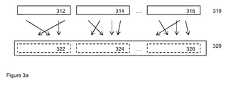
エラー訂正論理156が単一のコードワードを使用する場合には、バッファ152は、所定の位置ではないスクランブル解除を使用するために、メモリ110のサイズの2倍であるはずである。これは比較的コストがかかる。しかし、より小さいコードワードの訂正はリソースの効率をより増大させるので、エラー訂正では複数のコードワードを使用することが好適である。この場合、スクランブル動作は、コードワードの境界を考慮するように構成され得るが、例えば、より大きなバッファの使用または本明細書で記述される他の解決策の使用という他のオプションもある。図3aは、スクランブル動作を例示している。 If the
メモリコンテンツ310はコードワードサイズのメモリチャンクに分割される。図3aはそのような3つのチャンク312、314、316を示している。チャンクのそれぞれは、他のチャンクから独立してエラー訂正され得る。320では、メモリの同じ部分が図示されているが、メモリアクセスがスクランブルされている。矢印は、元のアドレスに対応したスクランブルされたアドレスを指している。このマッピングはコードワード境界を考慮していることに留意されたい。つまり、メモリアドレスのシーケンスは一連のメモリアドレスの複数のコードシーケンスを含み、アドレススクランブラー140は、1つの複数のコードシーケンスが異なるシーケンスのアドレスによってインターリーブされることなく、共に生成されるようにアドレスのシーケンスを生成する。そのようなアドレスのスクランブルによってサイドチャネルのリークの防止はより少なくなるが、著しい改善がある。図3bは、コードワード境界を考慮しないスクランブルされたメモリアクセス330を示している。このようなスクランブル関数では、リークをより防止できるが、図1のキー導出関数によって収容するのは(不可能ではないが)より困難である。図2に関連して以下で記述するシステムでは、2つのパスシステムを使用して、必ずしもコードワード境界を考慮する必要のない、スクランブルされたメモリアクセス330などのスクランブルされたメモリアクセスを処理できる。
並べ替え装置154を使用する代わりに、スクランブルをヘルパーデータと組み合わせの間に考慮に入れることも可能である。この場合、キー導出ユニット150は、バッファ152から、およびヘルパーデータメモリから(図1bではどちらも図示していない)読むコンバイナを含み得る。このアプローチではさらに、ヘルパーデータメモリは通常、不揮発性メモリで、通常、ブロック単位で読み出され、そのため、ヘルパーデータのランダムアクセスではよく、高い性能上のペナルティがつくという欠点がある。 As an alternative to using the
図2は、暗号化キーを生成するための改善された電子システム200を例示している。図4は、バリエーションが可能であるが、システム200を使用して行い得る暗号化キーを生成するための方法を流れ図で例示している。 FIG. 2 illustrates an improved
システム100と同様に、システム200は、メモリインタフェース120を通して、PUF制御ブロック210に接続されたPUFとして使用されるメモリ110を備えている。PUF制御ブロックは、メモリ読み出しユニット220およびキー導出ユニット230を備えている。 Similar to
メモリ読み出しユニット220は、事前に定義された順序で安全にメモリ110を読み出すように構成されている。事前に定義された順序は、後続のキー導出のために何が都合が良いかによって決められる。通常、事前に定義された順序は自然な線形順序であるが、任意の順序が可能である。例えば、難読化が増大している場合、ランダムであるが、固定された事前に定義された順序も選択され得、ヘルパーデータは、当該ランダムであるが、固定された事前に定義された順序にしたがって並べ替えられたメモリコンテンツに対して計算され得る。ここから、事前に定義された順序は線形であるものとするが、これは変更され得ることに留意していただきたい。メモリコンテンツは、メモリ110の電源投入によって取得され(ステップ410)、メモリはメモリコンテンツに確定される(ステップ420)。確定時間はメモリにより異なるが、必要に応じて、実験的に決められ得る。確定時間は通常、電子コンピューティングデバイスで通常、行われるブート機能よりもかなり短いので、通常、メモリの読み出しユニットのソフトウェア実装のためにメモリの読み出しを遅延させる遅延素子を導入することは必要とはされない。 Memory read
キー導出ユニット230は、メモリ110がメモリ読み出しユニット220から事前に定義された順序で確定したメモリコンテンツを受信する。一実施形態では、あるものは普通のPUF処理(エラー訂正および通常のキー導入関数)を行うように構成された、知られているキー導出ユニットを使用し得る。知られているキー導出ユニットが使用される場合には、キー導出ユニット230の観点から、これは通常のメモリコンテンツデータを受信する。こうして、システムのこの部分のみがおおまかな説明を与えられる。 The
キー導出ユニットはバッファ270を備え得る。バッファ270は単一のコードワードを保持できるほど大きい。キー導出関数は、ヘルパーデータメモリ285で記憶されたヘルパーデータとバッファのコンテンツを組み合わせるためのコンバイナ280を備え得る。組み合わせる関数は通常のビット単位の排他的論理和をとる動作であると想定する。しかし、任意の可逆なバイナリ動作が、例えば、異なるワード値の数を法として、例えば、バイトに対して256を法として使用され得る。ヘルパーデータはエラー訂正コードのコードワードとともにメモリコンテンツの事前に取得したコピーの排他的論理和をとることによって取得され得る。コードワードは秘密で、エラー訂正コードからランダムに選択されるか、または一部のキー管理スキームにしたがって選択される。動作中、コンバイナ280は秘密のコードワードに近傍にある訂正可能なビットストリングを取得するためにバッファ270で取得されるメモリコンテンツともにヘルパーデータの排他的論理和をとる。エラー訂正器290は、再度秘密のコードワードを取得するためにエラー訂正コードに対応するエラー訂正コードアルゴリズムを適用する。必要に応じて、キー導出関数ユニットは、キー導出関数(KDF)、例えば、暗号化ハッシュ関数などを適用する。暗号化関数は、任意の暗号化の目的、例えば、認証、暗号化などに使用され得る。 The key derivation unit may comprise a
興味深いことに、エラー訂正では、エラー訂正のためのツーパスシステムも同様に使用し得る。メモリはより小さなワードに分割され得、それは個別に、例えば、アダマールコードからコードワードへ訂正される。訂正されたより小さなコードワードは、より大きなブロックサイズエラー訂正コード、たとえばBCHコードで訂正されるより大きなワードへ組み合わされる。より大きなワードへの組み合わせはより小さなコードワードをインターリーブすることが好適である。キー導出関数は、訂正されたより小さなコードワードをメモリに暗号化された形で書き戻し得る。キー導出関数は、例えば、インターリーブを行うために、暗号化ユニットを使用して、メモリへのランダムアクセスを行い得る。このようにして、メモリ110はより複雑化したエラー訂正スキームのためのワーキングメモリとして使用され得、同時に引き続き、サイドチャネルのリークを低減化することができ、メモリ110が暗号化されると、暗号化および復号ユニットを通じて、ランダムアクセスの読み取り/書き込みアクセスをサポートする。 Interestingly, in error correction, a two-pass system for error correction can be used as well. The memory can be divided into smaller words, which are individually corrected, for example from Hadamard codes to code words. The corrected smaller codeword is combined into a larger word that is corrected with a larger block size error correction code, eg, a BCH code. It is preferable to interleave smaller codewords for larger word combinations. The key derivation function can write the corrected smaller codeword back into memory in encrypted form. The key derivation function may perform random access to the memory using, for example, an encryption unit to perform interleaving. In this way, the
キー導出ユニットは対応策を使用して、必要に応じて、サイドチャネルのリークを低減化し得る。例えば、WO2010/100015で記述されたデバイスおよび方法が使用され得る。 The key derivation unit may use countermeasures to reduce side channel leakage as needed. For example, the devices and methods described in WO2010 / 100015 can be used.
メモリ読み出しユニットは、スクランブルされた順序でメモリインタフェースを介してメモリコンテンツを取り出すためのアドレススクランブラー140、および暗号化ユニット240を備えている。暗号化ユニット240はスクランブラー140によって取り出されたデータを受信し、それを暗号化する。暗号化されたデータ、すなわち、暗号化されたメモリコンテンツがメモリに書き込まれる。任意のメモリが使用され得るが、暗号化されたメモリコンテンツはメモリ110に書き戻されることが好適である。必要とされるメモリ量を低減化するために、メモリコンテンツは同じスクランブルされた順序で書き戻され得る。それによって、メモリコンテンツが暗号されたメモリコンテンツで上書きされ、各暗号されたメモリワードは、読み出された同じスクランブルされたアドレスに書き戻される。暗号化ユニット240とスクランブルユニット140は共に、メモリを所定の場所、しかし、スクランブルされた順序で暗号化する効果があり得る。 The memory read unit comprises an
暗号化ユニット240はブロック暗号であり得る。例えば、暗号化ユニット240は、電子コードブックモード(ECB)で動作し得る。例えば、暗号化ユニット240は、カウンタモード(CTR)、例えば、アドレスをECBモードで暗号化して、メモリコンテンツへの結果の排他的論理和をとり動作し得る。ブロックサイズはよく非常に小さい、つまり、8、16、または32ビットなので、後者が好適である。その理由は、偶然に等しい値を有するメモリコンテンツのワード間の関係を曖昧にするからである。 The
暗号化ユニットではキーを必要とする。アドレススクランブラーでは、シード、またはアドレス暗号化が使用される場合にはキーが必要とされる。キーは固定され得るが、メモリ読み出しユニット220の起動時に作成されることがより好適である。キー/シードは、ランダムに、真または疑似ランダムのいずれかで作成され得る。例えば、メモリ読み出しユニット220は、真のランダム数発生器(図示せず)を含み得る。 The encryption unit requires a key. In the address scrambler, a key is required if seed or address encryption is used. Although the key can be fixed, it is more preferred that it be created when the memory read
しかし、ランダム性は通常、メモリ読み出しユニット220の電源投入の間にのみ必要とされることが観察されている。このことによって、図2で示されている別の解決策が可能になる。メモリ読み出しユニット220はさらなるメモリ260を備えている(PUF制御ブロック210内でメモリ110とは異なるものであることが好適である)。また、さらなるメモリ260も揮発性である。さらなるメモリの各電源投入時に、第2のメモリはノイズのあるメモリコンテンツに確定する。さらなるメモリのコンテンツはさらに物理的特性によっても異なるが、この目的のために、メモリコンテンツのノイズが利用されることに留意されたい。ランダムキーおよびシード導出ユニット265は、例えば、ハッシュ関数をメモリ260のコンテンツに適用することによって、メモリ265のメモリコンテンツからキーおよび/またはシードを導出する。例えば、後でメモリ110のコンテンツを再読み込みするために、新しいキー/シードが必要な場合には、新しく電源投入しなくても、新しいキーおよび新しいシードは、一方向性関数を古いシードに適用することによって取得され得る。 However, it has been observed that randomness is typically only required during power up of the memory read
メモリ読み出しユニット220はさらに、復号ユニット250およびアドレス生成器255を備えている。アドレス生成器255は、復号ユニット250と組み合わせられ得る。アドレス生成器255は、事前に定義された順序でメモリアドレスのシーケンスを作成するように構成されている。したがって、復号ユニット250は受信した暗号化されたメモリコンテンツを復号する。 The
こうして、安全な読み出しが2つのパスで得られる。第1のパスでは、メモリが暗号化状態にある。このパスは、より少なくサイドチャネルのリークにさらされる。その理由は、メモリへのアクセスがスクランブルされた順序だからである。第2のパスでは、メモリは、事前に定義された順序など、望ましい任意の順序で読み出される。第2のパスがより安全なのは、メモリインタフェースを介して渡されるすべてのデータが暗号化されているからである。システム100を上回るシステム200の利点は、任意のスクランブル関数がコードワード境界を考慮しなくても使用され得ることで、同時に、キー導出がより小さくサイズのコードワードでも引き続き機能し得ることである。 Thus, a safe read is obtained in two passes. In the first pass, the memory is in an encrypted state. This path is subject to less side channel leakage. This is because the access to the memory is in the scrambled order. In the second pass, the memory is read in any desired order, such as a predefined order. The second pass is more secure because all data passed through the memory interface is encrypted. The advantage of
システム100および200は、例えば、半導体デバイスなどの電子デバイスとして実装され得る。システム100および200は専用ハードウェアに実装され得る。システム100および200の一部はソフトウェアとして実装され得る。後者の場合、通常、システム、たとえば、PUF制御ブロックは、デバイスで格納される適切なソフトウェアを実行するマイクロプロセッサ(図示せず)を備え、例えば、ソフトウェアはダウンロードされ、対応するメモリ、例えば、RAM(図示せず)またはフラッシュなどの不揮発性メモリに記憶され得る。
図4は、暗号化キーを生成するための方法を流れ図で例示している。図4の方法は、バリエーションが可能であるが、システム200を使用して行われ得る。図4のステップ440、450、460、および470は方法のためのオプションで、例えば、システム100を使用して、省略され得る。 FIG. 4 illustrates in a flow diagram a method for generating an encryption key. The method of FIG. 4 can be varied using the
システム200の動作は、次のとおり行われ得る。最初に、システムに電源を投入する。(ステップ410)電源投入の間、メモリ110は電源投入され、メモリコンテンツで確定され得る(ステップ420)。メモリ110のメモリコンテンツは、ノイズがあり得るが、この特定のメモリの見本である。このメモリコンテンツの読み出しは、次の2つのパスで行われる。第1のパスで、メモリコンテンツは、たとえばステップ430のスクランブラーによって、スクランブルされた順序で取り出され(ステップ430)、たとえば暗号化ユニット240による暗号化のために受信される。メモリコンテンツは暗号化され(ステップ440)、書き戻される(ステップ450)。第2のパスで、暗号化されたメモリコンテンツは、事前に定義された順序、たとえば線形シーケンス順序で、たとえばアドレス生成器255によって取り出され、復号ユニット250によって受信される(ステップ460)。暗号化されたメモリコンテンツは、メモリ110が事前に定義された順序で確定したメモリコンテンツを取り出すために復号される(ステップ470)。 The operation of the
この点で、メモリコンテンツは、サイドチャネルのリークがない、または最低限で、メモリインタフェース120を介してメモリ110から安全に渡される。PUFの処理は、1つ以上の訂正可能なビットストリングを取得するためにメモリコンテンツとヘルパーデータを組み合わせることによって、進み得る。訂正可能なビットストリングは、エラー訂正コードの訂正可能な近傍にある。1つ以上の訂正可能なビットストリングは、エラー訂正アルゴリズムを使用してエラー訂正コードのコードワードを確立するためにエラー訂正され得る。キーは、KDFを適用することによって、確立されたコードワードから導出され得る。 In this regard, the memory content is safely passed from the
ステップ460および470で、メモリコンテンツは事前に定義された順序で取得される。このことは、メモリコンテンツが、特定の順序を必要とするヘルパーデータなどの、データと組み合わされる場合に望ましいものである。しかし、ステップ430、440、450、460、および470は、単なるPUFデータではなく、書き込み可能メモリから安全にすべてのデータを読み取るため、例えば、ステップ410、420、および/または480なしで、共に使用され得る。この場合、メモリコンテンツがステップ460および470において事前に定義された順序で受信される必要は必ずしもなく、代わりに、任意の望ましいさらなる順序も可能である。例えば、さらなる順序でメモリを安全に読み出すための方法は、請求項11のように暗号化キーの生成のために、スクランブルされた順序でメモリインタフェースからメモリコンテンツを受信し(430)、受信したメモリコンテンツを暗号化し(440)、暗号化されたメモリコンテンツをメモリに書き戻す(450)ことによってメモリを暗号化すること、およびさらなる順序で暗号化されたメモリコンテンツをメモリインタフェースから受信し(460)、さらなる順序でメモリコンテンツを取得するために受信した暗号化されたメモリコンテンツを復号する(470)ことによってメモリを復号することを含んでいる。 At steps 460 and 470, the memory content is obtained in a predefined order. This is desirable when memory content is combined with data, such as helper data that requires a specific order. However, steps 430, 440, 450, 460, and 470 are not just PUF data, but are used together, for example, without
方法400を実行するには多くの異なる方法が可能で、それは当業者には明らかになるであろう。例えば、ステップの順序は変更可能であり、一部のステップは並行して実行され得る。さらに、ステップの間に、他の方法ステップが挿入され得る。挿入されたステップは、本明細書で記述されているような方法の改善点を表すか、または本方法には関係しないものであり得る。例えば、ステップ470および480は、少なくとも部分的に平行して実行され得る。その上、所与のステップは、次のステップが開始される前に完全に完了しなくても構わない。 Many different ways of performing
本発明による方法はソフトウェアを使用して実行され得、これにはプロセッサシステムが方法400を実行できるようにするための命令が含まれる。ソフトウェアには、システムの特定のサブエンティティによって行われる当該ステップのみが含み得る。ソフトウェアは、ハードディスク、フロッピー(登録商標)、メモリなどの適切な記憶媒体に記憶され得る。ソフトウェアは、有線、または無線によって、あるいは、例えば、インターネットなどのデータネットワークを使用して送信され得る。ソフトウェアはダウンロードおよび/またはサーバ上でのリモート使用で使用可能にされ得る。 The method according to the present invention may be performed using software, including instructions for enabling a processor system to perform the
本発明はさらに、コンピュータプログラム、特に、本発明を実施するために適合されたキャリア上または中の特定のコンピュータプログラムに拡張していることを認識していただきたい。プログラムは、ソースコード、オブジェクトコード、コソースとオブジェクトの中間的コード、たとえば部分的にコンパイルされた形、または本発明による方法の実施での使用のために適切な他の任意の形であり得る。コンピュータプログラム製品に関連した一実施形態では、述べられた方法の少なくとも1つの処理ステップのそれぞれに対応するコンピュータ実行可能命令を備えている。これらの命令は、静的または動的にリンクされ得るサブルーチンに細分化および/または1つ以上のファイルに格納され得る。コンピュータプログラム製品に関連した別の実施形態では、述べられたシステムおよび/または製品の少なくとも1つの手段のそれぞれに対応するコンピュータ実行可能命令を備えている。 It should be appreciated that the present invention further extends to computer programs, and in particular to specific computer programs on or in a carrier adapted to implement the present invention. The program may be in source code, object code, co-source and object intermediate code, for example in partially compiled form, or any other form suitable for use in performing the method according to the invention. One embodiment relating to a computer program product comprises computer-executable instructions corresponding to each of the at least one processing step of the described method. These instructions can be subdivided into subroutines that can be linked statically or dynamically and / or stored in one or more files. Another embodiment relating to a computer program product comprises computer-executable instructions corresponding to each of the at least one means of the described system and / or product.
図5a〜図5dは、メモリのスクランブルおよび暗号化のための様々な可能性を例示している。簡単にするために、メモリの8つのメモリ位置が示されており、メモリコンテンツは少なくともこれら8つのメモリ位置を超えて拡張する。実際のところ、かなりより大きなメモリが使用され得る。図面では、メモリ位置は1から8の数字で示されている。メモリ位置は、例えば、8ビットワード、または16ビットワードなどのワードであり得、メモリアクセスへの読み取りアクセスは「R」で示され、書き込みアクセスは「W」で、難読化アクセスは「A」で示されている。難読化アクセスは、同じメモリ位置に対する読み取り、書き込み、または読み取りと書き込みの組み合わせとし得る。時間は左から右へと増大する。 Figures 5a to 5d illustrate various possibilities for memory scrambling and encryption. For simplicity, eight memory locations of memory are shown and the memory content extends beyond at least these eight memory locations. In fact, much larger memory can be used. In the drawing, memory locations are indicated by numbers from 1 to 8. The memory location can be, for example, a word such as an 8-bit word or a 16-bit word, read access to memory access is indicated by “R”, write access is “W”, and obfuscated access is “A”. It is shown in An obfuscated access can be a read, write, or a combination of read and write to the same memory location. Time increases from left to right.
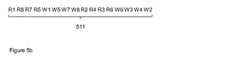
図5aでは、2つの段階、暗号化段階510および後続の復号段階520が示されている。暗号化段階の間、メモリ読み出しユニットは次を繰り返す。すなわち、メモリ位置から、すなわち、メモリアドレスから読み出して、メモリアドレスから読み出したコンテンツを暗号化し、そして同じメモリアドレスに書き戻す。メモリアドレスは、アドレススクランブラーによってスクランブルされている。暗号化段階510の最後に、メモリがスクランブルされた順序で読み出されても、メモリコンテンツ全体が暗号化されている。図5aで示されている特定のスクランブルされた順序は例示的なものである。 In FIG. 5a, two stages, an
復号段階の間、復号ユニットはさらなる順序で暗号化されたメモリコンテンツを受信した。図5aで使用されたさらにある順序は、自然なシーケンス順序である。通常、スクランブルされた順序は、同じデバイスの後続の電源投入が比較されると異なるが、さらなる順序は同じである。キー導出またはエラー訂正などの間に最善の性能を有するには、暗号化段階が終了後に復号段階520を開始するのが好適である。このことは、例えば、さらなる順序の第1のメモリ位置への暗号化された書き戻しが行われた後に、復号段階が当該位置の読み取りを開始し得、さらなる順序の次のメモリ位置で行われた後に、復号段階が1つのさらなる復号に続き得る場合には、必ずしも厳密に必要とされる訳ではない。この複雑さの増大は、難読化が追加の複雑さを犠牲にしても最大化する必要がある時にのみ、その価値があることになる。図5b〜図5dで、このことは行われないと想定すると、復号段階はそのため、図5aと同じであり、別個には示されていない。 During the decryption phase, the decryption unit received the memory content encrypted in a further order. One further order used in FIG. 5a is the natural sequence order. Usually, the scrambled order is different when subsequent power-ups of the same device are compared, but the further order is the same. In order to have the best performance, such as during key derivation or error correction, it is preferable to start the
暗号化段階がスクランブルされたメモリアドレスのシーケンスに対する読み取りおよび暗号化された書き戻しの繰り返されたサイクルを含む図5aの実施形態は、複数の異なるやり方に変化し得る。そのようなバリエーションは、新型の攻撃を防止するのに役立つ。 The embodiment of FIG. 5a, in which the encryption stage includes repeated cycles of read and encrypted writeback for a scrambled sequence of memory addresses, can vary in a number of different ways. Such variations can help prevent new types of attacks.
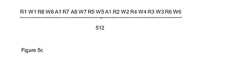
暗号化段階の間の読み取りおよび書き込みアクセスは厳密に交互である必要はない。例えば、暗号化段階は、複数のメモリコンテンツを読み取り、それらを暗号化して複数の暗号化されたメモリコンテンツを書き戻しうる。書き戻しが行われる順序は、同じか、または読み取られた順序と同じ場合も、または同じではない場合もある。暗号化された順序は、線形または再スクランブルされたものであり得る。図5bは暗号化段階511を示している。ここで、読み取りおよび書き込み動作は、この場合、それぞれ4つの読み取りおよび4つの書き込みという複数のバッチで行われる。バッチでは線形の書き戻しを使用し、第2のバッチはスクランブルされた書き戻しを使用する。バッチは、アドレスごとに、読み取り値とその暗号化を相関させることを難しくすることによって、5aの場合に対して改善される。 Read and write access during the encryption phase need not be strictly alternating. For example, the encryption stage may read a plurality of memory contents and encrypt them to write back a plurality of encrypted memory contents. The order in which writebacks are performed may or may not be the same as the order in which they were read. The encrypted order can be linear or re-scrambled. FIG. 5 b shows the
最近、光子放出攻撃は、アクセス中にSRAM構造のバックサイドから光子活動を記録することによって直接そのターゲットSRAMで威力が実証されている。光子放出攻撃は電子デバイスが、動作時に特定の確率で光子を放出する傾向にあるということに基づいている。光子の生成レートは、供給電圧およびトランジスタスイッチング周波数に比例する。特に、SRAM値の読み取りも光子の放出の原因となる。ICのバックサイドをCCDでねらう時、読み取り動作を記録することによってメモリコンテンツでの情報を収集することは可能である。光子放出解析は他の暗号解読方法および/またはサイドチャネルを支援し得る。 Recently, a photon emission attack has been demonstrated in its target SRAM directly by recording photon activity from the backside of the SRAM structure during access. Photon emission attacks are based on the fact that electronic devices tend to emit photons with a certain probability during operation. The photon generation rate is proportional to the supply voltage and the transistor switching frequency. In particular, reading the SRAM value also causes photon emission. When the backside of the IC is aimed at the CCD, it is possible to collect information on the memory contents by recording the reading operation. Photon emission analysis may support other decryption methods and / or side channels.
潜在的に、光子攻撃は、例えば、各PUF SRAMアドレスのまさに最初に読み取りを記録するためにSRAM PUFを攻撃するために使用され得るはずである。SRAMの電源投入のメモリコンテンツの読み出し全部が取得される場合、このことは深刻な安全上の問題になるはずである。例えば、光子放出の記録がすべてのまさに最初の読み取りをキャプチャし、SRAMからはそれ以上何もキャプチャせず、多くの回数、測定を繰り返すようにプログラムされる場合、SRAM開始値の信頼できるイメージが組み立てられ得るはずである。 Potentially, a photon attack could be used to attack a SRAM PUF, for example, to record a read at the very beginning of each PUF SRAM address. This should be a serious safety issue if all SRAM memory power-up reads are obtained. For example, if a record of photon emission captures all the very first readings, does not capture anything further from the SRAM, and is programmed to repeat the measurement many times, a reliable image of the SRAM start value is obtained. Should be able to be assembled.
それ自体での読み取り順序のスクランブルは光子攻撃に対処するために十分ではない、すなわち、ランダム化では、ピクチャは、順序に関係なく、単にすべての最初の読み取りアクションの総計なので、ピクチャを変更しないためである。幸い、図5aおよび、より少ない程度、5bでの読み出しでは、電源投入時にメモリが確定したメモリコンテンツに相関された読み出しには、それほど相関がない書き戻しが散在している。これによって、光子情報の使用はかなり困難になる。このセットアップを攻撃するために、攻撃者は(最初の)読み取りアクセスを選び出すためにシャッターメカニズムを使用し得る。シャッターは読み取り中は開いた位置および書き込み中は閉じた位置で構成される。このようにして、暗号化されない読み取りの間の光子放出のみが記録される。一実施形態では、メモリ読み出しユニットは少なくとも部分的にランダムでバッチサイズを選択するように構成され、暗号化ユニットにより暗号化されたバッチサイズ数の書き戻し動作が続く、アドレススクランブラーによるバッチサイズ数の読み取り動作を行うように構成されている。例えば、バッチサイズは起動時に選択され得るが、例えば、バッチサイズは各バッチサイズが読み取られた後などに繰り返し選択され得る。少なくとも部分的なランダムがPUFの一部に応じたバッチサイズを作成することで達成され得る。例えば、バッチサイズは、1、2、3、4バイトからランダムに選択され得る。 Scrambling of the read order on its own is not enough to deal with photon attacks, i.e., with randomization, the picture is simply the sum of all the first read actions, regardless of order, so it does not change the picture It is. Fortunately, in the read in FIG. 5a and to a lesser extent 5b, the read correlated with the memory content whose memory was determined at power-up is interspersed with less correlated writebacks. This makes the use of photon information quite difficult. To attack this setup, the attacker can use a shutter mechanism to pick out the (first) read access. The shutter is configured in an open position during reading and in a closed position during writing. In this way, only photon emissions during unencrypted readings are recorded. In one embodiment, the memory read unit is configured to select a batch size at least partially at random, followed by a write back operation of the batch size number encrypted by the encryption unit, the batch size number by the address scrambler. It is comprised so that reading operation | movement may be performed. For example, the batch size can be selected at startup, but for example, the batch size can be selected repeatedly, such as after each batch size is read. At least partial randomness can be achieved by creating a batch size that depends on a portion of the PUF. For example, the batch size can be selected randomly from 1, 2, 3, 4 bytes.
しかし、電源投入コンテンツに相関された信号をさらに低減化することが望ましい。 However, it is desirable to further reduce the signal correlated to the power-on content.
このことは、追加のランダム化されたアクセス、例えば、各メモリ位置への書き込みおよび/または読み取りを導入することで達成され得る。書き込みは最初の値を上書きするので、すべての後続の読み取りは混乱させるような情報を放出することになる。この対応策をより効果的なものにするために、アドレスごとに追加の書き込みおよび読み取りが他のアドレスと類似した書き込みおよび読み取りに対してランダムに順序付けされる必要がある。 This can be accomplished by introducing additional randomized access, eg, writing and / or reading to each memory location. Writing overwrites the initial value, so all subsequent readings will emit confusing information. In order to make this countermeasure more effective, additional writes and reads at each address need to be randomly ordered with respect to writes and reads similar to other addresses.
ランダム化された順序でのSRAMに対する追加の読み取りおよび書き込みを行うことで、最初のPUFデータの読み取りと分離することが難しいより多くの光子活動が生成される。追加の書き込みに使用されるデータはランダムデータ、固定されたパターン、またさらにデバイス固有のパターンであり得、ここで、PUFの一部はデバイス固有のパターンを導出するために使用される。さらに、これら3つの組み合わせも使用され得る。この順序のランダム化は、それ自体がPUF起動時に基づくランダムシードに基づき得る。ランダム化によって、すべてのメモリ位置で最初の時の読み取りアクセスを選び出すことが困難になる。 Performing additional reads and writes to the SRAM in randomized order produces more photon activity that is difficult to separate from reading the initial PUF data. The data used for additional writing can be random data, a fixed pattern, or even a device specific pattern, where a portion of the PUF is used to derive a device specific pattern. Furthermore, combinations of these three can also be used. This order randomization may be based on a random seed that is itself based upon PUF activation. Randomization makes it difficult to select the initial read access at all memory locations.
スクランブルされた読み出しおよび暗号化された書き込み準備ステップは、この攻撃を大いに阻害するために強化され得る。このことは、読み取り順序をスクランブルすることに加えて、読み出しおよび暗号化された書き戻し段階を併合することにより達成される。 The scrambled read and encrypted write preparation steps can be enhanced to greatly hinder this attack. This is accomplished by merging the read and encrypted writeback stages in addition to scrambling the read order.
暗号化されたデータの追加の読み取り、例えば、各アドレスからの数回の読み取り、最初の時の読み取りと後続の、例えば、PUFで得られたランダムシードに基づく、ランダム化での暗号化されたデータ読み取りを混合するなどを追加することによって、このスケジュールはそれぞれの電源投入で異なるので、攻撃者が読み取りおよび書き込みの正確なスケジュールを予測することは不可能である。その結果、SRAM起動値の信頼できるピクチャを作成することは非常に困難である。 Additional reading of encrypted data, eg several readings from each address, first time reading followed by randomization, eg, randomization based on random seed obtained with PUF It is impossible for an attacker to predict the exact schedule for reading and writing, because this schedule is different at each power-up, such as by adding a mix of data reads. As a result, it is very difficult to create a reliable picture of the SRAM startup value.
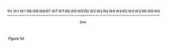
例えば、図5cの暗号化段階512は図510と同じスクランブルされた順序を示しているが、追加の難読化アクセスが追加されている。難読化アクセスは、例えば、読み出しユニット210に含まれる、難読化ユニットによって行われる。例えば、難読化ユニットは、ユニット210の残りの各読み取りおよび/または書き込みアクセスの後に難読化アクセスを挿入する機会を有し得る。図5cでは、難読化アクセスは、書き戻しが既に発生したメモリ位置にのみ行われる。 For example, the
異なるタイプのアクセスも利点となる。アクセスは、追加の読み取りにし得るはずである。これは、書き込みに必要な値についての不明点を回避するので、実施がより簡単である。アクセスは、読み取り/書き込みサイクルにし得るはずである。書き込みアクセスは、光子放出の原因になる可能性がより高いので、したがって、追加の難読化をもたらす。アクセスは、読み取り/書き込み/書き込みサイクルであり得るはずで、最初の書き込みでは、ランダム値または固定された値、たとえば、すべて1、または読み取り値の反転が書き込まれ、次いで、第2の書き込みでは、読み取られた値が書き戻される。これによって、メモリ位置でのスイッチが増大し、光子放出もさらに増大する。したがって、難読化アクセスの実行には、メモリ位置、すなわちアドレス、好適には、暗号化された書き込みが既に行われたものを選択すること、および選択されたメモリアドレスへのアクセスを行うことが含まれ得る。 Different types of access are also an advantage. Access could be an additional read. This is easier to implement because it avoids ambiguities about the values required for writing. The access could be a read / write cycle. Write access is more likely to cause photon emission, thus providing additional obfuscation. The access could be a read / write / write cycle, with the first write a random value or a fixed value, eg all 1s, or the inverse of the read value, and then the second write, The read value is written back. This increases the switch at the memory location and further increases the photon emission. Thus, performing an obfuscated access includes selecting a memory location, ie, an address, preferably one that has already been encrypted written, and performing an access to the selected memory address. Can be.
アクセスはさらに、書き込みアクセスでもあり得る可能性があり、後者の場合、訂正値が書き込まれることに注意する必要がある。実施の効果と容易さとの特定の優れたトレードオフが図5dに示されている。図5dで、暗号化段階は、複数の読み取り/書き戻しサイクルからなっている。書き込みは繰り返され、暗号化された(したがって、相関されない)書き戻しの光子効果が増大する。さらに、このシナリオでは、第1の書き込みはランダム、反転、固定とされ得るはずである。あいにく、図5dでは、シャッターを使用してRi選び出すために脆弱になる規則的なパターンRiWiWiを示しており、一実施形態では、読み取り/書き込みパターンはランダムなインターリーブで強化されている。例えば、書き込み動作の数は部分的にランダムになり得、例えば、上述のとおりバッチサイズ数が選択され得るが、バッチサイズ数は、書き戻しの繰り返しの数を制御するためにのみ使用される。他のランダムインターリーブも使用され得る。 Note that the access can also be a write access, in which case the correction value is written. A particular superior trade-off between the effectiveness and ease of implementation is shown in FIG. 5d. In FIG. 5d, the encryption phase consists of multiple read / write back cycles. Writing is repeated, increasing the photon effect of encrypted (and thus uncorrelated) writeback. Furthermore, in this scenario, the first write could be random, inverted, fixed. Unfortunately, FIG. 5d shows a regular pattern RiWiWi that is vulnerable to Ri selection using a shutter, and in one embodiment, the read / write pattern is enhanced with random interleaving. For example, the number of write operations can be partially random, for example, the batch size number can be selected as described above, but the batch size number is only used to control the number of write back iterations. Other random interleavings can also be used.
第1のものが暗号化された書き戻しの反転である2つの書き戻しを有することは、第1の読み取りで可能な光子放出の効果を低減化する光子放出を増大させる。 Having two writebacks where the first is the inverse of the encrypted writeback increases photon emission which reduces the effect of photon emission possible with the first read.
一実施形態では、難読化ユニットは、メモリのメモリ位置への難読化アクセスを行うように構成されており、難読化アクセスは暗号化ユニットが暗号化されたメモリコンテンツをメモリ位置に書き戻した後に行われる。難読化ユニットが、どのメモリ位置がアクセスに安全かを把握し得る種々のやり方がある。さらなる実施形態では、難読化アクセスは、復号ユニットがメモリ位置から暗号化されたメモリコンテンツを受信した前である。 In one embodiment, the obfuscation unit is configured to provide obfuscated access to a memory location of the memory, the obfuscation access after the encryption unit writes the encrypted memory content back to the memory location. Done. There are various ways in which the obfuscation unit can know which memory locations are safe for access. In a further embodiment, the obfuscated access is before the decryption unit receives the encrypted memory content from the memory location.
別の実施形態では、難読化ユニットはランダムなメモリ位置から読み取りアクセスを行う。暗号化段階の間の固定された地点で、たとえば、スクランブルされた各読み取り後および各書き戻し後に、難読化ユニットは、難読化アクセス、好適には、読み取りアクセスをランダムなメモリ位置に挿入する機会を有している。難読化ユニットは、難読化ユニットが難読化アクセスを挿入する確率を示す確率値を備えている。暗号化段階の開始時点で、確率値はより低い値であるが、少なくとも暗号化段階の間に、確率値は、暗号化段階の終了時点で、確率値が高い値であるように増大する。例えば、確率値は、固定された開始値から固定された終了値に、各機会の後に線形に増大し得る。 In another embodiment, the obfuscation unit provides read access from random memory locations. At a fixed point during the encryption phase, for example after each scrambled read and after each writeback, the obfuscation unit has the opportunity to insert an obfuscated access, preferably a read access, into a random memory location. have. The obfuscation unit has a probability value indicating the probability that the obfuscation unit will insert an obfuscated access. At the beginning of the encryption phase, the probability value is a lower value, but at least during the encryption phase, the probability value increases so that the probability value is a high value at the end of the encryption phase. For example, the probability value may increase linearly after each opportunity from a fixed start value to a fixed end value.
メモリのわずかな部分のみが暗号化される暗号化段階の最初では、追加の読み取りは攻撃者への信号を強化してしまうリスクがあるが、この段階では、読み取りの確率は低く、最後では、メモリの大部分が暗号化され、暗号化された値の読み取りの確率は高い。このスキームの利点は、どのメモリ位置が読み取りに安全か、すなわち、暗号化された値を有しているかを把握するための記憶処理が不必要であることである。一実施形態では、確率値は、暗号化段階の最初から最後まで線形に0.1から0.9に増大する。さらなる順序でメモリを安全に読み出すための電子メモリ読み出しユニットの一実施形態では、本明細書で記述された難読化ユニットのいずれか一つを備えている。 At the beginning of the encryption phase, when only a small portion of memory is encrypted, additional reads risk increasing the signal to the attacker, but at this stage, the probability of reading is low, and at the end, Most of the memory is encrypted and the probability of reading the encrypted value is high. The advantage of this scheme is that it does not require a storage process to know which memory locations are safe to read, i.e. have encrypted values. In one embodiment, the probability value increases linearly from 0.1 to 0.9 from the beginning to the end of the encryption phase. One embodiment of an electronic memory read unit for safely reading memory in a further order comprises any one of the obfuscation units described herein.
上述の実施形態は本発明を制限するものではなく、当業者が多くの代替の実施形態を設計できることを例示していることに留意すべきである。 It should be noted that the above-described embodiments are not intended to limit the present invention and illustrate that those skilled in the art can design many alternative embodiments.
請求項で、括弧間に配置されたすべての参照記号は、請求項を制限するものとして解釈されるべきではない。動詞「comprise(含む、備える)」およびその活用の使用は、請求項で述べられたもの以外の要素またはステップの存在を除外するものではない。要素の前の冠詞「a」または「an」は、そのような要素の複数の存在を除外するものでなない。本発明は、いくつかの別個の要素を備えるハードウェアによって、および適切にプログラミングされたコンピュータによって実装され得る。いくつかの手段を列挙するデバイスの請求項では、これらの手段のいくつかはハードウェアのいずれかおよび同じ要素によって具現化され得る。特定の方策が相互に異なる従属請求項で列挙されているということは、これらの手段の組み合わせは単に利点のために使用され得ないことを示してはいない。 In the claims, any reference signs placed between parentheses shall not be construed as limiting the claim. Use of the verb “comprise” and its conjugations does not exclude the presence of elements or steps other than those stated in a claim. The article “a” or “an” preceding an element does not exclude the presence of a plurality of such elements. The present invention may be implemented by hardware comprising several distinct elements and by a suitably programmed computer. In the device claim enumerating several means, several of these means can be embodied by one and the same element of hardware. The mere fact that certain measures are recited in mutually different dependent claims does not indicate that a combination of these measures cannot be used simply for advantage.
Claims (16)
Translated fromJapanese物理的クローン不能関数として使用されるメモリ(110)であって、メモリは書き込み可能で、揮発性であり、メモリに電源投入したたびに、メモリはメモリの少なくとも部分的にランダムな物理的特性に応じたメモリコンテンツに確定するように構成されており、メモリはメモリインタフェース(120)を通してアクセス可能であるメモリと、
メモリが確定したメモリコンテンツから暗号化キーを導出するように構成されたキー導出ユニット(150、230)とを備え、
暗号化キーを生成するための電子システムがさらに、
メモリインタフェースを通してメモリ、およびキー導出ユニットに接続されたメモリ読み出しユニット(220)を備え、メモリ読み出しユニットが
スクランブルされた順序でメモリインタフェースを介してメモリコンテンツを取り出すためのアドレススクランブラー(140)と、
メモリを暗号化するための暗号化ユニット(240)であって、メモリインタフェースからスクランブルされた順序でメモリコンテンツを受信し、受信したメモリコンテンツを暗号化し、暗号化されたメモリコンテンツをメモリに書き戻すように構成されている暗号化ユニット(240)と、
メモリを復号するための復号ユニット(250)であって、メモリインタフェースから事前に定義されたさらなる順序で暗号化されたメモリコンテンツを受信し、受信した暗号化されたメモリコンテンツを復号して事前に定義されたさらなる順序でメモリコンテンツを取得するように構成されている復号ユニット(250)と
を備える、電子システム。An electronic system (100, 200) for generating an encryption key comprising:
A memory (110) used as a physical non-clonal function, where the memory is writable and volatile, and each time the memory is powered on, the memory becomes at least partially random physical characteristics of the memory. A memory that is configured to determine the memory content according to the memory, wherein the memory is accessible through the memory interface (120);
A key derivation unit (150, 230) configured to derive an encryption key from the memory content with the determined memory,
An electronic system for generating the encryption key is further provided.
An address scrambler (140)comprising a memory read unit (220) connected to a memory and a key derivation unit through a memory interface, and for retrieving memory contents via the memory interface in the order in which the memory read unit is scrambled;
An encryption unit (240) for encrypting memory, which receives memory contents in a scrambled order from a memory interface, encrypts the received memory contents, and writes the encrypted memory contents back to the memory An encryption unit (240) configured as follows:
A decryption unit (250) for decrypting the memory, receiving memory content encrypted in a further predefined order from the memory interface, and decrypting the received encrypted memory content in advance A decryption unit (250) configured to obtain memory contents in a further defined order;
An electronic system comprising:
訂正可能なビットストリングを確立するためのコンバイナ(280)を備え、訂正可能なビットストリングはエラー訂正コードの訂正可能な近傍にあり、コンバイナ(280)が、ヘルパーデータメモリからヘルパーデータを取り出して、取り出したヘルパーデータと、メモリ読み出しユニットからされた事前に定義されたさらなる順序でメモリが確定したメモリコンテンツとを組み合わせるように構成され、さらに、
エラー訂正アルゴリズムを使用して訂正可能なビットストリングからエラー訂正コードのコードワードを確立するように構成されたエラーコレクタ(290)を備える、請求項1に記載の電子システム。Comprising a non-volatile helper data memory (285), wherein the helper data memory (285) stores helper data constructed for memory used as a physical non-clonal function;
A combiner (280) for establishing a correctable bit string, wherein the correctable bit string is in the correctable neighborhood of the error correction code, and the combiner (280) retrieves the helper data from the helper data memory; Configured to combine the retrieved helper data with the memory content determined from the memory read unit in a predefined further order, and
Comprising the configured error collector (290) to establish a codeword of an error correcting code from the correctable bit string using the error correction algorithm, the electronic system according to claim1.
物理的クローン不能関数として使用されるメモリ(110)であって、メモリは書き込み可能で、揮発性であり、メモリに電源投入したたびに、メモリはメモリの少なくとも部分的にランダムな物理的特性に応じたメモリコンテンツに確定するように構成されており、メモリはメモリインタフェース(120)を通してアクセス可能であるメモリと、
メモリが確定したメモリコンテンツから暗号化キーを導出するように構成されたキー導出ユニット(150、230)とを備え、電子メモリ読み出しユニットはメモリインタフェースを通してメモリ、およびキー導出ユニットに接続可能であり、電子メモリ読み出しユニットが、
スクランブルされた順序でメモリインタフェースを介してメモリコンテンツを取り出すように構成されたアドレススクランブラーと、
メモリを暗号化するための暗号化ユニットとを備え、暗号化ユニットが、メモリインタフェースからスクランブルされた順序でメモリコンテンツを受信し、受信したメモリコンテンツを暗号化し、暗号化されたメモリコンテンツをメモリに書き戻すように構成され、電子メモリ読み出しユニットがさらに、
メモリを復号するための復号ユニットを備え、復号ユニットが、メモリインタフェースから事前に定義されたさらなる順序で暗号化されたメモリコンテンツを受信し、受信した暗号化されたメモリコンテンツを復号して事前に定義されたさらなる順序でメモリコンテンツを取得するように構成された、電子メモリ読み出しユニット。In an electronic system (100, 200) for generating an encryption key, an electronic memory read unit for securely reading memoryin a furtherpredefined order, comprising:
A memory (110) used as a physical non-clonal function, where the memory is writable and volatile, and each time the memory is powered on, the memory becomes at least partially random physical characteristics of the memory. A memory that is configured to determine the memory content according to the memory, wherein the memory is accessible through the memory interface (120);
A key derivation unit (150, 230) configured to derive an encryption key from the memory content with the determined memory, the electronic memory readunit being connectable to the memoryand the key derivation unit through a memory interface; An electronic memory readout unit
An address scrambler configured to retrieve memory contents via the memory interface in a scrambled order;
An encryption unit for encrypting the memory, wherein the encryption unit receives the memory contents in the scrambled order from the memory interface, encrypts the received memory contents, and stores the encrypted memory contents in the memory. An electronic memory read unit is further configured to write back,
A decryption unit for decrypting the memory, wherein the decryption unit receives the memory content encryptedin a furtherpredefined order from the memory interface and decrypts the received encrypted memory content inadvance An electronic memory read unit configured to obtain memory contents ina furtherdefined order.
物理的クローン不能関数として使用されるメモリの電源投入するステップ(410)を含み、メモリが書き込み可能で揮発性であり、方法がさらに、
メモリが、メモリの少なくとも部分的にランダムな物理的特性に応じたメモリコンテンツに確定できるようにするステップ(420)、
スクランブルされた順序でメモリインタフェースを介してメモリコンテンツを取り出すステップ(430)、および
メモリが確定したメモリコンテンツから暗号化キーを導出するステップ(480)を含み、
メモリの暗号化が、
メモリインタフェースからスクランブルされた順序でメモリコンテンツを受信するステップ(430)、
受信したメモリコンテンツを暗号化するステップ(440)、および
暗号化されたメモリコンテンツをメモリに書き戻すステップ(450)によって行われること、
メモリの復号が、
メモリインタフェースから事前に定義されたさらなる順序で暗号化されたメモリコンテンツを受信するステップ(460)、および
事前に定義されたさらなる順序でメモリコンテンツを取得するために受信した暗号化されたメモリコンテンツを復号するステップ(470)によって行われることを含む方法。A method (400) for generating an encryption key, the method comprising:
Powering the memory used as a physical non-clonal function (410), wherein the memory is writable and volatile, and the method further comprises:
Enabling the memory to determine a memory content according to at least partially random physical characteristics of the memory (420);
Retrieving memory contents via the memory interface in scrambled order (430), andviewed including the step (480) for deriving an encryption key from the memory contents memory isdetermined,
Memory encryption
Receiving (430) memory contents in scrambled order from the memory interface;
Encrypting the received memory content (440); and
Performing the step (450) of writing the encrypted memory content back to the memory;
Memory decryption
Receiving (460) memory content encrypted in a further predefined order from the memory interface; and
A methodcomprising :performing (470) decrypting the received encrypted memory content to obtain the memory content in a further predefined order .
Applications Claiming Priority (5)
| Application Number | Priority Date | Filing Date | Title |
|---|---|---|---|
| EP12187213.9 | 2012-10-04 | ||
| EP12187213 | 2012-10-04 | ||
| EP12194713 | 2012-11-29 | ||
| EP12194713.9 | 2012-11-29 | ||
| PCT/EP2013/068746WO2014053286A1 (en) | 2012-10-04 | 2013-09-10 | System for generating a cryptographic key from a memory used as a physically unclonable function |
Publications (3)
| Publication Number | Publication Date |
|---|---|
| JP2015532549A JP2015532549A (en) | 2015-11-09 |
| JP2015532549A5 JP2015532549A5 (en) | 2016-10-20 |
| JP6267207B2true JP6267207B2 (en) | 2018-01-24 |
Family
ID=49118557
Family Applications (1)
| Application Number | Title | Priority Date | Filing Date |
|---|---|---|---|
| JP2015534947AActiveJP6267207B2 (en) | 2012-10-04 | 2013-09-10 | System for generating an encryption key from memory used as a physical non-clonal function |
Country Status (6)
| Country | Link |
|---|---|
| US (1) | US9430406B2 (en) |
| EP (1) | EP2904732B1 (en) |
| JP (1) | JP6267207B2 (en) |
| KR (1) | KR102201062B1 (en) |
| CN (1) | CN104704768B (en) |
| WO (1) | WO2014053286A1 (en) |
Families Citing this family (89)
| Publication number | Priority date | Publication date | Assignee | Title |
|---|---|---|---|---|
| DE102014208210A1 (en)* | 2014-04-30 | 2015-11-19 | Siemens Aktiengesellschaft | Derive a device-specific value |
| US10432409B2 (en) | 2014-05-05 | 2019-10-01 | Analog Devices, Inc. | Authentication system and device including physical unclonable function and threshold cryptography |
| US9946858B2 (en) | 2014-05-05 | 2018-04-17 | Analog Devices, Inc. | Authentication system and device including physical unclonable function and threshold cryptography |
| US9672342B2 (en) | 2014-05-05 | 2017-06-06 | Analog Devices, Inc. | System and device binding metadata with hardware intrinsic properties |
| IL234956A (en)* | 2014-10-02 | 2017-10-31 | Kaluzhny Uri | Bus protection with improved key entropy |
| US9640247B2 (en) | 2015-01-14 | 2017-05-02 | Qualcomm Incorporated | Methods and apparatuses for generating random numbers based on bit cell settling time |
| EP3046095B1 (en)* | 2015-01-15 | 2021-10-20 | Siemens Aktiengesellschaft | A method of protecting diverse applications stored on an integrated circuit using PUFs |
| EP3046096B1 (en)* | 2015-01-15 | 2022-03-30 | Siemens Aktiengesellschaft | A protection method of writting encrypted data to a memory device and reading decrypted data from the memory device using the power up of a PUF |
| US9425803B1 (en)* | 2015-05-07 | 2016-08-23 | The United States Of America As Represented By The Secretary Of The Navy | Apparatuses and methods for implementing various physically unclonable function (PUF) and random number generator capabilities |
| US9875378B2 (en) | 2015-06-12 | 2018-01-23 | QUALCOMOM Incorporated | Physically unclonable function assisted memory encryption device techniques |
| US10318431B2 (en) | 2015-09-17 | 2019-06-11 | Hewlett Packard Enterprise Development Lp | Obscuration of a cache signal |
| EP3147830B1 (en)* | 2015-09-23 | 2020-11-18 | Nxp B.V. | Protecting an integrated circuit |
| US20170126414A1 (en)* | 2015-10-28 | 2017-05-04 | Texas Instruments Incorporated | Database-less authentication with physically unclonable functions |
| EP3378054B1 (en)* | 2015-11-20 | 2021-03-17 | Intrinsic ID B.V. | Puf identifier assignment and testing method and device |
| DE102016201665A1 (en)* | 2016-02-03 | 2017-08-03 | Siemens Aktiengesellschaft | Encrypt the memory contents of a memory in an embedded system |
| US10572651B2 (en) | 2016-02-16 | 2020-02-25 | Samsung Electronics Co., Ltd. | Key generating method and apparatus using characteristic of memory |
| US10097348B2 (en)* | 2016-03-24 | 2018-10-09 | Samsung Electronics Co., Ltd. | Device bound encrypted data |
| US11843597B2 (en)* | 2016-05-18 | 2023-12-12 | Vercrio, Inc. | Automated scalable identity-proofing and authentication process |
| US10341122B2 (en)* | 2016-07-15 | 2019-07-02 | Hiroshi Watanabe | Electronic appliance and network of the same |
| US10680809B2 (en) | 2016-08-04 | 2020-06-09 | Macronix International Co., Ltd. | Physical unclonable function for security key |
| US10855477B2 (en) | 2016-08-04 | 2020-12-01 | Macronix International Co., Ltd. | Non-volatile memory with physical unclonable function and random number generator |
| US10404478B2 (en) | 2016-08-04 | 2019-09-03 | Macronix International Co., Ltd. | Physical unclonable function using divided threshold distributions in non-volatile memory |
| US11258599B2 (en) | 2016-08-04 | 2022-02-22 | Macronix International Co., Ltd. | Stable physically unclonable function |
| US10911229B2 (en) | 2016-08-04 | 2021-02-02 | Macronix International Co., Ltd. | Unchangeable physical unclonable function in non-volatile memory |
| CN106301786B (en)* | 2016-08-10 | 2019-04-02 | 南京航空航天大学 | A kind of physics unclonable function response error correction circuit based on SRAM type memory |
| US10318748B2 (en)* | 2016-09-30 | 2019-06-11 | Intel Corporation | Techniques to protect fuses against non-destructive attacks |
| US10387660B1 (en)* | 2016-10-17 | 2019-08-20 | National Technology & Engineering Solutions Of Sandia, Llc | Computational optical physical unclonable function |
| US10394492B2 (en)* | 2016-10-26 | 2019-08-27 | Lenovo Enterprise Solutions (Singapore) Pte. Ltd. | Securing a media storage device using write restriction mechanisms |
| US9811689B1 (en) | 2016-12-27 | 2017-11-07 | Macronix International Co., Ltd. | Chip ID generation using physical unclonable function |
| US10082975B1 (en) | 2017-03-02 | 2018-09-25 | Micron Technology, Inc. | Obfuscation-enhanced memory encryption |
| JP6882666B2 (en)* | 2017-03-07 | 2021-06-02 | 富士通株式会社 | Key generator and key generator |
| CN106933752B (en)* | 2017-03-09 | 2019-10-08 | 西安电子科技大学 | A kind of encryption device and method of SRAM type FPGA |
| US11522725B2 (en)* | 2017-03-29 | 2022-12-06 | Board Of Regents, The University Of Texas System | Reducing amount of helper data in silicon physical unclonable functions via lossy compression without production-time error characterization |
| KR101974465B1 (en)* | 2017-05-25 | 2019-08-23 | 한밭대학교 산학협력단 | Noise coupled physical unclonable functions system |
| US10425235B2 (en) | 2017-06-02 | 2019-09-24 | Analog Devices, Inc. | Device and system with global tamper resistance |
| US10958452B2 (en) | 2017-06-06 | 2021-03-23 | Analog Devices, Inc. | System and device including reconfigurable physical unclonable functions and threshold cryptography |
| US11093588B2 (en)* | 2017-06-26 | 2021-08-17 | Micron Technology, Inc. | Memory system including data obfuscation |
| CN107196766B (en)* | 2017-07-20 | 2023-04-14 | 中国工程物理研究院电子工程研究所 | A Miniaturized Quantum Authentication System |
| EP3435586B1 (en)* | 2017-07-25 | 2019-08-07 | Intrinsic ID B.V. | Method to reduce aging of a cache memory |
| US10949546B2 (en) | 2017-08-02 | 2021-03-16 | Samsung Electronics Co., Ltd. | Security devices, electronic devices and methods of operating electronic devices |
| US10649735B2 (en)* | 2017-09-12 | 2020-05-12 | Ememory Technology Inc. | Security system with entropy bits |
| CN107908980B (en)* | 2017-10-10 | 2021-11-23 | 芯海科技(深圳)股份有限公司 | Method for realizing encryption protection of memory data |
| US11050574B2 (en)* | 2017-11-29 | 2021-06-29 | Taiwan Semiconductor Manufacturing Company, Ltd. | Authentication based on physically unclonable functions |
| CN108229215A (en)* | 2017-12-06 | 2018-06-29 | 杭州中天微系统有限公司 | A kind of scrambled storage device in address and method |
| CN108182371A (en)* | 2017-12-22 | 2018-06-19 | 杭州中天微系统有限公司 | The chip external memory address scrambling apparatus and method of a kind of system on chip |
| CN110018810B (en)* | 2018-01-10 | 2021-05-18 | 力旺电子股份有限公司 | random code generator |
| CN111630598B (en)* | 2018-01-23 | 2023-04-11 | 新唐科技日本株式会社 | Nonvolatile memory device and writing method thereof |
| US11265151B2 (en)* | 2018-03-09 | 2022-03-01 | Arizona Board Of Regents On Behalf Of Northern Arizona University | Key exchange schemes with addressable elements |
| JP6752247B2 (en) | 2018-03-09 | 2020-09-09 | 三菱重工業株式会社 | Information distribution device, distribution target device, information distribution system, information distribution method and program |
| EP3562092A1 (en)* | 2018-04-26 | 2019-10-30 | Thales Dis Design Services Sas | Method for generating on-board a cryptographic key using a physically unclonable function |
| GB201806997D0 (en)* | 2018-04-30 | 2018-06-13 | Univ Leuven Kath | Configurable hardware device |
| US10742406B2 (en) | 2018-05-03 | 2020-08-11 | Micron Technology, Inc. | Key generation and secure storage in a noisy environment |
| US11063755B2 (en) | 2018-05-07 | 2021-07-13 | Cryptography Research, Inc. | Generating a key at a device based on a memory of the device |
| US12013751B2 (en) | 2018-06-11 | 2024-06-18 | Cryptography Research, Inc. | Generating a target data based on a function associated with a physical variation of a device |
| US11113422B2 (en) | 2018-08-03 | 2021-09-07 | Micron Technology, Inc. | Data protection in computer processors |
| US11074198B2 (en) | 2018-09-18 | 2021-07-27 | Micron Technology, Inc. | Key management in computer processors |
| US11303462B2 (en) | 2018-11-19 | 2022-04-12 | Arizona Board Of Regents On Behalf Of Northern Arizona University | Unequally powered cryptography using physical unclonable functions |
| KR102263877B1 (en)* | 2018-12-18 | 2021-06-14 | 시큐리티플랫폼 주식회사 | Unique encryption key generator for device and method thereof |
| CN109656840A (en)* | 2018-12-21 | 2019-04-19 | 成都海光集成电路设计有限公司 | A kind of device of data encrypting and deciphering, method, storage medium and data-storage system |
| US11233662B2 (en)* | 2018-12-26 | 2022-01-25 | Arizona Board Of Regents On Behalf Of Northern Arizona University | Keyless encrypting schemes using physical unclonable function devices |
| TWI734314B (en)* | 2018-12-31 | 2021-07-21 | 美商美光科技公司 | Systems, methods and non-transitory computer-readable medium for providing a digital fingerprint to a host device |
| US11514174B2 (en)* | 2019-01-23 | 2022-11-29 | Micron Technology, Inc. | Memory devices with cryptographic components |
| US11218330B2 (en) | 2019-03-25 | 2022-01-04 | Micron Technology, Inc. | Generating an identity for a computing device using a physical unclonable function |
| US11323275B2 (en) | 2019-03-25 | 2022-05-03 | Micron Technology, Inc. | Verification of identity using a secret key |
| KR102169468B1 (en) | 2019-05-20 | 2020-10-23 | 충북대학교 산학협력단 | Challenge scrambler for physical unclonable function |
| US11841983B2 (en)* | 2019-06-07 | 2023-12-12 | Ohio State Innovation Foundation | Systems and methods using hybrid Boolean networks as physically unclonable functions |
| US11343108B2 (en)* | 2019-06-12 | 2022-05-24 | Arizona Board Of Regents On Behalf Of Northern Arizona University | Generation of composite private keys |
| US11483167B2 (en) | 2019-06-20 | 2022-10-25 | Intel Corporation | Method and apparatus to provide memory based physically unclonable functions |
| US11194978B2 (en)* | 2019-07-12 | 2021-12-07 | Northrop Grumman Systems Corporation | Combined radio frequency identification (RFID)-based asset management and component authentication |
| US20210051010A1 (en)* | 2019-08-16 | 2021-02-18 | PUFsecurity Corporation | Memory Device Providing Data Security |
| JP7560535B2 (en)* | 2019-10-08 | 2024-10-02 | クリプトグラフィ リサーチ, インコーポレイテッド | Encryption Physical Unclonable Function Circuit Helper Data |
| GB201919297D0 (en) | 2019-12-24 | 2020-02-05 | Aronson Bill | Temperature sensing physical unclonable function (puf) authenication system |
| US11516028B2 (en) | 2019-12-24 | 2022-11-29 | CERA Licensing Limited | Temperature sensing physical unclonable function (PUF) authentication system |
| KR102833051B1 (en) | 2020-04-20 | 2025-07-11 | 삼성전자주식회사 | Memory modules and semiconductor memory devices |
| US12184795B2 (en)* | 2020-06-26 | 2024-12-31 | Taiwan Semiconductor Manufacturing Company, Ltd. | PUF method and structure |
| CN112104459B (en)* | 2020-09-10 | 2023-05-12 | 国网江苏省电力有限公司信息通信分公司 | Key generation method based on channel fingerprint and auxiliary data |
| US11380379B2 (en) | 2020-11-02 | 2022-07-05 | Macronix International Co., Ltd. | PUF applications in memories |
| US11604740B2 (en)* | 2020-12-01 | 2023-03-14 | Capital One Services, Llc | Obfuscating cryptographic material in memory |
| CN113037488B (en)* | 2021-04-19 | 2022-07-22 | 工业信息安全(四川)创新中心有限公司 | Format-preserving encryption method and decryption method based on cryptographic hash algorithm |
| US12255994B2 (en)* | 2021-06-07 | 2025-03-18 | Micron Technology, Inc. | Secure data storage with a dynamically generated key |
| US20230038135A1 (en)* | 2021-07-23 | 2023-02-09 | Arizona Board Of Regents On Behalf Of Northern Arizona University | Salted hashing method for response-based cryptography |
| US12166876B2 (en)* | 2021-07-30 | 2024-12-10 | Micron Technology, Inc. | Embedded hardware security module (HSM) |
| WO2023107287A1 (en)* | 2021-12-06 | 2023-06-15 | Cryptography Research, Inc. | Physically uncloneable function as secure storage |
| US12166870B2 (en)* | 2022-04-20 | 2024-12-10 | Micron Technology, Inc. | Physical unclonable function failure protection and prediction |
| US12013970B2 (en) | 2022-05-16 | 2024-06-18 | Bank Of America Corporation | System and method for detecting and obfuscating confidential information in task logs |
| CN114912154B (en)* | 2022-06-06 | 2024-03-15 | 山东大学 | An implementation method of integrating encryption, storage and calculation based on non-volatile memory |
| CN115216861B (en)* | 2022-07-22 | 2023-07-28 | 河南大学 | PUF device based on metal-dielectric-luminous coaxial multilayer composite nanofiber and method for generating secret key by using device |
| US20240195635A1 (en)* | 2022-12-12 | 2024-06-13 | Intel Corporation | Roots of trust in intellectual property (ip) blocks in a system on a chip (soc) |
| WO2025047724A1 (en)* | 2023-08-31 | 2025-03-06 | ヌヴォトンテクノロジージャパン株式会社 | Semiconductor integrated circuit and data transfer method |
Family Cites Families (9)
| Publication number | Priority date | Publication date | Assignee | Title |
|---|---|---|---|---|
| US7310706B1 (en)* | 2001-06-01 | 2007-12-18 | Mips Technologies, Inc. | Random cache line refill |
| JP2003018143A (en)* | 2001-06-28 | 2003-01-17 | Mitsubishi Electric Corp | Information processing equipment |
| RU2007144715A (en) | 2005-06-01 | 2009-06-10 | Конинклейке Филипс Электроникс Н.В. (Nl) | UPDATE TEMPLATE IN ASSISTANT DATA SYSTEMS |
| IL187046A0 (en)* | 2007-10-30 | 2008-02-09 | Sandisk Il Ltd | Memory randomization for protection against side channel attacks |
| US8638931B2 (en)* | 2007-10-30 | 2014-01-28 | Spansion Llc | Signal descrambling detector |
| EP2359520B1 (en)* | 2008-11-17 | 2019-08-14 | Intrinsic ID B.V. | Distributed puf |
| EP2404403B1 (en)* | 2009-03-06 | 2019-12-04 | Intrinsic ID B.V. | System for establishing a cryptographic key depending on a physical system |
| CN102656588B (en)* | 2009-08-14 | 2015-07-15 | 本质Id有限责任公司 | Physically unclonable function with tamper prevention and anti-aging system |
| WO2011088074A2 (en) | 2010-01-12 | 2011-07-21 | Stc. Unm | System and methods for generating unclonable security keys in integrated circuits |
- 2013
- 2013-09-10USUS14/426,728patent/US9430406B2/enactiveActive
- 2013-09-10JPJP2015534947Apatent/JP6267207B2/enactiveActive
- 2013-09-10CNCN201380052311.6Apatent/CN104704768B/enactiveActive
- 2013-09-10EPEP13759256.4Apatent/EP2904732B1/enactiveActive
- 2013-09-10KRKR1020157011155Apatent/KR102201062B1/enactiveActive
- 2013-09-10WOPCT/EP2013/068746patent/WO2014053286A1/enactiveApplication Filing
Also Published As
| Publication number | Publication date |
|---|---|
| EP2904732B1 (en) | 2018-11-28 |
| EP2904732A1 (en) | 2015-08-12 |
| JP2015532549A (en) | 2015-11-09 |
| US9430406B2 (en) | 2016-08-30 |
| US20150234751A1 (en) | 2015-08-20 |
| WO2014053286A1 (en) | 2014-04-10 |
| KR20150064148A (en) | 2015-06-10 |
| CN104704768B (en) | 2018-01-05 |
| CN104704768A (en) | 2015-06-10 |
| KR102201062B1 (en) | 2021-01-11 |
Similar Documents
| Publication | Publication Date | Title |
|---|---|---|
| JP6267207B2 (en) | System for generating an encryption key from memory used as a physical non-clonal function | |
| CN108449172B (en) | Encryption/decryption method and integrated circuit of computing device | |
| US8726040B2 (en) | Memory randomization for protection against side channel attacks | |
| US11728967B2 (en) | Dynamic masking | |
| US10187200B1 (en) | System and method for generating a multi-stage key for use in cryptographic operations | |
| JP5306465B2 (en) | Pre-calculation of message authentication code applied to secure memory | |
| EP2695052B1 (en) | Random number generating system based on memory start-up noise | |
| US8767959B2 (en) | Block encryption | |
| JP5167374B2 (en) | Data encryption device and memory card | |
| JP2017504838A (en) | Countermeasures against side-channel attacks against cryptographic algorithms | |
| CN107078904A (en) | Hybrid cryptographic key derivation | |
| JP2019145082A (en) | Countermeasures against phase tracking attacks on ring oscillator based entropy sources | |
| CN104704501A (en) | Securely generating and storing passwords in computer system | |
| WO2007026287A1 (en) | Method and device for generating random number generator seeds | |
| US9391770B2 (en) | Method of cryption | |
| JP2019122046A (en) | Entanglement and recall system using physically unclonable function technology | |
| CN109902492B (en) | Method for writing encryption information set in integrated circuit external memory and integrated circuit | |
| US12341871B2 (en) | Practical itemized encryption for cryptographic erasure (PIECE) | |
| Kirkpatrick et al. | PUF ROKs: generating read-once keys from physically unclonable functions | |
| Gong et al. | Practical Opcode-based Fault Attack on AES-NI | |
| Braga et al. | Integrated technologies for communication security and secure deletion on android smartphones | |
| Ramkumar | DOWN with trusted devices |
Legal Events
| Date | Code | Title | Description |
|---|---|---|---|
| A521 | Request for written amendment filed | Free format text:JAPANESE INTERMEDIATE CODE: A523 Effective date:20160829 | |
| A621 | Written request for application examination | Free format text:JAPANESE INTERMEDIATE CODE: A621 Effective date:20160829 | |
| A977 | Report on retrieval | Free format text:JAPANESE INTERMEDIATE CODE: A971007 Effective date:20170726 | |
| A131 | Notification of reasons for refusal | Free format text:JAPANESE INTERMEDIATE CODE: A131 Effective date:20170815 | |
| A521 | Request for written amendment filed | Free format text:JAPANESE INTERMEDIATE CODE: A523 Effective date:20171102 | |
| TRDD | Decision of grant or rejection written | ||
| A01 | Written decision to grant a patent or to grant a registration (utility model) | Free format text:JAPANESE INTERMEDIATE CODE: A01 Effective date:20171205 | |
| A61 | First payment of annual fees (during grant procedure) | Free format text:JAPANESE INTERMEDIATE CODE: A61 Effective date:20171221 | |
| R150 | Certificate of patent or registration of utility model | Ref document number:6267207 Country of ref document:JP Free format text:JAPANESE INTERMEDIATE CODE: R150 | |
| R250 | Receipt of annual fees | Free format text:JAPANESE INTERMEDIATE CODE: R250 | |
| R250 | Receipt of annual fees | Free format text:JAPANESE INTERMEDIATE CODE: R250 | |
| R250 | Receipt of annual fees | Free format text:JAPANESE INTERMEDIATE CODE: R250 | |
| R250 | Receipt of annual fees | Free format text:JAPANESE INTERMEDIATE CODE: R250 | |
| R250 | Receipt of annual fees | Free format text:JAPANESE INTERMEDIATE CODE: R250 |