JP6261352B2 - Carbon nanotube sheet, semiconductor device, method of manufacturing carbon nanotube sheet, and method of manufacturing semiconductor device - Google Patents
Carbon nanotube sheet, semiconductor device, method of manufacturing carbon nanotube sheet, and method of manufacturing semiconductor deviceDownload PDFInfo
- Publication number
- JP6261352B2 JP6261352B2JP2014010306AJP2014010306AJP6261352B2JP 6261352 B2JP6261352 B2JP 6261352B2JP 2014010306 AJP2014010306 AJP 2014010306AJP 2014010306 AJP2014010306 AJP 2014010306AJP 6261352 B2JP6261352 B2JP 6261352B2
- Authority
- JP
- Japan
- Prior art keywords
- carbon nanotube
- resin portion
- thermoplastic resin
- thermosetting resin
- sheet
- Prior art date
- Legal status (The legal status is an assumption and is not a legal conclusion. Google has not performed a legal analysis and makes no representation as to the accuracy of the status listed.)
- Active
Links
- OKTJSMMVPCPJKN-UHFFFAOYSA-NCarbonChemical compound[C]OKTJSMMVPCPJKN-UHFFFAOYSA-N0.000titleclaimsdescription223
- 239000002041carbon nanotubeSubstances0.000titleclaimsdescription222
- 229910021393carbon nanotubeInorganic materials0.000titleclaimsdescription222
- 239000004065semiconductorSubstances0.000titleclaimsdescription86
- 238000004519manufacturing processMethods0.000titleclaimsdescription24
- 229920005989resinPolymers0.000claimsdescription105
- 239000011347resinSubstances0.000claimsdescription105
- 229920005992thermoplastic resinPolymers0.000claimsdescription100
- 229920001187thermosetting polymerPolymers0.000claimsdescription95
- 239000000463materialSubstances0.000claimsdescription34
- 230000002093peripheral effectEffects0.000claimsdescription31
- 239000000758substrateSubstances0.000claimsdescription21
- 238000010438heat treatmentMethods0.000claimsdescription7
- 238000003825pressingMethods0.000claimsdescription6
- 238000005498polishingMethods0.000claimsdescription4
- 239000002071nanotubeSubstances0.000claimsdescription2
- 229910052799carbonInorganic materials0.000claims1
- XUIMIQQOPSSXEZ-UHFFFAOYSA-NSiliconChemical compound[Si]XUIMIQQOPSSXEZ-UHFFFAOYSA-N0.000description14
- 229910052710siliconInorganic materials0.000description14
- 239000010703siliconSubstances0.000description14
- 239000000853adhesiveSubstances0.000description8
- 230000001070adhesive effectEffects0.000description8
- 230000017525heat dissipationEffects0.000description8
- 229910052751metalInorganic materials0.000description8
- 239000002184metalSubstances0.000description8
- 238000000034methodMethods0.000description8
- 239000003054catalystSubstances0.000description6
- 230000003197catalytic effectEffects0.000description5
- 239000007789gasSubstances0.000description4
- 229910052738indiumInorganic materials0.000description4
- APFVFJFRJDLVQX-UHFFFAOYSA-Nindium atomChemical compound[In]APFVFJFRJDLVQX-UHFFFAOYSA-N0.000description4
- XEEYBQQBJWHFJM-UHFFFAOYSA-NIronChemical compound[Fe]XEEYBQQBJWHFJM-UHFFFAOYSA-N0.000description3
- PXHVJJICTQNCMI-UHFFFAOYSA-NNickelChemical compound[Ni]PXHVJJICTQNCMI-UHFFFAOYSA-N0.000description3
- 230000015572biosynthetic processEffects0.000description3
- 239000010419fine particleSubstances0.000description3
- 239000004519greaseSubstances0.000description3
- 230000020169heat generationEffects0.000description3
- BASFCYQUMIYNBI-UHFFFAOYSA-NplatinumChemical compound[Pt]BASFCYQUMIYNBI-UHFFFAOYSA-N0.000description3
- 230000005855radiationEffects0.000description3
- XKRFYHLGVUSROY-UHFFFAOYSA-NArgonChemical compound[Ar]XKRFYHLGVUSROY-UHFFFAOYSA-N0.000description2
- RYGMFSIKBFXOCR-UHFFFAOYSA-NCopperChemical compound[Cu]RYGMFSIKBFXOCR-UHFFFAOYSA-N0.000description2
- 238000005229chemical vapour depositionMethods0.000description2
- 239000004020conductorSubstances0.000description2
- 229910052802copperInorganic materials0.000description2
- 239000010949copperSubstances0.000description2
- 239000010931goldSubstances0.000description2
- 239000007788liquidSubstances0.000description2
- 238000003303reheatingMethods0.000description2
- 229910000679solderInorganic materials0.000description2
- 238000002230thermal chemical vapour depositionMethods0.000description2
- 239000004743PolypropyleneSubstances0.000description1
- VYPSYNLAJGMNEJ-UHFFFAOYSA-NSilicium dioxideChemical compoundO=[Si]=OVYPSYNLAJGMNEJ-UHFFFAOYSA-N0.000description1
- BQCADISMDOOEFD-UHFFFAOYSA-NSilverChemical compound[Ag]BQCADISMDOOEFD-UHFFFAOYSA-N0.000description1
- HSFWRNGVRCDJHI-UHFFFAOYSA-Nalpha-acetyleneNatural productsC#CHSFWRNGVRCDJHI-UHFFFAOYSA-N0.000description1
- 229910052786argonInorganic materials0.000description1
- 239000000919ceramicSubstances0.000description1
- 239000011248coating agentSubstances0.000description1
- 238000000576coating methodMethods0.000description1
- 229910017052cobaltInorganic materials0.000description1
- 239000010941cobaltSubstances0.000description1
- GUTLYIVDDKVIGB-UHFFFAOYSA-Ncobalt atomChemical compound[Co]GUTLYIVDDKVIGB-UHFFFAOYSA-N0.000description1
- 238000009833condensationMethods0.000description1
- 230000005494condensationEffects0.000description1
- 238000010586diagramMethods0.000description1
- 239000003822epoxy resinSubstances0.000description1
- 125000002534ethynyl groupChemical group[H]C#C*0.000description1
- 230000008020evaporationEffects0.000description1
- 238000001704evaporationMethods0.000description1
- 239000011521glassSubstances0.000description1
- PCHJSUWPFVWCPO-UHFFFAOYSA-NgoldChemical compound[Au]PCHJSUWPFVWCPO-UHFFFAOYSA-N0.000description1
- 229910052737goldInorganic materials0.000description1
- 229910052742ironInorganic materials0.000description1
- 239000002923metal particleSubstances0.000description1
- 230000004048modificationEffects0.000description1
- 238000012986modificationMethods0.000description1
- 229910052759nickelInorganic materials0.000description1
- 229910052697platinumInorganic materials0.000description1
- 229920000647polyepoxidePolymers0.000description1
- 229920013716polyethylene resinPolymers0.000description1
- 229920001721polyimidePolymers0.000description1
- 239000009719polyimide resinSubstances0.000description1
- -1polypropylenePolymers0.000description1
- 229920001155polypropylenePolymers0.000description1
- 239000002994raw materialSubstances0.000description1
- 229910052814silicon oxideInorganic materials0.000description1
- 229910052709silverInorganic materials0.000description1
- 239000004332silverSubstances0.000description1
- 238000004544sputter depositionMethods0.000description1
Images


Classifications
- C—CHEMISTRY; METALLURGY
- C09—DYES; PAINTS; POLISHES; NATURAL RESINS; ADHESIVES; COMPOSITIONS NOT OTHERWISE PROVIDED FOR; APPLICATIONS OF MATERIALS NOT OTHERWISE PROVIDED FOR
- C09K—MATERIALS FOR MISCELLANEOUS APPLICATIONS, NOT PROVIDED FOR ELSEWHERE
- C09K5/00—Heat-transfer, heat-exchange or heat-storage materials, e.g. refrigerants; Materials for the production of heat or cold by chemical reactions other than by combustion
- C09K5/08—Materials not undergoing a change of physical state when used
- C09K5/14—Solid materials, e.g. powdery or granular
- H—ELECTRICITY
- H01—ELECTRIC ELEMENTS
- H01L—SEMICONDUCTOR DEVICES NOT COVERED BY CLASS H10
- H01L23/00—Details of semiconductor or other solid state devices
- H01L23/34—Arrangements for cooling, heating, ventilating or temperature compensation ; Temperature sensing arrangements
- H01L23/36—Selection of materials, or shaping, to facilitate cooling or heating, e.g. heatsinks
- H01L23/373—Cooling facilitated by selection of materials for the device or materials for thermal expansion adaptation, e.g. carbon
- H01L23/3737—Organic materials with or without a thermoconductive filler
- H—ELECTRICITY
- H01—ELECTRIC ELEMENTS
- H01L—SEMICONDUCTOR DEVICES NOT COVERED BY CLASS H10
- H01L23/00—Details of semiconductor or other solid state devices
- H01L23/34—Arrangements for cooling, heating, ventilating or temperature compensation ; Temperature sensing arrangements
- H01L23/42—Fillings or auxiliary members in containers or encapsulations selected or arranged to facilitate heating or cooling
- H01L23/433—Auxiliary members in containers characterised by their shape, e.g. pistons
- H—ELECTRICITY
- H01—ELECTRIC ELEMENTS
- H01L—SEMICONDUCTOR DEVICES NOT COVERED BY CLASS H10
- H01L2224/00—Indexing scheme for arrangements for connecting or disconnecting semiconductor or solid-state bodies and methods related thereto as covered by H01L24/00
- H01L2224/01—Means for bonding being attached to, or being formed on, the surface to be connected, e.g. chip-to-package, die-attach, "first-level" interconnects; Manufacturing methods related thereto
- H01L2224/10—Bump connectors; Manufacturing methods related thereto
- H01L2224/15—Structure, shape, material or disposition of the bump connectors after the connecting process
- H01L2224/16—Structure, shape, material or disposition of the bump connectors after the connecting process of an individual bump connector
- H01L2224/161—Disposition
- H01L2224/16151—Disposition the bump connector connecting between a semiconductor or solid-state body and an item not being a semiconductor or solid-state body, e.g. chip-to-substrate, chip-to-passive
- H01L2224/16221—Disposition the bump connector connecting between a semiconductor or solid-state body and an item not being a semiconductor or solid-state body, e.g. chip-to-substrate, chip-to-passive the body and the item being stacked
- H01L2224/16225—Disposition the bump connector connecting between a semiconductor or solid-state body and an item not being a semiconductor or solid-state body, e.g. chip-to-substrate, chip-to-passive the body and the item being stacked the item being non-metallic, e.g. insulating substrate with or without metallisation
- H—ELECTRICITY
- H01—ELECTRIC ELEMENTS
- H01L—SEMICONDUCTOR DEVICES NOT COVERED BY CLASS H10
- H01L2224/00—Indexing scheme for arrangements for connecting or disconnecting semiconductor or solid-state bodies and methods related thereto as covered by H01L24/00
- H01L2224/01—Means for bonding being attached to, or being formed on, the surface to be connected, e.g. chip-to-package, die-attach, "first-level" interconnects; Manufacturing methods related thereto
- H01L2224/26—Layer connectors, e.g. plate connectors, solder or adhesive layers; Manufacturing methods related thereto
- H01L2224/31—Structure, shape, material or disposition of the layer connectors after the connecting process
- H01L2224/32—Structure, shape, material or disposition of the layer connectors after the connecting process of an individual layer connector
- H01L2224/321—Disposition
- H01L2224/32151—Disposition the layer connector connecting between a semiconductor or solid-state body and an item not being a semiconductor or solid-state body, e.g. chip-to-substrate, chip-to-passive
- H01L2224/32221—Disposition the layer connector connecting between a semiconductor or solid-state body and an item not being a semiconductor or solid-state body, e.g. chip-to-substrate, chip-to-passive the body and the item being stacked
- H01L2224/32225—Disposition the layer connector connecting between a semiconductor or solid-state body and an item not being a semiconductor or solid-state body, e.g. chip-to-substrate, chip-to-passive the body and the item being stacked the item being non-metallic, e.g. insulating substrate with or without metallisation
- H—ELECTRICITY
- H01—ELECTRIC ELEMENTS
- H01L—SEMICONDUCTOR DEVICES NOT COVERED BY CLASS H10
- H01L2224/00—Indexing scheme for arrangements for connecting or disconnecting semiconductor or solid-state bodies and methods related thereto as covered by H01L24/00
- H01L2224/73—Means for bonding being of different types provided for in two or more of groups H01L2224/10, H01L2224/18, H01L2224/26, H01L2224/34, H01L2224/42, H01L2224/50, H01L2224/63, H01L2224/71
- H01L2224/732—Location after the connecting process
- H01L2224/73201—Location after the connecting process on the same surface
- H01L2224/73203—Bump and layer connectors
- H01L2224/73204—Bump and layer connectors the bump connector being embedded into the layer connector
- H—ELECTRICITY
- H01—ELECTRIC ELEMENTS
- H01L—SEMICONDUCTOR DEVICES NOT COVERED BY CLASS H10
- H01L2224/00—Indexing scheme for arrangements for connecting or disconnecting semiconductor or solid-state bodies and methods related thereto as covered by H01L24/00
- H01L2224/73—Means for bonding being of different types provided for in two or more of groups H01L2224/10, H01L2224/18, H01L2224/26, H01L2224/34, H01L2224/42, H01L2224/50, H01L2224/63, H01L2224/71
- H01L2224/732—Location after the connecting process
- H01L2224/73251—Location after the connecting process on different surfaces
- H01L2224/73253—Bump and layer connectors
- H—ELECTRICITY
- H01—ELECTRIC ELEMENTS
- H01L—SEMICONDUCTOR DEVICES NOT COVERED BY CLASS H10
- H01L2924/00—Indexing scheme for arrangements or methods for connecting or disconnecting semiconductor or solid-state bodies as covered by H01L24/00
- H01L2924/0001—Technical content checked by a classifier
- H01L2924/0002—Not covered by any one of groups H01L24/00, H01L24/00 and H01L2224/00
- H—ELECTRICITY
- H01—ELECTRIC ELEMENTS
- H01L—SEMICONDUCTOR DEVICES NOT COVERED BY CLASS H10
- H01L2924/00—Indexing scheme for arrangements or methods for connecting or disconnecting semiconductor or solid-state bodies as covered by H01L24/00
- H01L2924/15—Details of package parts other than the semiconductor or other solid state devices to be connected
- H01L2924/151—Die mounting substrate
- H01L2924/153—Connection portion
- H01L2924/1531—Connection portion the connection portion being formed only on the surface of the substrate opposite to the die mounting surface
- H01L2924/15311—Connection portion the connection portion being formed only on the surface of the substrate opposite to the die mounting surface being a ball array, e.g. BGA
- H—ELECTRICITY
- H01—ELECTRIC ELEMENTS
- H01L—SEMICONDUCTOR DEVICES NOT COVERED BY CLASS H10
- H01L2924/00—Indexing scheme for arrangements or methods for connecting or disconnecting semiconductor or solid-state bodies as covered by H01L24/00
- H01L2924/15—Details of package parts other than the semiconductor or other solid state devices to be connected
- H01L2924/161—Cap
- H01L2924/1615—Shape
- H01L2924/16152—Cap comprising a cavity for hosting the device, e.g. U-shaped cap
- Y—GENERAL TAGGING OF NEW TECHNOLOGICAL DEVELOPMENTS; GENERAL TAGGING OF CROSS-SECTIONAL TECHNOLOGIES SPANNING OVER SEVERAL SECTIONS OF THE IPC; TECHNICAL SUBJECTS COVERED BY FORMER USPC CROSS-REFERENCE ART COLLECTIONS [XRACs] AND DIGESTS
- Y10—TECHNICAL SUBJECTS COVERED BY FORMER USPC
- Y10T—TECHNICAL SUBJECTS COVERED BY FORMER US CLASSIFICATION
- Y10T428/00—Stock material or miscellaneous articles
- Y10T428/24—Structurally defined web or sheet [e.g., overall dimension, etc.]
- Y10T428/24777—Edge feature
Landscapes
- Engineering & Computer Science (AREA)
- Chemical & Material Sciences (AREA)
- Materials Engineering (AREA)
- Physics & Mathematics (AREA)
- Computer Hardware Design (AREA)
- General Physics & Mathematics (AREA)
- Condensed Matter Physics & Semiconductors (AREA)
- Microelectronics & Electronic Packaging (AREA)
- Power Engineering (AREA)
- Chemical Kinetics & Catalysis (AREA)
- Combustion & Propulsion (AREA)
- Thermal Sciences (AREA)
- Organic Chemistry (AREA)
- Cooling Or The Like Of Semiconductors Or Solid State Devices (AREA)
- Carbon And Carbon Compounds (AREA)
Description
Translated fromJapanese本発明は、カーボンナノチューブシート及び半導体装置とカーボンナノチューブシートの製造方法及び半導体装置の製造方法に関する。 The present invention relates to a carbon nanotube sheet, a semiconductor device, a carbon nanotube sheet manufacturing method, and a semiconductor device manufacturing method.
従来、サーバやパーソナルコンピュータでは、半導体素子から発する熱を効率よく放熱するために、半導体素子が熱伝導性シートを介してヒートスプレッダに接続されている。熱伝導性シートとしては、インジウムシートやシリコングリースなどが使用されている。 Conventionally, in a server or a personal computer, a semiconductor element is connected to a heat spreader via a heat conductive sheet in order to efficiently dissipate heat generated from the semiconductor element. As the thermally conductive sheet, an indium sheet, silicon grease, or the like is used.
ヒートスプレッダは熱伝導性シートを介して半導体素子と密着して固定される。また、熱伝導性シートは、半導体素子の動作中の発熱による反りなどを吸収し、効率よく伝熱する必要がある。 The heat spreader is fixed in close contact with the semiconductor element via a heat conductive sheet. Further, the heat conductive sheet needs to absorb heat and the like due to heat generation during operation of the semiconductor element, and efficiently transfer heat.
しかし、熱伝導性シートとしてインジウムシートを使用する場合は、半導体素子の反りにより界面で剥離が発生することがある。また、熱伝導性シートとしてシリコングリースを使用する場合は、熱サイクルによりシリコングリースが外側に押しだされるポンプアウトやボイドが発生しやすい。 However, when an indium sheet is used as the thermally conductive sheet, peeling may occur at the interface due to warpage of the semiconductor element. In addition, when silicon grease is used as the heat conductive sheet, pump-out and voids that cause the silicon grease to be pushed outward due to the thermal cycle are likely to occur.
近年では、半導体素子の高性能化によりチップサイズが大型化されており、半導体素子の動作中により大きな反りが発生する傾向がある。また、半導体素子のマルチチップ化により、複数の半導体素子の間で段差が発生することがある。このため、より高い熱伝導率を有し、かつ半導体素子の反りや段差を十分に吸収できる柔軟性のある熱伝導性シートが求められている。 In recent years, the chip size has been increased due to higher performance of semiconductor elements, and there is a tendency for larger warpage to occur during operation of the semiconductor elements. Further, due to the multi-chip semiconductor element, a step may be generated between a plurality of semiconductor elements. For this reason, there is a demand for a flexible thermal conductive sheet having higher thermal conductivity and capable of sufficiently absorbing warpage and steps of semiconductor elements.
そのような特性を備えた熱伝導性シートとして、カーボンナノチューブを使用する技術が提案されている。 As a heat conductive sheet having such characteristics, a technique using a carbon nanotube has been proposed.
以下の開示の一観点によれば、複数のカーボンナノチューブが配列されたカーボンナノチューブ集合体と、前記カーボンナノチューブ集合体の中央領域に形成された熱可塑性樹脂部と、前記熱可塑性樹脂部を取り囲むように前記カーボンナノチューブ集合体の外周領域に形成された未硬化の熱硬化性樹脂部とを有し、前記熱可塑性樹脂部と前記熱硬化性樹脂部とは、前記カーボンナノチューブの下端から上端に形成され、前記熱可塑性樹脂部の側面と前記熱硬化性樹脂部の側面とが前記カーボンナノチューブの間の領域で接しているカーボンナノチューブシートが提供される。According to one aspect of the disclosure below, a carbon nanotube aggregate in which a plurality of carbon nanotubes are arrayed, a thermoplastic resin portion formed in a central region of the carbon nanotube aggregate, and surrounding the thermoplastic resin portion An uncured thermosetting resin portion formed in an outer peripheral region of the carbon nanotube aggregate, and thethermoplastic resin portion and the thermosetting resin portion are formed from the lower end to the upper end of the carbon nanotube. Then, a carbon nanotube sheet is provided in whicha side surface of the thermoplastic resin portion and a side surface of the thermosetting resin portion are in contact with each other in a region between the carbon nanotubes.
以下の開示の一観点によれば、複数のカーボンナノチューブが配列されたカーボンナノチューブ集合体と、前記カーボンナノチューブ集合体の中央領域に形成された熱可塑性樹脂部と、前記熱可塑性樹脂部を取り囲むように前記カーボンナノチューブ集合体の外周領域に形成された未硬化の熱硬化性樹脂部とを有するカーボンナノチューブシートが提供される。 According to one aspect of the disclosure below, a carbon nanotube aggregate in which a plurality of carbon nanotubes are arrayed, a thermoplastic resin portion formed in a central region of the carbon nanotube aggregate, and surrounding the thermoplastic resin portion And a carbon nanotube sheet having an uncured thermosetting resin portion formed in the outer peripheral region of the carbon nanotube aggregate.
また、その開示の他の観点によれば、配線基板と、前記配線基板の接続パッドに接続された半導体素子と、前記半導体素子の上に配置され、複数のカーボンナノチューブが配列されたカーボンナノチューブ集合体と、前記カーボンナノチューブ集合体の中央領域に形成された熱可塑性樹脂部と、前記熱可塑性樹脂部を取り囲むように前記カーボンナノチューブ集合体の外周領域に形成された熱硬化性樹脂部とを含み、前記熱可塑性樹脂部と前記熱硬化性樹脂部とは、前記カーボンナノチューブの下端から上端に形成され、前記熱可塑性樹脂部の側面と前記熱硬化性樹脂部の側面とが前記カーボンナノチューブの間の領域で接しているカーボンナノチューブシートと、前記カーボンナノチューブシートの上に配置された放熱部材とを有する半導体装置が提供される。According to another aspect of the disclosure, a wiring board, a semiconductor element connected to a connection pad of the wiring board, and a carbon nanotube assembly arranged on the semiconductor element and arranged with a plurality of carbon nanotubes Body, a thermoplastic resin portion formed in a central region of the carbon nanotube aggregate, and a thermosetting resin portion formed in an outer peripheral region of the carbon nanotube aggregate so as to surround the thermoplastic resin portion. Thethermoplastic resin portion and the thermosetting resin portion are formed from the lower end to the upper end of the carbon nanotube, and the side surface of the thermoplastic resin portion and the side surface of the thermosetting resin portion are between the carbon nanotubes. semiconductor having a carbon nanotube sheet, and a heat radiation member disposed on the carbon nanotube sheetin contact with the region Apparatus is provided.
さらに、その開示の他の観点によれば、基板の上に複数のカーボンナノチューブを形成して、カーボンナノチューブ集合体を得る工程と、前記カーボンナノチューブ集合体上の中央領域に熱可塑性樹脂材を配置すると共に、前記熱可塑性樹脂材を取り囲むように前記カーボンナノチューブ集合体上の外周領域に未硬化の熱硬化性樹脂材を配置する工程と、
加熱処理することにより、前記熱可塑性樹脂材及び前記熱硬化性樹脂材を流動させて前記カーボンナノチューブ集合体の隙間に含浸させる工程と、前記基板を除去する工程とを有し、前記熱可塑性樹脂材と前記熱硬化性樹脂材とは、前記カーボンナノチューブの下端から上端に形成され、前記熱可塑性樹脂材の側面と前記熱硬化性樹脂材の側面とが前記カーボンナノチューブの間の領域で接するカーボンナノチューブシートの製造方法が提供される。Furthermore, according to another aspect of the disclosure, a step of forming a plurality of carbon nanotubes on a substrate to obtain a carbon nanotube aggregate, and disposing a thermoplastic resin material in a central region on the carbon nanotube aggregate And placing an uncured thermosetting resin material in the outer peripheral region on the carbon nanotube aggregate so as to surround the thermoplastic resin material;
A step of causing the thermoplastic resin material and the thermosetting resin material to flow to be impregnated in a gap between the carbon nanotube aggregates by heat treatment; and a step of removing the substrate.The material and the thermosetting resinmaterial are formed from the lower end to the upper end of the carbon nanotube, and the sidesurface of the thermoplastic resinmaterial and the sidesurface of the thermosetting resinmaterial are in contact with each other in a region between the carbon nanotubes. A method of manufacturing a nanotube sheet is provided.
さらに、その開示の他の観点によれば、配線基板の接続パッドに半導体素子を接続する工程と、複数のカーボンナノチューブが配列されたカーボンナノチューブ集合体と、前記カーボンナノチューブ集合体の中央領域に含浸された熱可塑性樹脂部と、前記熱可塑性樹脂部を取り囲むように前記カーボンナノチューブ集合体の外周領域に含浸された未硬化の熱硬化性樹脂部とを含み、前記熱可塑性樹脂部と前記熱硬化性樹脂部とは、前記カーボンナノチューブの下端から上端に形成され、前記熱可塑性樹脂部の側面と前記熱硬化性樹脂部の側面とが前記カーボンナノチューブの間の領域で接し、かつ、前記カーボンナノチューブ集合体の上端が前記熱硬化性樹脂部及び前記熱可塑性樹脂部で被覆されたカーボンナノチューブシートを用意する工程と、前記カーボンナノチューブシートを前記半導体素子の上に配置する工程と、前記カーボンナノチューブシートの上に放熱部材を配置し、前記放熱部材を下側に押圧しながら加熱処理することにより、前記カーボンナノチューブ集合体上の前記熱可塑性樹脂部及び前記熱硬化性樹脂部を横方向に押し出して、前記カーボンナノチューブ集合体の上端を前記放熱部材に接触させる工程とを有する半導体装置の製造方法が提供される。Furthermore, according to another aspect of the disclosure, a step of connecting a semiconductor element to a connection pad of a wiring board, a carbon nanotube aggregate in which a plurality of carbon nanotubes are arranged, and a central region of the carbon nanotube aggregate are impregnated An uncured thermosetting resin portion impregnated in an outer peripheral region of the carbon nanotube aggregate so as to surround thethermoplastic resin portion, and the thermoplastic resin portion and the thermosetting And the carbon nanotube is formed from the lower end to the upper end of the carbon nanotube, the side surface of the thermoplastic resin portion and the side surface of the thermosetting resin portion are in contact with each other in the region between the carbon nanotubes, and Engineering of preparing a carbon nanotube sheet which upper end is covered with the thermosetting resin portion and the thermoplastic resin portion of theassembly A step of disposing the carbon nanotube sheet on the semiconductor element; a heat dissipating member disposed on the carbon nanotube sheet; and heat-treating the heat dissipating member while pressing the heat dissipating member downward. There is provided a method of manufacturing a semiconductor device, comprising: extruding the thermoplastic resin portion and the thermosetting resin portion on an aggregate in a lateral direction to bring an upper end of the carbon nanotubeaggregate into contact with the heat radiating member. .
以下の開示によれば、カーボンナノチューブシートは、半導体素子の上面と放熱部材の下面との間に配置されて、熱伝導性シートとして機能する。 According to the following disclosure, the carbon nanotube sheet is disposed between the upper surface of the semiconductor element and the lower surface of the heat dissipation member, and functions as a thermally conductive sheet.
カーボンナノチューブシートの中央領域に適度な柔軟性を有する熱可塑性樹脂部を含浸させることにより、半導体素子の動作時の発熱による反りなどを十分に吸収することができる。 By impregnating the central region of the carbon nanotube sheet with a thermoplastic resin portion having appropriate flexibility, it is possible to sufficiently absorb warpage caused by heat generation during operation of the semiconductor element.
また、カーボンナノチューブシートの外周領域に接着強度の強い熱硬化性樹脂部を含浸させることにより、カーボンナノチューブシートを半導体素子及び放熱部材に強固に接着することができる。 Further, by impregnating the outer peripheral region of the carbon nanotube sheet with a thermosetting resin portion having high adhesive strength, the carbon nanotube sheet can be firmly bonded to the semiconductor element and the heat dissipation member.
このように、カーボンナノチューブシートは適度な柔軟性と強い接着性とを併せもつため、半導体素子に反りなどが発生しても、安定して高い放熱性能を得ることができる。 As described above, since the carbon nanotube sheet has both moderate flexibility and strong adhesiveness, high heat dissipation performance can be stably obtained even if warpage or the like occurs in the semiconductor element.
以下、実施の形態について、添付の図面を参照して説明する。 Hereinafter, embodiments will be described with reference to the accompanying drawings.
図1〜図2は実施形態のカーボンナノチューブシートを示す図、図3〜図8は実施形態のカーボンナノチューブシートの製造方法を示す図である。 1 to 2 are diagrams showing the carbon nanotube sheet of the embodiment, and FIGS. 3 to 8 are views showing a method of manufacturing the carbon nanotube sheet of the embodiment.
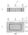
図1(a)及び(b)に示すように、実施形態のカーボンナノチューブシート1では、垂直方向に配向された複数のカーボンナノチューブ10aが横方向に微細な隙間を空けて並んで配列されている。 As shown in FIGS. 1 (a) and 1 (b), in the
複数のカーボンナノチューブ10aによってカーボンナノチューブ集合体10が形成される。図1(b)の平面図を参照すると、カーボンナノチューブ集合体10は四角状に形成されている。 A
カーボンナノチューブ集合体10の中央領域Aの隙間には熱可塑性樹脂部20が形成されている。熱可塑性樹脂部20は未硬化であってもよいし、あるいは硬化していてもよい。 A
熱可塑性樹脂部20の好適な一例としては、ヤング率が1.1GPa程度のポリエチレン樹脂、又はヤング率が1.1GPa程度のポリプロピレン樹脂が使用される。 As a suitable example of the
また、熱可塑性樹脂部20を取り囲むようにカーボンナノチューブ集合体10の外周領域Bの隙間に熱硬化性樹脂部22が形成されている。熱硬化性樹脂部22は未硬化の状態となっている。熱硬化性樹脂部22の好適な一例としては、ヤング率が2.4GPa程度のエポキシ樹脂、又はヤング率が2.8GPa程度のポリイミド樹脂が使用される。 In addition, a
このように、熱可塑性樹脂部20は、ヤング率が熱硬化性樹脂部22よりも小さい特性を有する。ヤング率が小さい方が柔軟性に優れ、ヤング率が大きい方が柔軟性が低く硬い特性を有する。 Thus, the
熱可塑性樹脂部20は熱硬化性樹脂部22よりも柔軟性が優れており、適度な弾力性をもっている。一方、熱硬化性樹脂部22は柔軟性が低いが高い接着力を有する。 The
後述するように、実施形態のカーボンナノチューブシート1は半導体素子の上面と放熱部材の下面との間に配置されて熱伝導性シートとして機能する。熱伝導性シートは、TIM(Thermal Interface Material)とも呼ばれる。 As will be described later, the
カーボンナノチューブシート1の中央領域Aに適度な柔軟性を有する熱可塑性樹脂部20を配置することにより、半導体素子の動作時の発熱による反りなどを十分に吸収できるようになっている。 By disposing the
さらに、カーボンナノチューブシート1の外周領域Bに接着強度の強い熱硬化性樹脂部22を配置することにより、カーボンナノチューブシート1の外周領域Bを半導体素子及び放熱部材に強固に接着することができる。 Furthermore, by disposing the
熱可塑性樹脂部20及び熱硬化性樹脂部22は各カーボンナノチューブ10aの上端を被覆している。一方、各カーボンナノチューブ10aの下端は熱可塑性樹脂部20及び熱硬化性樹脂部22から露出している。 The
カーボンナノチューブ10aの熱伝導率は1500W/mK〜3000W/mK程度であり、インジウムの熱伝導率(81W/mK程度)よりもかなり高い。しかも、カーボンナノチューブ10aはインジウムよりも機械的強度がかなり優れている。 The thermal conductivity of the
このため、カーボンナノチューブシート1は半導体素子からの発熱を放熱部材に伝導するための熱伝導性シートとして好適に使用することができる。 For this reason, the
上記したように、実施形態のカーボンナノチューブシート1は半導体素子と放熱部材との間に配置されて熱伝導性シートとして機能する。このとき、熱可塑性樹脂部20及び熱硬化性樹脂部22は熱伝導率が低いため、各カーボンナノチューブ10aの上端を被覆する熱可塑性樹脂部20及び熱硬化性樹脂部22は放熱部材で押圧されて横方向に押し出される。 As described above, the
これにより、各カーボンナノチューブ10aの上端が放熱部材の下面に接触するようになっている。 Thereby, the upper end of each
このような理由から、熱硬化性樹脂部22は未硬化の状態となっている。また、熱可塑性樹脂部20は、硬化した後でも再度加熱すると流動化するため、硬化状態であってもよいし、未硬化の状態であってもよい。 For this reason, the
あるいは、図2(a)及び(b)のカーボンナノチューブシート1aのように、各カーボンナノチューブ10aの上端が熱可塑性樹脂部20及び熱硬化性樹脂部22の上面から露出していてもよい。この場合は、上記した図1(a)及び(b)のカーボンナノチューブシート1の上面側の熱可塑性樹脂部20及び熱硬化性樹脂部22が機械研磨によって各カーボンナノチューブ10aの上端が露出するまで研磨される。その他の構成は図1(a)及び(b)のカーボンナノチューブシート1と同じである。 Or the upper end of each
図2(a)及び(b)のカーボンナノチューブシート1aを熱伝導性シートとして使用する際には、そのままの状態で各カーボンナノチューブ10aの上端の露出面が放熱部材に接触する。 When the
図2(a)及び(b)のカーボンナノチューブシート1aは、機械研磨を行う工程が必要となるため、図1(a)及び(b)のカーボンナノチューブシート1より製造コストの面で不利になる。 The
次に、図1(a)及び(b)のカーボンナノチューブシート1の製造方法について説明する。 Next, a method for producing the
図3(a)に示すように、まず、シリコン基板30を用意する。シリコン基板30は、カーボンナノチューブを形成するための土台として使用される。シリコン基板30の両面にシリコン酸化膜が形成されていてもよい。シリコン基板30上には複数のカーボンナノチューブ形成領域が画定されており、図3(a)では一つのカーボンナノチューブ形成領域が示されている。 As shown in FIG. 3A, first, a
基板としてシリコン基板30を例示するが、セラミックス基板又はガラス基板などの各種の基板を使用することができる。 Although the
次いで、図3(b)に示すように、シリコン基板30上の全面に、スパッタ法などにより膜厚が2.5nm程度の鉄(Fe)膜を形成して触媒金属膜32とする。触媒金属膜32は、CVD法によってカーボンナノチューブを形成するための触媒として形成される。 Next, as shown in FIG. 3B, an iron (Fe) film having a film thickness of about 2.5 nm is formed on the entire surface of the
触媒金属膜32としては、鉄以外に、コバルト(Co)、ニッケル(Ni)、金(Au)、銀(Ag)、又は白金(Pt)を使用してもよい。 As the
次いで、図3(c)に示すように、シリコン基板30を650℃の温度で5分〜10分間、加熱処理する。これにより、触媒金属膜32が微粒子化されて触媒金属微粒子32aが得られる。 Next, as shown in FIG. 3C, the
続いて、図3(d)に示すように、熱CVD(Chemical Vapor Deposition)法により、触媒金属微粒子32aを触媒としてシリコン基板30の上に複数のカーボンナノチューブ10aを成長させる。これにより、複数のカーボンナノチューブ10aが横方向に並んで形成されたカーボンナノチューブ集合体10が得られる。 Subsequently, as shown in FIG. 3D, a plurality of
図3(d)の部分拡大図に示すように、触媒金属微粒子32aに成長する各カーボンナノチューブ10aは、シリコン基板30の表面に対して垂直方向に配向して形成される。 As shown in the partially enlarged view of FIG. 3D, the
熱CVD法によるカーボンナノチューブ10aの成長条件としては、例えば、原料ガスとして分圧比が1:9のアセチレン・アルゴンガスの混合ガスが使用され、成膜チャンバの総ガス圧が1kPa、温度が650℃、成長時間が30分に設定される。 As a growth condition of the
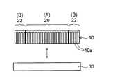
次いで、図4(a)に示すように、中央部に開口部22xが設けられた熱硬化性樹脂シート22aを用意する。熱硬化性樹脂シート22aは未硬化状態(Bステージ)の樹脂である。熱硬化性樹脂シート22aは、熱硬化性樹脂材の一例であり、前述した図1(a)及び(b)のカーボンナノチューブシート1の熱硬化性樹脂部22を形成するための樹脂材料である。 Next, as shown in FIG. 4A, a
また、図4(b)に示すように、熱硬化性樹脂シート22aの開口部22xの大きさに対応するサイズの未硬化の熱可塑性樹脂シート20aを用意する。熱可塑性樹脂シート20aは、熱可塑性樹脂材の一例であり、前述した図1(a)及び(b)のカーボンナノチューブシート1の熱可塑性樹脂部20を形成するための樹脂材料である。Moreover, as shown in FIG.4 (b), the uncured
その後に、図5(a)及び(b)に示すように、図4(a)の熱硬化性樹脂シート22aをカーボンナノチューブ集合体10の外周領域Bの上に配置する。さらに、図4(b)の熱可塑性樹脂シート20aを熱硬化性樹脂シート22aの開口部22x内に配置する。これにより、カーボンナノチューブ集合体10上の中央領域Aに配置された熱可塑性樹脂シート20aを取り囲むように熱硬化性樹脂シート22aが外周領域Bに配置される。 Thereafter, as shown in FIGS. 5A and 5B, the
次いで、押圧部材(不図示)で熱可塑性樹脂シート20a及び熱硬化性樹脂シート22aを下側に押圧しながら、温度:200℃、処理時間:1分の条件で加熱処理を行う。 Next, heat treatment is performed under the conditions of a temperature of 200 ° C. and a treatment time of 1 minute while pressing the
これにより、図6(a)及び(b)に示すように、カーボンナノチューブ集合体10の上に配置した熱可塑性樹脂シート20a及び熱硬化性樹脂シート22aを軟化させ、カーボンナノチューブ集合体10内の隙間に各樹脂を流し込んで含侵させる。 As a result, as shown in FIGS. 6A and 6B, the
このようにして、カーボンナノチューブ集合体10の中央領域Aの隙間に熱可塑性樹脂部20が含浸され、外周領域Bの隙間に熱硬化性樹脂部22が含浸される。 In this way, the
上記した樹脂の加熱条件を採用すると、この時点では、熱可塑性樹脂部20及び熱硬化性樹脂部22はまだ未硬化の状態となっている。 When the above-described resin heating conditions are employed, at this point, the
以上により、カーボンナノチューブ集合体10が熱可塑性樹脂部20及び熱硬化性樹脂部22で一体化されてシート状になる。 As described above, the
上記した形態では、熱可塑性樹脂シート20a及び熱硬化性樹脂シート22aを加熱して、熱可塑性樹脂部20及び熱硬化性樹脂部22を同時に形成している。この他に、熱可塑性樹脂部20を形成した後に、熱硬化性樹脂部22を形成してもよい。また逆に、熱硬化性樹脂部22を形成した後に、熱可塑性樹脂部20を形成してもよい。 In the above-described form, the
あるいは、液状の熱可塑性樹脂及び熱硬化性樹脂をディスペンサなどで塗り分けて熱可塑性樹脂部20及び熱硬化性樹脂部22を形成してもよい。 Alternatively, the
その後に、図7に示すように、シート状に一体化されたカーボンナノチューブ集合体10をシリコン基板30から引き剥がす。その後に、シート状に一体化されたカーボンナノチューブ集合体10を個々のカーボンナノチューブ形成領域が得られるように切断する。 Thereafter, as shown in FIG. 7, the
以上により、前述した図1(a)及び(b)のカーボンナノチューブシート1が製造される。カーボンナノチューブシート1は、カーボンナノチューブ集合体10を樹脂で一体化して一枚のシート状にしているため、良好なハンドリング性を有する。 Thus, the
前述した図2(a)及び(b)のカーボンナノチューブシート1aを採用する場合は、図8に示すように、前述した図6(a)の工程の後に、カーボンナノチューブ集合体10の上面側の熱可塑性樹脂部20及び熱硬化性樹脂部22を機械研磨などで除去する。これにより、各カーボンナノチューブ10aの上端を熱可塑性樹脂部20及び熱硬化性樹脂部22から露出させる。 When the
次に、図1(a)及び(b)のカーボンナノチューブシート1を熱伝導性シートとして使用する半導体装置に製造方法について説明する。 Next, a manufacturing method for a semiconductor device that uses the
図9(a)に示すように、まず、配線基板40を用意する。配線基板40は、上面側に銅などからなる接続パッドPを備え、下面側にはんだなどからなる外部接続端子Tを備えている。接続パッドPは、配線基板40の内部に形成された多層配線(不図示)を介して外部接続端子Tに電気的に接続されている。 As shown in FIG. 9A, first, a
次いで、図9(b)に示すように、下面側にバンプ電極52を備えた半導体素子50(LSIチップ)を用意する。そして、半導体素子50のバンプ電極52をはんだ(不図示)を介して配線基板40の接続パッドPにフリップチップ接続する。半導体素子50としては、動作時に発熱量が大きなCPUチップなどが使用される。 Next, as shown in FIG. 9B, a semiconductor element 50 (LSI chip) having a
その後に、半導体素子50と配線基板40との隙間にアンダーフィル樹脂54を充填する。 Thereafter, an
次いで、図9(c)に示すように、前述した図1(a)及び(b)のカーボンナノチューブシート1を半導体素子50の上面に配置する。カーボンナノチューブシート1は、熱可塑性樹脂部20及び熱硬化性樹脂部22が各カーボンナノチューブ10aを被覆している面側が上側になるように、半導体素子50の上面に配置される。 Next, as shown in FIG. 9C, the above-described
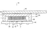
続いて、図10に示すように、放熱部材としてヒートスプレッダ60を用意する。ヒートスプレッダ60は、平板部62と、その周縁から下側に突き出る環状の突出部64とを備えており、下面側の中央部に凹部Cが設けられている。ヒートスプレッダ60の一例としては、無酸素銅部材の外面にニッケルめっきを施したものが使用される。 Then, as shown in FIG. 10, the
次いで、図11に示すように、ヒートスプレッダ60の突出部64を熱硬化性の接着剤66を介して配線基板40の周縁部に配置する。 Next, as shown in FIG. 11, the protruding
さらに、押圧部材(不図示)でヒートスプレッダ60を下側に押圧しながら、温度:250℃、処理時間:20〜30分の条件で加熱処理を行う。 Further, heat treatment is performed under the conditions of temperature: 250 ° C. and treatment time: 20 to 30 minutes while pressing the
このとき、ヒートスプレッダ60の凹部Cの底面がカーボンナノチューブシート1の各カーボンナノチューブ10aの上端に当接するように、ヒートスプレッダ60の凹部Cの深さが調節されている。 At this time, the depth of the concave portion C of the
これにより、図11の部分拡大図に示すように、カーボンナノチューブシート1の上側の熱可塑性樹脂部20及び未硬化の熱硬化性樹脂部22が流動して横方向に押し出される。熱可塑性樹脂部20は、硬化している場合であっても再加熱により軟化して横方向に押し出される。 Thereby, as shown in the partially enlarged view of FIG. 11, the
これにより、カーボンナノチューブシート1の各カーボンナノチューブ10aの上端がヒートスプレッダ60の凹部Cの底面に接触した状態となる。カーボンナノチューブシート1の各カーボンナノチューブ10aの下端は元々露出しているため、半導体素子50の上面に接触した状態となる。 As a result, the upper ends of the
この加熱処理により、カーボンナノチューブシート1の熱可塑性樹脂部20及び熱硬化性樹脂部22が完全に硬化する。 By this heat treatment, the
これにより、カーボンナノチューブシート1の上面とヒートスプレッダ60の凹部Cの底面とが熱可塑性樹脂部20及び熱硬化性樹脂部22によって接着される。また同時に、カーボンナノチューブシート1の下面と半導体素子50の上面とが熱可塑性樹脂部20及び熱硬化性樹脂部22によって接着される。さらに同時に、ヒートスプレッダ60の突出部64が配線基板40の周縁部に熱硬化性の接着剤66によって接着される。 Thereby, the upper surface of the
以上により、実施形態の半導体装置2が製造される。 Thus, the
なお、カーボンナノチューブシート1の上面側をヒートスプレッダ60の凹部Cの底面に押圧して接着した後に、カーボンナノチューブシート1の下面側を半導体素子50の上面に接着してもよい。 Note that the lower surface side of the
図11に示すように、実施形態の半導体装置2は、前述した図9(a)で説明した配線基板40の接続パッドPに半導体素子50のバンプ電極52がフリップチップ接続されている。半導体素子50と配線基板40の間にアンダーフィル樹脂54が充填されている。 As shown in FIG. 11, in the
また、配線基板40の周縁部にはヒートスプレッダ60の環状の突出部64が接着剤66よって接着されている。これにより、ヒートスプレッダ60の凹部C内に半導体素子50が収容されている。 An
半導体素子50の上面とヒートスプレッダ60の凹部Cの底面との間の領域に、熱伝導性シートとして図1(a)のカーボンナノチューブシート1が設けられている。カーボンナノチューブシート1の外周領域Bの下面は熱硬化性樹脂部22によって半導体素子50の上面に接着されている。また、カーボンナノチューブシート1の外周領域Bの上面は熱硬化性樹脂部22によってヒートスプレッダ60の凹部Cの底面に接着されている。 In the region between the upper surface of the
また、カーボンナノチューブシート1の中央領域Aの下面は熱可塑性樹脂部20によって半導体素子50の上面に接着されている。また、カーボンナノチューブシート1の中央領域Aの上面は熱可塑性樹脂部20によってヒートスプレッダ60の凹部Cの底面に接着されている。 Further, the lower surface of the central region A of the
そして、カーボンナノチューブシート1の各カーボンナノチューブ10aの下端が半導体素子50の上面に接触している。また、カーボンナノチューブシート1の各カーボンナノチューブ10aの上端がヒートスプレッダ60の凹部Cの底面に接触している。 The lower end of each
このように、実施形態の半導体装置2では、前述した製造方法で説明したように、熱伝導度が高いカーボンナノチューブ10aの上端及び下端をヒートスプレッダ60及び半導体素子50に確実に接触させることができる。 Thus, in the
これにより、熱伝導経路の熱抵抗が小さくなり、半導体素子50から発する熱を、カーボンナノチューブシート1を介してヒートスプレッダ60側に十分に伝導して放熱することができる。 Thereby, the thermal resistance of the heat conduction path is reduced, and the heat generated from the
また、カーボンナノチューブシート1の中央領域Aには、適度な柔軟性を有する熱可塑性樹脂部20が形成されている。このため、半導体素子50の動作中の発熱によって反りが発生しも、反りを熱可塑性樹脂部20で吸収することができる。 Further, a
よって、半導体素子50の動作中に反りが発生しても、各カーボンナノチューブ10aの上端及び下端が常にヒートスプレッダ60及び半導素子50に接触することができる。このため、半導体装置2内の熱伝導経路の接触熱抵抗の変化を抑えることができるので、安定して高い放熱性能を得ることができる。これにより、発熱量が多いCPUチップなどの半導体素子50を正常に動作させることができる。 Therefore, even if warpage occurs during the operation of the
また、半導体素子のマルチチップ化により複数の半導体素子の間で段差が生じる場合であっても、柔軟性を有する熱可塑性樹脂部20によって段差を吸収することができる。 Further, even when a step is generated between a plurality of semiconductor elements due to the multi-chip semiconductor element, the step can be absorbed by the
また、カーボンナノチューブシート1の外周領域Bには、柔軟性や流動性は乏しいが接着強度が高い熱硬化性樹脂部22が形成されている。これにより、カーボンナノチューブシート1を半導体素子50及びヒートスプレッダ60に強固に接着することができる。 Further, in the outer peripheral region B of the
よって、半導体素子50の動作中に反りが発生しても、カーボンナノチューブシート1と、半導体素子50及びヒートスプレッダ60との接着が保持され、カーボンナノチューブシート1の剥離が防止される。 Therefore, even if warpage occurs during the operation of the
また、外周領域Bの熱硬化性樹脂部22は中央領域Aの熱可塑性樹脂部20よりも樹脂の剛性が高いため、カーボンナノチューブシート1の圧縮変形を防止することができる。 In addition, since the
さらには、外周領域Bの熱硬化性樹脂部22内にもカーボンナノチューブ10aが存在するため、外周領域Bでの熱伝導性も高く、半導体素子50の熱を効率よくヒートスプレッダ60に伝導させることができる。 Furthermore, since the
このように、実施形態のカーボンナノチューブシート1は、中央領域Aで適度な柔軟性を有し、外周領域Bで強い接着性を併せもつため、半導体素子50に反りが発生しても剥離することなく安定して熱を伝導することができる。 Thus, since the
ここで、本実施形態と違って、全体にわたって熱硬化性樹脂を含浸させて硬化させたカーボンナノチューブシートを使用する場合について言及する。この場合は、硬化した熱硬化性樹脂は再加熱しても流動化しないため、前述した図11の工程で、カーボンナノチューブ10aの上端を露出させてヒートスプレッダ60に接触させることは困難である。 Here, unlike the present embodiment, the case of using a carbon nanotube sheet that has been impregnated and cured with a thermosetting resin throughout will be described. In this case, since the cured thermosetting resin does not flow even when reheated, it is difficult to expose the upper end of the
これに対して、熱可塑性樹脂は硬化した後も再加熱で流動化するため、プロセスが制限されることなく主要部のカーボンナノチューブ10aの上端を容易に露出させることができるという観点からも有利である。 On the other hand, since the thermoplastic resin is fluidized by reheating after curing, it is advantageous from the viewpoint that the upper end of the
図12に示す半導体装置2aでは、図11の半導体装置2のヒートスプレッダ60の上に熱伝導材68を介してヒートシンク70がさらに設けられている。ヒートシンク70は平板部72とその上に突き出る多数の放熱フィン74とから形成される。熱伝導材68として、前述した実施形態のカーボンナノチューブシート1を使用してもよい。 In the
図12の半導体装置2aのヒートスプレッダ60及びヒートシンク70が放熱部材の一例である。 The
さらに、図13に示す半導体装置2bでは、図11の半導体装置2のヒートスプレッダ60の上に熱伝導材68を介してヒートパイプ80がさらに設けられている。ヒートパイプ80では、密閉したパイプ内に封入された作動液体の蒸発・凝縮の相変化で熱を輸送して放熱する。 Further, in the
図13の半導体装置2bにおいても、熱伝導材68として、前述した実施形態のカーボンナノチューブシート1を使用してもよい。 Also in the
図13の半導体装置2bのヒートスプレッダ60及びヒートパイプ80が放熱部材の一例である。 The
(その他の実施形態)
前述した図1(a)及び(b)のカーボンナノチューブシート1では、カーボンナノチューブ集合体10の中央領域Aの全体に一括して熱可塑性樹脂部20を形成している。(Other embodiments)
In the
図14に示すカーボンナノチューブシート1bでは、熱可塑性樹脂部20がカーボンナノチューブ集合体10の中央領域Aに複数個に分割されて配置されている。そして、熱硬化性樹脂部22は、カーボンナノチューブ集合体10の外周領域Bから中央領域Aに延びて形成され、複数の熱可塑性樹脂部20を取り囲んで形成される。In the
半導体素子の発熱しやすい部位に合わせて複数の熱可塑性樹脂部20を分割して配置することにより、半導体素子からの熱を効率よく外部に伝導することができる。また、カーボンナノチューブシート1bの中央領域Aの一部にも接着性の強い熱硬化性樹脂部22が形成されるため、接着強度を強くする際に都合がよい。 By dividing and arranging the plurality of
複数の熱可塑性樹脂部20は、円形以外に四角形などの各種の形状を採用できると共に、分割数も任意に設定することができる。 The plurality of
図14のカーボンナノチューブシート1bを製造するには、前述した図5(a)及び(b)の工程で、カーボンナノチューブ集合体10の上に複数の開口部が設けられた熱硬化性樹脂材を配置し、その開口部に熱可塑性樹脂材をそれぞれ配置して、同様に樹脂を含浸させればよい。In order to manufacture the
また、図15(a)及び(b)に示すカーボンナノチューブシート1cのように、中央領域Aの熱可塑性樹脂部20内のみにカーボンナノチューブ10aが設けられ、外周領域Bの熱硬化性樹脂部22の中にカーボンナノチューブ10aが存在しない構造としてもよい。Further, like the
この場合は、カーボンナノチューブシート1cは、外周領域Bの全体に配置された熱硬化性樹脂部22によって半導体素子及びヒートスプレッダにより強固に接着される。この形態では、熱硬化性樹脂部22の中にカーボンナノチューブが存在しないため、図1(a)及び(b)のカーボンナノチューブシート1よりも放熱性の面で不利になる。 In this case, the
1,1a,1b、1c…カーボンナノチューブシート、2,2a,2b…半導体装置、10…カーボンナノチューブ集合体、10a…カーボンナノチューブ、20…熱可塑性樹脂部、20a…熱可塑性樹脂シート、22…熱硬化性樹脂部、22a…熱硬化性樹脂シート、22x…開口部、30…シリコン基板、32…触媒金属膜、32a…触媒金属微粒子、40…配線基板、50…半導体素子、52…バンプ電極、54…アンダーフィル樹脂、60…ヒートスプレッダ、62…平板部、64…突出部、70…ヒートシンク、72…平板部、74…放熱フィン、80…ヒートパイプ、A…中央領域、B…外周領域、P…接続パッド、T…外部接続端子。DESCRIPTION OF
Claims (10)
Translated fromJapanese前記カーボンナノチューブ集合体の中央領域に形成された熱可塑性樹脂部と、
前記熱可塑性樹脂部を取り囲むように前記カーボンナノチューブ集合体の外周領域に形成された未硬化の熱硬化性樹脂部と
を有し、
前記熱可塑性樹脂部と前記熱硬化性樹脂部とは、前記カーボンナノチューブの下端から上端に形成され、
前記熱可塑性樹脂部の側面と前記熱硬化性樹脂部の側面とが前記カーボンナノチューブの間の領域で接していることを特徴とするカーボンナノチューブシート。An aggregate of carbon nanotubes in which a plurality of carbon nanotubes are arranged;
A thermoplastic resin portion formed in a central region of the carbon nanotube aggregate;
An uncured thermosetting resin portion formed in an outer peripheral region of the carbon nanotube aggregate so as to surround the thermoplastic resin portion,
The thermoplastic resin portion and the thermosetting resin portion are formed from the lower end to the upper end of the carbon nanotube,
A carbon nanotube sheet, wherein a side surface of the thermoplastic resin portion and a side surface of the thermosetting resin portion are in contact with each other in a region between the carbon nanotubes.
前記配線基板の接続パッドに接続された半導体素子と、
前記半導体素子の上に配置され、複数のカーボンナノチューブが配列されたカーボンナノチューブ集合体と、前記カーボンナノチューブ集合体の中央領域に形成された熱可塑性樹脂部と、前記熱可塑性樹脂部を取り囲むように前記カーボンナノチューブ集合体の外周領域に形成された熱硬化性樹脂部とを含み、
前記熱可塑性樹脂部と前記熱硬化性樹脂部とは、前記カーボンナノチューブの下端から上端に形成され、前記熱可塑性樹脂部の側面と前記熱硬化性樹脂部の側面とが前記カーボンナノチューブの間の領域で接しているカーボンナノチューブシートと、
前記カーボンナノチューブシートの上に配置された放熱部材と
を有することを特徴とする半導体装置。A wiring board;
A semiconductor element connected to a connection pad of the wiring board;
A carbon nanotube aggregate arranged on the semiconductor element and arranged with a plurality of carbon nanotubes, a thermoplastic resin portion formed in a central region of the carbon nanotube aggregate, and surrounding the thermoplastic resin portion A thermosetting resin portion formed in the outer peripheral region of the carbon nanotube aggregate,
The thermoplastic resin portion and the thermosetting resin portion are formed from the lower end to the upper end of the carbon nanotube, and the side surface of the thermoplastic resin portion and the side surface of the thermosetting resin portion are between the carbon nanotubes. A carbon nanotube sheet in contact with the region;
And a heat dissipating member disposed on the carbon nanotube sheet.
前記カーボンナノチューブ集合体上の中央領域に熱可塑性樹脂材を配置すると共に、前記熱可塑性樹脂材を取り囲むように前記カーボンナノチューブ集合体上の外周領域に未硬化の熱硬化性樹脂材を配置する工程と、
加熱処理することにより、前記熱可塑性樹脂材及び前記熱硬化性樹脂材を流動させて前記カーボンナノチューブ集合体の隙間に含浸させる工程と、
前記基板を除去する工程と
を有し、
前記熱可塑性樹脂材と前記熱硬化性樹脂材とは、前記カーボンナノチューブの下端から上端に形成され、前記熱可塑性樹脂材の側面と前記熱硬化性樹脂材の側面とが前記カーボンナノチューブの間の領域で接することを特徴とするカーボンナノチューブシートの製造方法。Forming a plurality of carbon nanotubes on a substrate to obtain a carbon nanotube aggregate;
Disposing a thermoplastic resin material in a central region on the carbon nanotube aggregate and disposing an uncured thermosetting resin material in an outer peripheral region on the carbon nanotube aggregate so as to surround the thermoplastic resin material When,
A step of allowing the thermoplastic resin material and the thermosetting resin material to flow and impregnating the gaps of the carbon nanotube aggregates by heat treatment;
And removing the substrate.
The thermoplastic resinmaterial and the thermosetting resinmaterial are formed from the lower end to the upper end of the carbon nanotube, and the sidesurface of the thermoplastic resinmaterial and the sidesurface of the thermosetting resinmaterial are between the carbon nanotubes. A method for producing a carbon nanotube sheet, wherein the carbon nanotube sheet is contacted in a region.
前記カーボンナノチューブ集合体の上端が前記熱硬化性樹脂材及び前記熱可塑性樹脂材で被覆され、かつ前記熱硬化性樹脂材は未硬化の状態で含浸されることを特徴とする請求項6に記載のカーボンナノチューブシートの製造方法。In the step of impregnating the thermosetting resin material and the thermoplastic resin material,
The upper end of the carbon nanotube aggregate is covered with the thermosetting resin material and the thermoplastic resin material, and the thermosetting resin material is impregnated in an uncured state. Of manufacturing the carbon nanotube sheet.
前記カーボンナノチューブ集合体の上端を被覆する前記熱可塑性樹脂材及び前記熱硬化性樹脂材を研磨して、前記カーボンナノチューブの上端を露出させる工程を有することを特徴とする請求項7に記載のカーボンナノチューブシートの製造方法。After the step of impregnating the thermoplastic resin material and the thermosetting resin material,
The carbon according to claim 7, further comprising a step of polishing the thermoplastic resin material and the thermosetting resin material covering the upper end of the carbon nanotube aggregate to expose the upper end of the carbon nanotube. Manufacturing method of nanotube sheet.
複数のカーボンナノチューブが配列されたカーボンナノチューブ集合体と、前記カーボンナノチューブ集合体の中央領域に含浸された熱可塑性樹脂部と、前記熱可塑性樹脂部を取り囲むように前記カーボンナノチューブ集合体の外周領域に含浸された未硬化の熱硬化性樹脂部とを含み、
前記熱可塑性樹脂部と前記熱硬化性樹脂部とは、前記カーボンナノチューブの下端から上端に形成され、前記熱可塑性樹脂部の側面と前記熱硬化性樹脂部の側面とが前記カーボンナノチューブの間の領域で接し、かつ、
前記カーボンナノチューブ集合体の上端が前記熱硬化性樹脂部及び前記熱可塑性樹脂部で被覆されたカーボンナノチューブシートを用意する工程と、
前記カーボンナノチューブシートを前記半導体素子の上に配置する工程と、
前記カーボンナノチューブシートの上に放熱部材を配置し、前記放熱部材を下側に押圧しながら加熱処理することにより、前記カーボンナノチューブ集合体上の前記熱可塑性樹脂部及び前記熱硬化性樹脂部を横方向に押し出して、前記カーボンナノチューブ集合体の上端を前記放熱部材に接触させる工程と
を有することを特徴とする半導体装置の製造方法。Connecting the semiconductor element to the connection pad of the wiring board;
A carbon nanotube aggregate in which a plurality of carbon nanotubes are arranged, a thermoplastic resin portion impregnated in a central region of the carbon nanotube aggregate, and an outer peripheral region of the carbon nanotube aggregate so as to surround the thermoplastic resin portion And impregnated uncured thermosetting resin part,
The thermoplastic resin portion and the thermosetting resin portion are formed from the lower end to the upper end of the carbon nanotube, and the side surface of the thermoplastic resin portion and the side surface of the thermosetting resin portion are between the carbon nanotubes. Touch in the area, and
Preparing a carbon nanotube sheet in which an upper end of the carbon nanotube aggregate is coated with the thermosetting resin portion and the thermoplastic resin portion;
Disposing the carbon nanotube sheet on the semiconductor element;
A heat dissipating member is disposed on the carbon nanotube sheet, and the thermoplastic resin portion and the thermosetting resin portion on the carbon nanotube aggregate are horizontally disposed by performing heat treatment while pressing the heat dissipating member downward. And a step of bringing the carbon nanotube aggregate into contact with the heat radiating member by extruding the carbon nanotube aggregate in a direction.
前記放熱部材は、下面側に凹部を備えて周縁に突出部が設けられており、前記放熱部材の突出部が前記配線基板に接着され、前記放熱部材の凹部の底面に前記カーボンナノチューブシートの上面が接触することを特徴とする請求項9に記載の半導体装置の製造方法。In the step of bringing the upper end of the carbon nanotube into contact with the heat radiating member,
The heat dissipating member has a recess on the lower surface side, and a protrusion is provided on the periphery. The protrusion of the heat dissipating member is bonded to the wiring board, and the upper surface of the carbon nanotube sheet is formed on the bottom surface of the recess of the heat dissipating member. The method of manufacturing a semiconductor device according to claim 9, wherein:
Priority Applications (3)
| Application Number | Priority Date | Filing Date | Title |
|---|---|---|---|
| JP2014010306AJP6261352B2 (en) | 2014-01-23 | 2014-01-23 | Carbon nanotube sheet, semiconductor device, method of manufacturing carbon nanotube sheet, and method of manufacturing semiconductor device |
| US14/533,556US9873825B2 (en) | 2014-01-23 | 2014-11-05 | Carbon nanotube sheet, semiconductor device, method of manufacturing carbon nanotube sheet, and method of manufacturing semiconductor device |
| CN201410643282.7ACN104810335B (en) | 2014-01-23 | 2014-11-06 | The manufacturing method of carbon nanotube pieces and semiconductor device, the manufacturing method of carbon nanotube pieces and semiconductor device |
Applications Claiming Priority (1)
| Application Number | Priority Date | Filing Date | Title |
|---|---|---|---|
| JP2014010306AJP6261352B2 (en) | 2014-01-23 | 2014-01-23 | Carbon nanotube sheet, semiconductor device, method of manufacturing carbon nanotube sheet, and method of manufacturing semiconductor device |
Publications (3)
| Publication Number | Publication Date |
|---|---|
| JP2015138903A JP2015138903A (en) | 2015-07-30 |
| JP2015138903A5 JP2015138903A5 (en) | 2016-10-27 |
| JP6261352B2true JP6261352B2 (en) | 2018-01-17 |
Family
ID=53545463
Family Applications (1)
| Application Number | Title | Priority Date | Filing Date |
|---|---|---|---|
| JP2014010306AActiveJP6261352B2 (en) | 2014-01-23 | 2014-01-23 | Carbon nanotube sheet, semiconductor device, method of manufacturing carbon nanotube sheet, and method of manufacturing semiconductor device |
Country Status (3)
| Country | Link |
|---|---|
| US (1) | US9873825B2 (en) |
| JP (1) | JP6261352B2 (en) |
| CN (1) | CN104810335B (en) |
Families Citing this family (8)
| Publication number | Priority date | Publication date | Assignee | Title |
|---|---|---|---|---|
| KR20190021230A (en)* | 2016-06-28 | 2019-03-05 | 니폰 제온 가부시키가이샤 | Heat sink |
| KR102546241B1 (en)* | 2016-10-05 | 2023-06-22 | 삼성전자주식회사 | Semiconductor package |
| US10861763B2 (en) | 2016-11-26 | 2020-12-08 | Texas Instruments Incorporated | Thermal routing trench by additive processing |
| US11004680B2 (en)* | 2016-11-26 | 2021-05-11 | Texas Instruments Incorporated | Semiconductor device package thermal conduit |
| WO2018156878A1 (en)* | 2017-02-24 | 2018-08-30 | Lintec Of America, Inc. | Nanofiber thermal interface material |
| CN112602189A (en)* | 2018-08-23 | 2021-04-02 | 昭和电工材料株式会社 | Method for manufacturing semiconductor device, thermally conductive sheet, and method for manufacturing thermally conductive sheet |
| JP7338738B2 (en)* | 2018-08-23 | 2023-09-05 | 株式会社レゾナック | Method for manufacturing semiconductor device, heat conductive sheet, and method for manufacturing heat conductive sheet |
| US11915991B2 (en)* | 2021-03-26 | 2024-02-27 | Taiwan Semiconductor Manufacturing Company, Ltd. | Semiconductor device having first heat spreader and second heat spreader and manufacturing method thereof |
Family Cites Families (14)
| Publication number | Priority date | Publication date | Assignee | Title |
|---|---|---|---|---|
| CN100383213C (en)* | 2004-04-02 | 2008-04-23 | 清华大学 | A kind of thermal interface material and its manufacturing method |
| US7135769B2 (en)* | 2005-03-29 | 2006-11-14 | Taiwan Semiconductor Manufacturing Company, Ltd. | Semiconductor packages and methods of manufacturing thereof |
| CN101054467B (en)* | 2006-04-14 | 2010-05-26 | 清华大学 | Carbon nanotube composite material and preparation method thereof |
| US7489033B2 (en)* | 2006-11-10 | 2009-02-10 | Intel Corporation | Electronic assembly with hot spot cooling |
| WO2008103221A1 (en)* | 2007-02-22 | 2008-08-28 | Dow Corning Corporation | Process for preparing conductive films and articles prepared using the process |
| JP5104688B2 (en)* | 2007-10-22 | 2012-12-19 | 富士通株式会社 | Sheet-like structure, method for producing the same, and electronic device |
| JP5276565B2 (en)* | 2009-10-14 | 2013-08-28 | 新光電気工業株式会社 | Heat dissipation parts |
| JP5295932B2 (en) | 2009-11-02 | 2013-09-18 | 新光電気工業株式会社 | Semiconductor package, evaluation method thereof, and manufacturing method thereof |
| JP5842349B2 (en)* | 2011-03-18 | 2016-01-13 | 富士通株式会社 | Sheet-like structure, method for producing sheet-like structure, electronic device, and method for producing electronic device |
| JP5673325B2 (en) | 2011-04-20 | 2015-02-18 | 富士通株式会社 | Carbon nanotube formation method and thermal diffusion apparatus |
| JP6015009B2 (en)* | 2012-01-25 | 2016-10-26 | 富士通株式会社 | Electronic device and manufacturing method thereof |
| KR101332866B1 (en)* | 2012-02-16 | 2013-11-22 | 앰코 테크놀로지 코리아 주식회사 | Semiconductor package and method for manufacturing the same |
| JP5928181B2 (en)* | 2012-06-18 | 2016-06-01 | 富士通株式会社 | Electronic device manufacturing method and electronic device |
| US9041192B2 (en)* | 2012-08-29 | 2015-05-26 | Broadcom Corporation | Hybrid thermal interface material for IC packages with integrated heat spreader |
- 2014
- 2014-01-23JPJP2014010306Apatent/JP6261352B2/enactiveActive
- 2014-11-05USUS14/533,556patent/US9873825B2/enactiveActive
- 2014-11-06CNCN201410643282.7Apatent/CN104810335B/enactiveActive
Also Published As
| Publication number | Publication date |
|---|---|
| CN104810335A (en) | 2015-07-29 |
| US20150206822A1 (en) | 2015-07-23 |
| CN104810335B (en) | 2018-11-13 |
| JP2015138903A (en) | 2015-07-30 |
| US9873825B2 (en) | 2018-01-23 |
Similar Documents
| Publication | Publication Date | Title |
|---|---|---|
| JP6261352B2 (en) | Carbon nanotube sheet, semiconductor device, method of manufacturing carbon nanotube sheet, and method of manufacturing semiconductor device | |
| JP5276565B2 (en) | Heat dissipation parts | |
| JP5733893B2 (en) | Electronic component equipment | |
| TWI663695B (en) | Chip package structure and manufacturing method thereof | |
| JP6283293B2 (en) | Method for producing carbon nanotube sheet | |
| CN101540302A (en) | Sheet structure and method of manufacturing sheet structure | |
| TWI242863B (en) | Heat dissipating structure and semiconductor package with the heat dissipating structure | |
| TW201640627A (en) | Electronic package structure and the manufacture thereof | |
| JP2014060252A (en) | Method of manufacturing heat dissipation material | |
| JP2002033411A (en) | Semiconductor device with heat spreader and its manufacturing method | |
| JP2016063178A (en) | Semiconductor device and manufacturing method of the same | |
| JP2011187877A (en) | Semiconductor device, and method of manufacturing the same | |
| CN102881667A (en) | Semiconductor Package Structure | |
| JP5343620B2 (en) | Heat dissipation material and method for manufacturing the same, electronic device and method for manufacturing the same | |
| CN108346630B (en) | Heat dissipation package structure | |
| TW201832297A (en) | Package on package structure and manufacturing method thereof | |
| TW201203500A (en) | Semiconductor package and manufacturing method thereof | |
| TWI721898B (en) | Semiconductor package structure | |
| US9644128B2 (en) | Carbon nanotube sheet, electronic device, method of manufacturing carbon nanotube sheet, and method of manufacturing electronic device | |
| CN209880589U (en) | Semiconductor packaging structure | |
| JP5808227B2 (en) | Heat dissipation component, semiconductor package and manufacturing method thereof | |
| JP2001217359A (en) | Radiator fin, manufacturing method thereof, and semiconductor device | |
| CN112117243A (en) | Semiconductor packaging structure and preparation method thereof | |
| TW202021068A (en) | Electronic package and manufacturing method thereof and cooling part | |
| CN112185908B (en) | Semiconductor packaging structure and preparation method thereof |
Legal Events
| Date | Code | Title | Description |
|---|---|---|---|
| A521 | Written amendment | Free format text:JAPANESE INTERMEDIATE CODE: A523 Effective date:20160909 | |
| A621 | Written request for application examination | Free format text:JAPANESE INTERMEDIATE CODE: A621 Effective date:20160909 | |
| A977 | Report on retrieval | Free format text:JAPANESE INTERMEDIATE CODE: A971007 Effective date:20170725 | |
| A131 | Notification of reasons for refusal | Free format text:JAPANESE INTERMEDIATE CODE: A131 Effective date:20170822 | |
| A521 | Written amendment | Free format text:JAPANESE INTERMEDIATE CODE: A523 Effective date:20171004 | |
| TRDD | Decision of grant or rejection written | ||
| A01 | Written decision to grant a patent or to grant a registration (utility model) | Free format text:JAPANESE INTERMEDIATE CODE: A01 Effective date:20171121 | |
| A61 | First payment of annual fees (during grant procedure) | Free format text:JAPANESE INTERMEDIATE CODE: A61 Effective date:20171212 | |
| R150 | Certificate of patent or registration of utility model | Ref document number:6261352 Country of ref document:JP Free format text:JAPANESE INTERMEDIATE CODE: R150 |