JP6254036B2 - Three-dimensional laminating apparatus and three-dimensional laminating method - Google Patents
Three-dimensional laminating apparatus and three-dimensional laminating methodDownload PDFInfo
- Publication number
- JP6254036B2 JP6254036B2JP2014074058AJP2014074058AJP6254036B2JP 6254036 B2JP6254036 B2JP 6254036B2JP 2014074058 AJP2014074058 AJP 2014074058AJP 2014074058 AJP2014074058 AJP 2014074058AJP 6254036 B2JP6254036 B2JP 6254036B2
- Authority
- JP
- Japan
- Prior art keywords
- unit
- powder
- heating
- dimensional
- light
- Prior art date
- Legal status (The legal status is an assumption and is not a legal conclusion. Google has not performed a legal analysis and makes no representation as to the accuracy of the status listed.)
- Active
Links
- 238000010030laminatingMethods0.000titleclaimsdescription119
- 238000000034methodMethods0.000titleclaimsdescription50
- 239000000843powderSubstances0.000claimsdescription248
- 238000010438heat treatmentMethods0.000claimsdescription169
- 238000000465mouldingMethods0.000claimsdescription153
- 239000000463materialSubstances0.000claimsdescription66
- 230000007246mechanismEffects0.000claimsdescription48
- 238000001514detection methodMethods0.000claimsdescription43
- 238000005259measurementMethods0.000claimsdescription35
- 239000004065semiconductorSubstances0.000claimsdescription32
- 238000003475laminationMethods0.000claimsdescription23
- 239000013307optical fiberSubstances0.000claimsdescription23
- 238000009826distributionMethods0.000claimsdescription16
- 230000001678irradiating effectEffects0.000claimsdescription16
- 239000000155meltSubstances0.000claimsdescription15
- 238000011144upstream manufacturingMethods0.000claimsdescription7
- 238000002844meltingMethods0.000claimsdescription5
- 230000008018meltingEffects0.000claimsdescription5
- 230000009467reductionEffects0.000claimsdescription2
- 238000007711solidificationMethods0.000claimsdescription2
- 230000008023solidificationEffects0.000claimsdescription2
- 235000013312flourNutrition0.000claims1
- 239000012254powdered materialSubstances0.000claims1
- 238000003754machiningMethods0.000description91
- 238000003860storageMethods0.000description58
- 239000007789gasSubstances0.000description36
- NJPPVKZQTLUDBO-UHFFFAOYSA-NnovaluronChemical compoundC1=C(Cl)C(OC(F)(F)C(OC(F)(F)F)F)=CC=C1NC(=O)NC(=O)C1=C(F)C=CC=C1FNJPPVKZQTLUDBO-UHFFFAOYSA-N0.000description34
- 238000010586diagramMethods0.000description33
- 238000004519manufacturing processMethods0.000description31
- 230000008569processEffects0.000description30
- 238000012545processingMethods0.000description25
- 238000011084recoveryMethods0.000description14
- 230000015572biosynthetic processEffects0.000description11
- 238000004891communicationMethods0.000description9
- 238000013461designMethods0.000description9
- XKRFYHLGVUSROY-UHFFFAOYSA-NArgonChemical compound[Ar]XKRFYHLGVUSROY-UHFFFAOYSA-N0.000description8
- QVGXLLKOCUKJST-UHFFFAOYSA-Natomic oxygenChemical compound[O]QVGXLLKOCUKJST-UHFFFAOYSA-N0.000description8
- 230000008859changeEffects0.000description8
- 239000001301oxygenSubstances0.000description8
- 229910052760oxygenInorganic materials0.000description8
- 238000007493shaping processMethods0.000description8
- 238000003384imaging methodMethods0.000description7
- 238000002156mixingMethods0.000description6
- 238000003756stirringMethods0.000description6
- 238000000105evaporative light scattering detectionMethods0.000description5
- 230000005484gravityEffects0.000description5
- 239000002245particleSubstances0.000description5
- IJGRMHOSHXDMSA-UHFFFAOYSA-NAtomic nitrogenChemical compoundN#NIJGRMHOSHXDMSA-UHFFFAOYSA-N0.000description4
- 229910052786argonInorganic materials0.000description4
- 239000011261inert gasSubstances0.000description4
- 239000002184metalSubstances0.000description4
- 229910052751metalInorganic materials0.000description4
- 230000003746surface roughnessEffects0.000description4
- 230000007423decreaseEffects0.000description3
- 230000002093peripheral effectEffects0.000description3
- 238000005507sprayingMethods0.000description3
- XEEYBQQBJWHFJM-UHFFFAOYSA-NIronChemical compound[Fe]XEEYBQQBJWHFJM-UHFFFAOYSA-N0.000description2
- 239000000470constituentSubstances0.000description2
- 238000007599dischargingMethods0.000description2
- 238000002347injectionMethods0.000description2
- 239000007924injectionSubstances0.000description2
- 239000007769metal materialSubstances0.000description2
- 229910052757nitrogenInorganic materials0.000description2
- 239000012255powdered metalSubstances0.000description2
- 239000002994raw materialSubstances0.000description2
- 239000007921spraySubstances0.000description2
- RYGMFSIKBFXOCR-UHFFFAOYSA-NCopperChemical compound[Cu]RYGMFSIKBFXOCR-UHFFFAOYSA-N0.000description1
- RTAQQCXQSZGOHL-UHFFFAOYSA-NTitaniumChemical compound[Ti]RTAQQCXQSZGOHL-UHFFFAOYSA-N0.000description1
- 238000010521absorption reactionMethods0.000description1
- 239000000654additiveSubstances0.000description1
- 230000000996additive effectEffects0.000description1
- 229910052782aluminiumInorganic materials0.000description1
- XAGFODPZIPBFFR-UHFFFAOYSA-NaluminiumChemical compound[Al]XAGFODPZIPBFFR-UHFFFAOYSA-N0.000description1
- 239000000919ceramicSubstances0.000description1
- 239000011248coating agentSubstances0.000description1
- 238000000576coating methodMethods0.000description1
- 238000001816coolingMethods0.000description1
- 229910052802copperInorganic materials0.000description1
- 239000010949copperSubstances0.000description1
- 230000006837decompressionEffects0.000description1
- 230000003247decreasing effectEffects0.000description1
- 238000000151depositionMethods0.000description1
- 239000000835fiberSubstances0.000description1
- 239000012530fluidSubstances0.000description1
- 229910052742ironInorganic materials0.000description1
- 239000012778molding materialSubstances0.000description1
- 230000003287optical effectEffects0.000description1
- 238000003921particle size analysisMethods0.000description1
- 238000005245sinteringMethods0.000description1
- 238000004611spectroscopical analysisMethods0.000description1
- 238000006467substitution reactionMethods0.000description1
- 239000000758substrateSubstances0.000description1
- 239000010936titaniumSubstances0.000description1
- 229910052719titaniumInorganic materials0.000description1
- 230000007704transitionEffects0.000description1
- 230000007723transport mechanismEffects0.000description1
- 238000003466weldingMethods0.000description1
Images


Classifications
- B—PERFORMING OPERATIONS; TRANSPORTING
- B23—MACHINE TOOLS; METAL-WORKING NOT OTHERWISE PROVIDED FOR
- B23K—SOLDERING OR UNSOLDERING; WELDING; CLADDING OR PLATING BY SOLDERING OR WELDING; CUTTING BY APPLYING HEAT LOCALLY, e.g. FLAME CUTTING; WORKING BY LASER BEAM
- B23K26/00—Working by laser beam, e.g. welding, cutting or boring
- B23K26/34—Laser welding for purposes other than joining
- B23K26/342—Build-up welding
- B—PERFORMING OPERATIONS; TRANSPORTING
- B22—CASTING; POWDER METALLURGY
- B22F—WORKING METALLIC POWDER; MANUFACTURE OF ARTICLES FROM METALLIC POWDER; MAKING METALLIC POWDER; APPARATUS OR DEVICES SPECIALLY ADAPTED FOR METALLIC POWDER
- B22F10/00—Additive manufacturing of workpieces or articles from metallic powder
- B22F10/20—Direct sintering or melting
- B22F10/25—Direct deposition of metal particles, e.g. direct metal deposition [DMD] or laser engineered net shaping [LENS]
- B—PERFORMING OPERATIONS; TRANSPORTING
- B22—CASTING; POWDER METALLURGY
- B22F—WORKING METALLIC POWDER; MANUFACTURE OF ARTICLES FROM METALLIC POWDER; MAKING METALLIC POWDER; APPARATUS OR DEVICES SPECIALLY ADAPTED FOR METALLIC POWDER
- B22F10/00—Additive manufacturing of workpieces or articles from metallic powder
- B22F10/30—Process control
- B22F10/36—Process control of energy beam parameters
- B22F10/368—Temperature or temperature gradient, e.g. temperature of the melt pool
- B—PERFORMING OPERATIONS; TRANSPORTING
- B22—CASTING; POWDER METALLURGY
- B22F—WORKING METALLIC POWDER; MANUFACTURE OF ARTICLES FROM METALLIC POWDER; MAKING METALLIC POWDER; APPARATUS OR DEVICES SPECIALLY ADAPTED FOR METALLIC POWDER
- B22F12/00—Apparatus or devices specially adapted for additive manufacturing; Auxiliary means for additive manufacturing; Combinations of additive manufacturing apparatus or devices with other processing apparatus or devices
- B22F12/40—Radiation means
- B22F12/44—Radiation means characterised by the configuration of the radiation means
- B—PERFORMING OPERATIONS; TRANSPORTING
- B22—CASTING; POWDER METALLURGY
- B22F—WORKING METALLIC POWDER; MANUFACTURE OF ARTICLES FROM METALLIC POWDER; MAKING METALLIC POWDER; APPARATUS OR DEVICES SPECIALLY ADAPTED FOR METALLIC POWDER
- B22F12/00—Apparatus or devices specially adapted for additive manufacturing; Auxiliary means for additive manufacturing; Combinations of additive manufacturing apparatus or devices with other processing apparatus or devices
- B22F12/50—Means for feeding of material, e.g. heads
- B22F12/53—Nozzles
- B—PERFORMING OPERATIONS; TRANSPORTING
- B22—CASTING; POWDER METALLURGY
- B22F—WORKING METALLIC POWDER; MANUFACTURE OF ARTICLES FROM METALLIC POWDER; MAKING METALLIC POWDER; APPARATUS OR DEVICES SPECIALLY ADAPTED FOR METALLIC POWDER
- B22F12/00—Apparatus or devices specially adapted for additive manufacturing; Auxiliary means for additive manufacturing; Combinations of additive manufacturing apparatus or devices with other processing apparatus or devices
- B22F12/90—Means for process control, e.g. cameras or sensors
- B—PERFORMING OPERATIONS; TRANSPORTING
- B22—CASTING; POWDER METALLURGY
- B22F—WORKING METALLIC POWDER; MANUFACTURE OF ARTICLES FROM METALLIC POWDER; MAKING METALLIC POWDER; APPARATUS OR DEVICES SPECIALLY ADAPTED FOR METALLIC POWDER
- B22F3/00—Manufacture of workpieces or articles from metallic powder characterised by the manner of compacting or sintering; Apparatus specially adapted therefor ; Presses and furnaces
- B22F3/12—Both compacting and sintering
- B22F3/16—Both compacting and sintering in successive or repeated steps
- B—PERFORMING OPERATIONS; TRANSPORTING
- B23—MACHINE TOOLS; METAL-WORKING NOT OTHERWISE PROVIDED FOR
- B23K—SOLDERING OR UNSOLDERING; WELDING; CLADDING OR PLATING BY SOLDERING OR WELDING; CUTTING BY APPLYING HEAT LOCALLY, e.g. FLAME CUTTING; WORKING BY LASER BEAM
- B23K26/00—Working by laser beam, e.g. welding, cutting or boring
- B23K26/0093—Working by laser beam, e.g. welding, cutting or boring combined with mechanical machining or metal-working covered by other subclasses than B23K
- B—PERFORMING OPERATIONS; TRANSPORTING
- B23—MACHINE TOOLS; METAL-WORKING NOT OTHERWISE PROVIDED FOR
- B23K—SOLDERING OR UNSOLDERING; WELDING; CLADDING OR PLATING BY SOLDERING OR WELDING; CUTTING BY APPLYING HEAT LOCALLY, e.g. FLAME CUTTING; WORKING BY LASER BEAM
- B23K26/00—Working by laser beam, e.g. welding, cutting or boring
- B23K26/02—Positioning or observing the workpiece, e.g. with respect to the point of impact; Aligning, aiming or focusing the laser beam
- B23K26/03—Observing, e.g. monitoring, the workpiece
- B23K26/034—Observing the temperature of the workpiece
- B—PERFORMING OPERATIONS; TRANSPORTING
- B23—MACHINE TOOLS; METAL-WORKING NOT OTHERWISE PROVIDED FOR
- B23K—SOLDERING OR UNSOLDERING; WELDING; CLADDING OR PLATING BY SOLDERING OR WELDING; CUTTING BY APPLYING HEAT LOCALLY, e.g. FLAME CUTTING; WORKING BY LASER BEAM
- B23K26/00—Working by laser beam, e.g. welding, cutting or boring
- B23K26/02—Positioning or observing the workpiece, e.g. with respect to the point of impact; Aligning, aiming or focusing the laser beam
- B23K26/03—Observing, e.g. monitoring, the workpiece
- B23K26/0342—Observing magnetic fields related to the workpiece
- B—PERFORMING OPERATIONS; TRANSPORTING
- B23—MACHINE TOOLS; METAL-WORKING NOT OTHERWISE PROVIDED FOR
- B23K—SOLDERING OR UNSOLDERING; WELDING; CLADDING OR PLATING BY SOLDERING OR WELDING; CUTTING BY APPLYING HEAT LOCALLY, e.g. FLAME CUTTING; WORKING BY LASER BEAM
- B23K26/00—Working by laser beam, e.g. welding, cutting or boring
- B23K26/02—Positioning or observing the workpiece, e.g. with respect to the point of impact; Aligning, aiming or focusing the laser beam
- B23K26/04—Automatically aligning, aiming or focusing the laser beam, e.g. using the back-scattered light
- B—PERFORMING OPERATIONS; TRANSPORTING
- B23—MACHINE TOOLS; METAL-WORKING NOT OTHERWISE PROVIDED FOR
- B23K—SOLDERING OR UNSOLDERING; WELDING; CLADDING OR PLATING BY SOLDERING OR WELDING; CUTTING BY APPLYING HEAT LOCALLY, e.g. FLAME CUTTING; WORKING BY LASER BEAM
- B23K26/00—Working by laser beam, e.g. welding, cutting or boring
- B23K26/02—Positioning or observing the workpiece, e.g. with respect to the point of impact; Aligning, aiming or focusing the laser beam
- B23K26/06—Shaping the laser beam, e.g. by masks or multi-focusing
- B23K26/0604—Shaping the laser beam, e.g. by masks or multi-focusing by a combination of beams
- B23K26/0608—Shaping the laser beam, e.g. by masks or multi-focusing by a combination of beams in the same heat affected zone [HAZ]
- B—PERFORMING OPERATIONS; TRANSPORTING
- B23—MACHINE TOOLS; METAL-WORKING NOT OTHERWISE PROVIDED FOR
- B23K—SOLDERING OR UNSOLDERING; WELDING; CLADDING OR PLATING BY SOLDERING OR WELDING; CUTTING BY APPLYING HEAT LOCALLY, e.g. FLAME CUTTING; WORKING BY LASER BEAM
- B23K26/00—Working by laser beam, e.g. welding, cutting or boring
- B23K26/02—Positioning or observing the workpiece, e.g. with respect to the point of impact; Aligning, aiming or focusing the laser beam
- B23K26/06—Shaping the laser beam, e.g. by masks or multi-focusing
- B23K26/064—Shaping the laser beam, e.g. by masks or multi-focusing by means of optical elements, e.g. lenses, mirrors or prisms
- B23K26/0643—Shaping the laser beam, e.g. by masks or multi-focusing by means of optical elements, e.g. lenses, mirrors or prisms comprising mirrors
- B—PERFORMING OPERATIONS; TRANSPORTING
- B23—MACHINE TOOLS; METAL-WORKING NOT OTHERWISE PROVIDED FOR
- B23K—SOLDERING OR UNSOLDERING; WELDING; CLADDING OR PLATING BY SOLDERING OR WELDING; CUTTING BY APPLYING HEAT LOCALLY, e.g. FLAME CUTTING; WORKING BY LASER BEAM
- B23K26/00—Working by laser beam, e.g. welding, cutting or boring
- B23K26/02—Positioning or observing the workpiece, e.g. with respect to the point of impact; Aligning, aiming or focusing the laser beam
- B23K26/06—Shaping the laser beam, e.g. by masks or multi-focusing
- B23K26/064—Shaping the laser beam, e.g. by masks or multi-focusing by means of optical elements, e.g. lenses, mirrors or prisms
- B23K26/0648—Shaping the laser beam, e.g. by masks or multi-focusing by means of optical elements, e.g. lenses, mirrors or prisms comprising lenses
- B—PERFORMING OPERATIONS; TRANSPORTING
- B23—MACHINE TOOLS; METAL-WORKING NOT OTHERWISE PROVIDED FOR
- B23K—SOLDERING OR UNSOLDERING; WELDING; CLADDING OR PLATING BY SOLDERING OR WELDING; CUTTING BY APPLYING HEAT LOCALLY, e.g. FLAME CUTTING; WORKING BY LASER BEAM
- B23K26/00—Working by laser beam, e.g. welding, cutting or boring
- B23K26/08—Devices involving relative movement between laser beam and workpiece
- B23K26/082—Scanning systems, i.e. devices involving movement of the laser beam relative to the laser head
- B—PERFORMING OPERATIONS; TRANSPORTING
- B23—MACHINE TOOLS; METAL-WORKING NOT OTHERWISE PROVIDED FOR
- B23K—SOLDERING OR UNSOLDERING; WELDING; CLADDING OR PLATING BY SOLDERING OR WELDING; CUTTING BY APPLYING HEAT LOCALLY, e.g. FLAME CUTTING; WORKING BY LASER BEAM
- B23K26/00—Working by laser beam, e.g. welding, cutting or boring
- B23K26/12—Working by laser beam, e.g. welding, cutting or boring in a special atmosphere, e.g. in an enclosure
- B23K26/127—Working by laser beam, e.g. welding, cutting or boring in a special atmosphere, e.g. in an enclosure in an enclosure
- B—PERFORMING OPERATIONS; TRANSPORTING
- B23—MACHINE TOOLS; METAL-WORKING NOT OTHERWISE PROVIDED FOR
- B23K—SOLDERING OR UNSOLDERING; WELDING; CLADDING OR PLATING BY SOLDERING OR WELDING; CUTTING BY APPLYING HEAT LOCALLY, e.g. FLAME CUTTING; WORKING BY LASER BEAM
- B23K26/00—Working by laser beam, e.g. welding, cutting or boring
- B23K26/14—Working by laser beam, e.g. welding, cutting or boring using a fluid stream, e.g. a jet of gas, in conjunction with the laser beam; Nozzles therefor
- B23K26/144—Working by laser beam, e.g. welding, cutting or boring using a fluid stream, e.g. a jet of gas, in conjunction with the laser beam; Nozzles therefor the fluid stream containing particles, e.g. powder
- B—PERFORMING OPERATIONS; TRANSPORTING
- B23—MACHINE TOOLS; METAL-WORKING NOT OTHERWISE PROVIDED FOR
- B23K—SOLDERING OR UNSOLDERING; WELDING; CLADDING OR PLATING BY SOLDERING OR WELDING; CUTTING BY APPLYING HEAT LOCALLY, e.g. FLAME CUTTING; WORKING BY LASER BEAM
- B23K26/00—Working by laser beam, e.g. welding, cutting or boring
- B23K26/14—Working by laser beam, e.g. welding, cutting or boring using a fluid stream, e.g. a jet of gas, in conjunction with the laser beam; Nozzles therefor
- B23K26/1462—Nozzles; Features related to nozzles
- B23K26/1464—Supply to, or discharge from, nozzles of media, e.g. gas, powder, wire
- B23K26/1476—Features inside the nozzle for feeding the fluid stream through the nozzle
- B—PERFORMING OPERATIONS; TRANSPORTING
- B33—ADDITIVE MANUFACTURING TECHNOLOGY
- B33Y—ADDITIVE MANUFACTURING, i.e. MANUFACTURING OF THREE-DIMENSIONAL [3-D] OBJECTS BY ADDITIVE DEPOSITION, ADDITIVE AGGLOMERATION OR ADDITIVE LAYERING, e.g. BY 3-D PRINTING, STEREOLITHOGRAPHY OR SELECTIVE LASER SINTERING
- B33Y10/00—Processes of additive manufacturing
- B—PERFORMING OPERATIONS; TRANSPORTING
- B33—ADDITIVE MANUFACTURING TECHNOLOGY
- B33Y—ADDITIVE MANUFACTURING, i.e. MANUFACTURING OF THREE-DIMENSIONAL [3-D] OBJECTS BY ADDITIVE DEPOSITION, ADDITIVE AGGLOMERATION OR ADDITIVE LAYERING, e.g. BY 3-D PRINTING, STEREOLITHOGRAPHY OR SELECTIVE LASER SINTERING
- B33Y30/00—Apparatus for additive manufacturing; Details thereof or accessories therefor
- B—PERFORMING OPERATIONS; TRANSPORTING
- B33—ADDITIVE MANUFACTURING TECHNOLOGY
- B33Y—ADDITIVE MANUFACTURING, i.e. MANUFACTURING OF THREE-DIMENSIONAL [3-D] OBJECTS BY ADDITIVE DEPOSITION, ADDITIVE AGGLOMERATION OR ADDITIVE LAYERING, e.g. BY 3-D PRINTING, STEREOLITHOGRAPHY OR SELECTIVE LASER SINTERING
- B33Y50/00—Data acquisition or data processing for additive manufacturing
- B33Y50/02—Data acquisition or data processing for additive manufacturing for controlling or regulating additive manufacturing processes
- B—PERFORMING OPERATIONS; TRANSPORTING
- B22—CASTING; POWDER METALLURGY
- B22F—WORKING METALLIC POWDER; MANUFACTURE OF ARTICLES FROM METALLIC POWDER; MAKING METALLIC POWDER; APPARATUS OR DEVICES SPECIALLY ADAPTED FOR METALLIC POWDER
- B22F10/00—Additive manufacturing of workpieces or articles from metallic powder
- B22F10/30—Process control
- B22F10/32—Process control of the atmosphere, e.g. composition or pressure in a building chamber
- B—PERFORMING OPERATIONS; TRANSPORTING
- B22—CASTING; POWDER METALLURGY
- B22F—WORKING METALLIC POWDER; MANUFACTURE OF ARTICLES FROM METALLIC POWDER; MAKING METALLIC POWDER; APPARATUS OR DEVICES SPECIALLY ADAPTED FOR METALLIC POWDER
- B22F10/00—Additive manufacturing of workpieces or articles from metallic powder
- B22F10/50—Treatment of workpieces or articles during build-up, e.g. treatments applied to fused layers during build-up
- B—PERFORMING OPERATIONS; TRANSPORTING
- B22—CASTING; POWDER METALLURGY
- B22F—WORKING METALLIC POWDER; MANUFACTURE OF ARTICLES FROM METALLIC POWDER; MAKING METALLIC POWDER; APPARATUS OR DEVICES SPECIALLY ADAPTED FOR METALLIC POWDER
- B22F10/00—Additive manufacturing of workpieces or articles from metallic powder
- B22F10/70—Recycling
- B22F10/73—Recycling of powder
- B—PERFORMING OPERATIONS; TRANSPORTING
- B22—CASTING; POWDER METALLURGY
- B22F—WORKING METALLIC POWDER; MANUFACTURE OF ARTICLES FROM METALLIC POWDER; MAKING METALLIC POWDER; APPARATUS OR DEVICES SPECIALLY ADAPTED FOR METALLIC POWDER
- B22F12/00—Apparatus or devices specially adapted for additive manufacturing; Auxiliary means for additive manufacturing; Combinations of additive manufacturing apparatus or devices with other processing apparatus or devices
- B22F12/22—Driving means
- B22F12/222—Driving means for motion along a direction orthogonal to the plane of a layer
- B—PERFORMING OPERATIONS; TRANSPORTING
- B22—CASTING; POWDER METALLURGY
- B22F—WORKING METALLIC POWDER; MANUFACTURE OF ARTICLES FROM METALLIC POWDER; MAKING METALLIC POWDER; APPARATUS OR DEVICES SPECIALLY ADAPTED FOR METALLIC POWDER
- B22F12/00—Apparatus or devices specially adapted for additive manufacturing; Auxiliary means for additive manufacturing; Combinations of additive manufacturing apparatus or devices with other processing apparatus or devices
- B22F12/22—Driving means
- B22F12/224—Driving means for motion along a direction within the plane of a layer
- B—PERFORMING OPERATIONS; TRANSPORTING
- B22—CASTING; POWDER METALLURGY
- B22F—WORKING METALLIC POWDER; MANUFACTURE OF ARTICLES FROM METALLIC POWDER; MAKING METALLIC POWDER; APPARATUS OR DEVICES SPECIALLY ADAPTED FOR METALLIC POWDER
- B22F12/00—Apparatus or devices specially adapted for additive manufacturing; Auxiliary means for additive manufacturing; Combinations of additive manufacturing apparatus or devices with other processing apparatus or devices
- B22F12/30—Platforms or substrates
- B22F12/37—Rotatable
- B—PERFORMING OPERATIONS; TRANSPORTING
- B22—CASTING; POWDER METALLURGY
- B22F—WORKING METALLIC POWDER; MANUFACTURE OF ARTICLES FROM METALLIC POWDER; MAKING METALLIC POWDER; APPARATUS OR DEVICES SPECIALLY ADAPTED FOR METALLIC POWDER
- B22F12/00—Apparatus or devices specially adapted for additive manufacturing; Auxiliary means for additive manufacturing; Combinations of additive manufacturing apparatus or devices with other processing apparatus or devices
- B22F12/40—Radiation means
- B22F12/41—Radiation means characterised by the type, e.g. laser or electron beam
- B—PERFORMING OPERATIONS; TRANSPORTING
- B22—CASTING; POWDER METALLURGY
- B22F—WORKING METALLIC POWDER; MANUFACTURE OF ARTICLES FROM METALLIC POWDER; MAKING METALLIC POWDER; APPARATUS OR DEVICES SPECIALLY ADAPTED FOR METALLIC POWDER
- B22F12/00—Apparatus or devices specially adapted for additive manufacturing; Auxiliary means for additive manufacturing; Combinations of additive manufacturing apparatus or devices with other processing apparatus or devices
- B22F12/40—Radiation means
- B22F12/44—Radiation means characterised by the configuration of the radiation means
- B22F12/45—Two or more
- B—PERFORMING OPERATIONS; TRANSPORTING
- B22—CASTING; POWDER METALLURGY
- B22F—WORKING METALLIC POWDER; MANUFACTURE OF ARTICLES FROM METALLIC POWDER; MAKING METALLIC POWDER; APPARATUS OR DEVICES SPECIALLY ADAPTED FOR METALLIC POWDER
- B22F2301/00—Metallic composition of the powder or its coating
- B22F2301/05—Light metals
- B22F2301/052—Aluminium
- B—PERFORMING OPERATIONS; TRANSPORTING
- B22—CASTING; POWDER METALLURGY
- B22F—WORKING METALLIC POWDER; MANUFACTURE OF ARTICLES FROM METALLIC POWDER; MAKING METALLIC POWDER; APPARATUS OR DEVICES SPECIALLY ADAPTED FOR METALLIC POWDER
- B22F2301/00—Metallic composition of the powder or its coating
- B22F2301/10—Copper
- B—PERFORMING OPERATIONS; TRANSPORTING
- B22—CASTING; POWDER METALLURGY
- B22F—WORKING METALLIC POWDER; MANUFACTURE OF ARTICLES FROM METALLIC POWDER; MAKING METALLIC POWDER; APPARATUS OR DEVICES SPECIALLY ADAPTED FOR METALLIC POWDER
- B22F2301/00—Metallic composition of the powder or its coating
- B22F2301/20—Refractory metals
- B22F2301/205—Titanium, zirconium or hafnium
- B—PERFORMING OPERATIONS; TRANSPORTING
- B22—CASTING; POWDER METALLURGY
- B22F—WORKING METALLIC POWDER; MANUFACTURE OF ARTICLES FROM METALLIC POWDER; MAKING METALLIC POWDER; APPARATUS OR DEVICES SPECIALLY ADAPTED FOR METALLIC POWDER
- B22F2301/00—Metallic composition of the powder or its coating
- B22F2301/35—Iron
- B—PERFORMING OPERATIONS; TRANSPORTING
- B22—CASTING; POWDER METALLURGY
- B22F—WORKING METALLIC POWDER; MANUFACTURE OF ARTICLES FROM METALLIC POWDER; MAKING METALLIC POWDER; APPARATUS OR DEVICES SPECIALLY ADAPTED FOR METALLIC POWDER
- B22F2998/00—Supplementary information concerning processes or compositions relating to powder metallurgy
- B22F2998/10—Processes characterised by the sequence of their steps
- B—PERFORMING OPERATIONS; TRANSPORTING
- B23—MACHINE TOOLS; METAL-WORKING NOT OTHERWISE PROVIDED FOR
- B23K—SOLDERING OR UNSOLDERING; WELDING; CLADDING OR PLATING BY SOLDERING OR WELDING; CUTTING BY APPLYING HEAT LOCALLY, e.g. FLAME CUTTING; WORKING BY LASER BEAM
- B23K2103/00—Materials to be soldered, welded or cut
- B23K2103/02—Iron or ferrous alloys
- B—PERFORMING OPERATIONS; TRANSPORTING
- B23—MACHINE TOOLS; METAL-WORKING NOT OTHERWISE PROVIDED FOR
- B23K—SOLDERING OR UNSOLDERING; WELDING; CLADDING OR PLATING BY SOLDERING OR WELDING; CUTTING BY APPLYING HEAT LOCALLY, e.g. FLAME CUTTING; WORKING BY LASER BEAM
- B23K2103/00—Materials to be soldered, welded or cut
- B23K2103/08—Non-ferrous metals or alloys
- B23K2103/10—Aluminium or alloys thereof
- B—PERFORMING OPERATIONS; TRANSPORTING
- B23—MACHINE TOOLS; METAL-WORKING NOT OTHERWISE PROVIDED FOR
- B23K—SOLDERING OR UNSOLDERING; WELDING; CLADDING OR PLATING BY SOLDERING OR WELDING; CUTTING BY APPLYING HEAT LOCALLY, e.g. FLAME CUTTING; WORKING BY LASER BEAM
- B23K2103/00—Materials to be soldered, welded or cut
- B23K2103/08—Non-ferrous metals or alloys
- B23K2103/12—Copper or alloys thereof
- B—PERFORMING OPERATIONS; TRANSPORTING
- B23—MACHINE TOOLS; METAL-WORKING NOT OTHERWISE PROVIDED FOR
- B23K—SOLDERING OR UNSOLDERING; WELDING; CLADDING OR PLATING BY SOLDERING OR WELDING; CUTTING BY APPLYING HEAT LOCALLY, e.g. FLAME CUTTING; WORKING BY LASER BEAM
- B23K2103/00—Materials to be soldered, welded or cut
- B23K2103/08—Non-ferrous metals or alloys
- B23K2103/14—Titanium or alloys thereof
- Y—GENERAL TAGGING OF NEW TECHNOLOGICAL DEVELOPMENTS; GENERAL TAGGING OF CROSS-SECTIONAL TECHNOLOGIES SPANNING OVER SEVERAL SECTIONS OF THE IPC; TECHNICAL SUBJECTS COVERED BY FORMER USPC CROSS-REFERENCE ART COLLECTIONS [XRACs] AND DIGESTS
- Y02—TECHNOLOGIES OR APPLICATIONS FOR MITIGATION OR ADAPTATION AGAINST CLIMATE CHANGE
- Y02P—CLIMATE CHANGE MITIGATION TECHNOLOGIES IN THE PRODUCTION OR PROCESSING OF GOODS
- Y02P10/00—Technologies related to metal processing
- Y02P10/25—Process efficiency
Landscapes
- Engineering & Computer Science (AREA)
- Physics & Mathematics (AREA)
- Optics & Photonics (AREA)
- Mechanical Engineering (AREA)
- Plasma & Fusion (AREA)
- Chemical & Material Sciences (AREA)
- Manufacturing & Machinery (AREA)
- Materials Engineering (AREA)
- Toxicology (AREA)
- Health & Medical Sciences (AREA)
- General Health & Medical Sciences (AREA)
- Automation & Control Theory (AREA)
- Analytical Chemistry (AREA)
- Life Sciences & Earth Sciences (AREA)
- Sustainable Development (AREA)
- Powder Metallurgy (AREA)
- Laser Beam Processing (AREA)
Description
Translated fromJapanese本発明は、積層により三次元形状物を製造する三次元積層装置及び三次元積層方法に関するものである。 The present invention relates to a three-dimensional laminating apparatus and a three-dimensional laminating method for producing a three-dimensional object by laminating.
三次元形状物を製造する技術として、金属粉末材料に光ビームを照射することによって三次元形状物を製造する積層造形技術が知られている。例えば、特許文献1には、金属粉末材料で形成された粉末層に光ビームを照射して焼結層を形成し、それを繰り返すことによって複数の焼結層が一体として積層された三次元形状造形物を製造する方法が記載されている。また、特許文献2には、着脱自由の円錐形ノズルに形成された中央開口からレーザービームと粉末化金属とを出力し、加工対象のワークにレーザを照射して、液化された金属の浅い溜めを形成し、その位置に粉末化金属を供給することで肉盛りを行う装置が記載されている。 As a technique for manufacturing a three-dimensional shape, a layered manufacturing technique for manufacturing a three-dimensional shape by irradiating a metal powder material with a light beam is known. For example,
ところで、三次元形状物を製造する積層造形技術において、三次元形状物を高精度に製造する技術が求められている。 By the way, in the additive manufacturing technique for manufacturing a three-dimensional shape, a technique for manufacturing the three-dimensional shape with high accuracy is required.
本発明は、三次元形状物を高精度に製造する三次元積層装置及び三次元積層方法を提供することを目的とする。 An object of this invention is to provide the three-dimensional laminating apparatus and the three-dimensional laminating method which manufacture a three-dimensional shaped object with high precision.
上述した課題を解決し、目的を達成するために、本発明は、基台部に成形層を積層させて三次元形状を形成する三次元積層装置であって、粉末材料を供給する粉末供給部と、前記粉末材料に光ビームを照射し、前記光ビームが照射された前記粉末材料の少なくとも一部を焼結又は溶融固化させて前記成形層を形成する光照射部と、前記基台部または成形層の前記光ビームが照射される位置を通過した領域または前記光ビームが照射される位置を通過する前の領域を選択的に加熱する加熱部と、前記粉末供給部、前記光照射部及び前記加熱部の動作を制御する制御装置と、を有する。 In order to solve the above-described problems and achieve the object, the present invention is a three-dimensional laminating apparatus for forming a three-dimensional shape by laminating a molding layer on a base part, and a powder supply unit for supplying a powder material Irradiating the powder material with a light beam, and sintering or melting and solidifying at least a part of the powder material irradiated with the light beam to form the molding layer, and the base portion or A heating unit that selectively heats a region of the molding layer that has passed through the position irradiated with the light beam or a region that has not passed through the position irradiated with the light beam; the powder supply unit; the light irradiation unit; And a control device for controlling the operation of the heating unit.
また、前記粉末供給部は、前記基台部に向かって前記粉末材料を噴射し、前記光照射部は、前記粉末供給部から前記基台部に向けて移動する前記粉末材料に光ビームを照射し、前記粉末材料を溶融させて、溶融した前記粉末材料を前記基台部上で固化させて前記成形層を形成することが好ましい。 The powder supply unit injects the powder material toward the base, and the light irradiation unit irradiates the powder material moving from the powder supply toward the base with a light beam. Preferably, the molding material is formed by melting the powder material and solidifying the melted powder material on the base portion.
また、前記粉末供給部は、前記光照射部の外周に同心円状に配置され、前記光照射部の前記光ビームが通過する経路を囲う内管と前記内管を覆う外管との間が前記粉末材料の流れる粉末流路となることが好ましい。 Further, the powder supply unit is disposed concentrically on the outer periphery of the light irradiation unit, and the space between the inner tube surrounding the path through which the light beam of the light irradiation unit passes and the outer tube covering the inner tube is the It is preferable to be a powder flow path through which the powder material flows.
また、前記光照射部及び前記粉末供給部と、前記基台部と、を相対移動させる移動機構を有し、前記制御装置は、前記移動機構によって前記基台部に対して前記光照射部及び前記粉末供給部が通過する経路を決定することが好ましい。 The light irradiation unit, the powder supply unit, and the base unit have a moving mechanism that relatively moves, and the control device is configured to move the light irradiation unit and the base unit by the moving mechanism. It is preferable to determine a path through which the powder supply unit passes.
また、前記加熱部は、光ビームを出力する光源ユニットを有し、前記光源ユニットから出力する光ビームを照射して加熱を行うことが好ましい。 Moreover, it is preferable that the said heating part has a light source unit which outputs a light beam, and irradiates the light beam output from the said light source unit, and performs a heating.
また、前記光ビームは、レーザ光であることが好ましい。 The light beam is preferably laser light.
また、前記加熱部は、前記光源ユニットから出力された光ビームを反射するミラー及び前記ミラーの角度を調整する角度調整機構を備える照射位置調整機構を備えることが好ましい。 Moreover, it is preferable that the said heating part is provided with the irradiation position adjustment mechanism provided with the angle adjustment mechanism which adjusts the mirror which reflects the light beam output from the said light source unit, and the angle of the said mirror.
また、前記光源ユニットは、レーザ光を出力する半導体レーザと、前記半導体レーザから出力されたレーザ光を集光する集光部と、前記集光部で集光されたレーザ光が入射される光ファイバとを有することが好ましい。 The light source unit includes a semiconductor laser that outputs laser light, a condensing unit that condenses the laser light output from the semiconductor laser, and light into which the laser light condensed by the condensing unit is incident. It is preferable to have a fiber.
また、前記光源ユニットは、前記半導体レーザと前記集光部とを複数有し、
複数の前記半導体レーザで出力され、それぞれの前記集光部で集光されたレーザ光が1つの光ファイバに入射されることが好ましい。In addition, the light source unit includes a plurality of the semiconductor lasers and the condensing unit,
It is preferable that laser beams output from the plurality of semiconductor lasers and collected by the respective condensing units are incident on one optical fiber.
また、前記半導体レーザは、垂直発光型半導体レーザであることが好ましい。 The semiconductor laser is preferably a vertical light emitting semiconductor laser.
また、前記半導体レーザを複数有し、前記集光部は、複数の前記半導体レーザのそれぞれに配置されたコリメートレンズと、複数の前記コリメートレンズでコリメートされたレーザ光を合波して前記光ファイバに入射させる合波部と、を有することが好ましい。 The optical fiber includes a plurality of the semiconductor lasers, and the condensing unit combines the collimating lens disposed in each of the plurality of semiconductor lasers and the laser beams collimated by the plurality of collimating lenses. It is preferable to have a combining part that is incident on the light source.
また、前記成形層の表面の温度を検出する温度検出部を有し、前記制御装置は、前記温度検出部による前記成形層の表面温度の計測結果に応じて、前記加熱部による加熱を制御することが好ましい。 A temperature detection unit configured to detect a temperature of the surface of the molding layer; and the control device controls heating by the heating unit according to a measurement result of the surface temperature of the molding layer by the temperature detection unit. It is preferable.
また、前記制御装置は、前記温度検出部による前記成形層の表面温度の計測結果と、前記基台部及び前記成形層の特性とに基づいて、前記加熱部による加熱を制御することが好ましい。 Moreover, it is preferable that the said control apparatus controls the heating by the said heating part based on the measurement result of the surface temperature of the said shaping | molding layer by the said temperature detection part, and the characteristic of the said base part and the said shaping | molding layer.
また、前記成形層の表面のプラズマ発光を検出するプラズマ発光検出部を有し、前記制御装置は、前記プラズマ発光検出部による計測結果に応じて、前記加熱部による加熱を制御することが好ましい。 Moreover, it is preferable to have a plasma emission detection part which detects the plasma emission of the surface of the said shaping | molding layer, and the said control apparatus controls the heating by the said heating part according to the measurement result by the said plasma emission detection part.
また、前記成形層の表面からの反射光を検出する反射光検出部を有し、前記制御装置は、前記反射光検出部による計測結果に応じて、前記加熱部による加熱を制御することが好ましい。 Moreover, it is preferable to have a reflected light detection unit that detects reflected light from the surface of the molding layer, and the control device controls heating by the heating unit according to a measurement result by the reflected light detection unit. .
また、前記加熱部は、前記光ビームが照射される位置を通過した領域を加熱することが好ましい。 Moreover, it is preferable that the said heating part heats the area | region which passed the position where the said light beam is irradiated.
また、前記加熱部は、前記光ビームが照射される位置を通過する前の領域を加熱することが好ましい。 Moreover, it is preferable that the said heating part heats the area | region before passing through the position where the said light beam is irradiated.
また、前記光照射部と前記加熱部の相対位置を切り換える切換機構を有し、前記制御装置は、前記光照射部と前記加熱部と、前記基台部との相対移動の方向と、前記加熱部で加熱する領域が、前記基台部または成形層の前記光ビームが照射される位置を通過した領域であるか前記光ビームが照射される位置を通過する前の領域であるかに応じて、前記切換機構により前記光照射部と前記加熱部の相対位置を制御することが好ましい。 A switching mechanism that switches a relative position between the light irradiation unit and the heating unit; and the control device includes a direction of relative movement between the light irradiation unit, the heating unit, and the base unit, and the heating unit. Depending on whether the region heated by the part is a region that has passed through the position where the light beam is irradiated on the base part or the molding layer, or a region before passing through the position where the light beam is irradiated The relative position between the light irradiation unit and the heating unit is preferably controlled by the switching mechanism.
上述した課題を解決し、目的を達成するために、本発明は、基台部に成形層を積層して三次元形状物を形成する三次元積層方法であって、粉末材料を基台部に向かって噴射しつつ、前記粉末材料に光ビームを照射することにより前記粉末材料を溶融させ、前記溶融した粉末材料を前記基台部上で固化させることにより前記基台部上に成形層を形成し、当該成形層を積層する積層ステップと、前記基台部または成形層の前記光ビームが照射される位置を通過した領域または前記光ビームが照射される位置を通過する前の領域に光ビームを照射し選択的に加熱するステップと、を有する。 In order to solve the above-described problems and achieve the object, the present invention provides a three-dimensional laminating method in which a molding layer is laminated on a base portion to form a three-dimensional shape, and a powder material is used on the base portion. The powder material is melted by irradiating the powder material with a light beam while being sprayed, and the molded powder layer is formed on the base portion by solidifying the molten powder material on the base portion. And a step of laminating the molding layer, and a light beam in a region of the base part or the molding layer that has passed through the position irradiated with the light beam or a region before passing through the position irradiated with the light beam. Irradiating and selectively heating.
本発明によれば、三次元形状物を積層する機構と加熱部とを備え、光ビームが照射される位置を通過した領域または光ビームが照射される位置を通過する前の領域を選択的に加熱できる新たな装置及び方法を提供することができる。これにより、三次元形状物を高精度に製造することができる。 According to the present invention, a mechanism for stacking a three-dimensional object and a heating unit are provided, and a region that has passed through a position irradiated with a light beam or a region that has not passed through a position irradiated with a light beam is selectively selected. New devices and methods that can be heated can be provided. Thereby, a three-dimensional shaped object can be manufactured with high accuracy.
以下に添付図面を参照して、本発明の好適な実施形態を詳細に説明する。なお、この実施形態により本発明が限定されるものではなく、また、実施形態が複数ある場合には、各実施例を組み合わせて構成するものも含むものである。 Hereinafter, preferred embodiments of the present invention will be described in detail with reference to the accompanying drawings. In addition, this invention is not limited by this embodiment, Moreover, when there are two or more embodiments, what comprises a combination of each Example is also included.
図1は、本実施形態の三次元積層装置1を示す模式図である。ここで、本実施形態では、水平面内の一方向をX軸方向、水平面内においてX軸方向と直交する方向をY軸方向、X軸方向及びY軸方向のそれぞれと直交する方向(すなわち鉛直方向)をZ軸方向とする。 FIG. 1 is a schematic diagram showing a three-
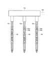
図1に示す三次元積層装置1は、基台部100に三次元形状物を製造する装置である。基台部100は、三次元形状物が形成される土台となる部材であり、三次元積層装置1で所定の位置に搬送され、表面に三次元形成物が形成される。本実施形態の基台部100は、板状の部材である。なお、基台部100は、これに限定されない。基台部100は、三次元形状物の土台となる部材を用いてもよいし、三次元形状物を付加する部材を用いてもよい。所定の位置に三次元形成物が形成されることで、部品、製品となる部材を基台部100として用いてもよい。 A three-
三次元積層装置1は、三次元積層室2と、予備室3と、積層ヘッド収納室4と、機械加工部収納室5と、ベッド10と、テーブル部11と、積層ヘッド12と、機械加工部13と、制御装置20と、を加熱ヘッド31と、機械加工部計測部32と、工具交換部33と、ノズル交換部34と、粉末導入部35と、空気排出部37と、ガス導入部38と、粉末回収部39と、温度検出部120と、質量検出部130と、を有する。 The three-
三次元積層室2は、接続された配管等の設計された連通部分以外が外部から密封されている筐体(チャンバー)である。なお、設計された連通部分は、密閉状態と開放状態を切り換えるバルブ等が設けられており、必要に応じて、三次元積層室2を密閉状態とすることができる。三次元積層室2は、ベッド10と、テーブル部11と、積層ヘッド12と、機械加工部13の一部と、加熱ヘッド31の一部と、機械加工部計測部32と、工具交換部33と、ノズル交換部34とが内部に配置されている。 The three-dimensional stacking
予備室3は、三次元積層室2に隣接して設けられている。予備室3は、接続された配管等の設計された連通部分以外が外部から密封されている。予備室3は、外部と三次元積層室2とを接続する減圧室となっている。予備室3内には、基台移動部36が設けられている。ここで、予備室3は、三次元積層室2の接続部に例えば気密性を有する扉6が設けられている。また、予備室3は、気密性を有する扉7により外部と接続されている。また、予備室3には、予備室3から空気を排出する空気排出部25が設けられている。予備室3は、扉7を開くことで、外部から必要な部材を内部に搬入することができる。また、予備室3は、扉6を開くことで、三次元積層室2との間で部材の搬入、搬出を行うことができる。 The
積層ヘッド収納室4は、三次元積層室2のZ軸方向上側の面に設けられている。積層ヘッド収納室4は、Z軸スライド部4aで三次元積層室2に対してZ軸方向(矢印102)に移動可能な状態で支持されている。積層ヘッド収納室4は、Z軸方向下側の面がベローズ18により三次元積層室2と繋がっている。ベローズ18は、積層ヘッド収納室4のZ軸方向下側の面と三次元積層室2とを繋げ、積層ヘッド収納室4のZ軸方向下側の面を三次元積層室2の一部とする。また、三次元積層室2は、ベローズ18で囲われた領域に開口が形成されている。積層ヘッド収納室4のZ軸方向下側の面とベローズ18とで囲まれた空間は、三次元積層室2と繋がり、三次元積層室2とともに密閉されている。積層ヘッド収納室4は、積層ヘッド12と、形状計測部30と、加熱ヘッド31と、を支持している。また、積層ヘッド収納室4は、積層ヘッド12のノズル23を含む一部と、加熱ヘッド31の先端部24を含む一部がZ軸方向下側の面から三次元積層室2に向けて突出している。 The stacking
積層ヘッド収納室4は、Z軸スライド部4aでZ軸方向に移動することで、保持している積層ヘッド12と、形状計測部30と、加熱ヘッド31をZ軸方向に移動させる。また、積層ヘッド収納室4は、ベローズ18を介して三次元積層室2と接続していることで、ベローズ18がZ軸方向の移動に合わせて変形し、三次元積層室2と積層ヘッド収納室4との間の密閉状態を維持できる。 The stacked
機械加工部収納室5は、三次元積層室2のZ軸方向上側の面に設けられている。また、機械加工部収納室5は、積層ヘッド収納室4に隣接して配置されている。機械加工部収納室5は、Z軸スライド部5aで三次元積層室2に対してZ軸方向(矢印104の方向)に移動可能な状態で支持されている。機械加工部収納室5は、Z軸方向下側の面がベローズ19により三次元積層室2と繋がっている。ベローズ19は、機械加工部収納室5のZ軸方向下側の面と三次元積層室2とを繋げ、機械加工部収納室5のZ軸方向下側の面を三次元積層室2の一部とする。また、三次元積層室2は、ベローズ19で囲われた領域に開口が形成されている。機械加工部収納室5のZ軸方向下側の面とベローズ19とで囲まれた空間は、三次元積層室2と繋がり、三次元積層室2とともに密閉されている。機械加工部収納室5は、機械加工部13を支持している。また、機械加工部収納室5は、機械加工部13の工具22を含む一部がZ軸方向下側の面から三次元積層室2に向けて突出している。 The machined
機械加工部収納室5は、Z軸スライド部5aでZ軸方向に移動することで、保持している機械加工部13をZ軸方向に移動させる。また、機械加工部収納室5は、ベローズ19を介して三次元積層室2と接続していることで、ベローズ19がZ軸方向の移動に合わせて変形し、三次元積層室2と機械加工部収納室5との間の密閉状態を維持できる。 The machining
ベッド10は、三次元積層室2内のZ軸方向の底部に設けられている。ベッド10は、テーブル部11を支持している。ベッド10は、各種配線や配管や駆動機構が配置されている。 The
テーブル部11は、ベッド10の上面に配置され、基台部100を支持する。テーブル部11は、Y軸スライド部15と、X軸スライド部16と、回転テーブル部17と、を有する。テーブル部11は、基台部100を取り付けて基台部100をベッド10上で移動させる。 The table unit 11 is disposed on the upper surface of the
Y軸スライド部15は、ベッド10に対してX軸スライド部16をY軸方向(矢印106の方向)に沿って移動させる。X軸スライド部16は、Y軸スライド部15の稼働部となる部材に固定されており、Y軸スライド部15に対して回転テーブル部17をX軸方向(矢印108の方向)に沿って移動させる。回転テーブル部17は、X軸スライド部16の稼働部となる部材に固定されており、基台部100を支持している。回転テーブル部17は、例えば傾斜円テーブルであり、固定台17aと、回転テーブル17bと、傾斜テーブル17cと、回転テーブル17dと、を有する。固定台17aは、X軸スライド部16の稼働部となる部材に固定されている。回転テーブル17bは、固定台17aに支持されており、Z軸方向と平行な回転軸110を回転軸として回転する。傾斜テーブル17cは、回転テーブル17bに支持されており、回転テーブル17bの支持されている面に直交する回転軸112を軸として回動される。回転テーブル17dは、傾斜テーブル17cに支持されており、傾斜テーブル17cの支持されている面に直交する回転軸114を軸として回転される。傾斜テーブル17dは、基台部100を固定している。このように、回転テーブル部17は、回転軸110、112、114を軸として各部を回転させることで、基台部100を直交する3軸周りに回転させることができる。テーブル部11は、回転テーブル部17に固定されている基台部100を、Y軸スライド部15及びX軸スライド部16により、Y軸方向及びX軸方向に移動させる。また、テーブル部11は、回転テーブル部17により回転軸110、112、114を軸として各部を回転させることで、基台部100を直交する3軸周りに回転させる。テーブル部11は、さらにZ軸方向に沿って基台部100を移動させてもよい。 The Y-
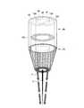
積層ヘッド12は、基台部100に向けて粉末材料を噴射し、さらに噴射した粉末材料にレーザ光を照射することにより粉末を溶融させて、溶融した粉末を基台部100上で固化させて成形層を形成する。積層ヘッド12に導入される粉末は、三次元形状物の原料となる材料の粉末である。本実施形態において、粉末は、例えば鉄、銅、アルミニウム又はチタン等の金属材料などを用いることができる。なお、粉末としては、セラミック等金属材料以外の材料を用いてもよい。積層ヘッド12は、ベッド10のZ軸方向の上側の面に対面する位置に設けられており、テーブル部11と対面している。積層ヘッド12は、Z軸方向の下部にノズル23が設置されている。積層ヘッド12は、本体46にノズル23が装着されている。 The laminating
まず、図2を用いてノズル23について説明する。図2は、積層ヘッド12のノズル23の一例を示す断面図である。図2に示すように、ノズル23は、外管41と、外管41の内部に挿入された内管42とを有する二重管である。外管41は、管状の部材であり、先端(Z軸方向下側)に向かって径が小さくなっている。内管42は、外管41の内部に挿入されている。内管42も、管状の部材であり、先端(Z軸方向下側)に向かって径が小さくなる形状である。ノズル23は、外管41の内周と内管42の外周との間が粉末材料(粉末)Pの通過する粉末流路43となる。内管42の内周面側がレーザ光Lの通過するレーザ経路44となる。ここで、ノズル23が装着されている本体46は、ノズル23と同様に二重管であり、粉末流路43とレーザ経路44も同様に形成されている。積層ヘッド12は、レーザ経路44の周囲を囲うように粉末流路43が配置されている。本実施形態では、粉末流路43が粉末を噴射する粉末噴射部となる。積層ヘッド12は、粉末導入部35から導入された粉末材料Pが粉末流路43を流れ、外管41と内管42との間の端部の開口であるノズル噴射口部45から噴射される。 First, the
また、積層ヘッド12は、光源47と光ファイバ48と集光部49とを有する。光源47は、レーザ光Lを出力する。光ファイバ48は、光源47から出力されたレーザ光Lをレーザ経路44に案内する。集光部49は、レーザ経路44に配置され、光ファイバ48から出力されたレーザ光Lの光路に配置されている。集光部49は、光ファイバ48から出力されたレーザ光Lを集光する。集光部49で集光されたレーザ光Lは、内管42の端部から出力される。 The
三次元積層装置1は、焦点位置調整部140を有する。焦点位置調整部140は、集光部49をレーザ光Lの進行方向に沿って移動させる。焦点位置調整部140は、集光部49の位置をレーザ光Lの進行方向に沿って移動させることで、レーザ光Lの焦点位置を調整することができる。なお、焦点位置調整部140としては、集光部49の焦点距離を調整する機構を用いることもできる。また、三次元積層装置1は、Z軸スライド部4aも焦点位置調整部の1つとなる。Z軸スライド部4aは、レーザ光Lの焦点位置P1と粉末材料が噴射される位置(例えば噴射される粉末材料の焦点位置P2)とが一体で移動し、焦点位置調整部140は、粉末材料が噴射される位置P2に対してもレーザ光Lの焦点位置P1を移動させることができる。三次元積層装置1は、調整する対象に応じて制御する対象を切り換えることができる。 The three-
積層ヘッド12は、粉末流路43から粉末Pを噴射し、レーザ経路44からレーザ光Lを出力する。積層ヘッド12から噴射された粉末Pは、積層ヘッド12から出力されたレーザ光Lが照射される領域に侵入し、レーザ光Lによって加熱される。レーザ光Lが照射された粉末Pは溶融した後、基台部100上に到達する。溶融した状態で基台部100上に到達した粉末Pは、冷却されて固化する。これにより、基台部100上に成形層を形成する。 The stacking
ここで、本実施形態の積層ヘッド12は、光源47から出力されたレーザ光Lを光ファイバ48で案内した光ファイバはなくてもよい。また、集光部49は、本体46に設けてもノズル23に設けても、両方に設けてもよい。本実施形態の積層ヘッド12は、効果的に加工ができるため、粉末Pを噴射する粉末流路43と、レーザ光Lを照射するレーザ経路44とを同軸に設けたがこれに限定されない。積層ヘッド12は、粉末Pを噴射する機構とレーザ光Lを照射する機構とを別体としてもよい。本実施形態の積層ヘッド12は、粉末材料にレーザ光Lを照射したが、粉末材料を溶解または焼結させることができればよく、レーザ光以外の光ビームを照射してもよい。 Here, the
次に、積層ヘッド12の粉末材料が供給される経路についてより詳細に説明する。図3は、積層ヘッドの粉末材料を供給する構造の概略構成を示す模式図である。図4は、積層ヘッドの分配部と分岐管の概略構成を示す展開図である。図5は、積層ヘッドのノズル周辺の粉末材料を供給する構造の概略構成を示す斜視図である。図6は、混合部の概略構成を示す模式図である。図7は、混合部の断面の遷移を示す説明図である。図3に示すように積層ヘッド12は、粉末導入部35から粉末供給管150を介して粉末材料が供給される。積層ヘッド12は、供給された粉末材料を粉末流路43に供給する機構として、分配部152と、複数の分岐管154と、を有する。 Next, the route through which the powder material of the
分配部(ディストリビュータ)152は、粉末供給管150から供給される粉末を均一化して分岐管154に供給する。複数の分岐管154は、分配部152と粉末流路43とを接続する管路であり、分配部152から供給された粉末を粉末流路43に供給する。本実施形態の積層ヘッド12は、図5に示すように3本の分岐管154が周方向に均等に、つまり120°間隔で配置されている。 The
分岐管154は、内部に混合部156が設けられている。混合部156は、分岐管154を流れる粉末を分岐管154内で均一化する機構であり、複数の撹拌板156aが配置されている。撹拌板156aは、分岐管154の流れ方向に沿って分岐管154の軸方向周りにねじられた構造である。また、撹拌版156aと流れ方向に隣接する撹拌版156aとは、ねじられる方向が逆となる。これにより、混合部154を通過する流体の流れは、岐管154の軸方向の位置に応じて変化する流れとなる。これにより撹拌が促進される。なお、本実施形態では、分岐管154を3本としたが、本数は特に限定されない。分岐管154は、周方向に均等に、つまり一定角度間隔で配置されていることが好ましい。 The
また、積層ヘッド12は、粉末流路43に整流装置158が設置されている。整流装置158は、3本の分岐管154から供給された粉末材料を含む流れを整流する。これにより、積層ヘッド12は、粉末流路43から噴射する粉末材料の流れを整った流れとすることができ、目的の位置により高い精度で供給することができる。 Further, the laminating
機械加工部13は、例えば成形層等を機械加工する。図1に示すように、機械加工部13は、ベッド10のZ軸方向の上側の面に対面する位置に設けられており、テーブル部11と対面している。機械加工部13は、Z軸方向の下部に工具22が装着されている。なお、機械加工部13は、ベッド10よりもZ軸方向上側で、テーブル部11による基台部100の移動可能範囲に設けられていればよく、配置位置は本実施形態の位置に限られない。 The
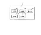
図6は、制御装置20の構成を示す模式図である。制御装置20は、三次元積層装置1の各部と電気的に接続されており、三次元積層装置1の各部の動作を制御する。制御装置20は、三次元積層室2や予備室3の外部に設置されている。制御装置20は、図6に示すように、入力部51と、制御部52と、記憶部53と、出力部54と、通信部55と、を有する。入力部51と、制御部52と、記憶部53と、出力部54と、通信部55と、の各部は電気的に接続されている。 FIG. 6 is a schematic diagram illustrating the configuration of the
入力部51は、例えば操作パネルである。作業者は、入力部51に情報や指令等を入力する。制御部52は、例えばCPU(Central Processing Unit)及びメモリである。制御部52は、三次元積層装置1の各部に、三次元積層装置1の各部の動作を制御する指令を出力する。また、制御部52には、三次元積層装置1の各部からの情報等が入力される。記憶部53は、例えばRAM(Random Access Memory)又はROM(Read Only Memory)等の記憶装置である。記憶部53には、制御部52で実行されることで各部の動作を制御する三次元積層装置1の運転プログラムや、三次元積層装置1の情報、又は三次元形状物の設計情報等が記憶される。出力部54は、例えばディスプレイである。出力部54は、例えば三次元積層装置1の各部からの情報等を表示する。通信部55は、例えばインターネット又はLAN(Local Area Network)等のような通信回線と通信して、通信回線との間で情報をやり取りする。なお、制御装置20は、少なくとも制御部52及び記憶部53を有していればよい。制御装置20は、制御部52及び記憶部53を有していれば、三次元積層装置1の各部に指令を出力することができる。 The
形状計測部30は、積層ヘッド収納室4に固定されている。形状計測部30は、積層ヘッド12に隣接して配置されている。形状計測部30は、基台部100上に形成された成形層の表面形状を計測する。形状計測部30は、例えば3Dスキャナや相対距離を計測する装置を用いることができる。形状計測部30は、例えば基台部100上の成形層の表面にレーザ光をスキャニング(走査)させ、その反射光から成形層の表面の位置情報(矢印160の距離)を算出することにより、成形層の表面形状を計測する。また、本実施形態において、形状計測部30は、積層ヘッド収納室4に取付けられているが、基台部100上に形成された成形層の表面形状を計測できればよく、別の位置に取り付けられてもよい。 The
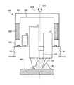
図7は、積層ヘッド収納室に設置された各部の概略構成を示す模式図である。加熱ヘッド31は、基台部100、基台部100上の成形層又は溶融した粉末P等を加熱する。加熱ヘッド31は、図1及び図7に示すように積層ヘッド12に隣接して配置されており、積層ヘッド12で加工される領域の上流側の部分(加工される前の部分)、下流側の部分(加工された後の部分)を選択的に加熱する。加熱ヘッド31は、積層ヘッド収納室4に固定されている。加熱ヘッド31は、積層ヘッド12に隣接して配置されている。加熱ヘッド31は、レーザ光162を照射し、基台部100、成形層、溶融した粉末P(溶融体A)、固化体B等を加熱する。加熱ヘッド31で成形層又は溶融した粉末Pを加熱することで、成形層又は溶融した粉末Pの温度を制御することができる。これにより、成形層又は溶融した粉末Pの急激な温度低下を抑制したり、粉末Pが溶融しやすい雰囲気(高い温度環境)を形成したりすることができる。また、加熱ヘッド31は、溶融体Aが付着する前、つまり積層ヘッド12で成形層が形成される前の成形層や基台部100を加熱することもできる。 FIG. 7 is a schematic diagram illustrating a schematic configuration of each unit installed in the stacking head storage chamber. The
図8から図10を用いて、加熱ヘッド31の一例を説明する。図8は、加熱ヘッドの概略構成を示す模式図である。図9は、加熱ヘッドの光源ユニットの概略構成を示す模式図である。図10は、加熱ヘッドの概略構成を示す斜視図である。加熱ヘッド31は、光源ユニット502と、加熱位置調整機構504と、を有する。 An example of the
光源ユニット502は、成形層や基台部100等を加熱するレーザ光162を出力する。光源ユニット502は、図9に示すように、2つの半導体レーザ540と、2つの集光部542と、光ファイバ544とを有する。2つの半導体レーザ540は、それぞれレーザ光を出力する。集光部542は、半導体レーザ540のそれぞれに対して設置されており、半導体レーザ540から出力されたレーザを集光する。光ファイバ544は、2つの集光部542のそれぞれで集光されたレーザ光が入射される。光ファイバ544は、入射されたレーザ光を加熱位置調整機構504に向けて出力する。 The
光源ユニット502は、2つの半導体レーザ540から入射された光を集光部542で集光して、1つの光ファイバ544に入射させる。これにより、光源ユニット502からは、2つの半導体レーザ540から出力されたレーザ光が合波(合流)したレーザ光162が出力される。なお、本実施形態では、2つの半導体レーザ540のレーザ光をまとめたが、半導体レーザの数は、2つに限定されず、1つでも3つ以上でもよい。光源ユニット502は、半導体レーザの数を増やすことで、レーザ光162の出力を大きくすることができる。 The
加熱位置調整機構504は、ミラー512と、ガルバノミラー514と、を有する。加熱位置調整機構504は、光源ユニット502から出力されたレーザ光162をミラー512で反射させた後、ガルバノミラー514に反射させることで向きを変えて、基台部100の領域532に照射させる。ガルバノミラー514は、ミラー520と、回転軸521を軸としてミラー520を回動させて、ミラー520の向きを変える角度位置調整機構522と、を有する。ガルバノミラー514は、回転軸521周りにミラー520を回転させることで、図10に示すように、ミラー520の向きによって、基台部100の表面においてレーザ光162が照射される位置を移動させることができる。本実施形態では、領域532の範囲でレーザ光162の照射位置を移動させることができる。加熱位置調整機構504は、ガルバノミラー514でミラー520を所定の速度パターンで回動させることで、レーザ光を走査させることができる。加熱位置調整機構504は、基台部100または成形層と加熱ヘッド31の相対移動方向である矢印528の方向に直交する方向にレーザ光を走査させる。これにより、領域532は、矢印528に直交する方向が長手方向となる。なお、加熱位置調整機構504でレーザ光を移動させる方向は、これに限定されず、必要に応じて、任意の方向にすればよい。加熱位置調整機構504は、例えば可動式ミラー514の回転軸521の向きを調整することで、レーザ光が移動可能な向きを調整することができる。 The heating
加熱ヘッド31は、光源ユニット502から出力されたレーザ光162を加熱位置調整機構504で移動させることで領域532にある基台部100または成形層を加熱する。加熱ヘッド31は、レーザ光の照射位置が移動できることで加熱を行う基台部100の位置を高い精度で調整することができ、高い精度で加熱を行うことが可能となる。 The
加熱ヘッド31は、レーザ光源として、半導体レーザ540を用いることで、波長の短いレーザ光を出力することができ、基台部100、成形層等に対するエネルギー吸収率を高くすることができる。これにより、効率よく加熱を行うことができる。また効率よく加熱できることで、発振器を小さくすることができ、光源ユニット502を小さくすることができる。また、上記実施形態では、装置が小型化できるため、光源ユニット502を加熱ヘッド31の筐体の内部に配置したが、筐体の外に配置してもよい。 The
ここで、加熱ヘッドの光源ユニットは、レーザ光源として、基板面に垂直方向にビームを出力する垂直共振器型面発光レーザ(VCSEL、Vertical Cavity Surface Emitting Laser)を用いることが好ましい。 Here, the light source unit of the heating head preferably uses a vertical cavity surface emitting laser (VCSEL) that outputs a beam in a direction perpendicular to the substrate surface as a laser light source.
図11は、加熱ヘッドの光源ユニットの他の例の概略構成を示す模式図である。光源ユニット502aは、2つの半導体レーザ540aと、合波部550と、光ファイバ544と、を有する。合波部550は、2つのコリメートレンズ551と、回折格子552と、集光部554と、を有する。2つの半導体レーザ540aは、それぞれレーザ光を出力する。半導体レーザ540aは、垂直共振器型面発光レーザである。コリメートレンズ551は、半導体レーザ540aのそれぞれに対して設置されており、半導体レーザ540aから出力されたレーザをコリメートする。回折格子552は、2つのコリメートレンズ551でコリメートされたレーザ光が入射する。回折格子552は、異なる2つの方向から入射したレーザ光の少なくとも一方を回折し、同じ方向のレーザ光とする。集光部554は、回折格子552を通過したレーザ光を集光して光ファイバ554に入射させる。光ファイバ544は、集光部554で集光されたレーザ光が入射される。光ファイバ544は、入射されたレーザ光を加熱位置調整機構504に向けて出力する。 FIG. 11 is a schematic diagram illustrating a schematic configuration of another example of the light source unit of the heating head. The
光源ユニット502aは、垂直共振器型面発光レーザを用いることで、光源ユニットをより小さくすることができる。また、上記実施形態では、レーザ光を光ファイバに入射させたが、光ファイバを用いなくてもよい。 The
また、上記実施形態の加熱ヘッドは、1軸方向に走査可能としたが、レーザ光を多軸方向に走査可能とすることが好ましい。図12は、加熱ヘッドの他の例の概略構成を示す模式図である。図12に示す加熱ヘッド31aは、光源ユニット502と、加熱位置調整機構504aと、を有する。加熱位置調整機構504aは、加熱位置調整機構504のミラー512に換えて、ガルバノミラー560を有する。 Moreover, although the heating head of the said embodiment was made to scan in a uniaxial direction, it is preferable to be able to scan a laser beam in a multiaxial direction. FIG. 12 is a schematic diagram illustrating a schematic configuration of another example of the heating head. The
加熱位置調整機構504aは、ガルバノミラー512aと、ガルバノミラー514と、を有する。加熱位置調整機構504aは、光源ユニット502から出力されたレーザ光162をガルバノミラー512aで反射させた後、ガルバノミラー514に反射させることで向きを変えて、基台部100の領域532に照射させる。ガルバノミラー512aは、ミラー560と、回転軸564を軸としてミラー560を回動させて、ミラー560の向きを変える角度位置調整機構562と、を有する。ここで、回転軸564は、回転軸521とは異なる向きの軸である。ガルバノミラー512aは、回転軸564周りにミラー562を回転させることで、図12に示すように、ミラー562の向きによって、ガルバノミラー512aに到達するレーザ光162の位置を移動させることができる。 The heating
加熱位置調整機構504aは、ガルバノミラー560のミラー562を回動させてミラー520に到達するレーザ光の位置を変化させ、さらに、ガルバノミラー514のミラー520を回動させて、基台部100に到達するレーザ光の位置を変化させることで、基台部100に到達するレーザ光の位置を二次元方向に移動させることができる。このように、加熱ヘッド31aは、レーザ光162の照射位置を基台部100の表面で二軸方向に移動させることで、二次元で照射位置を調整することができる。これにより、加熱ヘッド31aは、基台部100上で加熱を行う位置をより高い精度で調整することができ、より高い精度で加熱を行うことが可能となる。 The heating
なお、本実施形態の加熱ヘッド31aは、レーザ光を照射して対象の領域を加熱したが、これに限定されない。加熱ヘッド31aは、加熱領域を選択的に加熱することができればよく、レーザ光以外の光、例えば赤外光との光ビームを用いて加熱を行ってもよいし、電磁波等を照射して加熱を行ってもよい。 In addition, although the
温度検出部120は、加熱ヘッド31に隣接して配置されている。温度検出部120は、図7に示すように、レーザ光Lが照射される位置と、加熱ヘッド31でレーザ光162が照射され加熱される範囲を含む範囲に測定波164を出力し、温度を計測する。温度検出部120は、成形層が形成される表面の温度を計測する各種温度センサを用いることができる。 The
質量検出部130は、回転テーブル部17の回転テーブル17dに取り付けられる基台部100の質量を検出する。質量検出部130は、ロードセルを用いることができる。 The
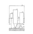
機械加工部計測部32は、機械加工部13の工具22の先端56の位置を計測する。図13は、機械加工部計測部32の一例を示す模式図である。図13に示すように、機械加工部計測部32は、光源部57と、撮像部58と、を有する。機械加工部計測部32は、光源部57と撮像部58との間に、機械加工部13の工具22の先端56を位置させる。光源部57は、例えばLEDである。撮像部58は、例えばCCD(Charge Coupled Device)カメラである。機械加工部計測部32は、光源部57と撮像部58との間に工具22の先端56を配置した状態で、光源部57から撮像部58に向けて光LIを照射し、撮像部58で画像を取得する。これにより、工具22の先端56によって、光が遮られた画像を取得することができる。機械加工部計測部32は、撮像部58で取得した画像を解析し、具体的には、光が入射した位置と光が入射していない位置の境界を検出することで、先端56の形状、位置を取得することができる。制御装置20は、取得した工具22の先端56の位置と機械加工部13の位置(機械加工部収容室5の位置)とに基づいて、機械加工部13に装着された工具22の先端の正確な位置を検出する。なお、機械加工部計測部32は、機械加工部13の先端56の位置を計測するものであれば、この構成に限られず、例えばレーザ光によって計測してもよい。 The machining
工具交換部33は、三次元積層室2の内部に配置されている。工具交換部33は、機械加工部13に装着される工具22を交換する。工具交換部33は、工具22を保持していない部分を機械加工部13と対面する位置に移動させる。その後、工具交換部33は、機械加工部13と対面する位置に工具22を把持していない部分に移動させる。その後、機械加工部13に装着されている工具22を取り外す処理を実行する。その後、機械加工部13に装着する別の工具22を把持している部分を機械加工部13に対面する位置に移動させ、機械加工部13に別の工具22を取り付ける。このように、工具交換部33は、機械加工部13の工具22を着脱することにより、機械加工部13の工具22を交換することができる。なお、工具交換部33は、機械加工部13の工具22を交換することができれば、この構成に限れられない。 The
ノズル交換部34は、三次元積層室2の内部に配置されている。ノズル交換部34は、積層ヘッド12に装着されるノズル23を交換する。ノズル交換部34は、工具交換部33と同様の構造を用いることができる。 The
粉末導入部35は、積層ヘッド12に三次元形状物の原料となる粉末材料を積層ヘッド12に導入する。図14A及び図14Bは、それぞれ粉末導入部の一例を示す模式図である。図14Aに示すように、本実施形態において、粉末Pはカートリッジ83に封入された状態で管理される。すなわち、粉末は、例えば材料の種類毎にカートリッジ83内に封入されて出荷される。カートリッジ83には材料表示部84が設けられる。材料表示部84は、例えば材料の種類などの粉末の情報を示す表示である。材料表示部84は、目視で確認できる情報に限定されず、ICチップ、二次元コード又はマーク等、読み取り器で読み取ることで情報を取得できる表示であってもよい。材料表示部84は、粉末の材料の種類を示すことができれば、これらに限られない。材料表示部84は、粉末の材料の種類以外にも、例えば粉末の粒度、重量、純度又は酸素含有量等の、三次元形状物製造の上で必要な粉末の情報を示すことができる。また、材料表示部84は、粉末が正規品であるか否かを示す情報を含んでいてもよい。 The
粉末導入部35は、粉末収納部81及び粉末識別部82を有する。粉末収納部81は、例えば箱状の部材であり、内部にカートリッジ83を収納する。粉末収納部81は、粉末を搬出するための搬送空気供給部や、粉末を積層ヘッド12に搬送する搬送経路が接続されている。粉末収納部81は、カードリッジ83が収納された場合、カードリッジ83に貯留されている粉末を積層ヘッド12に導入する。粉末識別部82は、粉末収納部81にカートリッジ83が収納されたことを検出したら、カートリッジ83の材料表示部84を読み取り、カートリッジ83に貯留されている粉末の情報を読み取る。粉末導入部35は、粉末識別部82で粉末の情報を取得することで、積層ヘッド12に既知の粉末を供給することができる。 The
ここで、粉末導入部35は、カートリッジ83内に封入された状態で管理されていない粉末を積層ヘッド12に供給するようにしてもよい。図14Bは、粉末がカートリッジに封入されない場合の粉末導入部35Aを示している。粉末導入部35Aは、粉末収納部81Aと、粉末識別部82Aと、粉末収容部81Aと粉末識別部82Aとを繋げる粉末案内管89とを有する。粉末収納部81Aは、例えば箱状の部材であり、内部に粉末Pを収納する。粉末識別部82Aは、粉末案内管89を介して供給された粉末Pを分析し、粉末Pの材料の種類、粒度、重量、純度、酸化物被膜又は酸素含有量等の、三次元形状物製造の上で必要な粉末Pの情報を計測する。粉末識別部82Aとしては、分光分析により粉末の材料を識別する分光分析装置を有し、粒度分析により粉末Pの粒度を計測する粒度分析装置、粉末の重量を計測する重量計等を用いることができる。粉末識別部82Aは、例えば計測した粉末Pの材料の種類、粒度及び重量等から、粉末の純度を計測する。また、粉末識別部82は、例えば導電率により、粉末の酸化物被膜を計測する。粉末導入部35Aも、粉末識別部82Aで粉末の情報を取得することで、積層ヘッド12に既知の粉末を供給することができる。 Here, the
基台移動部36は、予備室3に配置されている。基台移動部36は、基台部100aを予備室3内から三次元積層室2内に移動させ、三次元積層室2内の基台部100を予備室3内に移動させる。基台移動部36は、外部から予備室3内に搬入された基台部100aが取付けられる。基台移動部36は、取付けられた基台部100aを予備室3から三次元積層室2内に搬入する。より詳しくは、基台移動部36は、基台移動部36に取付けられた基台部100を、三次元積層室2内に移動させて、回転テーブル部17に取付ける。基台移動部36は、例えばロボットアームや直交軸搬送機構により、基台部100を移動させる。 The
空気排出部37は、例えば真空ポンプであり、三次元積層室2内の空気を排出する。ガス導入部38は、三次元積層室2内に所定成分のガス、例えばアルゴン、窒素等の不活性ガスを導入する。三次元積層装置1は、空気排出部37により三次元積層室2の空気を排出し、ガス導入部38により三次元積層室2にガスを導入する。これにより、三次元積層装置1は、三次元積層室2内を所望するガス雰囲気にすることができる。ここで、本実施形態において、ガス導入部38は、空気排出部37よりもZ軸方向下方に設けられる。ガス導入部38を空気排出部37よりもZ軸方向下方に設けることで、空気中の酸素等の気体よりも比重が高いアルゴンを導入するガスを用いた場合、三次元積層室2内に好適にアルゴンガスを満たすことができる。なお、導入するガスを空気よりも軽いガスとする場合、配管の配置を逆にすればよい。 The
粉末回収部39は、積層ヘッド12のノズル噴射口部45から噴射された粉末Pであって、成形層を形成しなかった粉末Pを回収する。粉末回収部39は、三次元積層室2内の空気を吸引して、空気に含まれる粉末Pを回収する。積層ヘッド12から噴射された粉末Pは、レーザ光Lにより溶融固化して、成形層を形成する。しかし、粉末Pの一部は、例えばレーザ光Lが照射されないことで、そのまま三次元積層室2内に残る場合がある。また、機械加工部13により切削されて成形層から排出された切粉が三次元積層室2に残る。粉末回収部39は、三次元積層室2に残った粉末Pや切粉を回収する。粉末回収部39は、ブラシ等機械的に粉末を回収する機構を備えていてもよい。 The
図15は、粉末回収部39の一例を示す模式図である。図15に示すように、粉末回収部39は、導入部85と、サイクロン部86と、気体排出部87と、粉末排出部88とを有する。導入部85は、例えば管状の部材であり、一方の端部が例えば三次元積層室2内に接続されている。サイクロン部86は、例えば中空の円錐台形状の部材であり、例えば鉛直方向下方に向かって径が小さくなる。導入部85の他方の端部は、サイクロン部86の外周の接線方向に沿って、サイクロン部86に接続されている。気体排出部87は、管状の部材であり、一方の端部がサイクロン部86の鉛直方向上方の端部に接続されている。粉末排出部88は、管状の部材であり、一方の端部がサイクロン部86の鉛直方向下方の端部に接続されている。 FIG. 15 is a schematic diagram illustrating an example of the
気体排出部87の他方の端部には、例えば気体を吸引するポンプが接続されている。従って、気体排出部87は、サイクロン部86から気体を吸引して、サイクロン部86を負圧にする。サイクロン部86は負圧になるため、導入部85は、三次元積層室2から気体を吸引する。導入部85は、三次元積層室2内の気体と共に、成形層を形成しなかった粉末Pを吸引する。導入部85は、サイクロン部86の外周の接線方向に沿って、サイクロン部86に接続されている。従って、導入部85に吸引された気体及び粉末Pは、サイクロン部86の内周に沿って旋回する。粉末Pは、気体よりも比重が高いため、サイクロン部86の内周の放射方向外側に遠心分離される。粉末Pは、自重により延伸方向下方の粉末排出部88に向かい、粉末排出部88から排出される。また、気体は気体排出部87により排出される。 For example, a pump for sucking gas is connected to the other end of the
粉末回収部39は、このようにして成形層を形成しなかった粉末Pを回収する。また、本実施形態における粉末回収部39は、粉末Pを比重毎に分けて回収してもよい。例えば比重が低い粉末は、自重が小さいため、粉末排出部88に向かわずに、気体排出部87に吸引される。従って、粉末回収部39は、比重毎に粉末Pを分別して回収することができる。なお、粉末回収部39は、成形層を形成しなかった粉末Pを回収することができれば、このような構成に限られない。 The
次に、三次元積層装置1による三次元形状物の製造方法について説明する。図16は、本実施形態に係る三次元積層装置1による三次元形状物の製造方法を示す模式図である。また、図16に示す製造方法は、制御装置20が各部の動作を制御することで実行することができる。本実施形態においては、台座91上に三次元形状物を製造する場合として説明する。台座91は、例えば金属製の板状部材であるが、上部に三次元形状物が製造されるものであれば、形状及び材料は任意である。台座91は、基台部100上に取付けられる。基台部100は、台座91と共に、テーブル部11の回転テーブル部17に固定される。なお、台座91を基台部100とすることもできる。 Next, the manufacturing method of the three-dimensional shape object by the three-
制御装置20は、ステップS1に示すように、テーブル部11により、基台部100上の台座91が積層ヘッド12のZ軸方向下方に配置されるように、基台部100を移動させる。 As shown in step S <b> 1, the
次に、制御装置20は、ステップS2に示すように、粉末導入部35から積層ヘッド12に粉末Pを導入し、積層ヘッド12から気体と共に粉末Pを噴射しつつ、レーザ光Lを掃射する。粉末Pは、所定の収束径をもって、基台部100上の台座91に向かって噴射される。レーザ光Lは、積層ヘッド12と台座91との間において、所定のスポット径をもって粉末Pに照射される。ここで、粉末Pの収束径のZ軸方向での位置に対するレーザ光Lのスポット径のZ軸方向での位置および粉末Pの収束径のZ軸方向での位置におけるスポット径は、例えば集光部49の位置を動かすことにより制御することができる。 Next, as shown in step S <b> 2, the
制御装置20は、積層ヘッド12によりレーザ光Lを照射しつつ粉末Pを噴射することで、ステップS3に示すように、粉末Pがレーザ光Lの照射により溶融する。溶融した粉末Pは、溶融体Aとして、基台部100上の台座91に向かってZ軸方向下方へ落下する。 The
Z軸方向下方へ落下した溶融体Aは、基台部100上の台座91の所定の位置に到達する。台座91上の溶融体Aは、台座91上の所定の位置で、例えば放冷されることにより冷却される。冷却された溶融体Aは、ステップS4に示すように、台座91上で固化体Bとして固化される。 The melt A that has dropped downward in the Z-axis direction reaches a predetermined position of the base 91 on the
制御装置20は、テーブル部11で基台部100上を所定の位置に移動させつつ、ステップS2からステップS4に示す手順で積層ヘッド12により固化体Bを基台部100上に形成する。これらの手順を繰り返すことにより、ステップS5に示すように、固化体Bは、台座91上で所定の形状を有する成形層92を形成する。 The
制御装置20は、ステップS6に示すように、台座91に形成された成形層92が機械加工部13のZ軸方向下方に配置されるように、テーブル部11により基台部100の台座91を移動させる。さらに、制御装置20は、機械加工部13により、成形層92を機械加工する。制御装置20は、機械加工部13による機械加工を実施するか否かを選択し、不要な場合は実行しなくてもよい。従って、ステップS6に示す機械加工は、制御装置20の指令によっては、実施されない場合がある。 As shown in step S <b> 6, the
次に、制御装置20は、ステップS7に示すように、テーブル部11は、制御装置20の指令により、基台部100を、例えば成形層92が積層ヘッド12のZ軸方向下方に位置するように移動させる。そして、ステップS2からステップS6に示す手順を繰り返し、成形層92の上に成形層93が順次積層され、三次元形状物が製造される。 Next, as shown in step S <b> 7, the
以上を纏めると、本実施形態に係る三次元積層装置1は、次のように三次元形状物を製造する。積層ヘッド12の粉末噴射部は、粉末Pを基台部100上の台座91に向かって噴射する。また、積層ヘッド12の内管42は、積層ヘッド12と台座91との間において、粉末Pにレーザ光Lを照射する。レーザ光Lが照射された粉末Pは、溶融され、基台部100上の台座91上で固化されて、成形層92を形成する。三次元積層装置1は、成形層92上に順次成形層93を積層し、機械加工部13により成形層92,93に適宜機械加工を加えて、三次元形状物を製造する。 In summary, the three-dimensional stacking
本実施形態において、三次元形状物は、台座91上に製造されたが、三次元形状物は、台座91上に製造されなくてもよい。三次元形状物は、例えば基台部100上に直接製造されてもよい。また、三次元積層装置1は、既存の造形物上に成形層を積層することにより、いわゆる肉盛り溶接を行ってもよい。 In the present embodiment, the three-dimensional shape object is manufactured on the
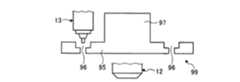
本実施形態において、機械加工部13は、例えば成形層92の表面を機械加工するが、それ以外の機械加工を行ってもよい。図17Aから図17Cは、それぞれ本実施形態に係る三次元積層装置1による三次元形状物の製造方法を示す説明図である。図17Aから図17Cは、三次元積層装置1が図17Cに示す部材99を製造する手順を示している。 In the present embodiment, the
部材99は、円板部95と、軸部97と、円錐台部98とを有する。また、部材99は、円板部95にねじ穴部96が形成されている。図17Cに示すように、円板部95は円板状の部材である。軸部97は、円板部95よりも径が小さい軸状の部材であり、円板部95の一方の面の中央部から延在する。ねじ穴部96は、円板部95の軸部97よりも外側に設けられる。円錐台部98は、軸部97の先端に設けられ、円板部95と反対方向に向かうに従って、外径が大きくなる。円錐台部98の長径は、例えば円板部95の外径と同じ大きさである。すなわち、ねじ穴部96は、円錐台部98の長径よりも内側に位置する。 The
次に、三次元積層装置1による部材99の製造手順について説明する。三次元積層装置1は、図17Aに示すように、積層ヘッド12による成形層の積層によって円板部95及び軸部97を形成する。三次元積層装置1は、円板部95及び軸部97を製造した後に、図17Bに示すように、機械加工部13によりねじ穴部96を形成する。三次元積層装置1は、ねじ穴部96を形成した後に、積層ヘッド12による成形層の積層により、軸部97上に円錐台部98を形成する。部材99は、このようにして製造される。 Next, the manufacturing procedure of the
ここで、円錐台部98の長径部分は、ねじ穴部96よりも外側に位置する。言い換えれば、ねじ穴部96は、円錐台部98により上部が覆われている。従って、例えば機械加工により部材99を製造する場合、円錐台部98の上部から円板部95に向かって、ねじ穴部96の加工工具を移動させることができない。しかし、三次元積層装置1は、円錐台部98が製造される前に、ねじ穴部96を形成する。この場合、ねじ穴部96の上部は覆われていない。従って、三次元積層装置1は、機械加工部13を、Z軸方向上部からZ軸方向に沿って移動させることにより、ねじ穴部96を加工することができる。このように、機械加工部13は、成形層の形成と機械加工とのタイミングを調整することにより、機械加工を容易にすることができる。 Here, the long diameter portion of the
次に、本実施形態に係る三次元積層装置1による三次元形状物の製造の詳細な工程について説明する。図18は、本実施形態に係る三次元積層装置1による三次元形状物の製造工程を示すフローチャートである。制御装置20は、例えば記憶部53内に記憶された三次元形状物の設計情報を読み出す。 Next, a detailed process of manufacturing a three-dimensional shape object by the three-
次に、制御装置20は、空気排出部37により三次元積層室2内の空気を排出する(ステップS11)。ここで、三次元積層室2は、扉6が閉じており、予備室3と分離されている。また、三次元積層室2は、他の外気と連通している部分も閉じられ、密封されている。制御装置20は、例えば、空気排出部37により空気を排出することで、三次元積層室2内の酸素濃度が100ppm以下、好ましくは10ppm以下とする。制御装置20は、三次元積層室2内の酸素濃度が100ppm以下とすることで、不活性状態とすることができ、10ppm以下とすることで、より確実に不活性状態とすることができる。 Next, the
次に、台座91を有する基台部100を予備室3内の基台移動部36に取付ける(ステップS12)。なお、三次元積層装置1は、ステップS12の処理を、ステップS11の処理よりも先に行ってもよい。 Next, the
制御装置20は、予備室3内の基台移動部36が取付けられたら、予備室3の扉7を閉じ、空気排出部25により、予備室3内の空気を排出する(ステップS13)。制御装置20は、空気排出部25で空気を排出することで、予備室3内の酸素濃度を低下させる。予備室3内の酸素濃度は、例えば三次元積層室2内と同じ酸素濃度になることが好ましい。 If the
制御装置20は、予備室3の空気の排出が完了したら、三次元積層室2の扉6を開き、基台移動部36により三次元積層室2内の回転テーブル部17に基台部100を取付ける(ステップS14)。基台部100は、回転テーブル部17に固定される。制御装置20は、基台部100を回転テーブル部17に取り付けたら、基台移動部36を予備室3内に戻し、扉6を閉じる。 When the discharge of the air in the
制御装置20が、基台部100を回転テーブル部17にセットしたら、ガス導入部38により三次元積層室2内にガスを導入する(ステップS15)。制御装置20は、気体導入部38により、三次元積層室2内を、導入したガス雰囲気にする。実施形態1において、気体導入部38が導入するガスは、窒素もしくはアルゴン等の不活性ガスである。気体導入部38は、三次元積層室2内の残留酸素濃度が100ppm以下となるように、不活性ガスを導入する。 If the
また、三次元積層装置1は、粉末材料の種類によっては、ステップS11、ステップS13,ステップS15を省略してもよい。例えば粉末材料の酸化によっても三次元形状物の品質等が問題にならない場合は、これらのステップを省略し、三次元積層室2及び予備室3を大気雰囲気にしてもよい。 Moreover, the three-
制御装置20は、三次元積層室2への不活性ガスの導入が完了したら、基台部100上の台座91について機械加工を行うかを判断する(ステップS16)。例えば、制御装置20は、形状計測部30に台座91の表面形状を計測させる。制御装置20は、形状計測部30の計測結果に基づき、台座91について機械加工を行うかを判断する。制御装置20は、例えば、台座91の表面粗さが所定の値より大きかった場合、台座91の機械加工を行うと判断する。ただし、制御装置20による台座91の機械加工の要否判断は、これに限られず、形状計測部30の計測結果によらなくてもよい。制御装置20は、例えば、記憶部53内に台座91の情報を記憶させておき、台座91の情報と三次元形状物の設計情報とから、台座91の加工要否を判断してもよい。また、制御装置20は、常に台座91を加工する設定としてもよい。 When the introduction of the inert gas into the three-dimensional stacking
制御装置20は、台座91の機械加工が必要であると判断した場合(ステップS16でYes)、機械加工部13により、所定の条件で台座91の機械加工を行う(ステップS17)。制御装置20は、例えば形状計測部30による台座91の形状計測結果、又は台座91の情報と三次元形状物の設計情報と等に基づき、台座91の機械加工の条件を決定する。 When the
制御装置20は、台座91の加工が必要でないと判断した場合(ステップS16でNo)、または、所定の条件で台座91の機械加工を行った場合、例えば記憶部53から読み出した三次元形状物の設計情報に基づき、成形層の形成条件を決定する(ステップS18)。成形層の形成条件とは、例えば、成形層の各層の形状、粉末Pの種類、粉末Pの噴射速度、粉末Pの噴射圧力、レーザ光Lの照射条件、粉末Pの収束径とレーザ光Lのスポット径と成形層表面の位置関係、気中で溶融した粉末Aの寸法、温度、形成中の成形層表面溶融プールBの寸法、冷却速度、又はテーブル部11による基台部100の移動速度等、成形層を形成する上で必要な条件である。 When the
制御装置20は、成形層の形成条件を決定したら、積層ヘッド12により、粉末Pを基台部100上の台座91に向かって噴射し、レーザ光Lの照射し、基台部100の加熱を開始する(ステップS19)。制御装置20は、粉末Pを噴射しつつ、レーザ光Lを照射することで、レーザ光Lにより粉末Pを溶融し、溶融した粉末Pを固化することができ、台座91上に固化体Bが形成する。また、制御装置20は、加熱ヘッド31からレーザ光Lを基台部100に照射し、基台部100の加熱を開始する。 After determining the forming conditions of the molding layer, the
制御装置20は、粉末Pを噴射しつつ、レーザ光Lを照射し、テーブル部11により基台部100を移動させることで、台座91上に成形層92を形成する(ステップS20)。制御装置20は、加熱ヘッド31で加熱を行うことで、形成された成形層92を加熱したり、固化体Bが付着する前の部分を加熱したりする。 The
制御装置20は、成形層92を形成したら、成形層92に機械加工が必要かを判断する(ステップS21)。制御装置20は、例えば形状計測部30に、成形層92の表面形状を計測させる。制御装置20は、形状計測部30の計測結果に基づき、成形層92の機械加工の要否を判断する。例えば、制御装置20は、成形層92の表面粗さが所定の値より大きかった場合、成形層92の機械加工を行うと判断する。ただし、成形層92の機械加工の要否判断の基準は、これに限られない。制御装置20は、例えば三次元形状物の設計情報と成形層の形成条件とから、成形層92の機械加工の要否を判断してもよい。例えば、制御装置20は、成形層の形成条件から算出された成形層92の表面粗さが三次元形状物の設計情報に基づく必要な表面粗さよりも大きい場合、成形層92に機械加工が必要であると判断するようにしてもよい。 After forming the
制御装置20は、成形層92の機械加工が必要ではないと判断した場合(ステップS21でNo)、ステップS24に進む。制御装置20は、成形層92の機械加工が必要である(ステップS21でYes)と判断した場合、成形層92の機械加工の加工条件を決定する(ステップS22)。例えば、制御装置20は、形状計測部30の計測結果、又は三次元形状物の設計情報と成形層の形成条件と等に基づき、加工条件を決定する。制御装置20は、成形層加工条件を決定したら、機械加工部13により、決定した加工条件に基づいて成形層92を機械加工する(ステップS23)。 When the
制御装置20は、成形層92の機械加工を行った場合、または、成形層92の機械加工が必要ではないと判断した場合、成形層92の上に更に成形層93を積層する必要があるかを判断する(ステップS24)。制御装置20は、例えば記憶部53から読み出した三次元形状物の設計情報に基づき、成形層92の上に更に成形層93を積層する必要があるかを判断する。 When the
制御装置20は、成形層93の積層が必要であると判断した場合(ステップS24でYes)、ステップS18に戻って、成形層92上に成形層93を積層する。制御装置20は、成形層93の積層が不要である(ステップS24でNo)と判断した場合、三次元形状物の製造が完了となる。 When determining that the
三次元積層装置1は、このようにして三次元形状物を製造する。本実施形態に係る三次元積層装置1は、積層ヘッド12により粉末Pを噴射して、粉末Pにレーザ光Lを照射することにより、三次元形状物を製造する。具体的には、三次元積層装置1は、対象物に向かっている粉末Pにレーザ光Lを照射し、対象物に到達する前に溶融させ、溶融体を対象物に付着させる。これにより、レーザ光Lで対象物を溶解させずに、または溶解させる量を少なくして成形層を形成することができる。これにより、製造した対象物や成形層にレーザ光が与える影響を少なくすることができ、形成されたものにさらに固化物を積層する加工を行うことができる。以上より、三次元積層装置1は、三次元形状物を高精度で製造することができる。 The three-
また、三次元積層装置1は、加熱ヘッド31を用いて、加熱位置を選択しながら、基台部または成形層を加熱することで、成形層を形成する条件をより適切に制御することができる。例えば、加熱ヘッド31を用いて、成形層のレーザ光が照射される位置を通過した領域、つまり成形層が形成された後の領域を加熱することで、成形層の減温速度を調整することができる。これにより成形層の状態をより高精度に制御することができ、成形層の強度等を調整することができる。または、加工ヘッド31は、レーザ光が照射される位置を通過する前の領域、つまり溶融体Aが付着する前の基台部または成形層を加熱することで、溶融体が付着した場合に急激に冷却されることを抑制でき、粉末をより確実に溶融体にすることができる。これにより、三次元積層装置1は、より高精度な加工が可能となり、高い精度で三次元形状物を製造することができる。 Further, the three-
さらに、三次元積層装置1は、機械加工部13により、成形層92に適宜機械加工を加えることができる。従って、三次元積層装置1は、三次元形状物を高精度で製造することができる。なお、上記実施形態では、機械加工部13を用いて、成形層や、基台部に対して機械加工を行うことで、より高い精度での加工を行うことができるが、機械加工部13を設けずに機械加工を行わなくてもよい。 Further, the three-
また、基台移動部36は、三次元積層室2の内部に基台部100を移動させる。三次元積層室2の内部は、空気が排出されている場合がある。基台移動部36は、例えば作業者が三次元積層室2の内部に入らなくても、三次元積層室2の内部に基台部100を移動させることができる。 In addition, the
ここで、三次元積層装置1は、形状計測部30を有することにより、成形層の形成条件を決定することが好ましい。図19は、本実施形態に係る三次元積層装置1による成形層の形成条件を決定する工程の一例を示すフローチャートである。図19の処理は、図18のステップS18の処理の一部として実行することができる。制御装置20は、形状計測部30により、成形層92の形状を計測する(ステップS31)。制御装置20は、積層ヘッド12に成形層92を形成させながら、形状計測部30に成形層92の形状を測定させてもよい。形状計測部30は、積層ヘッド12が固化体Bを形成しようとする箇所の形状と、その箇所に形成された固化体Bの形状との双方の形状を計測することができる。すなわち、形状計測部30は、成形層92の形成前後における表面形状を計測することができる。制御装置20は、成形層92の形状を計測したら、形状計測部30の測定結果に基づき、加熱条件を含む成形層92の形成条件を決定する(ステップS33)。 Here, it is preferable that the three-
制御装置20は、形状計測部30による成形層92の表面形状の計測結果に応じて、加熱条件を決定することで、成形層92の形状に応じて、各位置の加熱量を決定することができ、より適切に各位置を加熱することができる。これにより、各位置の温度を均一にしたり、温度変化を均一にしたりすることができ、より高精度な加工を行うことができる。 The
また、制御装置20は、形状計測部30による成形層の表面形状の計測結果に応じて、成形層の形成条件を決定し、積層ヘッド12の動作を制御する。従って、三次元積層装置1は、成形層を形成する箇所と積層ヘッド12との間の距離を一定にするなど、成形層の形成をより適切に行うことができる。さらに、三次元積層装置1は、積層ヘッド12により成形層を形成させながら、形状計測部30により成形層92の形状を計測することができる。従って、三次元積層装置1は、成形層の形成条件をより適切なものにすることができ、三次元形状物をより高精度で製造することができる。ここで、上記実施形態では、積層ヘッド12により加工について説明したが、機械加工部13による加工も同様に行うことができる。また、上記実施形態で決定する成形層の形成条件は、位置に応じ変動する条件としてもよいし、一定の条件としてもよい。 In addition, the
三次元積層装置1は、検出結果に基づいて、成形層の形成条件として、積層ヘッド12の移動経路、つまり、積層ヘッド12のZ軸方向の位置とテーブル部11による移動の相対関係を決定することが好ましい。これにより、積層される成形層の厚みや凝固部温度、積層速度を均一化することができる。 Based on the detection result, the three-
三次元積層装置1は、温度検出部120で検出した温度分布に基づいて処理動作を決定してもよい。図20は、成形層の形成条件を決定する工程の一例を示すフローチャートである。制御装置20は、温度検出部120で成形層の表面の温度分布を検出する(ステップS42)。制御装置20は、テーブル部11で基台部100を移動させつつ、温度検出部120で計測を行うことで、成形層の表面の全域の温度分布を検出することができる。制御装置20は、積層ヘッド12での加工を行う前に計測を行ってもよいし、積層ヘッド12での加工を行っている間に計測を行ってもよい。 The three-
制御装置20は、温度分布を検出したら、形状計測部30で成形層の形状(表面形状)を検出する(ステップS44)。成形層の表面形状の検出と温度分布の検出は同時に行ってもよい。 When detecting the temperature distribution, the
制御装置20は、成形層の形状を検出したら、成形層の形状と温度分布とに基づいて、温度検出部で温度を検出する検出位置を特定し(ステップS46)、特定した位置の温度を検出する(ステップS48)。制御装置20は、検出した温度に基づいて加熱条件を含む成形層の形成条件を決定し(ステップS49)、本工程を終了する。 When detecting the shape of the molding layer, the
三次元積層装置1は、特定の位置、例えば冷えにくいところや温まりやすいところについて温度を計測して加熱条件を決定することで、各位置の温度や温度変化を高い精度で制御することができ、より適切な加工を行うことができる。 The three-
さらに、三次元積層装置1は、温度分布と形状に基づいて加工条件として積層ヘッド12の移動経路を決定することで、つまり温度分布も加味して加工条件を決定することで、積層される成形層の厚みや凝固部温度、積層速度を均一化することができる。つまり冷えにくいところや温まりやすいところを把握して、加工条件を決定的、より均一な加工を行うことが可能となる。 Further, the three-
また、図20に示す例では、温度を再度検出したが、ステップS46とステップS48の処理は、行わずに加熱条件を含む成形層の形成条件を決定してもよい。三次元積層装置1は、温度分布と形状に基づいて加熱条件を決定することで、各位置の温度や温度変化を高い精度で制御することができる。 In the example shown in FIG. 20, the temperature is detected again. However, the forming layer forming conditions including the heating conditions may be determined without performing the processes in steps S46 and S48. The three-
また、三次元積層装置1は、質量検出部130の検出結果を用いて、処理動作を決定してもよい。例えば、形成した成形物によって生じる質量の変化を検出し、製造している三次元積層物を評価するようにしてもよい。具体的には、形成した大きさと質量の変化を検出することで、三次元積層物の密度を算出することができ、三次元積層物に空隙が形成されていないかを判定することができる。また、三次元積層装置1は、質量検出部130の重量に基づいて、基台部100に異物、具体的には、溶融しなかった粉末材料や機械加工部13による加工で生成された切粉が付着していないかを検出することもできる。これにより、粉末回収部39の動作の制御に用いることができる。 Further, the three-
三次元積層装置は、形成条件を制御するためのパラメータを検出する装置として、さらに他の検出部を備えていてもよい。図21は、三次元積層装置の積層ヘッドの周辺部の他の例を示す模式図である。図21に示す三次元積層装置は、積層ヘッドのレーザ光の経路の周辺に、温度検出部120aと、ハーフミラー182と、プラズマ発光検出部190と、反射光検出部192と、を有する。ハーフミラー182は、光源47と、集光部49との間に配置され、光源47から集光部49に向かうレーザ光を透過させ、集光部49から光源47に向かうレーザ光を反射する。つまりハーフミラー182は、基台部100や成形層で反射したレーザ光を所定の方向に反射する。 The three-dimensional laminating apparatus may further include another detection unit as an apparatus for detecting a parameter for controlling the formation conditions. FIG. 21 is a schematic diagram illustrating another example of the peripheral portion of the stacking head of the three-dimensional stacking apparatus. The three-dimensional laminating apparatus shown in FIG. 21 includes a
プラズマ発光検出部190は、基台部100や成形層、供給される粉末にレーザ光Lが照射されることで発生するプラズマを検出する。反射光検出部192は、ハーフミラー182で反射されたレーザ光Lを検出する。また、温度検出部120aは、ミラー182で反射されて映るレーザ光の照射位置の状態に基づいて温度を検出する。 The plasma light
次に、図22から図24を用いて、各部を用いて実行する制御の一例を説明する。図22は、成形層の形成条件、具体的には加熱ヘッドによる加熱条件を決定する工程の一例を示すフローチャートである。図22から図24の処理は、積層ヘッドによる加工時に並行して行うことが好ましいが、形成条件を決める際に実行してもよい。制御装置20は、温度検出部120aで温度を検出し(ステップS102)、検出した結果に基づいて、加熱条件を決定し(ステップS104)、本処理を終了する。制御装置20は、温度検出部120aで検出した結果に基づいて加熱ヘッド31による加熱の条件を決定することで、成形層の温度をより均一にすることができより高精度な加工を行うことができる。なお、温度検出部120の場合も同様の制御を行うことができる。 Next, an example of control executed using each unit will be described with reference to FIGS. FIG. 22 is a flowchart illustrating an example of a process for determining a forming layer formation condition, specifically, a heating condition by a heating head. The processing of FIGS. 22 to 24 is preferably performed in parallel with the processing by the stacking head, but may be executed when determining the formation conditions. The
図23は、成形層の形成条件を決定する工程の一例を示すフローチャートである。制御装置20は、プラズマ発光検出部190でプラズマ発光を検出し(ステップS112)、検出したプラズマ発光に基づいて、加熱条件を決定し(ステップS114)、本処理を終了する。制御装置20は、プラズマ発光検出部190で検出した結果に基づいて加熱ヘッド31による加熱の条件を決定することでも、成形層の温度をより均一にすることができより高精度な加工を行うことができる。ここで、制御装置20は、プラズマ発光検出部190でプラズマ発光を検出することで、レーザの焦点位置の温度を監視することができる。また噴射された粉末がレーザ光に入り溶融する場合に発光するプラズマを検出することで気中の粉末溶融状態を監視することができる。 FIG. 23 is a flowchart illustrating an example of a process for determining the forming condition of the molding layer. The
図24は、成形層の形成条件を決定する工程の一例を示すフローチャートである。制御装置20は、反射光検出部192で反射光を検出し(ステップS122)、検出した反射光に基づいて、加熱条件を決定し(ステップS124)、本処理を終了する。制御装置20は、反射光検出部192で検出した結果に基づいて加熱ヘッド31による加熱の条件を決定することでも、成形層の温度をより均一にすることができより高精度な加工を行うことができる。ここで、制御装置20は、反射光検出部192で反射光を検出することで、溶融体Aが付着する位置の温度を監視することができる。 FIG. 24 is a flowchart illustrating an example of a process for determining the forming condition of the molding layer. The
ここで、三次元積装置1は、温度検出部120及び加熱ヘッド31を積層ヘッド12に対して、Z軸周りに回転できるようにすることが好ましい。これにより、テーブル部11の移動方向に応じて、積層ヘッド12と温度検出部120及び加熱ヘッド31との相対位置を一定としたり、切り換えたりすることができる。また、三次元積装置1は、温度検出部120及び加熱ヘッド31を積層ヘッド12に対して2つ設け、積層ヘッド12を挟み込むように配置してもよい。 Here, it is preferable that the three-
図25は、積層ヘッド収納室の他の例を示す模式図である。図25に示す積層ヘッド収納室504は、積層ヘッド12と、形状計測部30と、加熱ヘッド31とを支持している。積層ヘッド収納室504は、積層ヘッド12と、形状計測部30と、加熱ヘッド31とを支持している部分が切換機構580となる。切換機構580は、固定部581と、可動部582と、回転機構584と、シール部586とを有する。固定部581は、Z軸スライド部4aに支持され、底面がベローズ18と繋がっている。可動部582は、固定部581に内蔵され、積層ヘッド12と、形状計測部30と、加熱ヘッド31とを固定している。回転機構584は、固定部581に対して可動部582を軸590周りに回転させる。シール586は、鉛直方向下側の面、つまり、三次元積層室2に露出している面の固定部581と可動部582との間を回転自在の状態で密閉している。 FIG. 25 is a schematic diagram illustrating another example of the stacked head storage chamber. A laminated
切換機構580は、固定部581に対して可動部582を回転させることで、可動部582が支持している積層ヘッド12と加熱ヘッド31との相対位置を切り換えることができる。これにより、切換機構580は、積層ヘッド12と基台部100との相対移動方向、つまりテーブル部11が基台部100を移動させる方向に対して、積層ヘッド12が加熱ヘッド31よりも上流側にある状態と、積層ヘッド12が加熱ヘッド31よりも下流側にある状態と、を切り換えることができる。つまり、同じ方向に基台部100が移動している場合は、可動部582を180度回転させることで積層ヘッド12と加熱ヘッド31との加工位置に対する前後関係を入れ替えることができる。これにより、加熱ヘッド31が、積層ヘッド12を通過する前(成形層の形成を行う前)の基台部100または成形層を加熱するか、積層ヘッド12を通過した後(成形層の形成を行った後)の基台部100または成形層を加熱するかを切り換えることができる。 The
図26は、三次元積層装置による処理動作の一例を示すフローチャートである。制御装置20は、積層ヘッド12と基台部100との相対移動方向を検出し(ステップS170)、加熱ヘッド31の加熱領域を特定する(ステップS172)。加熱ヘッド31の加熱領域とは、積層ヘッド12で加工される基台部に対して設定されており、積層ヘッド12を通過する前の基台部100または成形層を加熱する領域、積層ヘッド12を通過した後の基台部100または成形層を加熱する領域がある。 FIG. 26 is a flowchart illustrating an example of a processing operation performed by the three-dimensional stacking apparatus. The
制御装置20は、加熱ヘッド31が積層ヘッド12に対して適正な位置であるかを判定する(ステップS174)。つまり、積層ヘッド12と基台部100との相対移動方向と加熱領域と現状の積層ヘッド12と加熱ヘッド31との相対位置に基づいて、加熱ヘッドが加熱領域を加熱できる位置であるかを判定する。 The
制御装置20は、加熱ヘッド31が積層ヘッド12に対して適正な位置である(ステップS174でYes)と判定した場合、ステップS178に進む。制御装置20は、加熱ヘッド31が積層ヘッド12に対して適正な位置ではない(ステップS174でNo)と判定した場合、切換機構580で、加熱ヘッド31と積層ヘッドとの相対位置を切り換え(ステップS176)、ステップS178に進む。 When the
制御装置20は、ステップS174でYesまたはステップS176の処理を行った場合、積層ヘッド12と基台部100との相対移動方向が変更されたかを判定する(ステップS178)。制御装置20は、移動方向が変更した(ステップS178でYes)と判定した場合、ステップS170に戻る。制御装置20は、移動方向が変更していない(ステップS178でNo)と判定した場合、製造終了かを判定する(ステップS179)。制御装置20は、製造終了ではない(ステップS179でNo)と判定した場合、ステップS178に戻り、製造終了である(ステップS179でYes)と判定した場合、本処理を終了する。 When the
三次元積層装置1は、図26に示す処理を行い、積層ヘッドと基台部との相対移動方向に応じて、積層ヘッドと加熱ヘッドとの相対位置を切り換えることで、加工位置に対する積層ヘッドと加熱ヘッドとの関係を設定に応じた位置にすることができる。これにより、積層ヘッドと基台部との相対移動によって、積層ヘッドが加工する位置に対して加熱ヘッドで加熱する位置が変化することを抑制できる。これにより、より高精度な加工を行うことができる。 The three-
以上、本発明の実施形態を説明したが、これらの実施形態の内容によりこれらの実施形態が限定されるものではない。また、前述した構成要素には、当業者が容易に想定できるもの、実質的に同一のもの、いわゆる均等の範囲のものが含まれる。さらに、前述した構成要素は適宜組み合わせることが可能である。さらに、前述した実施形態等の要旨を逸脱しない範囲で構成要素の種々の省略、置換又は変更を行うことができる。例えば、三次元積層装置1は、積層ヘッド12により粉末Pを噴射して、粉末Pにレーザ光Lを照射する構成に限られない。三次元積層装置1は、粉末Pを供給して粉末Pにレーザ光Lを照射することにより成形層を形成し、成形層に適宜機械加工を加えることができればよい。例えば、三次元積層装置1は、粉末供給部により粉末層を形成し、粉末層の一部にレーザ光Lを照射して粉末を焼結させることにより、成形層を形成するものであってもよい。 As mentioned above, although embodiment of this invention was described, these embodiment is not limited by the content of these embodiment. In addition, the above-described constituent elements include those that can be easily assumed by those skilled in the art, those that are substantially the same, and those in a so-called equivalent range. Furthermore, the above-described components can be appropriately combined. Furthermore, various omissions, substitutions, or changes of the constituent elements can be made without departing from the spirit of the above-described embodiments and the like. For example, the three-
1 三次元積層装置
2 三次元積層室
3 予備室
4 積層ヘッド収納室
4a、5a Z軸スライド部
5 機械加工部収納室
6、7 扉
10 ベッド
11 テーブル部
12 積層ヘッド
13 機械加工部
15 Y軸スライド部
16 X軸スライド部
17 回転テーブル部
18、19 ベローズ
20 制御装置
22 工具
23 ノズル
24 先端部
25 空気排出部
30 形状計測部
31、31a 加熱ヘッド
32 機械加工部計測部
33 工具交換部
34 ノズル交換部
35、35A 粉末導入部
36 基台移動部
37 空気排出部
38 ガス導入部
39 粉末回収部
41 外管
42 内管
43 粉末流路
44 レーザ経路
46 本体
47 光源
48 光ファイバ
49 集光部
51 入力部
52 制御部
53 記憶部
54 出力部
55 通信部
56 先端
57 光源部
58 撮像部
81、81A 粉末収納部
82、82A 粉末識別部
83 カートリッジ
84 材料表示部
85 導入部
86 サイクロン部
87 気体排出部
88 粉末排出部
91 台座
92、93 成形層
95 円板部
96 ねじ穴部
97 軸部
98 円錐台部
99 部材
100 基台部
102、104、106、108 矢印
110、112、114 回転軸
120、120a 温度検出部
130 質量検出部
140 焦点位置調整部
150 粉末供給管
152 分配部
154 分岐管
156 混合部
156a 撹拌板
158 整流装置
162 レーザ光
164 測定波
182 ハーフミラー
190 プラズマ発光検出部
192 反射光検出部
502、502a 光源ユニット
504、504a 加熱位置調整機構
512、520、560 ミラー
514、514a ガルバノミラー
522、562 角度位置調整機構
532 領域
540、540a 半導体レーザ
542 集光部
544 光ファイバ
550 合波部
551 コリメートレンズ
552 回折格子
554 集光部
A 溶融体
B 固化体
L レーザ光
P 粉末
P1、P2 位置DESCRIPTION OF
47
Claims (22)
Translated fromJapanese前記基台部に向かって粉末材料を噴射する粉末供給部と、
前記粉末材料に光ビームを照射し、前記光ビームが照射された前記粉末材料の少なくとも一部を溶融固化させて前記成形層を形成する光照射部と、
前記基台部または成形層の前記光ビームが照射される位置を通過した下流側領域または前記光ビームが照射される位置を通過する前の上流側領域を選択的に加熱する加熱部と、
前記粉末供給部、前記光照射部及び前記加熱部の動作を制御する制御装置と、を有し、
前記加熱部は、前記光照射部の側方に回転可能に支持され、
前記光照射部の光源と前記加熱部の光源とは、互いに異なる、
三次元積層装置。A three-dimensional laminating apparatus that forms a three-dimensional shape by laminating a molding layer on a base part,
A powder supply part forinjecting a powder materialtoward the base part ;
A light irradiation unit which irradiates a light beam to form the molded layer at least a portion of the powder material the light beam is irradiated bymelting solidifiedbefore Symbol powder material,
A heating unit that selectively heats thedownstream region of the base part or the molding layer that has passed the position irradiated with the light beam or theupstream region before passing the position irradiated with the light beam;
The powder feeder,have a, and a control unit for controlling the operation of the light irradiation unit and the heatingunit,
The heating unit is rotatably supported to the side of the light irradiation unit,
The light source of the light irradiation unit and the light source of the heating unit are different from each other.
Three-dimensional laminating device.
前記光照射部は、前記粉末供給部から前記基台部に向けて移動する前記粉末材料に光ビームを照射し、前記粉末材料を溶融させて、溶融した前記粉末材料を前記基台部上で固化させて前記成形層を形成する請求項1に記載の三次元積層装置。The powder supply unit injects the powder material toward the base unit,
The light irradiation unit irradiates the powder material moving from the powder supply unit toward the base unit with a light beam, melts the powder material, and causes the powder material to melt on the base unit. The three-dimensional laminating apparatus according to claim 1, wherein the molding layer is formed by solidification.
前記制御装置は、前記移動機構によって前記基台部に対して前記光照射部及び前記粉末供給部が通過する経路を決定する請求項2または3に記載の三次元積層装置。A moving mechanism for relatively moving the light irradiation unit, the powder supply unit, and the base unit;
The said control apparatus is a three-dimensional laminating apparatus of Claim 2 or 3 which determines the path | route through which the said light irradiation part and the said powder supply part pass with respect to the said base part by the said moving mechanism.
前記光源ユニットから出力する光ビームを照射して加熱を行う請求項1から4のいずれか一項に記載の三次元積層装置。The heating unit includes a light source unit that outputs a light beam,
The three-dimensional laminating apparatus according to any one of claims 1 to 4, wherein heating is performed by irradiating a light beam output from the light source unit.
複数の前記半導体レーザで出力され、それぞれの前記集光部で集光されたレーザ光が1つの光ファイバに入射される請求項9に記載の三次元積層装置。The light source unit includes a plurality of the semiconductor lasers and the condensing unit,
The three-dimensional laminating apparatus according to claim9 , wherein laser light output from a plurality of the semiconductor lasers and condensed by each of the condensing units is incident on one optical fiber.
前記集光部は、複数の前記半導体レーザのそれぞれに配置されたコリメートレンズと、
複数の前記コリメートレンズでコリメートされたレーザ光を合波して前記光ファイバに入射させる合波部と、を有する請求項11に記載の三次元積層装置。A plurality of the semiconductor lasers;
The condensing unit includes a collimating lens disposed in each of the plurality of semiconductor lasers,
The three-dimensional laminating apparatus according to claim11 , further comprising: a multiplexing unit configured to multiplex laser beams collimated by the plurality of collimating lenses and to enter the optical fiber.
前記制御装置は、前記温度検出部による前記成形層の表面温度の計測結果に応じて、前記加熱部による加熱を制御する請求項1から12のいずれか一項に記載の三次元積層装置。A temperature detection unit for detecting the temperature and distribution of the surface of the molding layer;
The three-dimensional laminating apparatus according to any one of claims 1 to12 , wherein the control device controls heating by the heating unit in accordance with a measurement result of a surface temperature of the molding layer by the temperature detection unit.
前記制御装置は、前記温度検出部による前記成形層の表面温度の計測結果と、前記形状計測部による前記成形層の表面形状の計測結果との両方に基づいて、前記加熱部による加熱を制御する請求項12に記載の三次元積層装置。Having a shape measuring unit for measuring the surface shape of the molding layer;
The control device controls heating by the heating unit based onboth the measurement result of the surface temperature of the molding layer by the temperature detection unit and the measurement resultof the surface shape of the molding layer by the shape measurement unit. The three-dimensional laminating apparatus according to claim 12.
前記制御装置は、前記プラズマ発光検出部による計測結果に応じて、前記加熱部による加熱を制御する請求項1から15のいずれか一項に記載の三次元積層装置。Having a plasma emission detector for detecting plasma emission on the surface of the molding layer;
The three-dimensional laminating apparatus according to any one of claims 1 to15 , wherein the control device controls heating by the heating unit in accordance with a measurement result by the plasma light emission detection unit.
前記制御装置は、前記反射光検出部による計測結果に応じて、前記加熱部による加熱を制御する請求項1から16のいずれか一項に記載の三次元積層装置。A reflected light detection unit for detecting reflected light from the surface of the molding layer;
The three-dimensional laminating apparatus according to any one of claims 1 to16 , wherein the control device controls heating by the heating unit in accordance with a measurement result by the reflected light detection unit.
前記制御装置は、前記下流側領域を加熱するか前記上流側領域を加熱するかに応じて、前記切換機構により前記光照射部と前記加熱部の相対位置を制御する請求項1に記載の三次元積層装置。A switching mechanism for switching a relative position between the light irradiation unit and the heating unit;
The tertiary according to claim1, wherein the control device controls a relative position between the light irradiation unit and the heating unit by the switching mechanism accordingto whether the downstream region is heated or the upstream region is heated. Original laminating equipment.
前記基台部に向かって粉末材料を粉末供給部から噴射し、
前記粉末材料に第1の光源を含む光照射部から光ビームを照射することにより、前記光ビームが照射された前記粉末材料の少なくとも一部を溶融固化させて前記基台部上に成形層を形成し、
前記基台部または成形層の前記光ビームが照射される位置を通過した下流側領域または前記光ビームが照射される位置を通過する前の上流側領域に、前記第1の光源とは異なる第2の光源を含む加熱部から光ビームを照射して選択的に加熱し、
前記下流側領域を加熱する場合は、前記加熱部を前記光照射部に対して回転させ第1の相対位置に配置し、前記上流側領域を加熱する場合は、前記加熱部を前記光照射部に対して回転させ前記第1の相対位置とは異なる第2の相対位置に配置する、三次元積層方法。A three-dimensional lamination method of forming a three-dimensional shape by laminating a molding layer on a base part,
Toward the base portionbyinjecting powdered material fromflour powder supplyunit,
By irradiating the light beamfrom the light irradiation unit including a first light sourcebefore Symbol powdermaterial, molded layer on the base part by at least a portion is melted and solidified in the powder material the light beam is irradiated Form the
In thedownstream region that has passed through the position where the light beam is irradiated on the base part or the molding layer, or in theupstream region that has not passed through the position where the light beam is irradiated,the first light source is different. Selectively irradiating witha light beamfrom a heating unit including two light sources ,
When heating the downstream region, the heating unit is rotated with respect to the light irradiation unit and arranged at the first relative position, and when heating the upstream region, the heating unit is moved to the light irradiation unit. The three-dimensional stacking methodis arranged so as to be rotated at a second relative position different from the first relative position .
Priority Applications (9)
| Application Number | Priority Date | Filing Date | Title |
|---|---|---|---|
| JP2014074058AJP6254036B2 (en) | 2014-03-31 | 2014-03-31 | Three-dimensional laminating apparatus and three-dimensional laminating method |
| KR1020187012290AKR20180049219A (en) | 2014-03-31 | 2015-03-20 | Three-dimensional lamination device and three-dimensional lamination method |
| CN201580017061.1ACN106163703B (en) | 2014-03-31 | 2015-03-20 | Three-dimensional laminating apparatus and three-dimensional laminating method |
| KR1020167027064AKR20160129871A (en) | 2014-03-31 | 2015-03-20 | Three-dimensional lamination device and three-dimensional lamination method |
| EP15773604.2AEP3127685B1 (en) | 2014-03-31 | 2015-03-20 | Three-dimensional deposition device and three-dimensional deposition method |
| PCT/JP2015/058496WO2015151864A1 (en) | 2014-03-31 | 2015-03-20 | Three-dimensional lamination device and three-dimensional lamination method |
| MX2016012702AMX377675B (en) | 2014-03-31 | 2015-03-20 | DEVICE FOR THREE-DIMENSIONAL DEPOSITION AND THREE-DIMENSIONAL DEPOSITION METHOD. |
| US15/129,923US10898971B2 (en) | 2014-03-31 | 2015-03-20 | Three-dimensional deposition device and three-dimensional deposition method |
| TW104110108ATWI600485B (en) | 2014-03-31 | 2015-03-27 | Three-dimensional layering device and three-dimensional layering method |
Applications Claiming Priority (1)
| Application Number | Priority Date | Filing Date | Title |
|---|---|---|---|
| JP2014074058AJP6254036B2 (en) | 2014-03-31 | 2014-03-31 | Three-dimensional laminating apparatus and three-dimensional laminating method |
Publications (3)
| Publication Number | Publication Date |
|---|---|
| JP2015196164A JP2015196164A (en) | 2015-11-09 |
| JP2015196164A5 JP2015196164A5 (en) | 2017-01-19 |
| JP6254036B2true JP6254036B2 (en) | 2017-12-27 |
Family
ID=54240194
Family Applications (1)
| Application Number | Title | Priority Date | Filing Date |
|---|---|---|---|
| JP2014074058AActiveJP6254036B2 (en) | 2014-03-31 | 2014-03-31 | Three-dimensional laminating apparatus and three-dimensional laminating method |
Country Status (8)
| Country | Link |
|---|---|
| US (1) | US10898971B2 (en) |
| EP (1) | EP3127685B1 (en) |
| JP (1) | JP6254036B2 (en) |
| KR (2) | KR20180049219A (en) |
| CN (1) | CN106163703B (en) |
| MX (1) | MX377675B (en) |
| TW (1) | TWI600485B (en) |
| WO (1) | WO2015151864A1 (en) |
Families Citing this family (420)
| Publication number | Priority date | Publication date | Assignee | Title |
|---|---|---|---|---|
| US10378106B2 (en) | 2008-11-14 | 2019-08-13 | Asm Ip Holding B.V. | Method of forming insulation film by modified PEALD |
| US9394608B2 (en) | 2009-04-06 | 2016-07-19 | Asm America, Inc. | Semiconductor processing reactor and components thereof |
| US8802201B2 (en) | 2009-08-14 | 2014-08-12 | Asm America, Inc. | Systems and methods for thin-film deposition of metal oxides using excited nitrogen-oxygen species |
| US9312155B2 (en) | 2011-06-06 | 2016-04-12 | Asm Japan K.K. | High-throughput semiconductor-processing apparatus equipped with multiple dual-chamber modules |
| US10364496B2 (en) | 2011-06-27 | 2019-07-30 | Asm Ip Holding B.V. | Dual section module having shared and unshared mass flow controllers |
| US10854498B2 (en) | 2011-07-15 | 2020-12-01 | Asm Ip Holding B.V. | Wafer-supporting device and method for producing same |
| US20130023129A1 (en) | 2011-07-20 | 2013-01-24 | Asm America, Inc. | Pressure transmitter for a semiconductor processing environment |
| US9017481B1 (en) | 2011-10-28 | 2015-04-28 | Asm America, Inc. | Process feed management for semiconductor substrate processing |
| US9659799B2 (en) | 2012-08-28 | 2017-05-23 | Asm Ip Holding B.V. | Systems and methods for dynamic semiconductor process scheduling |
| US9021985B2 (en) | 2012-09-12 | 2015-05-05 | Asm Ip Holdings B.V. | Process gas management for an inductively-coupled plasma deposition reactor |
| US10714315B2 (en) | 2012-10-12 | 2020-07-14 | Asm Ip Holdings B.V. | Semiconductor reaction chamber showerhead |
| US20160376700A1 (en) | 2013-02-01 | 2016-12-29 | Asm Ip Holding B.V. | System for treatment of deposition reactor |
| US9484191B2 (en) | 2013-03-08 | 2016-11-01 | Asm Ip Holding B.V. | Pulsed remote plasma method and system |
| US9589770B2 (en) | 2013-03-08 | 2017-03-07 | Asm Ip Holding B.V. | Method and systems for in-situ formation of intermediate reactive species |
| EP3415254A1 (en) | 2013-06-10 | 2018-12-19 | Renishaw PLC | Selective laser solidification apparatus and method |
| GB201310398D0 (en) | 2013-06-11 | 2013-07-24 | Renishaw Plc | Additive manufacturing apparatus and method |
| US9240412B2 (en) | 2013-09-27 | 2016-01-19 | Asm Ip Holding B.V. | Semiconductor structure and device and methods of forming same using selective epitaxial process |
| US10683571B2 (en) | 2014-02-25 | 2020-06-16 | Asm Ip Holding B.V. | Gas supply manifold and method of supplying gases to chamber using same |
| US10167557B2 (en) | 2014-03-18 | 2019-01-01 | Asm Ip Holding B.V. | Gas distribution system, reactor including the system, and methods of using the same |
| US11015245B2 (en) | 2014-03-19 | 2021-05-25 | Asm Ip Holding B.V. | Gas-phase reactor and system having exhaust plenum and components thereof |
| JP6359316B2 (en) | 2014-03-31 | 2018-07-18 | 三菱重工業株式会社 | Three-dimensional laminating apparatus and three-dimensional laminating method |
| US10618131B2 (en) | 2014-06-05 | 2020-04-14 | Nlight, Inc. | Laser patterning skew correction |
| US10858737B2 (en) | 2014-07-28 | 2020-12-08 | Asm Ip Holding B.V. | Showerhead assembly and components thereof |
| US9890456B2 (en) | 2014-08-21 | 2018-02-13 | Asm Ip Holding B.V. | Method and system for in situ formation of gas-phase compounds |
| US9657845B2 (en) | 2014-10-07 | 2017-05-23 | Asm Ip Holding B.V. | Variable conductance gas distribution apparatus and method |
| US10941490B2 (en) | 2014-10-07 | 2021-03-09 | Asm Ip Holding B.V. | Multiple temperature range susceptor, assembly, reactor and system including the susceptor, and methods of using the same |
| KR102263121B1 (en) | 2014-12-22 | 2021-06-09 | 에이에스엠 아이피 홀딩 비.브이. | Semiconductor device and manufacuring method thereof |
| US10529542B2 (en) | 2015-03-11 | 2020-01-07 | Asm Ip Holdings B.V. | Cross-flow reactor and method |
| US10276355B2 (en) | 2015-03-12 | 2019-04-30 | Asm Ip Holding B.V. | Multi-zone reactor, system including the reactor, and method of using the same |
| GB201505458D0 (en) | 2015-03-30 | 2015-05-13 | Renishaw Plc | Additive manufacturing apparatus and methods |
| US10458018B2 (en) | 2015-06-26 | 2019-10-29 | Asm Ip Holding B.V. | Structures including metal carbide material, devices including the structures, and methods of forming same |
| US10600673B2 (en) | 2015-07-07 | 2020-03-24 | Asm Ip Holding B.V. | Magnetic susceptor to baseplate seal |
| US10083836B2 (en) | 2015-07-24 | 2018-09-25 | Asm Ip Holding B.V. | Formation of boron-doped titanium metal films with high work function |
| US9960072B2 (en) | 2015-09-29 | 2018-05-01 | Asm Ip Holding B.V. | Variable adjustment for precise matching of multiple chamber cavity housings |
| US10211308B2 (en) | 2015-10-21 | 2019-02-19 | Asm Ip Holding B.V. | NbMC layers |
| JP2019501781A (en)* | 2015-11-06 | 2019-01-24 | アイピージー フォトニクス コーポレーション | Modular laser processing housing and system |
| US10322384B2 (en) | 2015-11-09 | 2019-06-18 | Asm Ip Holding B.V. | Counter flow mixer for process chamber |
| WO2017091505A1 (en) | 2015-11-23 | 2017-06-01 | Nlight, Inc. | Fine-scale temporal control for laser material processing |
| US11179807B2 (en) | 2015-11-23 | 2021-11-23 | Nlight, Inc. | Fine-scale temporal control for laser material processing |
| US10688596B2 (en)* | 2015-12-18 | 2020-06-23 | Illinois Tool Works Inc. | Wire manufactured by additive manufacturing methods |
| US11139308B2 (en) | 2015-12-29 | 2021-10-05 | Asm Ip Holding B.V. | Atomic layer deposition of III-V compounds to form V-NAND devices |
| FR3046367A1 (en)* | 2015-12-31 | 2017-07-07 | Nantes Ecole Centrale | DEVICE FOR ADDITIVE MANUFACTURING BY PROJECTION AND POWDER FUSION |
| DE102017102355A1 (en)* | 2016-02-09 | 2017-08-10 | Jtekt Corporation | MANUFACTURING DEVICE AND MANUFACTURED PROCESS FOR MANUFACTURING |
| US10468251B2 (en) | 2016-02-19 | 2019-11-05 | Asm Ip Holding B.V. | Method for forming spacers using silicon nitride film for spacer-defined multiple patterning |
| US10529554B2 (en) | 2016-02-19 | 2020-01-07 | Asm Ip Holding B.V. | Method for forming silicon nitride film selectively on sidewalls or flat surfaces of trenches |
| US10831180B2 (en)* | 2016-02-25 | 2020-11-10 | General Electric Company | Multivariate statistical process control of laser powder bed additive manufacturing |
| US10501866B2 (en) | 2016-03-09 | 2019-12-10 | Asm Ip Holding B.V. | Gas distribution apparatus for improved film uniformity in an epitaxial system |
| US10343920B2 (en) | 2016-03-18 | 2019-07-09 | Asm Ip Holding B.V. | Aligned carbon nanotubes |
| US9892913B2 (en) | 2016-03-24 | 2018-02-13 | Asm Ip Holding B.V. | Radial and thickness control via biased multi-port injection settings |
| US20180162053A1 (en)* | 2016-03-25 | 2018-06-14 | Technology Research Association For Future Additive Manufacturing | Three-dimensional laminating and shaping apparatus, control method of three-dimensional laminating and shaping apparatus, and control program of three-dimensional laminating and shaping apparatus |
| US10865475B2 (en) | 2016-04-21 | 2020-12-15 | Asm Ip Holding B.V. | Deposition of metal borides and silicides |
| US10190213B2 (en) | 2016-04-21 | 2019-01-29 | Asm Ip Holding B.V. | Deposition of metal borides |
| US10367080B2 (en) | 2016-05-02 | 2019-07-30 | Asm Ip Holding B.V. | Method of forming a germanium oxynitride film |
| US10032628B2 (en) | 2016-05-02 | 2018-07-24 | Asm Ip Holding B.V. | Source/drain performance through conformal solid state doping |
| KR102592471B1 (en) | 2016-05-17 | 2023-10-20 | 에이에스엠 아이피 홀딩 비.브이. | Method of forming metal interconnection and method of fabricating semiconductor device using the same |
| US11453943B2 (en) | 2016-05-25 | 2022-09-27 | Asm Ip Holding B.V. | Method for forming carbon-containing silicon/metal oxide or nitride film by ALD using silicon precursor and hydrocarbon precursor |
| DE102016210042B3 (en) | 2016-06-07 | 2017-10-19 | Sauer Gmbh | Machine tool for build-up welding |
| KR101787718B1 (en)* | 2016-06-21 | 2017-11-16 | 한국기계연구원 | 3-dimensional laser printing apparatus and method |
| US10388509B2 (en) | 2016-06-28 | 2019-08-20 | Asm Ip Holding B.V. | Formation of epitaxial layers via dislocation filtering |
| US9859151B1 (en) | 2016-07-08 | 2018-01-02 | Asm Ip Holding B.V. | Selective film deposition method to form air gaps |
| US10612137B2 (en) | 2016-07-08 | 2020-04-07 | Asm Ip Holdings B.V. | Organic reactants for atomic layer deposition |
| US10714385B2 (en) | 2016-07-19 | 2020-07-14 | Asm Ip Holding B.V. | Selective deposition of tungsten |
| KR102354490B1 (en) | 2016-07-27 | 2022-01-21 | 에이에스엠 아이피 홀딩 비.브이. | Method of processing a substrate |
| US10395919B2 (en) | 2016-07-28 | 2019-08-27 | Asm Ip Holding B.V. | Method and apparatus for filling a gap |
| KR102532607B1 (en) | 2016-07-28 | 2023-05-15 | 에이에스엠 아이피 홀딩 비.브이. | Substrate processing apparatus and method of operating the same |
| US9812320B1 (en) | 2016-07-28 | 2017-11-07 | Asm Ip Holding B.V. | Method and apparatus for filling a gap |
| US9887082B1 (en) | 2016-07-28 | 2018-02-06 | Asm Ip Holding B.V. | Method and apparatus for filling a gap |
| CN109791252B (en) | 2016-09-29 | 2021-06-29 | 恩耐公司 | Adjustable beam characteristics |
| TWI633994B (en)* | 2016-10-06 | 2018-09-01 | 國立中興大學 | 3D printing device capable of instantly monitoring temperature and temperature monitoring method thereof |
| US10410943B2 (en) | 2016-10-13 | 2019-09-10 | Asm Ip Holding B.V. | Method for passivating a surface of a semiconductor and related systems |
| DE102016120044A1 (en)* | 2016-10-20 | 2018-04-26 | Cl Schutzrechtsverwaltungs Gmbh | Device for the additive production of three-dimensional objects |
| US10643826B2 (en) | 2016-10-26 | 2020-05-05 | Asm Ip Holdings B.V. | Methods for thermally calibrating reaction chambers |
| US11532757B2 (en) | 2016-10-27 | 2022-12-20 | Asm Ip Holding B.V. | Deposition of charge trapping layers |
| US10643904B2 (en) | 2016-11-01 | 2020-05-05 | Asm Ip Holdings B.V. | Methods for forming a semiconductor device and related semiconductor device structures |
| US10714350B2 (en) | 2016-11-01 | 2020-07-14 | ASM IP Holdings, B.V. | Methods for forming a transition metal niobium nitride film on a substrate by atomic layer deposition and related semiconductor device structures |
| US10435790B2 (en) | 2016-11-01 | 2019-10-08 | Asm Ip Holding B.V. | Method of subatmospheric plasma-enhanced ALD using capacitively coupled electrodes with narrow gap |
| US10229833B2 (en) | 2016-11-01 | 2019-03-12 | Asm Ip Holding B.V. | Methods for forming a transition metal nitride film on a substrate by atomic layer deposition and related semiconductor device structures |
| US10134757B2 (en) | 2016-11-07 | 2018-11-20 | Asm Ip Holding B.V. | Method of processing a substrate and a device manufactured by using the method |
| KR102546317B1 (en) | 2016-11-15 | 2023-06-21 | 에이에스엠 아이피 홀딩 비.브이. | Gas supply unit and substrate processing apparatus including the same |
| US10340135B2 (en) | 2016-11-28 | 2019-07-02 | Asm Ip Holding B.V. | Method of topologically restricted plasma-enhanced cyclic deposition of silicon or metal nitride |
| KR102762543B1 (en) | 2016-12-14 | 2025-02-05 | 에이에스엠 아이피 홀딩 비.브이. | Substrate processing apparatus |
| US11581186B2 (en) | 2016-12-15 | 2023-02-14 | Asm Ip Holding B.V. | Sequential infiltration synthesis apparatus |
| US11447861B2 (en) | 2016-12-15 | 2022-09-20 | Asm Ip Holding B.V. | Sequential infiltration synthesis apparatus and a method of forming a patterned structure |
| KR102700194B1 (en) | 2016-12-19 | 2024-08-28 | 에이에스엠 아이피 홀딩 비.브이. | Substrate processing apparatus |
| US10269558B2 (en) | 2016-12-22 | 2019-04-23 | Asm Ip Holding B.V. | Method of forming a structure on a substrate |
| JP6856238B2 (en)* | 2016-12-27 | 2021-04-07 | 白光株式会社 | Manufacturing method of tip member of heating tool |
| US10867788B2 (en) | 2016-12-28 | 2020-12-15 | Asm Ip Holding B.V. | Method of forming a structure on a substrate |
| US10821512B2 (en)* | 2017-01-06 | 2020-11-03 | General Electric Company | Systems and methods for controlling microstructure of additively manufactured components |
| US11390950B2 (en) | 2017-01-10 | 2022-07-19 | Asm Ip Holding B.V. | Reactor system and method to reduce residue buildup during a film deposition process |
| US10655221B2 (en) | 2017-02-09 | 2020-05-19 | Asm Ip Holding B.V. | Method for depositing oxide film by thermal ALD and PEALD |
| US10468261B2 (en) | 2017-02-15 | 2019-11-05 | Asm Ip Holding B.V. | Methods for forming a metallic film on a substrate by cyclical deposition and related semiconductor device structures |
| US10529563B2 (en) | 2017-03-29 | 2020-01-07 | Asm Ip Holdings B.V. | Method for forming doped metal oxide films on a substrate by cyclical deposition and related semiconductor device structures |
| US10283353B2 (en) | 2017-03-29 | 2019-05-07 | Asm Ip Holding B.V. | Method of reforming insulating film deposited on substrate with recess pattern |
| US10103040B1 (en)* | 2017-03-31 | 2018-10-16 | Asm Ip Holding B.V. | Apparatus and method for manufacturing a semiconductor device |
| EP3603853A4 (en)* | 2017-03-31 | 2020-12-23 | Nikon Corporation | Modeling system and modeling method |
| EP3607389B1 (en) | 2017-04-04 | 2023-06-07 | Nlight, Inc. | Optical fiducial generation for galvanometric scanner calibration |
| JP6626036B2 (en)* | 2017-04-18 | 2019-12-25 | ファナック株式会社 | Laser processing system with measurement function |
| KR102457289B1 (en) | 2017-04-25 | 2022-10-21 | 에이에스엠 아이피 홀딩 비.브이. | Method for depositing a thin film and manufacturing a semiconductor device |
| CN107415239A (en)* | 2017-05-05 | 2017-12-01 | 南通理工学院 | UV (ultraviolet) photocuring 3D rapid prototyping system and printing method thereof |
| US10770286B2 (en) | 2017-05-08 | 2020-09-08 | Asm Ip Holdings B.V. | Methods for selectively forming a silicon nitride film on a substrate and related semiconductor device structures |
| US10892156B2 (en) | 2017-05-08 | 2021-01-12 | Asm Ip Holding B.V. | Methods for forming a silicon nitride film on a substrate and related semiconductor device structures |
| US10446393B2 (en) | 2017-05-08 | 2019-10-15 | Asm Ip Holding B.V. | Methods for forming silicon-containing epitaxial layers and related semiconductor device structures |
| KR101974722B1 (en)* | 2017-05-26 | 2019-05-02 | 전북대학교산학협력단 | Device for real-time quality monitoring and quality control for three dimensional additive manufacturing process and the method for the same |
| US10504742B2 (en) | 2017-05-31 | 2019-12-10 | Asm Ip Holding B.V. | Method of atomic layer etching using hydrogen plasma |
| US10886123B2 (en) | 2017-06-02 | 2021-01-05 | Asm Ip Holding B.V. | Methods for forming low temperature semiconductor layers and related semiconductor device structures |
| JP6289713B1 (en)* | 2017-06-12 | 2018-03-07 | 南海鋼材株式会社 | Welding system and welding method |
| US12040200B2 (en) | 2017-06-20 | 2024-07-16 | Asm Ip Holding B.V. | Semiconductor processing apparatus and methods for calibrating a semiconductor processing apparatus |
| US11306395B2 (en) | 2017-06-28 | 2022-04-19 | Asm Ip Holding B.V. | Methods for depositing a transition metal nitride film on a substrate by atomic layer deposition and related deposition apparatus |
| US10685834B2 (en) | 2017-07-05 | 2020-06-16 | Asm Ip Holdings B.V. | Methods for forming a silicon germanium tin layer and related semiconductor device structures |
| KR20190009245A (en) | 2017-07-18 | 2019-01-28 | 에이에스엠 아이피 홀딩 비.브이. | Methods for forming a semiconductor device structure and related semiconductor device structures |
| US11018002B2 (en) | 2017-07-19 | 2021-05-25 | Asm Ip Holding B.V. | Method for selectively depositing a Group IV semiconductor and related semiconductor device structures |
| US10541333B2 (en) | 2017-07-19 | 2020-01-21 | Asm Ip Holding B.V. | Method for depositing a group IV semiconductor and related semiconductor device structures |
| US11374112B2 (en) | 2017-07-19 | 2022-06-28 | Asm Ip Holding B.V. | Method for depositing a group IV semiconductor and related semiconductor device structures |
| US10605530B2 (en) | 2017-07-26 | 2020-03-31 | Asm Ip Holding B.V. | Assembly of a liner and a flange for a vertical furnace as well as the liner and the vertical furnace |
| US10590535B2 (en) | 2017-07-26 | 2020-03-17 | Asm Ip Holdings B.V. | Chemical treatment, deposition and/or infiltration apparatus and method for using the same |
| US10312055B2 (en) | 2017-07-26 | 2019-06-04 | Asm Ip Holding B.V. | Method of depositing film by PEALD using negative bias |
| CN109366981B (en)* | 2017-08-03 | 2021-06-11 | 株式会社松浦机械制作所 | Method for three-dimensional object modeling |
| TWI815813B (en) | 2017-08-04 | 2023-09-21 | 荷蘭商Asm智慧財產控股公司 | Showerhead assembly for distributing a gas within a reaction chamber |
| DE102017213720A1 (en)* | 2017-08-07 | 2019-02-07 | Eos Gmbh Electro Optical Systems | Optimized segmentation process |
| US10692741B2 (en) | 2017-08-08 | 2020-06-23 | Asm Ip Holdings B.V. | Radiation shield |
| US10770336B2 (en) | 2017-08-08 | 2020-09-08 | Asm Ip Holding B.V. | Substrate lift mechanism and reactor including same |
| US10249524B2 (en) | 2017-08-09 | 2019-04-02 | Asm Ip Holding B.V. | Cassette holder assembly for a substrate cassette and holding member for use in such assembly |
| US11139191B2 (en) | 2017-08-09 | 2021-10-05 | Asm Ip Holding B.V. | Storage apparatus for storing cassettes for substrates and processing apparatus equipped therewith |
| US11769682B2 (en) | 2017-08-09 | 2023-09-26 | Asm Ip Holding B.V. | Storage apparatus for storing cassettes for substrates and processing apparatus equipped therewith |
| US10236177B1 (en) | 2017-08-22 | 2019-03-19 | ASM IP Holding B.V.. | Methods for depositing a doped germanium tin semiconductor and related semiconductor device structures |
| USD900036S1 (en) | 2017-08-24 | 2020-10-27 | Asm Ip Holding B.V. | Heater electrical connector and adapter |
| US11830730B2 (en) | 2017-08-29 | 2023-11-28 | Asm Ip Holding B.V. | Layer forming method and apparatus |
| US11295980B2 (en) | 2017-08-30 | 2022-04-05 | Asm Ip Holding B.V. | Methods for depositing a molybdenum metal film over a dielectric surface of a substrate by a cyclical deposition process and related semiconductor device structures |
| US11056344B2 (en) | 2017-08-30 | 2021-07-06 | Asm Ip Holding B.V. | Layer forming method |
| KR102491945B1 (en) | 2017-08-30 | 2023-01-26 | 에이에스엠 아이피 홀딩 비.브이. | Substrate processing apparatus |
| KR102401446B1 (en) | 2017-08-31 | 2022-05-24 | 에이에스엠 아이피 홀딩 비.브이. | Substrate processing apparatus |
| JP6393873B1 (en)* | 2017-09-05 | 2018-09-26 | 株式会社松浦機械製作所 | 3D modeling equipment |
| DE102017215840B4 (en) | 2017-09-07 | 2025-02-20 | Sauer Gmbh | laser processing head |
| DE102017215841B4 (en) | 2017-09-07 | 2025-06-05 | Dmg Mori Ultrasonic Lasertec Gmbh | Powder nozzle for a laser processing machine |
| DE102017215838A1 (en) | 2017-09-07 | 2019-03-07 | Sauer Gmbh | Replaceable optics module for a laser processing machine |
| DE102017215839A1 (en) | 2017-09-07 | 2019-03-07 | Sauer Gmbh | Optics module with device for automatically changing a collimation optics |
| US10607895B2 (en) | 2017-09-18 | 2020-03-31 | Asm Ip Holdings B.V. | Method for forming a semiconductor device structure comprising a gate fill metal |
| KR102630301B1 (en) | 2017-09-21 | 2024-01-29 | 에이에스엠 아이피 홀딩 비.브이. | Method of sequential infiltration synthesis treatment of infiltrateable material and structures and devices formed using same |
| US10844484B2 (en) | 2017-09-22 | 2020-11-24 | Asm Ip Holding B.V. | Apparatus for dispensing a vapor phase reactant to a reaction chamber and related methods |
| US10658205B2 (en) | 2017-09-28 | 2020-05-19 | Asm Ip Holdings B.V. | Chemical dispensing apparatus and methods for dispensing a chemical to a reaction chamber |
| US10403504B2 (en) | 2017-10-05 | 2019-09-03 | Asm Ip Holding B.V. | Method for selectively depositing a metallic film on a substrate |
| JP6577110B2 (en)* | 2017-10-06 | 2019-09-18 | 株式会社アマダホールディングス | Laser processing method and laser processing apparatus |
| CN111148619B (en)* | 2017-10-06 | 2022-03-22 | 株式会社Ihi | Three-dimensional modeling apparatus and three-dimensional modeling method |
| US10319588B2 (en) | 2017-10-10 | 2019-06-11 | Asm Ip Holding B.V. | Method for depositing a metal chalcogenide on a substrate by cyclical deposition |
| US10923344B2 (en) | 2017-10-30 | 2021-02-16 | Asm Ip Holding B.V. | Methods for forming a semiconductor structure and related semiconductor structures |
| US10910262B2 (en) | 2017-11-16 | 2021-02-02 | Asm Ip Holding B.V. | Method of selectively depositing a capping layer structure on a semiconductor device structure |
| KR102443047B1 (en) | 2017-11-16 | 2022-09-14 | 에이에스엠 아이피 홀딩 비.브이. | Method of processing a substrate and a device manufactured by the same |
| US11022879B2 (en) | 2017-11-24 | 2021-06-01 | Asm Ip Holding B.V. | Method of forming an enhanced unexposed photoresist layer |
| WO2019103613A1 (en) | 2017-11-27 | 2019-05-31 | Asm Ip Holding B.V. | A storage device for storing wafer cassettes for use with a batch furnace |
| CN111344522B (en) | 2017-11-27 | 2022-04-12 | 阿斯莫Ip控股公司 | Including clean mini-environment device |
| US10290508B1 (en) | 2017-12-05 | 2019-05-14 | Asm Ip Holding B.V. | Method for forming vertical spacers for spacer-defined patterning |
| US11919106B2 (en)* | 2017-12-18 | 2024-03-05 | Northwestern University | Systems and methods for global thermal control of additive manufacturing |
| US10872771B2 (en) | 2018-01-16 | 2020-12-22 | Asm Ip Holding B. V. | Method for depositing a material film on a substrate within a reaction chamber by a cyclical deposition process and related device structures |
| KR102695659B1 (en) | 2018-01-19 | 2024-08-14 | 에이에스엠 아이피 홀딩 비.브이. | Method for depositing a gap filling layer by plasma assisted deposition |
| TWI799494B (en) | 2018-01-19 | 2023-04-21 | 荷蘭商Asm 智慧財產控股公司 | Deposition method |
| USD903477S1 (en) | 2018-01-24 | 2020-12-01 | Asm Ip Holdings B.V. | Metal clamp |
| US11018047B2 (en) | 2018-01-25 | 2021-05-25 | Asm Ip Holding B.V. | Hybrid lift pin |
| JPWO2019151540A1 (en)* | 2018-01-31 | 2020-12-17 | パナソニックIpマネジメント株式会社 | Manufacturing method of 3D shaped object |
| USD880437S1 (en) | 2018-02-01 | 2020-04-07 | Asm Ip Holding B.V. | Gas supply plate for semiconductor manufacturing apparatus |
| US10535516B2 (en) | 2018-02-01 | 2020-01-14 | Asm Ip Holdings B.V. | Method for depositing a semiconductor structure on a surface of a substrate and related semiconductor structures |
| US11081345B2 (en) | 2018-02-06 | 2021-08-03 | Asm Ip Holding B.V. | Method of post-deposition treatment for silicon oxide film |
| JP7039009B2 (en)* | 2018-02-08 | 2022-03-22 | 中村留精密工業株式会社 | Laser cladding device |
| US10896820B2 (en) | 2018-02-14 | 2021-01-19 | Asm Ip Holding B.V. | Method for depositing a ruthenium-containing film on a substrate by a cyclical deposition process |
| WO2019158960A1 (en) | 2018-02-14 | 2019-08-22 | Asm Ip Holding B.V. | A method for depositing a ruthenium-containing film on a substrate by a cyclical deposition process |
| US10731249B2 (en) | 2018-02-15 | 2020-08-04 | Asm Ip Holding B.V. | Method of forming a transition metal containing film on a substrate by a cyclical deposition process, a method for supplying a transition metal halide compound to a reaction chamber, and related vapor deposition apparatus |
| US10658181B2 (en) | 2018-02-20 | 2020-05-19 | Asm Ip Holding B.V. | Method of spacer-defined direct patterning in semiconductor fabrication |
| KR102636427B1 (en) | 2018-02-20 | 2024-02-13 | 에이에스엠 아이피 홀딩 비.브이. | Substrate processing method and apparatus |
| US10975470B2 (en) | 2018-02-23 | 2021-04-13 | Asm Ip Holding B.V. | Apparatus for detecting or monitoring for a chemical precursor in a high temperature environment |
| US11473195B2 (en) | 2018-03-01 | 2022-10-18 | Asm Ip Holding B.V. | Semiconductor processing apparatus and a method for processing a substrate |
| US11629406B2 (en) | 2018-03-09 | 2023-04-18 | Asm Ip Holding B.V. | Semiconductor processing apparatus comprising one or more pyrometers for measuring a temperature of a substrate during transfer of the substrate |
| US11114283B2 (en) | 2018-03-16 | 2021-09-07 | Asm Ip Holding B.V. | Reactor, system including the reactor, and methods of manufacturing and using same |
| KR102646467B1 (en) | 2018-03-27 | 2024-03-11 | 에이에스엠 아이피 홀딩 비.브이. | Method of forming an electrode on a substrate and a semiconductor device structure including an electrode |
| US11230766B2 (en) | 2018-03-29 | 2022-01-25 | Asm Ip Holding B.V. | Substrate processing apparatus and method |
| US11088002B2 (en) | 2018-03-29 | 2021-08-10 | Asm Ip Holding B.V. | Substrate rack and a substrate processing system and method |
| US10510536B2 (en) | 2018-03-29 | 2019-12-17 | Asm Ip Holding B.V. | Method of depositing a co-doped polysilicon film on a surface of a substrate within a reaction chamber |
| KR102501472B1 (en) | 2018-03-30 | 2023-02-20 | 에이에스엠 아이피 홀딩 비.브이. | Substrate processing method |
| KR102600229B1 (en) | 2018-04-09 | 2023-11-10 | 에이에스엠 아이피 홀딩 비.브이. | Substrate supporting device, substrate processing apparatus including the same and substrate processing method |
| EP3784425B1 (en) | 2018-04-27 | 2022-09-28 | Arcam Ab | A method and device for additive manufacturing |
| TWI811348B (en) | 2018-05-08 | 2023-08-11 | 荷蘭商Asm 智慧財產控股公司 | Methods for depositing an oxide film on a substrate by a cyclical deposition process and related device structures |
| US12025484B2 (en) | 2018-05-08 | 2024-07-02 | Asm Ip Holding B.V. | Thin film forming method |
| US12272527B2 (en) | 2018-05-09 | 2025-04-08 | Asm Ip Holding B.V. | Apparatus for use with hydrogen radicals and method of using same |
| KR20190129718A (en) | 2018-05-11 | 2019-11-20 | 에이에스엠 아이피 홀딩 비.브이. | Methods for forming a doped metal carbide film on a substrate and related semiconductor device structures |
| KR102596988B1 (en) | 2018-05-28 | 2023-10-31 | 에이에스엠 아이피 홀딩 비.브이. | Method of processing a substrate and a device manufactured by the same |
| US11718913B2 (en) | 2018-06-04 | 2023-08-08 | Asm Ip Holding B.V. | Gas distribution system and reactor system including same |
| TWI840362B (en) | 2018-06-04 | 2024-05-01 | 荷蘭商Asm Ip私人控股有限公司 | Wafer handling chamber with moisture reduction |
| US11286562B2 (en) | 2018-06-08 | 2022-03-29 | Asm Ip Holding B.V. | Gas-phase chemical reactor and method of using same |
| CN118181768A (en)* | 2018-06-13 | 2024-06-14 | 株式会社尼康 | Computing device |
| KR102568797B1 (en) | 2018-06-21 | 2023-08-21 | 에이에스엠 아이피 홀딩 비.브이. | Substrate processing system |
| US10797133B2 (en) | 2018-06-21 | 2020-10-06 | Asm Ip Holding B.V. | Method for depositing a phosphorus doped silicon arsenide film and related semiconductor device structures |
| KR102854019B1 (en) | 2018-06-27 | 2025-09-02 | 에이에스엠 아이피 홀딩 비.브이. | Periodic deposition method for forming a metal-containing material and films and structures comprising the metal-containing material |
| TWI873894B (en) | 2018-06-27 | 2025-02-21 | 荷蘭商Asm Ip私人控股有限公司 | Cyclic deposition methods for forming metal-containing material and films and structures including the metal-containing material |
| KR102686758B1 (en) | 2018-06-29 | 2024-07-18 | 에이에스엠 아이피 홀딩 비.브이. | Method for depositing a thin film and manufacturing a semiconductor device |
| US10612136B2 (en) | 2018-06-29 | 2020-04-07 | ASM IP Holding, B.V. | Temperature-controlled flange and reactor system including same |
| US10755922B2 (en) | 2018-07-03 | 2020-08-25 | Asm Ip Holding B.V. | Method for depositing silicon-free carbon-containing film as gap-fill layer by pulse plasma-assisted deposition |
| US10388513B1 (en) | 2018-07-03 | 2019-08-20 | Asm Ip Holding B.V. | Method for depositing silicon-free carbon-containing film as gap-fill layer by pulse plasma-assisted deposition |
| US10767789B2 (en) | 2018-07-16 | 2020-09-08 | Asm Ip Holding B.V. | Diaphragm valves, valve components, and methods for forming valve components |
| US10483099B1 (en) | 2018-07-26 | 2019-11-19 | Asm Ip Holding B.V. | Method for forming thermally stable organosilicon polymer film |
| US11053591B2 (en) | 2018-08-06 | 2021-07-06 | Asm Ip Holding B.V. | Multi-port gas injection system and reactor system including same |
| US10883175B2 (en) | 2018-08-09 | 2021-01-05 | Asm Ip Holding B.V. | Vertical furnace for processing substrates and a liner for use therein |
| US11426818B2 (en) | 2018-08-10 | 2022-08-30 | The Research Foundation for the State University | Additive manufacturing processes and additively manufactured products |
| US10829852B2 (en) | 2018-08-16 | 2020-11-10 | Asm Ip Holding B.V. | Gas distribution device for a wafer processing apparatus |
| US11430674B2 (en) | 2018-08-22 | 2022-08-30 | Asm Ip Holding B.V. | Sensor array, apparatus for dispensing a vapor phase reactant to a reaction chamber and related methods |
| US11024523B2 (en) | 2018-09-11 | 2021-06-01 | Asm Ip Holding B.V. | Substrate processing apparatus and method |
| KR102707956B1 (en) | 2018-09-11 | 2024-09-19 | 에이에스엠 아이피 홀딩 비.브이. | Method for deposition of a thin film |
| US11049751B2 (en) | 2018-09-14 | 2021-06-29 | Asm Ip Holding B.V. | Cassette supply system to store and handle cassettes and processing apparatus equipped therewith |
| CN110970344B (en) | 2018-10-01 | 2024-10-25 | Asmip控股有限公司 | Substrate holding apparatus, system comprising the same and method of using the same |
| US11232963B2 (en) | 2018-10-03 | 2022-01-25 | Asm Ip Holding B.V. | Substrate processing apparatus and method |
| KR102592699B1 (en) | 2018-10-08 | 2023-10-23 | 에이에스엠 아이피 홀딩 비.브이. | Substrate support unit and apparatuses for depositing thin film and processing the substrate including the same |
| US10847365B2 (en) | 2018-10-11 | 2020-11-24 | Asm Ip Holding B.V. | Method of forming conformal silicon carbide film by cyclic CVD |
| US10811256B2 (en) | 2018-10-16 | 2020-10-20 | Asm Ip Holding B.V. | Method for etching a carbon-containing feature |
| KR102546322B1 (en) | 2018-10-19 | 2023-06-21 | 에이에스엠 아이피 홀딩 비.브이. | Substrate processing apparatus and substrate processing method |
| KR102605121B1 (en) | 2018-10-19 | 2023-11-23 | 에이에스엠 아이피 홀딩 비.브이. | Substrate processing apparatus and substrate processing method |
| USD948463S1 (en) | 2018-10-24 | 2022-04-12 | Asm Ip Holding B.V. | Susceptor for semiconductor substrate supporting apparatus |
| US10381219B1 (en) | 2018-10-25 | 2019-08-13 | Asm Ip Holding B.V. | Methods for forming a silicon nitride film |
| JP2020066038A (en)* | 2018-10-26 | 2020-04-30 | カンタツ株式会社 | Laser processing device, laser processing device control method and laser processing device control program |
| US12378665B2 (en) | 2018-10-26 | 2025-08-05 | Asm Ip Holding B.V. | High temperature coatings for a preclean and etch apparatus and related methods |
| US11087997B2 (en) | 2018-10-31 | 2021-08-10 | Asm Ip Holding B.V. | Substrate processing apparatus for processing substrates |
| KR102748291B1 (en) | 2018-11-02 | 2024-12-31 | 에이에스엠 아이피 홀딩 비.브이. | Substrate support unit and substrate processing apparatus including the same |
| US11572620B2 (en) | 2018-11-06 | 2023-02-07 | Asm Ip Holding B.V. | Methods for selectively depositing an amorphous silicon film on a substrate |
| US11031242B2 (en) | 2018-11-07 | 2021-06-08 | Asm Ip Holding B.V. | Methods for depositing a boron doped silicon germanium film |
| US11534961B2 (en) | 2018-11-09 | 2022-12-27 | General Electric Company | Melt pool monitoring system and method for detecting errors in a multi-laser additive manufacturing process |
| US10847366B2 (en) | 2018-11-16 | 2020-11-24 | Asm Ip Holding B.V. | Methods for depositing a transition metal chalcogenide film on a substrate by a cyclical deposition process |
| US10818758B2 (en) | 2018-11-16 | 2020-10-27 | Asm Ip Holding B.V. | Methods for forming a metal silicate film on a substrate in a reaction chamber and related semiconductor device structures |
| US10559458B1 (en) | 2018-11-26 | 2020-02-11 | Asm Ip Holding B.V. | Method of forming oxynitride film |
| US12040199B2 (en) | 2018-11-28 | 2024-07-16 | Asm Ip Holding B.V. | Substrate processing apparatus for processing substrates |
| SG11202101837XA (en)* | 2018-11-29 | 2021-06-29 | Hitachi Metals Ltd | Method for manufacturing additively manufactured body, and apparatus for manufacturing additively manufactured body |
| US11217444B2 (en) | 2018-11-30 | 2022-01-04 | Asm Ip Holding B.V. | Method for forming an ultraviolet radiation responsive metal oxide-containing film |
| KR102636428B1 (en) | 2018-12-04 | 2024-02-13 | 에이에스엠 아이피 홀딩 비.브이. | A method for cleaning a substrate processing apparatus |
| US11158513B2 (en) | 2018-12-13 | 2021-10-26 | Asm Ip Holding B.V. | Methods for forming a rhenium-containing film on a substrate by a cyclical deposition process and related semiconductor device structures |
| TWI874340B (en) | 2018-12-14 | 2025-03-01 | 荷蘭商Asm Ip私人控股有限公司 | Method of forming device structure, structure formed by the method and system for performing the method |
| TWI866480B (en) | 2019-01-17 | 2024-12-11 | 荷蘭商Asm Ip 私人控股有限公司 | Methods of forming a transition metal containing film on a substrate by a cyclical deposition process |
| KR102727227B1 (en) | 2019-01-22 | 2024-11-07 | 에이에스엠 아이피 홀딩 비.브이. | Semiconductor processing device |
| CN111524788B (en) | 2019-02-01 | 2023-11-24 | Asm Ip私人控股有限公司 | Method for forming topologically selective films of silicon oxide |
| JP7149627B2 (en)* | 2019-02-05 | 2022-10-07 | 技術研究組合次世代3D積層造形技術総合開発機構 | 3D additive manufacturing equipment |
| TWI845607B (en) | 2019-02-20 | 2024-06-21 | 荷蘭商Asm Ip私人控股有限公司 | Cyclical deposition method and apparatus for filling a recess formed within a substrate surface |
| TWI873122B (en) | 2019-02-20 | 2025-02-21 | 荷蘭商Asm Ip私人控股有限公司 | Method of filling a recess formed within a surface of a substrate, semiconductor structure formed according to the method, and semiconductor processing apparatus |
| KR102626263B1 (en) | 2019-02-20 | 2024-01-16 | 에이에스엠 아이피 홀딩 비.브이. | Cyclical deposition method including treatment step and apparatus for same |
| TWI838458B (en) | 2019-02-20 | 2024-04-11 | 荷蘭商Asm Ip私人控股有限公司 | Apparatus and methods for plug fill deposition in 3-d nand applications |
| TWI842826B (en) | 2019-02-22 | 2024-05-21 | 荷蘭商Asm Ip私人控股有限公司 | Substrate processing apparatus and method for processing substrate |
| JP7165603B2 (en)* | 2019-03-04 | 2022-11-04 | 三菱重工業株式会社 | Calibration member for laminate forming apparatus, laminate forming apparatus, and laminate forming method |
| US11742198B2 (en) | 2019-03-08 | 2023-08-29 | Asm Ip Holding B.V. | Structure including SiOCN layer and method of forming same |
| KR102782593B1 (en) | 2019-03-08 | 2025-03-14 | 에이에스엠 아이피 홀딩 비.브이. | Structure Including SiOC Layer and Method of Forming Same |
| KR102858005B1 (en) | 2019-03-08 | 2025-09-09 | 에이에스엠 아이피 홀딩 비.브이. | Method for Selective Deposition of Silicon Nitride Layer and Structure Including Selectively-Deposited Silicon Nitride Layer |
| EP3950208B1 (en)* | 2019-03-25 | 2025-07-02 | Nikon Corporation | Processing system and method |
| JP2020167398A (en) | 2019-03-28 | 2020-10-08 | エーエスエム・アイピー・ホールディング・ベー・フェー | Door openers and substrate processing equipment provided with door openers |
| KR102809999B1 (en) | 2019-04-01 | 2025-05-19 | 에이에스엠 아이피 홀딩 비.브이. | Method of manufacturing semiconductor device |
| KR20200123380A (en) | 2019-04-19 | 2020-10-29 | 에이에스엠 아이피 홀딩 비.브이. | Layer forming method and apparatus |
| KR20200125453A (en) | 2019-04-24 | 2020-11-04 | 에이에스엠 아이피 홀딩 비.브이. | Gas-phase reactor system and method of using same |
| KR20200130121A (en) | 2019-05-07 | 2020-11-18 | 에이에스엠 아이피 홀딩 비.브이. | Chemical source vessel with dip tube |
| US11289326B2 (en) | 2019-05-07 | 2022-03-29 | Asm Ip Holding B.V. | Method for reforming amorphous carbon polymer film |
| KR20200130652A (en) | 2019-05-10 | 2020-11-19 | 에이에스엠 아이피 홀딩 비.브이. | Method of depositing material onto a surface and structure formed according to the method |
| JP7612342B2 (en) | 2019-05-16 | 2025-01-14 | エーエスエム・アイピー・ホールディング・ベー・フェー | Wafer boat handling apparatus, vertical batch furnace and method |
| JP7598201B2 (en) | 2019-05-16 | 2024-12-11 | エーエスエム・アイピー・ホールディング・ベー・フェー | Wafer boat handling apparatus, vertical batch furnace and method |
| USD975665S1 (en) | 2019-05-17 | 2023-01-17 | Asm Ip Holding B.V. | Susceptor shaft |
| USD947913S1 (en) | 2019-05-17 | 2022-04-05 | Asm Ip Holding B.V. | Susceptor shaft |
| USD935572S1 (en) | 2019-05-24 | 2021-11-09 | Asm Ip Holding B.V. | Gas channel plate |
| USD922229S1 (en) | 2019-06-05 | 2021-06-15 | Asm Ip Holding B.V. | Device for controlling a temperature of a gas supply unit |
| KR20200141002A (en) | 2019-06-06 | 2020-12-17 | 에이에스엠 아이피 홀딩 비.브이. | Method of using a gas-phase reactor system including analyzing exhausted gas |
| KR20200141931A (en) | 2019-06-10 | 2020-12-21 | 에이에스엠 아이피 홀딩 비.브이. | Method for cleaning quartz epitaxial chambers |
| JP7274948B2 (en)* | 2019-06-11 | 2023-05-17 | ニデックマシンツール株式会社 | Three-dimensional lamination apparatus and method |
| JP2020199535A (en)* | 2019-06-11 | 2020-12-17 | 三菱重工工作機械株式会社 | Surface processing device and method, and three-dimensional lamination device |
| KR20200143254A (en) | 2019-06-11 | 2020-12-23 | 에이에스엠 아이피 홀딩 비.브이. | Method of forming an electronic structure using an reforming gas, system for performing the method, and structure formed using the method |
| USD944946S1 (en) | 2019-06-14 | 2022-03-01 | Asm Ip Holding B.V. | Shower plate |
| IT201900009366A1 (en)* | 2019-06-18 | 2020-12-18 | Prima Ind Spa | LASER PROCESSING APPARATUS AND CORRESPONDING LASER PROCESSING PROCESS |
| WO2020261386A1 (en)* | 2019-06-25 | 2020-12-30 | 三菱電機株式会社 | Numerical control device and method for controlling additional manufacturing device |
| USD931978S1 (en) | 2019-06-27 | 2021-09-28 | Asm Ip Holding B.V. | Showerhead vacuum transport |
| KR20210005515A (en) | 2019-07-03 | 2021-01-14 | 에이에스엠 아이피 홀딩 비.브이. | Temperature control assembly for substrate processing apparatus and method of using same |
| JP7499079B2 (en) | 2019-07-09 | 2024-06-13 | エーエスエム・アイピー・ホールディング・ベー・フェー | Plasma device using coaxial waveguide and substrate processing method |
| CN112216646A (en) | 2019-07-10 | 2021-01-12 | Asm Ip私人控股有限公司 | Substrate supporting assembly and substrate processing device comprising same |
| KR20210010307A (en) | 2019-07-16 | 2021-01-27 | 에이에스엠 아이피 홀딩 비.브이. | Substrate processing apparatus |
| KR20210010816A (en) | 2019-07-17 | 2021-01-28 | 에이에스엠 아이피 홀딩 비.브이. | Radical assist ignition plasma system and method |
| KR102860110B1 (en) | 2019-07-17 | 2025-09-16 | 에이에스엠 아이피 홀딩 비.브이. | Methods of forming silicon germanium structures |
| US11643724B2 (en) | 2019-07-18 | 2023-05-09 | Asm Ip Holding B.V. | Method of forming structures using a neutral beam |
| TWI839544B (en) | 2019-07-19 | 2024-04-21 | 荷蘭商Asm Ip私人控股有限公司 | Method of forming topology-controlled amorphous carbon polymer film |
| KR20210010817A (en) | 2019-07-19 | 2021-01-28 | 에이에스엠 아이피 홀딩 비.브이. | Method of Forming Topology-Controlled Amorphous Carbon Polymer Film |
| TWI851767B (en) | 2019-07-29 | 2024-08-11 | 荷蘭商Asm Ip私人控股有限公司 | Methods for selective deposition utilizing n-type dopants and/or alternative dopants to achieve high dopant incorporation |
| CN112309900A (en) | 2019-07-30 | 2021-02-02 | Asm Ip私人控股有限公司 | Substrate processing apparatus |
| CN112309899A (en) | 2019-07-30 | 2021-02-02 | Asm Ip私人控股有限公司 | Substrate processing apparatus |
| US12169361B2 (en) | 2019-07-30 | 2024-12-17 | Asm Ip Holding B.V. | Substrate processing apparatus and method |
| US11587814B2 (en) | 2019-07-31 | 2023-02-21 | Asm Ip Holding B.V. | Vertical batch furnace assembly |
| US11587815B2 (en) | 2019-07-31 | 2023-02-21 | Asm Ip Holding B.V. | Vertical batch furnace assembly |
| US11227782B2 (en) | 2019-07-31 | 2022-01-18 | Asm Ip Holding B.V. | Vertical batch furnace assembly |
| CN112323048B (en) | 2019-08-05 | 2024-02-09 | Asm Ip私人控股有限公司 | Liquid level sensor for chemical source container |
| CN112342526A (en) | 2019-08-09 | 2021-02-09 | Asm Ip私人控股有限公司 | Heater assembly including cooling device and method of using same |
| USD965044S1 (en) | 2019-08-19 | 2022-09-27 | Asm Ip Holding B.V. | Susceptor shaft |
| USD965524S1 (en) | 2019-08-19 | 2022-10-04 | Asm Ip Holding B.V. | Susceptor support |
| JP2021031769A (en) | 2019-08-21 | 2021-03-01 | エーエスエム アイピー ホールディング ビー.ブイ. | Production apparatus of mixed gas of film deposition raw material and film deposition apparatus |
| KR20210024423A (en) | 2019-08-22 | 2021-03-05 | 에이에스엠 아이피 홀딩 비.브이. | Method for forming a structure with a hole |
| USD949319S1 (en) | 2019-08-22 | 2022-04-19 | Asm Ip Holding B.V. | Exhaust duct |
| USD940837S1 (en) | 2019-08-22 | 2022-01-11 | Asm Ip Holding B.V. | Electrode |
| USD930782S1 (en) | 2019-08-22 | 2021-09-14 | Asm Ip Holding B.V. | Gas distributor |
| USD979506S1 (en) | 2019-08-22 | 2023-02-28 | Asm Ip Holding B.V. | Insulator |
| US11286558B2 (en) | 2019-08-23 | 2022-03-29 | Asm Ip Holding B.V. | Methods for depositing a molybdenum nitride film on a surface of a substrate by a cyclical deposition process and related semiconductor device structures including a molybdenum nitride film |
| KR20210024420A (en) | 2019-08-23 | 2021-03-05 | 에이에스엠 아이피 홀딩 비.브이. | Method for depositing silicon oxide film having improved quality by peald using bis(diethylamino)silane |
| KR102806450B1 (en) | 2019-09-04 | 2025-05-12 | 에이에스엠 아이피 홀딩 비.브이. | Methods for selective deposition using a sacrificial capping layer |
| KR102733104B1 (en) | 2019-09-05 | 2024-11-22 | 에이에스엠 아이피 홀딩 비.브이. | Substrate processing apparatus |
| DE102019124518B4 (en)* | 2019-09-12 | 2025-07-31 | Trumpf Laser- Und Systemtechnik Gmbh | Material deposition unit with multiple material focus zones and deposition welding process |
| US11562901B2 (en) | 2019-09-25 | 2023-01-24 | Asm Ip Holding B.V. | Substrate processing method |
| CN112593212B (en) | 2019-10-02 | 2023-12-22 | Asm Ip私人控股有限公司 | Method for forming topologically selective silicon oxide film by cyclic plasma enhanced deposition process |
| KR20210042810A (en) | 2019-10-08 | 2021-04-20 | 에이에스엠 아이피 홀딩 비.브이. | Reactor system including a gas distribution assembly for use with activated species and method of using same |
| TW202128273A (en) | 2019-10-08 | 2021-08-01 | 荷蘭商Asm Ip私人控股有限公司 | Gas injection system, reactor system, and method of depositing material on surface of substratewithin reaction chamber |
| TWI846953B (en) | 2019-10-08 | 2024-07-01 | 荷蘭商Asm Ip私人控股有限公司 | Substrate processing device |
| TWI846966B (en) | 2019-10-10 | 2024-07-01 | 荷蘭商Asm Ip私人控股有限公司 | Method of forming a photoresist underlayer and structure including same |
| US12009241B2 (en) | 2019-10-14 | 2024-06-11 | Asm Ip Holding B.V. | Vertical batch furnace assembly with detector to detect cassette |
| TWI834919B (en) | 2019-10-16 | 2024-03-11 | 荷蘭商Asm Ip私人控股有限公司 | Method of topology-selective film formation of silicon oxide |
| US11637014B2 (en) | 2019-10-17 | 2023-04-25 | Asm Ip Holding B.V. | Methods for selective deposition of doped semiconductor material |
| KR102845724B1 (en) | 2019-10-21 | 2025-08-13 | 에이에스엠 아이피 홀딩 비.브이. | Apparatus and methods for selectively etching films |
| KR20210050453A (en) | 2019-10-25 | 2021-05-07 | 에이에스엠 아이피 홀딩 비.브이. | Methods for filling a gap feature on a substrate surface and related semiconductor structures |
| KR102224016B1 (en)* | 2019-10-28 | 2021-03-08 | 주식회사 인스텍 | Laser forming device |
| US11646205B2 (en) | 2019-10-29 | 2023-05-09 | Asm Ip Holding B.V. | Methods of selectively forming n-type doped material on a surface, systems for selectively forming n-type doped material, and structures formed using same |
| KR102224037B1 (en)* | 2019-10-29 | 2021-03-08 | 주식회사 인스텍 | Laser forming device |
| KR20210054983A (en) | 2019-11-05 | 2021-05-14 | 에이에스엠 아이피 홀딩 비.브이. | Structures with doped semiconductor layers and methods and systems for forming same |
| US11501968B2 (en) | 2019-11-15 | 2022-11-15 | Asm Ip Holding B.V. | Method for providing a semiconductor device with silicon filled gaps |
| KR102861314B1 (en) | 2019-11-20 | 2025-09-17 | 에이에스엠 아이피 홀딩 비.브이. | Method of depositing carbon-containing material on a surface of a substrate, structure formed using the method, and system for forming the structure |
| CN112951697B (en) | 2019-11-26 | 2025-07-29 | Asmip私人控股有限公司 | Substrate processing apparatus |
| US11450529B2 (en) | 2019-11-26 | 2022-09-20 | Asm Ip Holding B.V. | Methods for selectively forming a target film on a substrate comprising a first dielectric surface and a second metallic surface |
| CN112885692B (en) | 2019-11-29 | 2025-08-15 | Asmip私人控股有限公司 | Substrate processing apparatus |
| CN120432376A (en) | 2019-11-29 | 2025-08-05 | Asm Ip私人控股有限公司 | Substrate processing apparatus |
| JP7527928B2 (en) | 2019-12-02 | 2024-08-05 | エーエスエム・アイピー・ホールディング・ベー・フェー | Substrate processing apparatus and substrate processing method |
| KR20210070898A (en) | 2019-12-04 | 2021-06-15 | 에이에스엠 아이피 홀딩 비.브이. | Substrate processing apparatus |
| IT201900023991A1 (en) | 2019-12-13 | 2021-06-13 | Cms Spa | Work center and method for machining pieces |
| KR20210078405A (en) | 2019-12-17 | 2021-06-28 | 에이에스엠 아이피 홀딩 비.브이. | Method of forming vanadium nitride layer and structure including the vanadium nitride layer |
| KR20210080214A (en) | 2019-12-19 | 2021-06-30 | 에이에스엠 아이피 홀딩 비.브이. | Methods for filling a gap feature on a substrate and related semiconductor structures |
| JP7730637B2 (en) | 2020-01-06 | 2025-08-28 | エーエスエム・アイピー・ホールディング・ベー・フェー | Gas delivery assembly, components thereof, and reactor system including same |
| JP7636892B2 (en) | 2020-01-06 | 2025-02-27 | エーエスエム・アイピー・ホールディング・ベー・フェー | Channeled Lift Pins |
| US11993847B2 (en) | 2020-01-08 | 2024-05-28 | Asm Ip Holding B.V. | Injector |
| JP7439520B2 (en)* | 2020-01-10 | 2024-02-28 | 株式会社ジェイテクト | additive manufacturing equipment |
| KR20210093163A (en) | 2020-01-16 | 2021-07-27 | 에이에스엠 아이피 홀딩 비.브이. | Method of forming high aspect ratio features |
| KR102675856B1 (en) | 2020-01-20 | 2024-06-17 | 에이에스엠 아이피 홀딩 비.브이. | Method of forming thin film and method of modifying surface of thin film |
| TWI889744B (en) | 2020-01-29 | 2025-07-11 | 荷蘭商Asm Ip私人控股有限公司 | Contaminant trap system, and baffle plate stack |
| TW202513845A (en) | 2020-02-03 | 2025-04-01 | 荷蘭商Asm Ip私人控股有限公司 | Semiconductor structures and methods for forming the same |
| KR20210100010A (en) | 2020-02-04 | 2021-08-13 | 에이에스엠 아이피 홀딩 비.브이. | Method and apparatus for transmittance measurements of large articles |
| CN111331135B (en)* | 2020-02-07 | 2022-06-21 | 江苏大学 | A device and method for laser selective melting of mixed powder |
| US11776846B2 (en) | 2020-02-07 | 2023-10-03 | Asm Ip Holding B.V. | Methods for depositing gap filling fluids and related systems and devices |
| KR20210103956A (en) | 2020-02-13 | 2021-08-24 | 에이에스엠 아이피 홀딩 비.브이. | Substrate processing apparatus including light receiving device and calibration method of light receiving device |
| TW202146691A (en) | 2020-02-13 | 2021-12-16 | 荷蘭商Asm Ip私人控股有限公司 | Gas distribution assembly, shower plate assembly, and method of adjusting conductance of gas to reaction chamber |
| TWI855223B (en) | 2020-02-17 | 2024-09-11 | 荷蘭商Asm Ip私人控股有限公司 | Method for growing phosphorous-doped silicon layer |
| CN113410160A (en) | 2020-02-28 | 2021-09-17 | Asm Ip私人控股有限公司 | System specially used for cleaning parts |
| KR20210113043A (en) | 2020-03-04 | 2021-09-15 | 에이에스엠 아이피 홀딩 비.브이. | Alignment fixture for a reactor system |
| KR20210116240A (en) | 2020-03-11 | 2021-09-27 | 에이에스엠 아이피 홀딩 비.브이. | Substrate handling device with adjustable joints |
| US11876356B2 (en) | 2020-03-11 | 2024-01-16 | Asm Ip Holding B.V. | Lockout tagout assembly and system and method of using same |
| KR102775390B1 (en) | 2020-03-12 | 2025-02-28 | 에이에스엠 아이피 홀딩 비.브이. | Method for Fabricating Layer Structure Having Target Topological Profile |
| US12173404B2 (en) | 2020-03-17 | 2024-12-24 | Asm Ip Holding B.V. | Method of depositing epitaxial material, structure formed using the method, and system for performing the method |
| KR102755229B1 (en) | 2020-04-02 | 2025-01-14 | 에이에스엠 아이피 홀딩 비.브이. | Thin film forming method |
| TWI887376B (en) | 2020-04-03 | 2025-06-21 | 荷蘭商Asm Ip私人控股有限公司 | Method for manufacturing semiconductor device |
| TWI888525B (en) | 2020-04-08 | 2025-07-01 | 荷蘭商Asm Ip私人控股有限公司 | Apparatus and methods for selectively etching silcon oxide films |
| KR20210128343A (en) | 2020-04-15 | 2021-10-26 | 에이에스엠 아이피 홀딩 비.브이. | Method of forming chromium nitride layer and structure including the chromium nitride layer |
| US11821078B2 (en) | 2020-04-15 | 2023-11-21 | Asm Ip Holding B.V. | Method for forming precoat film and method for forming silicon-containing film |
| US11996289B2 (en) | 2020-04-16 | 2024-05-28 | Asm Ip Holding B.V. | Methods of forming structures including silicon germanium and silicon layers, devices formed using the methods, and systems for performing the methods |
| KR20210130646A (en) | 2020-04-21 | 2021-11-01 | 에이에스엠 아이피 홀딩 비.브이. | Method for processing a substrate |
| CN113555279A (en) | 2020-04-24 | 2021-10-26 | Asm Ip私人控股有限公司 | Methods of forming vanadium nitride-containing layers and structures comprising the same |
| TW202208671A (en) | 2020-04-24 | 2022-03-01 | 荷蘭商Asm Ip私人控股有限公司 | Methods of forming structures including vanadium boride and vanadium phosphide layers |
| KR102866804B1 (en) | 2020-04-24 | 2025-09-30 | 에이에스엠 아이피 홀딩 비.브이. | Vertical batch furnace assembly comprising a cooling gas supply |
| KR20210132600A (en) | 2020-04-24 | 2021-11-04 | 에이에스엠 아이피 홀딩 비.브이. | Methods and systems for depositing a layer comprising vanadium, nitrogen, and a further element |
| KR20210132612A (en) | 2020-04-24 | 2021-11-04 | 에이에스엠 아이피 홀딩 비.브이. | Methods and apparatus for stabilizing vanadium compounds |
| KR102783898B1 (en) | 2020-04-29 | 2025-03-18 | 에이에스엠 아이피 홀딩 비.브이. | Solid source precursor vessel |
| KR20210134869A (en) | 2020-05-01 | 2021-11-11 | 에이에스엠 아이피 홀딩 비.브이. | Fast FOUP swapping with a FOUP handler |
| JP7726664B2 (en) | 2020-05-04 | 2025-08-20 | エーエスエム・アイピー・ホールディング・ベー・フェー | Substrate processing system for processing a substrate |
| KR102788543B1 (en) | 2020-05-13 | 2025-03-27 | 에이에스엠 아이피 홀딩 비.브이. | Laser alignment fixture for a reactor system |
| TW202146699A (en) | 2020-05-15 | 2021-12-16 | 荷蘭商Asm Ip私人控股有限公司 | Method of forming a silicon germanium layer, semiconductor structure, semiconductor device, method of forming a deposition layer, and deposition system |
| KR20210143653A (en) | 2020-05-19 | 2021-11-29 | 에이에스엠 아이피 홀딩 비.브이. | Substrate processing apparatus |
| KR102795476B1 (en) | 2020-05-21 | 2025-04-11 | 에이에스엠 아이피 홀딩 비.브이. | Structures including multiple carbon layers and methods of forming and using same |
| KR20210145079A (en) | 2020-05-21 | 2021-12-01 | 에이에스엠 아이피 홀딩 비.브이. | Flange and apparatus for processing substrates |
| TWI873343B (en) | 2020-05-22 | 2025-02-21 | 荷蘭商Asm Ip私人控股有限公司 | Reaction system for forming thin film on substrate |
| KR20210146802A (en) | 2020-05-26 | 2021-12-06 | 에이에스엠 아이피 홀딩 비.브이. | Method for depositing boron and gallium containing silicon germanium layers |
| TWI876048B (en) | 2020-05-29 | 2025-03-11 | 荷蘭商Asm Ip私人控股有限公司 | Substrate processing device |
| TW202212620A (en) | 2020-06-02 | 2022-04-01 | 荷蘭商Asm Ip私人控股有限公司 | Apparatus for processing substrate, method of forming film, and method of controlling apparatus for processing substrate |
| JP6825148B1 (en)* | 2020-06-02 | 2021-02-03 | 株式会社ソディック | Laminated modeling equipment |
| TW202208659A (en) | 2020-06-16 | 2022-03-01 | 荷蘭商Asm Ip私人控股有限公司 | Method for depositing boron containing silicon germanium layers |
| TW202218133A (en) | 2020-06-24 | 2022-05-01 | 荷蘭商Asm Ip私人控股有限公司 | Method for forming a layer provided with silicon |
| TWI873359B (en) | 2020-06-30 | 2025-02-21 | 荷蘭商Asm Ip私人控股有限公司 | Substrate processing method |
| US12431354B2 (en) | 2020-07-01 | 2025-09-30 | Asm Ip Holding B.V. | Silicon nitride and silicon oxide deposition methods using fluorine inhibitor |
| TW202202649A (en) | 2020-07-08 | 2022-01-16 | 荷蘭商Asm Ip私人控股有限公司 | Substrate processing method |
| KR20220010438A (en) | 2020-07-17 | 2022-01-25 | 에이에스엠 아이피 홀딩 비.브이. | Structures and methods for use in photolithography |
| KR20220011092A (en) | 2020-07-20 | 2022-01-27 | 에이에스엠 아이피 홀딩 비.브이. | Method and system for forming structures including transition metal layers |
| TWI878570B (en) | 2020-07-20 | 2025-04-01 | 荷蘭商Asm Ip私人控股有限公司 | Method and system for depositing molybdenum layers |
| US12322591B2 (en) | 2020-07-27 | 2025-06-03 | Asm Ip Holding B.V. | Thin film deposition process |
| KR20220021863A (en) | 2020-08-14 | 2022-02-22 | 에이에스엠 아이피 홀딩 비.브이. | Method for processing a substrate |
| US12040177B2 (en) | 2020-08-18 | 2024-07-16 | Asm Ip Holding B.V. | Methods for forming a laminate film by cyclical plasma-enhanced deposition processes |
| TW202228863A (en) | 2020-08-25 | 2022-08-01 | 荷蘭商Asm Ip私人控股有限公司 | Method for cleaning a substrate, method for selectively depositing, and reaction system |
| US11725280B2 (en) | 2020-08-26 | 2023-08-15 | Asm Ip Holding B.V. | Method for forming metal silicon oxide and metal silicon oxynitride layers |
| TW202229601A (en) | 2020-08-27 | 2022-08-01 | 荷蘭商Asm Ip私人控股有限公司 | Method of forming patterned structures, method of manipulating mechanical property, device structure, and substrate processing system |
| TW202217045A (en) | 2020-09-10 | 2022-05-01 | 荷蘭商Asm Ip私人控股有限公司 | Methods for depositing gap filing fluids and related systems and devices |
| USD990534S1 (en) | 2020-09-11 | 2023-06-27 | Asm Ip Holding B.V. | Weighted lift pin |
| KR20220036866A (en) | 2020-09-16 | 2022-03-23 | 에이에스엠 아이피 홀딩 비.브이. | Silicon oxide deposition method |
| USD1012873S1 (en) | 2020-09-24 | 2024-01-30 | Asm Ip Holding B.V. | Electrode for semiconductor processing apparatus |
| TWI889903B (en) | 2020-09-25 | 2025-07-11 | 荷蘭商Asm Ip私人控股有限公司 | Semiconductor processing method |
| US12009224B2 (en) | 2020-09-29 | 2024-06-11 | Asm Ip Holding B.V. | Apparatus and method for etching metal nitrides |
| KR20220045900A (en) | 2020-10-06 | 2022-04-13 | 에이에스엠 아이피 홀딩 비.브이. | Deposition method and an apparatus for depositing a silicon-containing material |
| CN114293174A (en) | 2020-10-07 | 2022-04-08 | Asm Ip私人控股有限公司 | Gas supply unit and substrate processing apparatus including the same |
| TW202229613A (en) | 2020-10-14 | 2022-08-01 | 荷蘭商Asm Ip私人控股有限公司 | Method of depositing material on stepped structure |
| TW202232565A (en) | 2020-10-15 | 2022-08-16 | 荷蘭商Asm Ip私人控股有限公司 | Method of manufacturing semiconductor device, and substrate treatment apparatus using ether-cat |
| TW202217037A (en) | 2020-10-22 | 2022-05-01 | 荷蘭商Asm Ip私人控股有限公司 | Method of depositing vanadium metal, structure, device and a deposition assembly |
| TW202223136A (en) | 2020-10-28 | 2022-06-16 | 荷蘭商Asm Ip私人控股有限公司 | Method for forming layer on substrate, and semiconductor processing system |
| US12263636B2 (en) | 2020-11-02 | 2025-04-01 | General Electric Company | In-process optical based monitoring and control of additive manufacturing processes |
| TW202229620A (en) | 2020-11-12 | 2022-08-01 | 特文特大學 | Deposition system, method for controlling reaction condition, method for depositing |
| TW202229795A (en) | 2020-11-23 | 2022-08-01 | 荷蘭商Asm Ip私人控股有限公司 | A substrate processing apparatus with an injector |
| TW202235649A (en) | 2020-11-24 | 2022-09-16 | 荷蘭商Asm Ip私人控股有限公司 | Methods for filling a gap and related systems and devices |
| JP7538016B2 (en)* | 2020-11-30 | 2024-08-21 | 株式会社Screenホールディングス | Optical device and three-dimensional modeling device |
| TW202235675A (en) | 2020-11-30 | 2022-09-16 | 荷蘭商Asm Ip私人控股有限公司 | Injector, and substrate processing apparatus |
| US11679556B2 (en)* | 2020-12-08 | 2023-06-20 | Palo Alto Research Center Incorporated | Additive manufacturing systems and methods for the same |
| US11518086B2 (en)* | 2020-12-08 | 2022-12-06 | Palo Alto Research Center Incorporated | Additive manufacturing systems and methods for the same |
| US12255053B2 (en) | 2020-12-10 | 2025-03-18 | Asm Ip Holding B.V. | Methods and systems for depositing a layer |
| TW202233884A (en) | 2020-12-14 | 2022-09-01 | 荷蘭商Asm Ip私人控股有限公司 | Method of forming structures for threshold voltage control |
| US11946137B2 (en) | 2020-12-16 | 2024-04-02 | Asm Ip Holding B.V. | Runout and wobble measurement fixtures |
| TW202232639A (en) | 2020-12-18 | 2022-08-16 | 荷蘭商Asm Ip私人控股有限公司 | Wafer processing apparatus with a rotatable table |
| TW202242184A (en) | 2020-12-22 | 2022-11-01 | 荷蘭商Asm Ip私人控股有限公司 | Precursor capsule, precursor vessel, vapor deposition assembly, and method of loading solid precursor into precursor vessel |
| TW202231903A (en) | 2020-12-22 | 2022-08-16 | 荷蘭商Asm Ip私人控股有限公司 | Transition metal deposition method, transition metal layer, and deposition assembly for depositing transition metal on substrate |
| TW202226899A (en) | 2020-12-22 | 2022-07-01 | 荷蘭商Asm Ip私人控股有限公司 | Plasma treatment device having matching box |
| US20220266522A1 (en)* | 2021-02-23 | 2022-08-25 | Palo Alto Research Center Incorporated | In situ thermo acoustic non-destructive testing during three-dimensional printing |
| USD980814S1 (en) | 2021-05-11 | 2023-03-14 | Asm Ip Holding B.V. | Gas distributor for substrate processing apparatus |
| USD981973S1 (en) | 2021-05-11 | 2023-03-28 | Asm Ip Holding B.V. | Reactor wall for substrate processing apparatus |
| USD980813S1 (en) | 2021-05-11 | 2023-03-14 | Asm Ip Holding B.V. | Gas flow control plate for substrate processing apparatus |
| USD1023959S1 (en) | 2021-05-11 | 2024-04-23 | Asm Ip Holding B.V. | Electrode for substrate processing apparatus |
| JP7655112B2 (en)* | 2021-06-24 | 2025-04-02 | セイコーエプソン株式会社 | 3D modeling equipment |
| CN113500778B (en)* | 2021-08-16 | 2022-03-15 | 吉林大学 | Multi-material multifunctional switchable 3D printing system and method |
| USD990441S1 (en) | 2021-09-07 | 2023-06-27 | Asm Ip Holding B.V. | Gas flow control plate |
| USD1060598S1 (en) | 2021-12-03 | 2025-02-04 | Asm Ip Holding B.V. | Split showerhead cover |
| WO2024013931A1 (en)* | 2022-07-14 | 2024-01-18 | 株式会社ニコン | Modeling system |
| TWI842433B (en)* | 2023-03-15 | 2024-05-11 | 中國鋼鐵股份有限公司 | Repair method of drive shaft component |
Family Cites Families (33)
| Publication number | Priority date | Publication date | Assignee | Title |
|---|---|---|---|---|
| JPH0332481A (en)* | 1989-06-29 | 1991-02-13 | Komatsu Ltd | Laser build-up welding device |
| US5393482A (en)* | 1993-10-20 | 1995-02-28 | United Technologies Corporation | Method for performing multiple beam laser sintering employing focussed and defocussed laser beams |
| US5477026A (en) | 1994-01-27 | 1995-12-19 | Chromalloy Gas Turbine Corporation | Laser/powdered metal cladding nozzle |
| US6046426A (en)* | 1996-07-08 | 2000-04-04 | Sandia Corporation | Method and system for producing complex-shape objects |
| US5993554A (en) | 1998-01-22 | 1999-11-30 | Optemec Design Company | Multiple beams and nozzles to increase deposition rate |
| JPH11333584A (en)* | 1998-05-26 | 1999-12-07 | Mitsubishi Heavy Ind Ltd | Laser beam machining head |
| US6811744B2 (en)* | 1999-07-07 | 2004-11-02 | Optomec Design Company | Forming structures from CAD solid models |
| US6401001B1 (en)* | 1999-07-22 | 2002-06-04 | Nanotek Instruments, Inc. | Layer manufacturing using deposition of fused droplets |
| WO2002087816A2 (en)* | 2001-04-27 | 2002-11-07 | Honda Giken Kogyo Kabushiki Kaisha | Method and appratus for laser beam welding of overlapping sheets |
| JP4491996B2 (en)* | 2001-07-05 | 2010-06-30 | 株式会社デンソー | Welding control apparatus and welding control method for feedback control of melt temperature |
| JP2004082556A (en) | 2002-08-27 | 2004-03-18 | Matsushita Electric Works Ltd | Method and apparatus for manufacturing three-dimensional shape molding |
| JP2004253783A (en)* | 2003-01-31 | 2004-09-09 | Fuji Photo Film Co Ltd | Laser module |
| JP2004335640A (en) | 2003-05-06 | 2004-11-25 | Fuji Photo Film Co Ltd | Projection aligner |
| JP4660074B2 (en)* | 2003-05-26 | 2011-03-30 | 富士フイルム株式会社 | Laser annealing equipment |
| CN100349077C (en) | 2004-12-03 | 2007-11-14 | 清华大学 | Synchronous sintering process for electronic beam selection zone and three dimension layered producing device |
| DE102005016940B4 (en)* | 2005-04-12 | 2007-03-15 | Eos Gmbh Electro Optical Systems | Apparatus and method for applying layers of powdered material to a surface |
| CN100386173C (en) | 2005-12-09 | 2008-05-07 | 大连理工大学 | Laser Rapid Prototyping Method Based on Contour Scanning of Coating Powder Material |
| US7358457B2 (en)* | 2006-02-22 | 2008-04-15 | General Electric Company | Nozzle for laser net shape manufacturing |
| JP2007301980A (en)* | 2006-04-10 | 2007-11-22 | Matsushita Electric Ind Co Ltd | Laser laminating method and laser laminating apparatus |
| JP2007286481A (en)* | 2006-04-19 | 2007-11-01 | Jtekt Corp | Split wave unit and semiconductor laser concentrator |
| JP4997925B2 (en)* | 2006-11-08 | 2012-08-15 | 日新電機株式会社 | Silicon dot forming method and apparatus and silicon dot and insulating film forming method and apparatus |
| JP4617324B2 (en)* | 2007-01-31 | 2011-01-26 | 東急車輛製造株式会社 | Laser weld formation method |
| JP5230264B2 (en) | 2007-05-23 | 2013-07-10 | パナソニック株式会社 | Manufacturing method of three-dimensional shaped object |
| DE102007056984A1 (en) | 2007-11-27 | 2009-05-28 | Eos Gmbh Electro Optical Systems | Method for producing a three-dimensional object by means of laser sintering |
| JP2009142865A (en)* | 2007-12-14 | 2009-07-02 | Keyence Corp | Laser processing apparatus, laser processing method, and method for making settings for laser processing apparatus |
| JP5100827B2 (en)* | 2008-04-04 | 2012-12-19 | 三菱電機株式会社 | Processing control device and laser processing device |
| US20090283501A1 (en) | 2008-05-15 | 2009-11-19 | General Electric Company | Preheating using a laser beam |
| US20100193480A1 (en) | 2009-01-30 | 2010-08-05 | Honeywell International Inc. | Deposition of materials with low ductility using solid free-form fabrication |
| JP2010207874A (en)* | 2009-03-11 | 2010-09-24 | Panasonic Corp | Welding equipment and welding method |
| JP2011212730A (en)* | 2010-04-01 | 2011-10-27 | Hitachi Ltd | Metal deposition method, and laser metal deposition apparatus |
| DE202010006047U1 (en)* | 2010-04-22 | 2010-07-22 | Trumpf Werkzeugmaschinen Gmbh + Co. Kg | Beam shaping unit for focusing a laser beam |
| WO2013085687A1 (en)* | 2011-12-07 | 2013-06-13 | Applied Materials, Inc. | Laser reflectometry for substrate processing |
| EP3025819A4 (en)* | 2013-08-28 | 2016-09-28 | Mitsubishi Heavy Ind Ltd | Laser machining device |
- 2014
- 2014-03-31JPJP2014074058Apatent/JP6254036B2/enactiveActive
- 2015
- 2015-03-20MXMX2016012702Apatent/MX377675B/enactiveIP Right Grant
- 2015-03-20USUS15/129,923patent/US10898971B2/enactiveActive
- 2015-03-20CNCN201580017061.1Apatent/CN106163703B/enactiveActive
- 2015-03-20EPEP15773604.2Apatent/EP3127685B1/enactiveActive
- 2015-03-20WOPCT/JP2015/058496patent/WO2015151864A1/enactiveApplication Filing
- 2015-03-20KRKR1020187012290Apatent/KR20180049219A/ennot_activeCeased
- 2015-03-20KRKR1020167027064Apatent/KR20160129871A/ennot_activeCeased
- 2015-03-27TWTW104110108Apatent/TWI600485B/enactive
Also Published As
| Publication number | Publication date |
|---|---|
| KR20180049219A (en) | 2018-05-10 |
| EP3127685B1 (en) | 2020-08-12 |
| WO2015151864A1 (en) | 2015-10-08 |
| EP3127685A1 (en) | 2017-02-08 |
| TWI600485B (en) | 2017-10-01 |
| MX2016012702A (en) | 2016-12-14 |
| US10898971B2 (en) | 2021-01-26 |
| KR20160129871A (en) | 2016-11-09 |
| JP2015196164A (en) | 2015-11-09 |
| EP3127685A4 (en) | 2017-04-19 |
| TW201601860A (en) | 2016-01-16 |
| CN106163703B (en) | 2020-01-14 |
| MX377675B (en) | 2025-03-11 |
| US20170136578A1 (en) | 2017-05-18 |
| CN106163703A (en) | 2016-11-23 |
Similar Documents
| Publication | Publication Date | Title |
|---|---|---|
| JP6254036B2 (en) | Three-dimensional laminating apparatus and three-dimensional laminating method | |
| JP6359316B2 (en) | Three-dimensional laminating apparatus and three-dimensional laminating method | |
| JP6320123B2 (en) | Three-dimensional laminating apparatus and three-dimensional laminating method | |
| TWI601585B (en) | Three-dimensional layering device | |
| JP6535785B2 (en) | Three-dimensional stacking device | |
| JP6283053B2 (en) | Additive manufacturing equipment |
Legal Events
| Date | Code | Title | Description |
|---|---|---|---|
| A521 | Request for written amendment filed | Free format text:JAPANESE INTERMEDIATE CODE: A523 Effective date:20161130 | |
| A621 | Written request for application examination | Free format text:JAPANESE INTERMEDIATE CODE: A621 Effective date:20161130 | |
| A131 | Notification of reasons for refusal | Free format text:JAPANESE INTERMEDIATE CODE: A131 Effective date:20170822 | |
| A521 | Request for written amendment filed | Free format text:JAPANESE INTERMEDIATE CODE: A523 Effective date:20171019 | |
| TRDD | Decision of grant or rejection written | ||
| A01 | Written decision to grant a patent or to grant a registration (utility model) | Free format text:JAPANESE INTERMEDIATE CODE: A01 Effective date:20171031 | |
| A61 | First payment of annual fees (during grant procedure) | Free format text:JAPANESE INTERMEDIATE CODE: A61 Effective date:20171129 | |
| R150 | Certificate of patent or registration of utility model | Ref document number:6254036 Country of ref document:JP Free format text:JAPANESE INTERMEDIATE CODE: R150 |