JP6234725B2 - Semiconductor wafer, semiconductor IC chip and manufacturing method thereof - Google Patents
Semiconductor wafer, semiconductor IC chip and manufacturing method thereofDownload PDFInfo
- Publication number
- JP6234725B2 JP6234725B2JP2013149392AJP2013149392AJP6234725B2JP 6234725 B2JP6234725 B2JP 6234725B2JP 2013149392 AJP2013149392 AJP 2013149392AJP 2013149392 AJP2013149392 AJP 2013149392AJP 6234725 B2JP6234725 B2JP 6234725B2
- Authority
- JP
- Japan
- Prior art keywords
- semiconductor
- groove
- distance
- semiconductor wafer
- pad
- Prior art date
- Legal status (The legal status is an assumption and is not a legal conclusion. Google has not performed a legal analysis and makes no representation as to the accuracy of the status listed.)
- Expired - Fee Related
Links
Images


Classifications
- H—ELECTRICITY
- H01—ELECTRIC ELEMENTS
- H01L—SEMICONDUCTOR DEVICES NOT COVERED BY CLASS H10
- H01L23/00—Details of semiconductor or other solid state devices
- H01L23/564—Details not otherwise provided for, e.g. protection against moisture
- H—ELECTRICITY
- H01—ELECTRIC ELEMENTS
- H01L—SEMICONDUCTOR DEVICES NOT COVERED BY CLASS H10
- H01L23/00—Details of semiconductor or other solid state devices
- H01L23/544—Marks applied to semiconductor devices or parts, e.g. registration marks, alignment structures, wafer maps
- H—ELECTRICITY
- H01—ELECTRIC ELEMENTS
- H01L—SEMICONDUCTOR DEVICES NOT COVERED BY CLASS H10
- H01L22/00—Testing or measuring during manufacture or treatment; Reliability measurements, i.e. testing of parts without further processing to modify the parts as such; Structural arrangements therefor
- H01L22/30—Structural arrangements specially adapted for testing or measuring during manufacture or treatment, or specially adapted for reliability measurements
- H01L22/34—Circuits for electrically characterising or monitoring manufacturing processes, e. g. whole test die, wafers filled with test structures, on-board-devices incorporated on each die, process control monitors or pad structures thereof, devices in scribe line
- H—ELECTRICITY
- H01—ELECTRIC ELEMENTS
- H01L—SEMICONDUCTOR DEVICES NOT COVERED BY CLASS H10
- H01L23/00—Details of semiconductor or other solid state devices
- H01L23/58—Structural electrical arrangements for semiconductor devices not otherwise provided for, e.g. in combination with batteries
- H01L23/585—Structural electrical arrangements for semiconductor devices not otherwise provided for, e.g. in combination with batteries comprising conductive layers or plates or strips or rods or rings
- H—ELECTRICITY
- H10—SEMICONDUCTOR DEVICES; ELECTRIC SOLID-STATE DEVICES NOT OTHERWISE PROVIDED FOR
- H10D—INORGANIC ELECTRIC SEMICONDUCTOR DEVICES
- H10D62/00—Semiconductor bodies, or regions thereof, of devices having potential barriers
- H10D62/10—Shapes, relative sizes or dispositions of the regions of the semiconductor bodies; Shapes of the semiconductor bodies
- H10D62/102—Constructional design considerations for preventing surface leakage or controlling electric field concentration
- H—ELECTRICITY
- H10—SEMICONDUCTOR DEVICES; ELECTRIC SOLID-STATE DEVICES NOT OTHERWISE PROVIDED FOR
- H10D—INORGANIC ELECTRIC SEMICONDUCTOR DEVICES
- H10D84/00—Integrated devices formed in or on semiconductor substrates that comprise only semiconducting layers, e.g. on Si wafers or on GaAs-on-Si wafers
- H10D84/01—Manufacture or treatment
- H—ELECTRICITY
- H01—ELECTRIC ELEMENTS
- H01L—SEMICONDUCTOR DEVICES NOT COVERED BY CLASS H10
- H01L23/00—Details of semiconductor or other solid state devices
- H01L23/28—Encapsulations, e.g. encapsulating layers, coatings, e.g. for protection
- H01L23/31—Encapsulations, e.g. encapsulating layers, coatings, e.g. for protection characterised by the arrangement or shape
- H01L23/3107—Encapsulations, e.g. encapsulating layers, coatings, e.g. for protection characterised by the arrangement or shape the device being completely enclosed
- H01L23/3114—Encapsulations, e.g. encapsulating layers, coatings, e.g. for protection characterised by the arrangement or shape the device being completely enclosed the device being a chip scale package, e.g. CSP
- H—ELECTRICITY
- H01—ELECTRIC ELEMENTS
- H01L—SEMICONDUCTOR DEVICES NOT COVERED BY CLASS H10
- H01L2924/00—Indexing scheme for arrangements or methods for connecting or disconnecting semiconductor or solid-state bodies as covered by H01L24/00
- H01L2924/0001—Technical content checked by a classifier
- H01L2924/0002—Not covered by any one of groups H01L24/00, H01L24/00 and H01L2224/00
Landscapes
- Engineering & Computer Science (AREA)
- Power Engineering (AREA)
- Computer Hardware Design (AREA)
- Microelectronics & Electronic Packaging (AREA)
- Manufacturing & Machinery (AREA)
- Physics & Mathematics (AREA)
- Condensed Matter Physics & Semiconductors (AREA)
- General Physics & Mathematics (AREA)
- Automation & Control Theory (AREA)
- Dicing (AREA)
- Semiconductor Integrated Circuits (AREA)
- Internal Circuitry In Semiconductor Integrated Circuit Devices (AREA)
- Finish Polishing, Edge Sharpening, And Grinding By Specific Grinding Devices (AREA)
Description
Translated fromJapanese本発明は、半導体ウェハー、半導体IC(integrated circuit)チップ及び半導体装置の製造方法に関し、特に、半導体ウェハーのスクライブ領域の構造、及び、該スクライブ領域で半導体ウェハーを切断して半導体ICチップを製造する技術に関する。 The present invention relates to a semiconductor wafer, a semiconductor IC (integrated circuit) chip, and a method of manufacturing a semiconductor device, and in particular, a structure of a scribe region of a semiconductor wafer and a semiconductor IC chip by cutting the semiconductor wafer in the scribe region. Regarding technology.
半導体ICチップの製造工程は、大きく分けて、半導体ウェハーを作製する拡散工程と、拡散工程で作製された半導体ウェハーを所望の実装形態に合わせて加工する後工程とに分けられる。その後工程の一つが、多数の半導体集積回路が形成された半導体ウェハーを切断して個別の半導体ICチップに分割するダイシング工程である。ダイシング工程において個々に切断された半導体ICチップが、適宜のパッケージに封止され、又は、表面実装技術によって所望の基板(例えば、表示パネルのガラス基板やプリント配線基板)に実装される。 The semiconductor IC chip manufacturing process is roughly divided into a diffusion process for manufacturing a semiconductor wafer and a post-process for processing the semiconductor wafer manufactured in the diffusion process according to a desired mounting form. One of the subsequent processes is a dicing process in which a semiconductor wafer on which a large number of semiconductor integrated circuits are formed is cut and divided into individual semiconductor IC chips. The semiconductor IC chips individually cut in the dicing process are sealed in an appropriate package or mounted on a desired substrate (for example, a glass substrate or a printed wiring board of a display panel) by a surface mounting technique.
一般に、ダイシング工程は、ダイシングブレードで半導体ウェハーを切断することによって行われる。半導体ウェハーをダイシングブレードで切断する際に切りしろとして用いられる領域は、スクライブ領域(又はダイシングレーン、スクライブレーン)と呼ばれる。 In general, the dicing process is performed by cutting a semiconductor wafer with a dicing blade. A region used as a margin when a semiconductor wafer is cut with a dicing blade is called a scribe region (or dicing lane or scribe lane).
スクライブ領域には、TEG(test element group)が設けられることがある。TEGは、様々なテスト素子(例えば、MOSトランジスタ、抵抗素子等)を含んでおり、半導体ICチップの製造工程においては、当該テスト素子の電気的特性が測定される。測定された電気的特性は、例えば、半導体ICチップの製造工程の管理のために用いられる。 A TEG (test element group) may be provided in the scribe area. The TEG includes various test elements (for example, MOS transistors, resistance elements, etc.), and the electrical characteristics of the test elements are measured in the manufacturing process of the semiconductor IC chip. The measured electrical characteristics are used, for example, for managing the manufacturing process of the semiconductor IC chip.
TEGに含まれるテスト素子への電気的接続には、スクライブ領域に設けられた外部接続パッド(本明細書では、以下、「TEGパッド」と呼ぶ。)が用いられる。TEGパッドに測定プローブを接触させることで、テスト素子と測定装置との電気的接続を確立することができる。スクライブ領域に設けられたTEG(TEGパッドを含む)は、ダイシングブレードで半導体ウェハーを切断する際に破壊され、除去される。 For the electrical connection to the test elements included in the TEG, external connection pads (hereinafter referred to as “TEG pads”) provided in the scribe region are used. By bringing the measurement probe into contact with the TEG pad, the electrical connection between the test element and the measurement apparatus can be established. The TEG (including the TEG pad) provided in the scribe region is destroyed and removed when the semiconductor wafer is cut with a dicing blade.
近年の半導体ICチップには、機械的強度が低い膜(例えば、有機シリカガラスのような低誘電率膜)が使用されることがあり、このため、ダイシング工程の際に表面チッピングが発生しやすくなっている。表面チッピングが発生すると半導体ICチップの歩留まりが低下してしまうため、表面チッピングの発生は抑制されることが望ましい。 In recent semiconductor IC chips, a film having low mechanical strength (for example, a low dielectric constant film such as organic silica glass) may be used. Therefore, surface chipping is likely to occur during the dicing process. It has become. If surface chipping occurs, the yield of the semiconductor IC chip decreases, so it is desirable to suppress the occurrence of surface chipping.
表面チッピングの発生を抑制するための技術として、スクライブ領域のガードリング(「シールリング」とも呼ばれる)に沿った位置に溝部(スリット)を設ける構造が提案されている。このような構造は、例えば、特開2006−140404号公報(特許文献1)、及び、特開2007−049066号公報(特許文献2)に開示されている。 As a technique for suppressing the occurrence of surface chipping, a structure in which a groove (slit) is provided at a position along a guard ring (also referred to as a “seal ring”) in a scribe region has been proposed. Such a structure is disclosed in, for example, JP-A-2006-140404 (Patent Document 1) and JP-A-2007-049066 (Patent Document 2).
本発明の発明者は、1枚の半導体ウェハーから取得可能な半導体ICチップの数を増加させるための一つの手法として、スクライブ領域の幅を狭くすることを検討している。スクライブ領域の幅を狭くすることで、1枚の半導体ウェハーから取得可能な半導体ICチップの数を増加し、半導体ICチップの製造コストを低減することができる。しかしながら、上記の特許文献1、2は、チッピングの抑制については開示しているが、スクライブ領域の幅の狭小化については何ら開示していない。 The inventor of the present invention is considering narrowing the width of the scribe region as one method for increasing the number of semiconductor IC chips that can be obtained from one semiconductor wafer. By narrowing the width of the scribe region, the number of semiconductor IC chips that can be obtained from one semiconductor wafer can be increased, and the manufacturing cost of the semiconductor IC chips can be reduced. However, although the
したがって、本発明の課題の一つは、チッピングを抑制しながら、スクライブ領域の幅を狭くすることに有用な技術を提供することにある。 Accordingly, one of the objects of the present invention is to provide a technique useful for reducing the width of a scribe region while suppressing chipping.
その他の課題と新規な特徴は、本明細書の記述および添付図面から明らかになるであろう。 Other problems and novel features will become apparent from the description of the specification and the accompanying drawings.
本発明の発明者は、スクライブ領域の幅を低減するために、厚さが薄いダイシングブレードを用いてダイシングを行うことを検討している。薄いダイシングブレードを用いてダイシングを行えば、マージン(安全領域)を含めてもスクライブ領域の幅を狭くすることができる。 The inventor of the present invention is considering dicing using a thin dicing blade in order to reduce the width of the scribe region. If dicing is performed using a thin dicing blade, the width of the scribe area can be reduced even if a margin (safe area) is included.
薄いダイシングブレードを用いてダイシングを行うことの一つの問題は、ダイシング工程においては、TEGパッドを除去しなければならないことである。TEGパッドは、大きな導体の構造物であるから、TEGパッドの除去が不完全であると、ダイシング工程の後の工程(例えば、パッケージング工程)において、不具合が生じ得る。このような観点から、一般的には、TEGパッドの幅よりも厚いダイシングブレードが用いられる。 One problem with dicing with a thin dicing blade is that the TEG pad must be removed during the dicing process. Since the TEG pad is a structure having a large conductor, if the removal of the TEG pad is incomplete, problems may occur in a process after the dicing process (for example, a packaging process). From this point of view, a dicing blade that is thicker than the width of the TEG pad is generally used.
しかしながら、発明者は、以下に開示されている構造を採用することで、TEGパッドの幅よりも薄いダイシングブレードを用いてもTEGパッドが除去可能であると考えた。TEGパッドの幅よりも薄いダイシングブレードを用いれば、スクライブ領域の幅を狭くすることができる。 However, the inventor considered that the TEG pad can be removed by using the dicing blade thinner than the width of the TEG pad by adopting the structure disclosed below. If a dicing blade thinner than the width of the TEG pad is used, the width of the scribe region can be reduced.
本発明の一の観点では、集積回路が形成された複数の回路形成領域を備える半導体ウェハーが、回路形成領域のそれぞれを取り囲むように設けられたガードリングと、隣接するガードリングの間に設けられたスクライブ領域と、スクライブ領域に設けられた素子と、スクライブ領域に設けられ、該素子に電気的に接続されたパッドと、半導体ウェハーの表面に、ガードリングに沿って設けられた溝部とを具備している。溝部は、パッドと前記ガードリングの間を通過するように設けられている。ガードリングが延伸する延伸方向に垂直で、且つ、パッドを通過する第1断面におけるパッドと溝部の間の距離は、延伸方向に垂直で、パッドを通過し、且つ、第1断面と延伸方向における位置が異なる第2断面におけるパッドと溝部の間の距離と相違している。 In one aspect of the present invention, a semiconductor wafer including a plurality of circuit formation regions in which integrated circuits are formed is provided between a guard ring provided so as to surround each of the circuit formation regions and an adjacent guard ring. A scribe region, an element provided in the scribe region, a pad provided in the scribe region and electrically connected to the element, and a groove provided on the surface of the semiconductor wafer along the guard ring. doing. The groove portion is provided so as to pass between the pad and the guard ring. The distance between the pad and the groove in the first cross section passing through the pad and perpendicular to the extending direction in which the guard ring extends is perpendicular to the extending direction, passes through the pad, and in the first cross section and the extending direction. The distance is different from the distance between the pad and the groove in the second cross section at different positions.
本発明の他の観点では、集積回路が形成された複数の回路形成領域を備える半導体ウェハーが、回路形成領域のそれぞれを取り囲むように設けられたガードリングと、隣接するガードリングの間に設けられたスクライブ領域と、スクライブ領域に設けられた素子と、スクライブ領域に設けられ、素子に電気的に接続されたパッドと、半導体ウェハーの表面に設けられた第1及び第2溝部とを具備する。第1及び第2溝部は、ガードリングとパッドの間を通過するように設けられる。第1溝部は、ガードリングとパッドの間の位置に、ガードリングに沿って延伸するように設けられる。第2溝部は、第1溝部とパッドの間の位置に、第1溝部に沿って延伸するように設けられる。 In another aspect of the present invention, a semiconductor wafer including a plurality of circuit formation regions on which integrated circuits are formed is provided between a guard ring provided so as to surround each of the circuit formation regions and an adjacent guard ring. A scribe region, an element provided in the scribe region, a pad provided in the scribe region and electrically connected to the element, and first and second groove portions provided on the surface of the semiconductor wafer. The first and second groove portions are provided so as to pass between the guard ring and the pad. The first groove is provided at a position between the guard ring and the pad so as to extend along the guard ring. The second groove is provided at a position between the first groove and the pad so as to extend along the first groove.
本発明の更に他の観点では、半導体ICチップの製造方法が、上記の半導体ウェハーを用意する工程と、ダイシングブレードを用いて半導体ウェハーのダイシングを行って半導体ICチップを得る工程とを具備する。ダイシングブレードの厚さは、延伸方向と垂直な方向におけるパッドの幅よりも薄い。 In still another aspect of the present invention, a method of manufacturing a semiconductor IC chip includes a step of preparing the semiconductor wafer and a step of dicing the semiconductor wafer using a dicing blade to obtain a semiconductor IC chip. The thickness of the dicing blade is thinner than the width of the pad in the direction perpendicular to the stretching direction.
本発明の更に他の観点では、半導体ICチップが、集積回路が形成された回路形成領域と、回路形成領域を取り囲むように設けられたガードリングとを備えている。当該半導体ICチップの表面には、半導体ICチップの端面とガードリングの間を通過するようにガードリングに沿って設けられた溝部が形成されている。ガードリングが延伸する延伸方向に垂直な第1断面における端面と溝部の間の距離である第1距離は、延伸方向に垂直で第1断面と延伸方向における位置が異なる第2断面における端面と溝部の間の距離である第2距離と相違している。In still another aspect of the present invention, a semiconductor IC chip includes a circuit formation region in which an integrated circuit is formed, and a guard ring provided so asto surround the circuit formation region. A groove provided along the guard ring is formed on the surface of the semiconductor IC chip so as to pass between the end face of the semiconductor IC chip and the guard ring. The first distance, which is the distance between the end face in the first cross section perpendicular to the extending direction in which the guard ring extends and the groove section, is the end face and the groove section in the second cross section perpendicular to the extending direction and having different positions in the first cross section and the extending direction. It differs from the 2nd distance which is the distance between.
本発明の更に他の観点では、半導体ICチップが、集積回路が形成された回路形成領域と、回路形成領域を取り囲むように設けられたガードリングとを備えている。当該半導体ICチップの表面には、半導体ICチップの端面とガードリングの間を通過するように第1溝部及び第2溝部が形成されている。第1溝部は、ガードリングと半導体ICチップの端面の間の位置に、ガードリングに沿って延伸するように設けられている。第2溝部は、第1溝部とパッドの間の位置に、第1溝部に沿って延伸するように設けられている。In still another aspect of the present invention, a semiconductor IC chip includes a circuit formation region in which an integrated circuit is formed, and a guard ring provided so asto surround the circuit formation region. A first groove and a second groove are formed on the surface of the semiconductor IC chip so as to pass between the end face of the semiconductor IC chip and the guard ring. The first groove is provided at a position between the guard ring andthe end face of thesemiconductor IC chip so as to extend along the guard ring. The second groove portion is provided at a position between the first groove portion and the pad so as to extend along the first groove portion.
本発明によれば、チッピングを抑制しながら、スクライブ領域の幅を狭くすることに有用な技術を提供することができる。 According to the present invention, it is possible to provide a technique useful for narrowing the width of a scribe region while suppressing chipping.
(第1の実施形態)
図1は、本発明の第1の実施形態の半導体ウェハーの構造を部分的に示す平面図である。本実施形態の半導体ウェハーは、集積回路が形成された複数の回路形成領域1を備えている。隣接する回路形成領域1の間には、スクライブ領域2が設けられる。上述されているように、スクライブ領域2とは、該半導体ウェハーに対してダイシングを行う際に切りしろとして用いられる領域である。後述されるように、スクライブ領域2でダイシングが行われることにより、回路形成領域1を含む半導体ICチップが得られる。(First embodiment)
FIG. 1 is a plan view partially showing the structure of a semiconductor wafer according to a first embodiment of the present invention. The semiconductor wafer of this embodiment includes a plurality of
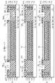
図2は、本実施形態の半導体ウェハーのスクライブ領域2における構造を示す平面図である。以下の説明においては、XYZ直交座標系が用いられることがある。当該直交座標系においては、ガードリング11が延伸する方向(即ち、スクライブ領域2が延伸する方向)にY軸が規定され、ガードリング11が延伸する方向に垂直な方向(即ち、スクライブ領域2を横断する方向)にX軸が規定され、当該半導体ウェハーの厚さ方向にZ軸が規定される。 FIG. 2 is a plan view showing a structure in the
本実施形態の半導体ウェハーでは、回路形成領域1を取り囲むようにガードリング(シールリング)11が設けられる。ガードリング11は、半導体ICチップの端面からの水の侵入によるデバイスの動作特性の劣化のために設けられる構造体である。後述されるように、ガードリング11は、半導体ウェハーの厚さ方向に並んで配置された金属配線と、厚さ方向に隣接する金属配線を接続するコンタクトとを備えて構成される。ガードリング11を構成する各金属配線は、回路形成領域1の端に沿って延伸するように設けられる。本実施形態の半導体ウェハーでは、隣接するガードリング11(即ち、隣接する回路形成領域1のそれぞれに沿って設けられる2本のガードリング11)の間にスクライブ領域2が規定される。 In the semiconductor wafer of this embodiment, a guard ring (seal ring) 11 is provided so as to surround the
スクライブ領域2には、TEGが設けられる。本実施形態では、TEGパッド12と、テスト素子13と、TEGパッド12とテスト素子13とを接続する配線14とが、スクライブ領域2に設けられている。図2では、2端子素子であるテスト素子13が図示されているが、テスト素子13は、2端子素子に限られない。2端子素子以外の素子がテスト素子13に用いられる場合、テスト素子13に接続されるTEGパッド12、及び配線14の数も、適宜に変更される。 The
本実施形態の半導体ウェハーの表面には、ガードリング11に沿って溝部(スリット)15がエッチングによって形成されている。本実施形態では、溝部15が、ガードリング11とTEGパッド12の間を通過するように形成される。後に詳細に議論されるように、本実施形態の半導体ウェハーでは溝部15の平面形状が重要である。 Grooves (slits) 15 are formed by etching along the
図3は、本実施形態の半導体ウェハーのスクライブ領域2における構造を詳細に示す拡大平面図であり、図4A、図4Bは、本実施形態の半導体ウェハーの構造を示す断面図である。図4A(a)、(b)、(c)は、それぞれ、A−A断面、B−B断面、C−C断面における半導体ウェハーの構造を示しており、図4B(a)、(b)、(c)は、それぞれ、D−D断面、E−E断面、F−F断面における構造を示している。A−A断面、B−B断面、C−C断面、D−D断面、E−E断面、F−F断面は、いずれも、ガードリング11が延伸する方向(即ち、Y軸方向)に垂直な断面である。なお、図4A、図4Bは、発明の理解を容易にするために、本実施形態の半導体ウェハーの断面構造を概略的に示しており、構造の細部については、適宜に変更され得ることに留意されたい。 FIG. 3 is an enlarged plan view showing in detail the structure in the
図4A、図4Bに図示されているように、本実施形態の半導体ウェハーは、トランジスタその他の素子(図示されない)が形成された半導体基板21と、半導体基板21を被覆するように設けられた絶縁層22と、該絶縁層22を被覆するように形成された表面保護層(パッシベーション膜)23とを備えている。 As shown in FIGS. 4A and 4B, the semiconductor wafer of this embodiment includes a
ガードリング11は、絶縁層22の内部に形成された金属配線11a〜11eを備えている。金属配線11a〜11eは、半導体基板21の厚さ方向に並んで配置されている。 The
TEGパッド12は、隣接するガードリング11の間の位置に形成されている。TEGパッド12は、その外周の一部分が表面保護層23によって被覆されており、表面保護層23に形成された開口23aにおいて露出されている。なお、A−A断面、B−B断面、C−C断面の構造を示す図4Aにおいては、TEGパッド12が図示されているが、D−D断面、E−E断面、F−F断面の構造を示す図4Bにおいては、TEGパッド12に接続された配線14のみが図示されている。 The
加えて、TEGパッド12の下方に、金属配線16a〜16dが設けられている。金属配線16a〜16dは、半導体基板21の厚さ方向に並んで配置されている。 In addition, metal wirings 16 a to 16 d are provided below the
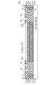
図5は、本実施形態の半導体ウェハーの構造を詳細に示す断面図である。なお、本実施形態の半導体ウェハーの構造の理解を容易にするために、図5においては、半導体ウェハーの構造の寸法(特に、半導体基板21の厚さ方向の寸法)が、実際の寸法に比例して図示されていないことに留意されたい。 FIG. 5 is a cross-sectional view showing in detail the structure of the semiconductor wafer of this embodiment. In order to facilitate understanding of the structure of the semiconductor wafer of the present embodiment, in FIG. 5, the dimensions of the structure of the semiconductor wafer (particularly the dimensions in the thickness direction of the semiconductor substrate 21) are proportional to the actual dimensions. Note that this is not shown.
半導体基板21の表側主面は、絶縁層22によって被覆されている。本実施形態では、絶縁層22は、この順に積層された、酸化シリコン膜31、炭窒化シリコン膜32、酸化シリコン膜33、炭窒化シリコン膜34、低誘電率膜35、炭窒化シリコン膜36、低誘電率膜37、炭窒化シリコン膜38、酸化シリコン膜39、炭窒化シリコン膜40、及び、酸化シリコン膜41を備えている。低誘電率膜35、37としては、例えば、比誘電率が3.3以下の有機シリカガラスで形成された絶縁膜が用いられる。 The front main surface of the
ガードリング11の金属配線11a、及び、TEGパッド12の下方に設けられた金属配線16aは、炭窒化シリコン膜32及び酸化シリコン膜33に形成された溝に埋め込まれ、金属配線11b及び金属配線16bは、低誘電率膜35に形成された溝に埋め込まれている。また、金属配線11c及び金属配線16cは、低誘電率膜37に形成された溝に埋め込まれており、金属配線11d及び金属配線16dは、酸化シリコン膜39に形成された溝に埋め込まれている。また、金属配線11e及びTEGパッド12は、酸化シリコン膜41の上に形成されている。金属配線11aは、酸化シリコン膜31を貫通するビアコンタクト51によって半導体基板21の拡散層(図示されない)に接合されており、金属配線11bは、低誘電率膜35及び炭窒化シリコン膜34を貫通するビアコンタクト52によって金属配線11aに接合されている。同様に、金属配線11cは、低誘電率膜37及び炭窒化シリコン膜36を貫通するビアコンタクト53によって金属配線11bに接合されており、金属配線11dは、酸化シリコン膜39及び炭窒化シリコン膜38を貫通するビアコンタクト54によって金属配線11cに接合されている。一実施形態では、金属配線11a〜11d、及び、金属配線16a〜16dとしては、銅配線が用いられ、金属配線11e及びTEGパッド12には、アルミニウム合金が用いられる。The
表面保護層23は、この順に積層された、酸化シリコン膜42及び窒化シリコン膜43を備えている。酸化シリコン膜42及び窒化シリコン膜43は、ガードリング11の金属配線11eを被覆するように形成され、更に、TEGパッド12を部分的に被覆するように形成されている。酸化シリコン膜42及び窒化シリコン膜43には、開口23aが形成され、TEGパッド12は、開口23aの内部において、露出されている。 The surface
溝部15は、ガードリング11とTEGパッド12との間の位置に形成されている。溝部15は、その深さ方向において、少なくとも表面保護層23を貫通するように形成されている。本実施形態では、溝部15は、深さ方向において、酸化シリコン膜39の途中の位置に到達するように形成されている。溝部15が、低誘電率膜35、37に到達していないことに留意されたい。これは、低誘電率膜35、37と比べてヤング率が高い材料である酸化シリコン膜39、41、42及び窒化シリコン膜43に選択的に溝部15を設けることで、クラックを抑制するためである。 The
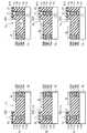
なお、図5には、A−A断面における半導体ウェハーの構造が図示されているが、B−B断面、C−C断面における半導体ウェハーの構造は、溝部15のX方向における幅が異なる以外は、A−A断面における半導体ウェハーの構造と同一である。また、D−D断面、E−E断面、及び、F−F断面における半導体ウェハーの構造は、TEGパッド12及び金属配線16a〜16bの代わりに配線14が存在する点以外は、それぞれ、A−A断面、B−B断面及びC−C断面における半導体ウェハーの構造と同一である。 FIG. 5 shows the structure of the semiconductor wafer in the AA cross section, but the structure of the semiconductor wafer in the BB cross section and the CC cross section is different except that the width of the
図3を再度に参照して、本実施形態の半導体ウェハーの構造においては、溝部15の平面形状が重要である。重要な点は、Y軸方向(ガードリング11が延伸する方向)に垂直で、且つ、TEGパッド12を通過する断面に関し、TEGパッド12と溝部15との距離が近い断面(具体的には、A−A断面)とTEGパッド12と溝部15との距離が遠い断面(具体的には、B−B断面)とが存在するということである。後に詳細に議論するように、TEGパッド12と溝部15との距離が近い断面の存在は、TEGパッド12のX軸方向の幅よりも薄いダイシングブレードを用いてダイシングをしても、TEGパッド12を除去することを可能にする。これは、スクライブ領域2の幅を狭くすることに寄与する。一方、TEGパッド12と溝部15との距離が遠い断面の存在は、チッピングの抑制に有効である。 Referring to FIG. 3 again, the planar shape of the
図6は、溝部15の平面形状を詳細に示す平面図である。図6(及び図3)に示されているように、溝部15のガードリング11に近い側面15dは、YZ平面に平行な面であり、Y軸方向に延伸するように形成されている。一方、溝部15のTEGパッド12に近い側面は、階段状に形成されている。詳細には、溝部15のTEGパッド12に沿った側面は、YZ平面に平行な面15a、15b、15cと、XZ平面に平行な面15e、15fとで構成されている。面15eは、X軸方向に延伸して面15a、15cを接続し、面15fは、X軸方向に延伸して面15b、15cを接続する。ここで、図6において、D1は、溝部15の面15aとTEGパッド12の間の距離を示しており、D2は、溝部15の面15bとTEGパッド12の間の距離を示しており、D3は、溝部15の面15cとTEGパッド12の間の距離を示している。図6の構造では、A−A断面においてはTEGパッド12と溝部15との距離D1が近く、B−B断面においてはTEGパッド12と溝部15との距離D2が遠い。また、C−C断面においては、TEGパッド12と溝部15との距離D3は、距離D1よりも遠く、距離D2よりも近い。FIG. 6 is a plan view showing in detail the planar shape of the
本実施形態では、溝部15は、Y軸方向において周期的な形状に形成されている。即ち、溝部15のTEGパッド12に沿った側面は、面15b、15f、15d、15e、15a、15e、15c、15fで構成される面を一の空間周期PSとして、Y軸方向に周期的な形状を有している。In the present embodiment, the
以上に説明されているような本実施形態の溝部15の平面形状は、チッピングを抑制すると共に、且つ、TEGパッド12のX軸方向の幅よりも薄いダイシングブレードを用いてダイシングを行うことを可能にする点で有用である。以下、本実施形態の溝部15の平面形状の有用性について議論する。図7は、図3の仮想線17の間の位置にダイシングブレードを接触させてダイシングが行われた場合の当該半導体ウェハーの状態を示す断面図である。 The planar shape of the
本実施形態の半導体ウェハーの一つの特徴は、TEGパッド12のX軸方向の幅よりも多少薄い厚さのダイシングブレード50を用いてダイシングを行っても、TEGパッド12を除去できることである。図7においては、TEGパッド12のX軸方向の幅よりも薄いダイシングブレード50が図示されていることに留意されたい。 One feature of the semiconductor wafer of this embodiment is that the
TEGパッド12のX軸方向の幅よりも薄いダイシングブレード50が用いられた場合、TEGパッド12に、ダイシングブレード50とは直接的に接触しない部分(以下、「非接触部分」という)が残存することになる。 When the
ただし、TEGパッド12の非接触部分には、ダイシングブレード50により、当該非接触部分を引きはがすような応力が作用する。本実施形態の半導体ウェハーでは、この応力を利用して、TEGパッド12の全体を除去することができる。詳細には、図7(a)に図示されているように、本実施形態の半導体ウェハーでは、TEGパッド12と溝部15との間の距離が近い断面(本実施形態では、A−A断面)においてダイシングブレード50と溝部15の距離d1が近くなる。よって、TEGパッド12の非接触部分を引きはがすような応力が作用したとき、該応力は、溝部15のTEGパッド12と溝部15との間の距離が近い位置において開放されやすい。言い換えれば、表面保護層23の溝部15の面15aとTEGパッド12の間の部分は、ダイシングブレード50によって非接触部分を引きはがすような応力が作用することによって破壊されやすい。したがって、TEGパッド12においてダイシングブレード50とは直接的に接触しない非接触部分があっても、当該非接触部分は、表面保護層23の溝部15の面15aとTEGパッド12の間の部分と共に除去することができる。However, the non-contact portion of the
このように、本実施形態の半導体ウェハーの構造によれば、TEGパッド12のX軸方向の幅よりも薄いダイシングブレード50を使用してダイシングを行うことができる。これは、スクライブ領域2の幅を狭くすることを可能にする。スクライブ領域2の幅は、用いられるダイシングブレード50の厚さと、ガードリング11とダイシングブレード50との間で確保すべき距離の和で決まる。ダイシングの際には、最終的に取得しようとする半導体ICチップへの損傷を防ぐために、ガードリング11とダイシングブレード50との間の距離を一定程度確保することが必要になることに留意されたい。本実施形態の半導体ウェハーの構造を用いることにより、薄いダイシングブレード50を使用することが可能になり、結果として、スクライブ領域2の幅を狭くすることできる。 Thus, according to the structure of the semiconductor wafer of this embodiment, dicing can be performed using the
一方、図7(b)に図示されているように、TEGパッド12と溝部15との間の距離が遠いB−B断面においては、ダイシングブレード50と溝部15の距離d2が遠くなり、これは、表面チッピングの抑制に寄与する。ダイシングブレード50が半導体ウェハーと接触したときには、半導体基板21の裏面の、ダイシングブレード50の厚さ方向の中心の位置の近傍においてクラックが発生する。当該クラックは、X軸方向(即ち、スクライブ領域2を横断する方向)に進行し、また、X軸方向に進行するにつれて、半導体ウェハーの表側主面に近づく。溝部15は、このクラックの進行を止める作用がある。そして、クラックの進行を止める作用は、溝部15とダイシングブレード50との間の距離が遠いほど効果的に得ることができる。よって、TEGパッド12と溝部15との間の距離が遠い断面(本実施形態では、B−B断面)が存在することにより、表面チッピングを抑制することができる。On the other hand, as illustrated in FIG. 7 (b), in the distance is long section B-B between the
また、TEGパッド12と溝部15との間の距離が中間的であるC−C断面の存在は、A−A断面において発生した表面保護層23の溝部15の面15aとTEGパッド12の間の部分の破壊を、B−B断面に伝搬させることに有効である。A−A断面とB−B断面の間に、TEGパッド12と溝部15との間の距離が中間的であるC−C断面を設けることで、TEGパッド12の除去の確実性を向上させることができる。 In addition, the presence of the CC cross section in which the distance between the
図8は、TEGパッド12のX軸方向の幅よりも薄いダイシングブレード50を使用してダイシングを行うことで得られる半導体ICチップの端部の構造を示す平面図であり、図9A、図9Bは、該半導体ICチップの端部の構造を示す断面図である。図8において、符号18は、ダイシングの切断面、即ち、半導体ICチップの端面を示しており、破線12aは、ダイシング前にTEGパッド12が存在していた位置を示している。 FIG. 8 is a plan view showing the structure of the end portion of the semiconductor IC chip obtained by dicing using a
TEGパッド12のX軸方向の幅よりも薄いダイシングブレード50を使用してダイシングが行われると、ダイシングの前にTEGパッド12が存在していた位置の近傍においてTEGパッド12を引きはがす応力が作用する。この応力によって表面保護層23が破壊されるとともにTEGパッド12が除去される。 When dicing is performed using a
得られた半導体ICチップは、A−A断面においては端面18と溝部15との距離d1が相対的に近く、B−B断面においては端面18と溝部15との距離d2が相対的に遠いような構造を有している。なお、C−C断面においては、端面18と溝部15との距離d3が、距離d1よりも遠く、距離d2よりも近い。The resulting semiconductor IC chips, A-A relatively close distanced 1 between the
なお、溝部15の端面18に近い側面は、ダイシングの際に破壊されることがある。図9Aは、溝部15の端面18に近い側面が、部分的に破壊された構造を図示している。しかしながら、ダイシングの際の破壊によって形成された面は、エッチングによって形成された溝部15の底面及び側面とは、構造的に区別できる。よって、実際の半導体ICチップにおいても、半導体ICチップの端面18と溝部15との距離を特定することができる。 In addition, the side surface close to the
また、図9Aに図示されているように、TEGパッド12の下方に位置していた金属配線16a〜16dのうち、切断面よりもガードリング11に近い部分は、ダイシングの後も半導体ICチップに残存する。金属配線16a〜16dの残存部の存在は、TEGパッド12のX軸方向の幅よりも薄いダイシングブレード50を使用してダイシングが行われたことを示す一つの根拠となり得る。 Further, as shown in FIG. 9A, portions of the
以上に説明されているように、本実施形態の半導体ウェハーの構造によれば、表面チッピングを抑制しつつ、スクライブ領域2の幅を狭くすることができる。 As described above, according to the structure of the semiconductor wafer of this embodiment, the width of the
なお、本実施形態において、Y軸方向に垂直で、且つ、TEGパッド12を通過する断面について、TEGパッド12と溝部15との距離が近い断面とTEGパッド12と溝部15との距離が遠い断面とが存在するという条件の下であれば、ガードリング11とTEGパッド12の間の通過するように設けられる溝部の形状は、様々に変更可能である。In the present embodiment, with respect to the cross section perpendicular to the Y-axis direction and passing through the
図10は、図3で図示されている形状の溝部15と異なる形状の溝部24を有する半導体ウェハーの構造を示す表面図である。図10に示されているように、溝部24のガードリング11に近い側面24dは、YZ平面に平行な面であり、Y軸方向に延伸するように形成されている。一方、溝部24のTEGパッド12に近い側面は、YZ平面に平行な面24a、24bと、XZ平面に平行な面24cとで構成されている。面24cは、X軸方向に延伸して面24a、24bを接続する。ここで、図10において、D1は、溝部24の面24aとTEGパッド12の間の距離を示しており、D2は、溝部24の面24bとTEGパッド12の間の距離を示している。図10の構造では、A−A断面においてはTEGパッド12と溝部24との距離D1が近く、B−B断面においてはTEGパッド12と溝部24との距離D2が遠い。FIG. 10 is a surface view showing a structure of a semiconductor wafer having a groove portion 24 having a shape different from the
このような構造においても、表面チッピングを抑制しつつ、スクライブ領域2の幅を狭くすることができる。即ち、TEGパッド12と溝部24との距離が近い断面(A−A断面)の存在は、TEGパッド12のX軸方向の幅よりも薄いダイシングブレードを用いてダイシングをしても、TEGパッド12を除去することを可能にする。これは、スクライブ領域2の幅を狭くすることに寄与する。一方、TEGパッド12と溝部24との距離が遠い断面(B−B断面)の存在は、チッピングの抑制に有効である。 Even in such a structure, the width of the
なお、溝部の平面形状は、図3、図10に図示されているものに限定されない。例えば、図10では、面24a、24bを接続する面24cは、面24a、24bに対して垂直であるが、面24cが面24a、24bに対して斜めに(例えば、45度をなす角度で)形成されてもよい。 Note that the planar shape of the groove is not limited to that illustrated in FIGS. 3 and 10. For example, in FIG. 10, the surface 24c connecting the
(第2の実施形態)
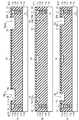
図11は、第2の実施形態の半導体ウェハーのスクライブ領域2における構造を詳細に示す拡大平面図であり、図12は、図11のA−A断面における半導体ウェハーの構造を示す断面図である。なお、A−A断面は、ガードリング11が延伸する方向(即ち、Y軸方向)に垂直な断面である。(Second Embodiment)
FIG. 11 is an enlarged plan view showing in detail the structure in the
図11及び図12に図示されているように、本実施形態の半導体ウェハーの構造は、第1の実施形態の半導体ウェハーの構造とほぼ同様であるが、ガードリング11に沿って、ガードリング11とTEGパッド12の間を通過するように2本の溝部25、26が設けられる点で相違する。溝部25、26は、いずれも、Y軸方向に延伸するように設けられる。ここで、溝部25は、ガードリング11に沿って設けられ、溝部26は、溝部25とTEGパッド12の間に、溝部25に沿って設けられる。溝部25の側壁25a、25bは、いずれも、YZ平面に平行であり、溝部26の側壁26a、26bは、いずれも、YZ平面に平行である。 As shown in FIGS. 11 and 12, the structure of the semiconductor wafer of this embodiment is substantially the same as the structure of the semiconductor wafer of the first embodiment, but along the
図13は、本実施形態の半導体ウェハーの構造を詳細に示す断面図である。溝部25、26は、その深さ方向において、少なくとも表面保護層23(即ち、酸化シリコン膜42及び窒化シリコン膜43)を貫通するように形成されている。本実施形態では、溝部25、26は、表面保護層23を貫通し、深さ方向において、酸化シリコン膜39の途中の位置に到達するように形成されている。 FIG. 13 is a cross-sectional view showing in detail the structure of the semiconductor wafer of this embodiment. The
このような構造においても、表面チッピングを抑制しつつ、スクライブ領域2の幅を狭くすることができる。即ち、TEGパッド12からの距離が近い溝部26が存在することにより、TEGパッド12のX軸方向の幅よりも薄いダイシングブレードを用いてダイシングをしても、TEGパッド12を除去することが可能になる。 Even in such a structure, the width of the
詳細には、第1の実施形態においても説明されているように、TEGパッド12のX軸方向の幅よりも薄いダイシングブレードが用いられた場合、TEGパッド12に、ダイシングブレードとは直接的に接触しない部分(以下、「非接触部分」という)が残存することになる。ただし、上述されているように、TEGパッド12の非接触部分には、ダイシングブレードにより、当該非接触部分を引きはがすような応力が作用するので、本実施形態の半導体ウェハーにおいても、この応力を利用して、TEGパッド12の全体を除去することができる。TEGパッド12からの距離が近い溝部26が設けられている本実施形態の半導体ウェハーでは、TEGパッド12の非接触部分を引きはがすような応力が作用したとき、該応力は、溝部26において開放されやすい。言い換えれば、絶縁層22及び表面保護層23の溝部26の側壁26aとTEGパッド12の間の部分は、ダイシングブレードによって非接触部分を引きはがすような応力が作用することによって破壊されやすい。したがって、TEGパッド12においてダイシングブレードとは直接的に接触しない非接触部分があっても、当該非接触部分は、絶縁層22及び表面保護層23の溝部26の側壁26aとTEGパッド12の間の部分と共に除去することができる。 Specifically, as described in the first embodiment, when a dicing blade thinner than the width of the
このように、本実施形態の半導体ウェハーの構造によれば、TEGパッド12のX軸方向の幅よりも薄いダイシングブレード50を使用してダイシングを行うことができる。これは、スクライブ領域2の幅を狭くすることを可能にする。 Thus, according to the structure of the semiconductor wafer of this embodiment, dicing can be performed using the
一方、TEGパッド12からの距離が遠い溝部25が設けられていることは、表面チッピングの抑制に寄与する。溝部25は、TEGパッド12からの距離が遠く、よって、ダイシングの際におけるダイシングブレードと溝部25の間の距離も遠くなる。これは、溝部25が、ダイシングブレードが半導体ウェハーと接触したときに発生するクラックの進行を止める作用が強いことを意味している。よって、TEGパッド12からの距離が遠い溝部25が設けられていることにより、表面チッピングを抑制することができる。 On the other hand, the provision of the
図14は、図11の仮想線27の間の位置にダイシングブレードを接触させてダイシングが行われた場合の行うことで得られる半導体ICチップの端部の構造を示す平面図であり、図15は、該半導体ICチップの端部の構造を示す断面図である。本実施形態においても、TEGパッド12のX軸方向の幅よりも薄いダイシングブレード50を使用してダイシングが行われる。図14において、符号28は、ダイシングの切断面、即ち、半導体ICチップの端面を示しており、破線12aは、ダイシング前にTEGパッド12が存在していた位置を示している。 14 is a plan view showing the structure of the end portion of the semiconductor IC chip obtained when dicing is performed by bringing a dicing blade into contact with the position between the
TEGパッド12のX軸方向の幅よりも薄いダイシングブレード50を使用してダイシングが行われると、ダイシングの前にTEGパッド12が存在していた位置の近傍において、TEGパッド12を引きはがす応力が作用する。この応力により、TEGパッド12が存在していた位置の近傍において表面保護層23が破壊されるとともにTEGパッド12が除去される。 When dicing is performed using a
得られた半導体ICチップにおいては、溝部26の半導体ICチップの端面28に近い側面は、ダイシングの際に破壊されることがある。図15は、溝部26の端面28に近い側面が、部分的に破壊された構造を図示している。しかしながら、ダイシングの際の破壊によって形成された面は、エッチングによって形成された溝部26の底面及び側面とは、構造的に区別できる。よって、実際の半導体ICチップにおいても、溝部26の存在を特定することができる。
In the obtained semiconductor IC chip, the side surface of the
また、図15に図示されているように、TEGパッド12の下方に位置していた金属配線16a〜16dのうち、切断面よりもガードリング11に近い部分は、ダイシングの後も残存する。金属配線16a〜16dの残存部の存在は、TEGパッド12のX軸方向の幅よりも薄いダイシングブレード50を使用してダイシングが行われたことを示す一つの根拠となり得る。 As shown in FIG. 15, portions of the metal wirings 16 a to 16 d located below the
以上に説明されているように、ガードリング11とTEGパッド12との間に2本の溝部25、26が設けられている本実施形態の半導体ウェハーの構造においても、表面チッピングを抑制しつつ、スクライブ領域2の幅を狭くすることができる。 As described above, even in the structure of the semiconductor wafer of this embodiment in which the two
以上、本発明者によってなされた発明を実施の形態に基づき具体的に説明したが、本発明は前記実施の形態に限定されるものではなく、その要旨を逸脱しない範囲で種々変更可能であることはいうまでもない。 As mentioned above, the invention made by the present inventor has been specifically described based on the embodiment. However, the present invention is not limited to the embodiment, and various modifications can be made without departing from the scope of the invention. Needless to say.
1 :回路形成領域
2 :スクライブ領域
11 :ガードリング
11a〜11e:金属配線
12 :TEGパッド
12a :破線
13 :テスト素子
14 :配線
15 :溝部
15a〜15c:面
15d :側面
15e、15f:面
16a〜16d:金属配線
17 :仮想線
18 :端面
21 :半導体基板
22 :絶縁層
23 :表面保護層
23a :開口
24 :溝部
24a〜24c:面
24d :側面
25 :溝部
25a :側壁
26 :溝部
26a :側壁
27 :仮想線
28 :端面
31 :酸化シリコン膜
32 :炭窒化シリコン膜
33 :酸化シリコン膜
34 :炭窒化シリコン膜
35 :低誘電率膜
36 :炭窒化シリコン膜
37 :低誘電率膜
38 :炭窒化シリコン膜
39 :酸化シリコン膜
40 :炭窒化シリコン膜
41 :酸化シリコン膜
42 :酸化シリコン膜
43 :窒化シリコン膜
50 :ダイシングブレード
51〜54:ビアコンタクト1: Circuit forming region 2: Scribe region 11: Guard rings 11a to 11e: Metal wiring 12:
Claims (4)
Translated fromJapanese前記回路形成領域のそれぞれを取り囲むように設けられたガードリングと、
隣接する前記ガードリングの間に設けられたスクライブ領域と、
前記スクライブ領域に設けられた素子と、
前記スクライブ領域に設けられ、前記素子に電気的に接続されたパッドと、
前記半導体ウェハーの表面に、前記ガードリングに沿って設けられた溝部
とを具備し、
前記溝部は、前記パッドと前記ガードリングの間を通過し、前記ガードリングが延伸する延伸方向に延伸するように設けられており、
前記溝部は、
第1側面と、
前記第1側面に対向し、前記パッドに前記第1側面よりも近い第2側面
とを有し、
前記第2側面は、
前記延伸方向と前記半導体ウェハーの厚さ方向とを含む平面に平行な第1面と、
前記平面に平行で、前記第1面から前記延伸方向にずれて位置する第2面と、
前記平面に平行で、前記第2面から前記延伸方向にずれて位置する第3面と、
前記平面に垂直で、前記第1面と前記第2面とを連結する第4面と、
前記平面に垂直で、前記第2面と前記第3面とを連結する第5面
とを有し、
前記第2面と前記パッドとの間の距離である第2距離が、前記第1面と前記パッドとの間の距離である第1距離よりも遠く、
前記第3面と前記パッドとの間の距離である第3距離が、前記第2距離よりも遠い
半導体ウェハー。A semiconductor wafer comprising a plurality of circuit formation regions on which integrated circuits are formed,
A guard ring provided so as to surround each of the circuit formation regions;
A scribe area provided between the adjacent guard rings;
An element provided in the scribe region;
A pad provided in the scribe region and electrically connected to the element;
The surface of the semiconductor wafer comprises a groove provided along the guard ring,
The groove portion is provided so as to pass between the pad and the guard ring andextend in an extending direction in which the guard ring extends ,
The groove is
A first aspect;
A second side surface facing the first side surface and closer to the pad than the first side surface
And
The second side surface is
A first surface parallel to a plane including the stretching direction and the thickness direction of the semiconductor wafer;
A second surface that is parallel to the plane and is offset from the first surface in the stretching direction;
A third surface that is parallel to the plane and is offset from the second surface in the stretching direction;
A fourth surface perpendicular to the plane and connecting the first surface and the second surface;
A fifth surface that is perpendicular to the plane and connects the second surface and the third surface.
And
A second distance that is a distance between the second surface and the pad is longer than a first distance that is a distance between the first surface and the pad;
A semiconductor wafer, wherein a third distance, which is a distance between the third surface and the pad, is farther than the second distance .
前記溝部が、前記延伸方向において周期的な形状に形成されている
半導体ウェハー。The semiconductor wafer accordingto claim 1,
A semiconductor wafer in which the groove is formed in a periodic shape in the stretching direction.
ダイシングブレードを用いて前記半導体ウェハーのダイシングを行って半導体ICチップを得る工程
とを具備し、
前記ダイシングブレードの厚さが、前記延伸方向と垂直な方向における前記パッドの幅よりも薄い
半導体ICチップの製造方法。Preparing a semiconductor wafer according to claim 1or 2 ,
And a step of dicing the semiconductor wafer using a dicing blade to obtain a semiconductor IC chip,
A method of manufacturing a semiconductor IC chip, wherein the thickness of the dicing blade is thinner than the width of the pad in a direction perpendicular to the extending direction.
前記回路形成領域のそれぞれを取り囲むように設けられたガードリング
とを備える半導体ICチップであって、
当該半導体ICチップの表面には、前記半導体ICチップの端面と前記ガードリングの間を通過するように前記ガードリングに沿って設けられた溝部が形成され、
前記溝部は、
第1側面と、
前記第1側面に対向し、前記半導体ICチップの前記端面に前記第1側面よりも近い第2側面
とを有し、
前記第2側面は、
前記ガードリングが延伸する延伸方向と前記半導体ウェハーの厚さ方向とを含む平面に平行な第1面と、
前記平面に平行で、前記第1面から前記延伸方向にずれて位置する第2面と、
前記平面に平行で、前記第2面から前記延伸方向にずれて位置する第3面と、
前記平面に垂直で、前記第1面と前記第2面とを連結する第4面と、
前記平面に垂直で、前記第2面と前記第3面とを連結する第5面
とを有し、
前記第2面と前記半導体ICチップの前記端面との間の距離である第2距離が、前記第1面と前記半導体ICチップの前記端面との間の距離である第1距離よりも遠く、
前記第3面と前記半導体ICチップの前記端面との間の距離である第3距離が、前記第2距離よりも遠い
半導体ICチップ。A circuit formation region in which an integrated circuit is formed;
A semiconductor IC chip comprising a guard ring provided so as to surround each of the circuit formation regions,
On the surface of the semiconductor IC chip, there is formed a groove provided along the guard ring so as to pass between the end face of the semiconductor IC chip and the guard ring,
The groove is
A first aspect;
A second side surface facing the first side surface and closer to the end surface of the semiconductor IC chip than the first side surface
And
The second side surface is
A first surface parallel to a plane including a stretching direction in which the guard ring extends and a thickness direction of the semiconductor wafer;
A second surface that is parallel to the plane and is offset from the first surface in the stretching direction;
A third surface that is parallel to the plane and is offset from the second surface in the stretching direction;
A fourth surface perpendicular to the plane and connecting the first surface and the second surface;
A fifth surface that is perpendicular to the plane and connects the second surface and the third surface.
And
A second distance that is a distance between the second surface and the end surface of the semiconductor IC chip is farther than a first distance that is a distance between the first surface and the end surface of the semiconductor IC chip;
A semiconductor IC chip, wherein a third distance, which is a distance between the third surface and the end surface of the semiconductor IC chip, is longer than the second distance .
Priority Applications (3)
| Application Number | Priority Date | Filing Date | Title |
|---|---|---|---|
| JP2013149392AJP6234725B2 (en) | 2013-07-18 | 2013-07-18 | Semiconductor wafer, semiconductor IC chip and manufacturing method thereof |
| US14/329,816US9443808B2 (en) | 2013-07-18 | 2014-07-11 | Semiconductor wafer, semiconductor IC chip and manufacturing method of the same |
| CN201410344850.3ACN104299898B (en) | 2013-07-18 | 2014-07-18 | Semiconductor wafer, semiconductor IC chip and its manufacturing method |
Applications Claiming Priority (1)
| Application Number | Priority Date | Filing Date | Title |
|---|---|---|---|
| JP2013149392AJP6234725B2 (en) | 2013-07-18 | 2013-07-18 | Semiconductor wafer, semiconductor IC chip and manufacturing method thereof |
Publications (2)
| Publication Number | Publication Date |
|---|---|
| JP2015023121A JP2015023121A (en) | 2015-02-02 |
| JP6234725B2true JP6234725B2 (en) | 2017-11-22 |
Family
ID=52319574
Family Applications (1)
| Application Number | Title | Priority Date | Filing Date |
|---|---|---|---|
| JP2013149392AExpired - Fee RelatedJP6234725B2 (en) | 2013-07-18 | 2013-07-18 | Semiconductor wafer, semiconductor IC chip and manufacturing method thereof |
Country Status (3)
| Country | Link |
|---|---|
| US (1) | US9443808B2 (en) |
| JP (1) | JP6234725B2 (en) |
| CN (1) | CN104299898B (en) |
Families Citing this family (10)
| Publication number | Priority date | Publication date | Assignee | Title |
|---|---|---|---|---|
| US9831193B1 (en)* | 2016-05-31 | 2017-11-28 | Texas Instruments Incorporated | Methods and apparatus for scribe street probe pads with reduced die chipping during wafer dicing |
| US9905466B2 (en)* | 2016-06-28 | 2018-02-27 | Taiwan Semiconductor Manufacturing Company, Ltd. | Wafer partitioning method and device formed |
| KR102633112B1 (en) | 2016-08-05 | 2024-02-06 | 삼성전자주식회사 | Semiconductor device |
| KR102428328B1 (en)* | 2017-07-26 | 2022-08-03 | 삼성전자주식회사 | Semiconductor device |
| KR102497570B1 (en) | 2018-01-18 | 2023-02-10 | 삼성전자주식회사 | Semiconductor device |
| EP3557610A1 (en) | 2018-04-17 | 2019-10-23 | Infineon Technologies Austria AG | Semiconductor wafer, semiconductor chip and method of fabricating a semiconductor wafer |
| CN113130413B (en)* | 2019-12-30 | 2024-09-06 | 联华电子股份有限公司 | Semiconductor element packaging structure and manufacturing method thereof |
| TWI791209B (en)* | 2020-04-29 | 2023-02-01 | 台灣積體電路製造股份有限公司 | Semiconductor die and method for forming an integrated fan-out structure |
| CN116417402A (en)* | 2022-01-10 | 2023-07-11 | 意法半导体(克洛尔2)公司 | Method for manufacturing integrated circuit from semiconductor substrate wafer |
| JP2023105428A (en)* | 2022-01-19 | 2023-07-31 | キヤノントッキ株式会社 | SUBSTRATE HOLDING DEVICE, ELECTROSTATIC CHUCK, AND SUBSTRATE HOLDING METHOD |
Family Cites Families (8)
| Publication number | Priority date | Publication date | Assignee | Title |
|---|---|---|---|---|
| JPH06275713A (en)* | 1993-03-19 | 1994-09-30 | Hitachi Ltd | Semiconductor wafer, semiconductor chip, and dicing method |
| JP2003257895A (en)* | 2002-02-28 | 2003-09-12 | Mitsubishi Electric Corp | Wafer on which semiconductor chip is mounted and method of manufacturing the same |
| JP2004055852A (en)* | 2002-07-19 | 2004-02-19 | Ricoh Co Ltd | Semiconductor device and manufacturing method thereof |
| JP2006108489A (en)* | 2004-10-07 | 2006-04-20 | Toshiba Corp | Manufacturing method of semiconductor device |
| JP2006140404A (en) | 2004-11-15 | 2006-06-01 | Renesas Technology Corp | Semiconductor device |
| JP2007049066A (en)* | 2005-08-12 | 2007-02-22 | Seiko Epson Corp | Semiconductor wafer, semiconductor chip and manufacturing method thereof |
| JP2011014605A (en)* | 2009-06-30 | 2011-01-20 | Sanyo Electric Co Ltd | Semiconductor apparatus and method of manufacturing the same |
| JP5953974B2 (en)* | 2011-09-15 | 2016-07-20 | 富士通セミコンダクター株式会社 | Semiconductor device and manufacturing method of semiconductor device |
- 2013
- 2013-07-18JPJP2013149392Apatent/JP6234725B2/ennot_activeExpired - Fee Related
- 2014
- 2014-07-11USUS14/329,816patent/US9443808B2/ennot_activeExpired - Fee Related
- 2014-07-18CNCN201410344850.3Apatent/CN104299898B/enactiveActive
Also Published As
| Publication number | Publication date |
|---|---|
| US20150021733A1 (en) | 2015-01-22 |
| CN104299898A (en) | 2015-01-21 |
| CN104299898B (en) | 2018-11-30 |
| US9443808B2 (en) | 2016-09-13 |
| JP2015023121A (en) | 2015-02-02 |
Similar Documents
| Publication | Publication Date | Title |
|---|---|---|
| JP6234725B2 (en) | Semiconductor wafer, semiconductor IC chip and manufacturing method thereof | |
| JP5173525B2 (en) | Semiconductor wafer, semiconductor chip, semiconductor device, and manufacturing method of semiconductor device | |
| JP6061726B2 (en) | Semiconductor device and semiconductor wafer | |
| US8125053B2 (en) | Embedded scribe lane crack arrest structure for improved IC package reliability of plastic flip chip devices | |
| TWI709183B (en) | Semiconductor test structure and method for forming the same | |
| US8994148B2 (en) | Device bond pads over process control monitor structures in a semiconductor die | |
| US20070029641A1 (en) | Semiconductor device | |
| JP2009290090A (en) | Semiconductor device and method for manufacturing the same | |
| JP2006140404A (en) | Semiconductor device | |
| CN101419948A (en) | Semiconductor device and method for fabricating the same | |
| US20120286397A1 (en) | Die Seal for Integrated Circuit Device | |
| CN106935556A (en) | Semiconductor package assembly and a manufacturing method thereof | |
| US9318461B2 (en) | Wafer level array of chips and method thereof | |
| JP2010225648A (en) | Semiconductor device and manufacturing method thereof | |
| JP2017168732A (en) | Semiconductor device | |
| US9275963B2 (en) | Semiconductor structure having stage difference surface and manufacturing method thereof | |
| CN102263076B (en) | Package structure and method for forming package structure | |
| TWI473220B (en) | Semiconductor stacked structure and method of fabricating the same | |
| JP2009076782A (en) | Semiconductor substrate, manufacturing method thereof, and semiconductor chip | |
| KR20130011386A (en) | Semiconductor device and method for forming the same | |
| JP2011082434A (en) | Wafer and method of manufacturing semiconductor device | |
| CN100407403C (en) | semiconductor wafer | |
| JP5580458B2 (en) | Semiconductor device | |
| US7964960B2 (en) | Semiconductor device having non parallel cleavage planes in a substrate and supporting substrate | |
| JP2014220375A (en) | Semiconductor device and manufacturing method of the same |
Legal Events
| Date | Code | Title | Description |
|---|---|---|---|
| A621 | Written request for application examination | Free format text:JAPANESE INTERMEDIATE CODE: A621 Effective date:20160426 | |
| A977 | Report on retrieval | Free format text:JAPANESE INTERMEDIATE CODE: A971007 Effective date:20170216 | |
| A131 | Notification of reasons for refusal | Free format text:JAPANESE INTERMEDIATE CODE: A131 Effective date:20170222 | |
| A521 | Request for written amendment filed | Free format text:JAPANESE INTERMEDIATE CODE: A523 Effective date:20170418 | |
| TRDD | Decision of grant or rejection written | ||
| A01 | Written decision to grant a patent or to grant a registration (utility model) | Free format text:JAPANESE INTERMEDIATE CODE: A01 Effective date:20170927 | |
| A61 | First payment of annual fees (during grant procedure) | Free format text:JAPANESE INTERMEDIATE CODE: A61 Effective date:20171025 | |
| R150 | Certificate of patent or registration of utility model | Ref document number:6234725 Country of ref document:JP Free format text:JAPANESE INTERMEDIATE CODE: R150 | |
| LAPS | Cancellation because of no payment of annual fees |