JP6227082B1 - Connection module - Google Patents
Connection moduleDownload PDFInfo
- Publication number
- JP6227082B1 JP6227082B1JP2016195416AJP2016195416AJP6227082B1JP 6227082 B1JP6227082 B1JP 6227082B1JP 2016195416 AJP2016195416 AJP 2016195416AJP 2016195416 AJP2016195416 AJP 2016195416AJP 6227082 B1JP6227082 B1JP 6227082B1
- Authority
- JP
- Japan
- Prior art keywords
- protector
- substrate
- connection module
- horizontal
- power storage
- Prior art date
- Legal status (The legal status is an assumption and is not a legal conclusion. Google has not performed a legal analysis and makes no representation as to the accuracy of the status listed.)
- Active
Links
Images


Classifications
- H—ELECTRICITY
- H01—ELECTRIC ELEMENTS
- H01M—PROCESSES OR MEANS, e.g. BATTERIES, FOR THE DIRECT CONVERSION OF CHEMICAL ENERGY INTO ELECTRICAL ENERGY
- H01M50/00—Constructional details or processes of manufacture of the non-active parts of electrochemical cells other than fuel cells, e.g. hybrid cells
- H01M50/20—Mountings; Secondary casings or frames; Racks, modules or packs; Suspension devices; Shock absorbers; Transport or carrying devices; Holders
- H01M50/249—Mountings; Secondary casings or frames; Racks, modules or packs; Suspension devices; Shock absorbers; Transport or carrying devices; Holders specially adapted for aircraft or vehicles, e.g. cars or trains
- H—ELECTRICITY
- H01—ELECTRIC ELEMENTS
- H01M—PROCESSES OR MEANS, e.g. BATTERIES, FOR THE DIRECT CONVERSION OF CHEMICAL ENERGY INTO ELECTRICAL ENERGY
- H01M10/00—Secondary cells; Manufacture thereof
- H01M10/42—Methods or arrangements for servicing or maintenance of secondary cells or secondary half-cells
- H01M10/48—Accumulators combined with arrangements for measuring, testing or indicating the condition of cells, e.g. the level or density of the electrolyte
- H01M10/482—Accumulators combined with arrangements for measuring, testing or indicating the condition of cells, e.g. the level or density of the electrolyte for several batteries or cells simultaneously or sequentially
- H—ELECTRICITY
- H01—ELECTRIC ELEMENTS
- H01M—PROCESSES OR MEANS, e.g. BATTERIES, FOR THE DIRECT CONVERSION OF CHEMICAL ENERGY INTO ELECTRICAL ENERGY
- H01M50/00—Constructional details or processes of manufacture of the non-active parts of electrochemical cells other than fuel cells, e.g. hybrid cells
- H01M50/20—Mountings; Secondary casings or frames; Racks, modules or packs; Suspension devices; Shock absorbers; Transport or carrying devices; Holders
- H01M50/204—Racks, modules or packs for multiple batteries or multiple cells
- H01M50/207—Racks, modules or packs for multiple batteries or multiple cells characterised by their shape
- H01M50/209—Racks, modules or packs for multiple batteries or multiple cells characterised by their shape adapted for prismatic or rectangular cells
- H—ELECTRICITY
- H01—ELECTRIC ELEMENTS
- H01M—PROCESSES OR MEANS, e.g. BATTERIES, FOR THE DIRECT CONVERSION OF CHEMICAL ENERGY INTO ELECTRICAL ENERGY
- H01M50/00—Constructional details or processes of manufacture of the non-active parts of electrochemical cells other than fuel cells, e.g. hybrid cells
- H01M50/20—Mountings; Secondary casings or frames; Racks, modules or packs; Suspension devices; Shock absorbers; Transport or carrying devices; Holders
- H01M50/284—Mountings; Secondary casings or frames; Racks, modules or packs; Suspension devices; Shock absorbers; Transport or carrying devices; Holders with incorporated circuit boards, e.g. printed circuit boards [PCB]
- H—ELECTRICITY
- H01—ELECTRIC ELEMENTS
- H01M—PROCESSES OR MEANS, e.g. BATTERIES, FOR THE DIRECT CONVERSION OF CHEMICAL ENERGY INTO ELECTRICAL ENERGY
- H01M50/00—Constructional details or processes of manufacture of the non-active parts of electrochemical cells other than fuel cells, e.g. hybrid cells
- H01M50/50—Current conducting connections for cells or batteries
- H01M50/502—Interconnectors for connecting terminals of adjacent batteries; Interconnectors for connecting cells outside a battery casing
- H01M50/507—Interconnectors for connecting terminals of adjacent batteries; Interconnectors for connecting cells outside a battery casing comprising an arrangement of two or more busbars within a container structure, e.g. busbar modules
- H—ELECTRICITY
- H01—ELECTRIC ELEMENTS
- H01M—PROCESSES OR MEANS, e.g. BATTERIES, FOR THE DIRECT CONVERSION OF CHEMICAL ENERGY INTO ELECTRICAL ENERGY
- H01M50/00—Constructional details or processes of manufacture of the non-active parts of electrochemical cells other than fuel cells, e.g. hybrid cells
- H01M50/50—Current conducting connections for cells or batteries
- H01M50/502—Interconnectors for connecting terminals of adjacent batteries; Interconnectors for connecting cells outside a battery casing
- H01M50/519—Interconnectors for connecting terminals of adjacent batteries; Interconnectors for connecting cells outside a battery casing comprising printed circuit boards [PCB]
- H—ELECTRICITY
- H01—ELECTRIC ELEMENTS
- H01M—PROCESSES OR MEANS, e.g. BATTERIES, FOR THE DIRECT CONVERSION OF CHEMICAL ENERGY INTO ELECTRICAL ENERGY
- H01M2220/00—Batteries for particular applications
- H01M2220/20—Batteries in motive systems, e.g. vehicle, ship, plane
- H—ELECTRICITY
- H01—ELECTRIC ELEMENTS
- H01M—PROCESSES OR MEANS, e.g. BATTERIES, FOR THE DIRECT CONVERSION OF CHEMICAL ENERGY INTO ELECTRICAL ENERGY
- H01M50/00—Constructional details or processes of manufacture of the non-active parts of electrochemical cells other than fuel cells, e.g. hybrid cells
- H01M50/50—Current conducting connections for cells or batteries
- H01M50/502—Interconnectors for connecting terminals of adjacent batteries; Interconnectors for connecting cells outside a battery casing
- H01M50/514—Methods for interconnecting adjacent batteries or cells
- H01M50/517—Methods for interconnecting adjacent batteries or cells by fixing means, e.g. screws, rivets or bolts
- Y—GENERAL TAGGING OF NEW TECHNOLOGICAL DEVELOPMENTS; GENERAL TAGGING OF CROSS-SECTIONAL TECHNOLOGIES SPANNING OVER SEVERAL SECTIONS OF THE IPC; TECHNICAL SUBJECTS COVERED BY FORMER USPC CROSS-REFERENCE ART COLLECTIONS [XRACs] AND DIGESTS
- Y02—TECHNOLOGIES OR APPLICATIONS FOR MITIGATION OR ADAPTATION AGAINST CLIMATE CHANGE
- Y02E—REDUCTION OF GREENHOUSE GAS [GHG] EMISSIONS, RELATED TO ENERGY GENERATION, TRANSMISSION OR DISTRIBUTION
- Y02E60/00—Enabling technologies; Technologies with a potential or indirect contribution to GHG emissions mitigation
- Y02E60/10—Energy storage using batteries
Landscapes
- Chemical & Material Sciences (AREA)
- Chemical Kinetics & Catalysis (AREA)
- Electrochemistry (AREA)
- General Chemical & Material Sciences (AREA)
- Engineering & Computer Science (AREA)
- Aviation & Aerospace Engineering (AREA)
- Manufacturing & Machinery (AREA)
- Connection Of Batteries Or Terminals (AREA)
- Battery Mounting, Suspending (AREA)
Abstract
Translated fromJapaneseDescription
Translated fromJapanese本発明は、接続モジュールに関し、詳しくは、蓄電モジュールに使用される接続モジュールに関する。 The present invention relates to a connection module, and more particularly to a connection module used for a power storage module.
従来、正極及び負極の電極端子を備えた蓄電素子を複数並べた蓄電素子群の上面に取り付けられる接続モジュールとして、特許文献1に記載のものが知られている。この種の接続モジュールは、電気自動車やハイブリッド車等の車両に搭載された蓄電素子群に取り付けられる。 2. Description of the Related Art Conventionally, a connection module described in Patent Document 1 is known as a connection module that is attached to the upper surface of a power storage element group in which a plurality of power storage elements having positive and negative electrode terminals are arranged. This type of connection module is attached to a storage element group mounted on a vehicle such as an electric vehicle or a hybrid vehicle.
上記文献1の接続モジュール(電池配線モジュール)は、電極端子間を接続する複数のバスバーと、蓄電素子の状態を検出するための複数の導電路(検出線)が形成されたフレキシブルプリント基板と、これら複数のバスバーとフレキシブルプリント基板とを保持する絶縁プロテクタとを備えている。また、フレキシブルプリント基板に補強板を設けることによって、さらに蓄電素子に関する情報を処理するための電気回路を構成する電子部品のフレキシブルプリント基板への実装を可能としている。 The connection module (battery wiring module) of Document 1 includes a plurality of bus bars for connecting electrode terminals, a flexible printed circuit board on which a plurality of conductive paths (detection lines) for detecting the state of the storage element are formed, An insulation protector for holding the plurality of bus bars and the flexible printed circuit board is provided. Further, by providing a reinforcing plate on the flexible printed circuit board, it is possible to mount electronic components constituting an electric circuit for processing information on the power storage element on the flexible printed circuit board.
上記従来の接続モジュールでは、フレキシブルプリント基板に電子部品の実装を可能にすることによって、接続モジュールを一層小型化できる。しかしながら、蓄電素子群の高圧化等に伴い、蓄電素子群における蓄電素子の個数が増大するにつれて検出線の数が増大する。その場合、フレキシブルプリント基板の面積も増大する。また、蓄電素子群の上面には、排気用のダクト等が設けられる場合があり、その場合、蓄電素子群の上面上での接続モジュールの占有面積が制限される。そのため、蓄電素子数の増加に対応しつつ、蓄電素子群の上面上での接続モジュールの占有面積を縮小化できる接続モジュールが所望されていた。 In the conventional connection module, the connection module can be further reduced in size by enabling mounting of electronic components on the flexible printed circuit board. However, the number of detection lines increases as the number of power storage elements in the power storage element group increases as the pressure of the power storage element group increases. In that case, the area of the flexible printed circuit board also increases. In addition, an exhaust duct or the like may be provided on the upper surface of the power storage element group, and in that case, the area occupied by the connection module on the upper surface of the power storage element group is limited. Therefore, there has been a demand for a connection module that can reduce the area occupied by the connection module on the upper surface of the power storage element group while accommodating the increase in the number of power storage elements.
そこで、本明細書では、蓄電素子数の増加に対応しつつ、蓄電素子群の上面上での接続モジュールの占有面積を縮小化できる接続モジュールを提供する。 Therefore, the present specification provides a connection module that can reduce the occupied area of the connection module on the upper surface of the power storage element group while accommodating an increase in the number of power storage elements.
本明細書によって開示される接続モジュールは、正極及び負極の電極端子を有する複数の蓄電素子が並べられた蓄電素子群に取り付けられて前記電極端子間を接続する接続モジュールであって、前記電極端子間を接続する複数のバスバーを保持する絶縁プロテクタと、前記絶縁プロテクタに保持され、前記バスバーに接続され前記蓄電素子の状態を検出する検出線が形成されたフレキシブルプリント基板と、を備え、前記絶縁プロテクタは、前記バスバーを保持する保持部が一端側に形成されたプロテクタ水平部と、前記一端側に対向する前記プロテクタ水平部の他端側の少なくとも一部において、前記プロテクタ水平部から垂直方向に延びる垂直部と、を含み、前記フレキシブルプリント基板は、前記プロテクタ水平部に保持される基板水平部と、前記基板水平部に対して垂直に折り曲げられ、前記垂直部に保持される折り曲げ部と、を含む。
本構成によれば、絶縁プロテクタは、プロテクタ水平部の他端側の少なくとも一部において、プロテクタ水平部から垂直方向に延びる垂直部を含む。また、蓄電素子の状態を検出する検出線が形成されたフレキシブルプリント基板は、基板水平部に加え、絶縁プロテクタの垂直部に保持される折り曲げ部を含む。そのため、折り曲げ部によって、フレキシブルプリント基板の配線面積を減少させることなく、蓄電素子群上での占有面積を縮小化できる。また、折り曲げ部の面積を蓄電素子数に応じて変更することによって蓄電素子数の増加にも対応できる。すなわち、本構成によれば、蓄電素子数の増加に対応しつつ、蓄電素子群の上面上での接続モジュールの占有面積を縮小化できる。The connection module disclosed in this specification is a connection module that is attached to a storage element group in which a plurality of storage elements having positive and negative electrode terminals are arranged to connect the electrode terminals, and the electrode terminals An insulating protector that holds a plurality of bus bars that connect each other, and a flexible printed board that is held by the insulating protector and formed with a detection line that is connected to the bus bar and detects the state of the storage element. The protector includes a protector horizontal portion having a holding portion for holding the bus bar formed on one end side, and at least part of the other end side of the protector horizontal portion facing the one end side in a vertical direction from the protector horizontal portion. The flexible printed circuit board is held by the horizontal part of the protector. And parts bent perpendicular to the substrate horizontal part comprises a bent portion which is held in the vertical section.
According to this configuration, the insulating protector includes the vertical portion extending in the vertical direction from the protector horizontal portion at least at a part of the other end side of the protector horizontal portion. Moreover, the flexible printed circuit board on which the detection line for detecting the state of the power storage element is formed includes a bent portion that is held by the vertical portion of the insulating protector in addition to the horizontal portion of the substrate. Therefore, the area occupied on the power storage element group can be reduced without reducing the wiring area of the flexible printed circuit board by the bent portion. In addition, an increase in the number of power storage elements can be accommodated by changing the area of the bent portion according to the number of power storage elements. That is, according to this configuration, it is possible to reduce the occupation area of the connection module on the upper surface of the power storage element group while accommodating an increase in the number of power storage elements.
上記接続モジュールにおいて、前記絶縁プロテクタは、各バスバーに対応した複数のユニットプロテクタによって構成され、前記フレキシブルプリント基板は、各ユニットプロテクタに対応した複数のユニット基板によって構成され、隣接する二つのバスバーの間隙に対応した位置において、隣接する二つのユニットプロテクタのプロテクタ水平部間には、前記隣接する二つのプロテクタ水平部を連結するとともに、前記間隙よりも長い長さを有するプロテクタ余長部が形成されており、隣接する二つのユニット基板の基板水平部間には、前記隣接する二つの基板水平部を連結するとともに、前記間隙よりも長い長さを有する水平余長部が形成されており、隣接する二つのユニット基板の折り曲げ部間には、前記隣接する二つの折り曲げ部を連結するとともに、前記間隙よりも長い長さを有する垂直余長部が形成されているようにしてもよい。
本構成によれば、各連結部によって電極端子間のピッチ公差を吸収することができる。In the connection module, the insulation protector is configured by a plurality of unit protectors corresponding to each bus bar, and the flexible printed circuit board is configured by a plurality of unit substrates corresponding to each unit protector, and a gap between two adjacent bus bars. Between the protector horizontal portions of two adjacent unit protectors, the two adjacent protector horizontal portions are connected, and a protector extra length portion having a length longer than the gap is formed. In addition, between the two adjacent unit substrate horizontal portions, the two adjacent substrate horizontal portions are connected to each other, and a horizontal surplus portion having a length longer than the gap is formed. Between the two bent portions of the unit substrate, the two adjacent bent portions are arranged. As well as binding, it may be vertical excess length portion is formed to have a length longer than the gap.
According to this structure, the pitch tolerance between electrode terminals can be absorbed by each connection part.
また、上記接続モジュールにおいて、前記水平余長部と、前記垂直余長部との間には開口部が形成されているようにしてもよい。
本構成によれば、開口部の大きさを適宜設定することで、一枚のフレキシブルプリント基板から複数のユニット基板、水平余長部、および垂直余長部を、好適に形成することができる。In the connection module, an opening may be formed between the horizontal surplus length portion and the vertical surplus length portion.
According to this configuration, by appropriately setting the size of the opening, a plurality of unit substrates, horizontal surplus portions, and vertical surplus portions can be suitably formed from one flexible printed circuit board.
また、上記接続モジュールにおいて、前記絶縁プロテクタは、前記複数の蓄電素子の上面において、前記複数の蓄電素子の並び方向と垂直方向の一端部に取り付けられる第1プロテクタと、前記複数の蓄電素子の上面において、前記一端部と対向する他端部に取り付けられる第2プロテクタとを含み、前記フレキシブルプリント基板は、前記第1プロテクタに保持される第1基板と、第2プロテクタに保持される第2基板と、前記第1基板と前記第2基板とを電気的に接続する基板接続部と、を含み、前記第1プロテクタおよび前記第2プロテクタの一端部には、前記第1プロテクタと前記第2プロテクタとを一体化するとともに、前記基板接続部を載置する載置部が形成されており、前記第1プロテクタおよび前記第2プロテクタの他端部には、前記第1プロテクタと前記第2プロテクタとを結合する結合部が形成されているようにしてもよい。
本構成によれば、電極列が二列に構成される蓄電素子群に対応できるとともに、結合部によって第1プロテクタと第2プロテクタとが結合されているため、接続モジュールを蓄電素子群に取り付ける際の接続モジュールのハンドリングが向上する。それによって、接続モジュールの取り付け作業が効率化される。Further, in the connection module, the insulating protector includes a first protector attached to one end portion in a direction perpendicular to the arrangement direction of the plurality of power storage elements on the top surface of the plurality of power storage elements, and top surfaces of the plurality of power storage elements. A second protector attached to the other end opposite the one end, wherein the flexible printed circuit board is a first substrate held by the first protector and a second substrate held by the second protector. And a board connecting portion for electrically connecting the first board and the second board, and the first protector and the second protector are provided at one end of the first protector and the second protector. And the other end of the first protector and the second protector are formed. It may also be bonded portion for coupling the second protector and the first protector is formed.
According to this configuration, since the first protector and the second protector are coupled to each other by the coupling portion, the first protector and the second protector are coupled to each other, so that when the connection module is attached to the electrical storage element group. The handling of the connection module is improved. Thereby, the attachment work of the connection module is made efficient.
また、上記接続モジュールにおいて、前記第1基板および前記第2基板の少なくとも一方には、前記バスバーを介して取り込んだ前記蓄電素子に関する情報を処理するための電子部品が実装されているようにしてもよい。
本構成によれば、フレキシブルプリント基板に電子部品が実装されると、フレキシブルプリント基板内における検出線の配線スペースが減少することとなるが、折り曲げ部に検出線を配線することによって、フレキシブルプリント基板の平面面積を増加させることなく配線スペースの減少を補うことできる。そのため、フレキシブルプリント基板に電子部品が実装される本構成において、折り曲げ部をより有効に利用できる。In the connection module, at least one of the first substrate and the second substrate may be mounted with an electronic component for processing information relating to the storage element taken in via the bus bar. Good.
According to this configuration, when an electronic component is mounted on the flexible printed circuit board, the wiring space for the detection line in the flexible printed circuit board is reduced. By wiring the detection line to the bent portion, the flexible printed circuit board The reduction of the wiring space can be compensated for without increasing the plane area. Therefore, in the present configuration in which the electronic component is mounted on the flexible printed board, the bent portion can be used more effectively.
本発明の接続モジュールによれば、蓄電素子数の増加に対応しつつ、蓄電素子群の上面上での接続モジュールの占有面積を縮小化できる。 According to the connection module of the present invention, the area occupied by the connection module on the upper surface of the power storage element group can be reduced while accommodating the increase in the number of power storage elements.
<実施形態>
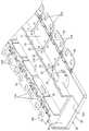
一実施形態を図1から図10を参照して説明する。本実施形態に係る蓄電モジュール10は、例えば、電気自動車またはハイブリッド自動車等の駆動源として使用される。蓄電モジュール10は、図1に示すように、複数(本実施形態では28個)の蓄電素子11が横並びに配置された蓄電素子群12と、蓄電素子群12に取り付けられて複数の蓄電素子11を接続する接続モジュール15とから構成されている。また、蓄電素子群12の上部中央部には、排気用のダクト13が設けられている。なお、図1において矢印Xで示される方向を蓄電モジュール10における左方向とし、矢印Yで示される方向を後方とし、矢印Zで示される方向を上方とする。<Embodiment>
One embodiment will be described with reference to FIGS. The
1.蓄電素子群
図1に示すように、蓄電素子11は、扁平な略直方体形状をなしており、その内部には図示しない発電要素が収容されている。蓄電素子11の上面には、前後方向の両端部寄りの位置に、一対の電極端子14が上方に突出して形成されている。一対の電極端子14の一方は正極端子14Aであり、他方は負極端子14Bである。電極端子14は、雄ねじ状に形成されている。各蓄電素子11の正負の向きは、互いに隣り合う蓄電素子11において逆向きになっており、これにより互いに異極の電極端子14が隣り合うように構成されている。この構成によって形成された電極列が、蓄電素子群12の上面においてダクト13を挟んで前後二列に配置されている。電極端子14は接続モジュール15に保持されたバスバー40を挟んでナット(図示せず)で締め付けられる。複数の蓄電素子11は、詳しくは図示しないが、保持板等の公知の固定手段により固定されている。1. Storage Element Group As shown in FIG. 1, the
2.接続モジュールの構成
図1に示すように、蓄電素子群12の上面には、蓄電素子11の並び方向(矢印X方向)に沿って細長い接続モジュール15が配置されている。
接続モジュール15は、大まかには、図2および図3に示されるように、電極端子14間を接続する複数のバスバー40を保持する絶縁プロテクタ30と、絶縁プロテクタ30に保持され、バスバー40に接続され蓄電素子11の状態を検出する検出線28(図9参照)が形成されたフレキシブルプリント基板(以下、単に「FPC」と記す)20とを備える。後述するように、絶縁プロテクタ30は、2列の電極列に対応して2本が互いに平行に配される一方(図6参照)、FPC20はU字形(図8参照)をなして形成されている。2. Configuration of Connection Module As shown in FIG. 1, an
As shown in FIGS. 2 and 3, the
2−1.絶縁プロテクタ
絶縁プロテクタ30は、合成樹脂からなり、図6に示されるように、各バスバー40に対応した複数のユニットプロテクタ30Uによって構成されている。各ユニットプロテクタ30Uは、図7に示されるように、バスバー40を保持する保持部(31A,31B)が一端側に形成されたプロテクタ水平部31と、一端側に対向するプロテクタ水平部31の他端側において、プロテクタ水平部31から垂直方向に延びる垂直部32と、を含む。2-1. Insulation Protector The
プロテクタ水平部31の前方一端部に形成されたバスバー40の保持部は、一対の挟持部31Aと、一対の係止爪部31Bとを含む。一対の係止爪部31Bはバスバー40に形成された一対の係止溝43(図10参照)と係合する。また、一対の挟持部31Aは、一対の係止爪部31Bと共にバスバー40を挟む。それによって、バスバー40は、プロテクタ水平部31に一端に保持される(図5参照)。また、プロテクタ水平部31には、FPC20に形成された貫通孔21Bに貫通してFPC20を係止する一対の係止柱31Cが形成されている。なお、保持部の構成は、一対の挟持部31Aおよび一対の係止爪部31Bに限られない。 The holding portion of the
また、隣接する二つのユニットプロテクタ30Uのプロテクタ水平部31間には、図7に示されるように、二つのプロテクタ水平部31を連結するプロテクタ余長部33が、プロテクタ水平部31間の前後端部の位置に一対形成されている(図5参照)。各プロテクタ余長部33は、隣接する二つのバスバー40の間隙K1(図4参照)よりも長い長さを有し、それによって湾曲部を形成するように設けられている。その湾曲部が電極端子間のピッチ公差に応じて変形することによって、電極端子間のピッチ公差を吸収できる。なお、プロテクタ余長部33は、一対形成されることに限られず、例えば、プロテクタ水平部31間の中央部の位置に一個形成されてもよい。 Further, between the protector
また、ユニットプロテクタ30Uの垂直部32には、FPC20を係止するための、係止部32Aと一対の係止柱32Bとが形成されている。なお、一部のユニットプロテクタ30UAは、図6に示されるように、垂直部32を含まない。 Further, the
また、絶縁プロテクタ30は、本実施形態では、図6に示されるように、複数の蓄電素子11の上面において、複数の蓄電素子11の並び方向と垂直方向(図1の矢印Y方向)の一端部(本実施形態では後方の端部)に取り付けられる第1プロテクタ30Aと、複数の蓄電素子11の上面において、一端部と対向する他端部(本実施形態では前方の端部)に取り付けられる第2プロテクタ30Bとを含む。 In the present embodiment, as shown in FIG. 6, the
図6に示されるように、第1プロテクタ30Aは、複数のユニットプロテクタ30Uによって構成されている。詳細には、本実施形態では、第1プロテクタ30Aは、7個のユニットプロテクタ30Uと8個のユニットプロテクタ30UAとによって構成されている。また、第2プロテクタ30Bは、複数(本実施形態では14個)のユニットプロテクタ30Uによって構成されている。 As shown in FIG. 6, the
また、図6に示されるように、第1プロテクタ30Aおよび第2プロテクタ30Bの一端部(本実施形態では左側の端部)には、第1プロテクタと第2プロテクタとを一体化するとともに、後述する基板接続部26(図8参照)を載置する載置部36が形成されている。一方、第1プロテクタおよび第2プロテクタの他端部(本実施形態では右側の端部)には、第1プロテクタ30Aと第2プロテクタ30Bとを結合する結合部37が形成されている。 Further, as shown in FIG. 6, the
2−2.FPC
FPC20は、ポリイミドフィルム等からなる絶縁性のベースフィルムと、検出線28とを含む。FPC20は、図8に示されるように、各ユニットプロテクタ30Uに対応した複数のユニット基板20Uによって構成されている。また、ユニット基板20Uは、図9に示されるように、絶縁プロテクタ30のプロテクタ水平部31に保持される基板水平部21と、基板水平部21に対して垂直に折り曲げられ、絶縁プロテクタ30の垂直部32に保持される折り曲げ部22と、を含む。なお、図9において、検出線28の一部のみが破線で示されている。2-2. FPC
The
ユニット基板20Uの基板水平部21には、図9に示されるように、バスバー40の一対の検出端子42(図10参照)に接続される接続ランド21A、および一対の貫通孔21Bが形成されている。接続ランド21Aは検出線28に接続されている。一方、折り曲げ部22には、一対の貫通孔22Aが形成されている。一対の貫通孔22Aには、ユニットプロテクタ30Uの垂直部32の一対の係止柱32Bが貫通する。なお、一部のユニット基板20UAは、図8に示されるように、折り曲げ部22を含まない。 As shown in FIG. 9, connection lands 21 </ b> A connected to a pair of detection terminals 42 (see FIG. 10) and a pair of through
また、隣接する二つのバスバー40の間隙K1(図4参照)に対応した位置において、隣接する二つのユニット基板20Uの基板水平部21間には、水平余長部23が形成され、隣接する二つのユニット基板20Uの折り曲げ部22間には、垂直余長部24が形成されている。各余長部23,24は、図9に示されるように、隣接する二つのバスバー40の間隙K1よりも長い長さを有し、それによって湾曲部を形成するように設けられている。その湾曲部が、プロテクタ余長部33と同時に、電極端子間のピッチ公差に応じて変形することによって、電極端子間のピッチ公差を吸収できる。 Further, at a position corresponding to the gap K1 (see FIG. 4) between the two adjacent bus bars 40, a horizontal
また、水平余長部23と垂直余長部24との間には、図9に示されるように、開口部25が設けられている。開口部25の大きさおよび形状を適宜設定することで、一枚のフレキシブルプリント基板20から複数のユニット基板20U、水平余長部23、および垂直余長部24を、好適に形成することができる。なお、開口部25は省略されてもよい。その場合、水平余長部23あるいは垂直余長部24の形状等によって、開口部25の機能、すなわち、一枚のフレキシブルプリント基板20から、基板水平部21および折り曲げ部22を含む複数のユニット基板20U、水平余長部23、および垂直余長部24を形成する機能を有するようにすればよい。 Further, an
また、FPC20は、本実施形態では、図8に示されるように、第1プロテクタ30Aに保持される第1基板20Aと、第2プロテクタ30Bに保持される第2基板20Bと、第1基板20Aと第2基板20Bとを接続する基板接続部26とによって構成されている。 In the present embodiment, as shown in FIG. 8, the
図8に示されるように、第1基板20Aは、複数のユニット基板20Uによって構成されている。詳細には、本実施形態では、第1基板20Aは、7個のユニット基板20Uと8個のユニット基板20UAとによって構成されている。また、第2基板20Bは、複数(本実施形態では14個)のユニット基板20Uによって構成されている。 As shown in FIG. 8, the
なお、第1基板20Aの一部においてユニット基板20UAが使用されるのは、ユニット基板20UAが使用される位置においては、検出線28の本数が少なくてすむため、検出線28の配線のために折り曲げ部22が必要とされないことによる。なお、これに限られず、第1基板20Aは、全てユニット基板20Uによって構成されてもよいし、全てユニット基板20UAによって構成されてもよい。また、第2基板20Bにおいても、一部、ユニット基板20UAが使用されてもよい。ユニット基板20UAに対応してユニットプロテクタ30UAが使用される。 The unit substrate 20UA is used in a part of the
また、本実施形態では、基板接続部26は、第1基板20Aと一体に形成されている。基板接続部26の先端部に形成された検出線28の接続端子部26Aが、第2基板20Bに、例えば半田接続されることによって、第1基板20Aと第2基板20Bとが電気的に接続される。 In the present embodiment, the
また、本実施形態では、第2基板20Bは両面基板で構成され、図8に示されるように、例えば第2基板20Bの表面基板側には、バスバー40を介して取り込んだ蓄電素子11に関する情報、例えば、蓄電素子11の電圧を処理するための電子部品(29、29A)が実装されている。電子部品29は、例えば、抵抗、コンデンサ、サーミスタ等である、電子部品29Aは、例えば、CPU等の制御素子である。 In the present embodiment, the
2−3.バスバー
バスバー40は、銅、銅合金、ステンレス鋼(SUS)、アルミニウム等の金属からなる。バスバー40には、図10に示されるように、隣り合う電極端子14間の寸法(電極ピッチ)に応じた間隔で形成され、電極端子14が挿通される一対の端子挿通孔41が、形成されている。なお、外部接続電極用バスバー40Aには、端子挿通孔41が1つだけ貫通形成されている(図2、図3参照)。端子挿通孔41の形状は、蓄電素子11の並び方向(図1の矢印X方向)に長い長円形状をなす。2-3. Bus bar The
また、バスバー40の蓄電素子11の並び方向、言い換えれば、バスバー40の並び方向(図1の矢印X方向)の両側縁には、図10に示すように、バスバー40をプロテクタ水平部31に保持させるための一対の係止溝43が形成されている。一対の係止溝43は、上記したように、プロテクタ水平部31の一対の係止爪部31Bと係合することによって、プロテクタ水平部31に保持させる。 Further, as shown in FIG. 10, the
また、バスバー40には、図10に示すように、蓄電素子11の電圧を検出するための一対の検出端子42が形成されている。一対の検出端子42は、上記したように、基板水平部21の接続ランド21Aに、例えば半田によって接続される。 In addition, as shown in FIG. 10, the
3.組立手順
本実施形態に係る蓄電モジュール10の組立手順を説明する。
図1に示すように、28個の蓄電素子11を、隣り合う蓄電素子11において正負が逆向きとなった形態で重ねて並べることにより、蓄電素子群12が形成される。3. Assembly Procedure An assembly procedure of the
As shown in FIG. 1, 28
一方、図8に示すように、第1基板20Aと第2基板20Bとを基板接続部26で接続して、U字形をなすFPC20が形成される。第2基板20Bの表面に対し、CPU29Aを含む電子部品29をリフロー半田付けにより実装する。併せてコネクタ部50も第2基板20Bに装着する。 On the other hand, as shown in FIG. 8, the
次に、FPC20を、図6に示される絶縁プロテクタ30上に取り付ける。そして、絶縁プロテクタ30の各プロテクタ水平部31の保持部31A、31Bにバスバー40を保持させる。次いで、バスバー40の検出端子42を、FPC20の各基板水平部21の接続ランド21Aに、半田付けする。それによって、図2に示されるような接続モジュール15が形成される。 Next, the
以上のように形成された接続モジュール15が、図1に示すように、蓄電素子群12の上面の所定位置に載置される。すなわち、蓄電素子群12の上面中央部設けられた排気用のダクト13を囲むように、接続モジュール15が蓄電素子群12の上面の所定位置に載置される。このとき、バスバー40の端子挿通孔41に、蓄電素子11の対応する電極端子14をそれぞれ挿通し、各電極端子14にナット(図示せず)を螺合させて締め付けることにより、電極端子14とバスバー40とが接続される。これを以て蓄電モジュール10が形成されることになる。その際、ユニットプロテクタ30Uのプロテクタ水平部31、およびユニット基板20Uに形成された各余長部33,23,24が変形して隣り合うプロテクタ水平部31の間隔が変化する。それによって、隣り合う二つの蓄電素子11間に生じる電極端子14間のピッチ公差を吸収することができる。なお、上記の組立手順は一例に過ぎず、手組順序はこれに限定されない。 The
4.本実施形態の効果
絶縁プロテクタ30は、プロテクタ水平部31の他端側の少なくとも一部において、プロテクタ水平部31から垂直方向に延びる垂直部32を含む。また、蓄電素子11の状態を検出する検出線が形成されたフレキシブルプリント基板20は、基板水平部21に加え、絶縁プロテクタの垂直部32に保持される折り曲げ部22を含む。そのため、折り曲げ部22によって、フレキシブルプリント基板20の配線面積を減少させることなく、蓄電素子群12上での占有面積を縮小化できる。それによって、蓄電素子群12の上面中央部に排気用のダクト13等が設けられ、接続モジュール15の設置に制限のある蓄電素子群12にも対応できる。また、折り曲げ部22の面積を蓄電素子数に応じて変更することによって蓄電素子数の増加にも対応できる。すなわち、本実施形態によれば、蓄電素子数の増加に対応しつつ、蓄電素子群の上面上での接続モジュール15の占有面積を縮小化できる。4). Effects of this Embodiment The insulating
また、絶縁プロテクタ30は、各バスバー40に対応した複数のユニットプロテクタ30Uによって構成され、フレキシブルプリント基板20は、各ユニットプロテクタ30Uに対応した複数のユニット基板20Uによって構成されている。そして、隣接する二つのユニットプロテクタ30Uのプロテクタ水平部31は、間隙K1よりも長い長さを有するプロテクタ余長部33によって連結されている。また、隣接する二つのユニット基板20Uの基板水平部21は、間隙K1よりも長い長さを有する水平余長部23によって連結され、隣接する二つのユニット基板20Uの折り曲げ部22は、間隙K1よりも長い長さを有する垂直余長部24によって連結されている。そのため、各余長部23,24.33が電極端子間のピッチ公差に応じて、蓄電素子11の並び方向(図1の矢印X方向)に変形すること、すなわち、各余長部23,24.33が二つのバスバー40の間隙K1を拡げたり狭めたりするように変形することによって電極端子間のピッチ公差を吸収することができる。 Moreover, the
また、電極列が二列に構成される蓄電素子群12に対応できるとともに、結合部37によって第1プロテクタ30Aと第2プロテクタ30Bとが結合されているため、接続モジュール15を蓄電素子群12に取り付ける際の接続モジュール15のハンドリングが向上する。それによって、接続モジュール15の取り付け作業が効率化される。 In addition, since the
また、フレキシブルプリント基板20に電子部品29が実装されると、フレキシブルプリント基板内における検出線28の配線スペースが減少することとなる。しかしながら、折り曲げ部22に検出線28を配線することによって、フレキシブルプリント基板20の平面面積(占有面積)を増加させることなく配線スペースの減少を補うことできる。そのため、フレキシブルプリント基板20に電子部品29が実装される本実施形態において、折り曲げ部22をより有効に利用できる。Further, when the
<他の実施形態>
本発明は上記記述及び図面によって説明した実施形態に限定されるものではなく、例えば次のような実施形態も本発明の技術的範囲に含まれる。<Other embodiments>
The present invention is not limited to the embodiments described with reference to the above description and drawings. For example, the following embodiments are also included in the technical scope of the present invention.
(1)上記実施形態では、絶縁プロテクタ30が複数のユニットプロテクタ30Uによって構成され、FPC20が複数のユニット基板20Uによって構成される例を示したが、これに限られない。絶縁プロテクタ30は連結部を有さない一体型の絶縁プロテクタによって構成され、FPC20は連結部を有さない一体型のFPCによって構成されてもよい。 (1) Although the insulating
また、絶縁プロテクタ30が第1プロテクタ30Aおよび第2プロテクタ30Bによって構成され、FPC20が第1基板20Aおよび第2基板20Bによって構成される例を示したが、これに限られない。絶縁プロテクタ30は、載置部および結合部を有さず、一個の絶縁プロテクタによって構成され、FPC20は接続部を有さず、一枚のFPCによって構成されてもよい。 Moreover, although the insulating
(2)上記実施形態では、第2基板20Bに電子部品29,29Aが実装される例を示したが、これに限られない。すなわち、FPC20に、電子部品29,29Aが実装されなくてもよい。 (2) In the above embodiment, the example in which the
11…蓄電素子
12…蓄電素子群
14…電極端子
15…接続モジュール
20…FPC(フレキシブルプリント基板)
20A…第1基板
20B…第2基板
20U…ユニット基板
21…基板水平部
22…折り曲げ部
23…水平余長部
24…垂直余長部
25…開口部
26…基板接続部
29…電子部品
29A…CPU(電子部品)
30…絶縁プロテクタ
30A…第1プロテクタ
30B…第2プロテクタ
30U…ユニットプロテクタ
31A…挟持部(保持部)
31B…係止爪部(保持部)
33…プロテクタ余長部
36…載置部
37…結合部
40…バスバーDESCRIPTION OF
20A ... 1st board |
30 ...
31B ... Locking claw part (holding part)
33 ... Protector
Claims (5)
Translated fromJapanese前記電極端子間を接続する複数のバスバーを保持する絶縁プロテクタと、
前記絶縁プロテクタに保持され、前記バスバーに接続され前記蓄電素子の状態を検出する検出線が形成されたフレキシブルプリント基板と、を備え、
前記絶縁プロテクタは、
前記バスバーを保持する保持部が一端側に形成されたプロテクタ水平部と、
前記一端側に対向する前記プロテクタ水平部の他端側の少なくとも一部において、前記プロテクタ水平部から垂直方向に延びる垂直部と、を含み、
前記フレキシブルプリント基板は、
前記プロテクタ水平部に保持される基板水平部と、
前記基板水平部に対して垂直に折り曲げられ、前記垂直部に保持される折り曲げ部と、を含む、接続モジュール。A connection module that is attached to a storage element group in which a plurality of storage elements having positive and negative electrode terminals are arranged to connect the electrode terminals,
An insulation protector for holding a plurality of bus bars connecting the electrode terminals;
A flexible printed circuit board that is held by the insulation protector and is connected to the bus bar and formed with a detection line that detects the state of the power storage element;
The insulation protector is
A protector horizontal portion in which a holding portion for holding the bus bar is formed on one end side;
A vertical portion extending in a vertical direction from the horizontal portion of the protector at least at a part of the other end side of the horizontal portion of the protector facing the one end side;
The flexible printed circuit board is
A substrate horizontal portion held by the protector horizontal portion;
And a bent portion that is bent perpendicularly to the horizontal portion of the substrate and held by the vertical portion.
前記絶縁プロテクタは、各バスバーに対応した複数のユニットプロテクタによって構成され、
前記フレキシブルプリント基板は、各ユニットプロテクタに対応した複数のユニット基板によって構成され、
隣接する二つのバスバーの間隙に対応した位置において、
隣接する二つのユニットプロテクタのプロテクタ水平部間には、前記隣接する二つのプロテクタ水平部を連結するとともに、前記間隙よりも長い長さを有するプロテクタ余長部が形成されており、
隣接する二つのユニット基板の基板水平部間には、前記隣接する二つの基板水平部を連結するとともに、前記間隙よりも長い長さを有する水平余長部が形成されており、
隣接する二つのユニット基板の折り曲げ部間には、前記隣接する二つの折り曲げ部を連結するとともに、前記間隙よりも長い長さを有する垂直余長部が形成されている、接続モジュール。The connection module according to claim 1,
The insulation protector is composed of a plurality of unit protectors corresponding to each bus bar,
The flexible printed board is composed of a plurality of unit boards corresponding to each unit protector,
In a position corresponding to the gap between two adjacent bus bars,
Between the protector horizontal parts of the two adjacent unit protectors, the protector extra length part having a length longer than the gap is formed while connecting the two adjacent protector horizontal parts.
Between the substrate horizontal portions of the two adjacent unit substrates, the adjacent two substrate horizontal portions are connected, and a horizontal surplus portion having a length longer than the gap is formed,
A connection module, wherein the two adjacent bent portions are connected between the bent portions of the two adjacent unit substrates, and a vertical extra length portion having a length longer than the gap is formed.
前記水平余長部と、前記垂直余長部との間には開口部が形成されている、接続モジュール。The connection module according to claim 2,
The connection module, wherein an opening is formed between the horizontal surplus portion and the vertical surplus portion.
前記絶縁プロテクタは、
前記複数の蓄電素子の上面において、前記複数の蓄電素子の並び方向と垂直方向の一端部に取り付けられる第1プロテクタと、
前記複数の蓄電素子の上面において、前記一端部と対向する他端部に取り付けられる第2プロテクタとを含み、
前記フレキシブルプリント基板は、
前記第1プロテクタに保持される第1基板と、
前記第2プロテクタに保持される第2基板と、
前記第1基板と前記第2基板とを電気的に接続する基板接続部と、を含み、
前記第1プロテクタおよび前記第2プロテクタの一端部には、前記第1プロテクタと前記第2プロテクタとを一体化するとともに、前記基板接続部を載置する載置部が形成されており、
前記第1プロテクタおよび前記第2プロテクタの他端部には、前記第1プロテクタと前記第2プロテクタとを結合する結合部が形成されている、接続モジュール。The connection module according to any one of claims 1 to 3,
The insulation protector is
A first protector attached to one end of the plurality of energy storage elements in a direction perpendicular to the arrangement direction of the energy storage elements;
A second protector attached to the other end facing the one end on the upper surface of the plurality of power storage elements;
The flexible printed circuit board is
A first substrate held by the first protector;
A second substrate held by the second protector;
A board connecting portion for electrically connecting the first board and the second board,
At one end of the first protector and the second protector, there is formed a mounting portion for integrating the first protector and the second protector and mounting the substrate connecting portion,
A connection module in which a connecting portion for connecting the first protector and the second protector is formed at the other end of the first protector and the second protector.
前記第1基板および前記第2基板の少なくとも一方には、前記バスバーを介して取り込んだ前記蓄電素子に関する情報を処理するための電子部品が実装されている、接続モジュール。The connection module according to claim 4, wherein
The connection module, wherein an electronic component for processing information related to the power storage element captured via the bus bar is mounted on at least one of the first substrate and the second substrate.
Priority Applications (4)
| Application Number | Priority Date | Filing Date | Title |
|---|---|---|---|
| JP2016195416AJP6227082B1 (en) | 2016-10-03 | 2016-10-03 | Connection module |
| CN201780061179.3ACN109792027B (en) | 2016-10-03 | 2017-09-15 | Connection module |
| PCT/JP2017/033467WO2018066343A1 (en) | 2016-10-03 | 2017-09-15 | Connection module |
| US16/338,606US10985429B2 (en) | 2016-10-03 | 2017-09-15 | Connection module |
Applications Claiming Priority (1)
| Application Number | Priority Date | Filing Date | Title |
|---|---|---|---|
| JP2016195416AJP6227082B1 (en) | 2016-10-03 | 2016-10-03 | Connection module |
Publications (2)
| Publication Number | Publication Date |
|---|---|
| JP6227082B1true JP6227082B1 (en) | 2017-11-08 |
| JP2018060612A JP2018060612A (en) | 2018-04-12 |
Family
ID=60265835
Family Applications (1)
| Application Number | Title | Priority Date | Filing Date |
|---|---|---|---|
| JP2016195416AActiveJP6227082B1 (en) | 2016-10-03 | 2016-10-03 | Connection module |
Country Status (4)
| Country | Link |
|---|---|
| US (1) | US10985429B2 (en) |
| JP (1) | JP6227082B1 (en) |
| CN (1) | CN109792027B (en) |
| WO (1) | WO2018066343A1 (en) |
Cited By (3)
| Publication number | Priority date | Publication date | Assignee | Title |
|---|---|---|---|---|
| JPWO2019146197A1 (en)* | 2018-01-23 | 2020-09-17 | 株式会社豊田自動織機 | Power storage module |
| CN112154551A (en)* | 2018-05-22 | 2020-12-29 | 西门子股份公司 | Energy storage module |
| CN114557140A (en)* | 2019-10-31 | 2022-05-27 | 株式会社自动网络技术研究所 | Flexible printed circuit board, wiring module, flexible printed circuit board with terminal, and power storage module |
Families Citing this family (9)
| Publication number | Priority date | Publication date | Assignee | Title |
|---|---|---|---|---|
| JP7188599B2 (en)* | 2019-07-31 | 2022-12-13 | 株式会社オートネットワーク技術研究所 | wiring module |
| CN112310567B (en)* | 2019-10-21 | 2022-03-18 | 宁德时代新能源科技股份有限公司 | Connecting components, battery modules, battery packs, and devices that use battery modules as a power source |
| CN111293265B (en)* | 2020-02-24 | 2023-03-03 | 湖北亿纬动力有限公司 | Busbar Electrical Isolation Components and Batteries |
| JP2021068696A (en)* | 2020-06-12 | 2021-04-30 | 株式会社オートネットワーク技術研究所 | Wiring module and power storage module |
| JP7186760B2 (en) | 2020-12-21 | 2022-12-09 | プライムプラネットエナジー&ソリューションズ株式会社 | storage module |
| US12021366B2 (en)* | 2022-07-18 | 2024-06-25 | Bentek Corporation | Neutral busbar stand assembly and method |
| JP7722972B2 (en)* | 2022-10-17 | 2025-08-13 | 矢崎総業株式会社 | Flexible Wiring Components |
| CN219937287U (en)* | 2023-05-18 | 2023-10-31 | 晶科储能科技有限公司 | Division board and collection integrated piece |
| CN118472447B (en)* | 2024-07-09 | 2024-09-13 | 常州博安和达电器有限公司 | New energy vehicle battery FPC assembly |
Family Cites Families (21)
| Publication number | Priority date | Publication date | Assignee | Title |
|---|---|---|---|---|
| US6346346B1 (en)* | 2001-01-05 | 2002-02-12 | Nokia Mobile Phones Ltd. | Flexible battery structure |
| JP4001730B2 (en)* | 2001-07-31 | 2007-10-31 | 矢崎総業株式会社 | Power supply |
| JP2011049158A (en)* | 2009-07-29 | 2011-03-10 | Sanyo Electric Co Ltd | Battery module, battery system, and electric vehicle |
| WO2011105062A1 (en)* | 2010-02-23 | 2011-09-01 | パナソニック株式会社 | Image display device |
| JP2012164437A (en)* | 2011-02-03 | 2012-08-30 | Auto Network Gijutsu Kenkyusho:Kk | Battery connection assembly |
| JP5648602B2 (en) | 2011-08-22 | 2015-01-07 | 株式会社オートネットワーク技術研究所 | Battery wiring module |
| US20130108210A1 (en)* | 2011-10-26 | 2013-05-02 | Hiroshi Uemura | Flexible optoelectronic wiring module |
| JP2013105571A (en)* | 2011-11-11 | 2013-05-30 | Auto Network Gijutsu Kenkyusho:Kk | Battery wiring module |
| JP2013143281A (en)* | 2012-01-11 | 2013-07-22 | Auto Network Gijutsu Kenkyusho:Kk | Wiring module for battery |
| JP2014022287A (en) | 2012-07-20 | 2014-02-03 | Toyota Boshoku Corp | Flexible printed substrate |
| JP6257889B2 (en)* | 2012-10-23 | 2018-01-10 | 日本メクトロン株式会社 | Flexible printed wiring board with bus bar, manufacturing method thereof, and battery system |
| JP6062266B2 (en) | 2013-01-30 | 2017-01-18 | 矢崎総業株式会社 | Bus bar module and power supply |
| JP6075150B2 (en)* | 2013-03-27 | 2017-02-08 | 株式会社オートネットワーク技術研究所 | Wiring module |
| JP6182374B2 (en)* | 2013-07-12 | 2017-08-16 | 矢崎総業株式会社 | Power supply |
| JP6136697B2 (en) | 2013-07-22 | 2017-05-31 | 株式会社デンソー | Assembled battery |
| JP2016018741A (en)* | 2014-07-10 | 2016-02-01 | 矢崎総業株式会社 | Battery wiring module |
| JP6413942B2 (en) | 2015-06-11 | 2018-10-31 | 株式会社デンソー | Assembled battery |
| US10122007B2 (en)* | 2015-06-25 | 2018-11-06 | Te Connectivity Corporation | Cover assembly for a battery module |
| JP6535309B2 (en) | 2016-09-26 | 2019-06-26 | 矢崎総業株式会社 | Battery monitoring unit |
| JP6581959B2 (en)* | 2016-12-19 | 2019-09-25 | 矢崎総業株式会社 | Conductor module for terminals |
| CN108289372B (en)* | 2017-01-09 | 2021-11-19 | 莫仕连接器(成都)有限公司 | Battery connection module |
- 2016
- 2016-10-03JPJP2016195416Apatent/JP6227082B1/enactiveActive
- 2017
- 2017-09-15USUS16/338,606patent/US10985429B2/enactiveActive
- 2017-09-15WOPCT/JP2017/033467patent/WO2018066343A1/ennot_activeCeased
- 2017-09-15CNCN201780061179.3Apatent/CN109792027B/enactiveActive
Cited By (4)
| Publication number | Priority date | Publication date | Assignee | Title |
|---|---|---|---|---|
| JPWO2019146197A1 (en)* | 2018-01-23 | 2020-09-17 | 株式会社豊田自動織機 | Power storage module |
| CN112154551A (en)* | 2018-05-22 | 2020-12-29 | 西门子股份公司 | Energy storage module |
| CN114557140A (en)* | 2019-10-31 | 2022-05-27 | 株式会社自动网络技术研究所 | Flexible printed circuit board, wiring module, flexible printed circuit board with terminal, and power storage module |
| CN114557140B (en)* | 2019-10-31 | 2024-03-12 | 株式会社自动网络技术研究所 | Wiring module, flexible printed circuit board with terminal, and power storage module |
Also Published As
| Publication number | Publication date |
|---|---|
| WO2018066343A1 (en) | 2018-04-12 |
| JP2018060612A (en) | 2018-04-12 |
| US20200044223A1 (en) | 2020-02-06 |
| CN109792027B (en) | 2021-12-07 |
| CN109792027A (en) | 2019-05-21 |
| US10985429B2 (en) | 2021-04-20 |
Similar Documents
| Publication | Publication Date | Title |
|---|---|---|
| JP6227082B1 (en) | Connection module | |
| JP6774460B2 (en) | Circuit body and battery module | |
| US7957156B2 (en) | Busbar circuit board assembly | |
| US11128018B2 (en) | Circuit body and battery module | |
| JP6940452B2 (en) | Wiring module | |
| JP2023547032A (en) | Battery cell contacting device and battery module comprising such battery cell contacting device | |
| US20220263141A1 (en) | Wiring module | |
| US11757159B2 (en) | Conductive module | |
| WO2022107567A1 (en) | Wiring module | |
| JP7390324B2 (en) | wiring module | |
| JP7662570B2 (en) | Busbar Module | |
| WO2021075165A1 (en) | Wiring module | |
| JP7684269B2 (en) | Busbar Module | |
| JP7690440B2 (en) | Busbar Module | |
| JP7684270B2 (en) | Busbar Module | |
| JP7690441B2 (en) | Busbar Module | |
| JP7560509B2 (en) | Busbar Module | |
| JP2025101490A (en) | Busbar Module | |
| JP2021068695A (en) | Wiring module | |
| WO2024122238A1 (en) | Laminated circuit body and busbar module |
Legal Events
| Date | Code | Title | Description |
|---|---|---|---|
| TRDD | Decision of grant or rejection written | ||
| A01 | Written decision to grant a patent or to grant a registration (utility model) | Free format text:JAPANESE INTERMEDIATE CODE: A01 Effective date:20171003 | |
| A61 | First payment of annual fees (during grant procedure) | Free format text:JAPANESE INTERMEDIATE CODE: A61 Effective date:20171010 | |
| R150 | Certificate of patent or registration of utility model | Ref document number:6227082 Country of ref document:JP Free format text:JAPANESE INTERMEDIATE CODE: R150 | |
| R250 | Receipt of annual fees | Free format text:JAPANESE INTERMEDIATE CODE: R250 | |
| R250 | Receipt of annual fees | Free format text:JAPANESE INTERMEDIATE CODE: R250 | |
| R250 | Receipt of annual fees | Free format text:JAPANESE INTERMEDIATE CODE: R250 | |
| R250 | Receipt of annual fees | Free format text:JAPANESE INTERMEDIATE CODE: R250 | |
| R250 | Receipt of annual fees | Free format text:JAPANESE INTERMEDIATE CODE: R250 | |
| R250 | Receipt of annual fees | Free format text:JAPANESE INTERMEDIATE CODE: R250 |