JP6225657B2 - OPTICAL ELEMENT, IMAGE DISPLAY DEVICE, AND MANUFACTURING METHOD THEREOF - Google Patents
OPTICAL ELEMENT, IMAGE DISPLAY DEVICE, AND MANUFACTURING METHOD THEREOFDownload PDFInfo
- Publication number
- JP6225657B2 JP6225657B2JP2013236596AJP2013236596AJP6225657B2JP 6225657 B2JP6225657 B2JP 6225657B2JP 2013236596 AJP2013236596 AJP 2013236596AJP 2013236596 AJP2013236596 AJP 2013236596AJP 6225657 B2JP6225657 B2JP 6225657B2
- Authority
- JP
- Japan
- Prior art keywords
- guide plate
- light
- light guide
- optical element
- substrate
- Prior art date
- Legal status (The legal status is an assumption and is not a legal conclusion. Google has not performed a legal analysis and makes no representation as to the accuracy of the status listed.)
- Active
Links
- 230000003287optical effectEffects0.000titleclaimsdescription66
- 238000004519manufacturing processMethods0.000titleclaimsdescription12
- 239000000463materialSubstances0.000claimsdescription92
- 239000000758substrateSubstances0.000claimsdescription45
- 238000000034methodMethods0.000claimsdescription5
- 238000005520cutting processMethods0.000claimsdescription4
- 238000010030laminatingMethods0.000claims2
- 238000000151depositionMethods0.000claims1
- 239000000853adhesiveSubstances0.000description21
- 230000001070adhesive effectEffects0.000description19
- 239000011347resinSubstances0.000description15
- 229920005989resinPolymers0.000description15
- 238000010586diagramMethods0.000description5
- 239000003795chemical substances by applicationSubstances0.000description4
- 238000003825pressingMethods0.000description4
- 230000004048modificationEffects0.000description3
- 238000012986modificationMethods0.000description3
- 230000006866deteriorationEffects0.000description2
- 238000007740vapor depositionMethods0.000description2
- 239000011248coating agentSubstances0.000description1
- 238000000576coating methodMethods0.000description1
- 239000011521glassSubstances0.000description1
- 239000004973liquid crystal related substanceSubstances0.000description1
- 239000003973paintSubstances0.000description1
- 238000002310reflectometryMethods0.000description1
- 230000003746surface roughnessEffects0.000description1
Images


Classifications
- G—PHYSICS
- G02—OPTICS
- G02B—OPTICAL ELEMENTS, SYSTEMS OR APPARATUS
- G02B27/00—Optical systems or apparatus not provided for by any of the groups G02B1/00 - G02B26/00, G02B30/00
- G02B27/01—Head-up displays
- G02B27/017—Head mounted
- G02B27/0172—Head mounted characterised by optical features
- B—PERFORMING OPERATIONS; TRANSPORTING
- B29—WORKING OF PLASTICS; WORKING OF SUBSTANCES IN A PLASTIC STATE IN GENERAL
- B29D—PRODUCING PARTICULAR ARTICLES FROM PLASTICS OR FROM SUBSTANCES IN A PLASTIC STATE
- B29D11/00—Producing optical elements, e.g. lenses or prisms
- B29D11/00663—Production of light guides
- G—PHYSICS
- G02—OPTICS
- G02B—OPTICAL ELEMENTS, SYSTEMS OR APPARATUS
- G02B6/00—Light guides; Structural details of arrangements comprising light guides and other optical elements, e.g. couplings
- G02B6/0001—Light guides; Structural details of arrangements comprising light guides and other optical elements, e.g. couplings specially adapted for lighting devices or systems
- G02B6/0011—Light guides; Structural details of arrangements comprising light guides and other optical elements, e.g. couplings specially adapted for lighting devices or systems the light guides being planar or of plate-like form
- G02B6/0013—Means for improving the coupling-in of light from the light source into the light guide
- G02B6/0023—Means for improving the coupling-in of light from the light source into the light guide provided by one optical element, or plurality thereof, placed between the light guide and the light source, or around the light source
- G02B6/0031—Reflecting element, sheet or layer
- G—PHYSICS
- G02—OPTICS
- G02B—OPTICAL ELEMENTS, SYSTEMS OR APPARATUS
- G02B6/00—Light guides; Structural details of arrangements comprising light guides and other optical elements, e.g. couplings
- G02B6/0001—Light guides; Structural details of arrangements comprising light guides and other optical elements, e.g. couplings specially adapted for lighting devices or systems
- G02B6/0011—Light guides; Structural details of arrangements comprising light guides and other optical elements, e.g. couplings specially adapted for lighting devices or systems the light guides being planar or of plate-like form
- G02B6/0033—Means for improving the coupling-out of light from the light guide
- G02B6/005—Means for improving the coupling-out of light from the light guide provided by one optical element, or plurality thereof, placed on the light output side of the light guide
- G—PHYSICS
- G02—OPTICS
- G02B—OPTICAL ELEMENTS, SYSTEMS OR APPARATUS
- G02B6/00—Light guides; Structural details of arrangements comprising light guides and other optical elements, e.g. couplings
- G02B6/0001—Light guides; Structural details of arrangements comprising light guides and other optical elements, e.g. couplings specially adapted for lighting devices or systems
- G02B6/0011—Light guides; Structural details of arrangements comprising light guides and other optical elements, e.g. couplings specially adapted for lighting devices or systems the light guides being planar or of plate-like form
- G02B6/0065—Manufacturing aspects; Material aspects
- G—PHYSICS
- G02—OPTICS
- G02B—OPTICAL ELEMENTS, SYSTEMS OR APPARATUS
- G02B27/00—Optical systems or apparatus not provided for by any of the groups G02B1/00 - G02B26/00, G02B30/00
- G02B27/01—Head-up displays
- G02B27/0101—Head-up displays characterised by optical features
- G02B2027/0123—Head-up displays characterised by optical features comprising devices increasing the field of view
- G02B2027/0125—Field-of-view increase by wavefront division
- G—PHYSICS
- G02—OPTICS
- G02B—OPTICAL ELEMENTS, SYSTEMS OR APPARATUS
- G02B27/00—Optical systems or apparatus not provided for by any of the groups G02B1/00 - G02B26/00, G02B30/00
- G02B27/01—Head-up displays
- G02B27/0101—Head-up displays characterised by optical features
- G02B2027/013—Head-up displays characterised by optical features comprising a combiner of particular shape, e.g. curvature
- G—PHYSICS
- G02—OPTICS
- G02B—OPTICAL ELEMENTS, SYSTEMS OR APPARATUS
- G02B27/00—Optical systems or apparatus not provided for by any of the groups G02B1/00 - G02B26/00, G02B30/00
- G02B27/01—Head-up displays
- G02B27/017—Head mounted
- G02B2027/0178—Eyeglass type
- G—PHYSICS
- G02—OPTICS
- G02B—OPTICAL ELEMENTS, SYSTEMS OR APPARATUS
- G02B6/00—Light guides; Structural details of arrangements comprising light guides and other optical elements, e.g. couplings
- G02B6/0001—Light guides; Structural details of arrangements comprising light guides and other optical elements, e.g. couplings specially adapted for lighting devices or systems
- G02B6/0011—Light guides; Structural details of arrangements comprising light guides and other optical elements, e.g. couplings specially adapted for lighting devices or systems the light guides being planar or of plate-like form
- G02B6/0033—Means for improving the coupling-out of light from the light guide
- G02B6/0035—Means for improving the coupling-out of light from the light guide provided on the surface of the light guide or in the bulk of it
- G02B6/0045—Means for improving the coupling-out of light from the light guide provided on the surface of the light guide or in the bulk of it by shaping at least a portion of the light guide
- G02B6/0046—Tapered light guide, e.g. wedge-shaped light guide
- G—PHYSICS
- G02—OPTICS
- G02B—OPTICAL ELEMENTS, SYSTEMS OR APPARATUS
- G02B6/00—Light guides; Structural details of arrangements comprising light guides and other optical elements, e.g. couplings
- G02B6/0001—Light guides; Structural details of arrangements comprising light guides and other optical elements, e.g. couplings specially adapted for lighting devices or systems
- G02B6/0011—Light guides; Structural details of arrangements comprising light guides and other optical elements, e.g. couplings specially adapted for lighting devices or systems the light guides being planar or of plate-like form
- G02B6/0033—Means for improving the coupling-out of light from the light guide
- G02B6/005—Means for improving the coupling-out of light from the light guide provided by one optical element, or plurality thereof, placed on the light output side of the light guide
- G02B6/0055—Reflecting element, sheet or layer
Landscapes
- Physics & Mathematics (AREA)
- General Physics & Mathematics (AREA)
- Optics & Photonics (AREA)
- Engineering & Computer Science (AREA)
- Manufacturing & Machinery (AREA)
- Mechanical Engineering (AREA)
- Health & Medical Sciences (AREA)
- Ophthalmology & Optometry (AREA)
- Planar Illumination Modules (AREA)
- Optical Elements Other Than Lenses (AREA)
- Robotics (AREA)
Description
Translated fromJapanese本発明は、導光板等の光学素子および画像表示装置並びにこれらの製造方法に関する。 The present invention relates to an optical element such as a light guide plate, an image display device, and a method for manufacturing the same.
虚像ディプレイは、光源と光源から発せられた光を透過させる透過型表示素子(LCD、OLED等)を有している。この光源からの情報を含む光として発する表示光と、この情報を含む光を観視者方向に反射または回折するように配された導光板を備え、導光板によって形成される虚像を観視者前方に視認できるようにした虚像ディスプレイ装置が提案されている(特許文献1)。 The virtual image display has a light source and a transmissive display element (LCD, OLED, etc.) that transmits light emitted from the light source. Display light emitted as light containing information from this light source and a light guide plate arranged to reflect or diffract light containing this information in the direction of the viewer, and a virtual image formed by the light guide plate There has been proposed a virtual image display device that can be viewed forward (Patent Document 1).
しかし、特許文献1によれば、半透過反射層を備えた導光板として、例えば積層構造の導光板が用いられるが、積層構造の導光板を製造する場合には、導光板の表裏面の平坦精度および鏡面を出すことが困難である。また、積層構造の場合には、半透過反射層が露出するため、膜劣化のおそれがある。 However, according to
そこで、本発明は、上述した事情を考慮して、積層構造の導光板を用いる場合でも、表裏面の高い平坦精度を有し、膜劣化や、異物あるいは気泡の混入するおそれのない光学素子および光学素子の製造方法、ならびに光学デバイスを提供することを解決課題とする。 Therefore, in consideration of the above-described circumstances, the present invention has an optical element that has high flatness accuracy on the front and back surfaces even when a light guide plate having a laminated structure is used, and does not cause film deterioration or foreign matter or air bubbles. It is an object of the present invention to provide a method for manufacturing an optical element and an optical device.
上記課題を解決するために、本発明に係る光学素子の第1の態様は、導光板と、前記導光板の第1面に接するように配置された第1透光材と、前記導光板の前記第1面と反対側に位置する第2面に接するように配置された第2透光材とを有し、前記導光板は、透光性の材料からなる第1部分と、透光性の材料からなる第2部分と、前記第1部分と前記第2部分との間に配置された第1半透過反射層とを備え、前記第1半透過反射層は、前記第1面及び前記第2面に対して傾斜するように配置され、前記第1透光材、前記第2透光材、前記第1部分及び前記第2部分は、屈折率が等しく、前記第1透光材の前記第1面に接する面とは反対側に位置する面は、前記第2透光材の前記第2面に接する面とは反対側に位置する面と、平行となるように配置されていることを特徴とする。 In order to solve the above problems, a first aspect of the optical element according to the present invention includes a light guide plate, a first light-transmitting material disposed so as to contact the first surface of the light guide plate, and the light guide plate. A second translucent material disposed so as to be in contact with a second surface located opposite to the first surface, the light guide plate including a first portion made of a translucent material, and a translucent property And a first transflective layer disposed between the first part and the second part, wherein the first transflective layer includes the first surface and the first part. The first light-transmitting material, the second light-transmitting material, the first portion, and the second portion have the same refractive index and are inclined with respect to the second surface. The surface located on the opposite side to the surface in contact with the first surface is parallel to the surface located on the opposite side to the surface in contact with the second surface of the second translucent material. Characterized in that it is location.
上述した本発明に係る光学素子の第1の態様によれば、導光板の第1部分及び第2部分の屈折率と等しい屈折率の第1透光材を導光板の第1面に接するように配置し、導光板の第1部分及び第2部分の屈折率と等しい屈折率の第2透光材を導光板の第1面と反対側に位置する第2面に接するように配置し、第1透光材の第1面に接する面とは反対側に位置する面は、第2透光材の第2面に接する面とは反対側に位置する面と、平行となるように配置されている。したがって、第1半透過反射層を備えた導光板の光出射面とその対向面とが平行でない場合でも、第1透光材と第2透光材を備えた第1の態様の光学素子は、光出射面とその対向面の平行が保たれている。なお、第1透光材、第2透光材、第1部分及び第2部分の屈折率に差があった場合でも、±10%程度の屈性率差であれば屈折が生じないので、「等しい」に含む。 According to the first aspect of the optical element of the present invention described above, the first light transmissive material having the refractive index equal to the refractive index of the first portion and the second portion of the light guide plate is in contact with the first surface of the light guide plate. The second light-transmitting material having a refractive index equal to the refractive index of the first portion and the second portion of the light guide plate is disposed so as to contact the second surface located on the side opposite to the first surface of the light guide plate, The surface located on the opposite side to the surface in contact with the first surface of the first light transmissive material is arranged in parallel with the surface located on the opposite side of the surface in contact with the second surface of the second light transmissive material. Has been. Therefore, even when the light emitting surface of the light guide plate including the first transflective layer and the facing surface thereof are not parallel, the optical element of the first aspect including the first light transmitting material and the second light transmitting material is provided. The light emitting surface and the opposing surface are kept parallel. In addition, even if there is a difference in the refractive index of the first light transmissive material, the second light transmissive material, the first portion and the second portion, refraction does not occur if the refractive index difference is about ± 10%, Included in "equal".
上記課題を解決するために、本発明に係る光学素子の第2の態様は、導光板と、前記導光板の第1面側に配置され、透光性の材料からなる第1基板と、前記導光板の前記第1面と反対側に位置する第2面側に配置され、透光性の材料からなる第2基板と、前記導光板と前記第1基板との間に配置された第1透光材と、前記導光板と前記第2基板との間に配置された第2透光材とを有し、前記導光板は、透光性の材料からなる第1部分と、透光性の材料からなる第2部分と、前記第1部分と前記第2部分との間に配置された第1半透過反射層とを備え、前記第1半透過反射層は、前記第1面及び前記第2面に対して傾斜するように配置され、前記第1透光材、前記第2透光材、前記第1部分及び前記第2部分は、屈折率が等しく、前記第1基板及び前記第2基板は、前記第1透光材及び前記第2透光材とは異なる屈折率であり、前記第1基板の前記導光板側に位置する面は、前記第2基板の前記導光板側に位置する面と、平行となるように配置されていることを特徴とする。 In order to solve the above problems, a second aspect of the optical element according to the present invention includes a light guide plate, a first substrate that is disposed on the first surface side of the light guide plate and made of a light-transmitting material, and A first substrate disposed on a second surface side opposite to the first surface of the light guide plate and made of a translucent material, and disposed between the light guide plate and the first substrate. A light transmissive material; and a second light transmissive material disposed between the light guide plate and the second substrate, wherein the light guide plate includes a first portion made of a light transmissive material, and a light transmissive property. And a first transflective layer disposed between the first part and the second part, wherein the first transflective layer includes the first surface and the first part. The first light transmitting material, the second light transmitting material, the first portion, and the second portion are arranged to be inclined with respect to the second surface, and have the same refractive index, and the first substrate. And the second substrate has a refractive index different from that of the first light-transmitting material and the second light-transmitting material, and a surface of the first substrate located on the light guide plate side is the guide of the second substrate. It arrange | positions so that the surface located in the optical plate side may become parallel.
上述した本発明に係る光学素子の第2の態様によれば、導光板の第1部分及び第2部分の屈折率と等しい屈折率の第1透光材を、透光性の材料からなり、導光板の第1面側に配置された第1基板と、導光板との間に配置し、導光板の第1部分及び第2部分の屈折率と等しい屈折率の第2透光材を、透光性の材料からなり、導光板の第1面と反対側に位置する第2面側に配置された第2基板と、導光板との間に配置し、第1基板の導光板側に位置する面は、第2基板の導光板側に位置する面と、平行となるように配置されている。したがって、第1半透過反射層を備えた導光板の光出射面とその対向面とが平行でない場合でも、第1基板および第2基板と第1透光材および第2透光材を備えた第2の態様の光学素子は、光出射面とその対向面の平行が保たれている。なお、第1透光材、第2透光材、第1部分及び第2部分の屈折率に差があった場合でも、±10%程度の屈性率差であれば屈折が生じないので、「等しい」に含む。 According to the second aspect of the optical element according to the present invention described above, the first light transmissive material having a refractive index equal to the refractive index of the first portion and the second portion of the light guide plate is made of a light transmissive material. A second translucent material having a refractive index equal to the refractive index of the first part and the second part of the light guide plate, disposed between the first substrate disposed on the first surface side of the light guide plate and the light guide plate, It is made of a light-transmitting material, and is disposed between the second substrate disposed on the second surface side opposite to the first surface of the light guide plate and the light guide plate, and on the light guide plate side of the first substrate. The located surface is arranged so as to be parallel to the surface located on the light guide plate side of the second substrate. Therefore, even when the light emitting surface of the light guide plate including the first transflective layer and the facing surface thereof are not parallel, the first substrate and the second substrate are provided with the first light transmitting material and the second light transmitting material. In the optical element of the second aspect, the light emitting surface and the facing surface are kept parallel. In addition, even if there is a difference in the refractive index of the first light transmissive material, the second light transmissive material, the first portion and the second portion, refraction does not occur if the refractive index difference is about ± 10%, Included in "equal".
上述した本発明に係る光学素子の第2の態様において、前記導光板の前記第1面は、前記第1基板の前記導光板側に位置する面に対して傾斜するように配置され、前記導光板の前記第2面は、前記第2基板の前記導光板側に位置する面に対して傾斜するように配置されていてもよい。この場合は、導光板の第1面と第2面が第1基板と第2基板の導光板側に位置する面に対して傾斜していても、第1基板の導光板側に位置する面と、第2基板の導光板側に位置する面とが平行となるように配置されているので、光学素子の光出射面とその対向面の平行が保たれている。 In the second aspect of the optical element according to the present invention described above, the first surface of the light guide plate is disposed so as to be inclined with respect to a surface located on the light guide plate side of the first substrate. The second surface of the optical plate may be disposed so as to be inclined with respect to a surface located on the light guide plate side of the second substrate. In this case, even if the first surface and the second surface of the light guide plate are inclined with respect to the surface located on the light guide plate side of the first substrate and the second substrate, the surface located on the light guide plate side of the first substrate Since the second substrate is disposed in parallel with the surface located on the light guide plate side of the second substrate, the light emitting surface of the optical element and the opposite surface are kept parallel.
上述した本発明に係る光学素子の第1の態様または第2の態様において、前記導光板は、透光性の材料からなる第3部分と、前記第2部分と前記第3部分との間に配置された第2半透過反射層とを備え、前記第2半透過反射層は、前記第1半透過反射層と平行になるように配置され、前記第2半透過反射層は、前記第3部分側から入射した光の少なくとも一部を前記第1面側に向けて反射し、かつ、前記第3部分側から入射した光の他の一部を透過し、前記第1半透過反射層は、前記第2部分側から入射した前記第2半透過反射層を透過した光の少なくとも一部を前記第1面側に向けて反射することが好ましい。この場合には、第3部分側から入射した光が、第2半透過反射層により第1面側に向けて反射されつつ第2部分側へと進み、さらに、第1半透過反射層より第1面側に向けて反射される。したがって、入射した光を導光しながら第1面側に出射するので、観察者に対して大きな虚像を表示させることができる。 In the first aspect or the second aspect of the optical element according to the present invention described above, the light guide plate includes a third portion made of a light-transmitting material, and between the second portion and the third portion. A second transflective layer disposed in parallel to the first transflective layer, and the second transflective layer includes the third transflective layer. Reflecting at least a part of the light incident from the partial side toward the first surface side and transmitting another part of the light incident from the third partial side, the first transflective layer is It is preferable that at least a part of the light transmitted through the second transflective layer incident from the second part side is reflected toward the first surface side. In this case, the light incident from the third part side proceeds to the second part side while being reflected toward the first surface side by the second transflective layer, and further from the first transflective layer. Reflected toward one side. Therefore, since the incident light is emitted to the first surface side while being guided, a large virtual image can be displayed to the observer.
上述した本発明に係る光学素子の第1の態様または第2の態様において、前記第1半透過反射層の前記第2部分側の反射率は、前記第2半透過反射層の前記第3部分側の反射率よりも高いことが好ましい。この場合には、光路長が長くなった場合でも、輝度むらの発生を回避することができる。 In the first aspect or the second aspect of the optical element according to the present invention described above, the reflectance on the second part side of the first transflective layer is the third part of the second transflective layer. It is preferably higher than the reflectance on the side. In this case, even when the optical path length becomes long, it is possible to avoid the occurrence of uneven brightness.
上述した本発明に係る光学素子の第1の態様または第2の態様において、前記第1半透過反射層における、前記第2面側の端部から前記第1面に下ろした垂線は、前記第2半透過反射層の前記第1面側の端部と、前記第1面で交差することが好ましい。この場合には、光出射面において、反射光の届かない領域がなくなり、黒スジの発生を防止することができる。 In the first aspect or the second aspect of the optical element according to the present invention described above, the perpendicular line extending from the end on the second surface side to the first surface in the first transflective layer is the first aspect. It is preferable that the end of the two transflective layers on the first surface side intersects with the first surface. In this case, there is no region where the reflected light does not reach on the light exit surface, and black streaks can be prevented from occurring.
上述した本発明に係る光学素子の第1の態様または第2の態様において、前記第1部分の前記第1半透過反射層と反対側の位置に第1遮光層を有することが好ましい。この場合には、遮光層により外光を阻止して、光出射面で表示される画像が見難くなることがない。 In the first aspect or the second aspect of the optical element according to the present invention described above, it is preferable that the first portion has a first light-shielding layer at a position opposite to the first transflective layer. In this case, external light is blocked by the light shielding layer, so that the image displayed on the light exit surface does not become difficult to see.
上述した本発明に係る光学素子の第1の態様または第2の態様において、前記第2透光材の前記導光板と反対側の位置に第2遮光層を有することが好ましい。この場合には、遮光層により外光を阻止して、光出射面で表示される画像が見難くなることがない。 In the first aspect or the second aspect of the optical element according to the present invention described above, it is preferable that the second light-transmitting material has a second light shielding layer at a position opposite to the light guide plate. In this case, external light is blocked by the light shielding layer, so that the image displayed on the light exit surface does not become difficult to see.
上述した本発明に係る光学素子の第1の態様または第2の態様において、前記導光板に光を導入する透光性の導入ブロックと、前記導入ブロックに向かうように光を反射させるミラーとを有することが好ましい。この場合には、ミラーと導入ブロックにより光が導光板に導入され、入射した光は導光されながら反射されるので、観察者に対して大きな虚像を表示させることができる。 In the first or second aspect of the optical element according to the present invention described above, a translucent introduction block that introduces light into the light guide plate, and a mirror that reflects the light toward the introduction block. It is preferable to have. In this case, since light is introduced into the light guide plate by the mirror and the introduction block, and the incident light is reflected while being guided, a large virtual image can be displayed to the observer.
上記課題を解決するために、本発明に係る光学素子の製造方法の第1の態様は、導光板を対向面が平行な矩形凹部を有する型の当該矩形凹部に載置する工程と、前記矩形凹部と前記導光板との間隙に、硬化性の透光材を充填する工程と、前記硬化性の透光材を硬化させる工程と、を有し、前記導光板は、透光性の材料からなる第1部分と、透光性の材料からなる第2部分と、前記第1部分と前記第2部分との間に配置された第1半透過反射層と、を備え、前記第1半透過反射層は、前記第1面及び前記第2面に対して傾斜するように配置され、前記硬化性の透光材、前記第1部分及び前記第2部分は、屈折率が等しいことを特徴とする。 In order to solve the above-described problem, a first aspect of the method of manufacturing an optical element according to the present invention includes a step of placing a light guide plate in a rectangular recess of a mold having a rectangular recess with parallel opposing surfaces, and the rectangular A step of filling a gap between the concave portion and the light guide plate with a curable translucent material; and a step of curing the curable translucent material, wherein the light guide plate is made of a translucent material. And a first transflective layer disposed between the first part and the second part, the first transflective layer comprising: a first part comprising: a first part comprising a translucent material; and a first transflective layer disposed between the first part and the second part. The reflective layer is disposed to be inclined with respect to the first surface and the second surface, and the curable translucent material, the first portion, and the second portion have the same refractive index. To do.
上記課題を解決するために、本発明に係る光学素子の製造方法の第2の態様は、導光板に硬化性の透光材を塗布する工程と、前記硬化性の透光材が塗布された前記導光板を、透光性の材料からなる第1基板と透光性の材料からなる第2基板とで挟持する工程と、前記第1基板の前記導光板側に位置する面と前記第2基板の前記導光板側に位置する面とが平行な状態で前記硬化性の透光材を硬化させる工程とを有し、前記導光板は、透光性の材料からなる第1部分と、透光性の材料からなる第2部分と、前記第1部分と前記第2部分との間に配置された第1半透過反射層とを備え、前記第1半透過反射層は、前記第1面及び前記第2面に対して傾斜するように配置され、前記硬化性の透光材、前記第1部分及び前記第2部分は、屈折率が等しいことを特徴とする。 In order to solve the above problems, a second aspect of the method for manufacturing an optical element according to the present invention includes a step of applying a curable light-transmitting material to a light guide plate, and the curable light-transmitting material is applied. A step of sandwiching the light guide plate between a first substrate made of a translucent material and a second substrate made of a translucent material; a surface of the first substrate located on the light guide plate side; and the second Curing the curable translucent material in a state in which a surface of the substrate located on the light guide plate side is parallel, the light guide plate comprising: a first portion made of a translucent material; A second portion made of an optical material; and a first transflective layer disposed between the first portion and the second portion, wherein the first transflective layer is formed on the first surface. And the curable translucent material, the first portion, and the second portion have the same refractive index. And wherein the door.
上述した本発明に係る光学素子の製造方法の第1の態様または第2の態様において、前記導光板は、前記第1部分となる第1平板部材の一方の面に前記第1半透過反射層を蒸着し、前記第1平板部材の前記一方の面側に、前記第2部分となる第2平板部材を前記第1半透過反射層の傾向角に応じて、前記第1平板部材と前記第2平板部材とをずらして積層し、前記積層した前記第1平板部材と前記第2平板部材とを切断することにより形成する
ことを特徴とする。In the first aspect or the second aspect of the optical element manufacturing method according to the present invention described above, the light guide plate has the first transflective layer on one surface of the first flat plate member serving as the first portion. The first flat plate member and the second flat plate member serving as the second portion are formed on the one surface side of the first flat plate member according to the tendency angle of the first transflective layer. Two flat plate members are shifted and laminated, and the laminated first flat plate member and second flat plate member are cut.
次に、本発明に係る画像表示装置は、上述した本発明に係る光学素子を備える。そのような画像表示装置は、液晶ディスプレイ等の画像形成部やコリメート光学系を備えてもよく、ヘッドマウントディスプレイ等のように観察者の頭部に装着する形態に適合させることができる。 Next, an image display device according to the present invention includes the above-described optical element according to the present invention. Such an image display device may include an image forming unit such as a liquid crystal display and a collimating optical system, and can be adapted to a form mounted on the observer's head such as a head-mounted display.
以下、添付の図面を参照しながら本発明に係る様々な実施の形態を説明する。なお、図面においては、各部の寸法の比率は実際のものとは適宜に異ならせてある。また、以下に説明する実施形態では、本発明の光学素子を、観察者の頭部に装着する形態の画像表示装置の一例であるヘッドマウントディスプレイに適用した場合を例に説明するが、かかる実施の形態は、本発明の一態様を示すものであり、この発明を限定するものではなく、本発明の技術的思想の範囲内に任意に変更可能である。 Hereinafter, various embodiments according to the present invention will be described with reference to the accompanying drawings. In the drawings, the ratio of dimensions of each part is appropriately changed from the actual one. In the embodiment described below, the optical element of the present invention is described as an example applied to a head-mounted display that is an example of an image display device that is mounted on the head of an observer. The embodiment shows one embodiment of the present invention, and does not limit the present invention, and can be arbitrarily changed within the scope of the technical idea of the present invention.
<第1実施形態>
図1は、第1実施形態に係る光学デバイス1の全体像を示す側面図である。図1に示すように、光学デバイス1は、導光板2と、上面平板6と、下面平板7と、導入ブロック8と、投射光取り入れミラー9と、ミラー支持板10とを備えている。<First Embodiment>
FIG. 1 is a side view showing an overall image of the
導光板2は、図2に示すように、光透過性の樹脂材料等により形成された板状の部材に、半透過反射層3を蒸着等により形成し、半透過反射層3が形成された板状部材を斜向角に応じてずらして接着剤4により重ね貼りを行い、切断することにより作成される。 As shown in FIG. 2, the
上面平板6と下面平板7に導光板2を接着剤5により貼り付け、プレスにより上面平板6と下面平板7の平行を保つ。接着剤5の屈折率は、導光板2の屈折率と同じか、あるいは近い屈折率に設定されている。 The
上面平板6は、光透過性の樹脂材料等により形成された板状の部材であり、図1においてY方向を上方向とすると、少なくとも最上面が平坦に形成されている。上面平板6の屈折率は、接着剤5および導光板2と異なる屈折率に設定されている。上述したように、上面平板6と下面平板7はプレスにより平行に保たれている。また、導入ブロック8との接合面は平坦であることが望ましい。なお、接着剤5を用いる代わりに、導光板2を上面平板6と下面平板7で挟み、導光板2と上面平板6および下面平板7との間隙に、樹脂を充填するようにしてもよい。この場合、樹脂5の屈折率は、導光板2の屈折率と同じか、あるいは近い屈折率に設定すればよい。 The upper
下面平板7は、光透過性の樹脂材料等により形成された板状の部材であり、図1においてY方向を上方向とすると最下面が平坦に形成されている。下面平板7の屈折率は、上面平板6と同じ屈折率に設定されている。上述したように、上面平板6と下面平板7はプレスにより平行に保たれている。また、導入ブロック8との接合面は平坦であることが望ましい。 The lower surface
導入ブロック8は、光透過性の樹脂材料等により形成された部材であり、少なくとも各対面は平行に形成されている。図1のY方向における導入ブロック8の高さは、同じくY方向における上面平板6の最上面から下面平板7の最下面までの間隔と等しくなっている。上面平板6および下面平板7と導入ブロック8とは、直角に接続されている。 The
投射光取り入れミラー9は、光透過性の樹脂材料等により形成されたミラー支持板10に貼り付けられ、図1のY方向を上方向とすると、その端部が導入ブロック8の上面に取り付けられている。 The projection
上面平板6および下面平板7ならびに導光板2の図1におけるX方向の端部には、例えば黒色の塗料から成る遮光層11が設けられている。 A light-
以上のような光学デバイス1において、画像表示源20から画像光が投射されると、画像光は、投射光取り入れミラー9によって反射され、導入ブロック8により、導光板2に導かれる。導光板2に導かれた光は、一部は半透過反射層3によって反射されて観視者の眼EYに届く。また、反射光の一部は、上面平板6および下面平板7で反射されて導光板2内を進む。さらに、半透過反射層3によって反射されなかった光も上面平板6および下面平板7で反射されて導光板2内を進む。ここで、少なくとも上面平板6の最上面および下面平板7の最下面は、平坦性を有し、平行に保たれている。したがって、上面平板6および下面平板7で反射される光は全反射条件を満たした状態で導光されることになり、光量の損失がない。 In the
上述したように、導光板2は、光透過性の樹脂材料等により形成された板状の部材に、半透過反射層3を蒸着等により形成し、半透過反射層3が形成された板状部材を斜向角に応じてずらして接着剤4により重ね貼りを行い、切断することにより作成される。したがって、導光板2の上面と下面に平坦性を持たせることが難しく、導光板2の上面と下面の平行を保つことも難しい。 As described above, the
しかしながら、本実施形態の導光板2は、接着剤5により、少なくとも最上面が平坦な上面平板6と、少なくとも最下面が平坦な下面平板7により貼り付けられる。そして、少なくとも上面平板6の最上面と下面平板7の最下面は、プレスにより平行に保たれている。 However, the
したがって、積層構造の導光板2を用いる場合でも、上面平板6と下面平板7と導光板2とを一体の導光板と考えた場合には、導光板の上面と下面の平坦性を確保し、上面と下面の平行を良好に保つことができる。なお、平坦性については、導光板2を作成する際に使用する平板部材と同程度の平坦性があればよい。 Therefore, even when the
さらに、上面平板6および下面平板7と導光板2との間には、接着剤5が充填されているため、積層構造の導光板2を作成する過程で半透過反射層3が露出したとしても、半透過反射層3は接着剤5により覆われるため、半透過反射層3の劣化を防ぐことができる。 Further, since the adhesive 5 is filled between the upper surface
また、本実施形態においては、端部に遮光層11が設けられているので、外光を確実に阻止することができ、画像が見難くなることがない。 Further, in the present embodiment, since the
以上のように、本実施形態によれば、積層構造の導光板の問題点を解消して、良好な虚像表示の可能な光学素子を提供することができる。 As described above, according to the present embodiment, it is possible to solve the problems of the light guide plate having a laminated structure and provide an optical element capable of displaying a good virtual image.
<第2実施形態>
本発明の第2実施形態について図3を参照して説明する。導光板2は、図3に示すように、上面平板6および下面平板7に対して斜めの状態に貼り付けてもよい。このように導光板2が斜めの状態であっても、上面平板6および下面平板7と導光板2との間には、接着剤5が充填されており、上面平板6および下面平板7によって最上面と最下面の平坦性、および、最上面と最下面の平行を保つことができる。本実施形態においても、導光板2自体の上面および下面の表面粗さは接着剤5によって吸収することができ、上面と下面の平行度についても、上面平板6および下面平板7により担保することができる。Second Embodiment
A second embodiment of the present invention will be described with reference to FIG. As shown in FIG. 3, the
また、光学デバイス1がシースルー型でない場合には、図3に示すように、観視者の眼EYと対向する表示面以外の面には、黒色の塗装等により、遮光層11を形成するようにしてもよい。また、これ以外にも、光の入射部および出射部以外の面に遮光層11を形成するようにしてもよい。 Further, when the
<第3実施形態>
本発明の第3実施形態について図4および図5を参照して説明する。第1実施形態および第2実施形態においては、接着剤5を用いて導光板2に上面平板6および下面平板7を貼り付ける例について説明した。しかし、本発明はこのような例に限定されるものではない。<Third Embodiment>
A third embodiment of the present invention will be described with reference to FIG. 4 and FIG. In 1st Embodiment and 2nd Embodiment, the example which affixes the upper surface
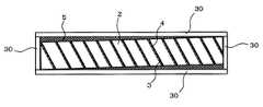
例えば、図4に示すように、上下面および左右面が平行に保たれた金型30を用意し、金型30内に導光板2を入れて、接着剤5または樹脂剤を充填するようにしてもよい。そして、接着剤5または樹脂剤が硬化したところで、図5に示すように金型30を取り外せば、接着剤5または樹脂剤と一体となった導光板2を得ることができる。この場合には、接着剤5または樹脂剤の上面と下面の平坦性と平行度が保たれることになる。なお、平坦性については、導光板2を作成する際に使用する平板部材と同程度の平坦性があればよい。 For example, as shown in FIG. 4, a
<第4実施形態>
本発明の第4実施形態について図6を参照して説明する。図6(A)に示すように、積層構造の導光板2においては、光の出射方向Aに平行な方向において、一の半透過反射層3の端部と、当該一の半透過反射層3に隣接する他の半透過反射層3の端部との間隔dが存在する場合、当該間隔dの領域からは反射光が出射されず、表示される画像に黒スジが現れることがある。<Fourth embodiment>
A fourth embodiment of the present invention will be described with reference to FIG. As shown in FIG. 6A, in the
そこで、本実施形態においては、一の半透過反射層3の端部と、当該一の半透過反射層3に隣接する他の半透過反射層3の端部との間隔dがなくなるように、図6(B)に示すように、積層する光透過性の樹脂材料の厚さが同じ場合には、光の出射方向Aにおける導光板2の厚さwを厚くするようにしてもよい。 Therefore, in the present embodiment, the distance d between the end of one
また、図6(C)に示すように、積層する光透過性の樹脂材料の厚さgを薄くして、一の半透過反射層3の端部と、当該一の半透過反射層3に隣接する他の半透過反射層3の端部との間隔dがなくなるようにしてもよい。 Further, as shown in FIG. 6C, the thickness g of the light-transmitting resin material to be laminated is reduced, and the end of one semi-transmissive
図6(B)および図6(C)のように、一の半透過反射層3の端部と、当該一の半透過反射層3に隣接する他の半透過反射層3の端部との間隔dがなくなるように構成した導光板2を用いて、第1実施形態ないし第3実施形態のように光学デバイス1を構成することにより、黒スジのない良好な画像を表示することができる。 As shown in FIGS. 6B and 6C, the end of one
なお、一の半透過反射層3の端部と、当該一の半透過反射層3に隣接する他の半透過反射層3の端部とが、光の出射方向Aに平行な方向において重なり過ぎると、明スジができる場合があるため、一の半透過反射層3の端部と、当該一の半透過反射層3に隣接する他の半透過反射層3の端部との間隔dがなくなるように、かつ、明スジができない程度に構成することが好ましい。 Note that an end portion of one
<変形例>
本発明は、上述した各実施形態に限定されるものではなく、例えば、以下に述べる各種の変形が可能である。また、各実施形態及び各変形例を適宜組み合わせてもよいことは勿論である。<Modification>
The present invention is not limited to the above-described embodiments, and for example, various modifications described below are possible. Of course, each embodiment and each modification may be combined as appropriate.
(1)半透過反射層の斜向角あるいはピッチについては、上述した黒スジが現れない構成であれば、適宜変更可能である。(1) The oblique angle or pitch of the transflective layer can be appropriately changed as long as the above-described black streaks do not appear.
(2)半透過反射層の反射率は、導光板における光導入部からの光路長の増大に応じて高くなるようにしてもよい。この場合、反射率は、光路長の増大に応じて連続的に変化させてもよいし、段階的に変化させてもよい。このようにすれば、光導入部から離れ、光路長が長くなった場合でも、輝度むらの発生を回避することができる。(2) The reflectivity of the transflective layer may be increased in accordance with an increase in the optical path length from the light introducing portion in the light guide plate. In this case, the reflectance may be continuously changed according to the increase of the optical path length, or may be changed stepwise. In this way, even when the distance from the light introducing portion is increased and the optical path length becomes long, the occurrence of uneven brightness can be avoided.
(3)光学素子の構成については、各実施形態で説明した構成に限定されるものではなく、接着剤を用いて上面平板および下面平板に接着した導光板、あるいは、型抜き等により接着剤でコーティングした導光板であれば、どのような構成の光学デバイスであってもよい。(3) The configuration of the optical element is not limited to the configuration described in each embodiment. The light guide plate is bonded to the upper and lower flat plates using an adhesive, or the adhesive is formed by die cutting or the like. Any optical device with any configuration may be used as long as it is a coated light guide plate.
<応用例>
本発明の光学素子は、例えば、導光板を備えた画像表示装置の1つであるヘッドマウントディスプレイ(HMD)に用いることができる。このようなヘッドマウントディスプレイについて図7を参照して説明する。<Application example>
The optical element of the present invention can be used, for example, in a head mounted display (HMD) that is one of image display devices including a light guide plate. Such a head mounted display will be described with reference to FIG.
図7は、応用例に係るヘッドマウントディスプレイ100の全体像の一例を示す斜視図である。図7に示すように、本実施形態に係るヘッドマウントディスプレイ100は、眼鏡のような外観を有するヘッドマウントディスプレイであり、このヘッドマウントディスプレイ100を装着した観察者に対して虚像による画像光を認識させることができるとともに、観察者に外界像をシースルーで観察させることができる。 FIG. 7 is a perspective view showing an example of the overall image of the head mounted
具体的にヘッドマウントディスプレイ100は、導光板40と、導光板40を支持する左右一対のテンプル131,132と、テンプル131,132に付加された一対の画像形成装置111,112とを備える。ここで、図面上において、導光板40の左側と画像形成装置111とを組み合わせた第1表示装置100Aは、右眼用の虚像を形成する部分であり、単独でも画像表示装置として機能する。また、図面上において、導光板20で右側と画像形成装置112とを組み合わせた第2表示装置100Bは、左眼用の虚像を形成する部分であり、単独でも画像表示装置として機能する。 Specifically, the head mounted
このようなヘッドマウントディスプレイ100において、左眼用光学系の導光板として、図1に示す光学素子を用い、右眼用光学系の導光板として、図1に示す光学デバイスの左右を反転させたものを用いることができる。 In such a head-mounted
1…光学デバイス、2…導光板、3…半透過反射層、4…接着剤、5…接着剤、6…上面平板、7…下面平板、8…導入ブロック、9…投射光取り入れミラー、10…ミラー支持板、11…遮光層、20…画像表示源、30…金型、100…ヘッドマウントディスプレイ、100A,100B…表示装置、111,112…画像形成装置、131,132…テンプル。 DESCRIPTION OF
Claims (12)
Translated fromJapanese前記導光板の第1面に接するように配置された第1透光材と、
前記導光板の前記第1面と反対側に位置する第2面に接するように配置された第2透光材と、を有し、
前記導光板は、透光性の材料からなる第1部分と、透光性の材料からなる第2部分と、前記第1部分と前記第2部分との間に配置された第1半透過反射層と、を備え、
前記第1半透過反射層は、前記第1面及び前記第2面に対して傾斜するように配置され、
前記第1透光材、前記第2透光材、前記第1部分及び前記第2部分は、屈折率が等しく、
前記第1透光材の前記第1面に接する面とは反対側に位置する面は、前記第2透光材の前記第2面に接する面とは反対側に位置する面と、平行となるように配置され、
前記導光板の前記第1面は、前記第1透光材の前記第1面に接する面とは反対側に位置する面に対して傾斜するように配置され、
前記導光板の前記第2面は、前記第2透光材の前記第2面に接する面とは反対側に位置する面に対して傾斜するように配置されていることを特徴とする光学素子。A light guide plate;
A first light transmissive material disposed so as to be in contact with the first surface of the light guide plate;
A second translucent material disposed so as to contact a second surface located on the opposite side of the first surface of the light guide plate,
The light guide plate includes a first part made of a light transmissive material, a second part made of a light transmissive material, and a first transflective reflection disposed between the first part and the second part. A layer, and
The first transflective layer is disposed to be inclined with respect to the first surface and the second surface;
The first light transmissive material, the second light transmissive material, the first portion and the second portion have the same refractive index,
The surface of the first light transmissive material that is located on the opposite side of the surface that contacts the first surface is parallel to the surface of the second light transmissive material that is located on the opposite side of the surface that is in contact with the second surface. Arranged to be
The first surface of the light guide plate is disposed so as to be inclined with respect to a surface located on the side opposite to the surface in contact with the first surface of the first light transmissive material,
The optical element, wherein the second surface of the light guide plate is disposed so as to be inclined with respect to a surface located on a side opposite to a surface in contact with the second surface of thesecond light transmissive material. .
前記導光板の第1面側に配置され、透光性の材料からなる第1基板と、
前記導光板の前記第1面と反対側に位置する第2面側に配置され、透光性の材料からなる第2基板と、
前記導光板と前記第1基板との間に配置された第1透光材と、
前記導光板と前記第2基板との間に配置された第2透光材と、を有し、
前記導光板は、透光性の材料からなる第1部分と、透光性の材料からなる第2部分と、前記第1部分と前記第2部分との間に配置された第1半透過反射層と、を備え、
前記第1半透過反射層は、前記第1面及び前記第2面に対して傾斜するように配置され、
前記第1透光材、前記第2透光材、前記第1部分及び前記第2部分は、屈折率が等しく、
前記第1基板及び前記第2基板は、前記第1透光材及び前記第2透光材とは異なる屈折率であり、
前記第1基板の前記導光板側に位置する面は、前記第2基板の前記導光板側に位置する面と、平行となるように配置され、
前記第1透光材の前記第1面に接する面とは反対側に位置する面は、前記第2透光材の前記第2面に接する面とは反対側に位置する面と、平行となるように配置され、
前記第1基板の前記導光板側に位置する面とは反対側に位置する面は、前記第2基板の前記導光板側に位置する面とは反対側に位置する面と、平行となるように配置され、
前記導光板の前記第1面は、前記第1基板の前記導光板側に位置する面に対して傾斜するように配置され、
前記導光板の前記第2面は、前記第2基板の前記導光板側に位置する面に対して傾斜するように配置されていることを特徴とする光学素子。A light guide plate;
A first substrate disposed on the first surface side of the light guide plate and made of a translucent material;
A second substrate that is disposed on the second surface side opposite to the first surface of the light guide plate and is made of a translucent material;
A first light transmissive material disposed between the light guide plate and the first substrate;
A second light transmissive material disposed between the light guide plate and the second substrate,
The light guide plate includes a first part made of a light transmissive material, a second part made of a light transmissive material, and a first transflective reflection disposed between the first part and the second part. A layer, and
The first transflective layer is disposed to be inclined with respect to the first surface and the second surface;
The first light transmissive material, the second light transmissive material, the first portion and the second portion have the same refractive index,
The first substrate and the second substrate have a refractive index different from that of the first light transmissive material and the second light transmissive material,
The surface located on the light guide plate side of the first substrate is arranged to be parallel to the surface located on the light guide plate side of the second substrate,
The surface of the first light transmissive material that is located on the opposite side of the surface that contacts the first surface is parallel to the surface of the second light transmissive material that is located on the opposite side of the surface that is in contact with the second surface. Arranged to be
The surface of the first substrate located on the opposite side of the surface located on the light guide plate side is parallel to the surface of the second substrate located on the opposite side of the surface located on the light guide plate side. Placed in
The first surface of the light guide plate is disposed to be inclined with respect to a surface located on the light guide plate side of the first substrate,
The optical element, wherein the second surface of the light guide plate is disposed to be inclined with respect to a surface of the second substrate located on the light guide plate side.
前記導光板は、透光性の材料からなる第3部分と、前記第2部分と前記第3部分との間に配置された第2半透過反射層と、を備え、
前記第2半透過反射層は、前記第1半透過反射層と平行になるように配置され、
前記第2半透過反射層は、前記第3部分側から入射した光の少なくとも一部を前記第1面側に向けて反射し、かつ、前記第3部分側から入射した光の他の一部を透過し、
前記第1半透過反射層は、前記第2部分側から入射した前記第2半透過反射層を透過した光の少なくとも一部を前記第1面側に向けて反射することを特徴とする光学素子。The optical element according to claim 1 or 2,
The light guide plate includes a third portion made of a light-transmitting material, and a second transflective layer disposed between the second portion and the third portion,
The second transflective layer is disposed to be parallel to the first transflective layer,
The second transflective layer reflects at least part of the light incident from the third part side toward the first surface side and the other part of the light incident from the third part side. Through
The first semi-transmissive reflective layer reflects at least a part of light transmitted from the second semi-transmissive reflective layer incident from the second portion side toward the first surface side. .
前記第1半透過反射層の前記第2部分側の反射率は、前記第2半透過反射層の前記第3部分側の反射率よりも高いことを特徴とする光学素子。The optical element according to claim 3.
The optical element according to claim 1, wherein a reflectance of the first semi-transmissive reflective layer on the second portion side is higher than a reflectance of the second semi-transmissive reflective layer on the third portion side.
前記第1半透過反射層における、前記第2面側の端部から前記第1面に下ろした垂線は、前記第2半透過反射層の前記第1面側の端部と、前記第1面で交差することを特徴とする光学素子。The optical element according to claim 3 or 4,
In the first transflective layer, a perpendicular line extending from the end on the second surface side to the first surface corresponds to an end on the first surface side of the second transflective layer and the first surface. An optical element characterized by intersecting with each other.
前記第1部分の前記第1半透過反射層と反対側の位置に第1遮光層を有することを特徴とする光学素子。The optical element according to any one of claims 1 to 5,
An optical element comprising a first light shielding layer at a position opposite to the first transflective layer of the first portion.
前記第2透光材の前記導光板と反対側の位置に第2遮光層を有することを特徴とする光学素子。The optical element according to any one of claims 1 to 6,
An optical element comprising a second light shielding layer at a position opposite to the light guide plate of the second light transmissive material.
前記導光板に光を導入する透光性の導入ブロックと、
前記導入ブロックに向かうように光を反射させるミラーと、を有することを特徴とする光学素子。The optical element according to any one of claims 1 to 7,
A translucent introduction block for introducing light into the light guide plate;
An optical element comprising: a mirror that reflects light toward the introduction block.
前記矩形凹部と前記導光板との間隙に、硬化性の透光材を充填する工程と、
前記第1面と前記第2面が前記対向面と傾斜した状態で前記硬化性の透光材を硬化させる工程と、を有し、
前記導光板は、透光性の材料からなる第1部分と、透光性の材料からなる第2部分と、前記第1部分と前記第2部分との間に配置された第1半透過反射層と、を備え、
前記第1半透過反射層は、前記第1面及び前記第2面に対して傾斜するように配置され、
前記硬化性の透光材、前記第1部分及び前記第2部分は、屈折率が等しいことを特徴とする光学素子の製造方法。Placing a light guide plate having a first surface and a second surface located on the opposite side of the first surface in the rectangular recess of the mold having a rectangular recess whose opposing surface is parallel;
Filling a gap between the rectangular recess and the light guide plate with a curable translucent material;
Curing the curable light-transmitting material in a state where the first surface and the second surface are inclined with respect to the facing surface,
The light guide plate includes a first part made of a light transmissive material, a second part made of a light transmissive material, and a first transflective reflection disposed between the first part and the second part. A layer, and
The first transflective layer is disposed to be inclined with respect to the first surface and the second surface;
The method of manufacturing an optical element, wherein the curable light-transmitting material, the first portion, and the second portion have the same refractive index.
前記硬化性の透光材が塗布された前記導光板を、透光性の材料からなる第1基板と透光性の材料からなる第2基板とで挟持する工程と、
前記第1基板の前記導光板側に位置する面とは反対側に位置する面と前記第2基板の前記導光板側に位置する面とは反対側に位置する面とが平行であり、前記第1基板の前記導光板側に位置する面と前記第2基板の前記導光板側に位置する面とが平行で、前記第1基板の前記導光板側に位置する面及び前記第2基板の前記導光板側に位置する面と、前記第1面及び前記第2面とが傾斜した状態で前記硬化性の透光材を硬化させる工程と、を有し、
前記導光板は、透光性の材料からなる第1部分と、透光性の材料からなる第2部分と、前記第1部分と前記第2部分との間に配置された第1半透過反射層と、を備え、
前記第1半透過反射層は、前記第1面及び前記第2面に対して傾斜するように配置され、
前記硬化性の透光材、前記第1部分及び前記第2部分は、屈折率が等しいことを特徴とする光学素子の製造方法。Applying a curable translucent material to a light guide plate having a first surface and a second surface located on the opposite side of the first surface;
Sandwiching the light guide plate coated with the curable translucent material between a first substrate made of a translucent material and a second substrate made of a translucent material;
The surface located on the opposite side of the surface located on the light guide plate side of the first substrate and the surface located on the opposite side of the surface located on the light guide plate side of the second substrate are parallel, The surface of the first substrate located on the light guide plate side and the surface of the second substrate located on the light guide plate side are parallel, and the surface of the first substrate located on the light guide plate side and the second substrate Curing the curable light-transmitting material in a state where the surface located on the light guide plate side and the first surface and the second surface are inclined,
The light guide plate includes a first part made of a light transmissive material, a second part made of a light transmissive material, and a first transflective reflection disposed between the first part and the second part. A layer, and
The first transflective layer is disposed to be inclined with respect to the first surface and the second surface;
The method of manufacturing an optical element, wherein the curable light-transmitting material, the first portion, and the second portion have the same refractive index.
前記導光板は、
前記第1部分となる第1平板部材の一方の面に前記第1半透過反射層を蒸着し、
前記第1平板部材の前記一方の面側に、前記第2部分となる第2平板部材を前記第1半透過反射層の傾向角に応じて、前記第1平板部材と前記第2平板部材とをずらして積層し、
前記積層した前記第1平板部材と前記第2平板部材とを切断することにより形成する、
ことを特徴とする光学素子の製造方法。In the manufacturing method of the optical element according to claim 9 or 10,
The light guide plate is
Depositing the first transflective layer on one surface of the first flat plate member serving as the first portion;
The first flat plate member, the second flat plate member, and the second flat plate member serving as the second portion on the one surface side of the first flat plate member according to the tendency angle of the first transflective layer. Laminating and laminating
Forming the laminated first flat plate member and the second flat plate member by cutting;
A method for manufacturing an optical element.
Priority Applications (6)
| Application Number | Priority Date | Filing Date | Title |
|---|---|---|---|
| JP2013236596AJP6225657B2 (en) | 2013-11-15 | 2013-11-15 | OPTICAL ELEMENT, IMAGE DISPLAY DEVICE, AND MANUFACTURING METHOD THEREOF |
| US14/525,865US9738041B2 (en) | 2013-11-15 | 2014-10-28 | Optical element, image display device and method for manufacturing same |
| KR1020140148181AKR20150056457A (en) | 2013-11-15 | 2014-10-29 | Optical element, image display device and method for manufacturing same |
| TW103139284ATW201518795A (en) | 2013-11-15 | 2014-11-12 | Optical element, image display device and method for manufacturing same |
| CN201410646167.5ACN104656181B (en) | 2013-11-15 | 2014-11-14 | Optical element, image display device and method of manufacturing the same |
| US15/633,180US20170293149A1 (en) | 2013-11-15 | 2017-06-26 | Optical element, image display device and method for manufacturing same |
Applications Claiming Priority (1)
| Application Number | Priority Date | Filing Date | Title |
|---|---|---|---|
| JP2013236596AJP6225657B2 (en) | 2013-11-15 | 2013-11-15 | OPTICAL ELEMENT, IMAGE DISPLAY DEVICE, AND MANUFACTURING METHOD THEREOF |
Publications (2)
| Publication Number | Publication Date |
|---|---|
| JP2015096883A JP2015096883A (en) | 2015-05-21 |
| JP6225657B2true JP6225657B2 (en) | 2017-11-08 |
Family
ID=53173041
Family Applications (1)
| Application Number | Title | Priority Date | Filing Date |
|---|---|---|---|
| JP2013236596AActiveJP6225657B2 (en) | 2013-11-15 | 2013-11-15 | OPTICAL ELEMENT, IMAGE DISPLAY DEVICE, AND MANUFACTURING METHOD THEREOF |
Country Status (5)
| Country | Link |
|---|---|
| US (2) | US9738041B2 (en) |
| JP (1) | JP6225657B2 (en) |
| KR (1) | KR20150056457A (en) |
| CN (1) | CN104656181B (en) |
| TW (1) | TW201518795A (en) |
Families Citing this family (61)
| Publication number | Priority date | Publication date | Assignee | Title |
|---|---|---|---|---|
| US10073264B2 (en) | 2007-08-03 | 2018-09-11 | Lumus Ltd. | Substrate-guide optical device |
| US10261321B2 (en) | 2005-11-08 | 2019-04-16 | Lumus Ltd. | Polarizing optical system |
| JP2015184561A (en)* | 2014-03-25 | 2015-10-22 | ソニー株式会社 | Light guide device, image display device, and display device |
| JP2015184560A (en) | 2014-03-25 | 2015-10-22 | ソニー株式会社 | Light guide device, image display device, and display device |
| IL232197B (en) | 2014-04-23 | 2018-04-30 | Lumus Ltd | Compact head-mounted display system |
| IL235642B (en) | 2014-11-11 | 2021-08-31 | Lumus Ltd | Compact head-mounted display system protected by a hyperfine structure |
| US9759923B2 (en)* | 2015-11-19 | 2017-09-12 | Microsoft Technology Licensing, Llc | Low-stress waveguide mounting for head-mounted display device |
| EP3190447B1 (en)* | 2016-01-06 | 2020-02-05 | Ricoh Company, Ltd. | Light guide and virtual image display device |
| US11262564B2 (en) | 2016-01-18 | 2022-03-01 | Shimadzu Corporation | Optical element, display device using same, and photoreceptor device |
| CN105652448A (en)* | 2016-01-28 | 2016-06-08 | 上海理湃光晶技术有限公司 | Planar waveguide imaging device and method |
| CN105652447B (en)* | 2016-01-28 | 2018-04-03 | 上海理湃光晶技术有限公司 | Slab guide imaging device and method |
| JP6733255B2 (en)* | 2016-03-28 | 2020-07-29 | セイコーエプソン株式会社 | Optical element, display device, and method for manufacturing optical element |
| US10215986B2 (en)* | 2016-05-16 | 2019-02-26 | Microsoft Technology Licensing, Llc | Wedges for light transformation |
| WO2018065975A1 (en) | 2016-10-09 | 2018-04-12 | Lumus Ltd | Aperture multiplier using a rectangular waveguide |
| JP6508160B2 (en)* | 2016-10-17 | 2019-05-08 | トヨタ自動車株式会社 | Vehicle lamp |
| KR20240160657A (en) | 2016-11-08 | 2024-11-11 | 루머스 리미티드 | Light-guide device with optical cutoff edge and corresponding production methods |
| KR102170123B1 (en) | 2016-12-14 | 2020-10-26 | 주식회사 엘지화학 | Waveguide having light shielding and manufacturing method for the same |
| CN106597672B (en)* | 2017-02-16 | 2020-06-16 | 上海鲲游光电科技有限公司 | Augmented reality display device based on waveguide |
| CN108738358B (en) | 2017-02-22 | 2021-03-26 | 鲁姆斯有限公司 | Light guide optics |
| CN109416433B (en)* | 2017-03-22 | 2021-06-01 | 鲁姆斯有限公司 | Overlapping Reflector Construction |
| IL251645B (en)* | 2017-04-06 | 2018-08-30 | Lumus Ltd | Light-guide optical element and method of its manufacture |
| CN117930510A (en) | 2017-04-17 | 2024-04-26 | 阿科尼亚全息有限责任公司 | Imaging assisted by oblique mirror |
| KR102642282B1 (en) | 2017-07-12 | 2024-02-28 | 호야 가부시키가이샤 | Light guide plate and image display device |
| JP2019020723A (en) | 2017-07-12 | 2019-02-07 | Hoya Candeo Optronics株式会社 | Light guide plate and image display device |
| KR102182768B1 (en) | 2017-11-24 | 2020-11-25 | 주식회사 엘지화학 | Waveguide having light shielding and manufacturing method for the same |
| KR102210938B1 (en)* | 2017-11-28 | 2021-02-01 | 주식회사 엘지화학 | A composition for shielding a waveguide edge with excellent adhesion |
| US10551544B2 (en) | 2018-01-21 | 2020-02-04 | Lumus Ltd. | Light-guide optical element with multiple-axis internal aperture expansion |
| CN110161612B (en)* | 2018-02-13 | 2021-03-30 | 华为技术有限公司 | Optical waveguide device, near-eye display apparatus, and terminal |
| MX2020012512A (en) | 2018-05-23 | 2021-02-16 | Lumus Ltd | Optical system including light-guide optical element with partially-reflective internal surfaces. |
| CN112601993A (en) | 2018-08-26 | 2021-04-02 | 鲁姆斯有限公司 | Reflection suppression in near-eye displays |
| CN116184666A (en) | 2018-09-09 | 2023-05-30 | 鲁姆斯有限公司 | Optical system comprising a light-guiding optical element with two-dimensional expansion |
| CN112805622B (en)* | 2018-10-01 | 2022-08-19 | 富士胶片株式会社 | Display device |
| JP2020086346A (en)* | 2018-11-30 | 2020-06-04 | セイコーエプソン株式会社 | Light guide device and virtual image display device |
| EP3671314B1 (en)* | 2018-12-21 | 2024-05-22 | Valeo Vision | Luminous device for vehicle with optical axis adjustment |
| MX2021008808A (en) | 2019-01-24 | 2021-08-24 | Lumus Ltd | Optical systems including loe with three stage expansion. |
| JP7330280B2 (en)* | 2019-02-22 | 2023-08-21 | ビュージックス コーポレーション | Parallel plate waveguide |
| WO2020174433A1 (en) | 2019-02-28 | 2020-09-03 | Lumus Ltd. | Compact collimated image projector |
| EP3956604A4 (en) | 2019-04-15 | 2022-06-08 | Lumus Ltd. | PROCESS FOR MANUFACTURING AN OPTICAL LIGHT GUIDE ELEMENT |
| TWI845670B (en) | 2019-05-06 | 2024-06-21 | 以色列商魯姆斯有限公司 | Transparent lightguide for viewing a scene and a near-eye display |
| CA3137994A1 (en) | 2019-06-27 | 2020-12-30 | Lumus Ltd | Apparatus and methods for eye tracking based on eye imaging via a light-guide optical element |
| AU2020300121B2 (en) | 2019-07-04 | 2024-06-13 | Lumus Ltd. | Image waveguide with symmetric beam multiplication |
| KR20220035088A (en)* | 2019-07-18 | 2022-03-21 | 루머스 리미티드 | Encapsulated light guide optics |
| TWI884834B (en) | 2019-12-05 | 2025-05-21 | 以色列商魯姆斯有限公司 | Optical device and method of fabricating optical device |
| US11523092B2 (en) | 2019-12-08 | 2022-12-06 | Lumus Ltd. | Optical systems with compact image projector |
| IL294151A (en) | 2019-12-30 | 2022-08-01 | Lumus Ltd | Optical systems including light-guiding optical elements with two-dimensional expansion |
| TWI740355B (en)* | 2020-01-20 | 2021-09-21 | 尚立光電股份有限公司 | Light-guide optical element |
| CN119596440A (en)* | 2020-03-13 | 2025-03-11 | 三菱化学株式会社 | Light guide plate and AR display |
| WO2021220267A1 (en) | 2020-04-30 | 2021-11-04 | Lumus Ltd. | Optical sample characterization |
| CN115176190B (en) | 2020-05-24 | 2024-07-09 | 鲁姆斯有限公司 | Composite light guide optical element |
| AU2021279462B2 (en) | 2020-05-24 | 2023-06-08 | Lumus Ltd. | Method of fabrication of compound light-guide optical elements |
| AU2021331833A1 (en)* | 2020-08-23 | 2023-03-09 | Lumus Ltd. | Optical system for two-dimensional expansion of an image reducing glints and ghosts from the waveguide |
| WO2022044006A1 (en) | 2020-08-26 | 2022-03-03 | Lumus Ltd. | Generation of color images using white light as source |
| DE202021104723U1 (en) | 2020-09-11 | 2021-10-18 | Lumus Ltd. | Image projector coupled to an optical light guide element |
| CN116097151B (en) | 2020-11-09 | 2024-04-09 | 鲁姆斯有限公司 | Color Corrected Back Reflection in AR Systems |
| KR20240006707A (en) | 2021-02-25 | 2024-01-15 | 루머스 리미티드 | Optical aperture multipliers having a rectangular waveguide |
| KR20230148324A (en) | 2021-03-01 | 2023-10-24 | 루머스 리미티드 | Optical system with compact coupling from projector to waveguide |
| TW202300988A (en) | 2021-05-19 | 2023-01-01 | 以色列商魯姆斯有限公司 | Active optical engine |
| KR102676604B1 (en) | 2021-07-04 | 2024-06-18 | 루머스 리미티드 | Display with stacked light guiding elements providing different parts of the field of view |
| KR20240046489A (en) | 2021-08-23 | 2024-04-09 | 루머스 리미티드 | Method for manufacturing composite light guiding optical elements with embedded coupling-in reflector |
| WO2024038458A1 (en) | 2022-08-18 | 2024-02-22 | Lumus Ltd. | Image projector with polarizing catadioptric collimator |
| TWI855873B (en)* | 2023-09-22 | 2024-09-11 | 澤米科技股份有限公司 | Light-guide optical element and its manufacturing method |
Family Cites Families (22)
| Publication number | Priority date | Publication date | Assignee | Title |
|---|---|---|---|---|
| JPS63228188A (en)* | 1987-03-17 | 1988-09-22 | ソニー株式会社 | Liquid crystal display device |
| JPH06337316A (en) | 1993-05-28 | 1994-12-06 | Nissan Motor Co Ltd | Display device |
| KR100234896B1 (en)* | 1997-07-29 | 1999-12-15 | 구본준 | Substrate flattening method of liquid crystal display |
| ATE473464T1 (en)* | 2000-06-05 | 2010-07-15 | Lumus Ltd | OPTICAL BEAM EXPANDER WITH SUBSTRATE LIGHT WAVE GUIDE |
| US6563648B2 (en)* | 2000-10-20 | 2003-05-13 | Three-Five Systems, Inc. | Compact wide field of view imaging system |
| US6861015B2 (en)* | 2001-07-20 | 2005-03-01 | Au Optronics Corporation | Method of integrally forming light-guide and polarizer |
| EP1748305A4 (en) | 2004-05-17 | 2009-01-14 | Nikon Corp | Optical element, combiner optical system, and image display unit |
| JP4742575B2 (en) | 2004-12-03 | 2011-08-10 | 株式会社ニコン | Image display optical system and image display apparatus |
| KR20080064902A (en)* | 2004-08-25 | 2008-07-09 | 문더기 테트놀로지스, 인크. | Wireless Digitizer Tablet and Digitizer Tablet Computer |
| TW200712653A (en)* | 2005-09-28 | 2007-04-01 | Jemitek Electronics Corp | Liquid crystal having function of micro-reflection |
| IL171820A (en)* | 2005-11-08 | 2014-04-30 | Lumus Ltd | Polarizing optical device for light coupling |
| JP2007219106A (en)* | 2006-02-16 | 2007-08-30 | Konica Minolta Holdings Inc | Optical device for expanding diameter of luminous flux, video display device and head mount display |
| US7826113B2 (en)* | 2007-03-28 | 2010-11-02 | Konica Minolta Holdings, Inc. | Joined optical member, image display apparatus, and head-mounted display |
| JP2009145513A (en) | 2007-12-13 | 2009-07-02 | Konica Minolta Holdings Inc | Video display apparatus and head mount display |
| JP5146368B2 (en)* | 2009-03-10 | 2013-02-20 | セイコーエプソン株式会社 | Method for manufacturing optical article |
| JP5608385B2 (en)* | 2010-02-08 | 2014-10-15 | デクセリアルズ株式会社 | OPTICAL BODY, MANUFACTURING METHOD THEREFOR, WINDOW MATERIAL, JOINT, AND sunshine blocking device |
| JP5471986B2 (en)* | 2010-09-07 | 2014-04-16 | 株式会社島津製作所 | Optical component and display device using the same |
| JP5732808B2 (en) | 2010-10-19 | 2015-06-10 | セイコーエプソン株式会社 | Virtual image display device |
| KR101894898B1 (en)* | 2011-02-11 | 2018-09-04 | 가부시키가이샤 한도오따이 에네루기 켄큐쇼 | Light-emitting device and electronic device using light-emitting device |
| JP2012252091A (en)* | 2011-06-01 | 2012-12-20 | Sony Corp | Display apparatus |
| JP2013130693A (en)* | 2011-12-21 | 2013-07-04 | Teijin Chem Ltd | Light guide plate |
| TW201337349A (en)* | 2012-03-12 | 2013-09-16 | Innocom Tech Shenzhen Co Ltd | Optical element and display system |
- 2013
- 2013-11-15JPJP2013236596Apatent/JP6225657B2/enactiveActive
- 2014
- 2014-10-28USUS14/525,865patent/US9738041B2/enactiveActive
- 2014-10-29KRKR1020140148181Apatent/KR20150056457A/ennot_activeWithdrawn
- 2014-11-12TWTW103139284Apatent/TW201518795A/enunknown
- 2014-11-14CNCN201410646167.5Apatent/CN104656181B/enactiveActive
- 2017
- 2017-06-26USUS15/633,180patent/US20170293149A1/ennot_activeAbandoned
Also Published As
| Publication number | Publication date |
|---|---|
| KR20150056457A (en) | 2015-05-26 |
| JP2015096883A (en) | 2015-05-21 |
| US20150138646A1 (en) | 2015-05-21 |
| TW201518795A (en) | 2015-05-16 |
| CN104656181A (en) | 2015-05-27 |
| US9738041B2 (en) | 2017-08-22 |
| CN104656181B (en) | 2019-06-21 |
| US20170293149A1 (en) | 2017-10-12 |
Similar Documents
| Publication | Publication Date | Title |
|---|---|---|
| JP6225657B2 (en) | OPTICAL ELEMENT, IMAGE DISPLAY DEVICE, AND MANUFACTURING METHOD THEREOF | |
| US10802289B2 (en) | Virtual image display device | |
| US10365489B2 (en) | Semi-transmissive reflection sheet, light guide plate and display device | |
| US11143872B2 (en) | Waveguide and video image display device | |
| CN102628990B (en) | Virtual image display apparatus | |
| CN107193078B (en) | A kind of optical waveguide and its preparation method, augmented reality equipment | |
| JP5817904B1 (en) | Light guide plate, display device | |
| JP2012163658A (en) | Virtual image display device | |
| JP6600952B2 (en) | Transflective reflection sheet, display device | |
| JP6115004B2 (en) | Virtual image display device and method of manufacturing virtual image display device | |
| JP5983790B2 (en) | Transflective reflection sheet, light guide plate, display device | |
| JP2013080039A (en) | Virtual image display device and method for manufacturing the same | |
| JP5843043B1 (en) | Light guide plate, display device | |
| JP6027155B2 (en) | Transflective reflection sheet, display device | |
| JP5896075B1 (en) | Light guide plate, display device | |
| JP2016188962A (en) | Transflective sheet and display device | |
| JP6565458B2 (en) | Optical sheet, display device | |
| JP6147311B2 (en) | Transflective reflection sheet, display device | |
| JP2017003937A (en) | Optical sheet, display device | |
| JP6398712B2 (en) | Light guide plate, display device | |
| JP2016170373A (en) | Transflective sheet and display device | |
| JP2016170374A (en) | Transflective sheet, display device, and manufacturing method for transflective sheet |
Legal Events
| Date | Code | Title | Description |
|---|---|---|---|
| RD04 | Notification of resignation of power of attorney | Free format text:JAPANESE INTERMEDIATE CODE: A7424 Effective date:20160617 | |
| RD03 | Notification of appointment of power of attorney | Free format text:JAPANESE INTERMEDIATE CODE: A7423 Effective date:20160624 | |
| A621 | Written request for application examination | Free format text:JAPANESE INTERMEDIATE CODE: A621 Effective date:20161102 | |
| A977 | Report on retrieval | Free format text:JAPANESE INTERMEDIATE CODE: A971007 Effective date:20170614 | |
| A131 | Notification of reasons for refusal | Free format text:JAPANESE INTERMEDIATE CODE: A131 Effective date:20170620 | |
| RD02 | Notification of acceptance of power of attorney | Free format text:JAPANESE INTERMEDIATE CODE: A7422 Effective date:20170726 | |
| A521 | Written amendment | Free format text:JAPANESE INTERMEDIATE CODE: A523 Effective date:20170808 | |
| A131 | Notification of reasons for refusal | Free format text:JAPANESE INTERMEDIATE CODE: A131 Effective date:20170822 | |
| A521 | Written amendment | Free format text:JAPANESE INTERMEDIATE CODE: A523 Effective date:20170831 | |
| TRDD | Decision of grant or rejection written | ||
| A01 | Written decision to grant a patent or to grant a registration (utility model) | Free format text:JAPANESE INTERMEDIATE CODE: A01 Effective date:20170912 | |
| A61 | First payment of annual fees (during grant procedure) | Free format text:JAPANESE INTERMEDIATE CODE: A61 Effective date:20170925 | |
| R150 | Certificate of patent or registration of utility model | Ref document number:6225657 Country of ref document:JP Free format text:JAPANESE INTERMEDIATE CODE: R150 |