JP6220497B2 - Light emitting device - Google Patents
Light emitting deviceDownload PDFInfo
- Publication number
- JP6220497B2 JP6220497B2JP2012124017AJP2012124017AJP6220497B2JP 6220497 B2JP6220497 B2JP 6220497B2JP 2012124017 AJP2012124017 AJP 2012124017AJP 2012124017 AJP2012124017 AJP 2012124017AJP 6220497 B2JP6220497 B2JP 6220497B2
- Authority
- JP
- Japan
- Prior art keywords
- light
- abbreviation
- electrode
- layer
- substrate
- Prior art date
- Legal status (The legal status is an assumption and is not a legal conclusion. Google has not performed a legal analysis and makes no representation as to the accuracy of the status listed.)
- Expired - Fee Related
Links
- 238000007789sealingMethods0.000claimsdescription52
- 239000003566sealing materialSubstances0.000claimsdescription34
- 239000010410layerSubstances0.000description235
- 239000000758substrateSubstances0.000description127
- 239000000126substanceSubstances0.000description87
- 239000000463materialSubstances0.000description66
- 238000000034methodMethods0.000description53
- 239000011347resinSubstances0.000description44
- 229920005989resinPolymers0.000description44
- -1polyethylene terephthalatePolymers0.000description36
- 238000002347injectionMethods0.000description29
- 239000007924injectionSubstances0.000description29
- 229910052757nitrogenInorganic materials0.000description26
- 238000005192partitionMethods0.000description25
- 239000002131composite materialSubstances0.000description24
- 150000001875compoundsChemical class0.000description20
- 230000005525hole transportEffects0.000description19
- 239000001301oxygenSubstances0.000description18
- 229910052760oxygenInorganic materials0.000description18
- 229910052751metalInorganic materials0.000description17
- 239000002184metalSubstances0.000description17
- CUJRVFIICFDLGR-UHFFFAOYSA-NacetylacetonateChemical compoundCC(=O)[CH-]C(C)=OCUJRVFIICFDLGR-UHFFFAOYSA-N0.000description16
- 150000002894organic compoundsChemical class0.000description16
- 238000000295emission spectrumMethods0.000description14
- 239000002245particleSubstances0.000description14
- 239000000872bufferSubstances0.000description13
- 238000004519manufacturing processMethods0.000description13
- RYGMFSIKBFXOCR-UHFFFAOYSA-NCopperChemical compound[Cu]RYGMFSIKBFXOCR-UHFFFAOYSA-N0.000description12
- PXHVJJICTQNCMI-UHFFFAOYSA-NNickelChemical compound[Ni]PXHVJJICTQNCMI-UHFFFAOYSA-N0.000description12
- 229910045601alloyInorganic materials0.000description12
- 239000000956alloySubstances0.000description12
- 229910052782aluminiumInorganic materials0.000description12
- XAGFODPZIPBFFR-UHFFFAOYSA-NaluminiumChemical compound[Al]XAGFODPZIPBFFR-UHFFFAOYSA-N0.000description12
- 239000010949copperSubstances0.000description12
- QVGXLLKOCUKJST-UHFFFAOYSA-Natomic oxygenChemical compound[O]QVGXLLKOCUKJST-UHFFFAOYSA-N0.000description11
- 229910052799carbonInorganic materials0.000description11
- 238000007650screen-printingMethods0.000description11
- AZFHXIBNMPIGOD-UHFFFAOYSA-N4-hydroxypent-3-en-2-one iridiumChemical compound[Ir].CC(O)=CC(C)=O.CC(O)=CC(C)=O.CC(O)=CC(C)=OAZFHXIBNMPIGOD-UHFFFAOYSA-N0.000description10
- XEEYBQQBJWHFJM-UHFFFAOYSA-NIronChemical compound[Fe]XEEYBQQBJWHFJM-UHFFFAOYSA-N0.000description10
- MILUBEOXRNEUHS-UHFFFAOYSA-Niridium(3+)Chemical compound[Ir+3]MILUBEOXRNEUHS-UHFFFAOYSA-N0.000description10
- 239000000565sealantSubstances0.000description10
- BQCADISMDOOEFD-UHFFFAOYSA-NSilverChemical compound[Ag]BQCADISMDOOEFD-UHFFFAOYSA-N0.000description9
- 239000007983Tris bufferSubstances0.000description9
- 150000004649carbonic acid derivativesChemical class0.000description9
- 150000004820halidesChemical class0.000description9
- 238000004768lowest unoccupied molecular orbitalMethods0.000description9
- IEQIEDJGQAUEQZ-UHFFFAOYSA-NphthalocyanineChemical compoundN1C(N=C2C3=CC=CC=C3C(N=C3C4=CC=CC=C4C(=N4)N3)=N2)=C(C=CC=C2)C2=C1N=C1C2=CC=CC=C2C4=N1IEQIEDJGQAUEQZ-UHFFFAOYSA-N0.000description9
- 229910052709silverInorganic materials0.000description9
- 239000004332silverSubstances0.000description9
- KDLHZDBZIXYQEI-UHFFFAOYSA-NPalladiumChemical compound[Pd]KDLHZDBZIXYQEI-UHFFFAOYSA-N0.000description8
- XLOMVQKBTHCTTD-UHFFFAOYSA-NZinc monoxideChemical compound[Zn]=OXLOMVQKBTHCTTD-UHFFFAOYSA-N0.000description8
- 229910052802copperInorganic materials0.000description8
- 239000007769metal materialSubstances0.000description8
- BASFCYQUMIYNBI-UHFFFAOYSA-NplatinumChemical compound[Pt]BASFCYQUMIYNBI-UHFFFAOYSA-N0.000description8
- 238000004544sputter depositionMethods0.000description8
- RTAQQCXQSZGOHL-UHFFFAOYSA-NTitaniumChemical compound[Ti]RTAQQCXQSZGOHL-UHFFFAOYSA-N0.000description7
- 125000005595acetylacetonate groupChemical group0.000description7
- 150000004696coordination complexChemical class0.000description7
- 238000000059patterningMethods0.000description7
- 125000001997phenyl groupChemical group[H]C1=C([H])C([H])=C(*)C([H])=C1[H]0.000description7
- 229910052719titaniumInorganic materials0.000description7
- 239000010936titaniumSubstances0.000description7
- 229910001316Ag alloyInorganic materials0.000description6
- 229910000838Al alloyInorganic materials0.000description6
- MWPLVEDNUUSJAV-UHFFFAOYSA-NanthraceneChemical compoundC1=CC=CC2=CC3=CC=CC=C3C=C21MWPLVEDNUUSJAV-UHFFFAOYSA-N0.000description6
- 230000001747exhibiting effectEffects0.000description6
- 239000007850fluorescent dyeSubstances0.000description6
- 238000005286illuminationMethods0.000description6
- 239000003446ligandSubstances0.000description6
- 229910052759nickelInorganic materials0.000description6
- 230000008569processEffects0.000description6
- 230000004888barrier functionEffects0.000description5
- 238000000576coating methodMethods0.000description5
- 238000001704evaporationMethods0.000description5
- 238000000605extractionMethods0.000description5
- 239000012535impuritySubstances0.000description5
- 229910052742ironInorganic materials0.000description5
- 229910044991metal oxideInorganic materials0.000description5
- 150000004706metal oxidesChemical class0.000description5
- 238000000206photolithographyMethods0.000description5
- 229920000642polymerPolymers0.000description5
- 229910052761rare earth metalInorganic materials0.000description5
- ZVFQEOPUXVPSLB-UHFFFAOYSA-N3-(4-tert-butylphenyl)-4-phenyl-5-(4-phenylphenyl)-1,2,4-triazoleChemical compoundC1=CC(C(C)(C)C)=CC=C1C(N1C=2C=CC=CC=2)=NN=C1C1=CC=C(C=2C=CC=CC=2)C=C1ZVFQEOPUXVPSLB-UHFFFAOYSA-N0.000description4
- DHDHJYNTEFLIHY-UHFFFAOYSA-N4,7-diphenyl-1,10-phenanthrolineChemical compoundC1=CC=CC=C1C1=CC=NC2=C1C=CC1=C(C=3C=CC=CC=3)C=CN=C21DHDHJYNTEFLIHY-UHFFFAOYSA-N0.000description4
- VYZAMTAEIAYCRO-UHFFFAOYSA-NChromiumChemical compound[Cr]VYZAMTAEIAYCRO-UHFFFAOYSA-N0.000description4
- 229910000881Cu alloyInorganic materials0.000description4
- ZOKXTWBITQBERF-UHFFFAOYSA-NMolybdenumChemical compound[Mo]ZOKXTWBITQBERF-UHFFFAOYSA-N0.000description4
- 229910052783alkali metalInorganic materials0.000description4
- 150000001340alkali metalsChemical class0.000description4
- 150000001491aromatic compoundsChemical class0.000description4
- 239000012298atmosphereSubstances0.000description4
- 230000008859changeEffects0.000description4
- 229910052804chromiumInorganic materials0.000description4
- 239000011651chromiumSubstances0.000description4
- 229910017052cobaltInorganic materials0.000description4
- 239000010941cobaltSubstances0.000description4
- GUTLYIVDDKVIGB-UHFFFAOYSA-Ncobalt atomChemical compound[Co]GUTLYIVDDKVIGB-UHFFFAOYSA-N0.000description4
- 230000000295complement effectEffects0.000description4
- XCJYREBRNVKWGJ-UHFFFAOYSA-Ncopper(II) phthalocyanineChemical compound[Cu+2].C12=CC=CC=C2C(N=C2[N-]C(C3=CC=CC=C32)=N2)=NC1=NC([C]1C=CC=CC1=1)=NC=1N=C1[C]3C=CC=CC3=C2[N-]1XCJYREBRNVKWGJ-UHFFFAOYSA-N0.000description4
- 239000002274desiccantSubstances0.000description4
- ZUOUZKKEUPVFJK-UHFFFAOYSA-NdiphenylChemical compoundC1=CC=CC=C1C1=CC=CC=C1ZUOUZKKEUPVFJK-UHFFFAOYSA-N0.000description4
- 239000007789gasSubstances0.000description4
- PCHJSUWPFVWCPO-UHFFFAOYSA-NgoldChemical compound[Au]PCHJSUWPFVWCPO-UHFFFAOYSA-N0.000description4
- 229910052737goldInorganic materials0.000description4
- 239000010931goldSubstances0.000description4
- FUJCRWPEOMXPAD-UHFFFAOYSA-Nlithium oxideChemical compound[Li+].[Li+].[O-2]FUJCRWPEOMXPAD-UHFFFAOYSA-N0.000description4
- 229910001947lithium oxideInorganic materials0.000description4
- 229910052750molybdenumInorganic materials0.000description4
- 239000011733molybdenumSubstances0.000description4
- 150000004767nitridesChemical class0.000description4
- 229910052763palladiumInorganic materials0.000description4
- 230000002093peripheral effectEffects0.000description4
- 229910052697platinumInorganic materials0.000description4
- 229920003227poly(N-vinyl carbazole)Polymers0.000description4
- 229920001721polyimidePolymers0.000description4
- 238000007639printingMethods0.000description4
- 150000002909rare earth metal compoundsChemical class0.000description4
- 150000002910rare earth metalsChemical class0.000description4
- WFKWXMTUELFFGS-UHFFFAOYSA-NtungstenChemical compound[W]WFKWXMTUELFFGS-UHFFFAOYSA-N0.000description4
- 229910052721tungstenInorganic materials0.000description4
- 239000010937tungstenSubstances0.000description4
- 239000011787zinc oxideSubstances0.000description4
- IYZMXHQDXZKNCY-UHFFFAOYSA-N1-n,1-n-diphenyl-4-n,4-n-bis[4-(n-phenylanilino)phenyl]benzene-1,4-diamineChemical compoundC1=CC=CC=C1N(C=1C=CC(=CC=1)N(C=1C=CC(=CC=1)N(C=1C=CC=CC=1)C=1C=CC=CC=1)C=1C=CC(=CC=1)N(C=1C=CC=CC=1)C=1C=CC=CC=1)C1=CC=CC=C1IYZMXHQDXZKNCY-UHFFFAOYSA-N0.000description3
- 1250000016371-naphthyl groupChemical group[H]C1=C([H])C([H])=C2C(*)=C([H])C([H])=C([H])C2=C1[H]0.000description3
- FQJQNLKWTRGIEB-UHFFFAOYSA-N2-(4-tert-butylphenyl)-5-[3-[5-(4-tert-butylphenyl)-1,3,4-oxadiazol-2-yl]phenyl]-1,3,4-oxadiazoleChemical compoundC1=CC(C(C)(C)C)=CC=C1C1=NN=C(C=2C=C(C=CC=2)C=2OC(=NN=2)C=2C=CC(=CC=2)C(C)(C)C)O1FQJQNLKWTRGIEB-UHFFFAOYSA-N0.000description3
- VFUDMQLBKNMONU-UHFFFAOYSA-N9-[4-(4-carbazol-9-ylphenyl)phenyl]carbazoleChemical groupC12=CC=CC=C2C2=CC=CC=C2N1C1=CC=C(C=2C=CC(=CC=2)N2C3=CC=CC=C3C3=CC=CC=C32)C=C1VFUDMQLBKNMONU-UHFFFAOYSA-N0.000description3
- UHOVQNZJYSORNB-UHFFFAOYSA-NBenzeneChemical compoundC1=CC=CC=C1UHOVQNZJYSORNB-UHFFFAOYSA-N0.000description3
- FYYHWMGAXLPEAU-UHFFFAOYSA-NMagnesiumChemical compound[Mg]FYYHWMGAXLPEAU-UHFFFAOYSA-N0.000description3
- YNPNZTXNASCQKK-UHFFFAOYSA-NPhenanthreneNatural productsC1=CC=C2C3=CC=CC=C3C=CC2=C1YNPNZTXNASCQKK-UHFFFAOYSA-N0.000description3
- GWEVSGVZZGPLCZ-UHFFFAOYSA-NTitan oxideChemical compoundO=[Ti]=OGWEVSGVZZGPLCZ-UHFFFAOYSA-N0.000description3
- DGEZNRSVGBDHLK-UHFFFAOYSA-N[1,10]phenanthrolineChemical compoundC1=CN=C2C3=NC=CC=C3C=CC2=C1DGEZNRSVGBDHLK-UHFFFAOYSA-N0.000description3
- 239000000853adhesiveSubstances0.000description3
- 230000001070adhesive effectEffects0.000description3
- 150000001339alkali metal compoundsChemical class0.000description3
- 229910052784alkaline earth metalInorganic materials0.000description3
- 150000001342alkaline earth metalsChemical class0.000description3
- 150000004945aromatic hydrocarbonsChemical class0.000description3
- 125000003118aryl groupChemical group0.000description3
- 239000002585baseSubstances0.000description3
- GQVWHWAWLPCBHB-UHFFFAOYSA-Lberyllium;benzo[h]quinolin-10-olateChemical compound[Be+2].C1=CC=NC2=C3C([O-])=CC=CC3=CC=C21.C1=CC=NC2=C3C([O-])=CC=CC3=CC=C21GQVWHWAWLPCBHB-UHFFFAOYSA-L0.000description3
- 230000005540biological transmissionEffects0.000description3
- 239000004305biphenylSubstances0.000description3
- FJDQFPXHSGXQBY-UHFFFAOYSA-Lcaesium carbonateChemical compound[Cs+].[Cs+].[O-]C([O-])=OFJDQFPXHSGXQBY-UHFFFAOYSA-L0.000description3
- 229910000024caesium carbonateInorganic materials0.000description3
- 150000001716carbazolesChemical class0.000description3
- 239000003086colorantSubstances0.000description3
- 238000002425crystallisationMethods0.000description3
- 230000008025crystallizationEffects0.000description3
- 238000010586diagramMethods0.000description3
- 230000000694effectsEffects0.000description3
- 238000005530etchingMethods0.000description3
- 239000011521glassSubstances0.000description3
- XGZVUEUWXADBQD-UHFFFAOYSA-Llithium carbonateChemical compound[Li+].[Li+].[O-]C([O-])=OXGZVUEUWXADBQD-UHFFFAOYSA-L0.000description3
- 229910052808lithium carbonateInorganic materials0.000description3
- 239000011777magnesiumSubstances0.000description3
- AMWRITDGCCNYAT-UHFFFAOYSA-Lmanganese oxideInorganic materials[Mn].O[Mn]=O.O[Mn]=OAMWRITDGCCNYAT-UHFFFAOYSA-L0.000description3
- 229910000476molybdenum oxideInorganic materials0.000description3
- QJGQUHMNIGDVPM-UHFFFAOYSA-Nnitrogen groupChemical group[N]QJGQUHMNIGDVPM-UHFFFAOYSA-N0.000description3
- 125000002524organometallic groupChemical group0.000description3
- 230000003647oxidationEffects0.000description3
- 238000007254oxidation reactionMethods0.000description3
- PQQKPALAQIIWST-UHFFFAOYSA-NoxomolybdenumChemical compound[Mo]=OPQQKPALAQIIWST-UHFFFAOYSA-N0.000description3
- 125000002080perylenyl groupChemical groupC1(=CC=C2C=CC=C3C4=CC=CC5=CC=CC(C1=C23)=C45)*0.000description3
- 125000000951phenoxy groupChemical group[H]C1=C([H])C([H])=C(O*)C([H])=C1[H]0.000description3
- 229920003023plasticPolymers0.000description3
- 239000004033plasticSubstances0.000description3
- 229920006122polyamide resinPolymers0.000description3
- 239000009719polyimide resinSubstances0.000description3
- YYMBJDOZVAITBP-UHFFFAOYSA-NrubreneChemical compoundC1=CC=CC=C1C(C1=C(C=2C=CC=CC=2)C2=CC=CC=C2C(C=2C=CC=CC=2)=C11)=C(C=CC=C2)C2=C1C1=CC=CC=C1YYMBJDOZVAITBP-UHFFFAOYSA-N0.000description3
- OGIDPMRJRNCKJF-UHFFFAOYSA-Ntitanium oxideInorganic materials[Ti]=OOGIDPMRJRNCKJF-UHFFFAOYSA-N0.000description3
- ODHXBMXNKOYIBV-UHFFFAOYSA-NtriphenylamineChemical compoundC1=CC=CC=C1N(C=1C=CC=CC=1)C1=CC=CC=C1ODHXBMXNKOYIBV-UHFFFAOYSA-N0.000description3
- 238000007740vapor depositionMethods0.000description3
- UHXOHPVVEHBKKT-UHFFFAOYSA-N1-(2,2-diphenylethenyl)-4-[4-(2,2-diphenylethenyl)phenyl]benzeneChemical groupC=1C=C(C=2C=CC(C=C(C=3C=CC=CC=3)C=3C=CC=CC=3)=CC=2)C=CC=1C=C(C=1C=CC=CC=1)C1=CC=CC=C1UHXOHPVVEHBKKT-UHFFFAOYSA-N0.000description2
- HDMYKJVSQIHZLM-UHFFFAOYSA-N1-[3,5-di(pyren-1-yl)phenyl]pyreneChemical compoundC1=CC(C=2C=C(C=C(C=2)C=2C3=CC=C4C=CC=C5C=CC(C3=C54)=CC=2)C=2C3=CC=C4C=CC=C5C=CC(C3=C54)=CC=2)=C2C=CC3=CC=CC4=CC=C1C2=C43HDMYKJVSQIHZLM-UHFFFAOYSA-N0.000description2
- SPDPTFAJSFKAMT-UHFFFAOYSA-N1-n-[4-[4-(n-[4-(3-methyl-n-(3-methylphenyl)anilino)phenyl]anilino)phenyl]phenyl]-4-n,4-n-bis(3-methylphenyl)-1-n-phenylbenzene-1,4-diamineChemical compoundCC1=CC=CC(N(C=2C=CC(=CC=2)N(C=2C=CC=CC=2)C=2C=CC(=CC=2)C=2C=CC(=CC=2)N(C=2C=CC=CC=2)C=2C=CC(=CC=2)N(C=2C=C(C)C=CC=2)C=2C=C(C)C=CC=2)C=2C=C(C)C=CC=2)=C1SPDPTFAJSFKAMT-UHFFFAOYSA-N0.000description2
- STTGYIUESPWXOW-UHFFFAOYSA-N2,9-dimethyl-4,7-diphenyl-1,10-phenanthrolineChemical compoundC=12C=CC3=C(C=4C=CC=CC=4)C=C(C)N=C3C2=NC(C)=CC=1C1=CC=CC=C1STTGYIUESPWXOW-UHFFFAOYSA-N0.000description2
- UOCMXZLNHQBBOS-UHFFFAOYSA-N2-(1,3-benzoxazol-2-yl)phenol zincChemical compound[Zn].Oc1ccccc1-c1nc2ccccc2o1.Oc1ccccc1-c1nc2ccccc2o1UOCMXZLNHQBBOS-UHFFFAOYSA-N0.000description2
- GEQBRULPNIVQPP-UHFFFAOYSA-N2-[3,5-bis(1-phenylbenzimidazol-2-yl)phenyl]-1-phenylbenzimidazoleChemical compoundC1=CC=CC=C1N1C2=CC=CC=C2N=C1C1=CC(C=2N(C3=CC=CC=C3N=2)C=2C=CC=CC=2)=CC(C=2N(C3=CC=CC=C3N=2)C=2C=CC=CC=2)=C1GEQBRULPNIVQPP-UHFFFAOYSA-N0.000description2
- OBAJPWYDYFEBTF-UHFFFAOYSA-N2-tert-butyl-9,10-dinaphthalen-2-ylanthraceneChemical compoundC1=CC=CC2=CC(C3=C4C=CC=CC4=C(C=4C=C5C=CC=CC5=CC=4)C4=CC=C(C=C43)C(C)(C)C)=CC=C21OBAJPWYDYFEBTF-UHFFFAOYSA-N0.000description2
- 1250000012554-fluorophenyl groupChemical group[H]C1=C([H])C(*)=C([H])C([H])=C1F0.000description2
- USIXUMGAHVBSHQ-UHFFFAOYSA-N9,10-bis(3,5-diphenylphenyl)anthraceneChemical compoundC1=CC=CC=C1C1=CC(C=2C=CC=CC=2)=CC(C=2C3=CC=CC=C3C(C=3C=C(C=C(C=3)C=3C=CC=CC=3)C=3C=CC=CC=3)=C3C=CC=CC3=2)=C1USIXUMGAHVBSHQ-UHFFFAOYSA-N0.000description2
- FCNCGHJSNVOIKE-UHFFFAOYSA-N9,10-diphenylanthraceneChemical compoundC1=CC=CC=C1C(C1=CC=CC=C11)=C(C=CC=C2)C2=C1C1=CC=CC=C1FCNCGHJSNVOIKE-UHFFFAOYSA-N0.000description2
- SXGIRTCIFPJUEQ-UHFFFAOYSA-N9-anthracen-9-ylanthraceneChemical groupC1=CC=CC2=CC3=CC=CC=C3C(C=3C4=CC=CC=C4C=C4C=CC=CC4=3)=C21SXGIRTCIFPJUEQ-UHFFFAOYSA-N0.000description2
- 239000004925Acrylic resinSubstances0.000description2
- 229920000178Acrylic resinPolymers0.000description2
- OKTJSMMVPCPJKN-UHFFFAOYSA-NCarbonChemical compound[C]OKTJSMMVPCPJKN-UHFFFAOYSA-N0.000description2
- GYHNNYVSQQEPJS-UHFFFAOYSA-NGalliumChemical compound[Ga]GYHNNYVSQQEPJS-UHFFFAOYSA-N0.000description2
- 229910000861Mg alloyInorganic materials0.000description2
- 229910052779NeodymiumInorganic materials0.000description2
- 229920001609Poly(3,4-ethylenedioxythiophene)Polymers0.000description2
- NRTOMJZYCJJWKI-UHFFFAOYSA-NTitanium nitrideChemical compound[Ti]#NNRTOMJZYCJJWKI-UHFFFAOYSA-N0.000description2
- WGLPBDUCMAPZCE-UHFFFAOYSA-NTrioxochromiumChemical compoundO=[Cr](=O)=OWGLPBDUCMAPZCE-UHFFFAOYSA-N0.000description2
- XHCLAFWTIXFWPH-UHFFFAOYSA-N[O-2].[O-2].[O-2].[O-2].[O-2].[V+5].[V+5]Chemical compound[O-2].[O-2].[O-2].[O-2].[O-2].[V+5].[V+5]XHCLAFWTIXFWPH-UHFFFAOYSA-N0.000description2
- SORGEQQSQGNZFI-UHFFFAOYSA-N[azido(phenoxy)phosphoryl]oxybenzeneChemical compoundC=1C=CC=CC=1OP(=O)(N=[N+]=[N-])OC1=CC=CC=C1SORGEQQSQGNZFI-UHFFFAOYSA-N0.000description2
- 239000003463adsorbentSubstances0.000description2
- 150000001341alkaline earth metal compoundsChemical class0.000description2
- REDXJYDRNCIFBQ-UHFFFAOYSA-Naluminium(3+)Chemical compound[Al+3]REDXJYDRNCIFBQ-UHFFFAOYSA-N0.000description2
- QVQLCTNNEUAWMS-UHFFFAOYSA-Nbarium oxideChemical compound[Ba]=OQVQLCTNNEUAWMS-UHFFFAOYSA-N0.000description2
- 230000008901benefitEffects0.000description2
- 125000005605benzo groupChemical group0.000description2
- UMIVXZPTRXBADB-UHFFFAOYSA-NbenzocyclobuteneChemical compoundC1=CC=C2CCC2=C1UMIVXZPTRXBADB-UHFFFAOYSA-N0.000description2
- 230000015572biosynthetic processEffects0.000description2
- 235000010290biphenylNutrition0.000description2
- UFVXQDWNSAGPHN-UHFFFAOYSA-Kbis[(2-methylquinolin-8-yl)oxy]-(4-phenylphenoxy)alumaneChemical compound[Al+3].C1=CC=C([O-])C2=NC(C)=CC=C21.C1=CC=C([O-])C2=NC(C)=CC=C21.C1=CC([O-])=CC=C1C1=CC=CC=C1UFVXQDWNSAGPHN-UHFFFAOYSA-K0.000description2
- XZCJVWCMJYNSQO-UHFFFAOYSA-Nbutyl pbdChemical compoundC1=CC(C(C)(C)C)=CC=C1C1=NN=C(C=2C=CC(=CC=2)C=2C=CC=CC=2)O1XZCJVWCMJYNSQO-UHFFFAOYSA-N0.000description2
- XJHCXCQVJFPJIK-UHFFFAOYSA-Mcaesium fluorideChemical compound[F-].[Cs+]XJHCXCQVJFPJIK-UHFFFAOYSA-M0.000description2
- 238000006243chemical reactionMethods0.000description2
- 229910000423chromium oxideInorganic materials0.000description2
- VPUGDVKSAQVFFS-UHFFFAOYSA-NcoroneneChemical compoundC1=C(C2=C34)C=CC3=CC=C(C=C3)C4=C4C3=CC=C(C=C3)C4=C2C3=C1VPUGDVKSAQVFFS-UHFFFAOYSA-N0.000description2
- KZPXREABEBSAQM-UHFFFAOYSA-Ncyclopenta-1,3-diene;nickel(2+)Chemical compound[Ni+2].C=1C=C[CH-]C=1.C=1C=C[CH-]C=1KZPXREABEBSAQM-UHFFFAOYSA-N0.000description2
- 239000000412dendrimerSubstances0.000description2
- 229920000736dendritic polymerPolymers0.000description2
- 238000009792diffusion processMethods0.000description2
- 230000009977dual effectEffects0.000description2
- 230000005611electricityEffects0.000description2
- 239000003822epoxy resinSubstances0.000description2
- ADHNFLCTOCFIFV-UHFFFAOYSA-Neuropium(3+) 1,10-phenanthrolineChemical compound[Eu+3].c1cnc2c(c1)ccc1cccnc21ADHNFLCTOCFIFV-UHFFFAOYSA-N0.000description2
- 239000000945fillerSubstances0.000description2
- 229910052733galliumInorganic materials0.000description2
- 229910021389grapheneInorganic materials0.000description2
- 230000017525heat dissipationEffects0.000description2
- 230000020169heat generationEffects0.000description2
- 238000010438heat treatmentMethods0.000description2
- 229910003437indium oxideInorganic materials0.000description2
- PJXISJQVUVHSOJ-UHFFFAOYSA-Nindium(iii) oxideChemical compound[O-2].[O-2].[O-2].[In+3].[In+3]PJXISJQVUVHSOJ-UHFFFAOYSA-N0.000description2
- AMGQUBHHOARCQH-UHFFFAOYSA-Nindium;oxotinChemical compound[In].[Sn]=OAMGQUBHHOARCQH-UHFFFAOYSA-N0.000description2
- 238000010030laminatingMethods0.000description2
- PQXKHYXIUOZZFA-UHFFFAOYSA-Mlithium fluorideChemical compound[Li+].[F-]PQXKHYXIUOZZFA-UHFFFAOYSA-M0.000description2
- AJNJGJDDJIBTBP-UHFFFAOYSA-Nn-(9,10-diphenylanthracen-2-yl)-n,9-diphenylcarbazol-3-amineChemical compoundC1=CC=CC=C1N(C=1C=C2C(C=3C=CC=CC=3)=C3C=CC=CC3=C(C=3C=CC=CC=3)C2=CC=1)C1=CC=C(N(C=2C=CC=CC=2)C=2C3=CC=CC=2)C3=C1AJNJGJDDJIBTBP-UHFFFAOYSA-N0.000description2
- IBHBKWKFFTZAHE-UHFFFAOYSA-Nn-[4-[4-(n-naphthalen-1-ylanilino)phenyl]phenyl]-n-phenylnaphthalen-1-amineChemical compoundC1=CC=CC=C1N(C=1C2=CC=CC=C2C=CC=1)C1=CC=C(C=2C=CC(=CC=2)N(C=2C=CC=CC=2)C=2C3=CC=CC=C3C=CC=2)C=C1IBHBKWKFFTZAHE-UHFFFAOYSA-N0.000description2
- YTVNOVQHSGMMOV-UHFFFAOYSA-Nnaphthalenetetracarboxylic dianhydrideChemical compoundC1=CC(C(=O)OC2=O)=C3C2=CC=C2C(=O)OC(=O)C1=C32YTVNOVQHSGMMOV-UHFFFAOYSA-N0.000description2
- QEFYFXOXNSNQGX-UHFFFAOYSA-Nneodymium atomChemical compound[Nd]QEFYFXOXNSNQGX-UHFFFAOYSA-N0.000description2
- DYIZHKNUQPHNJY-UHFFFAOYSA-NoxorheniumChemical compound[Re]=ODYIZHKNUQPHNJY-UHFFFAOYSA-N0.000description2
- BPUBBGLMJRNUCC-UHFFFAOYSA-Noxygen(2-);tantalum(5+)Chemical compound[O-2].[O-2].[O-2].[O-2].[O-2].[Ta+5].[Ta+5]BPUBBGLMJRNUCC-UHFFFAOYSA-N0.000description2
- YRZZLAGRKZIJJI-UHFFFAOYSA-Noxyvanadium phthalocyanineChemical compound[V+2]=O.C12=CC=CC=C2C(N=C2[N-]C(C3=CC=CC=C32)=N2)=NC1=NC([C]1C=CC=CC1=1)=NC=1N=C1[C]3C=CC=CC3=C2[N-]1YRZZLAGRKZIJJI-UHFFFAOYSA-N0.000description2
- CLYVDMAATCIVBF-UHFFFAOYSA-Npigment red 224Chemical compoundC=12C3=CC=C(C(OC4=O)=O)C2=C4C=CC=1C1=CC=C2C(=O)OC(=O)C4=CC=C3C1=C42CLYVDMAATCIVBF-UHFFFAOYSA-N0.000description2
- 229920000553poly(phenylenevinylene)Polymers0.000description2
- 229920000172poly(styrenesulfonic acid)Polymers0.000description2
- 239000004417polycarbonateSubstances0.000description2
- 229920000515polycarbonatePolymers0.000description2
- 229920000647polyepoxidePolymers0.000description2
- 229920000139polyethylene terephthalatePolymers0.000description2
- 239000005020polyethylene terephthalateSubstances0.000description2
- 150000003216pyrazinesChemical class0.000description2
- LYKXFSYCKWNWEZ-UHFFFAOYSA-Npyrazino[2,3-f][1,10]phenanthroline-2,3-dicarbonitrileChemical compoundN1=CC=CC2=C(N=C(C(C#N)=N3)C#N)C3=C(C=CC=N3)C3=C21LYKXFSYCKWNWEZ-UHFFFAOYSA-N0.000description2
- BUAWIRPPAOOHKD-UHFFFAOYSA-Npyrene-1,2-diamineChemical classC1=CC=C2C=CC3=C(N)C(N)=CC4=CC=C1C2=C43BUAWIRPPAOOHKD-UHFFFAOYSA-N0.000description2
- 238000010791quenchingMethods0.000description2
- 230000000171quenching effectEffects0.000description2
- 229910003449rhenium oxideInorganic materials0.000description2
- VYPSYNLAJGMNEJ-UHFFFAOYSA-Nsilicon dioxideInorganic materialsO=[Si]=OVYPSYNLAJGMNEJ-UHFFFAOYSA-N0.000description2
- NDVLTYZPCACLMA-UHFFFAOYSA-Nsilver oxideChemical compound[O-2].[Ag+].[Ag+]NDVLTYZPCACLMA-UHFFFAOYSA-N0.000description2
- 239000002356single layerSubstances0.000description2
- 239000007787solidSubstances0.000description2
- 239000002904solventSubstances0.000description2
- 238000001179sorption measurementMethods0.000description2
- 238000004528spin coatingMethods0.000description2
- 229910001936tantalum oxideInorganic materials0.000description2
- JIIYLLUYRFRKMG-UHFFFAOYSA-NtetrathianaphthaceneChemical compoundC1=CC=CC2=C3SSC(C4=CC=CC=C44)=C3C3=C4SSC3=C21JIIYLLUYRFRKMG-UHFFFAOYSA-N0.000description2
- 229920001187thermosetting polymerPolymers0.000description2
- XOLBLPGZBRYERU-UHFFFAOYSA-Ntin dioxideChemical compoundO=[Sn]=OXOLBLPGZBRYERU-UHFFFAOYSA-N0.000description2
- TVIVIEFSHFOWTE-UHFFFAOYSA-Ktri(quinolin-8-yloxy)alumaneChemical compound[Al+3].C1=CN=C2C([O-])=CC=CC2=C1.C1=CN=C2C([O-])=CC=CC2=C1.C1=CN=C2C([O-])=CC=CC2=C1TVIVIEFSHFOWTE-UHFFFAOYSA-K0.000description2
- 229910001930tungsten oxideInorganic materials0.000description2
- 229910001935vanadium oxideInorganic materials0.000description2
- XLYOFNOQVPJJNP-UHFFFAOYSA-NwaterSubstancesOXLYOFNOQVPJJNP-UHFFFAOYSA-N0.000description2
- 239000011701zincSubstances0.000description2
- YVTHLONGBIQYBO-UHFFFAOYSA-Nzinc indium(3+) oxygen(2-)Chemical compound[O--].[Zn++].[In+3]YVTHLONGBIQYBO-UHFFFAOYSA-N0.000description2
- IWZZBBJTIUYDPZ-DVACKJPTSA-N(z)-4-hydroxypent-3-en-2-one;iridium;2-phenylpyridineChemical compound[Ir].C\C(O)=C\C(C)=O.[C-]1=CC=CC=C1C1=CC=CC=N1.[C-]1=CC=CC=C1C1=CC=CC=N1IWZZBBJTIUYDPZ-DVACKJPTSA-N0.000description1
- RTSZQXSYCGBHMO-UHFFFAOYSA-N1,2,4-trichloro-3-prop-1-ynoxybenzeneChemical compoundCC#COC1=C(Cl)C=CC(Cl)=C1ClRTSZQXSYCGBHMO-UHFFFAOYSA-N0.000description1
- XOYZGLGJSAZOAG-UHFFFAOYSA-N1-n,1-n,4-n-triphenyl-4-n-[4-[4-(n-[4-(n-phenylanilino)phenyl]anilino)phenyl]phenyl]benzene-1,4-diamineChemical groupC1=CC=CC=C1N(C=1C=CC(=CC=1)N(C=1C=CC=CC=1)C=1C=CC(=CC=1)C=1C=CC(=CC=1)N(C=1C=CC=CC=1)C=1C=CC(=CC=1)N(C=1C=CC=CC=1)C=1C=CC=CC=1)C1=CC=CC=C1XOYZGLGJSAZOAG-UHFFFAOYSA-N0.000description1
- UVAMFBJPMUMURT-UHFFFAOYSA-N2,3,4,5,6-pentafluorobenzenethiolChemical compoundFC1=C(F)C(F)=C(S)C(F)=C1FUVAMFBJPMUMURT-UHFFFAOYSA-N0.000description1
- JEBPFDQAOYARIB-UHFFFAOYSA-N2,3,6,7-tetramethyl-9,10-dinaphthalen-2-ylanthraceneChemical compoundC1=CC=CC2=CC(C=3C4=CC(C)=C(C)C=C4C(C=4C=C5C=CC=CC5=CC=4)=C4C=C(C(=CC4=3)C)C)=CC=C21JEBPFDQAOYARIB-UHFFFAOYSA-N0.000description1
- NTOCEJPHYKUUAZ-UHFFFAOYSA-N2,3-bis(4-fluorophenyl)pyrido[2,3-b]pyrazineChemical compoundC1=CC(F)=CC=C1C1=NC2=CC=CN=C2N=C1C1=CC=C(F)C=C1NTOCEJPHYKUUAZ-UHFFFAOYSA-N0.000description1
- RBAXWBRRSJYIIW-UHFFFAOYSA-N2,3-diphenylpyrido[2,3-b]pyrazineChemical compoundC1=CC=CC=C1C1=NC2=CC=CN=C2N=C1C1=CC=CC=C1RBAXWBRRSJYIIW-UHFFFAOYSA-N0.000description1
- BFTIPCRZWILUIY-UHFFFAOYSA-N2,5,8,11-tetratert-butylperyleneChemical groupCC(C)(C)C1=CC(C2=CC(C(C)(C)C)=CC=3C2=C2C=C(C=3)C(C)(C)C)=C3C2=CC(C(C)(C)C)=CC3=C1BFTIPCRZWILUIY-UHFFFAOYSA-N0.000description1
- IXHWGNYCZPISET-UHFFFAOYSA-N2-[4-(dicyanomethylidene)-2,3,5,6-tetrafluorocyclohexa-2,5-dien-1-ylidene]propanedinitrileChemical compoundFC1=C(F)C(=C(C#N)C#N)C(F)=C(F)C1=C(C#N)C#NIXHWGNYCZPISET-UHFFFAOYSA-N0.000description1
- POXIZPBFFUKMEQ-UHFFFAOYSA-N2-cyanoethenylideneazanideChemical group[N-]=C=[C+]C#NPOXIZPBFFUKMEQ-UHFFFAOYSA-N0.000description1
- HONWGFNQCPRRFM-UHFFFAOYSA-N2-n-(3-methylphenyl)-1-n,1-n,2-n-triphenylbenzene-1,2-diamineChemical compoundCC1=CC=CC(N(C=2C=CC=CC=2)C=2C(=CC=CC=2)N(C=2C=CC=CC=2)C=2C=CC=CC=2)=C1HONWGFNQCPRRFM-UHFFFAOYSA-N0.000description1
- 1250000016222-naphthyl groupChemical group[H]C1=C([H])C([H])=C2C([H])=C(*)C([H])=C([H])C2=C1[H]0.000description1
- VQGHOUODWALEFC-UHFFFAOYSA-N2-phenylpyridineChemical compoundC1=CC=CC=C1C1=CC=CC=N1VQGHOUODWALEFC-UHFFFAOYSA-N0.000description1
- IBHNCJLKIQIKFU-UHFFFAOYSA-N2-tert-butyl-9,10-bis(2-naphthalen-1-ylphenyl)anthraceneChemical compoundC1=CC=C2C(C3=CC=CC=C3C3=C4C=CC=CC4=C(C=4C(=CC=CC=4)C=4C5=CC=CC=C5C=CC=4)C4=CC=C(C=C43)C(C)(C)C)=CC=CC2=C1IBHNCJLKIQIKFU-UHFFFAOYSA-N0.000description1
- MNHPNCZSKTUPMB-UHFFFAOYSA-N2-tert-butyl-9,10-bis(4-phenylphenyl)anthraceneChemical compoundC=12C=CC=CC2=C(C=2C=CC(=CC=2)C=2C=CC=CC=2)C2=CC(C(C)(C)C)=CC=C2C=1C(C=C1)=CC=C1C1=CC=CC=C1MNHPNCZSKTUPMB-UHFFFAOYSA-N0.000description1
- ONMVVYFKZFORGI-UHFFFAOYSA-N2-tert-butyl-9,10-dinaphthalen-1-ylanthraceneChemical compoundC1=CC=C2C(C3=C4C=CC=CC4=C(C=4C5=CC=CC=C5C=CC=4)C4=CC=C(C=C43)C(C)(C)C)=CC=CC2=C1ONMVVYFKZFORGI-UHFFFAOYSA-N0.000description1
- WBPXZSIKOVBSAS-UHFFFAOYSA-N2-tert-butylanthraceneChemical compoundC1=CC=CC2=CC3=CC(C(C)(C)C)=CC=C3C=C21WBPXZSIKOVBSAS-UHFFFAOYSA-N0.000description1
- TVMBOHMLKCZFFW-UHFFFAOYSA-N3-N,6-N,9-triphenyl-3-N,6-N-bis(9-phenylcarbazol-3-yl)carbazole-3,6-diamineChemical compoundC1=CC=CC=C1N(C=1C=C2C3=CC(=CC=C3N(C=3C=CC=CC=3)C2=CC=1)N(C=1C=CC=CC=1)C=1C=C2C3=CC=CC=C3N(C=3C=CC=CC=3)C2=CC=1)C1=CC=C(N(C=2C=CC=CC=2)C=2C3=CC=CC=2)C3=C1TVMBOHMLKCZFFW-UHFFFAOYSA-N0.000description1
- OGGKVJMNFFSDEV-UHFFFAOYSA-N3-methyl-n-[4-[4-(n-(3-methylphenyl)anilino)phenyl]phenyl]-n-phenylanilineChemical compoundCC1=CC=CC(N(C=2C=CC=CC=2)C=2C=CC(=CC=2)C=2C=CC(=CC=2)N(C=2C=CC=CC=2)C=2C=C(C)C=CC=2)=C1OGGKVJMNFFSDEV-UHFFFAOYSA-N0.000description1
- KOGDFDWINXIWHI-OWOJBTEDSA-N4-[(e)-2-(4-aminophenyl)ethenyl]anilineChemical compoundC1=CC(N)=CC=C1\C=C\C1=CC=C(N)C=C1KOGDFDWINXIWHI-OWOJBTEDSA-N0.000description1
- LGDCSNDMFFFSHY-UHFFFAOYSA-N4-butyl-n,n-diphenylanilinePolymersC1=CC(CCCC)=CC=C1N(C=1C=CC=CC=1)C1=CC=CC=C1LGDCSNDMFFFSHY-UHFFFAOYSA-N0.000description1
- 1250000041724-methoxyphenyl groupChemical group[H]C1=C([H])C(OC([H])([H])[H])=C([H])C([H])=C1*0.000description1
- HGHBHXZNXIDZIZ-UHFFFAOYSA-N4-n-(9,10-diphenylanthracen-2-yl)-1-n,1-n,4-n-triphenylbenzene-1,4-diamineChemical compoundC1=CC=CC=C1N(C=1C=CC(=CC=1)N(C=1C=CC=CC=1)C=1C=C2C(C=3C=CC=CC=3)=C3C=CC=CC3=C(C=3C=CC=CC=3)C2=CC=1)C1=CC=CC=C1HGHBHXZNXIDZIZ-UHFFFAOYSA-N0.000description1
- KLNDKWAYVMOOFU-UHFFFAOYSA-N4-n-[9,10-bis(2-phenylphenyl)anthracen-2-yl]-1-n,1-n,4-n-triphenylbenzene-1,4-diamineChemical compoundC1=CC=CC=C1N(C=1C=CC(=CC=1)N(C=1C=CC=CC=1)C=1C=C2C(C=3C(=CC=CC=3)C=3C=CC=CC=3)=C3C=CC=CC3=C(C=3C(=CC=CC=3)C=3C=CC=CC=3)C2=CC=1)C1=CC=CC=C1KLNDKWAYVMOOFU-UHFFFAOYSA-N0.000description1
- KIYZNTXHGDXHQH-UHFFFAOYSA-N5,12-diphenyl-6,11-bis(4-phenylphenyl)tetraceneChemical compoundC1=CC=CC=C1C1=CC=C(C=2C3=C(C=4C=CC=CC=4)C4=CC=CC=C4C(C=4C=CC=CC=4)=C3C(C=3C=CC(=CC=3)C=3C=CC=CC=3)=C3C=CC=CC3=2)C=C1KIYZNTXHGDXHQH-UHFFFAOYSA-N0.000description1
- ZCAPDAJQDNCVAE-UHFFFAOYSA-N5,6,7,8,14,15,16,17,23,24,25,26,32,33,34,35-hexadecafluoro-2,11,20,29,37,38,39,40-octazanonacyclo[28.6.1.13,10.112,19.121,28.04,9.013,18.022,27.031,36]tetraconta-1,3,5,7,9,11,13(18),14,16,19,21(38),22(27),23,25,28,30(37),31(36),32,34-nonadecaeneChemical compoundC12=C(F)C(F)=C(F)C(F)=C2C(N=C2NC(C3=C(F)C(F)=C(F)C(F)=C32)=N2)=NC1=NC([C]1C(F)=C(F)C(F)=C(F)C1=1)=NC=1N=C1[C]3C(F)=C(F)C(F)=C(F)C3=C2N1ZCAPDAJQDNCVAE-UHFFFAOYSA-N0.000description1
- TYGSHIPXFUQBJO-UHFFFAOYSA-N5-n,5-n,11-n,11-n-tetrakis(4-methylphenyl)tetracene-5,11-diamineChemical compoundC1=CC(C)=CC=C1N(C=1C2=CC3=CC=CC=C3C(N(C=3C=CC(C)=CC=3)C=3C=CC(C)=CC=3)=C2C=C2C=CC=CC2=1)C1=CC=C(C)C=C1TYGSHIPXFUQBJO-UHFFFAOYSA-N0.000description1
- MWQDBYKWEGXSJW-UHFFFAOYSA-N6,12-dimethoxy-5,11-diphenylchryseneChemical compoundC12=C3C=CC=CC3=C(OC)C(C=3C=CC=CC=3)=C2C2=CC=CC=C2C(OC)=C1C1=CC=CC=C1MWQDBYKWEGXSJW-UHFFFAOYSA-N0.000description1
- XQNMSKCVXVXEJT-UHFFFAOYSA-N7,14,25,32-tetrazaundecacyclo[21.13.2.22,5.03,19.04,16.06,14.08,13.020,37.024,32.026,31.034,38]tetraconta-1(36),2,4,6,8,10,12,16,18,20(37),21,23(38),24,26,28,30,34,39-octadecaene-15,33-dione 7,14,25,32-tetrazaundecacyclo[21.13.2.22,5.03,19.04,16.06,14.08,13.020,37.025,33.026,31.034,38]tetraconta-1(37),2,4,6,8,10,12,16,18,20,22,26,28,30,32,34(38),35,39-octadecaene-15,24-dioneChemical compoundO=c1c2ccc3c4ccc5c6nc7ccccc7n6c(=O)c6ccc(c7ccc(c8nc9ccccc9n18)c2c37)c4c56.O=c1c2ccc3c4ccc5c6c(ccc(c7ccc(c8nc9ccccc9n18)c2c37)c46)c1nc2ccccc2n1c5=OXQNMSKCVXVXEJT-UHFFFAOYSA-N0.000description1
- YTSGZCWSEMDTBC-UHFFFAOYSA-N9,10-bis(4-methylnaphthalen-1-yl)anthraceneChemical compoundC12=CC=CC=C2C(C)=CC=C1C(C1=CC=CC=C11)=C(C=CC=C2)C2=C1C1=CC=C(C)C2=CC=CC=C12YTSGZCWSEMDTBC-UHFFFAOYSA-N0.000description1
- RGEOJBAJNJQRPF-UHFFFAOYSA-N9,10-bis(hexylcarbamoyl)perylene-3,4-dicarboxylic acidChemical compoundC=12C3=CC=C(C(O)=O)C2=C(C(O)=O)C=CC=1C1=CC=C(C(=O)NCCCCCC)C2=C1C3=CC=C2C(=O)NCCCCCCRGEOJBAJNJQRPF-UHFFFAOYSA-N0.000description1
- ULYOATJQTYIRQV-UHFFFAOYSA-N9,10-bis(octylcarbamoyl)perylene-3,4-dicarboxylic acidChemical compoundC=12C3=CC=C(C(O)=O)C2=C(C(O)=O)C=CC=1C1=CC=C(C(=O)NCCCCCCCC)C2=C1C3=CC=C2C(=O)NCCCCCCCCULYOATJQTYIRQV-UHFFFAOYSA-N0.000description1
- BITWULPDIGXQDL-UHFFFAOYSA-N9,10-bis[4-(2,2-diphenylethenyl)phenyl]anthraceneChemical compoundC=1C=C(C=2C3=CC=CC=C3C(C=3C=CC(C=C(C=4C=CC=CC=4)C=4C=CC=CC=4)=CC=3)=C3C=CC=CC3=2)C=CC=1C=C(C=1C=CC=CC=1)C1=CC=CC=C1BITWULPDIGXQDL-UHFFFAOYSA-N0.000description1
- VIZUPBYFLORCRA-UHFFFAOYSA-N9,10-dinaphthalen-2-ylanthraceneChemical compoundC12=CC=CC=C2C(C2=CC3=CC=CC=C3C=C2)=C(C=CC=C2)C2=C1C1=CC=C(C=CC=C2)C2=C1VIZUPBYFLORCRA-UHFFFAOYSA-N0.000description1
- OEYLQYLOSLLBTR-UHFFFAOYSA-N9-(2-phenylphenyl)-10-[10-(2-phenylphenyl)anthracen-9-yl]anthraceneChemical groupC1=CC=CC=C1C1=CC=CC=C1C(C1=CC=CC=C11)=C(C=CC=C2)C2=C1C(C1=CC=CC=C11)=C(C=CC=C2)C2=C1C1=CC=CC=C1C1=CC=CC=C1OEYLQYLOSLLBTR-UHFFFAOYSA-N0.000description1
- SMFWPCTUTSVMLQ-UHFFFAOYSA-N9-N,9-N,21-N,21-N-tetrakis(4-methylphenyl)-4,15-diphenylheptacyclo[12.10.1.13,7.02,12.018,25.019,24.011,26]hexacosa-1,3,5,7,9,11(26),12,14,16,18(25),19(24),20,22-tridecaene-9,21-diamineChemical compoundC1=CC(C)=CC=C1N(C=1C=C2C(C=3[C]4C5=C(C=6C=CC=CC=6)C=CC6=CC(=CC([C]56)=C4C=C4C(C=5C=CC=CC=5)=CC=C2C=34)N(C=2C=CC(C)=CC=2)C=2C=CC(C)=CC=2)=CC=1)C1=CC=C(C)C=C1SMFWPCTUTSVMLQ-UHFFFAOYSA-N0.000description1
- DTGCMKMICLCAQU-UHFFFAOYSA-N9-[3-[2-(3-phenanthren-9-ylphenyl)ethenyl]phenyl]phenanthreneChemical compoundC1=CC=C2C(C=3C=CC=C(C=3)C=CC=3C=C(C=CC=3)C=3C4=CC=CC=C4C4=CC=CC=C4C=3)=CC3=CC=CC=C3C2=C1DTGCMKMICLCAQU-UHFFFAOYSA-N0.000description1
- UQVFZEYHQJJGPD-UHFFFAOYSA-N9-[4-(10-phenylanthracen-9-yl)phenyl]carbazoleChemical compoundC1=CC=CC=C1C(C1=CC=CC=C11)=C(C=CC=C2)C2=C1C1=CC=C(N2C3=CC=CC=C3C3=CC=CC=C32)C=C1UQVFZEYHQJJGPD-UHFFFAOYSA-N0.000description1
- FWBOHYCJNHZZCU-UHFFFAOYSA-N9-[4-(2,3,5,6-tetraphenylphenyl)phenyl]carbazoleChemical compoundC1=CC=CC=2C3=CC=CC=C3N(C1=2)C1=CC=C(C=C1)C1=C(C(=CC(=C1C1=CC=CC=C1)C1=CC=CC=C1)C1=CC=CC=C1)C1=CC=CC=C1FWBOHYCJNHZZCU-UHFFFAOYSA-N0.000description1
- HOGUGXVETSOMRE-UHFFFAOYSA-N9-[4-[2-(4-phenanthren-9-ylphenyl)ethenyl]phenyl]phenanthreneChemical compoundC1=CC=C2C(C3=CC=C(C=C3)C=CC=3C=CC(=CC=3)C=3C4=CC=CC=C4C4=CC=CC=C4C=3)=CC3=CC=CC=C3C2=C1HOGUGXVETSOMRE-UHFFFAOYSA-N0.000description1
- XCICDYGIJBPNPC-UHFFFAOYSA-N9-[4-[3,5-bis(4-carbazol-9-ylphenyl)phenyl]phenyl]carbazoleChemical compoundC12=CC=CC=C2C2=CC=CC=C2N1C1=CC=C(C=2C=C(C=C(C=2)C=2C=CC(=CC=2)N2C3=CC=CC=C3C3=CC=CC=C32)C=2C=CC(=CC=2)N2C3=CC=CC=C3C3=CC=CC=C32)C=C1XCICDYGIJBPNPC-UHFFFAOYSA-N0.000description1
- NBYGJKGEGNTQBK-UHFFFAOYSA-N9-phenyl-10-(10-phenylanthracen-9-yl)anthraceneChemical groupC1=CC=CC=C1C(C1=CC=CC=C11)=C(C=CC=C2)C2=C1C(C1=CC=CC=C11)=C(C=CC=C2)C2=C1C1=CC=CC=C1NBYGJKGEGNTQBK-UHFFFAOYSA-N0.000description1
- DDCOSPFEMPUOFY-UHFFFAOYSA-N9-phenyl-3-[4-(10-phenylanthracen-9-yl)phenyl]carbazoleChemical compoundC1=CC=CC=C1C(C1=CC=CC=C11)=C(C=CC=C2)C2=C1C1=CC=C(C=2C=C3C4=CC=CC=C4N(C=4C=CC=CC=4)C3=CC=2)C=C1DDCOSPFEMPUOFY-UHFFFAOYSA-N0.000description1
- NLZUEZXRPGMBCV-UHFFFAOYSA-NButylhydroxytolueneChemical compoundCC1=CC(C(C)(C)C)=C(O)C(C(C)(C)C)=C1NLZUEZXRPGMBCV-UHFFFAOYSA-N0.000description1
- ZKHISQHQYQCSJE-UHFFFAOYSA-NC1=CC=CC=C1N(C=1C=CC(=CC=1)N(C=1C=CC=CC=1)C=1C=C(C=C(C=1)N(C=1C=CC=CC=1)C=1C=CC(=CC=1)N(C=1C=CC=CC=1)C=1C=CC=CC=1)N(C=1C=CC=CC=1)C=1C=CC(=CC=1)N(C=1C=CC=CC=1)C=1C=CC=CC=1)C1=CC=CC=C1Chemical compoundC1=CC=CC=C1N(C=1C=CC(=CC=1)N(C=1C=CC=CC=1)C=1C=C(C=C(C=1)N(C=1C=CC=CC=1)C=1C=CC(=CC=1)N(C=1C=CC=CC=1)C=1C=CC=CC=1)N(C=1C=CC=CC=1)C=1C=CC(=CC=1)N(C=1C=CC=CC=1)C=1C=CC=CC=1)C1=CC=CC=C1ZKHISQHQYQCSJE-UHFFFAOYSA-N0.000description1
- OYPRJOBELJOOCE-UHFFFAOYSA-NCalciumChemical compound[Ca]OYPRJOBELJOOCE-UHFFFAOYSA-N0.000description1
- 229910000737DuraluminInorganic materials0.000description1
- WHXSMMKQMYFTQS-UHFFFAOYSA-NLithiumChemical compound[Li]WHXSMMKQMYFTQS-UHFFFAOYSA-N0.000description1
- UUIQMZJEGPQKFD-UHFFFAOYSA-NMethyl butyrateChemical compoundCCCC(=O)OCUUIQMZJEGPQKFD-UHFFFAOYSA-N0.000description1
- SAOIZUHLSLDXFZ-UHFFFAOYSA-NN-[3-(9H-carbazol-1-yl)phenyl]-N,9-diphenylcarbazol-3-amineChemical compoundC1(=CC=CC=C1)N1C2=CC=CC=C2C=2C=C(C=CC1=2)N(C1=CC=CC=C1)C=1C=C(C=CC=1)C1=CC=CC=2C3=CC=CC=C3NC1=2SAOIZUHLSLDXFZ-UHFFFAOYSA-N0.000description1
- VUMVABVDHWICAZ-UHFFFAOYSA-NN-phenyl-N-[4-[4-[N-(9,9'-spirobi[fluorene]-2-yl)anilino]phenyl]phenyl]-9,9'-spirobi[fluorene]-2-amineChemical groupC1=CC=CC=C1N(C=1C=C2C3(C4=CC=CC=C4C4=CC=CC=C43)C3=CC=CC=C3C2=CC=1)C1=CC=C(C=2C=CC(=CC=2)N(C=2C=CC=CC=2)C=2C=C3C4(C5=CC=CC=C5C5=CC=CC=C54)C4=CC=CC=C4C3=CC=2)C=C1VUMVABVDHWICAZ-UHFFFAOYSA-N0.000description1
- ZCQWOFVYLHDMMC-UHFFFAOYSA-NOxazoleChemical compoundC1=COC=N1ZCQWOFVYLHDMMC-UHFFFAOYSA-N0.000description1
- 229920012266Poly(ether sulfone) PESPolymers0.000description1
- 239000004962Polyamide-imideSubstances0.000description1
- 239000004695Polyether sulfoneSubstances0.000description1
- 239000004642PolyimideSubstances0.000description1
- XBDYBAVJXHJMNQ-UHFFFAOYSA-NTetrahydroanthraceneNatural productsC1=CC=C2C=C(CCCC3)C3=CC2=C1XBDYBAVJXHJMNQ-UHFFFAOYSA-N0.000description1
- FZWLAAWBMGSTSO-UHFFFAOYSA-NThiazoleChemical compoundC1=CSC=N1FZWLAAWBMGSTSO-UHFFFAOYSA-N0.000description1
- 229910021536ZeoliteInorganic materials0.000description1
- HCHKCACWOHOZIP-UHFFFAOYSA-NZincChemical compound[Zn]HCHKCACWOHOZIP-UHFFFAOYSA-N0.000description1
- GBKYFASVJPZWLI-UHFFFAOYSA-N[Pt+2].N1C(C=C2C(=C(CC)C(C=C3C(=C(CC)C(=C4)N3)CC)=N2)CC)=C(CC)C(CC)=C1C=C1C(CC)=C(CC)C4=N1Chemical compound[Pt+2].N1C(C=C2C(=C(CC)C(C=C3C(=C(CC)C(=C4)N3)CC)=N2)CC)=C(CC)C(CC)=C1C=C1C(CC)=C(CC)C4=N1GBKYFASVJPZWLI-UHFFFAOYSA-N0.000description1
- SUFKFXIFMLKZTD-UHFFFAOYSA-N[Tb+3].N1=CC=CC2=CC=C3C=CC=NC3=C12Chemical compound[Tb+3].N1=CC=CC2=CC=C3C=CC=NC3=C12SUFKFXIFMLKZTD-UHFFFAOYSA-N0.000description1
- 239000002253acidSubstances0.000description1
- 229910000287alkaline earth metal oxideInorganic materials0.000description1
- 229920000109alkoxy-substituted poly(p-phenylene vinylene)Polymers0.000description1
- 150000001408amidesChemical class0.000description1
- 150000001454anthracenesChemical class0.000description1
- 238000013459approachMethods0.000description1
- WZJYKHNJTSNBHV-UHFFFAOYSA-Nbenzo[h]quinolineChemical groupC1=CN=C2C3=CC=CC=C3C=CC2=C1WZJYKHNJTSNBHV-UHFFFAOYSA-N0.000description1
- 229910052790berylliumInorganic materials0.000description1
- ATBAMAFKBVZNFJ-UHFFFAOYSA-Nberyllium atomChemical compound[Be]ATBAMAFKBVZNFJ-UHFFFAOYSA-N0.000description1
- 238000005422blastingMethods0.000description1
- 229910052792caesiumInorganic materials0.000description1
- TVFDJXOCXUVLDH-UHFFFAOYSA-Ncaesium atomChemical compound[Cs]TVFDJXOCXUVLDH-UHFFFAOYSA-N0.000description1
- 229910052791calciumInorganic materials0.000description1
- 239000011575calciumSubstances0.000description1
- WUKWITHWXAAZEY-UHFFFAOYSA-Lcalcium difluorideChemical compound[F-].[F-].[Ca+2]WUKWITHWXAAZEY-UHFFFAOYSA-L0.000description1
- 229910001634calcium fluorideInorganic materials0.000description1
- BRPQOXSCLDDYGP-UHFFFAOYSA-Ncalcium oxideChemical compound[O-2].[Ca+2]BRPQOXSCLDDYGP-UHFFFAOYSA-N0.000description1
- ODINCKMPIJJUCX-UHFFFAOYSA-Ncalcium oxideInorganic materials[Ca]=OODINCKMPIJJUCX-UHFFFAOYSA-N0.000description1
- 239000000292calcium oxideSubstances0.000description1
- 238000003486chemical etchingMethods0.000description1
- 239000003795chemical substances by applicationSubstances0.000description1
- 238000005229chemical vapour depositionMethods0.000description1
- 238000010549co-EvaporationMethods0.000description1
- XLJKHNWPARRRJB-UHFFFAOYSA-Ncobalt(2+)Chemical compound[Co+2]XLJKHNWPARRRJB-UHFFFAOYSA-N0.000description1
- 230000002860competitive effectEffects0.000description1
- 239000004020conductorSubstances0.000description1
- 238000001816coolingMethods0.000description1
- BHQBDOOJEZXHPS-UHFFFAOYSA-Nctk3i0272Chemical groupC1=CC=CC=C1C(C(=C(C=1C=CC=CC=1)C(=C1C=2C=CC=CC=2)C=2C3=CC=CC=C3C(C=3C4=CC=CC=C4C(C=4C(=C(C=5C=CC=CC=5)C(C=5C=CC=CC=5)=C(C=5C=CC=CC=5)C=4C=4C=CC=CC=4)C=4C=CC=CC=4)=C4C=CC=CC4=3)=C3C=CC=CC3=2)C=2C=CC=CC=2)=C1C1=CC=CC=C1BHQBDOOJEZXHPS-UHFFFAOYSA-N0.000description1
- LNDJVIYUJOJFSO-UHFFFAOYSA-NcyanoacetyleneChemical groupC#CC#NLNDJVIYUJOJFSO-UHFFFAOYSA-N0.000description1
- 150000001925cycloalkenesChemical class0.000description1
- BHMABKBIKLSYGX-UHFFFAOYSA-Ncyclopenta-1,3-diene 5-methylcyclopenta-1,3-diene nickel(2+)Chemical compound[Ni++].c1cc[cH-]c1.C[c-]1cccc1BHMABKBIKLSYGX-UHFFFAOYSA-N0.000description1
- 238000000151depositionMethods0.000description1
- 230000006866deteriorationEffects0.000description1
- HNPSIPDUKPIQMN-UHFFFAOYSA-Ndioxosilane;oxo(oxoalumanyloxy)alumaneChemical compoundO=[Si]=O.O=[Al]O[Al]=OHNPSIPDUKPIQMN-UHFFFAOYSA-N0.000description1
- 238000007598dipping methodMethods0.000description1
- DKHNGUNXLDCATP-UHFFFAOYSA-Ndipyrazino[2,3-f:2',3'-h]quinoxaline-2,3,6,7,10,11-hexacarbonitrileChemical groupC12=NC(C#N)=C(C#N)N=C2C2=NC(C#N)=C(C#N)N=C2C2=C1N=C(C#N)C(C#N)=N2DKHNGUNXLDCATP-UHFFFAOYSA-N0.000description1
- 239000007772electrode materialSubstances0.000description1
- 238000005401electroluminescenceMethods0.000description1
- 238000011049fillingMethods0.000description1
- 125000005567fluorenylene groupChemical group0.000description1
- 239000003365glass fiberSubstances0.000description1
- 229910000449hafnium oxideInorganic materials0.000description1
- WIHZLLGSGQNAGK-UHFFFAOYSA-Nhafnium(4+);oxygen(2-)Chemical compound[O-2].[O-2].[Hf+4]WIHZLLGSGQNAGK-UHFFFAOYSA-N0.000description1
- 238000004770highest occupied molecular orbitalMethods0.000description1
- 239000011256inorganic fillerSubstances0.000description1
- 229910003475inorganic fillerInorganic materials0.000description1
- 239000011810insulating materialSubstances0.000description1
- 230000003993interactionEffects0.000description1
- AOZVYCYMTUWJHJ-UHFFFAOYSA-Kiridium(3+) pyridine-2-carboxylateChemical compound[Ir+3].[O-]C(=O)C1=CC=CC=N1.[O-]C(=O)C1=CC=CC=N1.[O-]C(=O)C1=CC=CC=N1AOZVYCYMTUWJHJ-UHFFFAOYSA-K0.000description1
- 230000001788irregularEffects0.000description1
- 125000001449isopropyl groupChemical group[H]C([H])([H])C([H])(*)C([H])([H])[H]0.000description1
- 229910052746lanthanumInorganic materials0.000description1
- FZLIPJUXYLNCLC-UHFFFAOYSA-Nlanthanum atomChemical compound[La]FZLIPJUXYLNCLC-UHFFFAOYSA-N0.000description1
- 229910052744lithiumInorganic materials0.000description1
- 229910052749magnesiumInorganic materials0.000description1
- 238000012423maintenanceMethods0.000description1
- PPNAOCWZXJOHFK-UHFFFAOYSA-Nmanganese(2+);oxygen(2-)Chemical class[O-2].[Mn+2]PPNAOCWZXJOHFK-UHFFFAOYSA-N0.000description1
- 238000002844meltingMethods0.000description1
- 150000002736metal compoundsChemical class0.000description1
- 150000002739metalsChemical class0.000description1
- FQPSGWSUVKBHSU-UHFFFAOYSA-NmethacrylamideChemical compoundCC(=C)C(N)=OFQPSGWSUVKBHSU-UHFFFAOYSA-N0.000description1
- BBNZOXKLBAWRSH-UHFFFAOYSA-Nn,9-diphenyl-n-[4-(10-phenylanthracen-9-yl)phenyl]carbazol-3-amineChemical compoundC1=CC=CC=C1N(C=1C=C2C3=CC=CC=C3N(C=3C=CC=CC=3)C2=CC=1)C1=CC=C(C=2C3=CC=CC=C3C(C=3C=CC=CC=3)=C3C=CC=CC3=2)C=C1BBNZOXKLBAWRSH-UHFFFAOYSA-N0.000description1
- LNFOMBWFZZDRKO-UHFFFAOYSA-Nn,9-diphenyl-n-[4-[4-(10-phenylanthracen-9-yl)phenyl]phenyl]carbazol-3-amineChemical compoundC1=CC=CC=C1N(C=1C=C2C3=CC=CC=C3N(C=3C=CC=CC=3)C2=CC=1)C1=CC=C(C=2C=CC(=CC=2)C=2C3=CC=CC=C3C(C=3C=CC=CC=3)=C3C=CC=CC3=2)C=C1LNFOMBWFZZDRKO-UHFFFAOYSA-N0.000description1
- XAWQWMLNBYNXJX-UHFFFAOYSA-Nn,n-diphenyl-9-[4-(10-phenylanthracen-9-yl)phenyl]carbazol-3-amineChemical compoundC1=CC=CC=C1N(C=1C=C2C3=CC=CC=C3N(C=3C=CC(=CC=3)C=3C4=CC=CC=C4C(C=4C=CC=CC=4)=C4C=CC=CC4=3)C2=CC=1)C1=CC=CC=C1XAWQWMLNBYNXJX-UHFFFAOYSA-N0.000description1
- UMFJAHHVKNCGLG-UHFFFAOYSA-Nn-NitrosodimethylamineChemical compoundCN(C)N=OUMFJAHHVKNCGLG-UHFFFAOYSA-N0.000description1
- VZYZZKOUCVXTOJ-UHFFFAOYSA-Nn-[4-[4-(n-(9,9-dimethylfluoren-2-yl)anilino)phenyl]phenyl]-9,9-dimethyl-n-phenylfluoren-2-amineChemical groupC1=C2C(C)(C)C3=CC=CC=C3C2=CC=C1N(C=1C=CC(=CC=1)C=1C=CC(=CC=1)N(C=1C=CC=CC=1)C=1C=C2C(C)(C)C3=CC=CC=C3C2=CC=1)C1=CC=CC=C1VZYZZKOUCVXTOJ-UHFFFAOYSA-N0.000description1
- FPOBXNYAWLLCGZ-UHFFFAOYSA-Nnickel(2+);1,2,3,4,5-pentamethylcyclopenta-1,3-dieneChemical compound[Ni+2].CC=1C(C)=C(C)[C-](C)C=1C.CC=1C(C)=C(C)[C-](C)C=1CFPOBXNYAWLLCGZ-UHFFFAOYSA-N0.000description1
- 229910000484niobium oxideInorganic materials0.000description1
- URLJKFSTXLNXLG-UHFFFAOYSA-Nniobium(5+);oxygen(2-)Chemical compound[O-2].[O-2].[O-2].[O-2].[O-2].[Nb+5].[Nb+5]URLJKFSTXLNXLG-UHFFFAOYSA-N0.000description1
- QGLKJKCYBOYXKC-UHFFFAOYSA-NnonaoxidotritungstenChemical compoundO=[W]1(=O)O[W](=O)(=O)O[W](=O)(=O)O1QGLKJKCYBOYXKC-UHFFFAOYSA-N0.000description1
- 238000007645offset printingMethods0.000description1
- TWNQGVIAIRXVLR-UHFFFAOYSA-Noxo(oxoalumanyloxy)alumaneChemical compoundO=[Al]O[Al]=OTWNQGVIAIRXVLR-UHFFFAOYSA-N0.000description1
- VVRQVWSVLMGPRN-UHFFFAOYSA-NoxotungstenChemical class[W]=OVVRQVWSVLMGPRN-UHFFFAOYSA-N0.000description1
- NGSMDHYQABJENH-UHFFFAOYSA-Noxovanadium(2+) 6,15,24,33-tetraphenoxy-2,11,20,29,37,39-hexaza-38,40-diazanidanonacyclo[28.6.1.13,10.112,19.121,28.04,9.013,18.022,27.031,36]tetraconta-1,3,5,7,9,11,13(18),14,16,19(39),20,22(27),23,25,28,30(37),31(36),32,34-nonadecaeneChemical compound[V+2]=O.C=1C=C2C(N=C3[N-]C(C4=CC=C(OC=5C=CC=CC=5)C=C43)=NC3=NC(C4=CC=C(OC=5C=CC=CC=5)C=C43)=NC=3[N-]C(=C4C=CC(OC=5C=CC=CC=5)=CC4=3)N=3)=NC=3C2=CC=1OC1=CC=CC=C1NGSMDHYQABJENH-UHFFFAOYSA-N0.000description1
- RVTZCBVAJQQJTK-UHFFFAOYSA-Noxygen(2-);zirconium(4+)Chemical compound[O-2].[O-2].[Zr+4]RVTZCBVAJQQJTK-UHFFFAOYSA-N0.000description1
- NFHFRUOZVGFOOS-UHFFFAOYSA-Npalladium;triphenylphosphaneChemical compound[Pd].C1=CC=CC=C1P(C=1C=CC=CC=1)C1=CC=CC=C1.C1=CC=CC=C1P(C=1C=CC=CC=1)C1=CC=CC=C1.C1=CC=CC=C1P(C=1C=CC=CC=1)C1=CC=CC=C1.C1=CC=CC=C1P(C=1C=CC=CC=1)C1=CC=CC=C1NFHFRUOZVGFOOS-UHFFFAOYSA-N0.000description1
- 238000002161passivationMethods0.000description1
- SLIUAWYAILUBJU-UHFFFAOYSA-NpentaceneChemical compoundC1=CC=CC2=CC3=CC4=CC5=CC=CC=C5C=C4C=C3C=C21SLIUAWYAILUBJU-UHFFFAOYSA-N0.000description1
- AZVQGIPHTOBHAF-UHFFFAOYSA-NperfluoropentaceneChemical compoundFC1=C(F)C(F)=C(F)C2=C(F)C3=C(F)C4=C(F)C5=C(F)C(F)=C(F)C(F)=C5C(F)=C4C(F)=C3C(F)=C21AZVQGIPHTOBHAF-UHFFFAOYSA-N0.000description1
- 230000000737periodic effectEffects0.000description1
- CSHWQDPOILHKBI-UHFFFAOYSA-NperyreneNatural productsC1=CC(C2=CC=CC=3C2=C2C=CC=3)=C3C2=CC=CC3=C1CSHWQDPOILHKBI-UHFFFAOYSA-N0.000description1
- 229920000078poly(4-vinyltriphenylamine)Polymers0.000description1
- 229920003229poly(methyl methacrylate)Polymers0.000description1
- 229920006350polyacrylonitrile resinPolymers0.000description1
- 229920002312polyamide-imidePolymers0.000description1
- 229920000767polyanilinePolymers0.000description1
- 229920001230polyarylatePolymers0.000description1
- 229920001225polyester resinPolymers0.000description1
- 239000004645polyester resinSubstances0.000description1
- 229920006393polyether sulfonePolymers0.000description1
- 239000011112polyethylene naphthalateSubstances0.000description1
- 239000004926polymethyl methacrylateSubstances0.000description1
- 229920005990polystyrene resinPolymers0.000description1
- 229920000915polyvinyl chloridePolymers0.000description1
- 239000004800polyvinyl chlorideSubstances0.000description1
- 238000003825pressingMethods0.000description1
- 125000002924primary amino groupChemical group[H]N([H])*0.000description1
- 230000001681protective effectEffects0.000description1
- VLRICFVOGGIMKK-UHFFFAOYSA-Npyrazol-1-yloxyboronic acidChemical compoundOB(O)ON1C=CC=N1VLRICFVOGGIMKK-UHFFFAOYSA-N0.000description1
- 238000006862quantum yield reactionMethods0.000description1
- 239000010453quartzSubstances0.000description1
- 125000002943quinolinyl groupChemical groupN1=C(C=CC2=CC=CC=C12)*0.000description1
- 239000005060rubberSubstances0.000description1
- 229910001925ruthenium oxideInorganic materials0.000description1
- WOCIAKWEIIZHES-UHFFFAOYSA-Nruthenium(iv) oxideChemical compoundO=[Ru]=OWOCIAKWEIIZHES-UHFFFAOYSA-N0.000description1
- 238000005488sandblastingMethods0.000description1
- 239000000741silica gelSubstances0.000description1
- 229910002027silica gelInorganic materials0.000description1
- 229910001923silver oxideInorganic materials0.000description1
- 239000010935stainless steelSubstances0.000description1
- 229910001220stainless steelInorganic materials0.000description1
- IFLREYGFSNHWGE-UHFFFAOYSA-NtetraceneChemical compoundC1=CC=CC2=CC3=CC4=CC=CC=C4C=C3C=C21IFLREYGFSNHWGE-UHFFFAOYSA-N0.000description1
- UGNWTBMOAKPKBL-UHFFFAOYSA-Ntetrachloro-1,4-benzoquinoneChemical compoundClC1=C(Cl)C(=O)C(Cl)=C(Cl)C1=OUGNWTBMOAKPKBL-UHFFFAOYSA-N0.000description1
- PCCVSPMFGIFTHU-UHFFFAOYSA-NtetracyanoquinodimethaneChemical compoundN#CC(C#N)=C1C=CC(=C(C#N)C#N)C=C1PCCVSPMFGIFTHU-UHFFFAOYSA-N0.000description1
- 229920001169thermoplasticPolymers0.000description1
- 239000004416thermosoftening plasticSubstances0.000description1
- 125000001544thienyl groupChemical group0.000description1
- IUTCEZPPWBHGIX-UHFFFAOYSA-Ntin(2+)Chemical compound[Sn+2]IUTCEZPPWBHGIX-UHFFFAOYSA-N0.000description1
- 230000007704transitionEffects0.000description1
- 229910052723transition metalInorganic materials0.000description1
- 150000003624transition metalsChemical class0.000description1
- QGJSAGBHFTXOTM-UHFFFAOYSA-KtrifluoroerbiumChemical compoundF[Er](F)FQGJSAGBHFTXOTM-UHFFFAOYSA-K0.000description1
- 125000002023trifluoromethyl groupChemical groupFC(F)(F)*0.000description1
- 238000001771vacuum depositionMethods0.000description1
- 239000010457zeoliteSubstances0.000description1
- 229910052725zincInorganic materials0.000description1
- CJGUQZGGEUNPFQ-UHFFFAOYSA-Lzinc;2-(1,3-benzothiazol-2-yl)phenolateChemical compound[Zn+2].[O-]C1=CC=CC=C1C1=NC2=CC=CC=C2S1.[O-]C1=CC=CC=C1C1=NC2=CC=CC=C2S1CJGUQZGGEUNPFQ-UHFFFAOYSA-L0.000description1
- GWDUZCIBPDVBJM-UHFFFAOYSA-Lzinc;2-(2-hydroxyphenyl)-3h-1,3-benzothiazole-2-carboxylateChemical compound[Zn+2].OC1=CC=CC=C1C1(C([O-])=O)SC2=CC=CC=C2N1.OC1=CC=CC=C1C1(C([O-])=O)SC2=CC=CC=C2N1GWDUZCIBPDVBJM-UHFFFAOYSA-L0.000description1
- QEPMORHSGFRDLW-UHFFFAOYSA-Lzinc;2-(2-hydroxyphenyl)-3h-1,3-benzoxazole-2-carboxylateChemical compound[Zn+2].OC1=CC=CC=C1C1(C([O-])=O)OC2=CC=CC=C2N1.OC1=CC=CC=C1C1(C([O-])=O)OC2=CC=CC=C2N1QEPMORHSGFRDLW-UHFFFAOYSA-L0.000description1
- HTPBWAPZAJWXKY-UHFFFAOYSA-Lzinc;quinolin-8-olateChemical compound[Zn+2].C1=CN=C2C([O-])=CC=CC2=C1.C1=CN=C2C([O-])=CC=CC2=C1HTPBWAPZAJWXKY-UHFFFAOYSA-L0.000description1
- 229910001928zirconium oxideInorganic materials0.000description1
Images


Classifications
- F—MECHANICAL ENGINEERING; LIGHTING; HEATING; WEAPONS; BLASTING
- F21—LIGHTING
- F21V—FUNCTIONAL FEATURES OR DETAILS OF LIGHTING DEVICES OR SYSTEMS THEREOF; STRUCTURAL COMBINATIONS OF LIGHTING DEVICES WITH OTHER ARTICLES, NOT OTHERWISE PROVIDED FOR
- F21V17/00—Fastening of component parts of lighting devices, e.g. shades, globes, refractors, reflectors, filters, screens, grids or protective cages
- H—ELECTRICITY
- H10—SEMICONDUCTOR DEVICES; ELECTRIC SOLID-STATE DEVICES NOT OTHERWISE PROVIDED FOR
- H10K—ORGANIC ELECTRIC SOLID-STATE DEVICES
- H10K50/00—Organic light-emitting devices
- H10K50/80—Constructional details
- H10K50/84—Passivation; Containers; Encapsulations
- H10K50/842—Containers
- H10K50/8426—Peripheral sealing arrangements, e.g. adhesives, sealants
- H—ELECTRICITY
- H05—ELECTRIC TECHNIQUES NOT OTHERWISE PROVIDED FOR
- H05B—ELECTRIC HEATING; ELECTRIC LIGHT SOURCES NOT OTHERWISE PROVIDED FOR; CIRCUIT ARRANGEMENTS FOR ELECTRIC LIGHT SOURCES, IN GENERAL
- H05B33/00—Electroluminescent light sources
- H—ELECTRICITY
- H10—SEMICONDUCTOR DEVICES; ELECTRIC SOLID-STATE DEVICES NOT OTHERWISE PROVIDED FOR
- H10K—ORGANIC ELECTRIC SOLID-STATE DEVICES
- H10K50/00—Organic light-emitting devices
- H10K50/80—Constructional details
- H10K50/805—Electrodes
- H—ELECTRICITY
- H10—SEMICONDUCTOR DEVICES; ELECTRIC SOLID-STATE DEVICES NOT OTHERWISE PROVIDED FOR
- H10K—ORGANIC ELECTRIC SOLID-STATE DEVICES
- H10K50/00—Organic light-emitting devices
- H10K50/80—Constructional details
- H10K50/85—Arrangements for extracting light from the devices
- H10K50/858—Arrangements for extracting light from the devices comprising refractive means, e.g. lenses
- H—ELECTRICITY
- H10—SEMICONDUCTOR DEVICES; ELECTRIC SOLID-STATE DEVICES NOT OTHERWISE PROVIDED FOR
- H10K—ORGANIC ELECTRIC SOLID-STATE DEVICES
- H10K50/00—Organic light-emitting devices
- H10K50/80—Constructional details
- H10K50/88—Terminals, e.g. bond pads
- H—ELECTRICITY
- H10—SEMICONDUCTOR DEVICES; ELECTRIC SOLID-STATE DEVICES NOT OTHERWISE PROVIDED FOR
- H10K—ORGANIC ELECTRIC SOLID-STATE DEVICES
- H10K2102/00—Constructional details relating to the organic devices covered by this subclass
- H10K2102/301—Details of OLEDs
- H10K2102/331—Nanoparticles used in non-emissive layers, e.g. in packaging layer
- H—ELECTRICITY
- H10—SEMICONDUCTOR DEVICES; ELECTRIC SOLID-STATE DEVICES NOT OTHERWISE PROVIDED FOR
- H10K—ORGANIC ELECTRIC SOLID-STATE DEVICES
- H10K50/00—Organic light-emitting devices
- H10K50/80—Constructional details
- H10K50/805—Electrodes
- H10K50/81—Anodes
- H10K50/814—Anodes combined with auxiliary electrodes, e.g. ITO layer combined with metal lines
Landscapes
- Physics & Mathematics (AREA)
- Optics & Photonics (AREA)
- Engineering & Computer Science (AREA)
- General Engineering & Computer Science (AREA)
- Electroluminescent Light Sources (AREA)
Description
Translated fromJapanese本発明は、有機EL素子が適用された照明装置、及びその作製方法に関する。 The present invention relates to a lighting device to which an organic EL element is applied, and a manufacturing method thereof.
近年、一対の電極間に有機化合物を含む発光層を有する発光素子(有機エレクトロルミネッセンス素子:有機EL素子とも言う)の開発が盛んに行われている。その用途として注目されている分野のひとつが照明分野である。この理由として、有機EL素子は薄型軽量に作製できること、面での発光が可能であること等、他の照明器具にはない特徴があることが挙げられる。 In recent years, a light-emitting element (an organic electroluminescence element: also referred to as an organic EL element) having a light-emitting layer containing an organic compound between a pair of electrodes has been actively developed. One field that is attracting attention as its application is the lighting field. The reason for this is that the organic EL element has characteristics not found in other lighting fixtures, such as being thin and light and capable of emitting light on the surface.
有機EL素子は膜状に形成することが可能であるため大面積の素子を容易に形成することができ、有機EL素子を用いた照明器具に関して、様々な研究がされている(例えば、特許文献1参照)。 Since an organic EL element can be formed into a film shape, a large-area element can be easily formed, and various studies have been made on lighting fixtures using the organic EL element (for example, patent documents). 1).
しかし、有機EL素子は、外気等に存在する水分、酸素等によって、劣化しやすいといった問題がある。例えば、水分、酸素等の影響により非発光領域(所謂ダークスポット)が発光領域に発生し、最終的には有機EL素子全体が非発光となってしまう。このように、有機EL素子は、外気からの水分、酸素等の浸入を封止するために様々な提案がなされている(例えば、特許文献2、及び特許文献3参照)。 However, the organic EL element has a problem that it easily deteriorates due to moisture, oxygen, etc. existing in the outside air. For example, a non-light-emitting region (so-called dark spot) is generated in the light-emitting region due to the influence of moisture, oxygen, etc., and the entire organic EL element eventually does not emit light. As described above, various proposals have been made for organic EL elements in order to seal entry of moisture, oxygen, and the like from the outside air (see, for example, Patent Document 2 and Patent Document 3).
また、他の問題として、現状、有機EL素子からなる照明を作製するためのコストが非常に高いことが挙げられる。作製コストが高いということは、その分価格に反映されてしまうことになり、前述のような他の照明装置にない特徴を有する有機EL素子からなる照明装置であっても、競争力が落ちてしまう。そのため、有機EL素子からなる照明装置の普及の為には材料的、プロセス的両面において低コスト化することが要求される。 Another problem is that, at present, the cost for producing illumination composed of organic EL elements is very high. The high manufacturing cost will be reflected in the price, and even the lighting device composed of organic EL elements having the characteristics not found in other lighting devices as described above will be less competitive. End up. For this reason, it is required to reduce the cost in terms of both materials and processes in order to popularize lighting devices composed of organic EL elements.
特許文献2においては、有機EL素子が形成された素子基板と、封止基板とを固定する紫外線硬化樹脂からなる周辺シール層を設け、周辺シール層に囲まれた内部に熱硬化樹脂からなる接着剤層を設け、周辺シール層の下部には、有機EL層を被覆する有機緩衝層、及び該有機緩衝層を被覆するガスバリア層を設ける。このような封止構造とすることで、有機緩衝層によりガスバリア層の損傷を防ぎ、当該ガスバリア層により、外気からの水分などの浸入を防止するといった構造が提案されている。 In Patent Document 2, a peripheral seal layer made of an ultraviolet curable resin for fixing an element substrate on which an organic EL element is formed and a sealing substrate is provided, and an adhesive made of a thermosetting resin is surrounded by the peripheral seal layer. An agent layer is provided, and an organic buffer layer covering the organic EL layer and a gas barrier layer covering the organic buffer layer are provided below the peripheral sealing layer. By adopting such a sealing structure, a structure has been proposed in which the organic buffer layer prevents damage to the gas barrier layer, and the gas barrier layer prevents entry of moisture and the like from the outside air.
しかし、上記方法においては、有機緩衝層、及びガスバリア層を所望の領域に形成するために、パターニング工程、及びエッチング工程等の多数の工程が必要となり、工程数が非常に多く、作製コストが高いといった課題がある。 However, in the above method, in order to form the organic buffer layer and the gas barrier layer in a desired region, a number of steps such as a patterning step and an etching step are required, and the number of steps is very large and the manufacturing cost is high. There is a problem.
また、特許文献3においては、有機EL素子を封止するために、該有機EL素子を備えた素子基板と、接着面に凹凸が設けられた封止基板を、当該凹凸上で接着剤(シール材)を介して接着し、密着性を向上させる構造が提案されている。しかし、これらの構造を用いても、外部からの水分や酸素の浸入を低減するには、十分ではない。 Moreover, in patent document 3, in order to seal an organic EL element, the element board | substrate provided with this organic EL element and the sealing board | substrate with which unevenness | corrugation was provided in the adhesive surface are used for adhesive (seal | sealing) on the said unevenness | corrugation. The structure which adhere | attaches via a material and improves adhesiveness is proposed. However, using these structures is not sufficient to reduce the entry of moisture and oxygen from the outside.
上記問題に鑑み、本発明の一態様は、より簡素化された方法で、発光素子(有機EL素子)を用いて照明装置を形成する。また、発光素子の封止領域の密着性を向上させて、信頼性の高い照明装置、及びその作製方法を提供することを課題の一つとする。 In view of the above problems, according to one embodiment of the present invention, a lighting device is formed using a light-emitting element (organic EL element) by a more simplified method. Another object is to provide a highly reliable lighting device and a manufacturing method thereof by improving the adhesion of a sealing region of a light-emitting element.
上記課題を解決するために、本発明の一態様は、発光素子が形成された基板の外周に凹凸領域を設け、当該凹凸領域上に導電性ペーストからなる接続電極を形成し、凹凸領域、及び導電性ペーストを介してシール材を用いて封止を行うことを特徴とする照明装置である。より、詳細には以下の通りである。 In order to solve the above problems, according to one embodiment of the present invention, an uneven region is provided on the outer periphery of a substrate over which a light-emitting element is formed, a connection electrode formed using a conductive paste is formed over the uneven region, It is an illuminating device characterized by sealing using a sealing material through an electrically conductive paste. More details are as follows.
本発明の一態様は、第1の電極と第2の電極に挟持された発光層を含む発光素子と、発光素子が形成され、発光素子の外周に凹凸領域が形成された基板と、基板と対向して設けられた封止基板と、第1の電極、及び第2の電極に接続され、凹凸領域に形成された接続電極と、基板と封止基板を接着するシール材と、を有し、接続電極は、導電性ペーストにより形成され、シール材は、発光素子の外周に形成された凹凸領域と、接続電極と、接することを特徴とする照明装置である。 According to one embodiment of the present invention, a light-emitting element including a light-emitting layer sandwiched between a first electrode and a second electrode, a substrate in which the light-emitting element is formed, and an uneven region is formed on the outer periphery of the light-emitting element, A sealing substrate provided oppositely, a connection electrode connected to the first electrode and the second electrode and formed in the concavo-convex region, and a sealing material for bonding the substrate and the sealing substrate; The connection electrode is formed of a conductive paste, and the sealing material is in contact with the uneven region formed on the outer periphery of the light emitting element and the connection electrode.
上記構成とすることで、シール材は、発光素子の外周に形成された凹凸領域、及び当該凹凸領域上に形成された導電性ペーストと接することで、接着面積が向上し、密着性を高めることができる。なお、導電性ペーストは、含有している導電性粒子により表面が粗面化されているため、接着面積を向上させるには非常に好適である。 With the above structure, the sealing material is in contact with the uneven region formed on the outer periphery of the light emitting element and the conductive paste formed on the uneven region, thereby improving the adhesion area and improving the adhesion. Can do. In addition, since the surface is roughened by the electroconductive particle which contains the electrically conductive paste, it is very suitable for improving an adhesion area.
また、本発明の他の一態様は、第1の電極と第2の電極に挟持された発光層を含む発光素子と、発光素子が形成され、凹凸領域が形成された基板と、基板と対向して設けられた封止基板と、第1の電極、及び第2の電極に接続され、凹凸領域に形成された接続電極と、基板と封止基板を接着するシール材と、を有し、接続電極は、導電性ペーストにより形成され、発光素子は、凹凸領域上に形成された平坦化樹脂上に形成され、シール材は、発光素子の外周の凹凸領域と、接続電極と、接することを特徴とする照明装置である。 Another embodiment of the present invention is a light-emitting element including a light-emitting layer sandwiched between a first electrode and a second electrode, a substrate on which the light-emitting element is formed and an uneven region is formed, and opposite to the substrate A sealing substrate provided as a first electrode, a connection electrode connected to the first electrode and the second electrode, and a sealing material for bonding the substrate and the sealing substrate; The connection electrode is formed of a conductive paste, the light-emitting element is formed on a planarizing resin formed on the uneven region, and the sealing material is in contact with the uneven region on the outer periphery of the light-emitting element and the connection electrode. The lighting device is characterized.
上記構成とすることで、シール材は、発光素子の外周の凹凸領域、及び当該凹凸領域上に形成された導電性ペーストと接することで、接着面積が向上し、密着性を高めることができる。なお、導電性ペーストは、含有している導電性粒子により表面が粗面化されているため、接着面積を向上させるには非常に好適である。また、発光素子は、凹凸領域上に形成された平坦化樹脂上に形成される。凹凸領域に形成された平坦化樹脂は、発光素子から射出された光を散乱させ、当該発光素子の光取り出し効率を高めることができる。 By setting it as the said structure, a sealing material can contact | adhere with the uneven | corrugated area | region of the outer periphery of a light emitting element, and the electrically conductive paste formed on the said uneven | corrugated area | region, and an adhesion area can improve and it can improve adhesiveness. In addition, since the surface is roughened by the electroconductive particle which contains the electrically conductive paste, it is very suitable for improving an adhesion area. The light emitting element is formed on a planarizing resin formed on the uneven region. The planarization resin formed in the uneven region can scatter light emitted from the light-emitting element and increase the light extraction efficiency of the light-emitting element.
また、本発明の他の一態様は、基板上の一部に凹凸領域を形成し、基板上の平坦部に第1の電極を形成し、基板、凹凸領域、及び第1の電極上に導電性ペーストからなる接続電極を形成し、第1の電極、及び接続電極上に隔壁を形成し、第1の電極、及び隔壁上に発光層を形成し、発光層、隔壁、及び接続電極上に第2の電極を形成し、封止基板上にシール材を塗布し、凹凸領域、及び凹凸領域上に形成された接続電極とシール材を接着し、基板と封止基板を貼り合わせることを特徴とする照明装置の作製方法である。 In another embodiment of the present invention, an uneven region is formed in part on the substrate, the first electrode is formed in a flat portion on the substrate, and the conductive material is formed on the substrate, the uneven region, and the first electrode. A connection electrode made of a conductive paste is formed, a partition is formed on the first electrode and the connection electrode, a light emitting layer is formed on the first electrode and the partition, and a light emitting layer is formed on the light emitting layer, the partition, and the connection electrode. A second electrode is formed, a sealing material is applied on the sealing substrate, the connection electrode formed on the uneven region and the uneven region is bonded to the sealing material, and the substrate and the sealing substrate are bonded to each other. This is a method for manufacturing the lighting device.
また、本発明の他の一態様は、基板上に凹凸領域を形成し、凹凸領域の一部に平坦化樹脂を形成し、平坦化樹脂上に第1の電極を形成し、基板、凹凸領域、平坦化樹脂、及び第1の電極上に導電性ペーストからなる接続電極を形成し、第1の電極、及び接続電極上に隔壁を形成し、第1の電極、及び隔壁上に発光層を形成し、発光層、隔壁、及び接続電極上に第2の電極を形成し、封止基板上にシール材を塗布し、凹凸領域、及び凹凸領域上に形成された接続電極とシール材を接着し、基板と封止基板を貼り合わせることを特徴とする照明装置の作製方法である。 In another embodiment of the present invention, an uneven region is formed over a substrate, a planarization resin is formed over a part of the uneven region, a first electrode is formed over the planarization resin, the substrate, the uneven region A connection electrode made of a conductive paste is formed on the planarizing resin and the first electrode, a partition is formed on the first electrode and the connection electrode, and a light emitting layer is formed on the first electrode and the partition. Forming a second electrode on the light emitting layer, the partition wall, and the connection electrode, applying a sealing material on the sealing substrate, and bonding the connection electrode formed on the uneven region and the uneven region to the sealing material And a method for manufacturing a lighting device, in which a substrate and a sealing substrate are attached to each other.
上記各構成において、基板にマイクロレンズアレイ基板を貼り合わせても良い。また、導電性ペーストは、スクリーン印刷法を用いて形成された銀粒子を含むことが好ましい。 In each of the above configurations, a microlens array substrate may be bonded to the substrate. Moreover, it is preferable that an electrically conductive paste contains the silver particle formed using the screen printing method.
また、上記作製方法において、フォトリソグラフィによるパターニングプロセスを行わずに、メタルマスクを用いた蒸着法、スクリーン印刷法などによってパターンを形成すると好ましい。このように、フォトリソグラフィを用いずにパターンを形成することで、パターニング工程、及びエッチング工程を削減することが可能となり、より簡素化されたプロセスで照明装置を作製することができる。また、パターニング工程、及びエッチング工程を削減することで、作製コストを低減させることができる。 In the above manufacturing method, it is preferable to form a pattern by an evaporation method using a metal mask, a screen printing method, or the like without performing a patterning process by photolithography. In this manner, by forming a pattern without using photolithography, the patterning step and the etching step can be reduced, and the lighting device can be manufactured by a more simplified process. In addition, the manufacturing cost can be reduced by reducing the patterning step and the etching step.
本発明によれば、より簡素化された方法で照明装置を形成し、信頼性の高い照明装置、及びその作製方法を提供することができる。 According to the present invention, a lighting device can be formed by a more simplified method, and a highly reliable lighting device and a manufacturing method thereof can be provided.
実施の形態について、図面を用いて詳細に説明する。但し、本発明は以下の説明に限定されず、本発明の趣旨及びその範囲から逸脱することなくその形態及び詳細を様々に変更し得ることは当業者であれば容易に理解される。従って、本発明は以下に示す実施の形態の記載内容に限定して解釈されるものではない。なお、以下に説明する発明の構成において、同一部分又は同様な機能を有する部分には同一の符号を異なる図面間で共通して用い、その繰り返しの説明は省略する。 Embodiments will be described in detail with reference to the drawings. However, the present invention is not limited to the following description, and it is easily understood by those skilled in the art that modes and details can be variously changed without departing from the spirit and scope of the present invention. Therefore, the present invention should not be construed as being limited to the description of the embodiments below. Note that in structures of the invention described below, the same portions or portions having similar functions are denoted by the same reference numerals in different drawings, and description thereof is not repeated.
なお、本明細書で説明する各図において、各構成の大きさ、層の厚さ、または領域は、明瞭化のために誇張されている場合がある。よって、必ずしもそのスケールに限定されない。 Note that in each drawing described in this specification, the size, the layer thickness, or the region of each component is exaggerated for simplicity in some cases. Therefore, it is not necessarily limited to the scale.
(実施の形態1)
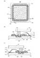
本発明の一態様について、図1を用いて説明を行う。また、図1(A)は、照明装置100の上面図を示しており、図1(B)は、図1(A)に示した破線A1−A2に相当する断面図を示しており、図1(C)は、図1(A)に示した破線A2−A3に相当する断面図を示している。なお、図1(A)においては、構成要素の一部(例えば、封止基板118など)を図面が煩雑になることを避け、省略している。(Embodiment 1)
One embodiment of the present invention will be described with reference to FIGS. 1A illustrates a top view of the
図1(A)乃至図1(C)に示す照明装置100は、基板102と、基板102上に形成された凹凸領域120と、基板102上に形成された第1の電極104と、基板102、凹凸領域120、及び第1の電極104上に形成された接続電極106と、第1の電極104及び接続電極106を覆う隔壁108と、第1の電極104、及び隔壁108上に形成された発光層110と、隔壁108、発光層110、及び接続電極106上に形成された第2の電極112と、基板102と対向して設けられた封止基板118と、基板102と封止基板118を封止するシール材116と、を有している。 A
なお、照明装置100は、基板102側に発光が取り出される下面射出型(所謂ボトムエミッション型)の照明装置である。そのため、基板102、及び第1の電極104は、透光性の材料を用いる。ただし、本発明はこれに限定されない。例えば、封止基板118側に発光が取り出される上面射出型(所謂トップエミッション型)の照明装置、または、基板102、及び封止基板118両方から発光が取り出される両面射出型(所謂デュアルエミッション型)の照明装置としても良い。なお、発光が取り出される側には、透光性の材料を用いる。 Note that the
また、第1の電極104、発光層110、及び第2の電極112により発光素子114が形成されている。発光素子114は、第1の電極104と、第2の電極112との間に電圧を印加することにより、発光層110からの発光を得ることができる。なお、第1の電極104、及び第2の電極112は、それぞれ接続電極106と接続され、第1の電極104と接続する接続電極106と、第2の電極112と接続する接続電極106との間に電圧を印加する。すなわち、接続電極106は、外部からの入力端子電極としても機能する。 In addition, a light-emitting
また、第1の電極104は、透光性を有する導電膜である。ところが、この透光性を有する導電膜は、電気を流しやすい金属などと比較して、一桁から二桁比抵抗率が高く、発光素子114の面積が大きい場合、電圧降下による発光素子114面内の輝度変化が顕著である。したがって、接続電極106は、第1の電極104よりも抵抗が低い方が好ましい。このように、第1の電極104は、接続電極106を介して外部に取り出される。このような構成とすることで、発光素子114に均一に電圧を供給することができる。また、接続電極106は、第1の電極104の補助配線としての機能も有する。例えば、接続電極106の形状が、平面においてストライプ状、または横縞状等とし、発光素子114が形成される領域を分断するような構造とすることで、さらに電圧降下による発光素子114の輝度変化を抑制することができるので、好適である。なお、このような構成とする場合においては、接続電極106は、第1の電極104と接して設け、接続電極106上に隔壁108を設けて、第2の電極112と絶縁される構造とする。 The
また、シール材116は、発光素子114の外周を囲んで形成され、基板102に形成された凹凸領域120、及び凹凸領域120上に形成された接続電極106と接して、基板102と封止基板118と、が接着されている。 The
なお、接続電極106は、スクリーン印刷法等を用いて形成された導電性ペーストを用いることができる。凹凸領域120上に接続電極を形成するために、例えばスパッタリング法などを用いて導電膜を形成した場合、凹凸領域120により導電膜が断線する可能性がある。しかし、導電性ペーストは、流動性、粘性に優れ、凹凸領域120内に導電性粒子が入り込み、さらに、凹凸領域120の形状を転写することができる。また、導電性ペーストが含有している導電性粒子により、接続電極106の表面が粗面化されるため、シール材116との接着面積が増大することで、密着性が向上し非常に好適である。なお、図1(B)、及び図1(C)において、接続電極106は、複数の導電性粒子(図中では、円形状)により形成された構成を模式的に示している。 Note that the
このように、シール材116の封止領域は、基板102に形成された凹凸領域120、及び凹凸領域120上に形成された接続電極106と接する。凹凸領域120、及び凹凸領域120上に形成された接続電極106により、シール材116の接着面積が増加し、外部からの水分、酸素などの成分が発光素子114内部への侵入を抑制することができる。また、接続電極106は、導電性ペーストにより形成されており、導電性ペーストが含有している導電性粒子により、表面が粗面化されている。そのため、凹凸領域120、及び接続電極106により、優れた封止構造とすることができる。 As described above, the sealing region of the sealing
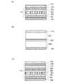
ここで、図2、及び図3を用いて、図1に示す照明装置100の作製方法について説明を行う。 Here, a method for manufacturing the
なお、図2(A)、図2(B)、及び図2(C)においては、照明装置100の上面図を示しており、図2(D)、図2(E)、及び図2(F)は、図2(A)、図2(B)、及び図2(C)に示す破線A1−A2に相当する断面図を各々示している。また、図3(A)、及び図3(B)においては、照明装置100の上面図を示しており、図3(C)、及び図3(E)は、図3(A)、及び図3(B)に示す破線A1−A2に相当する断面図を各々示しており、図3(D)、及び図3(F)は、図3(A)、及び図3(B)に示す破線A2−A3に相当する断面図を各々示している。なお、図2においては、破線A2−A3の断面図は省略している。 2A, 2B, and 2C are top views of the
まず、基板102上に凹凸領域120を形成する。凹凸領域120は、所望の領域にショットブラスト、サンドブラスト、化学エッチングなどを行うことにより凹部(または溝)として形成することができ、凹部に凹凸な表面を有している。なお、本実施の形態においては、発光素子114(のちに形成される)の外周領域を囲んで凹凸領域120を形成する。次に、基板102の凹凸領域120の内側に第1の電極104を形成する。(図2(A)、及び図2(D)参照)。 First, the
基板102としては、ガラス基板、石英基板、有機樹脂、プラスティック基板などの透光性を有する材料を用いることができる。基板102として有機樹脂を用いる場合、有機樹脂としては、例えば、ポリエチレンテレフタレート(PET)、ポリエチレンナフタレート(PEN)等のポリエステル樹脂、ポリアクリルニトリル樹脂、ポリイミド樹脂、ポリメチルメタクリレート樹脂、ポリカーボネート(PC)樹脂、ポリエーテルスルフォン(PES)樹脂、ポリアミド樹脂、シクロオレフィン樹脂、ポリスチレン樹脂、ポリアミドイミド樹脂、またはポリ塩化ビニル樹脂などを用いることができる。また、ガラス繊維に有機樹脂を含浸した基板や、無機フィラーを有機樹脂に混ぜた基板を使用することもできる。 As the
また、基板102と第1の電極104の間に下地絶縁膜を形成してもよい。下地絶縁膜は、基板102からの水分や酸素などの不純物の拡散を防止するパッシベーション膜としての機能を有する膜を形成することができる。下地絶縁膜は、その材料に応じて、スパッタリング法やCVD法などの堆積法、ディップ法、スピンコート法、インクジェット法などの塗布法、スクリーン印刷法などの印刷法などを適宜用いればよい。 Further, a base insulating film may be formed between the
第1の電極104としては、スパッタリング法などの成膜方法を用いて、透光性の導電膜を形成する。なお、スパッタリング時にメタルマスク(シャドーマスクともいう)を用いて、所望の領域に透光性の導電膜を形成することができる。例えば、第1の電極104に用いることのできる材料としては、酸化インジウム、酸化インジウム酸化スズ(ITO)、酸化インジウム酸化亜鉛、酸化亜鉛、ガリウムを添加した酸化亜鉛、グラフェンなどを用いることができる。 As the
また、第1の電極104として、金、銀、白金、マグネシウム、ニッケル、タングステン、クロム、モリブデン、鉄、コバルト、銅、パラジウム、又はチタン等の金属材料や、これらの合金を用いることができる。または、それら金属材料の窒化物(例えば、窒化チタン)等を用いてもよい。なお、金属材料(又はその窒化物)を用いる場合、透光性を有する程度に薄くすればよい。 As the
また、上記材料の積層膜を第1の電極104として用いることができる。例えば、銀とマグネシウムの合金とITOとの積層膜などを用いると、導電性を高めることができるため好ましい。 In addition, a stacked film of the above materials can be used as the
なお、透光性の導電膜を基板102の全面に形成し、その後、フォトリソグラフィ法などの公知のパターニング技術を用いて、当該透光性の導電膜の不要な部分を除去し、第1の電極104とすることもできる。ただし、上述した通り、好ましくはスパッタリング時にメタルマスクを用いて、所望の領域に透光性の導電膜を形成する。このように、フォトリソグラフィによるパターニングプロセスを行わずに、メタルマスクによる蒸着法、スクリーン印刷法などによってパターンを形成することにより、より簡素化された方法で照明装置を作製することができる。 Note that a light-transmitting conductive film is formed over the entire surface of the
次に、基板102、第1の電極104、及び凹凸領域120上に接続電極106を形成する(図2(B)、及び図2(E)参照)。 Next, the
接続電極106としては、スクリーン印刷法、インクジェット法等により形成可能な導電性ペーストを用いる。導電性ペーストは、特に銀粒子をフィラーとして含有した銀ペースト、または銅粒子をフィラーとして含有した銅ペーストを用いると好適である。銀ペースト、または銅ペーストは、第1の電極104よりも比抵抗率を低くすることができるため、電圧降下を抑制することができる。 As the
次に、第1の電極104、及び接続電極106上に隔壁108を形成する(図2(C)、及び図2(F)参照)。 Next, a
隔壁108は、第1の電極104、及び接続電極106の端部を覆っている。すなわち、隔壁108は、当該端部の段差によって、発光層110(のちに形成される)が分断され、当該端部の段差で第1の電極104と、第2の電極112と、が短絡することを抑制するために設けられる。なお、隔壁108は、不要であれば設けない構成としても良い。 The
隔壁108としては、印刷法、インクジェット法を用い、感光性樹脂を形成する。例えば、ポリイミド樹脂、アクリル樹脂、ポリアミド樹脂、エポキシ樹脂等の有機樹脂、または無機絶縁材料を用いることができる。特に感光性の樹脂材料を用いて開口部を形成し、その開口部の側壁が連続した曲率を持って形成される傾斜面となるように形成することが好ましい。具体的には、隔壁108の断面が描いている曲線の曲率半径が、0.2〜2μm程度であることが望ましい。隔壁108の形成方法は、特に限定されないが、スパッタリング法、蒸着法、スクリーン印刷法やオフセット印刷法などの印刷法、インクジェット法やディスペンス法などの液滴吐出法、スリットコート法やスピンコート法などの塗布法などを用いればよい。 As the
次に、第1の電極104、及び隔壁108上に発光層110を形成し、その後、隔壁108、発光層110、及び接続電極106上に第2の電極112を形成する。なお、第1の電極104、発光層110、及び第2の電極112によって、発光素子114が形成される(図3(A)、図3(C)、及び図3(D)参照)。 Next, the light-emitting
本実施の形態においては、発光層110を蒸着法により形成した後、隔壁108、発光層110、及び接続電極106と重なる領域上に第2の電極112を蒸着法により形成する。なお、発光層110、及び第2の電極112は、各々所望の領域に形成するために、メタルマスクを用いて形成する。 In this embodiment, after the light-emitting
発光層110としては、少なくとも発光性の有機化合物を含む層を有する。そのほか、電子輸送性の高い物質を含む層、正孔輸送性の高い物質を含む層、電子注入性の高い物質を含む層、正孔注入性の高い物質を含む層、バイポーラ性の物質(電子輸送性及び正孔輸送性が高い物質)を含む層等を適宜組み合わせた積層構造を構成することができる。 The light-emitting
第2の電極112としては、反射性を有する材料を用いて形成する。反射性を有する材料としては、アルミニウム、金、白金、銀、ニッケル、タングステン、クロム、モリブデン、鉄、コバルト、銅、ランタン、又はパラジウム等の金属材料を含む金属又は合金を用いることができる。そのほか、アルミニウムとチタンの合金、アルミニウムとニッケルの合金、アルミニウムとネオジムの合金などのアルミニウムを含む合金(アルミニウム合金)や銀と銅の合金、銀とマグネシウムの合金などの銀を含む合金を用いることもできる。銀と銅の合金は、耐熱性が高いため好ましい。さらに、アルミニウム合金膜に接する金属膜、又は金属酸化物膜を積層することでアルミニウム合金膜の酸化を抑制することができる。該金属膜、金属酸化物膜の材料としては、チタン、酸化チタンなどが挙げられる。 The
また、第2の電極112を形成したあと、発光素子114を覆う保護膜、及びシート状のシール材による固体封止などを行ってもよい。固体封止により、発光素子114への水分、酸素などの不純物の浸入を抑制し、信頼性の高い照明装置とすることができる。 Further, after the
以上の工程で基板102上に形成された発光素子114を形成することができる。 Through the above steps, the light-emitting
次に、シール材116を用いて、発光素子114が形成された基板102と、対向して封止基板118を貼り合わせる(図3(B)、図3(E)、及び図3(F)参照)。 Next, the sealing
また、発光素子114と封止基板118との間の空間内に乾燥剤や吸着剤を備えると好ましい。当該乾燥剤や吸着剤によって、封止領域内部の水分、酸素などの不純物が低減されるため、発光素子114の劣化が抑制され、信頼性の高い照明装置とすることができる。 In addition, a desiccant or an adsorbent is preferably provided in the space between the light emitting
シール材116は、発光素子114の外周を囲むように設けられ、基板102に形成された凹凸領域120、及び当該凹凸領域120上に形成された接続電極106と接する。 The sealing
シール材116は、例えばスクリーン印刷などの印刷法や、ディスペンス法などの塗布法を用いて形成することができる。また、シール材116に用いることのできる材料としては、公知の材料を用いることができる。例えば、熱硬化型の樹脂材料、紫外線硬化型の樹脂材料、または、低融点ガラス材料(フリットガラス)を用いても良い。また二液混合型のエポキシ樹脂などを用いることができる。また、シール材に用いる材料はできるだけ水分や酸素を透過しない材料であることが望ましい。またシール材には乾燥剤が含まれていても良い。例えば、アルカリ土類金属の酸化物(酸化カルシウムや酸化バリウム等)のように、化学吸着によって水分を吸収する物質を用いることができる。その他の乾燥剤として、ゼオライトやシリカゲル等のように、物理吸着によって水分を吸着する物質を用いてもよい。 The sealing
なお、本実施の形態において、シール材116は、封止基板118側に塗布し、基板102と貼り合わせる。ただし、本発明はこれに限定されず、基板102側にシール材116を形成しても良い。 Note that in this embodiment, the
貼り合わせ方法としては、まず、封止基板118上にシール材116を塗布する。次に、封止基板118と、基板102のアライメントを行い、基板102上に形成された凹凸領域120、及び凹凸領域120上に形成された接続電極106と、シール材116を接着させる。その後、圧力をかけながら基板102と封止基板118を貼り合わせ、熱や紫外線の照射によりシール材116を硬化する。 As a bonding method, first, the sealing
貼り合わせ工程は、減圧雰囲気、または不活性雰囲気下で行い、水や酸素などの不純物ができるだけ低減された雰囲気下で行うことが好ましい。このような雰囲気下で貼り合わせを行うことにより、基板102と封止基板118との間の空間内に含まれる水や酸素などの不純物を低減することができ、信頼性の高い照明装置100を作製することができる。当該貼り合わせ工程によりシール材116が硬化し、基板102と封止基板118とが当該シール材116によって接着される。 The bonding step is preferably performed in a reduced-pressure atmosphere or an inert atmosphere, and in an atmosphere in which impurities such as water and oxygen are reduced as much as possible. By bonding in such an atmosphere, impurities such as water and oxygen contained in the space between the
封止基板118としては、基板102と同様な材料を用いることができる。ただし、封止基板118は、透光性を有する必要が無いため、金属基板などの熱伝導性の高い基板を用いることが好ましい。発光素子114を用いた大型の照明装置の場合、発光素子114からの発熱が問題となる場合があるため、このような熱伝導性の高い基板を用いると放熱性が高まる。例えば、ステンレス基板、アルミニウム酸化物、ジュラルミンなどを用いると、軽量且つ放熱性を高めることができる。 As the sealing
また、封止基板118のシール材116が形成される領域は、基板102のシール材116が形成される領域と同様な構成としても良い。すなわち、封止基板118側にも凹凸領域、及び導電性ペーストを形成しても良い。 Further, the region where the sealing
以上の工程で図1に示す照明装置100を形成することできる。このように、フォトリソグラフィによるパターニングプロセスを行わずに、メタルマスクによる蒸着法、スクリーン印刷法などによってパターンを形成することにより、より簡素化された方法で照明装置を作製することができる。 Through the above steps, the
また、封止領域において、シール材116は、基板102に形成された凹凸領域120、及び凹凸領域120上に形成された接続電極106と接する。このように、シール材116は、発光素子114の外周に形成された凹凸領域120、及び凹凸領域120上に形成された接続電極106と接することで、接着面積が向上し、密着性を高めることができる。なお、接続電極106は、導電性ペーストにより形成されており、導電性ペーストが含有している導電性粒子により表面が粗面化されているため、接着面積を向上させ、優れた封止構造とすることができる。 In the sealing region, the sealing
本実施の形態は、他の実施の形態と適宜組み合わせて実施することができる。 This embodiment can be implemented in appropriate combination with any of the other embodiments.
(実施の形態2)
本実施の形態においては、先の実施の形態1に示した照明装置100と異なる形態について、図4を用いて説明を行う。なお、図1で用いた符号と同様の箇所には同様の符号を用い、その説明は省略する。(Embodiment 2)
In this embodiment, a mode different from the
図4(A)は、照明装置200の上面図を示しており、図4(B)は、図4(A)に示した破線B1−B2に相当する断面図を示しており、図4(C)は、図4(A)に示した破線B2−B3に相当する断面図を示している。なお、図4(A)においては、構成要素の一部(例えば、封止基板118など)を図面が煩雑になることを避け、省略している。 4A illustrates a top view of the
図4(A)乃至図4(C)に示す照明装置200は、基板102と、マイクロレンズアレイ基板124と、基板102上に形成された凹凸領域120aと、基板102上に形成された平坦化樹脂122と、平坦化樹脂122上に形成された第1の電極104と、基板102、平坦化樹脂122、及び第1の電極104上に形成された接続電極106と、第1の電極104、及び接続電極106を覆う隔壁108と、第1の電極104、及び隔壁108上に形成された発光層110と、隔壁108、発光層110、及び接続電極106上に形成された第2の電極112と、基板102と対向して設けられた封止基板118と、基板102と封止基板118を封止するシール材116と、を有している。 The
なお、照明装置200は、基板102側に発光が取り出される下方射出型(所謂ボトムエミッション型)の照明装置である。そのため、マイクロレンズアレイ基板124、基板102、平坦化樹脂122、及び第1の電極104は、透光性の材料を用いる。 Note that the
また、第1の電極104、発光層110、及び第2の電極112により発光素子114が形成されている。発光素子114は、第1の電極104と、第2の電極112との間に電圧を印加することにより、発光層110からの発光を得ることができる。なお、第1の電極104、及び第2の電極112は、それぞれ接続電極106と接続され、第1の電極104と接続する接続電極106と、第2の電極112と接続する接続電極106との間に電圧を印加する。すなわち、接続電極106は、外部からの入力端子電極としても機能する。 In addition, a light-emitting
また、第1の電極104は、透光性を有する導電膜である。ところが、この透光性を有する導電膜は、電気を流しやすい金属などと比較して、一桁から二桁比抵抗率が高く、発光素子114の面積が大きい場合、電圧降下による発光素子114面内の輝度変化が顕著である。したがって、接続電極106は、第1の電極104よりも抵抗が低い方が好ましい。このように、第1の電極104は、接続電極106を介して外部に取り出される。このような構成とすることで、発光素子114に均一に電圧を供給することができる。また、接続電極106は、第1の電極104の補助配線としての機能も有する。例えば、接続電極106の形状が、平面においてストライプ状、または横縞状等とし、発光素子114が形成される領域を分断するような構造とすることで、さらに電圧降下による発光素子114の輝度変化を抑制することができるので、好適である。なお、このような構成とする場合においては、接続電極106は、第1の電極104と接して設け、接続電極106上に隔壁108を設けて、第2の電極112と絶縁される構造とする。 The
また、シール材116は、発光素子114の外周を囲んで形成され、基板102に形成された凹凸領域120a、及び凹凸領域120a上に形成された接続電極106と接して、基板102と封止基板118と、が接着されている。 In addition, the
なお、接続電極106は、スクリーン印刷法等を用いて形成された導電性ペーストを用いることができる。凹凸領域120a上に接続電極を形成するために、例えばスパッタリング法などを用いて導電膜を形成した場合、凹凸領域120aにより導電膜が断線する可能性がある。しかし、導電性ペーストは、流動性、粘性に優れ、凹凸領域120a内に導電性粒子が入り込み、さらに、凹凸領域120aの形状を転写することができる。また、導電性ペーストが含有している導電性粒子により、接続電極106の表面が粗面化されるため、非常に好適である。なお、図4(B)、及び図4(C)において、接続電極106は、複数の導電性粒子(図中では、円形状)により形成された構成を模式的に示している。 Note that the
なお、本実施の形態に示す照明装置200は、実施の形態1で示した照明装置100との異なる構造として、基板102に形成された凹凸領域120a、平坦化樹脂122、及びマイクロレンズアレイ基板124が挙げられる。 Note that the
基板102に形成された凹凸領域120aは、先の実施の形態1に示した凹凸領域120と同様の手法により形成することができる。ただし、基板102の片面の全てに設けることで、凹凸領域120aとすることができる。 The
なお、シール材116と接する領域においては、凹凸領域120aにより表面が粗面化され、表面積を向上させるために設けられる点については、実施の形態1に示した照明装置100と同様の効果を有するが、発光素子114の下方に設けられた凹凸領域120aは、発光素子114からの射出された光を拡散する効果を有する。 Note that, in the region in contact with the
また、発光素子114の下方に設けられた凹凸領域120a上には、平坦化樹脂122が形成されている。平坦化樹脂122は、発光層110より高い屈折率、例えば屈折率=1.6〜2.0とすることが好ましい。更に好ましくは、屈折率=1.7〜1.9とする。このような構成とすることにより、発光素子114から取り出された光は、平坦化樹脂122との界面での全反射が抑制され、平坦化樹脂122内に進入することができる。また、平坦化樹脂122内に進入した光は、基板102に形成された凹凸領域120aにより、平坦化樹脂122の下方側の界面での全反射が抑制され、マイクロレンズアレイ基板124に進入する。 Further, a
平坦化樹脂122としては、例えば、スクリーン印刷法などを用い、ポリイミド樹脂、ポリアミド樹脂、ポリイミドアミド樹脂、アクリル樹脂、BCB(ベンゾシクロブテン)などを平坦化層として用いることができる。 As the
マイクロレンズアレイ基板124は、複数の凹凸形状を有する例である。複数の凹凸形状(凸部)を有する構成とすることで、基板102と大気との界面で全反射を抑制することができるため、発光素子114からの発光の取り出し効率を向上させることができる。 The
マイクロレンズアレイ基板124は、材料として有機樹脂を用いて形成することが可能である。有機樹脂の形状は、当該有機樹脂の特性に応じて加熱処理や光照射処理を行って加工することができる。例えば、材料として熱可塑性の有機樹脂を用いて、凹凸形状(凹部)を有する支持体を用意し、加熱処理を行いながら支持体に押圧して支持体の形状を反映するように変形させ、その後冷却して硬化を行うことで、マイクロレンズアレイ基板124を形成することできる。 The
マイクロレンズアレイ基板124として、用いることのできる有機樹脂は、プラスティックが挙げられる。プラスティックとしては、例えば、ポリカーボネート、ポリアリレート、ポリエーテルスルフォン等からなる部材が挙げられる。 An example of an organic resin that can be used as the
ここで、図4に示したマイクロレンズアレイ基板124として、用いることのできる一例について、図5を用いて説明する。図5(C)、及び図5(D)は、マイクロレンズアレイ基板124a、及びマイクロレンズアレイ基板124bの平面図の一例である。図5(A)は、図5(C)の破線X1−Y1に相当する断面図を示し、図5(B)は、図5(D)の破線X2−Y2に相当する断面図を示している。 Here, an example that can be used as the
図5(A)、及び図5(C)に示すマイクロレンズアレイ基板124aは、半円形状の凹凸形状を有する。また、図5(B)、及び図5(D)に示すマイクロレンズアレイ基板124bは、底面が正六角形状の凹凸形状を有する。マイクロレンズアレイ基板124a及びマイクロレンズアレイ基板124bの有する複数の凹凸形状のピッチ、又は底面形状は様々に設定することが可能であり、図5の構成に限定されない。例えば、円錐、角錐(三角錐、四角錐等)等の頂点を有する凹凸形状としてもよい。但し、図5(B)、及び図5(D)に示すように、底面が正六角形状の凹凸形状として凹凸形状を所謂ハニカム構造とすることで、凹凸形状の充填密度を向上させることができ、外部への光の取り出し効率がより向上するため好ましい。 A
以上のように、本実施の形態に示す照明装置200は、凹凸領域120aを設けることによって、シール材116の封止領域、及び発光素子114からの光拡散効果を有する構造を同時に形成することができる。 As described above, the
また、封止領域において、シール材116は、基板102に形成された凹凸領域120a、及び凹凸領域120a上に形成された接続電極106と接する。このように、シール材116は、発光素子114の外周の凹凸領域120a、及び凹凸領域120a上に形成された接続電極106と接することで、接着面積が向上し、密着性を高めることができる。なお、接続電極106は、導電性ペーストにより形成されており、導電性ペーストが含有している導電性粒子により表面が粗面化されているため、接着面積を向上させ、優れた封止構造とすることができる。 In the sealing region, the sealing
本実施の形態は、他の実施の形態と適宜組み合わせて実施することができる。 This embodiment can be implemented in appropriate combination with any of the other embodiments.
(実施の形態3)
本実施の形態では、本発明の一態様である照明装置に用いる有機EL発光を呈する発光素子の素子構造の一例について説明する。有機EL発光を呈する発光素子は、LEDと比較して発熱が小さい。したがって、筐体として有機樹脂を用いることができるため、照明装置として軽量化が可能となり、好ましい。(Embodiment 3)
In this embodiment, an example of an element structure of a light-emitting element that emits organic EL light used for the lighting device which is one embodiment of the present invention will be described. A light emitting element that exhibits organic EL light emission generates less heat than an LED. Accordingly, an organic resin can be used for the housing, which is preferable because the lighting device can be reduced in weight.
図6(A)に示す発光素子は、第1電極104と、第1電極104上に発光層110と、発光層110上に、第2電極112を有する。 A light-emitting element illustrated in FIG. 6A includes a
発光層110は、少なくとも発光性の有機化合物を含む発光層が含まれていれば良い。そのほか、電子輸送性の高い物質を含む層、正孔輸送性の高い物質を含む層、電子注入性の高い物質を含む層、正孔注入性の高い物質を含む層、バイポーラ性の物質(電子輸送性及び正孔輸送性が高い物質)を含む層等を適宜組み合わせた積層構造を構成することができる。本実施の形態において、発光層110は、第1電極104側から、正孔注入層701、正孔輸送層702、発光層703、電子輸送層704、及び電子注入層705の順で積層されている。 The
図6(A)に示す発光素子の作製方法について説明する。 A method for manufacturing the light-emitting element illustrated in FIG. 6A will be described.
まず、第1電極104を形成する。第1電極104は、発光層110から見て、光の取り出し方向に設けられるため、透光性を有する材料を用いて形成する。 First, the
透光性を有する材料としては、酸化インジウム、酸化インジウム酸化スズ(ITOともいう)、酸化インジウム酸化亜鉛、酸化亜鉛、ガリウムを添加した酸化亜鉛、グラフェンなどを用いることができる。 As the light-transmitting material, indium oxide, indium tin oxide (also referred to as ITO), indium zinc oxide, zinc oxide, zinc oxide to which gallium is added, graphene, or the like can be used.
また、第1電極104として、金、白金、ニッケル、タングステン、クロム、モリブデン、鉄、コバルト、銅、パラジウム、又はチタン等の金属材料を用いることができる。または、それら金属材料の窒化物(例えば、窒化チタン)等を用いてもよい。なお、金属材料(又はその窒化物)を用いる場合、透光性を有する程度に薄くすればよい。 As the
次に、第1電極104上に、発光層110を形成する。本実施の形態において、発光層110は、正孔注入層701、正孔輸送層702、発光層703、電子輸送層704、及び電子注入層705を有する。 Next, the
正孔注入層701は、正孔注入性の高い物質を含む層である。正孔注入性の高い物質としては、例えば、モリブデン酸化物、チタン酸化物、バナジウム酸化物、レニウム酸化物、ルテニウム酸化物、クロム酸化物、ジルコニウム酸化物、ハフニウム酸化物、タンタル酸化物、銀酸化物、タングステン酸化物、マンガン酸化物等の金属酸化物を用いることができる。また、フタロシアニン(略称:H2Pc)、銅(II)フタロシアニン(略称:CuPc)等のフタロシアニン系の化合物を用いることができる。The
また、低分子の有機化合物である4,4’,4’’−トリス(N,N−ジフェニルアミノ)トリフェニルアミン(略称:TDATA)、4,4’,4’’−トリス[N−(3−メチルフェニル)−N−フェニルアミノ]トリフェニルアミン(略称:MTDATA)、4,4’−ビス[N−(4−ジフェニルアミノフェニル)−N−フェニルアミノ]ビフェニル(略称:DPAB)、4,4’−ビス(N−{4−[N’−(3−メチルフェニル)−N’−フェニルアミノ]フェニル}−N−フェニルアミノ)ビフェニル(略称:DNTPD)、1,3,5−トリス[N−(4−ジフェニルアミノフェニル)−N−フェニルアミノ]ベンゼン(略称:DPA3B)、3−[N−(9−フェニルカルバゾール−3−イル)−N−フェニルアミノ]−9−フェニルカルバゾール(略称:PCzPCA1)、3,6−ビス[N−(9−フェニルカルバゾール−3−イル)−N−フェニルアミノ]−9−フェニルカルバゾール(略称:PCzPCA2)、3−[N−(1−ナフチル)−N−(9−フェニルカルバゾール−3−イル)アミノ]−9−フェニルカルバゾール(略称:PCzPCN1)等の芳香族アミン化合物等を用いることができる。 In addition, 4,4 ′, 4 ″ -tris (N, N-diphenylamino) triphenylamine (abbreviation: TDATA), 4,4 ′, 4 ″ -tris [N- ( 3-methylphenyl) -N-phenylamino] triphenylamine (abbreviation: MTDATA), 4,4′-bis [N- (4-diphenylaminophenyl) -N-phenylamino] biphenyl (abbreviation: DPAB), 4 , 4′-bis (N- {4- [N ′-(3-methylphenyl) -N′-phenylamino] phenyl} -N-phenylamino) biphenyl (abbreviation: DNTPD), 1,3,5-tris [N- (4-diphenylaminophenyl) -N-phenylamino] benzene (abbreviation: DPA3B), 3- [N- (9-phenylcarbazol-3-yl) -N-phenylamino]- -Phenylcarbazole (abbreviation: PCzPCA1), 3,6-bis [N- (9-phenylcarbazol-3-yl) -N-phenylamino] -9-phenylcarbazole (abbreviation: PCzPCA2), 3- [N- ( An aromatic amine compound such as 1-naphthyl) -N- (9-phenylcarbazol-3-yl) amino] -9-phenylcarbazole (abbreviation: PCzPCN1) can be used.
さらに、高分子化合物(オリゴマー、デンドリマー、ポリマー等)を用いることもできる。例えば、ポリ(N−ビニルカルバゾール)(略称:PVK)、ポリ(4−ビニルトリフェニルアミン)(略称:PVTPA)、ポリ[N−(4−{N’−[4−(4−ジフェニルアミノ)フェニル]フェニル−N’−フェニルアミノ}フェニル)メタクリルアミド](略称:PTPDMA)、ポリ[N,N’−ビス(4−ブチルフェニル)−N,N’−ビス(フェニル)ベンジジン](略称:Poly−TPD)などの高分子化合物が挙げられる。また、ポリ(3,4−エチレンジオキシチオフェン)/ポリ(スチレンスルホン酸)(PEDOT/PSS)、ポリアニリン/ポリ(スチレンスルホン酸)(PAni/PSS)等の酸を添加した高分子化合物を用いることができる。 Furthermore, a high molecular compound (an oligomer, a dendrimer, a polymer, etc.) can also be used. For example, poly (N-vinylcarbazole) (abbreviation: PVK), poly (4-vinyltriphenylamine) (abbreviation: PVTPA), poly [N- (4- {N ′-[4- (4-diphenylamino)] Phenyl] phenyl-N′-phenylamino} phenyl) methacrylamide] (abbreviation: PTPDMA), poly [N, N′-bis (4-butylphenyl) -N, N′-bis (phenyl) benzidine] (abbreviation: Polymer compounds such as Poly-TPD). In addition, a polymer compound to which an acid such as poly (3,4-ethylenedioxythiophene) / poly (styrenesulfonic acid) (PEDOT / PSS), polyaniline / poly (styrenesulfonic acid) (PAni / PSS) is added is used. be able to.
特に、正孔注入層701として、正孔輸送性の高い有機化合物にアクセプター性物質を含有させた複合材料を用いることが好ましい。正孔輸送性の高い物質にアクセプター性物質を含有させた複合材料を用いることにより、第1電極104からの正孔注入性を良好にし、発光素子の駆動電圧を低減することができる。これらの複合材料は、正孔輸送性の高い物質とアクセプター物質とを共蒸着することにより形成することができる。該複合材料を用いて正孔注入層701を形成することにより、第1電極104から発光層110への正孔注入が容易となる。 In particular, for the hole-injecting
複合材料に用いる有機化合物としては、芳香族アミン化合物、カルバゾール誘導体、芳香族炭化水素、高分子化合物(オリゴマー、デンドリマー、ポリマー等)など、種々の化合物を用いることができる。なお、複合材料に用いる有機化合物としては、正孔輸送性の高い有機化合物であることが好ましい。具体的には、10−6cm2/Vs以上の正孔移動度を有する物質であることが好ましい。但し、電子よりも正孔の輸送性の高い物質であれば、これら以外のものを用いてもよい。以下では、複合材料に用いることのできる有機化合物を具体的に列挙する。As the organic compound used for the composite material, various compounds such as an aromatic amine compound, a carbazole derivative, an aromatic hydrocarbon, and a high molecular compound (such as an oligomer, a dendrimer, and a polymer) can be used. Note that the organic compound used for the composite material is preferably an organic compound having a high hole-transport property. Specifically, a substance having a hole mobility of 10−6 cm2 / Vs or higher is preferable. Note that other than these substances, any substance that has a property of transporting more holes than electrons may be used. Below, the organic compound which can be used for a composite material is listed concretely.
複合材料に用いることのできる有機化合物としては、例えば、TDATA、MTDATA、DPAB、DNTPD、DPA3B、PCzPCA1、PCzPCA2、PCzPCN1、4,4’−ビス[N−(1−ナフチル)−N−フェニルアミノ]ビフェニル(略称:NPB又はα−NPD)、N,N’−ビス(3−メチルフェニル)−N,N’−ジフェニル−[1,1’−ビフェニル]−4,4’−ジアミン(略称:TPD)、4−フェニル−4’−(9−フェニルフルオレン−9−イル)トリフェニルアミン(略称:BPAFLP)等の芳香族アミン化合物や、4,4’−ジ(N−カルバゾリル)ビフェニル(略称:CBP)、1,3,5−トリス[4−(N−カルバゾリル)フェニル]ベンゼン(略称:TCPB)、9−[4−(10−フェニル−9−アントリル)フェニル]−9H−カルバゾール(略称:CzPA)、9−フェニル−3−[4−(10−フェニル−9−アントリル)フェニル]−9H−カルバゾール(略称:PCzPA)、1,4−ビス[4−(N−カルバゾリル)フェニル]−2,3,5,6−テトラフェニルベンゼン等のカルバゾール誘導体を用いることができる。 Examples of an organic compound that can be used for the composite material include TDATA, MTDATA, DPAB, DNTPD, DPA3B, PCzPCA1, PCzPCA2, PCzPCN1, 4,4′-bis [N- (1-naphthyl) -N-phenylamino]. Biphenyl (abbreviation: NPB or α-NPD), N, N′-bis (3-methylphenyl) -N, N′-diphenyl- [1,1′-biphenyl] -4,4′-diamine (abbreviation: TPD) ), 4-phenyl-4 ′-(9-phenylfluoren-9-yl) triphenylamine (abbreviation: BPAFLP) and the like, and 4,4′-di (N-carbazolyl) biphenyl (abbreviation: CBP), 1,3,5-tris [4- (N-carbazolyl) phenyl] benzene (abbreviation: TCPB), 9- [4- (10 Phenyl-9-anthryl) phenyl] -9H-carbazole (abbreviation: CzPA), 9-phenyl-3- [4- (10-phenyl-9-anthryl) phenyl] -9H-carbazole (abbreviation: PCzPA), 1, A carbazole derivative such as 4-bis [4- (N-carbazolyl) phenyl] -2,3,5,6-tetraphenylbenzene can be used.
また、2−tert−ブチル−9,10−ジ(2−ナフチル)アントラセン(略称:t−BuDNA)、2−tert−ブチル−9,10−ジ(1−ナフチル)アントラセン、9,10−ビス(3,5−ジフェニルフェニル)アントラセン(略称:DPPA)、2−tert−ブチル−9,10−ビス(4−フェニルフェニル)アントラセン(略称:t−BuDBA)、9,10−ジ(2−ナフチル)アントラセン(略称:DNA)、9,10−ジフェニルアントラセン(略称:DPAnth)、2−tert−ブチルアントラセン(略称:t−BuAnth)、9,10−ビス(4−メチル−1−ナフチル)アントラセン(略称:DMNA)、9,10−ビス[2−(1−ナフチル)フェニル]−2−tert−ブチルアントラセン、9,10−ビス[2−(1−ナフチル)フェニル]アントラセン、2,3,6,7−テトラメチル−9,10−ジ(1−ナフチル)アントラセン等の芳香族炭化水素化合物を用いることができる。 2-tert-butyl-9,10-di (2-naphthyl) anthracene (abbreviation: t-BuDNA), 2-tert-butyl-9,10-di (1-naphthyl) anthracene, 9,10-bis (3,5-diphenylphenyl) anthracene (abbreviation: DPPA), 2-tert-butyl-9,10-bis (4-phenylphenyl) anthracene (abbreviation: t-BuDBA), 9,10-di (2-naphthyl) ) Anthracene (abbreviation: DNA), 9,10-diphenylanthracene (abbreviation: DPAnth), 2-tert-butylanthracene (abbreviation: t-BuAnth), 9,10-bis (4-methyl-1-naphthyl) anthracene ( Abbreviations: DMNA), 9,10-bis [2- (1-naphthyl) phenyl] -2-tert-butylanthracene, 9, 0- bis [2- (1-naphthyl) phenyl] anthracene, and 2,3,6,7-tetramethyl-9,10-di (1-naphthyl) aromatic hydrocarbon compounds such as anthracene.
さらに、2,3,6,7−テトラメチル−9,10−ジ(2−ナフチル)アントラセン、9,9’−ビアントリル、10,10’−ジフェニル−9,9’−ビアントリル、10,10’−ビス(2−フェニルフェニル)−9,9’−ビアントリル、10,10’−ビス[(2,3,4,5,6−ペンタフェニル)フェニル]−9,9’−ビアントリル、アントラセン、テトラセン、ルブレン、ペリレン、2,5,8,11−テトラ(tert−ブチル)ペリレン、ペンタセン、コロネン、4,4’−ビス(2,2−ジフェニルビニル)ビフェニル(略称:DPVBi)、9,10−ビス[4−(2,2−ジフェニルビニル)フェニル]アントラセン(略称:DPVPA)等の芳香族炭化水素化合物を用いることができる。 Further, 2,3,6,7-tetramethyl-9,10-di (2-naphthyl) anthracene, 9,9′-bianthryl, 10,10′-diphenyl-9,9′-bianthryl, 10,10 ′ -Bis (2-phenylphenyl) -9,9'-bianthryl, 10,10'-bis [(2,3,4,5,6-pentaphenyl) phenyl] -9,9'-bianthryl, anthracene, tetracene , Rubrene, perylene, 2,5,8,11-tetra (tert-butyl) perylene, pentacene, coronene, 4,4'-bis (2,2-diphenylvinyl) biphenyl (abbreviation: DPVBi), 9,10- An aromatic hydrocarbon compound such as bis [4- (2,2-diphenylvinyl) phenyl] anthracene (abbreviation: DPVPA) can be used.
また、電子受容体としては、7,7,8,8−テトラシアノ−2,3,5,6−テトラフルオロキノジメタン(略称:F4−TCNQ)、クロラニル等の有機化合物や、遷移金属酸化物を挙げることができる。また、元素周期表における第4族乃至第8族に属する金属の酸化物を挙げることができる。具体的には、酸化バナジウム、酸化ニオブ、酸化タンタル、酸化クロム、酸化モリブデン、酸化タングステン、酸化マンガン、酸化レニウムは電子受容性が高いため好ましい。中でも特に、酸化モリブデンは大気中でも安定であり、吸湿性が低く、扱いやすいため好ましい。Examples of the electron acceptor include organic compounds such as 7,7,8,8-tetracyano-2,3,5,6-tetrafluoroquinodimethane (abbreviation: F4 -TCNQ), chloranil, and transition metal oxidation. You can list things. In addition, oxides of metals belonging to Groups 4 to 8 in the periodic table can be given. Specifically, vanadium oxide, niobium oxide, tantalum oxide, chromium oxide, molybdenum oxide, tungsten oxide, manganese oxide, and rhenium oxide are preferable because of their high electron accepting properties. Among these, molybdenum oxide is especially preferable because it is stable in the air, has a low hygroscopic property, and is easy to handle.
なお、上述したPVK、PVTPA、PTPDMA、Poly−TPD等の高分子化合物と、上述した電子受容体を用いて複合材料を形成し、正孔注入層701に用いてもよい。 Note that a composite material may be formed using the above-described electron acceptor with a polymer compound such as PVK, PVTPA, PTPDMA, or Poly-TPD, and used for the hole-
正孔輸送層702は、正孔輸送性の高い物質を含む層である。正孔輸送性の高い物質としては、例えば、NPB、TPD、BPAFLP、4,4’−ビス[N−(9,9−ジメチルフルオレン−2−イル)−N−フェニルアミノ]ビフェニル(略称:DFLDPBi)、4,4’−ビス[N−(スピロ−9,9’−ビフルオレン−2−イル)−N―フェニルアミノ]ビフェニル(略称:BSPB)等の芳香族アミン化合物を用いることができる。ここに述べた物質は、主に10−6cm2/Vs以上の正孔移動度を有する物質である。但し、電子よりも正孔の輸送性の高い物質であれば、これら以外のものを用いてもよい。なお、正孔輸送性の高い物質を含む層は、単層のものだけでなく、上記物質からなる層が二層以上積層したものとしてもよい。The hole-
また、正孔輸送層702には、CBP、CzPA、PCzPAのようなカルバゾール誘導体や、t−BuDNA、DNA、DPAnthのようなアントラセン誘導体を用いても良い。 For the hole-
また、正孔輸送層702には、PVK、PVTPA、PTPDMA、Poly−TPDなどの高分子化合物を用いることもできる。 For the hole-
発光層703は、発光性の有機化合物を含む層である。発光性の有機化合物としては、例えば、蛍光を発光する蛍光性化合物や燐光を発光する燐光性化合物を用いることができる。 The
発光層703に用いることができる蛍光性化合物としては、例えば、青色系の発光材料として、N,N’−ビス[4−(9H−カルバゾール−9−イル)フェニル]−N,N’−ジフェニルスチルベン−4,4’−ジアミン(略称:YGA2S)、4−(9H−カルバゾール−9−イル)−4’−(10−フェニル−9−アントリル)トリフェニルアミン(略称:YGAPA)、4−(10−フェニル−9−アントリル)−4’−(9−フェニル−9H−カルバゾール−3−イル)トリフェニルアミン(略称:PCBAPA)などが挙げられる。また、緑色系の発光材料として、N−(9,10−ジフェニル−2−アントリル)−N,9−ジフェニル−9H−カルバゾール−3−アミン(略称:2PCAPA)、N−[9,10−ビス(1,1’−ビフェニル−2−イル)−2−アントリル]−N,9−ジフェニル−9H−カルバゾール−3−アミン(略称:2PCABPhA)、N−(9,10−ジフェニル−2−アントリル)−N,N’,N’−トリフェニル−1,4−フェニレンジアミン(略称:2DPAPA)、N−[9,10−ビス(1,1’−ビフェニル−2−イル)−2−アントリル]−N,N’,N’−トリフェニル−1,4−フェニレンジアミン(略称:2DPABPhA)、N−[9,10−ビス(1,1’−ビフェニル−2−イル)]−N−[4−(9H−カルバゾール−9−イル)フェニル]−N−フェニルアントラセン−2−アミン(略称:2YGABPhA)、N,N,9−トリフェニルアントラセン−9−アミン(略称:DPhAPhA)などが挙げられる。また、黄色系の発光材料として、ルブレン、5,12−ビス(1,1’−ビフェニル−4−イル)−6,11−ジフェニルテトラセン(略称:BPT)などが挙げられる。また、赤色系の発光材料として、N,N,N’,N’−テトラキス(4−メチルフェニル)テトラセン−5,11−ジアミン(略称:p−mPhTD)、7,14−ジフェニル−N,N,N’,N’−テトラキス(4−メチルフェニル)アセナフト[1,2−a]フルオランテン−3,10−ジアミン(略称:p−mPhAFD)などが挙げられる。 As a fluorescent compound that can be used for the light-emitting
また、発光層703に用いることができる燐光性化合物としては、例えば、青色系の発光材料として、ビス[2−(4’,6’−ジフルオロフェニル)ピリジナト−N,C2’]イリジウム(III)テトラキス(1−ピラゾリル)ボラート(略称:FIr6)、ビス[2−(4’,6’−ジフルオロフェニル)ピリジナト−N,C2’]イリジウム(III)ピコリナート(略称:FIrpic)、ビス{2−[3’,5’−ビス(トリフルオロメチル)フェニル]ピリジナト−N,C2’}イリジウム(III)ピコリナート(略称:Ir(CF3ppy)2(pic))、ビス[2−(4’,6’−ジフルオロフェニル)ピリジナト−N,C2’]イリジウム(III)アセチルアセトナート(略称:FIr(acac))などが挙げられる。また、緑色系の発光材料として、トリス(2−フェニルピリジナト−N,C2’)イリジウム(III)(略称:Ir(ppy)3)、ビス(2−フェニルピリジナト−N,C2’)イリジウム(III)アセチルアセトナート(略称:Ir(ppy)2(acac))、ビス(1,2−ジフェニル−1H−ベンゾイミダゾラト)イリジウム(III)アセチルアセトナート(略称:Ir(pbi)2(acac))、ビス(ベンゾ[h]キノリナト)イリジウム(III)アセチルアセトナート(略称:Ir(bzq)2(acac))、トリス(ベンゾ[h]キノリナト)イリジウム(III)(略称:Ir(bzq)3)などが挙げられる。また、黄色系の発光材料として、ビス(2,4−ジフェニル−1,3−オキサゾラト−N,C2’)イリジウム(III)アセチルアセトナート(略称:Ir(dpo)2(acac))、ビス[2−(4’−パーフルオロフェニルフェニル)ピリジナト]イリジウム(III)アセチルアセトナート(略称:Ir(p−PF−ph)2(acac))、ビス(2−フェニルベンゾチアゾラト−N,C2’)イリジウム(III)アセチルアセトナート(略称:Ir(bt)2(acac))、(アセチルアセトナト)ビス[2,3−ビス(4−フルオロフェニル)−5−メチルピラジナト]イリジウム(III)(略称:Ir(Fdppr−Me)2(acac))、(アセチルアセトナト)ビス{2−(4−メトキシフェニル)−3,5−ジメチルピラジナト}イリジウム(III)(略称:Ir(dmmoppr)2(acac))などが挙げられる。また、橙色系の発光材料として、トリス(2−フェニルキノリナト−N,C2’)イリジウム(III)(略称:Ir(pq)3)、ビス(2−フェニルキノリナト−N,C2’)イリジウム(III)アセチルアセトナート(略称:Ir(pq)2(acac))、(アセチルアセトナト)ビス(3,5−ジメチル−2−フェニルピラジナト)イリジウム(III)(略称:Ir(mppr−Me)2(acac))、(アセチルアセトナト)ビス(5−イソプロピル−3−メチル−2−フェニルピラジナト)イリジウム(III)(略称:Ir(mppr−iPr)2(acac))などが挙げられる。また、赤色系の発光材料として、ビス[2−(2’−ベンゾ[4,5−α]チエニル)ピリジナト−N,C3’]イリジウム(III)アセチルアセトナート(略称:Ir(btp)2(acac))、ビス(1−フェニルイソキノリナト−N,C2’)イリジウム(III)アセチルアセトナート(略称:Ir(piq)2(acac))、(アセチルアセトナト)ビス[2,3−ビス(4−フルオロフェニル)キノキサリナト]イリジウム(III)(略称:Ir(Fdpq)2(acac))、(アセチルアセトナト)ビス(2,3,5−トリフェニルピラジナト)イリジウム(III)(略称:Ir(tppr)2(acac))、(ジピバロイルメタナト)ビス(2,3,5−トリフェニルピラジナト)イリジウム(III)(略称:Ir(tppr)2(dpm))、2,3,7,8,12,13,17,18−オクタエチル−21H,23H−ポルフィリン白金(II)(略称:PtOEP)等の有機金属錯体が挙げられる。また、トリス(アセチルアセトナト)(モノフェナントロリン)テルビウム(III)(略称:Tb(acac)3(Phen))、トリス(1,3−ジフェニル−1,3−プロパンジオナト)(モノフェナントロリン)ユーロピウム(III)(略称:Eu(DBM)3(Phen))、トリス[1−(2−テノイル)−3,3,3−トリフルオロアセトナト](モノフェナントロリン)ユーロピウム(III)(略称:Eu(TTA)3(Phen))等の希土類金属錯体は、希土類金属イオンからの発光(異なる多重度間の電子遷移)であるため、燐光性化合物として用いることができる。Examples of phosphorescent compounds that can be used for the light-emitting
なお、発光層703としては、上述した発光性の有機化合物(ゲスト材料)を他の物質(ホスト材料)に分散させた構成としてもよい。ホスト材料としては、各種のものを用いることができ、発光性の物質よりも最低空軌道準位(LUMO準位)が高く、最高被占有軌道準位(HOMO準位)が低い物質を用いることが好ましい。 Note that the light-emitting
ホスト材料としては、具体的には、トリス(8−キノリノラト)アルミニウム(III)(略称:Alq)、トリス(4−メチル−8−キノリノラト)アルミニウム(III)(略称:Almq3)、ビス(10−ヒドロキシベンゾ[h]キノリナト)ベリリウム(II)(略称:BeBq2)、ビス(2−メチル−8−キノリノラト)(4−フェニルフェノラト)アルミニウム(III)(略称:BAlq)、ビス(8−キノリノラト)亜鉛(II)(略称:Znq)、ビス[2−(2−ベンゾオキサゾリル)フェノラト]亜鉛(II)(略称:ZnPBO)、ビス[2−(2−ベンゾチアゾリル)フェノラト]亜鉛(II)(略称:ZnBTZ)などの金属錯体、2−(4−ビフェニリル)−5−(4−tert−ブチルフェニル)−1,3,4−オキサジアゾール(略称:PBD)、1,3−ビス[5−(p−tert−ブチルフェニル)−1,3,4−オキサジアゾール−2−イル]ベンゼン(略称:OXD−7)、3−(4−ビフェニリル)−4−フェニル−5−(4−tert−ブチルフェニル)−1,2,4−トリアゾール(略称:TAZ)、2,2’,2’’−(1,3,5−ベンゼントリイル)トリス(1−フェニル−1H−ベンゾイミダゾール)(略称:TPBI)、バソフェナントロリン(略称:BPhen)、バソキュプロイン(略称:BCP)などの複素環化合物や、9−[4−(10−フェニル−9−アントリル)フェニル]−9H−カルバゾール(略称:CzPA)、3,6−ジフェニル−9−[4−(10−フェニル−9−アントリル)フェニル]−9H−カルバゾール(略称:DPCzPA)、9,10−ビス(3,5−ジフェニルフェニル)アントラセン(略称:DPPA)、9,10−ジ(2−ナフチル)アントラセン(略称:DNA)、2−tert−ブチル−9,10−ジ(2−ナフチル)アントラセン(略称:t−BuDNA)、9,9’−ビアントリル(略称:BANT)、9,9’−(スチルベン−3,3’−ジイル)ジフェナントレン(略称:DPNS)、9,9’−(スチルベン−4,4’−ジイル)ジフェナントレン(略称:DPNS2)、3,3’,3’’−(ベンゼン−1,3,5−トリイル)トリピレン(略称:TPB3)、9,10−ジフェニルアントラセン(略称:DPAnth)、6,12−ジメトキシ−5,11−ジフェニルクリセンなどの縮合芳香族化合物、N,N−ジフェニル−9−[4−(10−フェニル−9−アントリル)フェニル]−9H−カルバゾール−3−アミン(略称:CzA1PA)、4−(10−フェニル−9−アントリル)トリフェニルアミン(略称:DPhPA)、N,9−ジフェニル−N−[4−(10−フェニル−9−アントリル)フェニル]−9H−カルバゾール−3−アミン(略称:PCAPA)、N,9−ジフェニル−N−{4−[4−(10−フェニル−9−アントリル)フェニル]フェニル}−9H−カルバゾール−3−アミン(略称:PCAPBA)、N−(9,10−ジフェニル−2−アントリル)−N,9−ジフェニル−9H−カルバゾール−3−アミン(略称:2PCAPA)、NPB(またはα−NPD)、TPD、DFLDPBi、BSPBなどの芳香族アミン化合物などを用いることができる。Specific examples of the host material include tris (8-quinolinolato) aluminum (III) (abbreviation: Alq), tris (4-methyl-8-quinolinolato) aluminum (III) (abbreviation: Almq3 ), bis (10 -Hydroxybenzo [h] quinolinato) beryllium (II) (abbreviation: BeBq2 ), bis (2-methyl-8-quinolinolato) (4-phenylphenolato) aluminum (III) (abbreviation: BAlq), bis (8- Quinolinolato) zinc (II) (abbreviation: Znq), bis [2- (2-benzoxazolyl) phenolato] zinc (II) (abbreviation: ZnPBO), bis [2- (2-benzothiazolyl) phenolato] zinc (II ) (Abbreviation: ZnBTZ) and the like, 2- (4-biphenylyl) -5- (4-tert-butylphenyl)- 1,3,4-oxadiazole (abbreviation: PBD), 1,3-bis [5- (p-tert-butylphenyl) -1,3,4-oxadiazol-2-yl] benzene (abbreviation: OXD-7), 3- (4-biphenylyl) -4-phenyl-5- (4-tert-butylphenyl) -1,2,4-triazole (abbreviation: TAZ), 2,2 ′, 2 ″- Heterocyclic compounds such as (1,3,5-benzenetriyl) tris (1-phenyl-1H-benzimidazole) (abbreviation: TPBI), bathophenanthroline (abbreviation: BPhen), bathocuproin (abbreviation: BCP); -[4- (10-phenyl-9-anthryl) phenyl] -9H-carbazole (abbreviation: CzPA), 3,6-diphenyl-9- [4- (10-phenyl-9-anthryl) phenyl] 9H-carbazole (abbreviation: DPCzPA), 9,10-bis (3,5-diphenylphenyl) anthracene (abbreviation: DPPA), 9,10-di (2-naphthyl) anthracene (abbreviation: DNA), 2-tert- Butyl-9,10-di (2-naphthyl) anthracene (abbreviation: t-BuDNA), 9,9′-bianthryl (abbreviation: BANT), 9,9 ′-(stilbene-3,3′-diyl) diphenanthrene (Abbreviation: DPNS), 9,9 ′-(stilbene-4,4′-diyl) diphenanthrene (abbreviation: DPNS2), 3,3 ′, 3 ″-(benzene-1,3,5-triyl) tripyrene (Abbreviation: TPB3), 9,10-diphenylanthracene (abbreviation: DPAnth), condensed aromatic compounds such as 6,12-dimethoxy-5,11-diphenylchrysene, N, N-diphenyl-9- [4- (10-phenyl-9-anthryl) phenyl] -9H-carbazol-3-amine (abbreviation: CzA1PA), 4- (10-phenyl-9-anthryl) triphenylamine (Abbreviation: DPhPA), N, 9-diphenyl-N- [4- (10-phenyl-9-anthryl) phenyl] -9H-carbazol-3-amine (abbreviation: PCAPA), N, 9-diphenyl-N- {4- [4- (10-phenyl-9-anthryl) phenyl] phenyl} -9H-carbazol-3-amine (abbreviation: PCAPBA), N- (9,10-diphenyl-2-anthryl) -N, 9 -Diphenyl-9H-carbazol-3-amine (abbreviation: 2PCAPA), NPB (or α-NPD), TPD, DFLDPBi, BSPB, etc. And the like can be used aromatic amine compound.
また、ホスト材料は複数種用いることができる。例えば、結晶化を抑制するためにルブレン等の結晶化を抑制する物質をさらに添加してもよい。また、ゲスト材料へのエネルギー移動をより効率良く行うためにNPB、あるいはAlq等をさらに添加してもよい。 A plurality of types of host materials can be used. For example, a substance that suppresses crystallization, such as rubrene, may be further added to suppress crystallization. Further, NPB, Alq, or the like may be further added in order to more efficiently transfer energy to the guest material.
ゲスト材料をホスト材料に分散させた構成とすることにより、発光層703の結晶化を抑制することができる。また、ゲスト材料の濃度が高いことによる濃度消光を抑制することができる。 With the structure in which the guest material is dispersed in the host material, crystallization of the light-emitting
また、発光層703として高分子化合物を用いることができる。具体的には、青色系の発光材料として、ポリ(9,9−ジオクチルフルオレン−2,7−ジイル)(略称:PFO)、ポリ[(9,9−ジオクチルフルオレン−2,7−ジイル)−co−(2,5−ジメトキシベンゼン−1,4−ジイル)](略称:PF−DMOP)、ポリ{(9,9−ジオクチルフルオレン−2,7−ジイル)−co−[N,N’−ジ−(p−ブチルフェニル)−1,4−ジアミノベンゼン]}(略称:TAB−PFH)などが挙げられる。また、緑色系の発光材料として、ポリ(p−フェニレンビニレン)(略称:PPV)、ポリ[(9,9−ジヘキシルフルオレン−2,7−ジイル)−alt−co−(ベンゾ[2,1,3]チアジアゾール−4,7−ジイル)](略称:PFBT)、ポリ[(9,9−ジオクチル−2,7−ジビニレンフルオレニレン)−alt−co−(2−メトキシ−5−(2−エチルヘキシロキシ)−1,4−フェニレン)]などが挙げられる。また、橙色〜赤色系の発光材料として、ポリ[2−メトキシ−5−(2’−エチルヘキソキシ)−1,4−フェニレンビニレン](略称:MEH−PPV)、ポリ(3−ブチルチオフェン−2,5−ジイル)(略称:R4−PAT)、ポリ{[9,9−ジヘキシル−2,7−ビス(1−シアノビニレン)フルオレニレン]−alt−co−[2,5−ビス(N,N’−ジフェニルアミノ)−1,4−フェニレン]}、ポリ{[2−メトキシ−5−(2−エチルヘキシロキシ)−1,4−ビス(1−シアノビニレンフェニレン)]−alt−co−[2,5−ビス(N,N’−ジフェニルアミノ)−1,4−フェニレン]}(略称:CN−PPV−DPD)などが挙げられる。 For the light-emitting
なお、発光層を2層以上の積層構造としても良い。発光層を2層以上の積層構造とし、各々の発光層に用いる発光物質の種類を変えることにより様々な発光色を得ることができる。また、発光物質として発光色の異なる複数の発光物質を用いることにより、ブロードなスペクトルの発光や白色発光を得ることもできる。特に、高輝度が必要とされる照明用途には、発光層を積層させた構造が好適である。 Note that the light-emitting layer may have a stacked structure of two or more layers. Various emission colors can be obtained by making the light emitting layer have a laminated structure of two or more layers and changing the kind of the light emitting material used for each light emitting layer. In addition, by using a plurality of light-emitting substances having different emission colors as the light-emitting substance, broad spectrum light emission or white light emission can be obtained. In particular, a structure in which a light emitting layer is stacked is suitable for lighting applications that require high luminance.
電子輸送層704は、電子輸送性の高い物質を含む層である。電子輸送性の高い物質としては、例えば、トリス(8−キノリノラト)アルミニウム(略称:Alq)、トリス(4−メチル−8−キノリノラト)アルミニウム(略称:Almq3)、ビス(10−ヒドロキシベンゾ[h]キノリナト)ベリリウム(略称:BeBq2)、ビス(2−メチル−8−キノリノラト)(4−フェニルフェノラト)アルミニウム(略称:BAlq)など、キノリン骨格又はベンゾキノリン骨格を有する金属錯体等が挙げられる。また、この他ビス[2−(2−ヒドロキシフェニル)ベンゾオキサゾラト]亜鉛(略称:Zn(BOX)2)、ビス[2−(2−ヒドロキシフェニル)ベンゾチアゾラト]亜鉛(略称:Zn(BTZ)2)などのオキサゾール系、チアゾール系配位子を有する金属錯体なども用いることができる。さらに、金属錯体以外にも、2−(4−ビフェニリル)−5−(4−tert−ブチルフェニル)−1,3,4−オキサジアゾール(略称:PBD)や、1,3−ビス[5−(p−tert−ブチルフェニル)−1,3,4−オキサジアゾール−2−イル]ベンゼン(略称:OXD−7)、3−(4−ビフェニリル)−4−フェニル−5−(4−tert−ブチルフェニル)−1,2,4−トリアゾール(略称:TAZ)、バソフェナントロリン(略称:BPhen)、バソキュプロイン(略称:BCP)なども用いることができる。ここに述べた物質は、主に10−6cm2/Vs以上の電子移動度を有する物質である。また、電子輸送層は、単層のものだけでなく、上記物質からなる層が二層以上積層したものとしてもよい。The
電子注入層705は、電子注入性の高い物質を含む層である。電子注入層705には、リチウム、セシウム、カルシウム、フッ化リチウム、フッ化セシウム、フッ化カルシウム、リチウム酸化物等のようなアルカリ金属、アルカリ土類金属、又はそれらの化合物を用いることができる。また、フッ化エルビウムのような希土類金属化合物を用いることができる。また、上述した電子輸送層704を構成する物質を用いることもできる。 The
なお、上述した正孔注入層701、正孔輸送層702、発光層703、電子輸送層704、電子注入層705は、それぞれ、蒸着法(真空蒸着法を含む)、インクジェット法、塗布法等の方法で形成することができる。 Note that the
発光層110は、図6(B)に示すように、第1電極104と第2電極112との間に複数積層されていても良い。この場合、積層された第1の発光層800と第2の発光層801との間には、電荷発生層803を設けることが好ましい。電荷発生層803は上述の複合材料で形成することができる。また、電荷発生層803は複合材料からなる層と他の材料からなる層との積層構造でもよい。この場合、他の材料からなる層としては、電子供与性物質と電子輸送性の高い物質とを含む層や、透明導電膜からなる層などを用いることができる。このような構成を有する発光素子は、エネルギーの移動や消光などの問題が起こり難く、材料の選択の幅が広がることで高い発光効率と長い寿命とを併せ持つ発光素子とすることが容易である。また、一方の発光層で燐光発光、他方で蛍光発光を得ることも容易である。この構造は上述の発光層の構造と組み合わせて用いることができる。 A plurality of the
図6(B)に示すように積層される発光層の間に電荷発生層803を配置すると、電流密度を低く保ったまま、高輝度でありながら長寿命な素子とできる。また、電極材料の抵抗による電圧降下を小さくできるので、大面積での均一発光が可能となる。 When the
また、発光層が2層積層された構成を有する積層型素子の場合において、第1の発光層から得られる発光の発光色と第2の発光層から得られる発光の発光色を補色の関係にすることによって、白色発光を外部に取り出すことができる。なお、第1の発光層および第2の発光層のそれぞれが補色の関係にある複数の発光層を有する構成としても、白色発光が得られる。補色の関係としては、青色と黄色、あるいは青緑色と赤色などが挙げられる。青色、黄色、青緑色、赤色に発光する物質としては、例えば、先に列挙した発光物質の中から適宜選択すればよい。 In the case of a stacked element having a structure in which two light emitting layers are stacked, the emission color obtained from the first light emitting layer and the emission color obtained from the second light emitting layer have a complementary relationship. By doing so, white light emission can be extracted outside. Note that white light emission can be obtained even when each of the first light-emitting layer and the second light-emitting layer has a plurality of light-emitting layers having a complementary color relationship. Examples of complementary colors include blue and yellow or blue green and red. The substance that emits blue, yellow, blue-green, or red light may be appropriately selected from, for example, the light-emitting substances listed above.
以下に、複数の発光層が積層する構成を有する発光素子の一例を示す。まず第1の発光層および第2の発光層のそれぞれが補色の関係にある複数の発光層を有し、白色発光が得られる構成の一例を示す。 Hereinafter, an example of a light-emitting element having a structure in which a plurality of light-emitting layers are stacked is described. First, an example of a structure in which each of the first light-emitting layer and the second light-emitting layer has a plurality of light-emitting layers having a complementary color relationship and white light emission is obtained will be described.
例えば、第1の発光層は、青色〜青緑色の波長領域にピークを有する発光スペクトルを示す第1発光層と、黄色〜橙色の波長領域にピークを有する発光スペクトルを示す第2発光層とを有し、第2の発光層は、青緑色〜緑色の波長領域にピークを有する発光スペクトルを示す第3発光層と、橙色〜赤色の波長領域にピークを有する発光スペクトルを示す第4発光層とを有するものとする。 For example, the first light-emitting layer includes a first light-emitting layer having an emission spectrum having a peak in a blue to blue-green wavelength region, and a second light-emitting layer having an emission spectrum having a peak in a yellow to orange wavelength region. And the second light emitting layer includes a third light emitting layer exhibiting an emission spectrum having a peak in a blue-green to green wavelength region, and a fourth light emitting layer exhibiting an emission spectrum having a peak in an orange to red wavelength region; It shall have.
この場合、第1の発光層からの発光は、第1発光層および第2発光層の両方からの発光を合わせたものであるので、青色〜青緑色の波長領域および黄色〜橙色の波長領域の両方にピークを有する発光スペクトルを示す。すなわち、第1の発光層は2波長型の白色または白色に近い色の発光を呈する。 In this case, the light emission from the first light-emitting layer is a combination of the light emission from both the first light-emitting layer and the second light-emitting layer. Therefore, the light emission from the blue to blue-green wavelength region and the yellow to orange wavelength region is the same. The emission spectrum which has a peak in both is shown. That is, the first light emitting layer emits light of a two-wavelength type white or a color close to white.
また、第2の発光層からの発光は、第3発光層および第4発光層の両方からの発光を合わせたものであるので、青緑色〜緑色の波長領域および橙色〜赤色の波長領域の両方にピークを有する発光スペクトルを示す。すなわち、第2の発光層は、第1の発光層とは異なる2波長型の白色または白色に近い色の発光を呈する。 In addition, since light emitted from the second light emitting layer is a combination of light emitted from both the third light emitting layer and the fourth light emitting layer, both the blue-green to green wavelength region and the orange to red wavelength region are included. Shows an emission spectrum having a peak. That is, the second light emitting layer emits light of a two-wavelength type white color or a color close to white which is different from that of the first light emitting layer.
したがって、第1の発光層からの発光および第2の発光層からの発光を重ね合わせることにより、青色〜青緑色の波長領域、青緑色〜緑色の波長領域、黄色〜橙色の波長領域、橙色〜赤色の波長領域をカバーする白色発光を得ることができる。 Accordingly, by superimposing the light emission from the first light emitting layer and the light emission from the second light emitting layer, the blue to blue-green wavelength region, the blue-green to green wavelength region, the yellow to orange wavelength region, the orange to White light emission covering the red wavelength region can be obtained.
また、黄色〜橙色の波長領域(560nm以上580nm未満)は、視感度の高い波長領域であるため、発光スペクトルのピークが黄色〜橙色の波長領域にある発光を発光層に適用することは有用である。例えば、発光スペクトルのピークが青色の波長領域にある発光層を有する第1の発光層と、発光スペクトルのピークが黄色の波長領域にある発光層を有する第2の発光層と、発光スペクトルのピークが赤色の波長領域にある発光層を有する第3の発光層と、を積層させた構成を適用することができる。 In addition, since the yellow to orange wavelength region (560 nm or more and less than 580 nm) is a wavelength region with high visibility, it is useful to apply light emission having an emission spectrum peak in the yellow to orange wavelength region to the light emitting layer. is there. For example, a first light-emitting layer having a light-emitting layer whose emission spectrum peak is in the blue wavelength region, a second light-emitting layer having a light-emitting layer whose emission spectrum peak is in the yellow wavelength region, and a light emission spectrum peak A structure in which a third light-emitting layer having a light-emitting layer in the red wavelength region is stacked can be applied.
また、黄色〜橙色を呈する発光層を2層以上積層する構成としてもよい。黄色〜橙色を呈する発光層を2層以上積層することによって発光素子の電力効率をより向上させることができる。 Alternatively, two or more light-emitting layers exhibiting yellow to orange may be stacked. By laminating two or more light emitting layers exhibiting yellow to orange, the power efficiency of the light emitting element can be further improved.
例えば、発光層を3層積層させた発光素子を構成する場合において、発光スペクトルのピークが青色の波長領域(400nm以上480nm未満)にある発光層を有する第1の発光層に、発光スペクトルのピークが黄色〜橙色の波長領域にある発光層をそれぞれ有する第2の発光層、第3の発光層を積層する構成を適用することができる。なお、第2の発光層及び第3の発光層からの発光スペクトルのピークの波長は、互いに同じであってもよいし、異なっていてもよい。 For example, in the case of forming a light-emitting element in which three light-emitting layers are stacked, the peak of the emission spectrum is included in the first light-emitting layer having the light-emitting layer whose emission spectrum peak is in the blue wavelength region (400 nm or more and less than 480 nm). A configuration in which the second light-emitting layer and the third light-emitting layer each having a light-emitting layer in the wavelength range of yellow to orange can be applied. Note that the wavelengths of the peaks of emission spectra from the second light emitting layer and the third light emitting layer may be the same or different from each other.
発光スペクトルのピークが黄色〜橙色の波長領域にある発光層を用いることにより、視感度の高い波長領域を利用することができ、電力効率を高めることができる。これによって、発光素子全体の電力効率を高めることができる。このような構成は、例えば緑色の発光色を呈する発光層と赤色の発光色を呈する発光層とを積層して黄色〜橙色の発光を呈する発光素子を得る場合と比較して視感度の観点で有利であり、電力効率を高められる。また、黄色〜橙色の波長領域にある視感度の高い波長領域を利用した発光層が1層のみの場合と比較して、視感度の低い青色の波長領域の発光強度が相対的に小さくなるため、発光色は電球色(あるいは温白色)に近づき、かつ電力効率が向上する。 By using a light emitting layer having an emission spectrum peak in the yellow to orange wavelength region, a wavelength region with high visibility can be used, and power efficiency can be improved. Thereby, the power efficiency of the whole light emitting element can be improved. Such a configuration is, for example, from the viewpoint of visibility compared with the case of obtaining a light emitting element that emits yellow to orange light by laminating a light emitting layer exhibiting a green light emitting color and a light emitting layer exhibiting a red light emitting color. It is advantageous and power efficiency can be increased. In addition, the emission intensity in the blue wavelength region with low visibility is relatively small compared to the case where only one light emitting layer using the wavelength region with high visibility in the yellow to orange wavelength region is used. The luminescent color approaches the color of the light bulb (or warm white), and the power efficiency is improved.
つまり、上記において、黄色〜橙色の波長領域にピークを有し、かつ、ピークの波長が560nm以上580nm未満にある光と、青色の波長領域にピークを有する光と、を合成した光の色(つまり、発光素子から発光される光の色)とを合わせることで、温白色や電球色のような自然な光の色を実現することができる。特に電球色を実現が容易である。 In other words, in the above, the color of light (the light having a peak in the yellow to orange wavelength region and the peak wavelength being not less than 560 nm and less than 580 nm and the light having the peak in the blue wavelength region ( That is, a natural light color such as warm white or a light bulb color can be realized by combining the color of light emitted from the light emitting element. In particular, it is easy to realize the light bulb color.
黄色〜橙色の波長領域にピークを有する発光性の物質として、例えばピラジン誘導体を配位子とする有機金属錯体を用いることができる。また、発光性の物質(ゲスト材料)を他の物質(ホスト材料)に分散させることにより、発光層を構成することもできる。上記黄色〜橙色の波長領域にピークを有する発光性の物質として、燐光性化合物を用いることができる。燐光性化合物を用いることにより、蛍光性化合物を用いた場合と比べて電力効率を3〜4倍高めることができる。上述したピラジン誘導体を配位子とする有機金属錯体は燐光性化合物であり、発光効率が高い上に、黄色〜橙色の波長領域の発光を得やすく、好適である。 As the light-emitting substance having a peak in the yellow to orange wavelength region, for example, an organometallic complex having a pyrazine derivative as a ligand can be used. Alternatively, the light-emitting layer can be formed by dispersing a light-emitting substance (guest material) in another substance (host material). A phosphorescent compound can be used as the light-emitting substance having a peak in the yellow to orange wavelength region. By using the phosphorescent compound, the power efficiency can be increased by 3 to 4 times compared to the case of using the fluorescent compound. The above-described organometallic complex having a pyrazine derivative as a ligand is a phosphorescent compound, and has high emission efficiency and is easy to obtain light emission in a yellow to orange wavelength region.
また、青色の波長領域にピークを有する発光性の物質として、例えばピレンジアミン誘導体を用いることができる。上記青色の波長領域にピークを有する発光性の物質として、蛍光性化合物を用いることができる。蛍光性化合物を用いることにより、燐光性化合物を用いた場合と比べて長寿命の発光素子を得ることができる。上述したピレンジアミン誘導体は蛍光性化合物であり、極めて高い量子収率が得られる上に、長寿命であるため、好適である。 In addition, as a light-emitting substance having a peak in a blue wavelength region, for example, a pyrenediamine derivative can be used. A fluorescent compound can be used as the light-emitting substance having a peak in the blue wavelength region. By using a fluorescent compound, a light-emitting element having a longer lifetime can be obtained as compared with the case where a phosphorescent compound is used. The above-mentioned pyrenediamine derivative is a fluorescent compound and is suitable because it has a very high quantum yield and a long lifetime.
発光層は、図6(C)に示すように、第1電極104と第2電極112との間に、正孔注入層701、正孔輸送層702、発光層703、電子輸送層704、電子注入バッファー層706、電子リレー層707、及び第2電極112と接する複合材料層708を有していても良い。 As shown in FIG. 6C, the light-emitting layer includes a
第2電極112と接する複合材料層708を設けることで、特にスパッタリング法を用いて第2電極112を形成する際に、発光層110が受けるダメージを低減することができるため、好ましい。複合材料層708は、前述の、正孔輸送性の高い有機化合物にアクセプター性物質を含有させた複合材料を用いることができる。 Providing the
さらに、電子注入バッファー層706を設けることで、複合材料層708と電子輸送層704との間の注入障壁を緩和することができるため、複合材料層708で生じた電子を電子輸送層704に容易に注入することができる。 Further, by providing the electron
電子注入バッファー層706には、アルカリ金属、アルカリ土類金属、希土類金属、およびこれらの化合物(アルカリ金属化合物(酸化リチウム等の酸化物、ハロゲン化物、炭酸リチウムや炭酸セシウム等の炭酸塩を含む)、アルカリ土類金属化合物(酸化物、ハロゲン化物、炭酸塩を含む)、または希土類金属の化合物(酸化物、ハロゲン化物、炭酸塩を含む))等の電子注入性の高い物質を用いることが可能である。 The electron
また、電子注入バッファー層706が、電子輸送性の高い物質とドナー性物質を含んで形成される場合には、電子輸送性の高い物質に対して質量比で、0.001以上0.1以下の比率でドナー性物質を添加することが好ましい。なお、ドナー性物質としては、アルカリ金属、アルカリ土類金属、希土類金属、およびこれらの化合物(アルカリ金属化合物(酸化リチウム等の酸化物、ハロゲン化物、炭酸リチウムや炭酸セシウム等の炭酸塩を含む)、アルカリ土類金属化合物(酸化物、ハロゲン化物、炭酸塩を含む)、または希土類金属の化合物(酸化物、ハロゲン化物、炭酸塩を含む))の他、テトラチアナフタセン(略称:TTN)、ニッケロセン、デカメチルニッケロセン等の有機化合物を用いることもできる。なお、電子輸送性の高い物質としては、先に説明した電子輸送層704の材料と同様の材料を用いて形成することができる。 In the case where the electron
さらに、電子注入バッファー層706と複合材料層708との間に、電子リレー層707を形成することが好ましい。電子リレー層707は、必ずしも設ける必要は無いが、電子輸送性の高い電子リレー層707を設けることで、電子注入バッファー層706へ電子を速やかに送ることが可能となる。 Further, an
複合材料層708と電子注入バッファー層706との間に電子リレー層707が挟まれた構造は、複合材料層708に含まれるアクセプター性物質と、電子注入バッファー層706に含まれるドナー性物質とが相互作用を受けにくく、互いの機能を阻害しにくい構造である。したがって、駆動電圧の上昇を防ぐことができる。 The structure in which the
電子リレー層707は、電子輸送性の高い物質を含み、該電子輸送性の高い物質のLUMO準位は、複合材料層708に含まれるアクセプター性物質のLUMO準位と、電子輸送層704に含まれる電子輸送性の高い物質のLUMO準位との間となるように形成する。また、電子リレー層707がドナー性物質を含む場合には、当該ドナー性物質のドナー準位も複合材料層708におけるアクセプター性物質のLUMO準位と、電子輸送層704に含まれる電子輸送性の高い物質のLUMO準位との間となるようにする。具体的なエネルギー準位の数値としては、電子リレー層707に含まれる電子輸送性の高い物質のLUMO準位は−5.0eV以上、好ましくは−5.0eV以上−3.0eV以下とするとよい。 The electron-
電子リレー層707に含まれる電子輸送性の高い物質としてはフタロシアニン系の材料又は金属−酸素結合と芳香族配位子を有する金属錯体を用いることが好ましい。 As the substance having a high electron-transport property included in the electron-
電子リレー層707に含まれるフタロシアニン系材料としては、具体的にはCuPc、SnPc(Phthalocyanine tin(II) complex)、ZnPc(Phthalocyanine zinc complex)、CoPc(Cobalt(II)phthalocyanine, β−form)、FePc(Phthalocyanine Iron)及びPhO−VOPc(Vanadyl 2,9,16,23−tetraphenoxy−29H,31H−phthalocyanine)のいずれかを用いることが好ましい。 Specific examples of the phthalocyanine-based material included in the
電子リレー層707に含まれる金属−酸素結合と芳香族配位子を有する金属錯体としては、金属−酸素の二重結合を有する金属錯体を用いることが好ましい。金属−酸素の二重結合はアクセプター性(電子を受容しやすい性質)を有するため、電子の移動(授受)がより容易になる。また、金属−酸素の二重結合を有する金属錯体は安定であると考えられる。したがって、金属−酸素の二重結合を有する金属錯体を用いることにより発光素子を低電圧でより安定に駆動することが可能になる。 As the metal complex having a metal-oxygen bond and an aromatic ligand contained in the
金属−酸素結合と芳香族配位子を有する金属錯体としてはフタロシアニン系材料が好ましい。具体的には、VOPc(Vanadyl phthalocyanine)、SnOPc(Phthalocyanine tin(IV) oxide complex)及びTiOPc(Phthalocyanine titanium oxide complex)のいずれかは、分子構造的に金属−酸素の二重結合が他の分子に対して作用しやすく、アクセプター性が高いため好ましい。 As the metal complex having a metal-oxygen bond and an aromatic ligand, a phthalocyanine-based material is preferable. Specifically, any one of VOPc (Vanadyl phthalocyanine), SnOPc (Phthalocyanine tin (IV) oxide complex), and TiOPc (Phthacyanine titanium complex) is a molecular bond of a molecular bond or the like. It is preferable because it acts easily and has high acceptor properties.
なお、上述したフタロシアニン系材料としては、フェノキシ基を有するものが好ましい。具体的にはPhO−VOPcのような、フェノキシ基を有するフタロシアニン誘導体が好ましい。フェノキシ基を有するフタロシアニン誘導体は、溶媒に可溶である。そのため、発光素子を形成する上で扱いやすいという利点を有する。また、溶媒に可溶であるため、成膜に用いる装置のメンテナンスが容易になるという利点を有する。 In addition, as a phthalocyanine-type material mentioned above, what has a phenoxy group is preferable. Specifically, a phthalocyanine derivative having a phenoxy group, such as PhO-VOPc, is preferable. A phthalocyanine derivative having a phenoxy group is soluble in a solvent. Therefore, it has an advantage that it is easy to handle in forming a light emitting element. Further, since it is soluble in a solvent, there is an advantage that maintenance of an apparatus used for film formation becomes easy.
電子リレー層707はさらにドナー性物質を含んでいても良い。ドナー性物質としては、アルカリ金属、アルカリ土類金属、希土類金属及びこれらの化合物(アルカリ金属化合物(酸化リチウムなどの酸化物、ハロゲン化物、炭酸リチウムや炭酸セシウムなどの炭酸塩を含む)、アルカリ土類金属化合物(酸化物、ハロゲン化物、炭酸塩を含む)、又は希土類金属の化合物(酸化物、ハロゲン化物、炭酸塩を含む))の他、テトラチアナフタセン(略称:TTN)、ニッケロセン、デカメチルニッケロセンなどの有機化合物を用いることができる。電子リレー層707にこれらドナー性物質を含ませることによって、電子の移動が容易となり、発光素子をより低電圧で駆動することが可能になる。 The
電子リレー層707にドナー性物質を含ませる場合、電子輸送性の高い物質としては上記した材料の他、複合材料層708に含まれるアクセプター性物質のアクセプター準位より高いLUMO準位を有する物質を用いることができる。具体的なエネルギー準位としては、−5.0eV以上、好ましくは−5.0eV以上−3.0eV以下の範囲にLUMO準位を有する物質を用いることが好ましい。このような物質としては例えば、ペリレン誘導体や、含窒素縮合芳香族化合物などが挙げられる。なお、含窒素縮合芳香族化合物は、安定であるため、電子リレー層707を形成する為に用いる材料として、好ましい材料である。 In the case where the electron-
ペリレン誘導体の具体例としては、3,4,9,10−ペリレンテトラカルボン酸二無水物(略称:PTCDA)、3,4,9,10−ペリレンテトラカルボキシリックビスベンゾイミダゾール(略称:PTCBI)、N,N’−ジオクチル−3,4,9,10−ペリレンテトラカルボン酸ジイミド(略称:PTCDI−C8H)、N,N’−ジヘキシル−3,4,9,10−ペリレンテトラカルボン酸ジイミド(略称:Hex PTC)等が挙げられる。 Specific examples of the perylene derivative include 3,4,9,10-perylenetetracarboxylic dianhydride (abbreviation: PTCDA), 3,4,9,10-perylenetetracarboxylic bisbenzimidazole (abbreviation: PTCBI), N, N′-dioctyl-3,4,9,10-perylenetetracarboxylic acid diimide (abbreviation: PTCDI-C8H), N, N′-dihexyl-3,4,9,10-perylenetetracarboxylic acid diimide (abbreviation) : Hex PTC).
また、含窒素縮合芳香族化合物の具体例としては、ピラジノ[2,3−f][1,10]フェナントロリン−2,3−ジカルボニトリル(略称:PPDN)、2,3,6,7,10,11−ヘキサシアノ−1,4,5,8,9,12−ヘキサアザトリフェニレン(略称:HAT(CN)6)、2,3−ジフェニルピリド[2,3−b]ピラジン(略称:2PYPR)、2,3−ビス(4−フルオロフェニル)ピリド[2,3−b]ピラジン(略称:F2PYPR)等が挙げられる。Specific examples of the nitrogen-containing condensed aromatic compound include pyrazino [2,3-f] [1,10] phenanthroline-2,3-dicarbonitrile (abbreviation: PPDN), 2,3,6,7, 10,11-hexacyano-1,4,5,8,9,12-hexaazatriphenylene (abbreviation: HAT (CN)6 ), 2,3-diphenylpyrido [2,3-b] pyrazine (abbreviation: 2PYPR) ), 2,3-bis (4-fluorophenyl) pyrido [2,3-b] pyrazine (abbreviation: F2PYPR), and the like.
その他にも、7,7,8,8−テトラシアノキノジメタン(略称:TCNQ)、1,4,5,8−ナフタレンテトラカルボン酸二無水物(略称:NTCDA)、パーフルオロペンタセン、銅ヘキサデカフルオロフタロシアニン(略称:F16CuPc)、N,N’−ビス(2,2,3,3,4,4,5,5,6,6,7,7,7,8,8,8−ペンタデカフルオロオクチル)−1、4、5、8−ナフタレンテトラカルボン酸ジイミド(略称:NTCDI−C8F)、3’,4’−ジブチル−5,5’’−ビス(ジシアノメチレン)−5,5’’−ジヒドロ−2,2’:5’,2’’−テルチオフェン)(略称:DCMT)、メタノフラーレン(例えば、[6,6]−フェニルC61酪酸メチルエステル等を用いることができる。In addition, 7,7,8,8-tetracyanoquinodimethane (abbreviation: TCNQ), 1,4,5,8-naphthalenetetracarboxylic dianhydride (abbreviation: NTCDA), perfluoropentacene, copper hexa Decafluorophthalocyanine (abbreviation: F16 CuPc), N, N′-bis (2,2,3,3,4,4,5,5,6,6,7,7,7,8,8,8- Pentadecafluorooctyl) -1,4,5,8-naphthalenetetracarboxylic acid diimide (abbreviation: NTCDI-C8F), 3 ′, 4′-dibutyl-5,5 ″ -bis (dicyanomethylene) -5,5 '' - dihydro-2,2 ': 5', 2 '' - terthiophene) (abbreviation: DCMT), methanofullerene (e.g., [6,6] - can be used phenylC 61 butyric acid methyl ester.
なお、電子リレー層707にドナー性物質を含ませる場合、電子輸送性の高い物質とドナー性物質との共蒸着などの方法によって電子リレー層707を形成すれば良い。 Note that in the case where the electron-
正孔注入層701、正孔輸送層702、発光層703、及び電子輸送層704は前述の材料を用いてそれぞれ形成すれば良い。 The hole-
そして、発光層110上に、第2電極112を形成する。 Then, the
第2電極112は、光の取り出し方向と反対側に設けられ、反射性を有する材料を用いて形成される。反射性を有する材料としては、アルミニウム、金、白金、銀、ニッケル、タングステン、クロム、モリブデン、鉄、コバルト、銅、又はパラジウム等の金属材料を用いることができる。そのほか、アルミニウムとチタンの合金、アルミニウムとニッケルの合金、アルミニウムとネオジムの合金などのアルミニウムを含む合金(アルミニウム合金)や銀と銅の合金などの銀を含む合金を用いることもできる。銀と銅の合金は、耐熱性が高いため好ましい。さらに、アルミニウム合金膜に接する金属膜、又は金属酸化物膜を積層することでアルミニウム合金膜の酸化を抑制することができる。該金属膜、金属酸化物膜の材料としては、チタン、酸化チタンなどが挙げられる。上述の材料は、地殻における存在量が多く安価であるため、発光素子の作製コストを低減することができ、好ましい。 The
なお、本実施の形態は、他の実施の形態と適宜組み合わせることが可能である。 Note that this embodiment can be combined with any of the other embodiments as appropriate.
(実施の形態4)
本実施の形態では、照明装置の応用例を示す。(Embodiment 4)
In this embodiment, an application example of a lighting device is shown.
図7は、本発明の一態様である照明装置を室内の照明装置として用いた一例を示している。本発明の一態様である照明装置は、天井用照明装置8202としてのみならず、壁用照明装置8204としても用いることが可能である。また、当該照明装置は、卓上照明装置8206としても用いることが可能である。また本発明の一態様である照明装置は、面光源の光源を有するため、点光源の光源を用いた場合に比べ、光反射板等の部材を削減することができ、または熱の発生が白熱電球に比べて小さい点等、室内の照明装置として好ましい。 FIG. 7 illustrates an example in which the lighting device of one embodiment of the present invention is used as an indoor lighting device. The lighting device which is one embodiment of the present invention can be used not only as the
次に、本発明の一態様である照明装置を、誘導灯等の照明装置として適用した例について図8に示す。 Next, an example in which the lighting device which is one embodiment of the present invention is applied as a lighting device such as a guide lamp is illustrated in FIGS.
本発明の一態様である照明装置を避難口誘導灯に適用した例について図8(A)に示す。 FIG. 8A illustrates an example in which the lighting device of one embodiment of the present invention is applied to an escape exit guide light.
図8(A)は、一例として、避難口誘導灯の外観について示した図である。避難口誘導灯8232は、照明装置と、蛍光部が設けられた蛍光板とを組み合わせて構成することができる。また、特定の色を発光する照明装置と、図面のような形状の透過部が設けられた遮光板とを組み合わせて構成することもできる。本発明の一態様である照明装置は、一定の輝度で点灯することができるため、常時点灯が求められる避難口誘導灯として好ましい。 FIG. 8A is a diagram showing an appearance of an escape exit guide lamp as an example. The escape exit guide light 8232 can be configured by combining a lighting device and a fluorescent plate provided with a fluorescent part. Moreover, it can also comprise combining the illuminating device which light-emits a specific color, and the light-shielding plate provided with the transmission part of a shape like drawing. Since the lighting device which is one embodiment of the present invention can be lit at a constant luminance, it is preferable as an evacuation exit guide light that is always required to be lit.
本発明の一態様である照明装置を屋外用照明に適用した例について図8(B)に示す。 An example in which the lighting device of one embodiment of the present invention is applied to outdoor lighting is illustrated in FIG.
屋外用照明の一つとして例えば街灯が挙げられる。街灯は、例えば図8(B)に示すように、筐体8242と、照明部8244と、を有する構成とすることができる。本発明の一態様である照明装置は、照明部8244に複数配置して用いることができる。図8(B)に示すように、街灯は、例えば道路沿いに設置して照明部8244により周囲を照らすことができるため、道路を含め周囲の視認性を向上させることができる。 One example of outdoor lighting is a streetlight. For example, as illustrated in FIG. 8B, the streetlight can include a
なお、街灯に電源電圧を供給する場合には、例えば図8(B)に示すように、電柱8246の送電線8248を介して電源電圧を供給することができる。ただしこれに限定されず、例えば光電変換装置を筐体8242に設け、光電変換装置により得られた電圧を電源電圧として利用することもできる。 In addition, when supplying a power supply voltage to a streetlight, a power supply voltage can be supplied through the
また、本発明の一態様である照明装置を携帯用照明に適用した例について図8(C)及び図8(D)に示す。図8(C)は、装着型ライトの構成を示す図であり、図8(D)は手持ち型ライトの構成を示す図である。 FIGS. 8C and 8D illustrate an example in which the lighting device that is one embodiment of the present invention is applied to portable lighting. FIG. 8C is a diagram illustrating the configuration of the wearable light, and FIG. 8D is a diagram illustrating the configuration of the handheld light.
図8(C)に示す装着型ライトは、装着部8252と、照明部8254を有し、照明部8254は装着部8252に固定されている。本発明の一態様である照明装置は、照明部8254に用いることができる。図8(C)に示す装着型ライトは、装着部8252を頭部に装着し、照明部8254を発光させることができる。また、照明部8254として面光源の光源を用いることにより、周囲の視認性を向上させることができる。また、照明部8254は軽量であるため、頭部に装着して使用する際の負担を軽減することができる。 A mounting light shown in FIG. 8C includes a mounting
なお、図8(C)に示す装着型ライトの構成に限定されず、例えば装着部8252をリング状にした平紐やゴム紐のベルトにし、該ベルトに照明部8254を固定し、該ベルトを頭部に直接巻きつける構成とすることもできる。 Note that the structure of the mounting light shown in FIG. 8C is not limited, and for example, the mounting
図8(D)に示す手持ち型ライトは、筐体8262と、照明部8266と、スイッチ8264と、を有する。本発明の一態様である照明装置は、照明部8266に用いることができる。本発明の一態様である照明装置を照明部8266に用いることにより、照明部8266の厚さを薄くすることができ、小型にすることができるため、携帯しやすくすることができる。 A hand-held light illustrated in FIG. 8D includes a
スイッチ8264は、照明部8266の発光または非発光を制御する機能を有する。また、スイッチ8264は、例えば発光時の照明部8266の輝度を調節する機能を有することもできる。 The
図8(D)に示す手持ち型ライトは、スイッチ8264により照明部8266を発光させることにより、周囲を照らすことができるため、周囲の視認性を向上させることができる。また本発明の一態様である照明装置は、面光源の光源を有するため、点光源の光源を用いた場合に比べ、光反射板等の部材を削減することも可能である。 The handheld light illustrated in FIG. 8D can illuminate the surroundings by causing the
なお、本実施の形態は、他の実施の形態と適宜組み合わせることが可能である。 Note that this embodiment can be combined with any of the other embodiments as appropriate.
100 照明装置
102 基板
104 電極
106 接続電極
108 隔壁
110 発光層
112 電極
114 発光素子
116 シール材
118 封止基板
120 凹凸領域
120a 凹凸領域
122 平坦化樹脂
124 マイクロレンズアレイ基板
124a マイクロレンズアレイ基板
124b マイクロレンズアレイ基板
200 照明装置
701 正孔注入層
702 正孔輸送層
703 発光層
704 電子輸送層
705 電子注入層
706 電子注入バッファー層
707 電子リレー層
708 複合材料層
800 発光層
801 発光層
803 電荷発生層
8202 天井用照明装置
8204 壁用照明装置
8206 卓上照明装置
8232 避難口誘導灯
8242 筐体
8244 照明部
8246 電柱
8248 送電線
8252 装着部
8254 照明部
8262 筐体
8264 スイッチ
8266 照明部DESCRIPTION OF
Claims (2)
Translated fromJapanese前記透光性部材上の接続電極と、
前記接続電極と電気的に接続された発光素子と、
前記透光性部材と対向する封止部材と、
前記透光性部材と前記封止部材との間のシール材と、を有し、
前記透光性部材は、凹部を有し、
前記凹部は、凹凸領域を有し、
前記接続電極は、前記凹部内に設けられた部分を有し、
前記シール材は、前記接続電極及び前記凹凸領域と接し、
前記発光素子からの発光は、前記凹凸領域を介して取り出されることを特徴とする発光装置。A translucent member;
A connection electrode on the translucent member;
A light emitting element electrically connected to the connection electrode;
A sealing member facing the translucent member;
A sealing material between the translucent member and the sealing member,
The translucent member has a recess,
The recess has an uneven area;
The connection electrode has a portion provided in the recess,
The sealing material is in contact with the connection electrodeand the uneven region ,
Light emission from the light emitting element is extracted through theuneven region .
前記透光性部材上の接続電極と、
前記接続電極と電気的に接続された発光素子と、
前記透光性部材と対向する封止部材と、
前記透光性部材と前記封止部材との間のシール材と、を有し、
前記透光性部材は、凹部を有し、
前記凹部は、凹凸領域を有し、
前記接続電極は、前記導電性ペーストを有し、
前記接続電極は、前記凹部内に設けられた部分を有し、
前記シール材は、前記接続電極及び前記凹凸領域と接し、
前記発光素子からの発光は、前記凹凸領域を介して取り出されることを特徴とする発光装置。A translucent member;
A connection electrode on the translucent member;
A light emitting element electrically connected to the connection electrode;
A sealing member facing the translucent member;
A sealing material between the translucent member and the sealing member,
The translucent member has a recess,
The recess has an uneven area;
The connection electrode has the conductive paste,
The connection electrode has a portion provided in the recess,
The sealing material is in contact with the connection electrodeand the uneven region ,
Light emission from the light emitting element is extracted through theuneven region .
Priority Applications (1)
| Application Number | Priority Date | Filing Date | Title |
|---|---|---|---|
| JP2012124017AJP6220497B2 (en) | 2011-06-09 | 2012-05-31 | Light emitting device |
Applications Claiming Priority (3)
| Application Number | Priority Date | Filing Date | Title |
|---|---|---|---|
| JP2011129020 | 2011-06-09 | ||
| JP2011129020 | 2011-06-09 | ||
| JP2012124017AJP6220497B2 (en) | 2011-06-09 | 2012-05-31 | Light emitting device |
Publications (3)
| Publication Number | Publication Date |
|---|---|
| JP2013016469A JP2013016469A (en) | 2013-01-24 |
| JP2013016469A5 JP2013016469A5 (en) | 2015-07-09 |
| JP6220497B2true JP6220497B2 (en) | 2017-10-25 |
Family
ID=47292408
Family Applications (1)
| Application Number | Title | Priority Date | Filing Date |
|---|---|---|---|
| JP2012124017AExpired - Fee RelatedJP6220497B2 (en) | 2011-06-09 | 2012-05-31 | Light emitting device |
Country Status (3)
| Country | Link |
|---|---|
| US (1) | US8698190B2 (en) |
| JP (1) | JP6220497B2 (en) |
| KR (1) | KR101869232B1 (en) |
Families Citing this family (14)
| Publication number | Priority date | Publication date | Assignee | Title |
|---|---|---|---|---|
| TWI743509B (en) | 2011-05-05 | 2021-10-21 | 日商半導體能源研究所股份有限公司 | Semiconductor device and method for manufacturing the same |
| TWI569490B (en) | 2011-11-28 | 2017-02-01 | 半導體能源研究所股份有限公司 | Sealing body, light emitting module, and method of manufacturing the same |
| KR20130060131A (en) | 2011-11-29 | 2013-06-07 | 가부시키가이샤 한도오따이 에네루기 켄큐쇼 | Sealed structure, light-emitting device, electronic device, and lighting device |
| TWI570906B (en) | 2011-11-29 | 2017-02-11 | 半導體能源研究所股份有限公司 | Sealing structure, illuminating device, electronic device, and lighting device |
| KR20140016170A (en) | 2012-07-30 | 2014-02-07 | 가부시키가이샤 한도오따이 에네루기 켄큐쇼 | Sealing structure and organic electroluminescence device |
| JP6429465B2 (en) | 2013-03-07 | 2018-11-28 | 株式会社半導体エネルギー研究所 | Apparatus and manufacturing method thereof |
| WO2014162934A1 (en)* | 2013-04-01 | 2014-10-09 | パイオニア株式会社 | Optical device |
| KR102107008B1 (en) | 2013-12-16 | 2020-05-29 | 삼성디스플레이 주식회사 | Organic Light Emitting Display device and Fabrication Method for the same |
| KR102160813B1 (en) | 2014-01-07 | 2020-09-29 | 삼성디스플레이 주식회사 | Organic light emitting display and fabrication method for the same |
| EP3095134A1 (en)* | 2014-01-14 | 2016-11-23 | Koninklijke Philips N.V. | Organic light emitting diode |
| CN103928625B (en)* | 2014-04-08 | 2016-05-18 | 陕西科技大学 | The device architecture of a kind of flexible and transparent OLED and preparation method |
| CN106025092B (en)* | 2016-07-19 | 2018-05-25 | 京东方科技集团股份有限公司 | Organic electroluminescence device and preparation method thereof, display device |
| KR102762586B1 (en)* | 2016-12-07 | 2025-02-05 | 엘지디스플레이 주식회사 | Lighting apparatus using organic light emitting diode and method of fabricating the same |
| KR102861288B1 (en)* | 2020-01-14 | 2025-09-18 | 삼성디스플레이 주식회사 | Display device and method of fabricating the same |
Family Cites Families (13)
| Publication number | Priority date | Publication date | Assignee | Title |
|---|---|---|---|---|
| JPH11224772A (en)* | 1998-02-06 | 1999-08-17 | Denso Corp | El element |
| JP4887585B2 (en)* | 2001-08-24 | 2012-02-29 | パナソニック株式会社 | Display panel and information display device using the same |
| JP2003297558A (en) | 2002-04-03 | 2003-10-17 | Seiko Epson Corp | Electroluminescence device, manufacturing method thereof, and electronic device |
| JP2004140267A (en)* | 2002-10-18 | 2004-05-13 | Semiconductor Energy Lab Co Ltd | Semiconductor device and manufacturing method thereof |
| JP4823478B2 (en)* | 2003-09-19 | 2011-11-24 | 株式会社半導体エネルギー研究所 | Method for manufacturing light emitting device |
| JP4614652B2 (en)* | 2003-11-27 | 2011-01-19 | 株式会社半導体エネルギー研究所 | Thin film transistor manufacturing method and display device manufacturing method |
| JP2006032056A (en)* | 2004-07-14 | 2006-02-02 | Harison Toshiba Lighting Corp | LIGHT EMITTING DEVICE AND LIGHT EMITTING DEVICE MANUFACTURING METHOD |
| JP4337852B2 (en)* | 2006-08-30 | 2009-09-30 | セイコーエプソン株式会社 | ORGANIC ELECTROLUMINESCENT DEVICE, ITS MANUFACTURING METHOD, AND ELECTRONIC DEVICE |
| JP2008071663A (en)* | 2006-09-15 | 2008-03-27 | Seiko Epson Corp | Organic EL elements, electronic devices |
| JP2009049001A (en)* | 2007-07-20 | 2009-03-05 | Canon Inc | Organic light emitting device and method for manufacturing the same |
| JP4893600B2 (en)* | 2007-11-22 | 2012-03-07 | パナソニック電工株式会社 | Planar light-emitting illumination device |
| JP2010026350A (en)* | 2008-07-23 | 2010-02-04 | Hitachi Displays Ltd | Top emission type organic el display device |
| JPWO2010044342A1 (en)* | 2008-10-15 | 2012-03-15 | コニカミノルタホールディングス株式会社 | ORGANIC ELECTROLUMINESCENT ELEMENT, METHOD FOR PRODUCING ORGANIC ELECTROLUMINESCENT ELEMENT, WHITE ORGANIC ELECTROLUMINESCENT ELEMENT, DISPLAY DEVICE AND LIGHTING DEVICE |
- 2012
- 2012-05-31JPJP2012124017Apatent/JP6220497B2/ennot_activeExpired - Fee Related
- 2012-06-07USUS13/490,723patent/US8698190B2/ennot_activeExpired - Fee Related
- 2012-06-07KRKR1020120060862Apatent/KR101869232B1/ennot_activeExpired - Fee Related
Also Published As
| Publication number | Publication date |
|---|---|
| KR101869232B1 (en) | 2018-06-21 |
| US8698190B2 (en) | 2014-04-15 |
| JP2013016469A (en) | 2013-01-24 |
| KR20120137264A (en) | 2012-12-20 |
| US20120313128A1 (en) | 2012-12-13 |
Similar Documents
| Publication | Publication Date | Title |
|---|---|---|
| JP6220497B2 (en) | Light emitting device | |
| JP6442544B2 (en) | Light emitting device | |
| JP6096355B2 (en) | Lighting device | |
| JP5827863B2 (en) | Lighting device | |
| JP5852434B2 (en) | Light emitting unit and manufacturing method thereof | |
| JP5795935B2 (en) | Lighting device | |
| JP5936856B2 (en) | Lighting device | |
| JP5897859B2 (en) | Lighting device | |
| JP5925511B2 (en) | Light emitting unit, light emitting device, lighting device | |
| JP5964044B2 (en) | Light emitting unit | |
| US9887175B2 (en) | Lighting device | |
| JP6009177B2 (en) | Light emitting device, lighting device, and substrate | |
| JP2012186151A (en) | Light-emitting device and illumination device | |
| JP5877041B2 (en) | Lighting device | |
| JP5952022B2 (en) | Light emitting device | |
| JP5864051B2 (en) | Organic optical devices |
Legal Events
| Date | Code | Title | Description |
|---|---|---|---|
| A521 | Request for written amendment filed | Free format text:JAPANESE INTERMEDIATE CODE: A523 Effective date:20150525 | |
| A621 | Written request for application examination | Free format text:JAPANESE INTERMEDIATE CODE: A621 Effective date:20150525 | |
| A977 | Report on retrieval | Free format text:JAPANESE INTERMEDIATE CODE: A971007 Effective date:20160317 | |
| A131 | Notification of reasons for refusal | Free format text:JAPANESE INTERMEDIATE CODE: A131 Effective date:20160426 | |
| A521 | Request for written amendment filed | Free format text:JAPANESE INTERMEDIATE CODE: A523 Effective date:20160620 | |
| A131 | Notification of reasons for refusal | Free format text:JAPANESE INTERMEDIATE CODE: A131 Effective date:20161206 | |
| A521 | Request for written amendment filed | Free format text:JAPANESE INTERMEDIATE CODE: A523 Effective date:20170111 | |
| A131 | Notification of reasons for refusal | Free format text:JAPANESE INTERMEDIATE CODE: A131 Effective date:20170425 | |
| A521 | Request for written amendment filed | Free format text:JAPANESE INTERMEDIATE CODE: A523 Effective date:20170510 | |
| TRDD | Decision of grant or rejection written | ||
| A01 | Written decision to grant a patent or to grant a registration (utility model) | Free format text:JAPANESE INTERMEDIATE CODE: A01 Effective date:20170905 | |
| A61 | First payment of annual fees (during grant procedure) | Free format text:JAPANESE INTERMEDIATE CODE: A61 Effective date:20171002 | |
| R150 | Certificate of patent or registration of utility model | Ref document number:6220497 Country of ref document:JP Free format text:JAPANESE INTERMEDIATE CODE: R150 | |
| R250 | Receipt of annual fees | Free format text:JAPANESE INTERMEDIATE CODE: R250 | |
| R250 | Receipt of annual fees | Free format text:JAPANESE INTERMEDIATE CODE: R250 | |
| R250 | Receipt of annual fees | Free format text:JAPANESE INTERMEDIATE CODE: R250 | |
| LAPS | Cancellation because of no payment of annual fees |