JP6209949B2 - LIGHT EMITTING DEVICE AND LIGHT EMITTING DEVICE MANUFACTURING METHOD - Google Patents
LIGHT EMITTING DEVICE AND LIGHT EMITTING DEVICE MANUFACTURING METHODDownload PDFInfo
- Publication number
- JP6209949B2 JP6209949B2JP2013235279AJP2013235279AJP6209949B2JP 6209949 B2JP6209949 B2JP 6209949B2JP 2013235279 AJP2013235279 AJP 2013235279AJP 2013235279 AJP2013235279 AJP 2013235279AJP 6209949 B2JP6209949 B2JP 6209949B2
- Authority
- JP
- Japan
- Prior art keywords
- resin layer
- light emitting
- emitting device
- light
- emitting element
- Prior art date
- Legal status (The legal status is an assumption and is not a legal conclusion. Google has not performed a legal analysis and makes no representation as to the accuracy of the status listed.)
- Active
Links
Images


Classifications
- H—ELECTRICITY
- H10—SEMICONDUCTOR DEVICES; ELECTRIC SOLID-STATE DEVICES NOT OTHERWISE PROVIDED FOR
- H10H—INORGANIC LIGHT-EMITTING SEMICONDUCTOR DEVICES HAVING POTENTIAL BARRIERS
- H10H20/00—Individual inorganic light-emitting semiconductor devices having potential barriers, e.g. light-emitting diodes [LED]
- H10H20/80—Constructional details
- H10H20/85—Packages
- H10H20/851—Wavelength conversion means
- H10H20/8511—Wavelength conversion means characterised by their material, e.g. binder
- H10H20/8512—Wavelength conversion materials
- H—ELECTRICITY
- H10—SEMICONDUCTOR DEVICES; ELECTRIC SOLID-STATE DEVICES NOT OTHERWISE PROVIDED FOR
- H10H—INORGANIC LIGHT-EMITTING SEMICONDUCTOR DEVICES HAVING POTENTIAL BARRIERS
- H10H20/00—Individual inorganic light-emitting semiconductor devices having potential barriers, e.g. light-emitting diodes [LED]
- H10H20/80—Constructional details
- H10H20/84—Coatings, e.g. passivation layers or antireflective coatings
- H10H20/841—Reflective coatings, e.g. dielectric Bragg reflectors
- H—ELECTRICITY
- H10—SEMICONDUCTOR DEVICES; ELECTRIC SOLID-STATE DEVICES NOT OTHERWISE PROVIDED FOR
- H10H—INORGANIC LIGHT-EMITTING SEMICONDUCTOR DEVICES HAVING POTENTIAL BARRIERS
- H10H20/00—Individual inorganic light-emitting semiconductor devices having potential barriers, e.g. light-emitting diodes [LED]
- H10H20/80—Constructional details
- H10H20/85—Packages
- H10H20/8506—Containers
- H—ELECTRICITY
- H10—SEMICONDUCTOR DEVICES; ELECTRIC SOLID-STATE DEVICES NOT OTHERWISE PROVIDED FOR
- H10H—INORGANIC LIGHT-EMITTING SEMICONDUCTOR DEVICES HAVING POTENTIAL BARRIERS
- H10H20/00—Individual inorganic light-emitting semiconductor devices having potential barriers, e.g. light-emitting diodes [LED]
- H10H20/80—Constructional details
- H10H20/85—Packages
- H10H20/851—Wavelength conversion means
- H10H20/8514—Wavelength conversion means characterised by their shape, e.g. plate or foil
- H—ELECTRICITY
- H10—SEMICONDUCTOR DEVICES; ELECTRIC SOLID-STATE DEVICES NOT OTHERWISE PROVIDED FOR
- H10H—INORGANIC LIGHT-EMITTING SEMICONDUCTOR DEVICES HAVING POTENTIAL BARRIERS
- H10H20/00—Individual inorganic light-emitting semiconductor devices having potential barriers, e.g. light-emitting diodes [LED]
- H10H20/80—Constructional details
- H10H20/85—Packages
- H10H20/851—Wavelength conversion means
- H10H20/8515—Wavelength conversion means not being in contact with the bodies
- H—ELECTRICITY
- H10—SEMICONDUCTOR DEVICES; ELECTRIC SOLID-STATE DEVICES NOT OTHERWISE PROVIDED FOR
- H10H—INORGANIC LIGHT-EMITTING SEMICONDUCTOR DEVICES HAVING POTENTIAL BARRIERS
- H10H20/00—Individual inorganic light-emitting semiconductor devices having potential barriers, e.g. light-emitting diodes [LED]
- H10H20/80—Constructional details
- H10H20/85—Packages
- H10H20/852—Encapsulations
- H10H20/853—Encapsulations characterised by their shape
- H—ELECTRICITY
- H01—ELECTRIC ELEMENTS
- H01L—SEMICONDUCTOR DEVICES NOT COVERED BY CLASS H10
- H01L2224/00—Indexing scheme for arrangements for connecting or disconnecting semiconductor or solid-state bodies and methods related thereto as covered by H01L24/00
- H01L2224/01—Means for bonding being attached to, or being formed on, the surface to be connected, e.g. chip-to-package, die-attach, "first-level" interconnects; Manufacturing methods related thereto
- H01L2224/10—Bump connectors; Manufacturing methods related thereto
- H01L2224/15—Structure, shape, material or disposition of the bump connectors after the connecting process
- H01L2224/16—Structure, shape, material or disposition of the bump connectors after the connecting process of an individual bump connector
- H01L2224/161—Disposition
- H01L2224/16151—Disposition the bump connector connecting between a semiconductor or solid-state body and an item not being a semiconductor or solid-state body, e.g. chip-to-substrate, chip-to-passive
- H01L2224/16221—Disposition the bump connector connecting between a semiconductor or solid-state body and an item not being a semiconductor or solid-state body, e.g. chip-to-substrate, chip-to-passive the body and the item being stacked
- H01L2224/16225—Disposition the bump connector connecting between a semiconductor or solid-state body and an item not being a semiconductor or solid-state body, e.g. chip-to-substrate, chip-to-passive the body and the item being stacked the item being non-metallic, e.g. insulating substrate with or without metallisation
- H—ELECTRICITY
- H01—ELECTRIC ELEMENTS
- H01L—SEMICONDUCTOR DEVICES NOT COVERED BY CLASS H10
- H01L25/00—Assemblies consisting of a plurality of semiconductor or other solid state devices
- H01L25/03—Assemblies consisting of a plurality of semiconductor or other solid state devices all the devices being of a type provided for in a single subclass of subclasses H10B, H10D, H10F, H10H, H10K or H10N, e.g. assemblies of rectifier diodes
- H01L25/04—Assemblies consisting of a plurality of semiconductor or other solid state devices all the devices being of a type provided for in a single subclass of subclasses H10B, H10D, H10F, H10H, H10K or H10N, e.g. assemblies of rectifier diodes the devices not having separate containers
- H01L25/075—Assemblies consisting of a plurality of semiconductor or other solid state devices all the devices being of a type provided for in a single subclass of subclasses H10B, H10D, H10F, H10H, H10K or H10N, e.g. assemblies of rectifier diodes the devices not having separate containers the devices being of a type provided for in group H10H20/00
- H01L25/0753—Assemblies consisting of a plurality of semiconductor or other solid state devices all the devices being of a type provided for in a single subclass of subclasses H10B, H10D, H10F, H10H, H10K or H10N, e.g. assemblies of rectifier diodes the devices not having separate containers the devices being of a type provided for in group H10H20/00 the devices being arranged next to each other
- H—ELECTRICITY
- H01—ELECTRIC ELEMENTS
- H01L—SEMICONDUCTOR DEVICES NOT COVERED BY CLASS H10
- H01L2924/00—Indexing scheme for arrangements or methods for connecting or disconnecting semiconductor or solid-state bodies as covered by H01L24/00
- H01L2924/01—Chemical elements
- H01L2924/01078—Platinum [Pt]
- H—ELECTRICITY
- H10—SEMICONDUCTOR DEVICES; ELECTRIC SOLID-STATE DEVICES NOT OTHERWISE PROVIDED FOR
- H10H—INORGANIC LIGHT-EMITTING SEMICONDUCTOR DEVICES HAVING POTENTIAL BARRIERS
- H10H20/00—Individual inorganic light-emitting semiconductor devices having potential barriers, e.g. light-emitting diodes [LED]
- H10H20/01—Manufacture or treatment
- H10H20/036—Manufacture or treatment of packages
- H10H20/0361—Manufacture or treatment of packages of wavelength conversion means
- H—ELECTRICITY
- H10—SEMICONDUCTOR DEVICES; ELECTRIC SOLID-STATE DEVICES NOT OTHERWISE PROVIDED FOR
- H10H—INORGANIC LIGHT-EMITTING SEMICONDUCTOR DEVICES HAVING POTENTIAL BARRIERS
- H10H20/00—Individual inorganic light-emitting semiconductor devices having potential barriers, e.g. light-emitting diodes [LED]
- H10H20/80—Constructional details
- H10H20/81—Bodies
- H10H20/819—Bodies characterised by their shape, e.g. curved or truncated substrates
- H—ELECTRICITY
- H10—SEMICONDUCTOR DEVICES; ELECTRIC SOLID-STATE DEVICES NOT OTHERWISE PROVIDED FOR
- H10H—INORGANIC LIGHT-EMITTING SEMICONDUCTOR DEVICES HAVING POTENTIAL BARRIERS
- H10H20/00—Individual inorganic light-emitting semiconductor devices having potential barriers, e.g. light-emitting diodes [LED]
- H10H20/80—Constructional details
- H10H20/81—Bodies
- H10H20/822—Materials of the light-emitting regions
- H10H20/824—Materials of the light-emitting regions comprising only Group III-V materials, e.g. GaP
- H10H20/825—Materials of the light-emitting regions comprising only Group III-V materials, e.g. GaP containing nitrogen, e.g. GaN
- H—ELECTRICITY
- H10—SEMICONDUCTOR DEVICES; ELECTRIC SOLID-STATE DEVICES NOT OTHERWISE PROVIDED FOR
- H10H—INORGANIC LIGHT-EMITTING SEMICONDUCTOR DEVICES HAVING POTENTIAL BARRIERS
- H10H20/00—Individual inorganic light-emitting semiconductor devices having potential barriers, e.g. light-emitting diodes [LED]
- H10H20/80—Constructional details
- H10H20/85—Packages
- H10H20/855—Optical field-shaping means, e.g. lenses
- H10H20/856—Reflecting means
- H—ELECTRICITY
- H10—SEMICONDUCTOR DEVICES; ELECTRIC SOLID-STATE DEVICES NOT OTHERWISE PROVIDED FOR
- H10H—INORGANIC LIGHT-EMITTING SEMICONDUCTOR DEVICES HAVING POTENTIAL BARRIERS
- H10H20/00—Individual inorganic light-emitting semiconductor devices having potential barriers, e.g. light-emitting diodes [LED]
- H10H20/80—Constructional details
- H10H20/85—Packages
- H10H20/857—Interconnections, e.g. lead-frames, bond wires or solder balls
- H—ELECTRICITY
- H10—SEMICONDUCTOR DEVICES; ELECTRIC SOLID-STATE DEVICES NOT OTHERWISE PROVIDED FOR
- H10H—INORGANIC LIGHT-EMITTING SEMICONDUCTOR DEVICES HAVING POTENTIAL BARRIERS
- H10H29/00—Integrated devices, or assemblies of multiple devices, comprising at least one light-emitting semiconductor element covered by group H10H20/00
- H10H29/10—Integrated devices comprising at least one light-emitting semiconductor component covered by group H10H20/00
- H10H29/14—Integrated devices comprising at least one light-emitting semiconductor component covered by group H10H20/00 comprising multiple light-emitting semiconductor components
Landscapes
- Led Device Packages (AREA)
Description
Translated fromJapanese本発明は、半導体発光素子と波長変換層とを備えた発光装置及びその製造方法に関する。 The present invention relates to a light emitting device including a semiconductor light emitting element and a wavelength conversion layer, and a method for manufacturing the same.
青色光を発光するLED(発光ダイオード)と、LEDが発光する青色光の一部を吸収して異なる波長の光、例えば、黄色光に波長変換する波長変換層(蛍光体層)とを組み合わせて、青色光と黄色光とを混色させることで白色光を生成する白色ダイオードがある。また、このような白色ダイオードの製造方法として、LEDチップに粒状の蛍光体(波長変換部材)を含有した樹脂を塗布する方法がある。 A combination of an LED (light emitting diode) that emits blue light and a wavelength conversion layer (phosphor layer) that absorbs part of the blue light emitted by the LED and converts the light to a different wavelength, for example, yellow light. There is a white diode that generates white light by mixing blue light and yellow light. As a method for producing such a white diode, there is a method in which a resin containing a granular phosphor (wavelength conversion member) is applied to an LED chip.
例えば、特許文献1には、個片化した多数のLEDチップを、粘着剤を表面に設けたキャリア基板上に互いに離間して配列し、ステンシル・マスクを用いたスクリーン・プリンティング方式により、LEDチップの上面及び側面に蛍光体を含有する熱硬化性樹脂を塗布する手法が開示されている。また、特許文献1には、前記したキャリア基板上にLEDチップを互いに離間して配列し、LEDチップの上面及びLEDチップ間に、蛍光体を含有する熱硬化性樹脂を、スプレー装置などを用いて塗布し、樹脂を硬化させた後に、ダイシングにより個片化する手法が記載されている。 For example, in
また、蛍光体の粒子を、電着法を用いてLEDチップに均一に付ける方法が、例えば、特許文献2に記載されている。すなわち。特許文献2に記載の方法は、LEDチップの表面に蛍光体の粒子を電気泳動させて付着させることにより波長変換層を形成するものである。 Further, for example,
しかしながら、特許文献1に記載された前者のスクリーン・プリンティング方式による手法では、キャリア基板上に配列されたLEDチップとステンシル・マスクとの位置合わせが必要である。そして、LEDチップとステンシル・マスクとが、正確に位置合わせがなされないと、上面において波長変換層が形成されない領域が生じ、また、側面において波長変換層が所定の膜厚とならず、配光色むらが生じることになる。また、後者の手法では、塗布によりLEDチップ間に充填された波長変換層をダイシングにより切断する際に、ダイシングする位置が正確でないと、側面に設けられた波長変換層が所定の膜厚とならず、やはり配光色むらを生じることになる。 However, in the former method based on the screen printing method described in
また、特許文献2に記載された方法では、LEDチップ単体に波長変換層を形成することは困難であった。電気抵抗が面内で均一なLEDチップの支持基板を準備できれば、理論上、電着法により、蛍光体粒子を含有する厚さが均一な樹脂層を形成することは可能であるが、そのような支持基板を得ることは難しかった。また、適用するLEDチップの露出面の全面に予め導電性を付与する必要がある。また、電気泳動を利用した工法は、長時間シートを有機溶剤に浸漬する必要があるため、用いることができる材料の制約が多く、色々なタイプの素子に適用することは難しかった。 Moreover, with the method described in
本発明は係る問題に鑑みて創案されたものであり、半導体発光素子の表面に蛍光体を含有する樹脂層からなる波長変換層を有し、配光色むらの少ない発光装置及びその製造方法を提供することを課題とする。 The present invention was devised in view of such problems, and includes a light emitting device having a wavelength conversion layer made of a resin layer containing a phosphor on the surface of a semiconductor light emitting element and having less unevenness in light distribution color, and a method for manufacturing the same. The issue is to provide.
前記した課題を解決するために、本発明に係る発光装置の製造方法は、半導体発光素子の表面に、当該半導体発光素子が発光する光の波長を変換する波長変換部材を含有する樹脂層からなる波長変換層を備えた発光装置の製造方法であって、2以上の前記半導体発光素子を、表面に粘着性を有するとともに、延伸性を有するシート上に、互いに離間して配列する配列工程と、前記半導体発光素子及び前記シート上に、前記波長変換部材を含有した前記樹脂層を形成する樹脂層形成工程と、前記シートを延伸することで、前記樹脂層を分離する樹脂層分離工程とを、この順で行うこととする。 In order to solve the above-described problems, a method for manufacturing a light-emitting device according to the present invention includes a resin layer containing a wavelength conversion member that converts the wavelength of light emitted from the semiconductor light-emitting element on the surface of the semiconductor light-emitting element. A method for manufacturing a light-emitting device including a wavelength conversion layer, wherein two or more semiconductor light-emitting elements have an adhesive property on a surface and are arranged on a sheet having stretchability so as to be spaced apart from each other; A resin layer forming step for forming the resin layer containing the wavelength conversion member on the semiconductor light emitting element and the sheet, and a resin layer separating step for separating the resin layer by stretching the sheet, It will be performed in this order.
また、本発明に係る発光装置は、半導体発光素子の表面に、当該半導体発光素子が発光する光の波長を変換する波長変換部材を含有する樹脂層からなる波長変換層を備えた発光装置であって、前記波長変換層は、前記半導体発光素子の上面又は上面及び側面を被覆し、前記波長変換部材からなる無機材料、又は前記樹脂層が無機フィラーを含有する場合は前記波長変換部材及び当該無機フィラーからなる無機材料の、前記樹脂層における含有率である無機材料比率が30質量%以上かつ99質量%以下となるように構成する。 The light-emitting device according to the present invention is a light-emitting device comprising a surface of a semiconductor light-emitting element and a wavelength conversion layer comprising a resin layer containing a wavelength conversion member that converts the wavelength of light emitted from the semiconductor light-emitting element. The wavelength conversion layer covers the upper surface or the upper surface and the side surface of the semiconductor light emitting element, and when the wavelength conversion member contains an inorganic filler, or the resin layer contains an inorganic filler, the wavelength conversion member and the inorganic An inorganic material ratio, which is a content ratio in the resin layer, of the inorganic material made of the filler is configured to be 30% by mass or more and 99% by mass or less.
本発明の発光装置の製造方法によれば、半導体発光素子の表面に形成される樹脂層を、シートを延伸させるだけで不要な樹脂層から分離して個片化することができる。このため、個片化のための高精度な位置合わせを必要とせずに、安定した寸法精度で波長変換層を形成することができるため、配光色むらの少ない発光装置を製造することができる。
また、本発明の発光装置によれば、波長変換層における無機材料比率を前記した範囲とすることにより、波長変換及び/又は光拡散させるために十分な量の蛍光体及び/又は無機フィラーを備え、かつ、含有される樹脂によって十分な強度で無機材料同士及び無機材料と半導体発光素子とが接着された波長変換層とすることができる。According to the method for manufacturing a light emitting device of the present invention, the resin layer formed on the surface of the semiconductor light emitting element can be separated from the unnecessary resin layer and separated into pieces by simply stretching the sheet. For this reason, since the wavelength conversion layer can be formed with stable dimensional accuracy without requiring high-accuracy alignment for singulation, a light-emitting device with less unevenness in light distribution color can be manufactured. .
In addition, according to the light emitting device of the present invention, a sufficient amount of phosphor and / or inorganic filler is provided for wavelength conversion and / or light diffusion by setting the inorganic material ratio in the wavelength conversion layer in the above-described range. And it can be set as the wavelength conversion layer by which inorganic material and the inorganic material and the semiconductor light emitting element were adhere | attached with sufficient intensity | strength by resin contained.
以下、本発明に係る発光装置の製造方法及びこの製造方法によって製造される発光装置について説明する。
なお、以下の説明において参照する図面は、本発明を概略的に示したものであるため、各部材のスケールや間隔、位置関係などが誇張、あるいは、部材の一部の図示が省略されている場合がある。また、平面図とその断面図において、各部材のスケールや間隔が一致しない場合もある。また、以下の説明では、同一の名称及び符号については原則として同一又は同質の部材を示しており、詳細な説明を適宜省略することとする。Hereinafter, a manufacturing method of a light emitting device according to the present invention and a light emitting device manufactured by the manufacturing method will be described.
Note that the drawings referred to in the following description schematically show the present invention, and therefore the scale, spacing, positional relationship, etc. of each member are exaggerated, or some of the members are not shown. There is a case. In addition, the scale and interval of each member may not match in the plan view and the cross-sectional view thereof. Moreover, in the following description, the same name and the code | symbol are showing the same or the same member in principle, and shall abbreviate | omit detailed description suitably.
[発光装置の構成]
図1を参照して、本発明の実施形態に係る発光装置の構成について説明する。
まず、図1に示すように、本実施形態に係る発光装置10は、半導体発光素子1(以下、適宜「発光素子」と呼ぶ)と、発光素子1の上面及び側面を被覆する蛍光体層(波長変換層)7とを備えて構成されている。
また、発光素子1は、成長基板2と、半導体積層体3と、n側電極4n及びp側電極4pと、全面電極5a及びカバー電極5bと、保護層6とを備えて構成されるLEDである。[Configuration of light emitting device]
With reference to FIG. 1, the structure of the light-emitting device which concerns on embodiment of this invention is demonstrated.
First, as shown in FIG. 1, a light-
The light-emitting
更にまた、本実施形態に係る発光装置10は、発光素子1の半導体積層体3と、n側電極4n及びp側電極4pとが設けられた面を実装面とし、発光素子1の蛍光体層7が設けられた成長基板2側を光取り出し面とするフェイスダウン実装型の発光装置である。
また、発光装置10は、発光素子1が発光した光(例えば、青色光)と、発光素子1が発光した光の一部を蛍光体層7が波長変換した光(例えば、黄色光)とを混色して、上面及び側面から出力するものである。Furthermore, the light-
Further, the
発光素子1は、成長基板2の下面側に、n型半導体層3nとp型半導体層3pとを積層した半導体積層体3を備えている。半導体積層体3は、電流を通電することにより発光するようになっており、n型半導体層3nとp型半導体層3pとの間に発光層3aを備えることが好ましい。 The
半導体積層体3には、p型半導体層3p及び発光層3aが部分的に存在しない領域、すなわちp型半導体層3pの表面から窪んだ領域(この領域を「段差部3b」と呼ぶ)が形成されている。段差部3bの底面(図1において下面)はn型半導体層3nの露出面であり、段差部3bには、n側電極4nが形成されている。また、p型半導体層3pの上面の略全面には、良好な反射性を有する全面電極5a及び全面電極5aを被覆するカバー電極5bが設けられ、カバー電極5bの下面の一部にp側電極4pが形成されている。
また、パッド電極であるn側電極4n及びp側電極4pを除き、半導体積層体3及びカバー電極5bの表面は、絶縁性及び透光性を有する保護層6で被覆されている。In the semiconductor stacked
Further, except for the n-
成長基板2は、半導体積層体3をエピタキシャル成長させるための基板である。成長基板2は、半導体積層体3をエピタキシャル成長させることができる基板材料で形成されればよく、大きさや厚さ等は特に限定されない。例えば、半導体積層体3をGaN(窒化ガリウム)などの窒化物半導体を用いて形成する場合には、基板材料としては、C面、R面、A面の何れかを主面とするサファイアやスピネル(MgAl2O4)のような絶縁性基板、また炭化ケイ素(SiC)、ZnS、ZnO、Si、GaAs、ダイヤモンド、及び窒化物半導体と格子接合するニオブ酸リチウム、ガリウム酸ネオジム等の酸化物基板が挙げられる。
また、成長基板2は、例えば、レーザリフトオフ法やケミカルリフトオフ法などにより最終的に取り除いてもよい。The
The
半導体積層体3は、前記したように、発光層3aを含むn型半導体層3nとp型半導体層3pとが積層された積層体のことである。本実施形態においては、半導体積層体3は、表面の一部において、表面からp型半導体層3p及び発光層3aのすべてと、n型半導体層3nの一部とが除去された段差部3bが設けられている。そして、段差部3bの底面(下面)には、n型半導体層3nに電気的に接続されたn側電極4nが設けられている。また、段差部3b以外の半導体積層体3の下面であるp型半導体層3pの下面には、p型半導体層3pの略全面と電気的に接続された全面電極5aと、更に全面電極5aの下面及び側面を被覆するカバー電極5bと、カバー電極5bの下面の一部の領域に設けられたp側電極4pと、を積層してなる電極が設けられている。 As described above, the semiconductor stacked
半導体積層体3は、GaN、GaAs、InGaN、AlInGaP、GaP、SiC、ZnOのように、半導体発光素子に適した材料を用いることができる。本実施形態においては、発光素子1が発光する光の一部が、蛍光体層7によって異なる波長の光に変換されるため、発光波長の短い青色や紫色に発光する半導体積層体3が好適である。 The
n型半導体層3n、発光層3a及びp型半導体層3pは、InXAlYGa1−X−YN(0≦X、0≦Y、X+Y≦1)等のGaN系化合物半導体が好適に用いられる。また、これらの半導体層は、それぞれ単層構造でもよいが、組成及び膜厚等の異なる層の積層構造、超格子構造等であってもよい。特に、発光層3aは、量子効果が生ずる薄膜を積層した単一量子井戸又は多重量子井戸構造であることが好ましい。n-type semiconductor layer 3n, the light emitting layer 3a and the p-type semiconductor layer 3pis, In X Al Y Ga 1- X-Y N (0 ≦ X, 0 ≦ Y, X + Y ≦ 1) GaN -based, such as compound semiconductor is preferably Used. In addition, each of these semiconductor layers may have a single layer structure, but may have a laminated structure of layers having different compositions and film thicknesses, a superlattice structure, or the like. In particular, the light emitting layer 3a preferably has a single quantum well or multiple quantum well structure in which thin films that produce quantum effects are stacked.
半導体積層体3としてGaN系化合物半導体を用いる場合は、例えば、MOCVD法(有機金属気相成長法)、HVPE法(ハイドライド気相成長法)、MBE法(分子線エピタキシャル成長法)等の公知の技術により形成することができる。また、半導体層の膜厚は特に限定されるものではなく、種々の膜厚のものを適用することができる。 In the case of using a GaN-based compound semiconductor as the semiconductor stacked
全面電極5aは、p型半導体層3pの下面の略全面を覆うように設けられる。また、全面電極5aの下面及び側面の全体を被覆するように、カバー電極5bが設けられている。全面電極5aは、カバー電極5b及びカバー電極5bの下面の一部に設けられたp側電極4pを介して供給される電流を、p型半導体層3pの全面に均一に拡散するための導体層である。また、全面電極5aは良好な反射性を有し、発光素子1が発光する光を、光取り出し面である上方向に反射する反射膜としても機能する。ここで、反射性を有するとは、発光素子1が発光する波長の光を良好に反射することをいう。更に、全面電極5aは、蛍光体層7によって変換された後の波長の光に対しても良好な反射性を有することが好ましい。 The
全面電極5aは、良好な導電性と反射性とを有する金属材料を用いることができる。特に可視光領域で良好な反射性を有する金属材料としては、Ag、Al又はこれらの金属を主成分とする合金を好適に用いることができる。また、全面電極5aは、これらの金属材料を単層で、又は積層したものが利用できる。 The
また、カバー電極5bは、全面電極5aを構成する金属材料のマイグレーションを防止するためのバリア層である。特に全面電極5aとして、マイグレーションし易いAgを用いる場合には設けることが好ましい。
カバー電極5bとしては、良好な導電性とバリア性とを有する金属材料を用いることができ、例えば、Al、Ti、W、Auなどを用いることができる。また、カバー電極5bは、これらの金属材料を単層で、又は積層したものが利用できる。The
As the
n側電極4nは、n型半導体層3nが露出した半導体積層体3の段差部3bの底面に設けられている。また、p側電極4pは、カバー電極5bの下面の一部に設けられている。n側電極4nはn型半導体層3nに、p側電極4pはカバー電極5b及び全面電極5aを介してp型半導体層3pに、それぞれ電気的に接続して、発光素子1に外部からの電流を供給するためのパッド電極である。 The n-
n側電極4n及びp側電極4pとしては、金属材料を用いることができ、例えば、Ag、Al、Ni、Rh、Au、Cu、Ti、Pt、Pd、Mo、Cr、Wなどの単体金属及びそれらの合金などを好適に用いることができる。また、n側電極4n及びp側電極4pは、これらの金属材料を単層で、又は積層したものを利用することができる。 As the n-
保護層6は、絶縁性及び透光性を有し、成長基板2と、n側電極4n及びp側電極4pの外部との接続部とを除き、発光素子1の表面全体を被覆する被膜である。保護層6は、発光素子1の保護膜及び帯電防止膜として機能する。
また、保護層6は、光が取り出される半導体積層体3の側面を被覆するため、発光素子1が発光した波長の光に対して、良好な透光性を有することが好ましい。更に、保護層6は、蛍光体層7が波長変換した後の波長の光に対しても良好な透光性を有することが好ましい。The protective layer 6 has insulating properties and translucency, and is a coating that covers the entire surface of the
In addition, since the protective layer 6 covers the side surface of the semiconductor stacked
保護層6としては、金属酸化物や金属窒化物を用いることができ、例えば、Si、Ti、Zr、Nb、Ta、Alからなる群より選択された少なくとも一種の酸化物又は窒化物を好適に用いることができる。 As the protective layer 6, a metal oxide or a metal nitride can be used. For example, at least one oxide or nitride selected from the group consisting of Si, Ti, Zr, Nb, Ta, and Al is preferably used. Can be used.
蛍光体層(波長変換層)7は、粒状の蛍光体(波長変換部材)を含有する樹脂層からなり、発光素子1が発光する光の一部又は全部を吸収して、発光素子1が発光する波長とは異なる波長の光を発光することにより、波長変換する層である。
図1に示した例では、蛍光体層7は、フェイスダウン実装された状態で、発光素子1の上面(すなわち、成長基板2の上面)の全面及び側面(すなわち、成長基板2の側面及び保護層6を介した半導体積層体3の側面)の全面を被覆するように設けられている。The phosphor layer (wavelength conversion layer) 7 is made of a resin layer containing a granular phosphor (wavelength conversion member), absorbs part or all of the light emitted by the
In the example shown in FIG. 1, the
蛍光体層7の膜厚は、蛍光体の含有量や、発光素子1が発光する光と波長変換後の光との混色後の色調などによって定めることができるが、例えば、1μm以上かつ500μm以下とすることができ、5μm以上かつ200μm以下とすることが好ましく、10μm以上かつ100μm以下とすることがより好ましい。 The film thickness of the
樹脂材料としては、発光素子1が発光した光及び蛍光体層7が含有する蛍光体が波長変換した後の光に対して良好な透光性を有するものを用いることが好ましい。また、本実施形態では、溶剤と当該樹脂と粒状の蛍光体とを含有するスラリーを処方して、スプレー塗布した後、加熱することにより塗布した樹脂層を硬化させて蛍光体層7を形成できるように、樹脂材料として熱硬化性樹脂を用いることが好ましい。
このような樹脂材料としては、例えば、シリコーン樹脂、変性シリコーン樹脂、エポキシ樹脂、変性エポキシ樹脂、ユリア樹脂、フェノール樹脂、アクリレート樹脂、ウレタン樹脂、フッ素樹脂若しくはこれらの樹脂を少なくとも1種以上含む樹脂、又はハイブリッド樹脂などを好適に用いることができる。As the resin material, it is preferable to use a material having good translucency with respect to the light emitted from the
As such a resin material, for example, a silicone resin, a modified silicone resin, an epoxy resin, a modified epoxy resin, a urea resin, a phenol resin, an acrylate resin, a urethane resin, a fluorine resin, or a resin containing at least one of these resins, Alternatively, a hybrid resin or the like can be preferably used.
また、蛍光体(波長変換部材)としては、発光素子1が発光する波長の光によって励起されて、この励起光と異なる波長の蛍光を発する蛍光物質であれば特に限定されず、粒状の蛍光体を好適に用いることができる。粒状の蛍光体は、光散乱性及び光反射性を有するため、波長変換機能に加えて光散乱部材としても機能し、光の拡散効果を得ることができる。蛍光体は、樹脂層である蛍光体層7中にほぼ均一の割合で混合することが好ましい。また、蛍光体は、蛍光体層7中に、2種類以上を一様に混在させてもよいし、多層構造となるように分布させてもよい。
また、蛍光体は、溶剤及び熱硬化性樹脂とともに処方されるスラリーがスプレー塗布可能なように、フィッシャーサブシーブサイザーズナンバー(F.S.S.S.法)測定法による平均粒径が2.5〜30μm程度とすることが好ましい。The phosphor (wavelength conversion member) is not particularly limited as long as it is a phosphor that is excited by light having a wavelength emitted from the
In addition, the phosphor has an average particle size of 2 according to the Fischer Sub-Seeds Sizes Number (FSS Method) measurement method so that a slurry formulated with a solvent and a thermosetting resin can be spray-coated. It is preferably about 5 to 30 μm.
蛍光体材料としては、当該分野で公知のものを使用することができる。例えば、Ce(セリウム)で賦活されたYAG(イットリウム・アルミニウム・ガーネット)系蛍光体、Ceで賦活されたLAG(ルテチウム・アルミニウム・ガーネット)系蛍光体、Eu(ユーロピウム)及び/又はCr(クロム)で賦活された窒素含有アルミノ珪酸カルシウム(CaO−Al2O3−SiO2)系蛍光体、Euで賦活されたシリケート((Sr,Ba)2SiO4)系蛍光体、βサイアロン蛍光体、KSF(K2SiF6:Mn)系蛍光体などを挙げることができる。また、量子ドット蛍光体も用いることができる。As the phosphor material, those known in the art can be used. For example, Ce (cerium) activated YAG (yttrium aluminum garnet) phosphor, Ce activated LAG (lutetium aluminum garnet) phosphor, Eu (europium) and / or Cr (chromium) Activated nitrogen-containing calcium aluminosilicate (CaO—Al2 O3 —SiO2 ) -based phosphor, Eu-activated silicate ((Sr, Ba)2 SiO4 ) -based phosphor, β sialon phosphor, KSF Examples thereof include (K2 SiF6 : Mn) phosphor. A quantum dot phosphor can also be used.
また、前記した蛍光体材料に、蛍光体同士を結着させる結着材を添加することが好ましい。結着材としては、例えば、SiO2,Al2O3,MSiO(Mは、Zn,Ca,Mg,Ba,Sr,Zr,Yなど)などの透光性の無機材料を用いることができる。Moreover, it is preferable to add a binder for binding phosphors to the above-described phosphor material. As the binder, for example, a light-transmitting inorganic material such as SiO2 , Al2 O3 , MSiO (M is Zn, Ca, Mg, Ba, Sr, Zr, Y, etc.) can be used.
また、スプレー時の粘度を調整するためや蛍光体層7に光拡散性を付与するために、透光性の無機化合物粒子、例えばSi、Al、Zn、Ca、Mg、Yなどの希土類若しくはZr、Tiなどの元素の、酸化物、炭酸塩、硫酸塩若しくは窒化物、又はベントナイト、チタン酸カリウムなどの複合塩などの無機フィラーを添加するようにしてもよい。
このような無機フィラーの平均粒径は、前記した蛍光体の平均粒径の範囲と同程度の範囲のもとすることができる。Moreover, in order to adjust the viscosity at the time of spraying or to impart light diffusibility to the
The average particle diameter of such an inorganic filler can be in the same range as the average particle diameter of the phosphor described above.
また、樹脂層である蛍光体層7において、蛍光体粒子と無機フィラー粒子とを合わせた含有率である無機材料比率は、30〜99質量%とすることが好ましく、50〜90質量%とすることがより好ましく、60〜85質量%とすることが更に好ましい。
無機材料比率を30質量%以上、より好ましくは50質量%以上、更に好ましくは60質量%以上とすることで、波長変換及び/又は光拡散させるために十分な量の蛍光体及び/又は無機フィラーを備えることができる。また、後記する製造方法において、エキスパンドシート20(図5参照)の延伸により容易に個片化することができる。
また、無機材料比率を99質量%以下、より好ましくは90質量%以下、更に好ましくは85質量%以下とすることで、蛍光体層7に含有される樹脂によって十分な強度で無機材料同士及び無機材料と発光素子1とを接着させることができる。Moreover, in the
By setting the inorganic material ratio to 30% by mass or more, more preferably 50% by mass or more, and still more preferably 60% by mass or more, a sufficient amount of phosphor and / or inorganic filler for wavelength conversion and / or light diffusion. Can be provided. Moreover, in the manufacturing method mentioned later, it can divide easily by extending | stretching the expanded sheet 20 (refer FIG. 5).
In addition, by setting the inorganic material ratio to 99% by mass or less, more preferably 90% by mass or less, and still more preferably 85% by mass or less, the inorganic material and the inorganic material are sufficiently strong by the resin contained in the
なお、図1に示した例では、蛍光体層7は、発光素子1の上面の全面及び側面の全面を被覆するように設けたが、これに限定されるものではない。
ここで、図2を参照して、蛍光体層7の構成例について説明する。
図2(a)に示した発光装置10は、図1に示した例について、発光素子1を簡略化して示したものであり、蛍光体層7が、発光素子1の上面の全面(上面部蛍光体層7a)及び側面の全面(側面部蛍光体層7b)を被覆するように設けられている。In the example shown in FIG. 1, the
Here, a configuration example of the
The
図2(b)に示した発光装置10Aは、蛍光体層7Aが、発光素子1の上面の全面(上面部蛍光体層7a)及び側面の一部(側面部蛍光体層7Ab)を被覆するように設けられている。より詳細には、発光素子1の側面に設けられた側面部蛍光体層7Abは、上端が発光素子1の上面に設けられた上面部蛍光体層7aと連続した一体の層として形成されており、発光素子1の側面の上端から、下端へ向かう途中まで被覆するように設けられている。すなわち、発光装置10Aは、発光素子1の側面の下部が蛍光体層7Aから露出している。
また、図2(c)に示した発光装置10Bは、蛍光体層7Bが、発光素子1の上面の全面(上面部蛍光体層7a)を被覆するように設けられ、発光素子1の側面には設けられていない。In the
2C, the
なお、青色光を発光素子1側面全体又は側面下部から漏らすようにすることで、発光装置10A,10B全体としての発光効率を上げることはできる。また、発光装置10においても、発光素子1の下面側の、n側電極4n及び反射性を有する全面電極5aが設けられていない箇所から青色光を漏らすようにすることで、発光装置10全体としての発光効率を上げることができる。 In addition, the light emission efficiency as the whole light-emitting
その反面で、発光素子1の側面や下面から青色光を漏らすことにより、配光色度が悪化する場合が考えられる。そこで、配光色度を改善するために、発光素子1の側面及び/又は下面の、蛍光体層7によって被覆されない箇所に、光反射性を有する反射性樹脂層を形成するようにしてもよい。 On the other hand, the light distribution chromaticity may be deteriorated by leaking blue light from the side surface or the lower surface of the
図2(d)〜図2(g)に、反射性樹脂層を設けた発光装置の例を示す。
図2(d)、図2(e)、図2(g)に示した発光装置10C,10D,10Fは、それぞれ、図2(a)〜図2(c)に示した発光装置10,10A,10Bにおいて、蛍光体層7,7A,7Bで被覆されない発光素子1の下面及び側面の部位を被覆するように、反射性樹脂層11C,11D,11Fを設けたものである。また、図2(f)に示した発光装置10Eは、発光素子1の下面及び側面を被覆するように反射性樹脂層11E(以下、反射性樹脂層11C,11D,11E,11Fを総称して適宜に反射性樹脂層11と呼ぶ)を設け、発光素子1の上面及び反射性樹脂層11Eの上面に蛍光体層7Cを設けたものである。
反射性樹脂層11を設けることによって、発光素子1が発光した青色光は、必ず蛍光体層7,7A,7B,7Cを介して外部に取り出されるため、配光色度を改善することができる。2D to 2G show examples of a light emitting device provided with a reflective resin layer.
The light-emitting
By providing the reflective resin layer 11, the blue light emitted from the
ここで、反射性樹脂層11は、発光素子1が発光する波長の光及び蛍光体層7が発光する波長の光に対して良好な反射性を有する反射膜である。反射性樹脂層11としては、例えば、粒状の光反射部材を含有した樹脂を塗布することで形成することができる。
この場合において、樹脂材料としては、発光素子1が発光する波長の光及び蛍光体層7が発光する波長の光に対して良好な透光性を有するもの、例えば、シリコーン樹脂、エポキシ樹脂、ユリア樹脂などを用いることができる。また、光反射部材としては、例えば、チタン酸バリウム、酸化チタン、酸化アルミニウム、酸化珪素、二酸化珪素、重質炭酸カルシウム、軽質炭酸カルシウム等の拡散剤、又は、これらを少なくとも一種以上含む混合物等を用いることができる。Here, the reflective resin layer 11 is a reflective film having good reflectivity with respect to light having a wavelength emitted from the
In this case, as the resin material, materials having good translucency with respect to light having a wavelength emitted from the
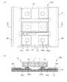
次に、図3を参照して、前記した発光装置10を、実装基板に実装した状態である実装基板付きの発光装置について説明する。
図3に示すように、実装基板付きの発光装置100は、実装基板9に複数の発光装置10が実装されたものである。なお、実装基板9に実装される発光装置10の個数は特に限定されるものではなく、1個以上が実装されていればよい。また、実装される発光装置は、図2(a)に示した発光装置10に限定されるものではなく、発光装置10に代えて、図2(b)に示した発光装置10A、図2(c)に示した発光装置10B、図2(d)に示した発光装置10C、図2(e)に示した発光装置10D、図2(f)に示した発光装置10E、又は図2(g)に示した発光装置10Fを用いることもできる。Next, with reference to FIG. 3, a light-emitting device with a mounting substrate in which the above-described light-emitting
As shown in FIG. 3, a
図3(a)に示した例は、3個の発光装置10を実装する領域を抜粋して模式的に示したものである。また、発光装置10は、3個の実装領域94の内の中央の1個の実装領域94に発光装置10を実装した様子を示している。 The example shown in FIG. 3A schematically shows an extracted area where three light emitting
図3(a)に示すように、実装基板9は、絶縁性の支持基板91上に、平面視で櫛状の負極側配線電極92n及び正極側配線電極92pが、櫛の歯に相当する箇所が互いに対向するように設けられている。負極側配線電極92n及び正極側配線電極92pの、一対の櫛の歯に相当する箇所を含む領域が、1個の発光装置10を実装するための実装領域94である。 As shown in FIG. 3A, the mounting
各実装領域94の、発光装置10のn側電極4n及びp側電極4pと接続する箇所には、負極用接続層93n及び正極用接続層93pとして、半田層が設けられている。負極用接続層93n及び正極用接続層93pは、リフロー工法等により溶融され、n側電極4nと負極側配線電極92nと、及び、p側電極4pと正極側配線電極92pとが、それぞれ接合される。
なお、負極側配線電極92n及び正極側配線電極92pは、それぞれ不図示の給電端子と接続されており、当該給電端子を介して外部電源から電力が供給されるように構成されている。A solder layer is provided as a negative
The negative
また、実装基板9の実装領域94を除く左右の上面領域は、絶縁性の反射層95によって被覆されている。図3に示した例では、反射層95は実装領域94の左右側のみ被覆しているが、更に、負極用接続層93n及び正極用接続層93pが設けられた領域以外を被覆するようにしてもよい。 The left and right upper surface regions of the mounting
反射層95は、発光素子1が発光する波長の光及び蛍光体層7が発光する波長の光に対して良好な反射性を有する反射膜である。反射層95としては、前記した反射性樹脂層11と同様の材料を用いることができ、粒状の光反射部材を含有した樹脂を塗布することで形成することができる。 The
また、本発明の実装基板付きの発光装置100は、発光装置10の全体を、透光性の封止部材で封止するようにしてもよい。封止部材としては、前記した蛍光体層7や反射層95に用いる樹脂材料、又は、ガラスやシリカゲルなどの無機材料を用いることができる。また、封止部材に、光拡散部材を添加するようにしてもよい。これによって、発光素子1が発光した光と、蛍光体層7が発光した光とを、良好に混色させることができる。光拡散部材としては、反射層95の光反射部材として例示したものと同様の部材を用いることができる。 Further, in the
また、本発明の発光装置10は、青色光と黄色光との組み合わせに限定されるものではなく、発光素子1が発光した波長の光の少なくとも一部を、蛍光体層7が波長変換して出力するものであればよい。例えば、発光素子1が青色光を発光し、蛍光体層7が赤色光及び/又は緑色光に変換するものや、発光素子1が紫外光を発光し、蛍光体層7がこれより長波長の青色光、緑色光、黄色光、赤色光などに変換するものも含まれる。 In addition, the
また、本発明の発光装置10は、フェイスダウン実装型に限定されるものではなく、フェイスアップ実装型やバーティカル実装型であってもよい。フェイスアップ実装型とする場合は、発光装置10を、例えば、以下のように構成することができる。まず、発光素子1の上面側となる半導体積層体3が設けられた面側を被覆するように、蛍光体層7を設けるようにする。また、発光素子1の全面電極5a及びカバー電極5bに代えて、ITO(インジウム・スズ酸化物)などの透光性を有する導電性材料を用いてp型半導体層3p上に全面電極を形成し、成長基板2の裏面側に反射層を設けるようにする。更に、蛍光体層7において、n側電極4n及びp側電極4pの表面が露出するように開口部を形成する。
そして、例えば、ワイヤを用いて、当該開口部に露出するn側電極4n及びp側電極4pと、実装基板9の負極側配線電極92n及び正極側配線電極92pとをそれぞれ電気的に接続するようにすればよい。The
Then, for example, using wires, the n-
また、フェイスアップ実装型又はバーティカル実装型の場合において、光取り出し面側に設けられた電極部を露出させた構造を形成するために、次のようにすることができる。まず、電極部の露出させる領域に、水溶性レジストで保護膜を形成し、スプレー塗布により蛍光体層7を形成する。その後、水溶性レジストを水洗することで、水溶性レジスト上に形成された蛍光体層7とともに剥離して、電極部を露出させることができる。
また、電極部上を含めて、スプレー塗布により蛍光体層7を形成した後、電極部上の蛍光体層7を、レーザーアブレーションなどにより除去することで、電極部を露出させることもできる。Further, in the case of the face-up mounting type or the vertical mounting type, in order to form a structure in which the electrode portion provided on the light extraction surface side is exposed, the following can be performed. First, a protective film is formed with a water-soluble resist in a region where the electrode part is exposed, and the
In addition, after the
[発光装置の動作]
次に、図3を参照(適宜図1参照)して、実装基板付きの発光装置100の動作について説明する。なお、説明の便宜上、発光素子1は青色光を発光し、蛍光体層7は黄色光を発光するものとして説明する。[Operation of light emitting device]
Next, the operation of the
図3に示した実装基板付きの発光装置100は、実装基板9に設けられた不図示の給電端子に外部電源が接続されると、正極側配線電極92p及び負極側配線電極92nを介して、発光装置10のp側電極4p及びn側電極4n間に電流を供給する。
p側電極4p及びn側電極4n間に電流が供給されると、発光素子1の発光層3aが青色光を発光する。In the
When a current is supplied between the p-
発光素子1の発光層3aが発光した青色光は、半導体積層体3及び成長基板2内を伝播して、発光素子1の上面又は側面から出射して、一部は蛍光体層7が含有する蛍光体粒子に吸収され、黄色光に変換されて外部に取り出される。また、青色光の一部は、蛍光体に吸収されずに蛍光体層7を透過して外部に取り出される。
なお、発光素子1内を下方向に伝播する光は、全面電極5aによって上方向に反射され、発光素子1の上面又は側面から出射する。
そして、発光装置10の外部に取り出された黄色光及び青色光が混色することにより、白色光が生成される。
なお、発光装置10の側面から下方向に取り出された光は、反射層95によって上方向に反射され、発光装置100から出射される。The blue light emitted from the light emitting layer 3a of the
The light propagating downward in the
The yellow light and the blue light extracted outside the
Note that light extracted downward from the side surface of the
次に、発光装置10に代えて、図2(b)に示した発光装置10Aを用いた実装基板付きの発光装置100を構成した場合について説明する。
前記したように、発光装置10Aは、発光素子1の側面の下部が蛍光体層7Aから露出している。このため、発光素子1の発光層3aが発光した青色光の一部は、発光素子1の側面の下部から出射して、青色光のまま発光装置10Aの外部に取り出される。発光素子1の側面の下部から取り出された青色光は、他の面から外部に取り出された黄色光及び青色光と混色され、全体として白色光として発光装置100から出射される。Next, a case where the
As described above, in the
発光素子1が発光する青色光の一部について、発光素子1の側面の下部から蛍光体層7Aを介さずに外部に取り出すようにすることで、生成される白色光において青色光の成分を十分に確保することができる。また、光取り出し効率のよい発光装置10Aとすることができる。 A part of blue light emitted from the
次に、発光装置10に代えて、図2(c)に示した発光装置10Bを用いた実装基板付きの発光装置100を構成した場合について説明する。
前記したように、発光装置10Bは、発光素子1の側面が蛍光体層7Bによって被覆されておらず、露出している。このため、発光素子1の発光層3aが発光した青色光の内で、横方向に伝播する光は、発光素子1の側面から出射して、青色光のまま発光装置10Bの外部に取り出される。発光素子1の側面から取り出された青色光は、上面から外部に取り出された黄色光及び青色光と混色され、全体として白色光として発光装置100から出射される。Next, a case where the
As described above, in the
発光素子1が発光する青色光の一部について、発光素子1の側面から、蛍光体層7Bを介さずに外部に取り出すようにすることで、生成される白色光において青色光の成分を十分に確保することができる。また、光取り出し効率のよい発光装置10Aとすることができる。 A part of the blue light emitted from the light-emitting
次に、発光装置10に代えて、図2(d)に示した発光装置10C、図2(e)に示した発光装置10D、図2(f)に示した発光装置10E、又は図2(g)に示した発光装置10Fを用いた実装基板付きの発光装置100を構成した場合について説明する。
前記したように、発光装置10C,10D,10E,10Fは、発光素子1の側面及び下面において、蛍光体層7で被覆されていない箇所は、反射性樹脂層11で被覆されている。このため、発光装置10,10A,10Bで漏らしていた青色光は、反射性樹脂層11で反射され、蛍光体層7を介して外部に取り出される。すなわち、発光素子1が発光した青色光が外部に取り出される際には、すべて蛍光体層7を介して取り出される。従って、発光装置10C,10D,10E,10Fを用いて構成した発光装置100は、良好な配光色度を得ることができる。Next, in place of the
As described above, in the
[発光装置の製造方法]
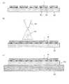
次に、図4を参照して、図3に示した発光装置100の製造方法について説明する。
図4に示すように、発光装置100の製造方法は、発光素子準備工程S11と、発光素子選別工程S12と、発光素子配列工程S13と、樹脂層形成工程S14と、仮硬化工程S15と、樹脂層分離工程S16と、本硬化工程S17と、実装工程S18と、を含み、この順で各工程が行われる。
以下、図5及び図6を参照(適宜図1、図3及び図4参照)して、各工程について詳細に説明する。[Method for Manufacturing Light Emitting Device]
Next, with reference to FIG. 4, the manufacturing method of the light-emitting
As shown in FIG. 4, the manufacturing method of the
Hereinafter, each step will be described in detail with reference to FIGS. 5 and 6 (refer to FIGS. 1, 3 and 4 as appropriate).
発光素子準備工程S11は、図1に示した構成の個片化された発光素子1を準備する工程である。
具体的には、まず、サファイアなどからなる成長基板2上(図1において下面)に、前記した半導体材料を用いて、n型半導体層3n、発光層3a及びp型半導体層3pを順次積層した半導体積層体3を形成する。The light emitting element preparation step S11 is a step of preparing the individual
Specifically, first, an n-type semiconductor layer 3n, a light-emitting layer 3a, and a p-type semiconductor layer 3p are sequentially stacked on the growth substrate 2 (lower surface in FIG. 1) made of sapphire or the like using the semiconductor material described above. The semiconductor stacked
半導体積層体3が形成されると、半導体積層体3の表面(図1において下面)の一部の領域について、p型半導体層3p、発光層3a及びn型半導体層3nの一部をエッチングにより除去してn型半導体層3nが底面に露出した段差部3bを形成する。
次に、段差部3bの底面にパッド電極であるn側電極4nを形成する。また、p型半導体層3p及び発光層3aを有する発光領域となる領域には、p型半導体層3pの下面の略全面を覆う反射性を有する全面電極5a及び全面電極5aの表面を被覆するカバー電極5bと、カバー電極5bの下面の一部にパッド電極であるp側電極4pを形成する。
更に、n側電極4n及びp側電極4pを除くウエハの表面全体に、例えば、スパッタリングにより、絶縁性のSiO2などの保護層6を形成する。When the semiconductor stacked
Next, an n-
Further, a protective layer 6 such as insulating SiO2 is formed on the entire surface of the wafer excluding the n-
以上により、ウエハ状態の発光素子1が形成される。
次に、ダイシング法、スクライブ法などにより、ウエハ状態の発光素子1を所定の分割領域で割断することにより個片化された発光素子1を作製することができる。
なお、ウエハを割断する前に、成長基板2の裏面を研磨して薄肉化するようにしてもよい。これにより、容易に割断することができる。Thus, the
Next, the
Note that before the wafer is cleaved, the back surface of the
次に、発光素子選別工程S12において、発光素子準備工程S11で作製した発光素子1から所定範囲の発光特性を有するものを選別する。ここで、所定範囲の発光特性とは、発光素子1が発光する光の中心波長及び/又は発光強度である。発光特性が揃った発光素子1を選別することにより、後記する樹脂層形成工程S14以降の工程により高い均一性で蛍光体層7を形成することと併せて、製造される発光装置10の装置間の色調のばらつきを抑制することができる。 Next, in the light emitting element selection step S12, those having the light emission characteristics within a predetermined range are selected from the
次に、発光素子配列工程S13において、図5(a)に示すように、延伸性を有するとともに、表面に粘着性を有するエキスパンドシート20上に、発光素子選別工程S12で選別した発光素子1を、側面が露出するように互いに離間して配列する。このとき、発光素子1のn側電極4n及びp側電極4pが設けられた面がエキスパンドシート20に対向するように載置する。
エキスパンドシートとしては、塩化ビニルなどの樹脂からなる半導体ウエハのダイシング用のシートを用いることができ、例えば、日東電工社製のダイシングテープV−8−Sを挙げることができる。Next, in the light emitting element arranging step S13, as shown in FIG. 5A, the
As the expanded sheet, a sheet for dicing a semiconductor wafer made of a resin such as vinyl chloride can be used. For example, a dicing tape V-8-S manufactured by Nitto Denko Corporation can be used.
また、発光素子1を載置する面に、粘着剤としてUV(紫外線)硬化型の樹脂を設けたエキスパンドシート20を用いるようにしてもよい。後記する実装工程S18において、エキスパンドシート20にUV光を照射して粘着性の樹脂を硬化させることにより、粘着性を消失させることができる。これによって、例えば、コレット50及びピン51(図6(c)参照)を用いて、エキスパンドシート20から、蛍光体層7が設けられた発光素子1、すなわち発光装置10を容易に剥離することができる。 Moreover, you may make it use the expand sheet |
次に、樹脂層形成工程S14において、図5(b)に示すように、発光素子1が配列して載置されたエキスパンドシート20上に、スプレー装置30によって、蛍光体層7の原料であるスラリーのスプレーSPを噴射することにより塗布し、樹脂層8を形成する。
ここで、発光素子1は、1次元に配列されていてもよく、2次元に配列されていてもよい。何れの配列の場合でも、発光素子1同士は、側面が露出するように互いに離間して配列されている。また、エキスパンドシート20は、不図示の載置台上に載置され、当該載置台とスプレー装置30とが、少なくとも水平方向に相対的に移動可能に構成されている。そして、スプレー塗布により、発光素子1の表面である上面及び側面と、エキスパンドシート20上とに、所定の厚さで一様に、かつ連続した樹脂層8が形成される。Next, in the resin layer forming step S <b> 14, as shown in FIG. 5B, the material for the
Here, the
スプレー装置30としては、特に限定されるものではないが、パルス状に、すなわち間欠的にスプレーSPを噴射するパルススプレー方式を用いることが好ましい。間欠的にスプレー噴射することにより、単位時間当たりの噴射量を少なくすることができる。このため、スプレー装置30を、少ない噴射量でスプレー噴射させながら低速で移動させることにより、凹凸形状を有する塗布面の側面や角部にも均一に塗布することができる。また、パルススプレー方式では、連続スプレー方式に比べて、ノズルからのスラリーの噴出速度を低減することなく、エアの風速を低減することができる。このため、パルススプレー方式では、連続スプレー方式と同様に塗布面に良好にスラリーを供給することができ、かつ、塗布されたスラリーがエア流によって乱されない。その結果、蛍光体の粒子と発光素子1の表面との密着性が高い塗布膜を形成することができる。 Although it does not specifically limit as the
また、パルススプレー方式では、噴射量を少なくすることができるため、1回のスプレー塗布による塗布量を低減して薄膜を形成することができる。そして、スプレー塗布を複数回繰り返すことにより、塗布膜である樹脂層8の膜厚を精度よく形成することができる。また、複数回のスプレー塗布の間に、1回ごと又は所定回数(例えば、3回)ごとに熱硬化性樹脂の仮硬化処理を行うことにより、側面部においても液垂れすることなく、均一性の高い良好な膜厚精度で樹脂層8を形成することができる。
なお、パルススプレー方式及び仮硬化処理の詳細については、後記する。Further, in the pulse spray method, since the spray amount can be reduced, a thin film can be formed by reducing the application amount by one spray application. And the film thickness of the
Details of the pulse spray method and the temporary curing process will be described later.
また、スプレー装置30によって塗布されるスラリーは、溶剤と、熱硬化性樹脂と、粒状の蛍光体とが含有される。スラリーに、更に無機フィラーを添加してもよい。また、このスラリーは、スプレー噴射可能で、発光素子1の側面部に塗布されたスラリーが液垂れしないように、適宜な粘度に調整される。 The slurry applied by the
熱硬化性樹脂としては、発光素子1が発光する波長の光及び蛍光体層7に含有される蛍光体が発光する波長の光に対して良好な透光性を有するものであれば特に限定されず、前記したシリコーン樹脂、エポキシ樹脂、ユリア樹脂などを用いることができる。具体的には、信越化学工業社製のシリコーン樹脂である製品名:LPS−3541を挙げることができる。
また、溶剤としては、n−ヘキサン、n−ヘプタン、トルエン、アセトン、イソプロピルアルコールなどの有機溶剤を用いることができる。The thermosetting resin is not particularly limited as long as it has good translucency with respect to light having a wavelength emitted from the
Moreover, as a solvent, organic solvents, such as n-hexane, n-heptane, toluene, acetone, isopropyl alcohol, can be used.
また、熱硬化性樹脂は、常温で固体のものを溶剤に溶解させて用いることが好ましい。これによって、塗布されたスラリーである樹脂層8を、仮硬化処理によって適宜な硬度に硬化させることができる。 Moreover, it is preferable to use the thermosetting resin by dissolving a solid at room temperature in a solvent. Thereby, the
ここで、仮硬化とは、熱硬化性樹脂が完全に架橋反応を起こす硬化温度よりも低い所定温度で所定時間加熱することで、樹脂層8に含有される溶剤を蒸発させ、樹脂層8を不完全に硬化させることをいうものである。すなわち、仮硬化処理における加熱温度及び加熱時間を制御することにより溶剤の蒸発量を制御することができ、その結果として、樹脂層8の硬度を調整することができる。
また、本硬化とは、熱硬化性樹脂が架橋反応する温度以上(硬化温度以上)の所定温度で、所定時間加熱することにより、熱硬化性樹脂が架橋反応により硬化させることをいうものである。また、本硬化処理を行うことにより、樹脂層8に含有される溶剤は略完全に蒸発する。Here, the temporary curing means that the solvent contained in the
The main curing means that the thermosetting resin is cured by a crosslinking reaction by heating for a predetermined time at a predetermined temperature that is equal to or higher than a temperature at which the thermosetting resin undergoes a cross-linking reaction (curing temperature or higher). . Further, by performing the main curing process, the solvent contained in the
以下に、スラリーの処方例を挙げる。
熱硬化性樹脂:シリコーン樹脂(LPS3541)
溶剤:n−ヘプタン
蛍光体:熱硬化性樹脂:溶剤(質量比)=15:10:15Examples of slurry formulations are given below.
Thermosetting resin: Silicone resin (LPS3541)
Solvent: n-heptane Phosphor: Thermosetting resin: Solvent (mass ratio) = 15: 10: 15
また、スラリーは、粘度が、0.01〜1000mPa・s(ミリパスカル秒)、より好ましくは0.1〜100mPa・sとなるように成分を調整することが好ましい。スラリーをこの範囲の粘度とすることにより、均一なスプレー塗布を可能とするとともに、塗布後の過剰な液垂れを防止することができる。 Further, it is preferable to adjust the components so that the slurry has a viscosity of 0.01 to 1000 mPa · s (millipascal second), more preferably 0.1 to 100 mPa · s. By setting the slurry to a viscosity in this range, uniform spray coating can be achieved and excessive dripping after coating can be prevented.
また、パルススプレー方式による塗布法では、蛍光体、樹脂及び溶剤を混合した、蛍光体濃度が希薄なスラリーを、気体と液体とを同時に噴霧可能な2流体ノズルを用いて、それぞれパルス状にON/OFF駆動して、ワーク(被塗布体)に塗布する。このとき、ワークを昇温しておくことで、ワーク表面で溶剤は瞬時に蒸発して極めて薄い蛍光体を含有した樹脂塗膜を形成することができる。すなわち、実質的に塗布と仮硬化とを同時に行うものである。
これを繰り返すことで、蛍光体を含有する樹脂の薄膜を積層した樹脂層8を形成することができる。Also, in the application method by the pulse spray method, each slurry is turned on in the form of a pulse by using a two-fluid nozzle capable of simultaneously spraying a gas and a liquid with a mixture of phosphor, resin and solvent and having a thin phosphor concentration. / OFF drive to apply to workpiece (object). At this time, by raising the temperature of the workpiece, the solvent instantly evaporates on the surface of the workpiece and a resin coating film containing an extremely thin phosphor can be formed. That is, the application and the temporary curing are substantially simultaneously performed.
By repeating this, the
また、パルススプレー方式を用いることで、エキスパンドシート20の延伸による個片化に最適な特徴を有する樹脂層8を形成することができる。すなわち、蛍光体と樹脂との配合において蛍光体の比率が高く、かつ、総膜厚が薄い樹脂層8を形成することができる。 Further, by using the pulse spray method, the
ここで、蛍光体比率=(蛍光体質量)/(蛍光体質量+樹脂質量)は、好ましくは30〜99質量%、より好ましくは50〜90質量%、更に好ましくは60〜85質量%である。
蛍光体比率が、好ましくは30質量%以上、より好ましくは50質量%以上、更に好ましくは60質量%以上となるように、樹脂に対する蛍光体の含有量を多くすることで、エキスパンドシート20の延伸時に、樹脂層8に亀裂が入り易くなり、発光素子1の側面の下部での樹脂層8の引き千切りによる切断が容易となる。
また、蛍光体比率が、好ましくは99質量%以下、より好ましくは90質量%以下、更に好ましくは85質量%以下となるように樹脂を含有させることにより、蛍光体粒子同士及び樹脂層8と発光素子1とを十分な強度で接着させることができる。Here, the phosphor ratio = (phosphor mass) / (phosphor mass + resin mass) is preferably 30 to 99% by mass, more preferably 50 to 90% by mass, and still more preferably 60 to 85% by mass. .
The expanded
In addition, phosphor is contained between the phosphor particles and the
また、蛍光体に加えて無機材料からなるフィラーを添加してもよく、蛍光体及びフィラーからなる無機材料粒子の固体分が多いほどエキスパンドシート20の延伸による樹脂層8の引き千切りによる切断が容易となる。
この場合は、無機材料比率=(蛍光体質量+無機フィラー質量)/(蛍光体質量+無機フィラー質量+樹脂質量)が、好ましくは30〜99質量%、より好ましくは50〜90質量%、更に好ましくは60〜85質量%とする。Further, a filler made of an inorganic material may be added in addition to the phosphor, and the more the solid content of the inorganic material particles made of the phosphor and the filler is, the easier it is to cut the
In this case, the ratio of inorganic material = (phosphor mass + inorganic filler mass) / (phosphor mass + inorganic filler mass + resin mass) is preferably 30 to 99% by mass, more preferably 50 to 90% by mass, and further Preferably it is 60-85 mass%.
更にまた、樹脂層8を、複数の薄膜を積層して形成する場合は、複数層積層した薄膜毎に無機材料比率が異なっていてもよい。またこのとき、樹脂層8を構成する複数の薄膜の内、少なくとも1層において、前記した無機材料比率とすることが好ましい。この場合は、当該1層は、無機材料比率が50質量%以上とすることが好ましい。これによって、他の薄膜の無機材料比率が低い場合でも、エキスパンドシート20を延伸させたときに、当該1層の薄膜を起点として亀裂が生じ、樹脂層8の引き千切りを容易に行うことができる。 Furthermore, when the
また、樹脂層8を、複数の薄膜を積層して形成する場合において、各薄膜は、膜内で無機材料(蛍光体及び無機フィラー)が、下部に沈降した状態で形成されることが好ましい。すなわち、樹脂層8が、無機材料比率の高い無機材料リッチ層と無機材料比率の低いクリア層とが交互に積層された形状であることが好ましい。このように構成することで、微視的に無機材料比率が高い部位が形成されるため、エキスパンドシート20を延伸させた際に、当該無機材料比率が高い部位に亀裂が生じやすくなる。従って、樹脂層8の切断を、より容易に行うことができる。
このような構造は、各薄膜についてスラリーをスプレー塗布した際に、スラリーに含有されている無機材料が当該薄膜の下部に沈降する時間を考慮して、スラリーにおける溶剤比率や仮硬化温度などを調整することで形成することができる。Moreover, when forming the
In such a structure, when the slurry is spray-coated on each thin film, the solvent ratio in the slurry and the temporary curing temperature are adjusted in consideration of the time for the inorganic material contained in the slurry to settle to the lower part of the thin film. By doing so, it can be formed.
また、塗布膜である樹脂層8の総膜厚(最大厚さ箇所)は、好ましくは1〜500μm、より好ましくは5〜200μm、更に好ましくは10〜100μmである。このように、樹脂層8の厚さを薄くすることで、エキスパンドシート20の延伸による樹脂層8の引き千切りによる切断が容易となる。
更に、引き千切りにより切断される箇所(発光素子1の側面下端部における樹脂層8の分離箇所)における樹脂層8の膜厚は、200μm以下とすることが好ましく、かつ、発光素子1の表面に形成される樹脂層8よりも薄く形成されることが好ましい。これにより、切断箇所を特定でき、位置精度よく切断することができる。
また、積層後の樹脂層8における蛍光体の含有量は、単位面積当たりの質量で、0.1〜50mg/cm2となるように調整することが好ましい。蛍光体の含有量をこの範囲にすることにより、色変換を十分に行うことができる。Moreover, the total film thickness (maximum thickness location) of the
Furthermore, the film thickness of the
Moreover, it is preferable to adjust so that content of the fluorescent substance in the
パルススプレー方式による塗布法の他の利点は、樹脂の硬化条件を制御することで樹脂層8の立体的な構造を制御できることである。立体的な構造を制御することで、エキスパンドシート20の延伸による樹脂層8の発光素子1からの引き剥しや樹脂層8の切断位置を制御することができる。
更にスプレー塗布時に、適宜な形状の開口を有するマスクを使用して塗布領域ごとに塗布量を制御することで、より繊細な立体構造を形成することが可能となる。例えば、発光素子1の外縁部(境界)近傍のエキスパンドシート20上を覆うマスクを用いてスプレー塗布することで、発光素子1の上面及び側面に形成される樹脂層8に比べて、当該発光素子1の外縁部近傍のエキスパンドシート20上に形成される樹脂層8の膜厚を薄くすることができる。Another advantage of the application method by the pulse spray method is that the three-dimensional structure of the
Furthermore, a finer three-dimensional structure can be formed by controlling the coating amount for each coating region using a mask having an appropriately shaped opening during spray coating. For example, compared to the
ここで、図7を参照して、スプレー装置30の例について説明する。
図7に示すスプレー装置30は、塗布液として固形粒子を含有するスラリーの塗布に適した装置である。すなわち、塗布液であるスラリーを常時撹拌することでスラリーに含有される固形粒子を沈降させることなく、スラリー中に常に一様に分散させ、固形粒子が一様に分散されたスラリーをスプレー噴射するように構成されている。
このために、図7に示すスプレー装置30は、2本のシリンジ31,32と、シリンジ31,32の下端部を接続する流通路33と、流通路33の中ほどに設けられたノズル付きバルブ34とを備えて構成されている。Here, an example of the
The
For this purpose, the
シリンジ31は、内部にプランジャ31aを備え、スラリーSLを収容する円筒形の容器である。シリンジ31の下端部は狭窄しており、当該下端部は流通路33と連通している。また、シリンジ31の上端部からは、不図示のバルブを介して内部に圧縮空気31bが導入される。そして、シリンジ31内のスラリーSLは、導入された圧縮空気31bによって、プランジャ31aを介して加圧される。 The
シリンジ32は、シリンジ31と同じ構成をしており、内部に収容されるスラリーSLは、狭窄した下端部が流通路33と連通している。従って、シリンジ31とシリンジ32とは、流通路33を介して連通しており、それぞれの内部に収容されるスラリーSLは混ざり合うことができるようになっている。
また、シリンジ32の上端部からは、シリンジ31と同様に、不図示のバルブを介して内部に圧縮空気32bが導入される。そして、シリンジ32内のスラリーSLは、導入された圧縮空気32bによって、プランジャ32aを介して加圧される。The
Moreover, from the upper end part of the
また、ノズル付きバルブ34は、流通路33の中ほどに設けられ、流通路33内を流通するスラリーSLを下方向に開口するノズルから吐出可能に構成されている。また、ノズル付きバルブ34には、外部から圧縮空気が導入され、ノズルから噴射することで、スラリーSLをスプレーSPとして噴射させることができるように構成されている。また、ノズル付きバルブ34は、ノズルから吐出させるスラリー量及び圧縮空気量を、それぞれに対応したバルブの開度を調整することにより制御できるように構成されている。 Further, the nozzle-equipped
次に、スプレー装置30において、スラリーSLを撹拌する動作について説明する。
シリンジ31及びシリンジ32の各上端部からは、それぞれ異なる圧縮空気源から圧縮空気が供給される。そして、シリンジ31に導入される圧縮空気31bの圧力と、シリンジ32に導入される圧縮空気32bの圧力とが、異なる位相(例えば、逆位相)で脈動するように圧縮空気が供給される。これによって、スプレー装置30は、シリンジ31,32内のスラリーSLを、流通路33を介して互いに往復させることができ、その結果として、当該スラリーSLを撹拌することができる。Next, the operation | movement which stirs slurry SL in the
From each upper end part of the
このようにしてスラリーSLを常時撹拌することにより、流通路33内には、固形粒子である蛍光体が常に均一に分散されたスラリーSLが流通する。そして、ノズル付きバルブ34によって流通路33内を流通するスラリーSLを吐出させることにより、蛍光体粒子が均一に含有されるスプレーSPを噴射することができる。 By constantly stirring the slurry SL in this manner, the slurry SL in which the phosphors that are solid particles are always uniformly distributed flows in the
次に、スプレー装置30を用いたパルススプレー方式のスプレー塗布について説明する。
パルススプレー方式とは、前記したように、スプレーSPをパルス状に、すなわち間欠的に噴射する方式である。スプレー装置30において、ノズル付きバルブ34の、バルブ開度を調整することにより、スプレーSPの噴射量を制御することができる。簡単には、バルブの開度を「開」と「閉」との2段階とし、開閉を所定の周期及びデューティ比で制御することによりパルススプレーを行うことができる。
バルブ開閉のタイミングは、スラリーSLと圧縮空気とについて同じとしてもよいし、圧縮空気の方が長く開状態となるようにしてもよい。
また、単位時間当たりのスプレーSPの噴射量を精度よく維持するためには、バルブ開閉の周期は30〜3600回/分程度とすることが好ましい。Next, pulse spraying spray application using the
As described above, the pulse spray method is a method of spraying the spray SP in a pulse shape, that is, intermittently. In the
The timing for opening and closing the valve may be the same for the slurry SL and the compressed air, or the compressed air may be opened longer.
In order to maintain the spray amount of the spray SP per unit time with high accuracy, the valve opening / closing cycle is preferably about 30 to 3600 times / minute.
なお、パルススプレー方式及びスラリーの塗布に適したスプレー装置については、例えば、参考文献1及び参考文献2に詳細に説明されているため、更なる説明は省略する。
(参考文献1)特開昭61−161175号公報
(参考文献2)特開2003−300000号公報In addition, since the spray apparatus suitable for the pulse spray method and slurry application is described in detail in
(Reference 1) JP 61-161175 (Reference 2) JP 2003-300000
図5に戻って(適宜図1、図3及び図4参照)、製造工程についての説明を続ける。
次に、仮硬化工程S15において、図5(c)に示すように、加熱装置40を用いて、樹脂層形成工程S14で形成された樹脂層8を仮硬化させる。これによって、樹脂層8は、粘液状態から適宜な硬度と引張強度とを有する状態に変化する。
なお、加熱装置40の加熱方式は特に限定されず、図5(c)に示すように、エキスパンドシート20の下面に接触させるヒータを用いたものや、赤外線を照射するものなど、適宜な方式のヒータやオーブンなどを用いることができる。Returning to FIG. 5 (see FIGS. 1, 3 and 4 as appropriate), the description of the manufacturing process will be continued.
Next, in temporary hardening process S15, as shown in FIG.5 (c), using the
The heating method of the
本発明では、熱硬化性樹脂の種類や含有量に応じて、加熱装置40による加熱時間又は/及び加熱温度を調整することにより、この仮硬化の程度を調整することができる。
また、前記したようにスプレー塗布を複数回に分けて行う場合は、樹脂層形成工程S14と仮硬化工程S15とを交互に複数回繰り返し行うようにしてもよい。この場合、スプレー塗布の回数と仮硬化処理の回数とは同じである必要はなく、例えば、スプレー塗布を3回行うごとに、1回の仮硬化処理を行うようにしてもよい。
このように、複数回のスプレー塗布を行う途中で適宜に仮硬化処理を行うことにより、特に発光素子1の側面において、塗布したスラリーの液垂れを防止して、均一で膜厚の厚い樹脂層8を形成することが可能となる。In the present invention, the degree of this temporary curing can be adjusted by adjusting the heating time or / and the heating temperature by the
Moreover, as described above, when spray coating is performed in a plurality of times, the resin layer forming step S14 and the temporary curing step S15 may be alternately repeated a plurality of times. In this case, the number of spray coatings and the number of temporary curing processes do not have to be the same. For example, every time spray coating is performed three times, one temporary curing process may be performed.
In this way, by performing a temporary curing process appropriately during the spray application of a plurality of times, it is possible to prevent dripping of the applied slurry, particularly on the side surface of the light-emitting
更にまた、スプレー塗布の後に、加熱装置40を用いた積極的な加熱処理をする仮硬化工程S15を行わず、次工程である樹脂層分離工程S16を行うまでの間に、常温状態に置かれることによって硬化が進行する自然硬化のみが、なされるようにしてもよい。 Furthermore, after the spray coating, the temporary curing process S15 that performs the positive heat treatment using the
なお、前記した処方例のスラリーを用いる場合は、仮硬化処理を、例えば、以下のような条件で行うことができる。
(樹脂層形成工程)
樹脂層8として、1層当たりの塗布量が約0.7mg/cm2として、3層積層する。
(仮硬化工程)
仮硬化処理として、3層積層するごとに、オーブンを用いて150℃で5分間の加熱処理を行う。In addition, when using the slurry of an above-described prescription example, a temporary hardening process can be performed on the following conditions, for example.
(Resin layer forming process)
As the
(Temporary curing process)
As the temporary curing treatment, heat treatment is performed at 150 ° C. for 5 minutes every time three layers are laminated.
次に、樹脂層分離工程S16において、図6(a)に示すように、エキスパンドシート20を延伸(エキスパンド)させる。なお、エキスパンドシート20の延伸は、延伸方向についてのエキスパンドシート20の両端を適宜な治具を用いて把持し、当該治具を延伸方向に離れるように移動させることにより行うことができる。
ここで、発光素子1が1次元に配列されている場合は、当該配列方向にエキスパンドシート20を延伸させる。また、発光素子1が2次元に配列されている場合は、エキスパンドシート20を2つの配列方向に同時に延伸させてもよいし、1方向ずつ順次に延伸させるようにしてもよい。Next, in the resin layer separation step S <b> 16, as shown in FIG. 6A, the expanded
Here, when the
エキスパンドシート20を発光素子1の配列方向に、すなわち、シート面内の方向である横方向に延伸させることにより、発光素子1の上面に形成された樹脂層8である上面部樹脂層8a及び側面に形成された樹脂層8である側面部樹脂層8bが、エキスパンドシート20上に形成された樹脂層8であるシート部樹脂層8cから分離される。そして、発光素子1の表面に残った上面部樹脂層8a及び側面部樹脂層8bが、蛍光体層7(図1参照)となる。 The expanded
また、エキスパンドシート20を延伸させて樹脂層8を分離した後に、発光素子1の上面又は上面及び側面に形成された樹脂層8である蛍光体層7を、薄い透光性の樹脂層で保護膜として被覆するようにしてもよい。また、透光性の樹脂層を設けることで、光取り出し性を向上させることができる。
この透光性の樹脂層は、蛍光体及び無機フィラーを含有せず、樹脂層8の形成に用いた熱硬化性樹脂を含有する溶液をパルススプレー法で塗布し、その後に加熱することで硬化させて形成することができる。Further, after the expanded
This translucent resin layer does not contain a phosphor and an inorganic filler, and is cured by applying a solution containing the thermosetting resin used for forming the
なお、蛍光体層7となる樹脂層8を分離した後に、透光性の樹脂層を形成するようにすることで、樹脂層8の分離(切断)の際の負荷が増加しない。また、透光性の樹脂層は、蛍光体層7と比較して十分に薄く形成することで、蛍光体層7上からエキスパンドシート20上にまで連続して形成した場合でも、エキスパンドシート20の更なる延伸や、後記する実装工程S18におけるピックアップによって、蛍光体層7上の透光性の樹脂層を、エキスパンドシート20上の透光性の樹脂層から容易に分離することができる。 In addition, after separating the
また、樹脂層分離工程S16において、エキスパンドシート20を、横方向(シート面内の方向)に延伸させずに、又は横方向の延伸に加えて、縦方向(シート面に垂直な方向)に延伸させるようにしてもよい。
エキスパンドシート20の延伸方向と樹脂層8の分離との関係については後記する。In the resin layer separation step S16, the expanded
The relationship between the stretching direction of the expanded
本発明では、エキスパンドシート20を延伸させることにより、ダイシングなどの割断工法を用いることなく、簡便に蛍光体層7が形成された発光装置10を個片化することができる。また、発光素子1の側面に形成された蛍光体層7の厚さは、スプレー塗布による塗布膜の膜厚精度に依存し、個片化工程に依存しない。このため、スプレー塗布による成膜の膜厚精度で蛍光体層7を形成することができる。 In the present invention, by extending the expanded
次に、本硬化工程S17において、図6(b)に示すように、加熱装置40を用いて、樹脂層8を本硬化させる。
加熱装置40は、仮硬化工程S15で用いたものと同じものを用いることができるが、より短時間で本硬化処理を完了させるために、仮硬化処理に用いるものよりも加熱能力の高い加熱装置を用いるようにしてもよい。Next, in the main curing step S <b> 17, as shown in FIG. 6B, the
The
なお、前記した処方例のスラリーを用いる場合は、本硬化処理を、例えば、以下のような条件で行うことができる。但し、樹脂層形成工程S14及び仮硬化工程S15は、前記した条件(1層当たり約0.7mg/cm2で塗布し、3層積層するごとに、150℃で5分間加熱処理する)で行うものとする。
樹脂層8を、当該条件で合計9層積層して形成した場合、本硬化処理として、オーブンを用いて180℃で4時間加熱処理を行うようにすることができる。In addition, when using the slurry of an above-described prescription example, this hardening process can be performed on the following conditions, for example. However, the resin layer forming step S14 and the pre-curing step S15 are performed under the above-described conditions (applied at about 0.7 mg / cm2 per layer and heat-treated at 150 ° C. for 5 minutes each time three layers are laminated). Shall.
When the
次に、実装工程S18において、図6(c)に示すように、コレット50及びピン51を用いて、発光装置10を1個ずつピックアップし、図3に示したように、実装基板9の実装領域94に載置する。より詳細には、コレット50で発光装置10の上面に設けられた蛍光体層7を吸着するとともに、エキスパンドシート20の裏面側からピン51を用いて発光装置10の下面から押し上げる。これによって、発光装置10をエキスパンドシート20から容易に剥離することができる。 Next, in the mounting step S18, as shown in FIG. 6C, the
また、エキスパンドシート20が発光装置10を担持するための粘着剤として、UV硬化樹脂層を設けている場合は、コレット50及びピン51を用いた発光装置10のピックアップを始める前に、エキスパンドシート20にUV光を照射し、粘着剤を硬化させることにより粘着性を消失させる。これによって、発光装置10をエキスパンドシート20から、より容易に剥離することができる。 When the expanded
すべての実装領域94に発光装置10を載置した後、リフロー装置などを用いて加熱することで負極用接続層93n及び正極用接続層93pである半田層を溶融させ、各発光装置10のn側電極4nと負極側配線電極92nと、及び、p側電極4pと正極側配線電極92pとをそれぞれ電気的に接合する。これによって、発光装置10の実装基板9への実装が完了する。 After the
なお、フェイスダウン実装型の発光装置10の電極と実装基板9の電極との接合は、前記したように加熱による半田接合法を用いることが好ましい。圧力や超音波振動を利用した接合方式であるフリップチップ実装に比べて、発光装置10の上面に設けられた樹脂層である蛍光体層7に機械的な負荷が印加されないため、蛍光体層7に割れなどの損傷が発生するリスクを回避することができる。 Note that, as described above, it is preferable to use the solder bonding method by heating for bonding the electrodes of the face-down mounting type
また、各電極を接合した後で、発光装置10を、樹脂やガラスなどの封止部材を用いて封止するようにしてもよい。
以上の工程によって、実装基板付きの発光装置100が完成する。Moreover, after joining each electrode, you may make it seal the light-emitting
Through the above steps, the
次に、図8を参照して、エキスパンドシート20の延伸によって、発光素子1の表面に形成された樹脂層8が、シート部樹脂層8cから分離される様子について詳細に説明する。 Next, with reference to FIG. 8, a state where the
図8(a)に示した例は、仮硬化工程S15において、樹脂層8の仮硬化を自然硬化のみ、又は極弱くしか行わなかった場合を示すものである。この場合の樹脂層8は、粘性は側面部樹脂層8bが液垂れしない程度に高いが、引張強度は弱くて千切れやすい状態である。エキスパンドシート20をシート面内の方向である横方向に延伸することにより、シート部樹脂層8cは、エキスパンドシート20の延伸に伴って、薄く引き延ばされるが、側面部樹脂層8bは、発光素子1の側面との密着力により当該側面から剥離されず、シート部樹脂層8cとの接続部が引き延ばされる。そして、当該接続部に、図8(a)において樹脂層8中に記載した矢印で示したように引張力が作用して一定以上引き延ばされることにより、例えば、図8(a)において破線で示した分離線で、すなわち、発光素子1の側面の下端部で切断されることになる。
従って、図8(a)に示した例では、上面の全面及び側面の全面に蛍光体層7が形成された図2(a)に示した発光装置10が作製される。The example shown in FIG. 8A shows a case where the temporary curing of the
Therefore, in the example shown in FIG. 8A, the
なお、樹脂層8が実質的に未硬化の状態で、エキスパンドシート20を横方向に延伸させた場合、樹脂層8の粘性や膜厚によっては、側面部樹脂層8bとシート部樹脂層8cとが良好に分離できない場合がある。
そこで、樹脂層8が未硬化の状態で、所定の延伸率で1回目のエキスパンドシート20の延伸を行った後に、仮硬化を行い、その後に2回目のエキスパンドシート20の延伸を行うことで、樹脂層8を分離するようにしてもよい。When the expanded
Therefore, after the
具体的には、エキスパンドシート20の1回目の延伸により、図8(a)に示すように、シート部樹脂層8cが薄く延ばされた状態となる。そこで、樹脂層8を仮硬化させ、樹脂層8の粘度を上昇させる。このとき、側面部樹脂層8bとシート部樹脂層8cとでは膜厚が異なるため、両者の境界部に応力が集中し易い形状となっている。
そして、エキスパンドシート20の2回目の横方向の延伸を行うことにより、図8(a)に破線で示した分離線で、すなわち、発光素子1の側面の下端部で、樹脂層8が分離線で引き千切りにより切断され、シート部樹脂層8cを分離して除去することができる。
また、2回目のエキスパンドシート20の延伸は、横方向に限らず、図8(d)に示すように、縦方向に延伸させるものであってもよい。縦方向に延伸させた場合でも、図8(a)の分離線の近傍で、シート部樹脂層8cを切断することができる。Specifically, as illustrated in FIG. 8A, the sheet
And by extending | stretching the horizontal direction of the 2nd time of the expanded
Moreover, the expansion of the expanded
なお、2回目のエキスパンドシート20の延伸を行う際の樹脂層8は、例えば、無機材料比率が60質量%、シート部樹脂層8cの厚さが約60μm、側面部樹脂層8bの厚さが約10〜40μm、溶剤はほぼ揮発している状態とすることができる。この状態でエキスパンドシート20を延伸すると、樹脂層8を、発光素子1の側面の下端で切断することができる。また、この樹脂層8の完全硬化(本硬化)後の硬度は、デュロメータタイプAによる硬さで60〜80である。
また、シート部樹脂層8cの厚さは、薄いほど好ましいが、側面部樹脂層8bの厚さ及びその均一性を考慮して、1回目のエキスパンドシート20の延伸量やスラリーの粘度などを調整することができる。For example, the
Further, the thickness of the
また、本例においては、スプレー塗布する際に、塗布量を調整するためのマスクを使用することなく樹脂層8を形成している。本例では、樹脂層8をスプレー塗布により均一な厚さで形成した後で、エキスパンドシート20を延伸することにより、シート部樹脂層8cを薄膜化して、発光素子1の側面下端での切断に適した形状を得るようにしている。更に、無機材料比率を調整することにより、エキスパンドシート20の延伸による引き千切りによる切断が容易となるようにしている。 In this example, the
このように、所望の切断位置で樹脂層8を分離するために、蛍光体(及び無機フィラー)と樹脂の比率、蛍光体(及び無機フィラー)のサイズ・形状、樹脂の性質である硬度・密着性・強度・伸びなどを考慮して、仮硬化後の樹脂層8の状態を調整することができる。更に、樹脂層8の形状・膜厚や樹脂層8の切断箇所の膜厚が薄くなるように制御するために、エキスパンドシート20の延伸率や、マスクの使用、スラリー中の溶剤量、乾燥温度も適宜に調整することができる。
なお、図8(a)〜(d)に示した樹脂層8は、スプレー塗布した段階では、樹脂層8が発光素子1の上面からエキスパンドシート20上まで均一な厚さで塗布された場合を示すものである。Thus, in order to separate the
The
次に、図8(b)に示した例は、仮硬化工程S15において、樹脂層8の仮硬化を比較的弱く行った場合を示すものである。この場合の樹脂層8は、仮硬化されることにより、ある程度は剛性を有するとともに、引張力が作用すると延伸する物性を有する。側面部樹脂層8bはある程度の剛性を有するため、側面部樹脂層8bがエキスパンドシート20のシート面内の方向である横方向の延伸に伴って、図8(b)において樹脂層8中に記載した右下向きの矢印の方向に、シート部樹脂層8cから作用を受ける引張力の水平方向成分が、発光素子1の側面との密着力よりも大きくなると、発光素子1の側面から剥離される。更に側面部樹脂層8bとシート部樹脂層8cとの接続部が延伸し、一定以上引き延ばされると、図8(b)において破線で示した分離線で、すなわち、発光素子1の側面の上端と下端との間で、切断されることになる。
従って、図8(b)に示した例では、上面の全面及び側面の一部に蛍光体層7Aが形成された図2(b)に示した発光装置10Aが作製される。Next, the example shown in FIG. 8B shows a case where the temporary curing of the
Therefore, in the example shown in FIG. 8B, the
なお、図8(b)に示した例では、揮発性の有機溶剤の蒸発が十分でなくて樹脂層8内に残留しているとともに、樹脂の重合も進んでいない。すなわち、樹脂層8は、仮硬化が不十分な状態となっている。このため、この状態の樹脂層8の樹脂は脆く、強度が不十分であり、エキスパンドシート20の延伸による樹脂層8の切断は発光素子1の側面部で切断される。なお、この切断位置は、樹脂層8の膜厚やスラリーの処方、仮硬化の温度及び時間などの条件を調整すること制御することができる。 In the example shown in FIG. 8B, the volatile organic solvent is not sufficiently evaporated and remains in the
次に、図8(c)に示した例は、仮硬化工程S15において、樹脂層8の仮硬化を比較的強く行った場合を示すものである。この場合の樹脂層8は、仮硬化されることにより、十分な剛性を有するとともに、引張力が作用しても殆ど延伸しないという物性を有する。側面部樹脂層8bは十分な剛性を有するため、側面部樹脂層8bがエキスパンドシート20のシート面内の方向である横方向の延伸に伴ってシート部樹脂層8cから作用を受ける引張力が、発光素子1の側面との密着力よりも大きくなると、発光素子1の側面から剥離される。また、上面部樹脂層8aは、発光素子1の上面と密着しており、側面部樹脂層8bとの接続部に引張力が作用しても剥離されない。このため、当該接続部に一定以上の引張力が作用すると、最も応力が集中する樹脂層8の角部8dに亀裂が生じ、図8(c)に破線で示した分離線で、すなわち、発光素子1の側面の上端で樹脂層8が切断される。
従って、図8(c)に示した例では、上面の全面にのみ蛍光体層7Bが形成された図2(c)に示した発光装置10Bが作製される。Next, the example shown in FIG. 8C shows a case where the
Accordingly, in the example shown in FIG. 8C, the
図8(c)に示した例では、樹脂層8の仮硬化が十分に進んでいるため、樹脂強度が十分である。このため、エキスパンドシート20の延伸により水平方向(横方向)に力が加わると、発光素子1から樹脂層8を引き剥す力が作用し、発光素子1の上部で樹脂層8が切断される。なお、このときには、樹脂層8に含有される樹脂は理論的な硬度に達していると考えられる。 In the example shown in FIG. 8C, the
次に、図8(d)に示した例は、仮硬化工程S15において樹脂層8の仮硬化を行い、樹脂層分離工程S16においてエキスパンドシート20をシート面に垂直な方向である縦方向に延伸させる場合を示すものである。仮硬化の程度は特に限定されず、図8(a)に示した例(自然硬化のみ)、ないし、図8(c)に示した例(引張力によって殆ど延伸しない程度)における仮硬化とすることができる。以下の説明では、図8(c)に示した例と同程度に樹脂層8を比較的強く仮硬化したものとして説明する。 Next, in the example shown in FIG. 8D, the
本例において、エキスパンドシート20を縦方向に延伸させるとは、エキスパンドシート20の裏面側から、例えば、ピン51を用いて、エキスパンドシート20をシート面に垂直な方向に延伸させることをいうものである。エキスパンドシート20の縦方向の延伸に伴って、発光素子1が上方に持ち上げられ、発光素子1の表面に形成された樹脂層8も上方に持ち上げられることになる。これによって、側面部樹脂層8bには、上向きの引張力が作用する。一方、シート部樹脂層8cは、エキスパンドシート20の表面との密着力が大きいため、横方向の引張力が作用してもエキスパンドシート20から剥離されない。このため、側面部樹脂層8bとシート部樹脂層8cの接続部において最も応力が集中する角部8dに亀裂が生じ、図8(d)に破線で示した分離線で、すなわち、発光素子1の側面の下端で樹脂層8が切断される。
従って、図8(d)に示した例では、上面の全面及び側面の全面に蛍光体層7が形成された図2(a)に示した発光装置10が作製される。In this example, extending the expanded
Therefore, in the example shown in FIG. 8D, the
図8(d)に示した例では、垂直方向に力が加わるため、図8(c)に示した例と異なり、発光素子1の側面に形成された樹脂を剥がす力が作用しないため、仮硬化を十分行って樹脂の強度を高くしても、切断箇所は発光素子1の側面下部となる。 In the example shown in FIG. 8D, a force is applied in the vertical direction. Unlike the example shown in FIG. 8C, the force that peels off the resin formed on the side surface of the
なお、樹脂層8を比較的弱く仮硬化した場合、又は自然硬化のみとした場合は、エキスパンドシート20の縦方向の延伸により、側面部樹脂層8bに作用する縦方向の引張力により、側面部樹脂層8bとシート部樹脂層8cとの接続部が一定以上引き延ばされると、当該接続部の引張強度に応じて、接続部の何れかの箇所で切断されることになる。
従って、エキスパンドシート20を縦方向に延伸することにより、樹脂層8の仮硬化の程度に関らず、発光素子1の側面の下端で樹脂層8が切断されることになる。When the
Therefore, by extending the expanded
なお、図8(a)に示した例、又は、図8(b)に示した例において、エキスパンドシート20を横方向に延伸させた後で、更に、図8(d)に示した例と同様にして、エキスパンドシート20を縦方向に延伸させるようにしてもよい。エキスパンドシート20の横方向の延伸によって樹脂層8が完全に切断されない場合であっても、更にエキスパンドシート20を縦方向に延伸させることによって、樹脂層8を完全に切断することができる。 In addition, in the example shown in FIG. 8A or the example shown in FIG. 8B, after the expanded
また、図8(c)及び図8(d)に示した例のように、樹脂層8が引張力によって延伸しない程度に仮硬化させることにより、樹脂層8が切断される位置が、応力が最も集中する箇所に特定される。このため、最終的に発光素子1の表面に形成される蛍光体層7の形状を安定させることができる。 Further, as in the example shown in FIGS. 8C and 8D, the
このように、仮硬化工程S15における樹脂層8の仮硬化の程度と、エキスパンドシート20の延伸方向とを制御することにより、樹脂層分離工程S16において樹脂層8が切断される位置を、発光素子1の側面の上端から下端までの間で調整することができる。 Thus, by controlling the degree of temporary curing of the
なお、樹脂層分離工程S16で、エキスパンドシート20を縦方向に延伸させる場合は、当該樹脂層分離工程S16と、実装工程S18のサブ工程である発光装置10をピックアップする工程とを同時に行うことができる。すなわち、図6(c)に示したように、ピックアップ工程として、コレット50を用いて発光装置10をピックアップするとともに、樹脂層分離工程S16として、ピン51を用いてエキスパンドシート20を裏面側から持ち上げることでエキスパンドシート20を縦方向に延伸させることができる。 In the resin layer separation step S16, when the expanded
次に、樹脂層8の切断箇所を制御するための、他の方法の例を挙げる。
まず、第1の方法として、スラリーをスプレー塗布する際に、比較的溶剤の量を減らし乾燥を早くすることで、発光素子1の側面下部に塗布される樹脂層8の厚さを意図的に薄くすることができる。これにより、樹脂層8の薄い発光素子1の側面下部で切断されるように制御することができる。Next, an example of another method for controlling the cutting location of the
First, as a first method, when the slurry is spray-coated, the thickness of the
また、第2の方法として、発光素子1の側面下部まで厚い樹脂層8を形成させたい場合は、溶剤の量を増やし乾燥速度を遅くすることで、微視的に蛍光体粒子を沈降させることができる。その結果として、発光素子1の側面下部にまで厚い樹脂層8を形成することができるとともに、発光素子1の側面下部の樹脂層8における蛍光体粒子の含有率を高くすることができる。これにより、エキスパンドシート20の延伸の際に、発光素子1の側面下部に切断の起点となる亀裂を生じさせ、側面下部を切断位置とすることができる。 Further, as a second method, when it is desired to form the
また、第3の方法として、スラリーをスプレー塗布する際に、発光素子1とエキスパンドシート20との境界近傍のエキスパンドシート20上を遮蔽するマスクを用いることで、発光素子1との境界近傍のエキスパンドシート20上の樹脂層8の厚さを、発光素子1の上面及び側面に形成される樹脂層8よりも薄く形成することができる。樹脂層8をこのような形状に形成することで、エキスパンドシート20の延伸により、発光素子1の側面下端で樹脂層8を切断することができる。 Further, as a third method, when the slurry is applied by spraying, an expand in the vicinity of the boundary with the
次に、図2(d)〜図2(g)に示した発光装置10C,10D,10E,10Fのように、発光素子1の側面及び下面において、蛍光体層7で被覆されない箇所に反射性樹脂層11を設けた発光装置の製造方法にについて説明する。 Next, as in the light-emitting
(方法1)
まず、図2(d)に示した発光装置10Cのように、発光素子1の下面側に反射性樹脂層11を設ける場合について説明する。この場合は、発光素子配列工程S13において、発光素子1をエキスパンドシート20上に配列する前に、予め、配列される発光素子1の当該下面の領域に反射性樹脂層11のパターンを形成しておく。その後に、発光素子1を載置することで、反射性樹脂層11の各パターンと、対応する発光素子1の下面領域とを接合させる。その後に、樹脂層形成工程S14以降の各工程を行うことにより、発光装置10Cを形成することができる。(Method 1)
First, a case where the reflective resin layer 11 is provided on the lower surface side of the
(方法2)
図2(e)に示した発光装置10D又は図2(g)に示した発光装置10Fのように、発光素子1の下面及び側面に反射性樹脂層11を設ける場合は、次のようにして形成することができる。エキスパンドシート20の延伸により樹脂層8を分離した後に、反射性樹脂層11の原料である、光反射部材のフィラーと熱硬化性樹脂とを含有した比較的高粘性のスラリーを、例えば空圧式ディスペンサで、発光素子1の下面及び側面に塗布し、加熱して樹脂を硬化させることで形成することができる。発光装置10Cについても、これらと同様にして、反射性樹脂層11の原料であるスラリーを発光素子1の下面部に塗布し、樹脂を硬化させることで形成することができる。(Method 2)
When the reflective resin layer 11 is provided on the lower surface and the side surface of the
(方法3)
また、発光装置10C,10D又は図2(f)に示した発光装置10Eは、次のようにして形成することもできる。
蛍光体層7となる樹脂層8を形成する前に、まず、発光素子1の下面又は下面及び側面の所望の領域に、例えば、前記した空圧式ディスペンサで光反射部材のフィラーと熱硬化性樹脂とを含有した高粘性のスラリーを塗布する。ここで、反射性樹脂層11の原料であるスラリーは、樹脂層8の原料であるスラリーよりも高粘性であることが好ましい。(Method 3)
Further, the
Before forming the
そして、当該反射性樹脂層11が未硬化の状態で、前記したように樹脂層8をスプレー塗布する。そして、反射性樹脂層11及び樹脂層8を加熱することで仮硬化させる。このとき、反射性樹脂層11及び樹脂層8が何れも未硬化の状態で接触した後に仮硬化させるため、両樹脂層を、高い密着性で、かつ強固に接合させることができる。また、反射性樹脂層11の原料であるスラリーを高粘度とすることにより、後から塗布される樹脂層8と過剰に混ざり合うことがなく、所望の領域に精度よく蛍光体層7を形成することができる。
また、反射性樹脂層11及び樹脂層8を形成した後、エキスパンドシート20を延伸させることにより、発光素子1の下端部で反射性樹脂層11を分離することができる。Then, the
Further, after forming the reflective resin layer 11 and the
なお、エキスパンドシート20延伸による反射性樹脂層11の分離を容易にするために、反射性樹脂層11に含有する前記した光反射部材のフィラーの含有率(前記した無機材料比率と同様の定義による)は、40〜80質量%以上とすることが好ましい。
これによって、前記した樹脂層8の分離と同様に、エキスパンドシート20を延伸させることにより、反射性樹脂層11を、発光素子1の外縁部で引き千切りにより容易に切断することができる。In order to facilitate the separation of the reflective resin layer 11 by stretching the expanded
As a result, similarly to the separation of the
また、実装工程S18で発光装置10C等をピックアップする際に、発光素子1の下面に設けられる反射性樹脂層11が、エキスパンドシート20から剥離し易いように、反射性樹脂層11に用いられる樹脂は、エキスパンドシート20との密着性が比較的低いものが好ましく、また、エキスパンドシート20との密着性が、発光素子1との密着性よりも低いものが好ましい。前記した方法1及び方法2において、反射性樹脂層11に用いる樹脂につても同様である。 Further, when picking up the
また、エキスパンドシート20を延伸させる前に、仮硬化させた反射性樹脂層11の分離線に沿って、比較的低出力の短パルスレーザ光を照射することで溝を形成するようにしてもよい。これによって、エキスパンドシート20を延伸させた際に、所望の分離線に沿って、より精度よく反射性樹脂層11を分離することができる。
なお、レーザ光の照射により、分離線に沿って溝を形成する手法は、前記した樹脂層分離工程S16において樹脂層8を分離する際にも適用することができる。Further, before the expanded
The technique of forming grooves along the separation line by laser light irradiation can also be applied when the
以上説明したように、本発明おける蛍光体層の工法は、特許文献2に記載された電着法を用いた蛍光体層7の形成と比較して、導電層のような特別な層の形成が不必要なため、自由度が高い工法である。
また、スプレー塗布とエキスパンドシート20とを用いた本発明による蛍光体層7の工法によれば、どのような構造の発光素子1に対しても簡便に、発光素子1の露出面の全体に均一な厚さの蛍光体層を形成することが可能となる。As described above, the method of forming the phosphor layer in the present invention is the formation of a special layer such as a conductive layer as compared with the formation of the
Further, according to the method of forming the
以上、本発明に係る発光装置及び発光装置の製造方法について、発明を実施するための形態により具体的に説明したが、本発明の趣旨はこれらの記載に限定されるものではなく、特許請求の範囲の記載に基づいて広く解釈されなければならない。また、これらの記載に基づいて種々変更、改変などしたものも本発明の趣旨に含まれることはいうまでもない。 The light emitting device and the method for manufacturing the light emitting device according to the present invention have been specifically described above by the embodiments for carrying out the invention. However, the gist of the present invention is not limited to these descriptions, and It should be interpreted broadly based on the scope description. Needless to say, various changes and modifications based on these descriptions are also included in the spirit of the present invention.
1 発光素子(半導体発光素子)
2 成長基板
3 半導体積層体
3n n型半導体層
3a 発光層
3p p型半導体層
3b 段差部
4n n側電極
4p p側電極
5a 全面電極
5b カバー電極
6 保護層
7,7A,7B,7C 蛍光体層(波長変換層)
7a 上面部蛍光体層
7b,7Ab 側面部蛍光体層
8 樹脂層
8a 上面部樹脂層
8b 側面部樹脂層
8c シート部樹脂層
8d 角部
9 実装基板
91 支持基板
92n 負極側配線電極
92p 正極側配線電極
93n 負極用接続層
93p 正極用接続層
94 実装領域
95 反射層
11C,11D,11E,11F 反射性樹脂層
20 エキスパンドシート(シート)
30 スプレー装置
31,32 シリンジ
31a,32a プランジャ
31b,32b 圧縮空気
33 流通路
34 ノズル付きバルブ
40 加熱装置
50 コレット
51 ピン
SL スラリー
SP スプレー
10,10A,10B,10C,10D,10E,10F 発光装置
100 発光装置(実装基板付き)1 Light emitting device (semiconductor light emitting device)
2
7a Upper surface
30
Claims (20)
Translated fromJapanese2以上の前記半導体発光素子を、表面に粘着性を有するとともに、延伸性を有するシート上に、互いに離間して配列する配列工程と、
前記半導体発光素子及び前記シート上に、前記シート上に形成される前記樹脂層の厚さが、前記半導体発光素子の側面に形成される前記樹脂層の厚さよりも薄くなるように、前記波長変換部材を含有した前記樹脂層を形成する樹脂層形成工程と、
前記シートを延伸させることで、前記樹脂層を分離する樹脂層分離工程と、を、この順で行うことを特徴とする発光装置の製造方法。A method for manufacturing a light-emitting device comprising a wavelength conversion layer comprising a resin layer containing a wavelength conversion member that converts the wavelength of light emitted from the semiconductor light-emitting element on the surface of the semiconductor light-emitting element,
An array step of arranging two or more of the semiconductor light emitting elements on the surface having adhesiveness and being spaced apart from each other on a stretchable sheet;
The wavelength conversion is performedso that a thickness of the resin layer formed on the semiconductor light emitting element and the sheetis thinner than a thickness of the resin layer formed on a side surface of the semiconductor light emitting element. A resin layer forming step of forming the resin layer containing a member;
A method for manufacturing a light emitting device, comprising: performing a resin layer separation step of separating the resin layer by stretching the sheet in this order.
シリコーン樹脂、エポキシ樹脂、フッ素樹脂又はこれら樹脂のハイブリッド樹脂から選択される1種以上の樹脂を少なくとも含む熱硬化性樹脂を、
nヘプタン、nヘキサン、アセトン、トルエン、イソプロピルアルコールから選択される1種以上の溶剤を少なくとも含む溶剤に溶解した溶液に、前記粒状の波長変換部材を含有させたことを特徴とする請求項4、又は請求項4を引用する、請求項5乃至請求項16の何れか一項に記載の発光装置の製造方法。The slurry is
A thermosetting resin containing at least one resin selected from silicone resins, epoxy resins, fluororesins or hybrid resins of these resins,
5. The granular wavelength conversion member is contained in a solution dissolved in a solvent containing at least one solvent selected from n-heptane, n-hexane, acetone, toluene, and isopropyl alcohol. Or the manufacturing method of the light-emitting device as described in any one of Claim 5 thru | or16 which cites Claim 4.
Priority Applications (4)
| Application Number | Priority Date | Filing Date | Title |
|---|---|---|---|
| JP2013235279AJP6209949B2 (en) | 2013-11-13 | 2013-11-13 | LIGHT EMITTING DEVICE AND LIGHT EMITTING DEVICE MANUFACTURING METHOD |
| US14/537,947US9093620B2 (en) | 2013-11-13 | 2014-11-11 | Light emitting device and method of manufacturing light emitting device |
| US14/747,640US9705053B2 (en) | 2013-11-13 | 2015-06-23 | Light emitting device and method of manufacturing light emitting device |
| US15/383,711US10002993B2 (en) | 2013-11-13 | 2016-12-19 | Light emitting device |
Applications Claiming Priority (1)
| Application Number | Priority Date | Filing Date | Title |
|---|---|---|---|
| JP2013235279AJP6209949B2 (en) | 2013-11-13 | 2013-11-13 | LIGHT EMITTING DEVICE AND LIGHT EMITTING DEVICE MANUFACTURING METHOD |
Publications (2)
| Publication Number | Publication Date |
|---|---|
| JP2015095601A JP2015095601A (en) | 2015-05-18 |
| JP6209949B2true JP6209949B2 (en) | 2017-10-11 |
Family
ID=53042992
Family Applications (1)
| Application Number | Title | Priority Date | Filing Date |
|---|---|---|---|
| JP2013235279AActiveJP6209949B2 (en) | 2013-11-13 | 2013-11-13 | LIGHT EMITTING DEVICE AND LIGHT EMITTING DEVICE MANUFACTURING METHOD |
Country Status (2)
| Country | Link |
|---|---|
| US (3) | US9093620B2 (en) |
| JP (1) | JP6209949B2 (en) |
Families Citing this family (26)
| Publication number | Priority date | Publication date | Assignee | Title |
|---|---|---|---|---|
| TWI552386B (en)* | 2013-12-20 | 2016-10-01 | 新世紀光電股份有限公司 | Semiconductor light emitting structure and semiconductor package structure |
| DE102014100772B4 (en)* | 2014-01-23 | 2022-11-03 | OSRAM Opto Semiconductors Gesellschaft mit beschränkter Haftung | Method for producing optoelectronic semiconductor components and optoelectronic semiconductor component |
| US10663142B2 (en)* | 2014-03-31 | 2020-05-26 | Bridgelux Inc. | Light-emitting device with reflective ceramic substrate |
| TWI565102B (en)* | 2015-04-29 | 2017-01-01 | 隆達電子股份有限公司 | Light-emitting diode module and lamp using the same |
| DE102015107588B4 (en)* | 2015-05-13 | 2023-08-03 | OSRAM Opto Semiconductors Gesellschaft mit beschränkter Haftung | Process for producing optoelectronic components and surface-mountable optoelectronic component |
| DE102015109413A1 (en)* | 2015-06-12 | 2016-12-15 | Osram Opto Semiconductors Gmbh | Process for the production of optoelectronic conversion semiconductor chips and combination of conversion semiconductor chips |
| TW201725763A (en)* | 2015-06-26 | 2017-07-16 | 億光電子工業股份有限公司 | Light emitting device and method of manufacturing same |
| KR102467420B1 (en)* | 2015-08-31 | 2022-11-16 | 삼성디스플레이 주식회사 | Display apparatus and method of manufacturing the same |
| US10361346B2 (en) | 2015-10-27 | 2019-07-23 | Soko Kagaku Co., Ltd. | Nitride semiconductor ultraviolet light emitting device and method for manufacturing same |
| JP6974324B2 (en)* | 2015-12-29 | 2021-12-01 | ルミレッズ ホールディング ベーフェー | Flip chip LED with side reflector and phosphor |
| KR102700918B1 (en)* | 2015-12-29 | 2024-09-02 | 루미리즈 홀딩 비.브이. | Flip chip LED with side reflectors and phosphors |
| KR102608419B1 (en)* | 2016-07-12 | 2023-12-01 | 삼성디스플레이 주식회사 | Display Apparatus and Method for manufacturing the same |
| US10483434B2 (en)* | 2017-01-03 | 2019-11-19 | Innolux Corporation | Display devices and methods for forming display devices |
| US11177417B2 (en)* | 2017-02-13 | 2021-11-16 | Nichia Corporation | Light emitting device including phosphor layer with protrusions and recesses and method for manufacturing same |
| JP6645486B2 (en) | 2017-02-13 | 2020-02-14 | 日亜化学工業株式会社 | Light emitting device and method of manufacturing the same |
| CN111525007B (en)* | 2017-02-17 | 2023-07-25 | 首尔伟傲世有限公司 | Light emitting diode with side reflecting layer |
| KR20240130146A (en)* | 2017-06-12 | 2024-08-28 | 쿨리케 & 소파 네덜란드 비.브이. | Parallel assembly of discrete components onto a substrate |
| JP7066991B2 (en)* | 2017-07-24 | 2022-05-16 | 大日本印刷株式会社 | LED lighting device for growing plants |
| KR102415812B1 (en)* | 2017-09-22 | 2022-07-01 | 삼성디스플레이 주식회사 | Light emitting diode device and method of manufacturing for the same |
| KR102513267B1 (en) | 2017-10-13 | 2023-03-23 | 삼성디스플레이 주식회사 | Display apparatus and method of manufacturing the same |
| WO2019088704A1 (en)* | 2017-10-31 | 2019-05-09 | 엘지이노텍 주식회사 | Light emitting device package and lighting device having same |
| US11355548B2 (en)* | 2017-12-20 | 2022-06-07 | Lumileds Llc | Monolithic segmented LED array architecture |
| DE102019106546A1 (en)* | 2019-03-14 | 2020-09-17 | OSRAM Opto Semiconductors Gesellschaft mit beschränkter Haftung | METHOD FOR MANUFACTURING OPTOELECTRONIC SEMICONDUCTOR COMPONENTS AND OPTOELECTRONIC SEMICONDUCTOR COMPONENTS |
| US11239213B2 (en)* | 2019-05-17 | 2022-02-01 | Applied Materials, Inc. | In-situ curing of color conversion layer in recess |
| US11949053B2 (en) | 2020-12-14 | 2024-04-02 | Lumileds Llc | Stencil printing flux for attaching light emitting diodes |
| CN113488456A (en)* | 2021-06-25 | 2021-10-08 | 深圳市华星光电半导体显示技术有限公司 | Display device and manufacturing method thereof |
Family Cites Families (39)
| Publication number | Priority date | Publication date | Assignee | Title |
|---|---|---|---|---|
| JPS61161175A (en)* | 1984-12-29 | 1986-07-21 | Nordson Kk | Spraying method of two fluids |
| DE19638667C2 (en)* | 1996-09-20 | 2001-05-17 | Osram Opto Semiconductors Gmbh | Mixed-color light-emitting semiconductor component with luminescence conversion element |
| JP3399440B2 (en)* | 1999-04-26 | 2003-04-21 | 松下電器産業株式会社 | Composite light emitting element, light emitting device and method of manufacturing the same |
| JP3589187B2 (en)* | 2000-07-31 | 2004-11-17 | 日亜化学工業株式会社 | Method for forming light emitting device |
| US6650044B1 (en)* | 2000-10-13 | 2003-11-18 | Lumileds Lighting U.S., Llc | Stenciling phosphor layers on light emitting diodes |
| JP2002324912A (en) | 2001-04-24 | 2002-11-08 | Seiwa Electric Mfg Co Ltd | Light emitting diode chip and light emitting diode lamp using the same |
| US6642652B2 (en)* | 2001-06-11 | 2003-11-04 | Lumileds Lighting U.S., Llc | Phosphor-converted light emitting device |
| JP4108353B2 (en)* | 2002-03-29 | 2008-06-25 | ノードソン コーポレーション | Liquid ejection method and apparatus |
| JP3813599B2 (en) | 2003-06-13 | 2006-08-23 | ローム株式会社 | Method for manufacturing white light emitting diode element |
| US8999736B2 (en)* | 2003-07-04 | 2015-04-07 | Epistar Corporation | Optoelectronic system |
| JP4337574B2 (en)* | 2003-09-25 | 2009-09-30 | 日亜化学工業株式会社 | LIGHT EMITTING DEVICE AND METHOD FOR FORMING THE SAME |
| JP4271544B2 (en)* | 2003-10-10 | 2009-06-03 | リンテック株式会社 | Manufacturing method of semiconductor device |
| JP4386789B2 (en)* | 2004-05-12 | 2009-12-16 | ローム株式会社 | Method for manufacturing light-emitting diode element |
| JP2006352036A (en) | 2005-06-20 | 2006-12-28 | Rohm Co Ltd | White semiconductor light-emitting device |
| JP2007067183A (en)* | 2005-08-31 | 2007-03-15 | Showa Denko Kk | LED package having compound semiconductor light emitting device |
| US7344952B2 (en)* | 2005-10-28 | 2008-03-18 | Philips Lumileds Lighting Company, Llc | Laminating encapsulant film containing phosphor over LEDs |
| JP2007243076A (en)* | 2006-03-11 | 2007-09-20 | Nichia Chem Ind Ltd | LIGHT EMITTING DEVICE AND LIGHT EMITTING DEVICE MANUFACTURING METHOD |
| JP2008098486A (en)* | 2006-10-13 | 2008-04-24 | Kyocera Corp | Light emitting element |
| JP2008166782A (en)* | 2006-12-26 | 2008-07-17 | Seoul Semiconductor Co Ltd | Light emitting element |
| US9159888B2 (en)* | 2007-01-22 | 2015-10-13 | Cree, Inc. | Wafer level phosphor coating method and devices fabricated utilizing method |
| JP5141077B2 (en) | 2007-04-03 | 2013-02-13 | 日亜化学工業株式会社 | Light emitting device and manufacturing method thereof |
| JP2008300580A (en) | 2007-05-30 | 2008-12-11 | Nichia Corp | Light emitting element and light emitting device |
| US8940561B2 (en)* | 2008-01-15 | 2015-01-27 | Cree, Inc. | Systems and methods for application of optical materials to optical elements |
| WO2009093427A1 (en)* | 2008-01-21 | 2009-07-30 | Nichia Corporation | Light emitting device |
| JP2009245981A (en)* | 2008-03-28 | 2009-10-22 | Toyota Central R&D Labs Inc | Led light-emitting device |
| JP5390516B2 (en)* | 2008-05-19 | 2014-01-15 | 株式会社東芝 | LINEAR WHITE LIGHT SOURCE, BACKLIGHT AND LIQUID CRYSTAL DISPLAY DEVICE USING THE SAME |
| JP2011159832A (en)* | 2010-02-01 | 2011-08-18 | Yamaguchi Univ | Semiconductor light emitting device |
| JP5390472B2 (en) | 2010-06-03 | 2014-01-15 | 株式会社東芝 | Semiconductor light emitting device and manufacturing method thereof |
| JP2012089721A (en)* | 2010-10-21 | 2012-05-10 | Toshiba Corp | Method of manufacturing semiconductor device and semiconductor device |
| KR20120061376A (en)* | 2010-12-03 | 2012-06-13 | 삼성엘이디 주식회사 | Method of applying phosphor on semiconductor light emitting device |
| US8581287B2 (en)* | 2011-01-24 | 2013-11-12 | Stanley Electric Co., Ltd. | Semiconductor light emitting device having a reflective material, wavelength converting layer and optical plate with rough and plane surface regions, and method of manufacturing |
| JP2012164902A (en)* | 2011-02-09 | 2012-08-30 | Citizen Holdings Co Ltd | Method of manufacturing semiconductor light-emitting device |
| JP5619680B2 (en)* | 2011-06-03 | 2014-11-05 | シチズンホールディングス株式会社 | Manufacturing method of semiconductor light emitting device |
| JP5874233B2 (en)* | 2011-08-05 | 2016-03-02 | 日亜化学工業株式会社 | Light emitting element and light emitting device |
| JP6051578B2 (en)* | 2012-04-25 | 2016-12-27 | 日亜化学工業株式会社 | Light emitting device |
| CN103367611B (en) | 2012-03-28 | 2017-08-08 | 日亚化学工业株式会社 | Wavelength conversion inorganic formed body and its manufacture method and light-emitting device |
| JP6139071B2 (en) | 2012-07-30 | 2017-05-31 | 日亜化学工業株式会社 | Light emitting device and manufacturing method thereof |
| JP6055259B2 (en) | 2012-10-03 | 2016-12-27 | 日東電工株式会社 | Sealing sheet-covered semiconductor element, manufacturing method thereof, semiconductor device and manufacturing method thereof |
| JP2014090157A (en) | 2012-10-03 | 2014-05-15 | Nitto Denko Corp | Sealing sheet-coated semiconductor element, manufacturing method therefor, semiconductor device and manufacturing method therefor |
- 2013
- 2013-11-13JPJP2013235279Apatent/JP6209949B2/enactiveActive
- 2014
- 2014-11-11USUS14/537,947patent/US9093620B2/enactiveActive
- 2015
- 2015-06-23USUS14/747,640patent/US9705053B2/enactiveActive
- 2016
- 2016-12-19USUS15/383,711patent/US10002993B2/enactiveActive
Also Published As
| Publication number | Publication date |
|---|---|
| US9705053B2 (en) | 2017-07-11 |
| US20150295146A1 (en) | 2015-10-15 |
| JP2015095601A (en) | 2015-05-18 |
| US20170098742A1 (en) | 2017-04-06 |
| US10002993B2 (en) | 2018-06-19 |
| US9093620B2 (en) | 2015-07-28 |
| US20150129918A1 (en) | 2015-05-14 |
Similar Documents
| Publication | Publication Date | Title |
|---|---|---|
| JP6209949B2 (en) | LIGHT EMITTING DEVICE AND LIGHT EMITTING DEVICE MANUFACTURING METHOD | |
| JP6237181B2 (en) | Method for manufacturing light emitting device | |
| US11056627B2 (en) | Light emitting device | |
| US11424396B2 (en) | Flip chip LED with side reflectors and phosphor | |
| JP2010517290A (en) | Wafer level phosphor coating method and apparatus fabricated using the method | |
| CN103415936A (en) | Conformally coated light emitting devices and methods for providing the same | |
| TW201401584A (en) | Reflective layer-fluorescent layer coated LED, manufacturing method thereof, LED device and manufacturing method thereof | |
| JP6331710B2 (en) | Light emitting device manufacturing method and light emitting device | |
| CN103887218B (en) | A kind of preparation method of GaN base white light flip-chip | |
| JP6776764B2 (en) | Manufacturing method of light emitting device | |
| US20220399483A1 (en) | Flip chip led with side reflectors and phosphor | |
| JP2016119402A (en) | Method of manufacturing light-emitting device | |
| JP6511809B2 (en) | Light emitting device, method of mounting the same, and method of manufacturing light source device | |
| JP2012164902A (en) | Method of manufacturing semiconductor light-emitting device | |
| JP6512258B2 (en) | Light emitting device | |
| JP2019134187A (en) | Manufacturing method of light emitting device | |
| CN105556686A (en) | Semiconductor device and manufacturing method thereof | |
| JP6237316B2 (en) | Light emitting device manufacturing method and light emitting device | |
| CN110323317A (en) | The manufacturing method of module and the manufacturing method of optical module | |
| CN202487660U (en) | Wafer-level light emitting diode packaging structure | |
| JP6760350B2 (en) | Light emitting device | |
| CN102544329A (en) | Wafer level light emitting diode encapsulation structure and manufacturing process thereof | |
| WO2020083717A1 (en) | A method of manufacturing a light converting device |
Legal Events
| Date | Code | Title | Description |
|---|---|---|---|
| A621 | Written request for application examination | Free format text:JAPANESE INTERMEDIATE CODE: A621 Effective date:20160728 | |
| A977 | Report on retrieval | Free format text:JAPANESE INTERMEDIATE CODE: A971007 Effective date:20170410 | |
| A131 | Notification of reasons for refusal | Free format text:JAPANESE INTERMEDIATE CODE: A131 Effective date:20170425 | |
| A521 | Request for written amendment filed | Free format text:JAPANESE INTERMEDIATE CODE: A523 Effective date:20170615 | |
| TRDD | Decision of grant or rejection written | ||
| A01 | Written decision to grant a patent or to grant a registration (utility model) | Free format text:JAPANESE INTERMEDIATE CODE: A01 Effective date:20170815 | |
| A61 | First payment of annual fees (during grant procedure) | Free format text:JAPANESE INTERMEDIATE CODE: A61 Effective date:20170828 | |
| R150 | Certificate of patent or registration of utility model | Ref document number:6209949 Country of ref document:JP Free format text:JAPANESE INTERMEDIATE CODE: R150 | |
| R250 | Receipt of annual fees | Free format text:JAPANESE INTERMEDIATE CODE: R250 | |
| R250 | Receipt of annual fees | Free format text:JAPANESE INTERMEDIATE CODE: R250 | |
| R250 | Receipt of annual fees | Free format text:JAPANESE INTERMEDIATE CODE: R250 | |
| R250 | Receipt of annual fees | Free format text:JAPANESE INTERMEDIATE CODE: R250 | |
| R250 | Receipt of annual fees | Free format text:JAPANESE INTERMEDIATE CODE: R250 |