JP6206500B2 - Power system - Google Patents
Power systemDownload PDFInfo
- Publication number
- JP6206500B2 JP6206500B2JP2015540488AJP2015540488AJP6206500B2JP 6206500 B2JP6206500 B2JP 6206500B2JP 2015540488 AJP2015540488 AJP 2015540488AJP 2015540488 AJP2015540488 AJP 2015540488AJP 6206500 B2JP6206500 B2JP 6206500B2
- Authority
- JP
- Japan
- Prior art keywords
- output voltage
- power supply
- unit
- output
- supply device
- Prior art date
- Legal status (The legal status is an assumption and is not a legal conclusion. Google has not performed a legal analysis and makes no representation as to the accuracy of the status listed.)
- Active
Links
- 238000012937correctionMethods0.000claimsdescription78
- 238000004891communicationMethods0.000claimsdescription61
- 238000001514detection methodMethods0.000claimsdescription32
- 230000007423decreaseEffects0.000claimsdescription15
- 238000006243chemical reactionMethods0.000claimsdescription14
- 238000010586diagramMethods0.000description30
- 238000012546transferMethods0.000description11
- 230000006870functionEffects0.000description8
- 230000015654memoryEffects0.000description8
- 238000009499grossingMethods0.000description6
- 101100464779Saccharomyces cerevisiae (strain ATCC 204508 / S288c) CNA1 geneProteins0.000description5
- 230000033228biological regulationEffects0.000description5
- 230000005540biological transmissionEffects0.000description4
- 239000003990capacitorSubstances0.000description4
- 238000000034methodMethods0.000description3
- 238000012545processingMethods0.000description3
- 230000000593degrading effectEffects0.000description2
- 230000000737periodic effectEffects0.000description2
- 230000004043responsivenessEffects0.000description2
- 238000006073displacement reactionMethods0.000description1
- 230000000694effectsEffects0.000description1
- 230000007257malfunctionEffects0.000description1
- 230000010355oscillationEffects0.000description1
- 230000001360synchronised effectEffects0.000description1
Images


Classifications
- H—ELECTRICITY
- H02—GENERATION; CONVERSION OR DISTRIBUTION OF ELECTRIC POWER
- H02M—APPARATUS FOR CONVERSION BETWEEN AC AND AC, BETWEEN AC AND DC, OR BETWEEN DC AND DC, AND FOR USE WITH MAINS OR SIMILAR POWER SUPPLY SYSTEMS; CONVERSION OF DC OR AC INPUT POWER INTO SURGE OUTPUT POWER; CONTROL OR REGULATION THEREOF
- H02M3/00—Conversion of DC power input into DC power output
- H02M3/02—Conversion of DC power input into DC power output without intermediate conversion into AC
- H02M3/04—Conversion of DC power input into DC power output without intermediate conversion into AC by static converters
- H02M3/10—Conversion of DC power input into DC power output without intermediate conversion into AC by static converters using discharge tubes with control electrode or semiconductor devices with control electrode
- H02M3/145—Conversion of DC power input into DC power output without intermediate conversion into AC by static converters using discharge tubes with control electrode or semiconductor devices with control electrode using devices of a triode or transistor type requiring continuous application of a control signal
- H02M3/155—Conversion of DC power input into DC power output without intermediate conversion into AC by static converters using discharge tubes with control electrode or semiconductor devices with control electrode using devices of a triode or transistor type requiring continuous application of a control signal using semiconductor devices only
- H02M3/156—Conversion of DC power input into DC power output without intermediate conversion into AC by static converters using discharge tubes with control electrode or semiconductor devices with control electrode using devices of a triode or transistor type requiring continuous application of a control signal using semiconductor devices only with automatic control of output voltage or current, e.g. switching regulators
- H02M3/158—Conversion of DC power input into DC power output without intermediate conversion into AC by static converters using discharge tubes with control electrode or semiconductor devices with control electrode using devices of a triode or transistor type requiring continuous application of a control signal using semiconductor devices only with automatic control of output voltage or current, e.g. switching regulators including plural semiconductor devices as final control devices for a single load
- H02M3/1584—Conversion of DC power input into DC power output without intermediate conversion into AC by static converters using discharge tubes with control electrode or semiconductor devices with control electrode using devices of a triode or transistor type requiring continuous application of a control signal using semiconductor devices only with automatic control of output voltage or current, e.g. switching regulators including plural semiconductor devices as final control devices for a single load with a plurality of power processing stages connected in parallel
- H—ELECTRICITY
- H02—GENERATION; CONVERSION OR DISTRIBUTION OF ELECTRIC POWER
- H02J—CIRCUIT ARRANGEMENTS OR SYSTEMS FOR SUPPLYING OR DISTRIBUTING ELECTRIC POWER; SYSTEMS FOR STORING ELECTRIC ENERGY
- H02J1/00—Circuit arrangements for DC mains or DC distribution networks
- H02J1/10—Parallel operation of DC sources
- H02J1/102—Parallel operation of DC sources being switching converters
Landscapes
- Engineering & Computer Science (AREA)
- Power Engineering (AREA)
- Dc-Dc Converters (AREA)
Description
Translated fromJapanese本発明は、複数の電源装置を備え、それらの入力部および出力部がそれぞれ並列接続された電源システムに関するものである。 The present invention relates to a power supply system that includes a plurality of power supply apparatuses and that has an input unit and an output unit connected in parallel.
高出力化や回路の冗長化を目的として、複数の電源装置を並列接続して構成される電源システムが利用される。複数の電源装置を用いる場合、各電源装置から負荷へ電力を均等に供給することが重要である。例えば特許文献1には、各電源装置に電流バランス端子を設け、これらを電流バランス線で相互接続することで、出力電流をバランス制御することが示されている。特許文献2には、並列運転において各電源装置から供給される電流のバランスがくずれないように,各電源装置が出力電圧を検出して基準電圧を調整するとともに、出力電圧が基準電圧とは異なる電源回路部の出力電圧を基準電圧に一致させるように電源装置に指示を与えることが示されている。また、特許文献3には、出力電流が大きくなるにつれて前記出力電圧が小さくなる特性、すなわちドループ特性を各電源装置にもたせ、各電源装置を並列運転することで共通の負荷への出力電流を分担することが示されている。 For the purpose of higher output and circuit redundancy, a power supply system configured by connecting a plurality of power supply devices in parallel is used. When using a plurality of power supply devices, it is important to supply power uniformly from each power supply device to the load. For example,
特許文献1に示されているように、出力電流情報を出力及び入力する電流バランス端子を設けてそれらを接続し、各電源装置がその端子の信号に相当する電流となるように制御する手法では、特別な電流バランス端子が必要となり、端子数が増加する。また、電流バランス線がノイズを受けることによる誤動作が課題となる。 As shown in
特許文献2に示されているように、適宜のタイミングで電源装置の出力電圧を基準電圧に一致させる指示をデータ通信で与える手法では、複数の電源装置が相互に送受信することになるので、通信線を伝送する全体のデータ量は膨大なものとなってしまう。 As shown in
特許文献3に示されているように、出力電流の増大に伴い出力電圧を低下させるドループ特性を各電源装置に持たせる手法では、出力電圧が出力電流によって変化してしまう。すなわち、ロードレギュレーション特性が低下する。また出力電圧を変更する場合、出力電圧の変更タイミングにばらつきが生じると電流がバランスできなくなり、ひとつの電源装置に大きな電流が流れる現象が起きる。 As shown in
本発明の目的は、電流バランスのための特別な端子や信号線を必要とせず、少ないデータ通信量でバランスよく並列運転できるようにした電源システムを提供することにある。また、ドループ特性を利用して各電源装置の出力電流を分担する場合でも、ドループ特性による出力電圧の低下を補うことによりロードレギュレーション特性を良好に保てるようにした電源システムを提供することにある。 An object of the present invention is to provide a power supply system that does not require a special terminal or signal line for current balance and can be operated in parallel in a balanced manner with a small amount of data communication. It is another object of the present invention to provide a power supply system that can maintain a good load regulation characteristic by compensating for a decrease in output voltage due to the droop characteristic even when the output current of each power supply device is shared using the droop characteristic.
本発明の電源システムは、複数の電源装置を備え、それらの入力部および出力部がそれぞれ並列接続され、前記電源装置は、電力変換を行うコンバータ部と、コンバータ部の出力電圧と基準電圧との比較結果により電源装置の出力電圧を一定に制御する定電圧制御部と、出力電流を検出する出力電流検出部と、出力電流が大きくなるにともなって出力電圧を小さくするドループ特性生成部と、通信相手の電源装置との間で通信を行う通信部と、出力電圧補正指令値に応じて出力電圧を変更する出力電圧変更部を備え、複数の電源装置のうち少なくとも1つの電源装置は、出力電圧補正指令値を算出し、通信部により通信相手の電源装置に出力電圧補正指令値を与える出力電圧補正指令部を備えることを特徴とする。 A power supply system of the present invention includes a plurality of power supply devices, and an input unit and an output unit thereof are respectively connected in parallel, and the power supply device includes a converter unit that performs power conversion, an output voltage of the converter unit, and a reference voltage. A constant voltage control unit that controls the output voltage of the power supply device to be constant according to the comparison result, an output current detection unit that detects the output current, a droop characteristic generation unit that decreases the output voltage as the output current increases, and communication A communication unit that communicates with a counterpart power supply device; and an output voltage change unit that changes an output voltage in accordance with an output voltage correction command value. At least one of the plurality of power supply devices has an output voltage An output voltage correction command unit is provided that calculates a correction command value and gives the output voltage correction command value to the power supply device of the communication counterpart by the communication unit.
また、本発明の電源システムは、複数の電源装置を備え、それらの入力部および出力部がそれぞれ並列接続され、出力電圧補正指令値を算出し、複数の電源装置に出力電圧補正指令値を与える出力電圧補正指令部を備え、前記電源装置は、電力変換を行うコンバータ部と、コンバータ部の出力電圧と基準電圧との比較結果により電源装置の出力電圧を一定に制御する定電圧制御部と、出力電流を検出する出力電流検出部と、出力電流が大きくなるにともなって出力電圧を小さくするドループ特性生成部と、通信相手の電源装置との間で通信を行う通信部と、出力電圧補正指令値に応じて出力電圧を変更する出力電圧変更部を備えることを特徴とする。 In addition, the power supply system of the present invention includes a plurality of power supply devices, and an input unit and an output unit thereof are connected in parallel, calculate an output voltage correction command value, and give the output voltage correction command value to the plurality of power supply devices. An output voltage correction command unit, the power supply device, a converter unit that performs power conversion, a constant voltage control unit that controls the output voltage of the power supply device constant according to the comparison result between the output voltage of the converter unit and a reference voltage, An output current detection unit that detects an output current, a droop characteristic generation unit that decreases an output voltage as the output current increases, a communication unit that communicates with a communication partner power supply device, and an output voltage correction command An output voltage changing unit that changes the output voltage according to the value is provided.
また、本発明の電源システムは、複数の電源装置を備え、それらの入力部および出力部がそれぞれ並列接続され、前記電源装置は、電力変換を行うコンバータ部と、コンバータ部の出力電圧と目標値との比較結果により電源装置の出力電圧を一定に制御する定電圧制御部と、出力電流を検出する出力電流検出部と、出力電流が大きくなるにともなって出力電圧を小さくするドループ特性生成部と、通信相手の電源装置との間で通信を行う通信部と、出力電圧変更指令値に応じて目標値を変更する目標値変更部とを備え、複数の電源装置のうち少なくとも1つの電源装置は、並列接続された他の電源装置に対して、通信部により出力電圧変更指令値を一斉に与える出力電圧変更指令部を備え、並列接続された1つの電源装置および他の電源装置の前記目標値変更部は、出力電圧変更指令値の通信が終了した後、目標値を一斉に変更することを特徴とする。 In addition, the power supply system of the present invention includes a plurality of power supply devices, and an input unit and an output unit thereof are respectively connected in parallel. The power supply device includes a converter unit that performs power conversion, an output voltage of the converter unit, and a target value. A constant voltage control unit that controls the output voltage of the power supply device to be constant based on the comparison result, an output current detection unit that detects the output current, and a droop characteristic generation unit that decreases the output voltage as the output current increases, A communication unit that communicates with a communication partner power supply device, and a target value change unit that changes a target value according to an output voltage change command value, and at least one power supply device among the plurality of power supply devices is An output voltage change command unit that simultaneously gives output voltage change command values by the communication unit to other power supply devices connected in parallel, and one power supply device and another power supply device connected in parallel The target value change unit, after the communication of the output voltage change command value is terminated, and changes the target value at once.
また、本発明の電源システムは、複数の電源装置を備え、それらの入力部および出力部がそれぞれ並列接続され、前記複数の電源装置に出力電圧変更指令値を与える出力電圧変更指令部を備え、前記電源装置は、電力変換を行うコンバータ部と、コンバータ部の出力電圧と目標値との比較結果により電源装置の出力電圧を一定に制御する定電圧制御部と、出力電流を検出する出力電流検出部と、出力電流が大きくなるにともなって出力電圧を小さくするドループ特性生成部と、通信相手の電源装置との間で通信を行う通信部と、出力電圧変更指令値に応じて目標値を変更する目標値変更部と、を備え、出力電圧変更指令部は、複数の電源装置に対して、通信部により出力電圧変更指令値を一斉に与える出力電圧変更指令部を備え、複数の電源装置の目標値変更部は、出力電圧変更指令値の通信が終了した後、目標値を一斉に変更することを特徴とする。 Further, the power supply system of the present invention includes a plurality of power supply devices, the input unit and the output unit thereof are respectively connected in parallel, and includes an output voltage change command unit that gives an output voltage change command value to the plurality of power supply devices, The power supply device includes a converter unit that performs power conversion, a constant voltage control unit that controls the output voltage of the power supply device to be constant based on a comparison result between the output voltage of the converter unit and a target value, and an output current detection that detects an output current. The droop characteristic generator that reduces the output voltage as the output current increases, the communication unit that communicates with the power supply device of the communication partner, and the target value is changed according to the output voltage change command value The output voltage change command unit includes an output voltage change command unit that simultaneously gives output voltage change command values to the plurality of power supply devices by the communication unit, and a plurality of power supplies. Target value changing section of the location, after the communication of the output voltage change command value is terminated, and changes the target value at once.
上記構成によれば、電流バランスのための特別な端子や信号線を必要とせず、少ないデータ通信量でバランスよく並列運転できるようにした電源システムを構成できる。 According to the above configuration, it is possible to configure a power supply system that does not require a special terminal or signal line for current balance, and can perform parallel operation in a balanced manner with a small amount of data communication.
前記出力電圧補正指令部または前記出力電圧変更指令部は、出力電流が大きくなるにともなって電源装置の出力電圧が大きくなるように前記出力電圧補正指令値または前記出力電圧変更指令値を設定することにより、ドループ特性生成部による出力電圧の低下を補うように構成することが好ましい。 The output voltage correction command unit or the output voltage change command unit sets the output voltage correction command value or the output voltage change command value so that the output voltage of the power supply device increases as the output current increases. Therefore, it is preferable to make up for the decrease in the output voltage caused by the droop characteristic generation unit.
上記構成によれば、電源システムのロードレギュレーション特性を低下させることなく、また、電流バランス端子を設けることもなく、出力電流を均等にすることができる。 According to the above configuration, the output current can be made uniform without degrading the load regulation characteristics of the power supply system and without providing a current balance terminal.
上記電源システムは、電源装置の出力電流または電源システムの出力電流を検出または取得する出力電流検知部を備え、前記出力電圧補正指令部または前記出力電圧変更指令部は、前記出力電流が大きくなるにともなって前記電源装置の出力電圧が大きくなるように前記出力電圧補正指令値または前記出力電圧変更指令値を設定することにより、前記ドループ特性生成部による出力電圧の低下を補うものであることが好ましい。この構成により、少ない演算量で出力電圧補正指令値または出力電圧変更指令値を設定することができる。 The power supply system includes an output current detection unit that detects or acquires an output current of the power supply device or an output current of the power supply system, and the output voltage correction command unit or the output voltage change command unit increases the output current. Accordingly, it is preferable that the output voltage correction command value or the output voltage change command value is set so as to increase the output voltage of the power supply device, thereby compensating for a decrease in the output voltage by the droop characteristic generation unit. . With this configuration, the output voltage correction command value or the output voltage change command value can be set with a small amount of calculation.
前記電源システムの出力電圧を検出する出力電圧検出部を備え、前記出力電圧補正指令部または前記出力電圧変更指令部は、出力電圧を制御量、出力電圧補正指令値または出力電圧変更指令値を操作量としてフィードバック制御するものであることが好ましい。この構成により、出力電圧を高精度に制御できる。 An output voltage detection unit that detects an output voltage of the power supply system, wherein the output voltage correction command unit or the output voltage change command unit manipulates an output voltage by a control amount, an output voltage correction command value, or an output voltage change command value; It is preferable to perform feedback control as an amount. With this configuration, the output voltage can be controlled with high accuracy.
前記出力電圧補正指令部または出力電圧変更指令部は、出力電圧補正指令値または出力電圧変更指令値をディザリングしたDA変換またはPWMで発生させることが好ましい。この構成により、出力電圧の変更を高分解能で行うことができる。またディザリングしたPWM変調波の場合、単なるPWM変調波を生成し、それを平滑することにより直流電圧を得るようにしたものに比べ、PWM変調の周期を短くでき、平滑フィルタによる応答性の低下が抑えられる。 The output voltage correction command unit or the output voltage change command unit is preferably generated by DA conversion or PWM obtained by dithering the output voltage correction command value or the output voltage change command value. With this configuration, the output voltage can be changed with high resolution. Also, in the case of a dithered PWM modulated wave, the PWM modulation cycle can be shortened and the responsiveness is reduced by a smoothing filter compared to the case where a simple PWM modulated wave is generated and a DC voltage is obtained by smoothing it. Is suppressed.
本発明によれば、電流バランスのための特別な端子や信号線を必要とせず、少ないデータ通信量でバランスよく並列運転できるようにした電源システムを構成できる。また、ドループ特性生成部による出力電圧の低下を補うように出力電圧を補正することができ、そのことによってロードレギュレーション特性を良好に保つことができる。 According to the present invention, it is possible to configure a power supply system that does not require a special terminal or signal line for current balance, and can perform parallel operation in a balanced manner with a small amount of data communication. In addition, the output voltage can be corrected so as to compensate for the decrease in the output voltage caused by the droop characteristic generation unit, whereby the load regulation characteristic can be kept good.
以降、図を参照して幾つかの具体的な例を挙げて、本発明を実施するための複数の形態を示す。各図中には同一箇所に同一符号を付している。各実施形態は例示であり、異なる実施形態で示した構成の部分的な置換または組み合わせが可能であることは言うまでもない。 Hereinafter, several specific examples will be given with reference to the drawings to show a plurality of modes for carrying out the present invention. In each figure, the same reference numerals are assigned to the same portions. Each embodiment is an exemplification, and needless to say, partial replacement or combination of configurations shown in different embodiments is possible.
《第1の実施形態》
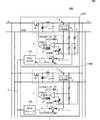
図1は第1の実施形態に係る電源システムの回路図である。この電源システム201は、複数の電源装置ユニット(以下、単に「ユニット」)100A,100B・・・を備え、それらの入力部および出力部がそれぞれ並列接続されて構成されている。図1では3つめ以降のユニットの図示は省略している。ユニット100A,100B・・・のそれぞれは基本的に同一構成であるが、この例では、ユニット100Aがマスター、他のユニット100B等はスレーブとして動作する。<< First Embodiment >>
FIG. 1 is a circuit diagram of a power supply system according to the first embodiment. The
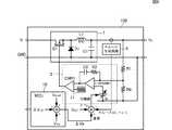
ユニット100Aを例に挙げると、ユニット100Aは、コンバータ部1、PWM制御部2、コントローラ10A、出力電圧検出回路3、出力電流検出回路5、ドループ生成回路6および加算回路7を備えている。コンバータ部1はスイッチ素子Q1、ダイオードD1、インダクタL1およびキャパシタC1を備えて、非絶縁の降圧コンバータ回路を構成している。PWM制御部2は、誤差増幅器OPAMP1,PWMコンパレータCMP1、三角波生成回路21を備えている。 Taking
出力電圧検出回路3は抵抗R1,R0による分圧回路である。誤差増幅器OPAMP1は目標値Vrと出力電圧検出回路3の出力電圧とを比較し、誤差電圧をPWMコンパレータCMP1の非反転端子へ与える。誤差増幅器OPAMP1の反転入力端と出力端との間には、キャパシタC2および抵抗R2が接続されている。この回路は制御系の発振防止のための位相補償回路として作用する。 The output
三角波生成回路21はPWM変調用の三角波信号を発生し、これをPWMコンパレータCMP1の反転端子へ与える。PWMコンパレータCMP1は、非反転端子への入力電圧と三角波信号とを比較することでPWM変調信号をスイッチ素子Q1へ与える。PWM制御部2は本発明に係る「定電圧制御部」に相当する。 The triangular
ドループ生成回路6はユニット100Aの出力電流Ioを検出し、出力電流Ioが大きくなるにともなって出力電圧を小さくする電圧電流特性、すなわちドループ特性をもたせるためのドループ用補正値ΔVoを生成する回路である。加算回路7は、コントローラ10Aから出力される出力電圧補正指令値Vmodを基準目標値Vrefに加算し、上記ドループ用補正値ΔVoを減算することで目標値Vrを定める。この目標値Vrが誤差増幅器OPAMP1の非反転入力端に与えられる。 The
コントローラ10AはマイクロコントロールユニットMCUで構成されている。コントローラ10Aは出力電圧補正指令値Vmodを算出する。コントローラ10Aおよび加算回路7は本発明に係る「出力電圧変更部」に相当する。 The
スイッチ素子Q1は上記PWM変調された信号で制御される。スイッチ素子Q1のオン期間にインダクタL1に励磁電流が流れ、オフ期間にダイオードD1を通して還流電流が流れる。 The switch element Q1 is controlled by the PWM modulated signal. An exciting current flows through the inductor L1 during the ON period of the switch element Q1, and a return current flows through the diode D1 during the OFF period.
コントローラ10Aはシリアルバス4を介して、通信相手のユニットのコントローラ(10B等)に対して、出力電圧補正指令値Vmodを伝送する。コントローラ10Aは本発明に係る「出力電圧補正指令部」に相当する。 The
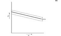
図2はユニットからの出力電流に対する出力電圧の関係を示す図である。実線はコントローラ10Aが定めた出力電圧補正指令値Vmodが或る値であるとき、ドループ生成回路6の作用による特性である。すなわち、出力電流Ioが増大するほど、出力電圧Voは一定勾配で減少する。コントローラ10Aが定めた出力電圧補正指令値Vmodが増減すると、それに伴い、図2の破線で示すとおり、上記ドループ特性を示すラインは傾き一定のまま上下にΔVc移動する。すなわち、ドループ特性の傾き自体は変化しないが、所定の出力電流における出力電圧レベルは変化する。上記ΔVcは出力電圧補正指令値Vmodの比例値である。 FIG. 2 is a diagram showing the relationship of the output voltage with respect to the output current from the unit. A solid line is a characteristic due to the action of the
図3は上記出力電圧補正指令値Vmodとドループ特性との関係を示す図である。上記出力電圧補正指令値Vmodは、この電圧上昇とドループ特性による電圧降下が相殺するように設定する。すなわち、出力電流Ioが増大するほど上記出力電圧補正指令値Vmodを大きくし、図3において電圧一定の破線で示すように、出力電流によらず出力電圧が一定となるようにする。この出力電流に対する上記出力電圧補正指令値Vmodは、Vmod=a・Ioの関係をテーブルまたは関数式でコントローラに設定しておく。 FIG. 3 is a diagram showing the relationship between the output voltage correction command value Vmod and the droop characteristic. The output voltage correction command value Vmod is set so that the voltage increase and the voltage drop due to the droop characteristic cancel each other. That is, as the output current Io increases, the output voltage correction command value Vmod is increased so that the output voltage becomes constant regardless of the output current, as indicated by a broken voltage constant line in FIG. For the output voltage correction command value Vmod for this output current, the relationship of Vmod = a · Io is set in the controller by a table or a function expression.
図4はマスターとして動作するコントローラ10Aおよびスレーブとして動作するコントローラ10Bの、各コントローラ内の回路または機能をブロック化して表した図である。コントローラ10Aにおいて、ADコンバータ13は、出力電流Ioの大きさを表す電圧信号を入力してディジタルデータに変換する。テーブル14は、ADコンバータ13により求められた値を基に、出力電圧補正指令値Vmodを生成する。また、シリアル通信部12は、この出力電圧補正指令値Vmodをデータとして他のコントローラ(10B等)へシリアルバス4を介して伝送する。DAコンバータ11は出力電圧補正指令値Vmodを電圧信号に変換してユニット100A内の加算回路7へ出力する。 FIG. 4 is a block diagram of circuits or functions in each controller of the
コントローラ10Bにおいて、シリアル通信部12はシリアルバス4を介して上記出力電圧補正指令値Vmodを受信し、DAコンバータ11は出力電圧補正指令値Vmodを電圧信号に変換してユニット100B内の加算回路7へ出力する。 In the
コントローラ10Aは、出力電流Ioの変動に対応するため、出力電流Ioの検出、出力電圧補正指令値Vmodの算出およびシリアル通信による指令を定期的または断続的に繰り返し行う。 The
以上に示したように、出力電圧の変更はユニット内の各コントローラが行うのではなく、1つのコントローラが他のコントローラに指令する。すなわち複数のコントローラのうち1つのコントローラが他のコントローラへ出力電圧の変更の指令を行うマスターとなる。マスターはシリアル通信でスレーブへ出力電圧補正指令値Vmodを送信し、これを受信したスレーブは指令値Vmodに基づいて出力電圧を変更する。同時にマスターもスレーブと同様に出力電圧を変更する。上記出力電圧補正指令値Vmodの指令の際はブロードキャスト送信(一斉送信)を用いれば、複数のコントローラへ一斉に指令することができる。また、シリアル通信にエラー検出やエラー訂正を適用することでノイズによるエラーを低減できる。 As described above, the change of the output voltage is not performed by each controller in the unit, but one controller commands another controller. That is, one of the plurality of controllers serves as a master that instructs other controllers to change the output voltage. The master transmits the output voltage correction command value Vmod to the slave by serial communication, and the slave that has received the command changes the output voltage based on the command value Vmod. At the same time, the master changes the output voltage in the same way as the slave. When the output voltage correction command value Vmod is commanded, a plurality of controllers can be commanded simultaneously by using broadcast transmission (simultaneous transmission). Moreover, errors due to noise can be reduced by applying error detection and error correction to serial communication.
このように、すべての電源ユニットで出力電圧の変更が同時に行われることにより、すべてのユニットが、同じ傾き及び同じ電圧レベルのドループ特性となる。これにより、各ユニットの出力電流はバランスする。 As described above, since the output voltage is changed simultaneously in all the power supply units, all the units have the droop characteristics having the same slope and the same voltage level. Thereby, the output current of each unit is balanced.
また、出力電流Ioの変動に応じてドループ特性により出力電圧Voは変動しようとするが、上記出力電圧補正指令値Vmod分の補正により、出力電圧Voの変動は相殺される。 Further, although the output voltage Vo tends to fluctuate due to the droop characteristic according to the fluctuation of the output current Io, the fluctuation of the output voltage Vo is canceled by the correction for the output voltage correction command value Vmod.
本実施形態によれば、電源システムのロードレギュレーション特性を低下させることなく、また、電流バランス端子を設けることもなく、出力電流を均等にすることができる。また、マスターからスレーブへの片方向通信でよいので、通信回線および通信制御の負荷が小さい。 According to the present embodiment, the output current can be equalized without degrading the load regulation characteristics of the power supply system and without providing a current balance terminal. In addition, since one-way communication from the master to the slave is sufficient, the load on the communication line and communication control is small.
なお、上記「出力電流」は、マスターのユニット100Aの出力電流または電源システム201全体の出力電流のいずれであってもよい。電源システム201全体の出力電流は、各電源ユニットがコントローラで検出した出力電流を、シリアル通信を介して取得し、それらを合計することで得られる。 The “output current” may be either the output current of the
本実施形態では、出力電圧を変更するために、PWM変調を行う目標値Vrを変更するように構成したが、出力電圧検出回路3側を制御してもよい。例えば、誤差増幅器OPAMP1の非反転入力端に抵抗を介してDAコンバータを接続し、それに制御信号を与えてもよい。 In the present embodiment, in order to change the output voltage, the target value Vr for PWM modulation is changed, but the output
《第2の実施形態》
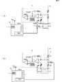
図5は第2の実施形態に係る電源システムの回路図である。この電源システム202は、第1の実施形態と異なり、マスターのコントローラ10Aが出力電流ではなく出力電圧を検出する。電源ユニット100Aは、出力電圧検出回路8を備えている。コントローラ10Aは出力電圧検出回路8の検出信号を入力する。コントローラ10Aの機能については次に示す。その他の構成は第1の実施形態と同じである。<< Second Embodiment >>
FIG. 5 is a circuit diagram of a power supply system according to the second embodiment. In the
図6はマスターとして動作するコントローラ10Aおよびスレーブとして動作するコントローラ10Bの、各コントローラ内の回路または機能をブロック化して表した図である。コントローラ10Aにおいて、ADコンバータ13は、出力電圧Voの大きさを表す電圧信号を入力してディジタルデータに変換する。加算回路15は、目標出力値Vo_refと出力電圧Voとの差(出力電圧誤差)evを求める。位相補償回路16は、この出力電圧誤差evを基に、出力電圧補正指令値Vmodを生成する。また、シリアル通信部12は、この出力電圧補正指令値Vmodをデータとして他のコントローラ(10B等)へ伝送する。DAコンバータ11は出力電圧補正指令値Vmodを電圧信号に変換してユニット100A内の加算回路7へ出力する。 FIG. 6 is a block diagram of circuits or functions in each controller of the
コントローラ10Bにおいて、シリアル通信部12はシリアルバスを介して上記出力電圧補正指令値Vmodを受信し、DAコンバータ11は出力電圧補正指令値Vmodを電圧信号に変換してユニット100B内の加算回路7へ出力する。 In the
コントローラ10Aは、出力電圧Voの変動に対応するため、出力電圧Voの検出、出力電圧補正指令値Vmodの算出およびシリアル通信による指令は定期的または断続的に繰り返し行う。 Since the
上記位相補償回路16は、出力電圧Voを制御量、前記出力電圧補正指令値Vmodを操作量とするフィードバック制御が行われるように伝達関数が定められている。この位相補償回路16の伝達関数は、K(s) = Kp + KI/ s + KDs で表される。ここでKpは比例要素の係数、KIは積分要素の係数、KDは微分要素の係数である。このようにしてPIDのフィードバック制御(またはKDをゼロとしたPIのフィードバック制御)を行うことが好ましい。The
本実施形態の場合も、出力電圧の変更はユニット内の各コントローラが行うのではなく、1つのコントローラが他のコントローラに指令する。すなわち複数のコントローラのうち1つのコントローラが他のコントローラへ出力電圧の変更の指令を行うマスターとなる。マスターはシリアル通信でスレーブへ出力電圧補正指令値Vmodを送信し、これを受信したスレーブは指令値Vmodに基づいて出力電圧を変更する。同時にマスターもスレーブと同様に出力電圧を変更する。上記出力電圧補正指令値Vmodの指令の際はブロードキャスト送信を用いれば、複数のコントローラへ一斉に指令をすることができる。また、シリアル通信にエラー検出やエラー訂正を適用することでノイズによるエラーを低減できる。 Also in this embodiment, the output voltage is not changed by each controller in the unit, but one controller commands another controller. That is, one of the plurality of controllers serves as a master that instructs other controllers to change the output voltage. The master transmits the output voltage correction command value Vmod to the slave by serial communication, and the slave that has received the command changes the output voltage based on the command value Vmod. At the same time, the master changes the output voltage in the same way as the slave. When the output voltage correction command value Vmod is instructed, it is possible to instruct a plurality of controllers all at once by using broadcast transmission. Moreover, errors due to noise can be reduced by applying error detection and error correction to serial communication.
このように、すべての電源ユニットで出力電圧増加が同時に行われることにより、すべてのユニットが、同じ傾き及び同じ電圧レベルのドループ特性となる。これにより、各ユニットの出力電流はバランスする。 As described above, since the output voltage is increased simultaneously in all the power supply units, all the units have the droop characteristic having the same slope and the same voltage level. Thereby, the output current of each unit is balanced.
また、出力電流Ioの変動に応じてドループ特性により出力電圧Voは変動しようとするが、上記フィードバック制御により、出力電圧Voは安定化される。 Further, although the output voltage Vo tends to change due to the droop characteristic according to the change of the output current Io, the output voltage Vo is stabilized by the feedback control.
本実施形態によれば、出力電圧がフィードバック制御されるため,出力電圧の精度が高めることができる。 According to this embodiment, since the output voltage is feedback controlled, the accuracy of the output voltage can be improved.
《第3の実施形態》
図7は第3の実施形態に係る電源システムの回路図である。この電源システム203は、第1・第2の実施形態と異なり、電源ユニット100A,100B以外に外部コントローラ20を備えている。また、電源システム203の出力電流Ioを検出する出力電流検出回路9を備えている。この外部コントローラ20の構成は、図4に示したコントローラ10AからDAコンバータ11を除いたものである。外部コントローラ20は電源システム203の出力電流の検出値を入力し、第1の実施形態で示したコントローラ10Aと同様の動作を行う。このように、コントローラをユニットの外部に設けてもよい。<< Third Embodiment >>
FIG. 7 is a circuit diagram of a power supply system according to the third embodiment. Unlike the first and second embodiments, the
また、このコントローラを外部に設ける形態を第2の実施形態で示した電源システムに適用してもよい。すなわち、その場合の外部コントローラは、図6に示したコントローラ10AからDAコンバータ11を除いたものである。この外部コントローラは出力電圧の検出値を入力し、第2の実施形態で示したコントローラ10Aと同様の動作を行う。 Further, a form in which this controller is provided outside may be applied to the power supply system shown in the second embodiment. That is, the external controller in that case is obtained by removing the
《第4の実施形態》
図8は第4の実施形態に係る電源システムのブロック図である。この電源システム204は、複数の電源ユニット100を備え、それらの入力部および出力部がそれぞれ並列接続され、構成されている。各電源ユニット100はコンバータ部とコントローラ10を備えている。各電源ユニット100の基本構成は同一であるが、1つの電源ユニットのコントローラ10がマスターとして動作し、他の電源ユニットのコントローラ10がスレーブとして動作する。<< Fourth Embodiment >>
FIG. 8 is a block diagram of a power supply system according to the fourth embodiment. The
本実施形態では、マスター動作するコントローラ10へシリアルバス41を介して負荷から出力電圧変更指令値ΔVrefが送信され、マスター動作するコントローラ10はスレーブ動作する複数のコントローラ10へシリアルバス42を介して出力電圧変更指令値ΔVrefが送信される。 In the present embodiment, the output voltage change command value ΔVref is transmitted from the load to the
図9は上記電源システム204が備える1つの電源ユニット100の回路図である。本実施形態の電源システムは、ドループ特性生成部による出力電圧の低下を補う目的とは別に、指令により出力電圧を変更できるようにした電源システムである。本実施形態において、出力電圧変更指令値ΔVrefは、図8において負荷または他の電源ユニットのコントローラ10から指令された値であるが、ドループ特性生成部による出力電圧の低下を補う目的の出力電圧変更指令値ではない。出力電圧を所定範囲内で任意に設定するための値である。 FIG. 9 is a circuit diagram of one
コントローラ10は、出力電圧変更指令値ΔVrefに、ドループ特性生成部による出力電圧の低下を補う補正値Vmodおよびキャリブレーション用の補正値Vcalを加算した値である目標値変更量ΔVaを目標値変更部へ与える。これにより出力電圧が変更される。なお、キャリブレーション用の補正値Vcalは、出力電圧変更の精度をより向上させるため、出荷時に工場において書き込まれる値である。 The
《第5の実施形態》
第5の実施形態では、目標値変更部に対して目標値を与える他の構成例を示す。<< Fifth Embodiment >>
In the fifth embodiment, another configuration example in which the target value is given to the target value changing unit is shown.
図10(A)(B)は第5の実施形態に係る目標値変更部の構成を示す図である。図10(A)の例では、コントローラ10はPWM制御部2へ、基準目標値Vrefと出力電圧変更指令値ΔVrefを合計した目標値を出力する。以上に示した各実施形態では、基準目標値Vrefを変更して目標値を定める加算回路7をアナログ回路的に表したが、本実施形態では、この変更をコントローラ10内でディジタル処理によって行う。 FIGS. 10A and 10B are diagrams showing the configuration of the target value changing unit according to the fifth embodiment. In the example of FIG. 10A, the
なお、図9に示したように、ドループ用補正値Vmodおよびキャリブレーション用補正値Vcalも考慮する場合には、コントローラ10は、
Vref+ΔVref+Vmod+Vcal
の演算を行い、その結果をDA変換してアナログ電圧としての目標値を出力すればよい。As shown in FIG. 9, when the droop correction value Vmod and the calibration correction value Vcal are also considered, the
Vref + ΔVref + Vmod + Vcal
And the result is DA converted to output a target value as an analog voltage.
図10(B)の例では、誤差増幅器OPAMP1の非反転入力端に基準電圧を印加し、反転入力端に出力電圧検出回路3の検出信号を入力するとともに、この反転入力端への入力電圧に、抵抗を介して目標値の反転信号を重畳する。このように出力電圧の検出値側を変化させてもよい。 In the example of FIG. 10B, the reference voltage is applied to the non-inverting input terminal of the error amplifier OPAMP1, the detection signal of the output
なお、図10(A)(B)いずれの構成においても、ドループ特性を持たせるためのドループ生成回路6の出力電圧を誤差増幅器OPAMP1の反転入力端側に入力する構成としてもよい。その場合には、出力電流変化に対する出力電圧変化の方向を逆の関係にする。 10A and 10B, the output voltage of the
《第6の実施形態》
第6の実施形態では、目標値をPWMにより出力する構成例を示す。<< Sixth Embodiment >>
The sixth embodiment shows a configuration example in which the target value is output by PWM.
図11は目標値変更部に対して与える目標値の電圧信号を発生する構成を示す図である。図11に示すコントローラ10は、ドループ特性を持たせるためのドループ用補正値以外の目標値に相当するPWM信号を出力する。その出力端子には抵抗RおよびコンデンサCによる平滑回路およびバッファ回路Bが接続されている。 FIG. 11 is a diagram showing a configuration for generating a voltage signal having a target value given to the target value changing unit. The
目標値の変更を高分解能で行うためには、図10(A)(B)に示したDA変換や図11に示したPWMを高分解能にする必要がある。しかし高分解能なDAコンバータやPWMを用いると、コスト高になる。さらに、PWMおよび平滑回路によって目標値のアナログ信号を発生させると、PWMの周期を長くしないと所定の電圧分解能が確保できない。そのため、応答性が悪化する。例えば、時間軸上の最小単位が10nsの場合、PWM分解能を10段階にするには、PWM周期としては100ns必要であり、PWM分解能を100段階にするには、PWM周期としては1000ns必要である。PWM信号は平滑フィルタで平滑されるため、周期が長くなると、それに応じて平滑フィルタの時定数が大きくなり、出力電圧の変更を高速に行えなくなる。 In order to change the target value with high resolution, the DA conversion shown in FIGS. 10A and 10B and the PWM shown in FIG. 11 need to have high resolution. However, using a high-resolution DA converter or PWM increases the cost. Furthermore, when an analog signal having a target value is generated by the PWM and smoothing circuit, a predetermined voltage resolution cannot be ensured unless the PWM cycle is lengthened. Therefore, responsiveness deteriorates. For example, when the minimum unit on the time axis is 10 ns, it takes 100 ns as the PWM cycle to set the PWM resolution to 10 steps, and 1000 ns as the PWM cycle to set the PWM resolution to 100 steps. . Since the PWM signal is smoothed by the smoothing filter, when the period becomes longer, the time constant of the smoothing filter increases accordingly, and the output voltage cannot be changed at high speed.
上記問題を解消するため、本実施形態では、上記目標値に相当する信号をディザリングしたDA変換またはPWMにより発生させ、目標値の変更を高分解能で行う。 In order to solve the above problem, in the present embodiment, a signal corresponding to the target value is generated by DA dithering or PWM that is dithered, and the target value is changed with high resolution.
図12はコントローラ10によるディザリングPWMの例を示す波形図である。ここで三角波状に変化する「タイマカウンタ」はコントローラ10内のタイマカウンタの値、「周期コンペア」はタイマカウンタの値と比較する値であり、タイマカウンタの値は周期コンペアの値に達したときクリアされる。これにより、タイマカウンタの値は三角波状に繰り返し変化する。「デューティコンペア」はタイマカウンタに対する比較対象の値である。この例では、M→M→M+1→M+1→M+1→N→N+1→N+1の順に変位している。「DMA転送用メモリ[1]〜[5]」はDMA(Direct Memory Access)転送用に確保されたメモリの値を示している。「タイマ割り込み」は一定周期で発生される割り込み信号、「DMA割り込み」は一定周期で発生されるDMA転送のための割り込み信号である。この例ではタイマ割り込み5回に1回の割合で発生される。「PWM出力」はタイマカウンタの値とデューティコンペアの値との比較結果の2値信号である。 FIG. 12 is a waveform diagram showing an example of dithering PWM by the
本実施形態のディザリングPWMの動作は次のとおりである。 The operation of the dithering PWM of this embodiment is as follows.
タイマカウンタは常に一定タイミングでインクリメントされ、周期コンペアと一致するとゼロにクリアされる。 The timer counter is always incremented at a constant timing, and cleared to zero when it coincides with the period compare.
タイマカウンタがデューティコンペア未満であるとPWM出力をH(ハイ)、デューティコンペア以上であるとPWM出力はL(ロー)となる。すなわち、デューティコンペアを変化させることでPWMのデューティを変更する。 If the timer counter is less than the duty compare, the PWM output is H (high), and if it is greater than or equal to the duty compare, the PWM output is L (low). In other words, the PWM duty is changed by changing the duty compare.
DMAコントローラは、タイマカウンタがゼロにクリアされると発生するタイマ割り込みをトリガとして、DMA転送用メモリ[1]〜[5]に格納されているデータをデューティコンペアへ順に転送する。 The DMA controller sequentially transfers the data stored in the DMA transfer memories [1] to [5] to the duty compare with a timer interrupt generated when the timer counter is cleared to zero as a trigger.
DMAコントローラはDMA転送メモリの個数(またはその整数倍)毎にDMA割り込みを行い、DMA転送用メモリの内容を更新する。 The DMA controller performs a DMA interrupt for each number of DMA transfer memories (or an integer multiple thereof) to update the contents of the DMA transfer memory.
実効デューティの整数部をi、小数部をdで表すと、DMA転送用メモリに格納される値はiまたはi+1であり、iとi+1の数の比はd/10に最も近い値である。例えば、実効デューティが15.6の場合、i=15、d=6であり、DMA転送用メモリには、iが2個、i+1が3個格納される。 When the integer part of the effective duty is represented by i and the decimal part is represented by d, the value stored in the DMA transfer memory is i or i + 1, and the ratio of the number of i and i + 1 is closest to d / 10 Value. For example, when the effective duty is 15.6, i = 15 and d = 6, and two i and three i + 1 are stored in the DMA transfer memory.
図13は出力電圧VoとPWMデューティとの関係を示す図である。この出力電圧VoとPWMデューティとの関係はテーブルに予め設定されている。例えば、現在の出力電圧Voが12.7Vであり、ドループ用補正値ΔVoが0.3Vになったとき、このドループによる出力電圧の低下を補って、出力電圧を13Vにするためには、PWMデューティを15.6にする。PWMデューティが15.6であるときのディザリングPWMの動作は既に示したとおりである。 FIG. 13 is a diagram showing the relationship between the output voltage Vo and the PWM duty. The relationship between the output voltage Vo and the PWM duty is preset in the table. For example, when the current output voltage Vo is 12.7V and the droop correction value ΔVo becomes 0.3V, in order to compensate for the drop in the output voltage due to the droop and to set the output voltage to 13V, the PWM duty is set to Set to 15.6. The operation of the dithering PWM when the PWM duty is 15.6 is as already described.
以上に示したディザリングPWMにより目標値を出力することにより、次のような効果を奏する。 By outputting the target value by the dithering PWM described above, the following effects can be obtained.
(1)ディザリングをハードウェアで構成しなくてもよいため、特別なハードウェアは不要である。またディザリング周期をソフトウェアで変更できるなど柔軟性が高い。(1) Since dithering does not have to be configured by hardware, no special hardware is required. The dithering cycle can be changed by software.
(2)PWM毎に処理を行う必要はないため、CPUの処理負荷は軽い。(2) Since it is not necessary to perform processing for each PWM, the processing load on the CPU is light.
(3)コンバータのスイッチング制御信号を生成するPWMに直接ディザリングを適用すると、コンバータの出力(電圧や電流)にディザリングの影響が現れることがあるのに対し、上記のように、PWM制御部2へ与える信号にディザリングを適用する場合には、コンバータの出力の前にRCフィルタや制御回路が介在するため、ディザリングの影響は出力に現れない。(3) When direct dithering is applied to the PWM that generates the switching control signal of the converter, the influence of dithering may appear on the output (voltage or current) of the converter. When dithering is applied to the signal applied to 2, since the RC filter and the control circuit are interposed before the output of the converter, the influence of dithering does not appear in the output.
なお、コントローラ10は基準目標値Vrefと出力電圧変更指令値ΔVrefを加算した目標値を発生するものに限らない。例えば、図1、図5、図7に示した出力電圧補正値VmodをディザリングPWMにより発生してもよいし、図9に示した目標値変更量ΔVaをディザリングPWMにより発生してもよい。 The
以上に示した例はPWMでのディザリングによる高分解能化の例を示したが、DAコンバータで、同様にディザリングにより高分解能化してもよい。すなわち、例えば図12に示したデータM→M→M+1→M+1→M+1→N→N+1→N+1の順にDA変換した信号を出力し、それを回路で平滑する。 Although the example shown above showed the example of the high resolution by the dithering in PWM, you may increase the resolution by the dithering similarly with a DA converter. That is, for example, the data M → M → M + 1 → M + 1 → M + 1 → N → N + 1 → N + 1 in the order shown in FIG. 12 is output, and the signal is smoothed by the circuit. .
《第7の実施形態》
第7の実施形態では、各電源ユニットのコントローラの同期動作について示す。<< Seventh Embodiment >>
In the seventh embodiment, the synchronous operation of the controller of each power supply unit will be described.
図14は第7の実施形態に係る電源システムの各部の波形図である。電源システムの回路構成は図8に示したとおりである。例えば図8に示した電源システム204において、電源ユニット100のマスター動作するコントローラ10は負荷と通信〈通信1〉して、負荷から出力電圧変更指令値ΔVrefを受信する。この〈通信1〉はマスター動作するコントローラ10から一定周期または所定タイミングで行われる。この〈通信1〉はコントローラ10から負荷への要求、または負荷からコントローラ10への要求で開始される。 FIG. 14 is a waveform diagram of each part of the power supply system according to the seventh embodiment. The circuit configuration of the power supply system is as shown in FIG. For example, in the
上記〈通信1〉とは別に、〈通信2〉により、出力電圧変更指令値ΔVrefの指令、出力のオン/オフの指令、スレーブ動作するコントローラ10の情報の取得等が一定周期で行われる。 In addition to the above <
マスター動作するコントローラ10はスレーブ動作するコントローラ10へ〈通信2〉により、出力電圧変更指令値を一斉に与えると、各電源ユニット100の目標値変更部は、出力電圧変更指令値の通信(受信)が終了した後、目標値を一斉に変更する。このとき、マスター動作するコントローラ10を含む電源ユニット100の目標値変更部も、出力電圧変更指令値の通信(送信)が終了した後、目標値を変更する。 When the
図14において、時刻t1での〈通信2〉で出力電圧変更指令値が変更され、それに伴い、時刻t2で出力電圧Voが変化している。このタイムラグTlは、各電源ユニット100のコントローラ10が出力電圧変更指令値の通信が終了した後、目標値変更部が目標値を一斉に変更するまでに要する時間である。この時間は全ての電源ユニット100について同じであるので、各電源ユニット100の出力電圧は出力電圧変更指令値に応じて同時に変更される。 In FIG. 14, the output voltage change command value is changed at <
図15は、図14に示した破線で囲んだ部分の拡大図であり、上記クロック信号とデータ信号の波形図およびデータのパケットを示す図である。この例では、一連のデータ(パケット)は5つのデータバイトで成り立っている。先頭のデータ00はジェネラルコールアドレスであり、全てのスレーブに対するコマンドであることを示す。データ21は出力電圧変更の指令であることを示すコマンドである。これに続く2バイトのコードA101(01A1)は出力電圧変更指令値の値である。最後のデータ22は誤り検出バイトである。 FIG. 15 is an enlarged view of a portion surrounded by a broken line shown in FIG. 14, and shows a waveform diagram of the clock signal and data signal and a data packet. In this example, a series of data (packets) consists of five data bytes. The
このようにして、出力電圧変更指令に応じて全ての電源ユニット100が同期して出力電圧Voを変化させるので、電流バランスを保ったまま並列運転ができる。 Thus, since all the
《他の実施形態》
以上に示した各実施形態では、コンバータ部が非絶縁の降圧コンバータ回路である例を示したが、コンバータ部は昇圧コンバータや昇降圧コンバータであってもよい。また絶縁トランスを用いた絶縁型であってもよい。<< Other embodiments >>
In each of the embodiments described above, an example in which the converter unit is a non-insulated step-down converter circuit has been described. However, the converter unit may be a boost converter or a buck-boost converter. Further, an insulating type using an insulating transformer may be used.
また、以上に示した各実施形態では、定電圧制御部を誤差増幅器および受動素子の組み合わせで構成したアナログ制御の例を示したが、これをMCUで処理するディジタル制御としてもよい。 Further, in each of the embodiments described above, an example of analog control in which the constant voltage control unit is configured by a combination of an error amplifier and a passive element has been described.
また、図1,5,7等では、電源装置の通信部が複数線のバスラインを介して通信する例を示したが、通信に用いる線数は単線であってもよい。また、シリアルバスを用いた通信に限らない。 1, 5, 7, and the like show an example in which the communication unit of the power supply device communicates via a plurality of lines of bus lines, but the number of lines used for communication may be a single line. In addition, communication using a serial bus is not limited.
C1…キャパシタ
CMP1…PWMコンパレータ
D1…ダイオード
L1…インダクタ
OPAMP1…誤差増幅器
Q1…スイッチ素子
1…コンバータ部
2…PWM制御部
3…出力電圧検出回路
4…シリアルバス
5…出力電流検出回路
6…ドループ生成回路
7…加算回路
8…出力電圧検出回路
9…出力電流検出回路
10A,10B…コントローラ
11…DAコンバータ
12…シリアル通信部
13…ADコンバータ
14…テーブル
15…加算回路
16…位相補償回路
20…外部コントローラ
21…三角波生成回路
41,42…シリアルバス
100A,100B…電源ユニット
201〜204…電源システムC1 ... Capacitor CMP1 ... PWM comparator D1 ... Diode L1 ... Inductor OPAMP1 ... Error amplifier Q1 ...
Claims (10)
Translated fromJapanese前記電源装置は、電力変換を行うコンバータ部と、前記コンバータ部の出力電圧と基準電圧との比較結果により前記電源装置の出力電圧を一定に制御する定電圧制御部と、前記電源装置の出力電流を検出する出力電流検出部と、前記出力電流が大きくなるにともなって前記電源装置の出力電圧を小さくするドループ特性生成部と、通信相手の電源装置との間で通信を行う通信部と、出力電圧補正指令値に応じて前記電源装置の出力電圧を変更する出力電圧変更部を備え、
前記複数の電源装置のうち少なくとも1つの電源装置は、前記出力電圧補正指令値を算出し、前記通信部により前記通信相手の電源装置に前記出力電圧補正指令値を与える出力電圧補正指令部を備え、
前記出力電圧補正指令部は、少なくとも前記出力電圧補正指令値を、ディザリングしたDA変換またはPWMで発生させる、
電源システム。In a power supply system that includes a plurality of power supply devices, and whose input unit and output unit are connected in parallel,
The power supply device includes a converter unit that performs power conversion, a constant voltage control unit that controls the output voltage of the power supply device to be constant based on a comparison result between an output voltage of the converter unit and a reference voltage, andan output current of thepower supply device An output current detection unit that detects the output current, a droop characteristic generation unit that reducesthe output voltage of thepower supply device as the output current increases, a communication unit that performs communication with the power supply device of the communication partner, and an output An output voltage changing unit that changes the output voltage of thepower supply device according to a voltage correction command value;
At least one power supply device of the plurality of power supply devices includes an output voltage correction command unit that calculates the output voltage correction command value and gives the output voltage correction command value to the communication partner power supply device by the communication unit.,
The output voltage correction command unit generates at least the output voltage correction command value by dithered DA conversion or PWM;
Power system.
出力電圧補正指令値を算出し、前記複数の電源装置に前記出力電圧補正指令値を与える出力電圧補正指令部を備え、
前記電源装置は、電力変換を行うコンバータ部と、前記コンバータ部の出力電圧と基準電圧との比較結果により前記電源装置の出力電圧を一定に制御する定電圧制御部と、前記電源装置の出力電流を検出する出力電流検出部と、前記出力電流が大きくなるにともなって前記電源装置の出力電圧を小さくするドループ特性生成部と、通信相手の電源装置との間で通信を行う通信部と、前記出力電圧補正指令値に応じて前記電源装置の出力電圧を変更する出力電圧変更部を備え、
前記出力電圧補正指令部は、少なくとも前記出力電圧補正指令値を、ディザリングしたDA変換またはPWMで発生させる、
電源システム。In a power supply system that includes a plurality of power supply devices, and whose input unit and output unit are connected in parallel,
An output voltage correction command unit that calculates an output voltage correction command value and gives the output voltage correction command value to the plurality of power supply devices,
The power supply device includes a converter unit that performs power conversion, a constant voltage control unit that controls the output voltage of the power supply device to be constant based on a comparison result between an output voltage of the converter unit and a reference voltage, andan output current of thepower supply device An output current detection unit that detects the output current, a droop characteristic generation unit that decreasesthe output voltage of thepower supply device as the output current increases, a communication unit that communicates with the power supply device of the communication counterpart, An output voltage changing unit that changes the output voltage of thepower supply device according to an output voltage correction command value;
The output voltage correction command unit generates at least the output voltage correction command value by dithered DA conversion or PWM;
Power system.
前記電源装置は、電力変換を行うコンバータ部と、前記コンバータ部の出力電圧と目標値との比較結果により前記電源装置の出力電圧を一定に制御する定電圧制御部と、前記電源装置の出力電流を検出する出力電流検出部と、前記出力電流が大きくなるにともなって前記電源装置の出力電圧を小さくするドループ特性生成部と、通信相手の電源装置との間で通信を行う通信部と、出力電圧変更指令値に応じて前記目標値を変更する目標値変更部とを備え、
前記複数の電源装置のうち少なくとも1つの電源装置は、並列接続された他の電源装置に対して、前記通信部により前記出力電圧変更指令値を一斉に与える出力電圧変更指令部を備え、
前記並列接続された前記1つの電源装置および前記他の電源装置の前記目標値変更部は、前記出力電圧変更指令値の通信が終了した後、前記目標値を一斉に変更し、
前記出力電圧変更指令部は、少なくとも前記出力電圧変更指令値を、ディザリングしたDA変換またはPWMで発生させる、
電源システム。In a power supply system that includes a plurality of power supply devices, and whose input unit and output unit are connected in parallel,
The power supply device includes a converter unit that performs power conversion, a constant voltage control unit that controls the output voltage of the power supply device to be constant based on a comparison result between an output voltage of the converter unit and a target value, andan output current of thepower supply device An output current detection unit that detects the output current, a droop characteristic generation unit that reducesthe output voltage of thepower supply device as the output current increases, a communication unit that performs communication with the power supply device of the communication partner, and an output A target value changing unit that changes the target value according to a voltage change command value,
At least one power supply device among the plurality of power supply devices includes an output voltage change command unit that simultaneously gives the output voltage change command value by the communication unit to other power supply devices connected in parallel,
The target value change of the parallel-connected the one power supply and the other power supply, after the communication of the output voltage change command value is completed,to change the target value simultaneously,
The output voltage change command unit generates at least the output voltage change command value by dithered DA conversion or PWM,
Power system.
前記複数の電源装置に出力電圧変更指令値を一斉に与える出力電圧変更指令部を備え、
前記電源装置は、電力変換を行うコンバータ部と、前記コンバータ部の出力電圧と目標値との比較結果により前記電源装置の出力電圧を一定に制御する定電圧制御部と、前記電源装置の出力電流を検出する出力電流検出部と、前記出力電流が大きくなるにともなって前記電源装置の出力電圧を小さくするドループ特性生成部と、通信相手の電源装置との間で通信を行う通信部と、前記出力電圧変更指令値に応じて前記目標値を変更する目標値変更部とを備え、
前記複数の電源装置の前記目標値変更部は、前記出力電圧変更指令値の通信が終了した後、前記目標値を一斉に変更し、
前記出力電圧変更指令部は、少なくとも前記出力電圧変更指令値を、ディザリングしたDA変換またはPWMで発生させる、
電源システム。In a power supply system that includes a plurality of power supply devices, and whose input unit and output unit are connected in parallel,
An output voltage change command unit thatsimultaneously gives output voltage change command values to the plurality of power supply devices,
The power supply device includes a converter unit that performs power conversion, a constant voltage control unit that controls the output voltage of the power supply device to be constant based on a comparison result between an output voltage of the converter unit and a target value, andan output current of thepower supply device An output current detection unit that detects the output current, a droop characteristic generation unit that decreasesthe output voltage of thepower supply device as the output current increases, a communication unit that communicates with the power supply device of the communication counterpart, A target value changing unit that changes the target value according to an output voltage change command value;
Wherein said target value changing portion of the plurality of power supply after a communication of the output voltage change command value is completed,to change the target value simultaneously,
The output voltage change command unit generates at least the output voltage change command value by dithered DA conversion or PWM,
Power system.
前記出力電圧補正指令部は、前記電源システム出力電流検知部が検知した出力電流が大きくなるにともなって前記電源システムの出力電圧が大きくなるように前記出力電圧補正指令値を設定することにより、前記ドループ特性生成部による出力電圧の低下を補う、請求項2に記載の電源システム。Apower system output current detection unit for detecting or acquiring the output current of thepower system ;
The output voltage correction command unit sets the output voltage correction command value so that the output voltage of the power system increases as the output current detected by thepower system output current detector increases. The power supply system according to claim 2, which compensates for a decrease in output voltage caused by a droop characteristic generation unit.
前記出力電圧変更指令部は、前記電源システム出力電流検知部が検知した出力電流が大きくなるにともなって前記電源システムの出力電圧が大きくなるように前記出力電圧変更指令値を設定することにより、前記ドループ特性生成部による出力電圧の低下を補う、請求項4に記載の電源システム。Apower system output current detection unit for detecting or acquiring the output current of thepower system ;
The output voltage change command unit sets the output voltage change command value so that the output voltage of the power system increases as the output current detected by thepower system output current detector increases. The power supply system of Claim 4 which compensates for the fall of the output voltage by a droop characteristic production | generation part.
前記出力電圧補正指令部は、前記電源システムの出力電圧を制御量、前記電源システムの前記出力電圧補正指令値を操作量としてフィードバック制御されるように、前記出力電圧補正指令値を求める、請求項1または2に記載の電源システム。An output voltage detector for detecting an output voltage of the power supply system;
The output voltage correction command unit, the amount of control the output voltage of the power supply system, as feedback control ofthe output voltage correction command value of the power system as a manipulated variable, determiningthe output voltage correction command value, claim The power supply system according to 1 or 2.
前記出力電圧変更指令部は、前記電源システムの出力電圧を制御量、前記電源システムの前記出力電圧変更指令値を操作量としてフィードバック制御されるように、前記出力電圧変更指令値を求める、請求項3または4に記載の電源システム。An output voltage detector for detecting an output voltage of the power supply system;
The output voltage change instruction unit, the amount of control the output voltage of the power supply system, as feedback control ofthe output voltage change command value of the power system as a manipulated variable, determiningthe output voltage change command value, claim The power supply system according to 3 or 4.
Applications Claiming Priority (5)
| Application Number | Priority Date | Filing Date | Title |
|---|---|---|---|
| JP2013207254 | 2013-10-02 | ||
| JP2013207254 | 2013-10-02 | ||
| JP2013237284 | 2013-11-15 | ||
| JP2013237284 | 2013-11-15 | ||
| PCT/JP2014/075984WO2015050093A1 (en) | 2013-10-02 | 2014-09-30 | Power supply system |
Related Child Applications (1)
| Application Number | Title | Priority Date | Filing Date |
|---|---|---|---|
| JP2017087785ADivisionJP6296192B2 (en) | 2013-10-02 | 2017-04-27 | Power system |
Publications (2)
| Publication Number | Publication Date |
|---|---|
| JPWO2015050093A1 JPWO2015050093A1 (en) | 2017-03-09 |
| JP6206500B2true JP6206500B2 (en) | 2017-10-04 |
Family
ID=52778682
Family Applications (2)
| Application Number | Title | Priority Date | Filing Date |
|---|---|---|---|
| JP2015540488AActiveJP6206500B2 (en) | 2013-10-02 | 2014-09-30 | Power system |
| JP2017087785AActiveJP6296192B2 (en) | 2013-10-02 | 2017-04-27 | Power system |
Family Applications After (1)
| Application Number | Title | Priority Date | Filing Date |
|---|---|---|---|
| JP2017087785AActiveJP6296192B2 (en) | 2013-10-02 | 2017-04-27 | Power system |
Country Status (4)
| Country | Link |
|---|---|
| JP (2) | JP6206500B2 (en) |
| CN (1) | CN105580261A (en) |
| DE (1) | DE112014004589T5 (en) |
| WO (1) | WO2015050093A1 (en) |
Families Citing this family (25)
| Publication number | Priority date | Publication date | Assignee | Title |
|---|---|---|---|---|
| JP6609506B2 (en)* | 2016-04-11 | 2019-11-20 | 株式会社日立産機システム | Power converter |
| JP6650838B2 (en) | 2016-06-23 | 2020-02-19 | 株式会社ダイヘン | Power supply system, power supply, control method, and control program |
| JP2018082549A (en)* | 2016-11-16 | 2018-05-24 | サンケン電気株式会社 | Switching power supply device |
| JP6714519B2 (en)* | 2017-01-13 | 2020-06-24 | コーセル株式会社 | Switching power supply |
| JP6835676B2 (en) | 2017-07-05 | 2021-02-24 | 株式会社ダイヘン | Power system, power supply, control method and control program |
| JP7018847B2 (en)* | 2018-08-03 | 2022-02-14 | Ntn株式会社 | Switching power supply system and DC power supply system |
| JP7030033B2 (en)* | 2018-08-31 | 2022-03-04 | 株式会社デンソー | Power conversion system |
| CN110488901A (en)* | 2019-09-18 | 2019-11-22 | 深圳市友华通信技术有限公司 | The output voltage adjusting method and device of power module |
| JP7291592B2 (en)* | 2019-10-01 | 2023-06-15 | 日鉄テックスエンジ株式会社 | Converter device and its output control method |
| JP7200901B2 (en)* | 2019-10-03 | 2023-01-10 | 株式会社豊田自動織機 | power supply |
| JP7279852B2 (en) | 2020-04-15 | 2023-05-23 | 富士電機株式会社 | integrated circuit, power supply |
| US12119757B2 (en) | 2020-04-21 | 2024-10-15 | Mitsubishi Electric Corporation | Power supply system including a plurality of power conversion devices to supply AC or DC power |
| CN111628634A (en)* | 2020-06-19 | 2020-09-04 | 西安微电子技术研究所 | Output isolation power supply sampling circuit and method |
| WO2022030363A1 (en)* | 2020-08-05 | 2022-02-10 | パナソニックIpマネジメント株式会社 | Power system, controller, power conversion device, power system control method, and program |
| JP7489485B2 (en)* | 2020-11-06 | 2024-05-23 | 株式会社安川電機 | Power Conversion Systems |
| JP7634975B2 (en)* | 2020-11-30 | 2025-02-25 | 株式会社アドバンテスト | Power supplies, power supply units, test equipment |
| JP7561589B2 (en)* | 2020-11-30 | 2024-10-04 | 株式会社アドバンテスト | Power supplies, power supply units, test equipment |
| KR102828542B1 (en) | 2021-01-27 | 2025-07-02 | 가부시키가이샤 산샤덴키세이사쿠쇼 | Power Systems and Power Units |
| WO2022162764A1 (en) | 2021-01-27 | 2022-08-04 | 株式会社三社電機製作所 | Power supply system and power supply unit |
| US20240007327A1 (en)* | 2021-01-27 | 2024-01-04 | Sansha Electric Manufacturing Co., Ltd. | Power supply system and power supply unit |
| JP7602394B2 (en)* | 2021-02-16 | 2024-12-18 | 新電元工業株式会社 | Charging and discharging system |
| CN112821753A (en)* | 2021-02-25 | 2021-05-18 | 中国电子科技集团公司第十八研究所 | Multi-module power distribution topological circuit |
| JP7621146B2 (en) | 2021-03-18 | 2025-01-24 | ローム株式会社 | Power System |
| CN113346473A (en)* | 2021-05-25 | 2021-09-03 | 上海辛格林纳新时达电机有限公司 | Grid-connected control method and grid-connected control device |
| WO2024009638A1 (en)* | 2022-07-07 | 2024-01-11 | ローム株式会社 | Power supply system, semiconductor integrated circuit device, semiconductor device, and power supply device |
Family Cites Families (15)
| Publication number | Priority date | Publication date | Assignee | Title |
|---|---|---|---|---|
| JPS61262821A (en)* | 1985-05-15 | 1986-11-20 | Origin Electric Co Ltd | System for controlling power source output |
| JP2004328945A (en)* | 2003-04-28 | 2004-11-18 | Sharp Corp | PWM control circuit for DC-DC converter |
| US7304462B2 (en)* | 2005-02-02 | 2007-12-04 | Power-One, Inc. | Compensated droop method for paralleling of power supplies (C-droop method) |
| JP4538349B2 (en)* | 2005-03-17 | 2010-09-08 | 富士通株式会社 | Power supply and power supply system |
| JP5226399B2 (en)* | 2008-06-25 | 2013-07-03 | 新電元工業株式会社 | Power supply device and control method of power supply device |
| US8120205B2 (en)* | 2008-07-18 | 2012-02-21 | Zilker Labs, Inc. | Adding and dropping phases in current sharing |
| EP2333957B1 (en)* | 2009-12-04 | 2015-01-28 | Nxp B.V. | A clock signal generator |
| CN102122896A (en)* | 2011-04-15 | 2011-07-13 | 国网电力科学研究院 | Sine wave inverter parallel system with variable current ratio |
| JP5967871B2 (en)* | 2011-06-27 | 2016-08-10 | トランスフォーム・ジャパン株式会社 | Power supply |
| JP5792024B2 (en)* | 2011-10-21 | 2015-10-07 | 株式会社日本自動車部品総合研究所 | Power system |
| JP5802549B2 (en)* | 2011-12-28 | 2015-10-28 | コーセル株式会社 | Power supply device and power supply system using the same |
| CN103219885B (en)* | 2012-01-20 | 2015-08-12 | 百富(澳门离岸商业服务)有限公司 | DC to DC transducer |
| EP2823614B1 (en)* | 2012-03-07 | 2018-12-26 | Cirrus Logic International Semiconductor Ltd. | Signal conversion system and method |
| JP6019633B2 (en)* | 2012-03-12 | 2016-11-02 | シンフォニアテクノロジー株式会社 | Power converter |
| CN102594128A (en)* | 2012-04-05 | 2012-07-18 | 重庆安谐新能源技术有限公司 | Average current control device for direct current (DC) average current output system |
- 2014
- 2014-09-30JPJP2015540488Apatent/JP6206500B2/enactiveActive
- 2014-09-30WOPCT/JP2014/075984patent/WO2015050093A1/enactiveApplication Filing
- 2014-09-30CNCN201480052330.3Apatent/CN105580261A/enactivePending
- 2014-09-30DEDE112014004589.6Tpatent/DE112014004589T5/ennot_activeCeased
- 2017
- 2017-04-27JPJP2017087785Apatent/JP6296192B2/enactiveActive
Also Published As
| Publication number | Publication date |
|---|---|
| JP6296192B2 (en) | 2018-03-20 |
| JPWO2015050093A1 (en) | 2017-03-09 |
| CN105580261A (en) | 2016-05-11 |
| JP2017127195A (en) | 2017-07-20 |
| WO2015050093A1 (en) | 2015-04-09 |
| DE112014004589T5 (en) | 2016-08-18 |
Similar Documents
| Publication | Publication Date | Title |
|---|---|---|
| JP6296192B2 (en) | Power system | |
| JP5486954B2 (en) | Switching power supply | |
| US9473027B2 (en) | Voltage regulator with hybrid adaptive voltage position and control method thereof | |
| JP5788748B2 (en) | DC / DC converter control circuit and DC-DC converter | |
| JP6285235B2 (en) | Control circuit for digital control power supply circuit, control method, digital control power supply circuit using the same, electronic device and base station | |
| JP5625958B2 (en) | Switching power supply with output voltage switching function | |
| JP5808990B2 (en) | DC / DC converter control circuit and DC-DC converter | |
| JP5812777B2 (en) | DC / DC converter control circuit and DC-DC converter | |
| JP5902421B2 (en) | DC / DC converter control circuit and DC-DC converter | |
| JP5791582B2 (en) | Switching power supply device and power supply system using the same | |
| KR20070017501A (en) | Method and system for communicating filter compensation coefficient of digital power control system | |
| US10873259B2 (en) | Stable digital integrator circuit for boost converter | |
| US20080079406A1 (en) | Power supply with digital feedback loop | |
| TWI741625B (en) | Power conversion system for autonomous current sharing of power stages | |
| US20100301823A1 (en) | Power supply unit and control circuit of power supply unit | |
| CN107872150B (en) | Power supply device | |
| JP2021058042A (en) | Converter device and output control method of the same | |
| CN115276395A (en) | A power conversion circuit and related method | |
| CN110932524A (en) | Controller and Current Balancing Method for Multiphase Power Conversion | |
| US20170222549A1 (en) | Dc-dc converter including dynamically adjusted duty cycle limit | |
| CN112748757A (en) | DAC control logic for controlling a DAC | |
| TWI581550B (en) | Method for Controlling a Converter | |
| JP6191698B2 (en) | Power system | |
| CN119556758A (en) | A circuit for dynamically adjusting the output voltage of a DC voltage regulator | |
| JP2015198481A (en) | Power conversion system |
Legal Events
| Date | Code | Title | Description |
|---|---|---|---|
| A131 | Notification of reasons for refusal | Free format text:JAPANESE INTERMEDIATE CODE: A131 Effective date:20170228 | |
| A521 | Request for written amendment filed | Free format text:JAPANESE INTERMEDIATE CODE: A523 Effective date:20170427 | |
| TRDD | Decision of grant or rejection written | ||
| A01 | Written decision to grant a patent or to grant a registration (utility model) | Free format text:JAPANESE INTERMEDIATE CODE: A01 Effective date:20170808 | |
| A61 | First payment of annual fees (during grant procedure) | Free format text:JAPANESE INTERMEDIATE CODE: A61 Effective date:20170821 | |
| R150 | Certificate of patent or registration of utility model | Ref document number:6206500 Country of ref document:JP Free format text:JAPANESE INTERMEDIATE CODE: R150 |