JP6205598B2 - Display device - Google Patents
Display deviceDownload PDFInfo
- Publication number
- JP6205598B2 JP6205598B2JP2013525572AJP2013525572AJP6205598B2JP 6205598 B2JP6205598 B2JP 6205598B2JP 2013525572 AJP2013525572 AJP 2013525572AJP 2013525572 AJP2013525572 AJP 2013525572AJP 6205598 B2JP6205598 B2JP 6205598B2
- Authority
- JP
- Japan
- Prior art keywords
- electrode
- pixels
- electrode patterns
- display
- line
- Prior art date
- Legal status (The legal status is an assumption and is not a legal conclusion. Google has not performed a legal analysis and makes no representation as to the accuracy of the status listed.)
- Active
Links
Images


Classifications
- G—PHYSICS
- G06—COMPUTING OR CALCULATING; COUNTING
- G06F—ELECTRIC DIGITAL DATA PROCESSING
- G06F3/00—Input arrangements for transferring data to be processed into a form capable of being handled by the computer; Output arrangements for transferring data from processing unit to output unit, e.g. interface arrangements
- G06F3/01—Input arrangements or combined input and output arrangements for interaction between user and computer
- G06F3/03—Arrangements for converting the position or the displacement of a member into a coded form
- G06F3/041—Digitisers, e.g. for touch screens or touch pads, characterised by the transducing means
- G06F3/044—Digitisers, e.g. for touch screens or touch pads, characterised by the transducing means by capacitive means
- G06F3/0448—Details of the electrode shape, e.g. for enhancing the detection of touches, for generating specific electric field shapes, for enhancing display quality
- G—PHYSICS
- G06—COMPUTING OR CALCULATING; COUNTING
- G06F—ELECTRIC DIGITAL DATA PROCESSING
- G06F3/00—Input arrangements for transferring data to be processed into a form capable of being handled by the computer; Output arrangements for transferring data from processing unit to output unit, e.g. interface arrangements
- G06F3/01—Input arrangements or combined input and output arrangements for interaction between user and computer
- G06F3/03—Arrangements for converting the position or the displacement of a member into a coded form
- G06F3/041—Digitisers, e.g. for touch screens or touch pads, characterised by the transducing means
- G06F3/0412—Digitisers structurally integrated in a display
- G—PHYSICS
- G06—COMPUTING OR CALCULATING; COUNTING
- G06F—ELECTRIC DIGITAL DATA PROCESSING
- G06F3/00—Input arrangements for transferring data to be processed into a form capable of being handled by the computer; Output arrangements for transferring data from processing unit to output unit, e.g. interface arrangements
- G06F3/01—Input arrangements or combined input and output arrangements for interaction between user and computer
- G06F3/03—Arrangements for converting the position or the displacement of a member into a coded form
- G06F3/041—Digitisers, e.g. for touch screens or touch pads, characterised by the transducing means
- G06F3/044—Digitisers, e.g. for touch screens or touch pads, characterised by the transducing means by capacitive means
- G06F3/0445—Digitisers, e.g. for touch screens or touch pads, characterised by the transducing means by capacitive means using two or more layers of sensing electrodes, e.g. using two layers of electrodes separated by a dielectric layer
- G—PHYSICS
- G06—COMPUTING OR CALCULATING; COUNTING
- G06F—ELECTRIC DIGITAL DATA PROCESSING
- G06F3/00—Input arrangements for transferring data to be processed into a form capable of being handled by the computer; Output arrangements for transferring data from processing unit to output unit, e.g. interface arrangements
- G06F3/01—Input arrangements or combined input and output arrangements for interaction between user and computer
- G06F3/03—Arrangements for converting the position or the displacement of a member into a coded form
- G06F3/041—Digitisers, e.g. for touch screens or touch pads, characterised by the transducing means
- G06F3/044—Digitisers, e.g. for touch screens or touch pads, characterised by the transducing means by capacitive means
- G06F3/0446—Digitisers, e.g. for touch screens or touch pads, characterised by the transducing means by capacitive means using a grid-like structure of electrodes in at least two directions, e.g. using row and column electrodes
- H—ELECTRICITY
- H10—SEMICONDUCTOR DEVICES; ELECTRIC SOLID-STATE DEVICES NOT OTHERWISE PROVIDED FOR
- H10K—ORGANIC ELECTRIC SOLID-STATE DEVICES
- H10K59/00—Integrated devices, or assemblies of multiple devices, comprising at least one organic light-emitting element covered by group H10K50/00
- H10K59/40—OLEDs integrated with touch screens
- G—PHYSICS
- G02—OPTICS
- G02F—OPTICAL DEVICES OR ARRANGEMENTS FOR THE CONTROL OF LIGHT BY MODIFICATION OF THE OPTICAL PROPERTIES OF THE MEDIA OF THE ELEMENTS INVOLVED THEREIN; NON-LINEAR OPTICS; FREQUENCY-CHANGING OF LIGHT; OPTICAL LOGIC ELEMENTS; OPTICAL ANALOGUE/DIGITAL CONVERTERS
- G02F1/00—Devices or arrangements for the control of the intensity, colour, phase, polarisation or direction of light arriving from an independent light source, e.g. switching, gating or modulating; Non-linear optics
- G02F1/01—Devices or arrangements for the control of the intensity, colour, phase, polarisation or direction of light arriving from an independent light source, e.g. switching, gating or modulating; Non-linear optics for the control of the intensity, phase, polarisation or colour
- G02F1/13—Devices or arrangements for the control of the intensity, colour, phase, polarisation or direction of light arriving from an independent light source, e.g. switching, gating or modulating; Non-linear optics for the control of the intensity, phase, polarisation or colour based on liquid crystals, e.g. single liquid crystal display cells
- G02F1/133—Constructional arrangements; Operation of liquid crystal cells; Circuit arrangements
- G02F1/1333—Constructional arrangements; Manufacturing methods
- G02F1/13338—Input devices, e.g. touch panels
- G—PHYSICS
- G06—COMPUTING OR CALCULATING; COUNTING
- G06F—ELECTRIC DIGITAL DATA PROCESSING
- G06F2203/00—Indexing scheme relating to G06F3/00 - G06F3/048
- G06F2203/041—Indexing scheme relating to G06F3/041 - G06F3/045
- G06F2203/04103—Manufacturing, i.e. details related to manufacturing processes specially suited for touch sensitive devices
Landscapes
- Engineering & Computer Science (AREA)
- General Engineering & Computer Science (AREA)
- Theoretical Computer Science (AREA)
- Human Computer Interaction (AREA)
- Physics & Mathematics (AREA)
- General Physics & Mathematics (AREA)
- Quality & Reliability (AREA)
- Devices For Indicating Variable Information By Combining Individual Elements (AREA)
- Electroluminescent Light Sources (AREA)
- Position Input By Displaying (AREA)
Description
Translated fromJapanese本発明は、表示装置に関し、特に、ユーザが指やペン等を検出面(タッチ面)に接触または近接させたときに、指やペン等の位置を検出する検出装置(タッチパネル)を備えた表示装置に関する。 The present invention relates to a display device, and in particular, a display provided with a detection device (touch panel) that detects the position of a finger, a pen, or the like when a user brings a finger, a pen, or the like into contact with or close to a detection surface (touch surface) Relates to the device.
表示装置において、画面を見ながら簡単に入力などの操作をできるようにするため、従来、いわゆるタッチパネルがよく用いられている。 Conventionally, a so-called touch panel is often used in a display device so that an operation such as an input can be easily performed while viewing a screen.
タッチパネルは通常、表示パネルの一主面側(表示面側)に貼り付けられる。ユーザは、表示パネルの画面に表示されるボタンなどのオブジェクトをタッチパネルによって選択することで、表示パネルへの入力等の各種操作を行う。 The touch panel is usually attached to one main surface side (display surface side) of the display panel. The user performs various operations such as input to the display panel by selecting objects such as buttons displayed on the screen of the display panel using the touch panel.
例えば特許文献1には、表示パネルの前面にタッチパネルを一体配置して成る表示装置が開示されている。 For example,
近年、液晶ディスプレイ、プラズマディスプレイパネルまたは有機ELディスプレイ等の表示パネルの大画面化および高精細化に伴い、その表示パネルと組み合わせて使用されるタッチパネルについても、大型化および解像度の高精細化が進んでいる。 In recent years, with the increase in screen size and definition of a display panel such as a liquid crystal display, plasma display panel, or organic EL display, the touch panel used in combination with the display panel has also increased in size and resolution. It is out.
本発明は、このような状況に鑑みてなされたものであり、比較的大インチサイズ、高精細および良視認性である、タッチパネルを備えた表示装置を提供することを目的とする。 The present invention has been made in view of such a situation, and an object thereof is to provide a display device including a touch panel that has a relatively large inch size, high definition, and good visibility.
上述した目的を実現するために、本発明の一態様に係る表示装置は、行列状に配置された複数の画素を有する表示パネルと、前記表示パネルに対向するタッチパネルと、を備え、前記表示パネルは、隣り合う画素の間の領域である非表示部を有し、前記タッチパネルは、前記画素の行方向および前記画素の列方向のいずれか一方である第1方向に沿って形成され、少なくとも一部分が金属である複数の第1電極パターンと、前記画素の行方向および前記画素の列方向のいずれか他方である第2方向に沿って形成され、少なくとも一部分が金属である複数の第2電極パターンとを有し、前記複数の第1電極パターンおよび前記複数の第2電極パターンの前記金属の部分は、平面視において、前記表示パネルの前記非表示部内に存在することを特徴とする。 In order to achieve the above-described object, a display device according to one embodiment of the present invention includes a display panel having a plurality of pixels arranged in a matrix, and a touch panel facing the display panel, and the display panel Has a non-display portion that is a region between adjacent pixels, and the touch panel is formed along a first direction that is one of a row direction of the pixels and a column direction of the pixels, and is at least partially And a plurality of second electrode patterns that are formed along a second direction that is either the row direction of the pixels or the column direction of the pixels, and at least a portion of which is a metal. The metal portions of the plurality of first electrode patterns and the plurality of second electrode patterns are present in the non-display portion of the display panel in plan view. To.
本発明によれば、比較的大インチサイズ、高精細および良視認性である、タッチパネルを備えた表示装置を提供することができる。 ADVANTAGE OF THE INVENTION According to this invention, the display apparatus provided with the touchscreen which is a comparatively large inch size, high definition, and good visibility can be provided.
(本発明の一態様を得るに至った経緯)
近年、表示パネルの大画面化および高精細化が進んでおり、これに伴って、表示パネルと組み合わせて使用されるタッチパネルについても大画面化および高精細化が要求されている。(Background to obtaining one embodiment of the present invention)
In recent years, display panels have been increased in screen size and definition, and accordingly, a touch panel used in combination with the display panel is also required to have a large screen and high definition.
しかしながら、タッチパネルにおける指やペン等の位置を検出するための電極パターンとしては、例えばITO(Indium Tin Oxide)などの高抵抗の透明電極材料が用いられているので、タッチパネルを大画面化および高精細化して電極パターンの配線を長くしたり細くしたりすると、配線抵抗が大きくなってタッチ位置の検知感度が低下するという問題がある。 However, a high-resistance transparent electrode material such as ITO (Indium Tin Oxide), for example, is used as an electrode pattern for detecting the position of a finger, pen, etc. on the touch panel. If the electrode pattern wiring is made longer or thinner, there is a problem that the wiring resistance increases and the touch position detection sensitivity decreases.
一方、配線抵抗を小さくするために、タッチパネルの電極パターンとして低抵抗材料であるアルミニウムや銅などの金属を用いると、表示パネルに表示される画像が金属によって遮光される場合があり、画像の視認性が低下するという問題がある。 On the other hand, if a metal such as aluminum or copper, which is a low-resistance material, is used as the electrode pattern of the touch panel in order to reduce the wiring resistance, the image displayed on the display panel may be shielded from light by the metal. There is a problem that the performance is lowered.
このような問題を解決するために、本発明の一態様に係る表示装置は、行列状に配置された複数の画素を有する表示パネルと、前記表示パネルに対向するタッチパネルと、を備え、前記表示パネルは、隣り合う画素の間の領域である非表示部を有し、前記タッチパネルは、前記画素の行方向および前記画素の列方向のいずれか一方である第1方向に沿って形成され、少なくとも一部分が金属である複数の第1電極パターンと、前記画素の行方向および前記画素の列方向のいずれか他方である第2方向に沿って形成され、少なくとも一部分が金属である複数の第2電極パターンとを有し、前記複数の第1電極パターンおよび前記複数の第2電極パターンの前記金属の部分は、平面視において、前記表示パネルの前記非表示部内に存在することを特徴とする。 In order to solve such a problem, a display device according to one embodiment of the present invention includes a display panel including a plurality of pixels arranged in a matrix, and a touch panel facing the display panel, and the display The panel has a non-display portion that is an area between adjacent pixels, and the touch panel is formed along a first direction that is one of a row direction of the pixels and a column direction of the pixels, and at least A plurality of first electrode patterns that are partially metal, and a plurality of second electrodes that are formed along a second direction that is either the row direction of the pixels or the column direction of the pixels, and at least a portion of which is metal. The metal portions of the plurality of first electrode patterns and the plurality of second electrode patterns are present in the non-display portion of the display panel in plan view. And butterflies.
本態様によれば、タッチパネルにおける第1電極パターンおよび第2電極パターンに、低抵抗材料である金属が用いられているので、高抵抗材料である透明電極材料のみで第1電極パターンおよび第2電極パターンを構成する場合と比べて、第1電極パターンおよび第2電極パターンの配線抵抗を小さくすることができる。これにより、タッチパネルの大画面化および高精細化を容易に実現することができる。また、第1電極パターンおよび第2電極パターンの金属部分が表示パネルの非表示部内に存在しているので、第1電極パターンおよび第2電極パターンの金属部分によって表示パネルの画像が遮光されてしまうことを抑制することができる。これにより、画像の視認性が低下することを抑制することができる。さらに、第1電極パターンおよび第2電極パターンに金属を用いることにより、曲げ応力に対する信頼性を向上させることができる。 According to this aspect, since the metal that is a low-resistance material is used for the first electrode pattern and the second electrode pattern in the touch panel, the first electrode pattern and the second electrode can be formed using only the transparent electrode material that is a high-resistance material. Compared to the case of forming a pattern, the wiring resistance of the first electrode pattern and the second electrode pattern can be reduced. Thereby, the enlargement and high definition of a touch panel are easily realizable. Further, since the metal portions of the first electrode pattern and the second electrode pattern exist in the non-display portion of the display panel, the image of the display panel is shielded from light by the metal portions of the first electrode pattern and the second electrode pattern. This can be suppressed. Thereby, it can suppress that the visibility of an image falls. Furthermore, the reliability with respect to bending stress can be improved by using a metal for a 1st electrode pattern and a 2nd electrode pattern.
また、本発明の一態様に係る表示装置において、前記複数の画素の各々は、前記第1方向に沿って配置された異なる色の複数のサブ画素を含み、前記複数のサブ画素の各々は、上部電極と、下部電極と、前記上部電極および前記下部電極の間に形成されるとともに当該画素に対応して形成された有機発光層とを含み、前記表示パネルは、前記有機発光層を区画するとともに前記非表示部に対応して形成された隔壁と、前記隔壁に覆われるように形成されるとともに前記上部電極と電気的に接続された補助配線とを有し、前記複数の第1電極パターンおよび前記複数の第2電極パターンの少なくとも一方は、前記補助配線の上方に配置されている、としてもよい。 In the display device according to one embodiment of the present invention, each of the plurality of pixels includes a plurality of sub-pixels of different colors arranged along the first direction, and each of the plurality of sub-pixels includes: The display panel includes an upper electrode, a lower electrode, and an organic light emitting layer formed between the upper electrode and the lower electrode and corresponding to the pixel, and the display panel defines the organic light emitting layer. And a plurality of first electrode patterns including a partition formed corresponding to the non-display portion, and an auxiliary wiring formed to be covered with the partition and electrically connected to the upper electrode. At least one of the plurality of second electrode patterns may be disposed above the auxiliary wiring.
本態様によれば、タッチパネルにおける第1電極パターンおよび第2電極パターンの少なくとも一方が、表示パネルの隔壁(非表示部)に覆われた補助配線の上方に配置されている。すなわち、第1電極パターンあるいは第2電極パターンが、表示パネル内の補助配線が形成された領域を利用して形成されている。これにより、補助配線を有する表示パネルであれば、表示パネルを特段設計変更することなく、また、画像の視認性を低下させることなく、金属を有する第1電極パターンあるいは第2電極パターンを容易に配置することができる。 According to this aspect, at least one of the first electrode pattern and the second electrode pattern on the touch panel is disposed above the auxiliary wiring covered with the partition (non-display portion) of the display panel. That is, the first electrode pattern or the second electrode pattern is formed using a region in the display panel where the auxiliary wiring is formed. Accordingly, if the display panel has auxiliary wiring, the first electrode pattern or the second electrode pattern having a metal can be easily formed without changing the design of the display panel and without reducing the visibility of the image. Can be arranged.
また、本発明の一態様に係る表示装置において、前記複数の第1電極パターンの各々は、前記第2方向において隣り合う前記サブ画素の間に配置され、前記補助配線および前記複数の第2電極パターンの各々は、前記第1方向において隣り合う前記画素の間に配置されている、としてもよい。 In the display device according to one embodiment of the present invention, each of the plurality of first electrode patterns is disposed between the sub-pixels adjacent in the second direction, and the auxiliary wiring and the plurality of second electrodes Each of the patterns may be arranged between the adjacent pixels in the first direction.
本態様によれば、第1電極パターンは第2方向(例えば列方向)においてサブ画素ごとに配置され、補助配線および第2電極パターンは第1方向(例えば行方向)において画素ごとに配置されている。これにより、形成した第2電極線21bを無駄にすることなく、位置検出のために効率よく利用することができる。また、第2電極パターンを間引くことにより、第2電極パターンに対応する容量検知用ICを削減することができるので、コストを削減できるとともに表示装置の重量を低減することができる。 According to this aspect, the first electrode pattern is disposed for each subpixel in the second direction (for example, the column direction), and the auxiliary wiring and the second electrode pattern are disposed for each pixel in the first direction (for example, the row direction). Yes. Thereby, the formed
また、本発明の一態様に係る表示装置において、前記複数のサブ画素の各々は、当該サブ画素を駆動するためのトランジスタを有し、前記第1電極パターンは、平面視において、前記トランジスタのソース電極またはドレイン電極と前記下部電極とを接続するためのコンタクトホールに重ねて配置されている、としてもよい。 In the display device according to one embodiment of the present invention, each of the plurality of subpixels includes a transistor for driving the subpixel, and the first electrode pattern has a source of the transistor in a plan view. It is good also as arrange | positioning on the contact hole for connecting an electrode or a drain electrode, and the said lower electrode.
本態様によれば、第1電極パターンは、サブ画素を駆動するためのトランジスタのソース電極またはドレイン電極と下部電極とを接続するためのコンタクトホールに重なるようにして配置されている。これにより、コンタクトホールは非発光部に形成されているので、第1電極パターンの幅を容易に大きくすることができる。したがって、第1電極パターンが第2電極パターンよりも長い場合であっても、第1電極パターンの幅を容易に太くすることができるので、第1方向と第2方向とにおけるタッチパネルの検知感度を同等にすることができる。 According to this aspect, the first electrode pattern is disposed so as to overlap the contact hole for connecting the source or drain electrode of the transistor for driving the subpixel and the lower electrode. Thereby, since the contact hole is formed in the non-light-emitting portion, the width of the first electrode pattern can be easily increased. Therefore, even if the first electrode pattern is longer than the second electrode pattern, the width of the first electrode pattern can be easily increased, so that the touch panel detection sensitivity in the first direction and the second direction can be increased. Can be equivalent.
また、本発明の一態様に係る表示装置において、前記複数の第1電極パターンの各々は、一定の線幅を有する線状の第1電極線であり、前記複数の第2電極パターンの各々は、一定の線幅を有する線状の第2電極線であり、前記第1方向において隣り合う前記サブ画素間の幅をW1とし、前記第1電極線の幅をW2とし、前記第2方向において隣り合う前記サブ画素間の幅をW3とし、前記第2電極線の幅をW4とすると、W1−W2≦W3−W4の関係を満たす、としてもよい。 In the display device according to one aspect of the present invention, each of the plurality of first electrode patterns is a linear first electrode line having a certain line width, and each of the plurality of second electrode patterns is The second electrode line is a linear second electrode line having a constant line width, the width between the sub-pixels adjacent in the first direction is W1, the width of the first electrode line is W2, and the second direction is If the width between the adjacent sub-pixels is W3 and the width of the second electrode line is W4, the relationship of W1-W2 ≦ W3-W4 may be satisfied.
本態様によれば、表示パネルとタッチパネルとのアライメントのずれが発生したとしても、輝度バランスの崩れを抑制することができる。これにより、画素の視認性が低下することを一層抑制することができる。 According to this aspect, even if alignment misalignment between the display panel and the touch panel occurs, the luminance balance can be prevented from being lost. Thereby, it can suppress further that the visibility of a pixel falls.
また、本発明の一態様に係る表示装置において、前記第1電極線の長さをL1とし、前記第2電極線の長さをL2とすると、L1>L2の場合にはW2>W4の関係を満たし、L1<L2の場合にはW2<W4の関係を満たす、としてもよい。 In the display device according to one embodiment of the present invention, when the length of the first electrode line is L1 and the length of the second electrode line is L2, the relationship of W2> W4 is satisfied when L1> L2. When L1 <L2, the relationship of W2 <W4 may be satisfied.
本態様によれば、第1電極線と第2電極線との長さが異なる場合であっても、第1電極線と第2電極線との抵抗差を小さくすることができる。これにより、第1方向と第2方向とにおけるタッチパネルの検知感度の差を小さくすることができる。 According to this aspect, even if the lengths of the first electrode line and the second electrode line are different, the resistance difference between the first electrode line and the second electrode line can be reduced. Thereby, the difference in the detection sensitivity of the touch panel in the first direction and the second direction can be reduced.
また、本発明の一態様に係る表示装置において、前記複数の第1電極パターンおよび前記複数の第2電極パターンの少なくとも一方の平面視形状は、波型である、としてもよい。あるいは、本発明の一態様に係る表示装置において、前記複数の第1電極パターンおよび前記複数の第2電極パターンの平面視形状は、いずれも波型である、としてもよい。 In the display device according to one embodiment of the present invention, the planar view shape of at least one of the plurality of first electrode patterns and the plurality of second electrode patterns may be corrugated. Alternatively, in the display device according to one embodiment of the present invention, the planar view shapes of the plurality of first electrode patterns and the plurality of second electrode patterns may all be corrugated.
これらの態様によれば、高精細化のために電極パターンの線幅を太くできないような場合であっても、指で触れた際の容量を大きくすることができるので、容量変化の検知感度を向上させることができる。 According to these aspects, even when the line width of the electrode pattern cannot be increased for high definition, the capacitance when touched with a finger can be increased. Can be improved.
また、本発明の一態様に係る表示装置において、前記複数の第1電極パターンおよび前記複数の第2電極パターンの少なくとも一方は、各々の角部同士が接続された矩形状の複数の透明電極パターンと、前記複数の透明電極パターンに積層された前記金属の部分である金属線とを含み、前記透明電極パターンは、前記金属線からはみ出すように形成されている、としてもよい。また、本発明の一態様に係る表示装置において、前記複数の第1電極パターンおよび前記複数の第2電極パターンの少なくとも一方は、複数の矩形状の透明電極パターンと、当該複数の透明電極パターンの角部同士を接続する前記金属の部分である金属線とを含む、としてもよい。 Further, in the display device according to one aspect of the present invention, at least one of the plurality of first electrode patterns and the plurality of second electrode patterns is a plurality of rectangular transparent electrode patterns in which respective corner portions are connected to each other. And a metal wire that is a portion of the metal laminated on the plurality of transparent electrode patterns, and the transparent electrode pattern may be formed so as to protrude from the metal wire. In the display device according to one embodiment of the present invention, at least one of the plurality of first electrode patterns and the plurality of second electrode patterns includes a plurality of rectangular transparent electrode patterns and the plurality of transparent electrode patterns. It is good also as including the metal wire which is the said metal part which connects corner | angular parts.
これらの態様によれば、視認性を低下させることなく電極パターンを低抵抗化することができる。 According to these aspects, it is possible to reduce the resistance of the electrode pattern without reducing visibility.
また、本発明の一態様に係る表示装置において、前記表示パネルは、遮光部を有し、前記非表示部は、前記遮光部である、としてもよい。 In the display device according to one embodiment of the present invention, the display panel may include a light shielding portion, and the non-display portion may be the light shielding portion.
本態様によれば、第1電極パターンおよび第2電極パターンの金属部分がブラックマトリクスなどの遮光部によって覆われるので、第1電極パターンおよび第2電極パターンの金属部分によって表示パネルの画像の視認性が低下することを抑制することができる。 According to this aspect, since the metal portions of the first electrode pattern and the second electrode pattern are covered with the light shielding portion such as the black matrix, the visibility of the image on the display panel is covered by the metal portions of the first electrode pattern and the second electrode pattern. Can be suppressed.
また、本発明の一態様に係る表示装置において、前記複数の第1電極パターンの各々は、一定の線幅を有する線状の第1電極線であり、前記複数の第2電極パターンの各々は、一定の線幅を有する線状の第2電極線であり、前記第1電極線の線幅は、前記非表示部の前記第2方向における幅よりも小さく、前記第2電極線の線幅は、前記非表示部の前記第1方向における幅よりも小さい、としてもよい。 In the display device according to one aspect of the present invention, each of the plurality of first electrode patterns is a linear first electrode line having a certain line width, and each of the plurality of second electrode patterns is A line-shaped second electrode line having a constant line width, wherein the line width of the first electrode line is smaller than the width of the non-display portion in the second direction, and the line width of the second electrode line May be smaller than the width of the non-display portion in the first direction.
本態様によれば、第1電極パターンおよび第2電極パターンにおける金属部分と非表示部とが重畳され、非表示部によって第1電極パターンおよび第2電極パターンの金属部分を覆うことができる。第1電極パターンおよび第2電極パターンの金属部分によって表示パネルの画像の視認性が低下することを抑制することができる。 According to this aspect, the metal part and non-display part in a 1st electrode pattern and a 2nd electrode pattern overlap, and the metal part of a 1st electrode pattern and a 2nd electrode pattern can be covered with a non-display part. It can suppress that the visibility of the image of a display panel falls by the metal part of a 1st electrode pattern and a 2nd electrode pattern.
(実施の形態)
以下、本発明の一実施の形態に係る表示装置について、図面を用いて説明する。なお、以下に説明する実施の形態は、いずれも本発明の好ましい一具体例を示すものである。したがって、以下の実施の形態で示される数値、形状、材料、構成要素、構成要素の配置位置および接続形態などは、一例であって本発明を限定する主旨ではない。よって、以下の実施の形態における構成要素のうち、本発明の最上位概念を示す独立請求項に記載されていない構成要素については、任意の構成要素として説明される。また、各図は、模式図であり、必ずしも厳密に図示したものではない。(Embodiment)
Hereinafter, a display device according to an embodiment of the present invention will be described with reference to the drawings. Note that each of the embodiments described below shows a preferred specific example of the present invention. Therefore, the numerical values, shapes, materials, components, component arrangement positions, connection forms, and the like shown in the following embodiments are merely examples, and are not intended to limit the present invention. Therefore, among the constituent elements in the following embodiments, constituent elements that are not described in the independent claims showing the highest concept of the present invention are described as optional constituent elements. Each figure is a mimetic diagram and is not necessarily illustrated strictly.
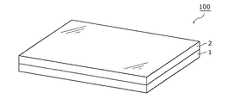
まず、本発明の一実施の形態に係る表示装置100の構成について、図1Aおよび図1Bを用いて説明する。図1Aおよび図1Bは、本発明の一実施の形態に係る表示装置100の概略構成を模式的に示す斜視図および断面図である。なお、図1Bは、ユーザの指がタッチパネル2に接触している状態を示している。 First, the structure of the
図1Aおよび図1Bに示すように、本発明の一実施の形態に係る表示装置100は、画像や文字等の情報を表示する表示領域(表示面)を有する表示パネル1と、当該表示パネル1の一主面側(表示面側)に対向して配置されるとともに表示パネル1への情報の入力などの各種操作を行うタッチパネル2とを備える。 As shown in FIGS. 1A and 1B, a
表示パネル1としては、例示すれば、液晶ディスプレイ(LCD)、プラズマディスプレイパネル(PDP)、有機ELディスプレイ(OLED)、無機ELディスプレイ、などを挙げることができる。 Examples of the
また、タッチパネル2は、ユーザの指やタッチペン等が接触する位置を検出する位置検出機能を有するとともに、検出した位置情報等の情報を表示パネルに入力する入力機能を有する。タッチパネル2は、さらに、文字情報等を書き込む書込入力機能を有しても良い。なお、タッチパネル2は、ユーザが表示パネル1に表示された情報を、当該タッチパネル2を介して視認することができるように構成されている。 The
タッチパネル2としては、例示すれば、ドットスペーサー方式、静電容量方式、または、抵抗膜方式等のタッチパネルを挙げることができる。なお、本実施の形態におけるタッチパネル2としては、静電容量方式を例にして説明するが、特にこれに限るものではない。 Examples of the
表示パネル1とタッチパネル2とは、後述する相対的な位置関係で、例えば光学透明粘着(OCA:Optical Clear Adhesive)テープと呼ばれる両面テープ(図示せず)を用いて貼り合わされている。 The
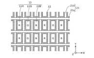
次に、本発明の一実施の形態に係る表示パネル1の構成について、図2Aおよび図2Bを用いて説明する。図2Aおよび図2Bは、図1Aに示した本発明の一実施の形態に係る表示装置100における表示パネル1の概略構成を模式的に示す平面図であり、表示領域(画像表示領域)の一部を拡大して示している。なお、図2Aは、本発明の一実施の形態に係る表示装置100における表示パネル1の第1の例であり、図2Bは、本発明の一実施の形態に係る表示装置100における表示パネル1の第2の例を示している。 Next, the configuration of the
表示パネル1は、行列状に配置された複数の画素によって構成された表示領域(画像表示領域)を有する。複数の画素の各々は、異なる色の複数のサブ画素(サブピクセル)を含む。各画素は同じ構成となっており、各画素において複数のサブ画素は画素の行方向または画素の列方向に沿って並んで配置されている。したがって、表示領域全体としては、異なる色のサブ画素が画素(サブ画素)の行方向または画素(サブ画素)の列方向に沿って一定のパターンで繰り返して配置されている。 The
図2Aおよび図2Bに示すように、本実施の形態における表示パネル1の1つの画素には、3つのサブ画素が含まれている。具体的には、赤色(R)に対応する赤色画素11R、緑色(G)に対応する緑色画素11G、および、青色(B)の対応する青色画素11Bが含まれている。赤色画素11R、緑色画素11Gおよび青色画素11Bは、画素の行方向(X軸方向)に沿って繰り返して配列されている。なお、画素の列方向(Y軸方向)には、同色のサブ画素が繰り返して配列されている。 As shown in FIGS. 2A and 2B, one pixel of
ここで、表示パネル1として、有機ELディスプレイを想定した場合、有機ELディスプレイは、ガラス基板上に形成された薄膜トランジスタを含む駆動回路層(平坦化層)上に、下部電極(アノード)と、上部電極(カソード)と、下部電極および上部電極の間に形成された有機発光層(発光部)と、有機発光層を区画する隔壁(バンク)と、上部電極の上に形成された封止樹脂層と、封止樹脂層の上に形成されたガラス基板とが配置された構成であり、赤色画素11R、緑色画素11Gおよび青色画素11Bは、各色の光を発する有機発光層に対応する。 Here, when an organic EL display is assumed as the
また、表示パネル1の表示領域は、複数の画素(サブ画素)からなる画素部と、隣り合う画素(サブ画素)の間の領域である非表示部とによって構成されている。画素部は、表示パネル1に表示される画像を構成する光が出射する部分であり、有機ELディスプレイでは発光領域である。非表示部は、表示領域のうち表示部以外の部分である。つまり、非表示部は、表示パネル1に表示される画像を構成する光が出射されない部分であり、有機ELディスプレイでは非発光領域である。 In addition, the display area of the
図2Aおよび図2Bに示すように、本実施の形態における画素部11は、赤色画素11R、緑色画素11Gおよび青色画素11Bの各サブ画素によって構成されている。一方、非表示部12は、画素間の領域、および/または、サブ画素(赤色画素11R、緑色画素11G、青色画素11B)間の領域であり、図2Aおよび図2Bに示すように、画素の行方向に延びる直線状の複数の行方向パターンと画素の列方向に延びる直線状の複数の列方向パターンとからなる。すなわち、非表示部12は、表示領域全体において格子状のパターン(格子パターン)として構成されている。 As shown in FIGS. 2A and 2B, the
ここで、非表示部12としては、例えば、各サブ画素間に対応するように形成されたブラックマトリクス(遮光部)とすることができる。ブラックマトリクスは、例えば表示パネル1の前面基板(タッチパネル側の基板)に形成されるカラーフィルタ層の一部である。カラーフィルタ層は、例えば、赤色用カラーフィルタ、緑色用カラーフィルタおよび青色用カラーフィルタの各色カラーフィルタと、各色カラーフィルタ間に形成されたブラックマトリクスとからなる。 Here, as the
また、非表示部12の別の例としては、例えば有機EL表示パネルにおける有機発光層を区画する隔壁(バンク)とすることもできる。なお、この隔壁は、例えば黒色の感光性材料によって形成することができ、隣り合う有機発光層の光が混色しないように隣りの有機発光層に進行する光を遮光する。 Moreover, as another example of the
また、図2Bでは、表示パネル1として、補助配線(バスバー)13を有する有機ELディスプレイを例示している。補助配線13は、全サブ画素に共通する上部電極(共通電極)と電気的に接続されており、例えば平坦化層上において下部電極と同層に形成されている。補助配線13は、表示画面の中央領域に生ずる上部電極の電圧降下を防止する機能を有する。 In FIG. 2B, an organic EL display having an auxiliary wiring (bus bar) 13 is illustrated as the
図2Bに示すように、本実施の形態における補助配線13は、画素の列方向(Y軸方向)に沿って延びるように複数本形成されている。また、補助配線13は、サブ画素ごとではなく、画素ごとに、画素の行方向において繰り返されるように形成されている。この場合、隔壁に対応する非表示部12のうち補助配線13が形成される部分(画素間領域)における非表示部12の幅は、補助配線13が形成されていない他の部分(一画素内のサブ画素間領域)における非表示部12の幅よりも広くなっている。すなわち、補助配線13は、幅の広い非表示部12(隔壁)に沿って形成されている。 As shown in FIG. 2B, a plurality of
次に、本実施の形態におけるタッチパネル2の構成について、図3Aおよび図3Bを用いて説明する。図3Aは、図1Aに示した本発明の一実施の形態に係る表示装置におけるタッチパネルの概略構成を模式的に示す断面図であり、図3Bは、図3Aに示すタッチパネルにおける電極パターンの構成を示す平面図である。なお、図3Aおよび図3Bに示すタッチパネル2は、多点検出を行うことが可能な投影型静電容量式のタッチパネルを、一例として挙げている。 Next, the structure of the
図3Aに示すように、タッチパネル2は、複数の第1電極線21aと複数の第2電極線21bとにより構成される電極パターン21と、第1電極線21aおよび第2電極線21bの間に形成される絶縁層22と、第1電極線21aが形成される第1基板23aと、第2電極線21bが形成される第2基板23bとを備える。 As shown in FIG. 3A, the
第1電極線21aと第2電極線21bとは、互いに短絡しないよう絶縁層22を間に介して離間して積層されており、電極パターン21は、平面視において(ユーザ側から見て)マトリクス状に形成されている。なお、本実施の形態において、第1基板23aをユーザ側の基板とする。絶縁層22としては、例えば透明樹脂によって構成することができる。また、第1基板23aおよび第2基板23bは、透光性を有する基材によって構成されており、例えばガラス基板または可撓性を有する透明樹脂からなるフレキシブル基板等の透明基板を用いることができる。 The
そして、電極パターン21(第1電極線21aおよび第2電極線21b)には所定の電圧が印加されており、ユーザの指がタッチパネル2の主面(本実施の形態では、第1基板23aの外表面)に接近または接触すると、ユーザの指と電極パターン21との間で容量結合が生じ、この接近により生じた電極線間の静電容量の変化に基づいて、ユーザの指が接触した接触位置を検出する。具体的には、指がタッチパネル2に近づくことにより隣り合う第1電極線21a間に起きる静電容量の変化を容量センサ用IC(図示せず)によって検知することで、X軸方向におけるユーザの指の接触位置を検出する。同様に、指が近づくことにより隣り合う第2電極線21b間に起きる静電容量の変化を容量検知用IC(図示せず)によって検知することで、Y軸方向におけるユーザの指の接触位置を検出する。このように、X軸方向およびY軸方向における各結合容量の変化を同時に検出することにより、ユーザがタッチパネル2にタッチした指の位置座標を検出することができる。なお、上述のタッチパネル2における接触位置の検出については、タッチパネルに係る公知・公用の技術を用いることが可能である。 A predetermined voltage is applied to the electrode pattern 21 (the
第1電極線21aは、第1電極パターンの一例であって、表示パネル1の画素の行方向(X軸方向)および画素の列方向(Y軸方向)のいずれか一方の方向(第1方向)に沿って形成される。図3Bに示すように、本実施の形態における第1電極線21aは、画素の行方向(X軸方向)に沿って延設された行電極線であって、画素の列方向において繰り返して複数本形成されている。 The
第2電極線21bは、第2電極パターンの一例であって、表示パネル1の画素の行方向(X軸方向)および画素の列方向(Y軸方向)のいずれか他方の方向(第2方向)に沿って形成される。図3Bに示すように、本実施の形態における第2電極線21bは、画素の行方向に沿って延設された列電極線であって、画素の行方向において繰り返して複数本形成されている。 The
ここで、各第1電極線21aおよび各第2電極線21bの少なくとも一部分は、金属である。各第1電極線21aおよび各第2電極線21bにおける金属部分の材料としては、抵抗率が小さくて導電性に優れ且つ屈曲性に優れたものを用いることが好ましい。このような材料としては、例えば、銅(Cu)、ニッケル(Ni)、アルミニウム(Al)、銀(Ag)およびクロム(Cr)から選ばれる少なくとも一種の金属またはその金属を含む合金の中から選ぶことができる。 Here, at least a part of each
このように、第1電極線21aおよび第2電極線21bの少なくとも一部に低抵抗の金属を用いることにより、第1電極線21aおよび第2電極線21bの配線全体をITO等の比較的高抵抗材料である透明導電性金属酸化物によって構成する場合と比べて、第1電極線21aおよび第2電極線21b(電極パターン21)を低抵抗化することができる。これにより、タッチパネルとしての座標位置検出精度を高めることができる。 Thus, by using a low-resistance metal for at least a part of the
本実施の形態では、各第1電極線21aおよび各第2電極線21bは、一定の線幅を有する線状の金属配線であり、配線全体が金属材料によって構成されている。これにより、電極パターン21の配線抵抗を小さくすることができる。 In the present embodiment, each
また、本実施の形態のように、電極パターン21に金属材料を用いることにより、曲げ応力に対する信頼性を向上させることができる。つまり、電極パターンをITO等で構成した場合では、タッチパネルの曲げによって、電極パターンが割れたり基板から剥離したりするといった問題が発生しやすい。一方、本実施の形態のように、電極パターン21を金属材料で構成することにより、タッチパネルを曲げたとしても、電極パターン21が割れたり基板から剥離したりすることを抑制できる。このように、本実施の形態における電極パターン21は、曲げ応力に対する信頼性が高い。 Moreover, the reliability with respect to a bending stress can be improved by using a metal material for the
なお、本実施の形態におけるタッチパネル2では、第1電極線21aおよび第2電極線21bを、対向する2つの透明基板(第1基板23a、第2基板23b)で挟むように構成したが、これに限らない。例えば、第1電極線21aと第2電極線21bとを絶縁した状態で全体を透明樹脂材料によって覆うように構成した透明導電フィルムを、タッチパネル2として用いても構わない。 In the
次に、本発明の一実施の形態に係る表示装置100における表示パネル1とタッチパネル2との相対的な位置関係について、図4Aおよび図4Bを用いて説明する。 Next, the relative positional relationship between the
図4Aおよび図4Bは、本発明の一実施の形態に係る表示装置の概略構成を示す平面図であり、表示パネルとタッチパネルとの相対的な位置関係を説明するための図である。なお、図4Aは、図2Aに示した第1の例の表示パネルに図3Bに示した電極パターンを有するタッチパネルを貼り合わせたときの状態を示しており、図4Bは、図2Bに示した本発明の第2の例の表示パネルに図3Bに示した電極パターンを有するタッチパネルを貼り合わせたときの状態を示している。 4A and 4B are plan views showing a schematic configuration of the display device according to the embodiment of the present invention, and are diagrams for explaining the relative positional relationship between the display panel and the touch panel. 4A shows a state where the touch panel having the electrode pattern shown in FIG. 3B is attached to the display panel of the first example shown in FIG. 2A, and FIG. 4B shows the state shown in FIG. 2B. The state when the touch panel which has the electrode pattern shown to FIG. 3B on the display panel of the 2nd example of this invention was bonded together is shown.
本実施の形態における表示装置100は、図4Aおよび図4Bに示すように、平面視したときに(Z軸方向から見たときに)、タッチパネル2における電極パターン21(第1電極線21aおよび第2電極線21b)の金属の部分が表示パネル1の非表示部12内に存在するように構成されている。つまり、電極パターン21(第1電極線21aおよび第2電極線21b)の金属の部分が非表示部12と重なるように構成されており、電極パターン21の金属の部分が非表示部12に隠れるように配置されている。 As shown in FIGS. 4A and 4B,
図4Aでは、電極パターン21が非表示部12のパターンと一致するように、且つ、電極パターン21の線幅が非表示部12の線幅よりも狭くなるように構成されている。より具体的には、第1電極線21aおよび第2電極線21bは、非表示部12における行方向および列方向の全ての方向の線と重なるように形成されており、かつ、非表示部12から画素部11にはみ出さないように形成されている。 In FIG. 4A, the
また、図4Aでは、電極パターン21が非表示部12の行方向パターンおよび列方向パターンの全てに対応するように構成しているが、図4Bに示すように、第2電極線21bについては、非表示部12の列方向パターンに対して数本置きに間引いて配設してもよい。 4A, the
具体的には、複数の第1電極線21aの各々は、画素の列方向(X軸方向)において隣り合うサブ画素の間に配置されている。つまり、第1電極線21aは、サブ画素に対して間引かすに配置されている。一方、複数の第2電極線21bの各々は、画素の行方向(Y軸方向)において隣り合う画素の間に配置されている。つまり、第2電極線21bは、サブ画素に対して間引いて配置されている。 Specifically, each of the plurality of
この場合、図4Bに示すように、第2電極線21bは、補助配線13の上方に形成することが好ましい。すなわち、第2電極線21bは、補助配線13が形成されている非表示部12内に形成されることが好ましい。また、補助配線13がX軸方向に沿って形成されている場合には、X軸方向に延設される第1電極線21aを補助配線13の上方に形成することが好ましい。また、補助配線13がX軸方向およびY軸方向の両方に沿って形成されている場合には、第1電極線21aおよび第2電極線21bの両方を補助配線13の上方に形成することが好ましい。 In this case, as shown in FIG. 4B, the
なお、図4Bでは、第2電極線21bを間引いた構成としたが、第1電極線21aを間引いた構成とすることもできる。また、第1電極線21aおよび第2電極線21bの両方を間引いた構成とすることもできる。 In FIG. 4B, the
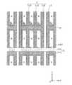
次に、図4Bに示す本発明の一実施の形態に係る表示装置の詳細構成について、図5、図6Aおよび図6Bを用いて説明する。図5は、本発明の一実施の形態に係る表示装置の平面図であり、表示パネルとタッチパネルとの相対的な位置関係を示している。図6Aは、図5のX−X’線における本発明の一実施の形態に係る表示装置の断面図である。図6Bは、図5のY−Y’線における本発明の一実施の形態に係る表示装置の断面図である。なお、図5に示す表示装置は、図4Bに示す表示装置と同様に、表示パネル1として補助配線を有する有機ELディスプレイを用い、また、タッチパネル2として静電容量方式のものを用いた例を示しているが、これに限定される訳ではない。 Next, a detailed configuration of the display device according to the embodiment of the present invention illustrated in FIG. 4B will be described with reference to FIGS. 5, 6A, and 6B. FIG. 5 is a plan view of the display device according to the embodiment of the present invention, and shows the relative positional relationship between the display panel and the touch panel. 6A is a cross-sectional view of the display device according to the embodiment of the present invention taken along line X-X ′ of FIG. 5. 6B is a cross-sectional view of the display device according to the embodiment of the present invention taken along line Y-Y ′ of FIG. 5. The display device shown in FIG. 5 is an example in which an organic EL display having an auxiliary wiring is used as the
図5に示すように、有機ELディスプレイである表示パネル1は、上述のように、各々が、赤色画素11R、緑色画素11Gおよび青色画素11Bの3つのサブ画素を含む複数の画素からなる画素部(発光領域)11と、画素部11以外の領域である非表示部(非発光領域)12とからなる表示領域を有する。 As shown in FIG. 5, the
また、図6Aおよび図6Bに示すように、表示パネル1は、ガラス基板14と、ガラス基板14上に形成された駆動トランジスタ15等の薄膜トランジスタを含む画素回路と、画素回路等を平坦化するための平坦化層16とからなるアクティブマトリクス基板を備える。また、表示パネル1は、各サブ画素に対応するようにして形成された有機EL素子17を備える。有機EL素子17は、平坦化層16上に形成された下部電極(アノード)17AMと、下部電極17AM上に形成された有機発光層17ELと、有機発光層17EL上に形成された上部電極(カソード)17Kとを備える。さらに、表示パネル1は、各有機発光層17ELを区画する隔壁(バンク)17BNKと、上部電極17Kの上に形成された封止樹脂層18と、封止樹脂層18の上に形成されたガラス基板(対向基板)19とを備える。赤色画素11R、緑色画素11Gおよび青色画素11Bは、各色の光を発する有機発光層17ELに対応する。 Further, as shown in FIGS. 6A and 6B, the
なお、隔壁17BNKはピクセルバンクとしているが、これに限らない。また、本実施の形態において、非表示部12は隔壁17BNKであるが、ブラックマトリクス(遮光部)を非表示部12としてもよい。 The partition wall 17BNK is a pixel bank, but is not limited thereto. In the present embodiment, the
また、図5および図6Aに示すように、隣り合う画素間には上部電極17Kと電気的に接続された補助配線(バスバー)13が形成されている。具体的に、補助配線13は、一の画素における青色画素11B(サブ画素)と他の画素における赤色画素11R(サブ画素)との間に配置されており、画素の列方向(Y軸方向)に沿って直線状に複数本延設されている。ここで、補助配線13は、表示領域中央部における電圧降下を抑制するために、全サブ画素に共通する上部電極17Kと電気的に接続されている。本実施の形態では、Y軸方向に沿って隔壁17BNKに形成された直線状の開口を介して、補助配線13と上部電極17Kとが電気的に接続されている。 As shown in FIGS. 5 and 6A, an auxiliary wiring (bus bar) 13 that is electrically connected to the
赤色画素11R、緑色画素11Gおよび青色画素11Bの各サブ画素には、当該サブ画素を駆動するための駆動トランジスタ15と、複数のサブ画素の中から発光させる画素を選択するための選択トランジスタ(不図示)とが含まれている。図6Bに示すように、駆動トランジスタ15は、例えばボトムゲート型の薄膜トランジスタであって、ガラス基板14の上に形成されたゲート電極15Gと、ゲート電極15Gの上に形成されたゲート絶縁膜15GIと、ゲート絶縁膜15GIの上に形成された半導体層(チャネル層)15SCと、半導体層15SCの上に形成されたチャネルエッチングストッパ層15CESと、半導体層15SCの両端の上に形成された一対のソース電極15Sおよびドレイン電極15Dとを備える。なお、半導体層15SCとしては、シリコン半導体または酸化物半導体等を用いることができる。 The sub-pixels of the
本実施の形態における駆動トランジスタ15は、n型TFTであるので、図6Bに示すように、平坦化層16に形成されたコンタクトホール16CHを介して、駆動トランジスタ15のドレイン電極15Dと下部電極17AMとが電気的に接続されている。図示しないが、駆動トランジスタ15のソース電極15Sは、電源線(不図示)に接続される。なお、駆動トランジスタ15がp型の場合、コンタクトホール16CHを介して駆動トランジスタ15のソース電極15Sが下部電極17AMと接続される。 Since the driving
図6Aおよび図6Bに示すように、タッチパネル2は、画素の行方向(X軸方向)に沿って第1電極線21aが形成された第1基板23aと、画素の列方向(Y軸方向)に沿って第2電極線21bが形成された第2基板23bとが、絶縁層(不図示)を介して貼り合せられて構成されている。第1電極線21aおよび第2電極線21bは、全体が金属によって構成された直線状の金属細線であり、線幅は一定である。また、図示しないが、本実施の形態では、第1電極線21aおよび第2電極線21bは、横長矩形状の検出領域(検出面)の全体にわたって形成されているので、第1電極線21aの配線長は第2電極線21bの配線長よりも長くなっている。 6A and 6B, the
図5に示すように、タッチパネル2における第2電極線(金属配線)21bは、平面視において、表示パネル1における補助配線13と重なるように位置合わせされており、サブ画素間には配置されていない。また、タッチパネル2における第1電極線(金属配線)21aは、平面視において、各サブ画素に対応して設けられたコンタクトホール16CHの上に位置合わせされている。つまり、第1電極線21aは、コンタクトホール16CHに重ねて配置されている。なお、本実施の形態において、第2電極線21bの線幅が補助配線13の線幅よりも小さくなるように構成されているが、第2電極線21bの線幅は補助配線13の線幅よりも大きくても構わない。 As shown in FIG. 5, the second electrode line (metal wiring) 21b in the
さらに、図6Aおよび図6Bに示すように、非表示部(非発光領域)12においてX軸方向に隣り合うサブ画素間の幅をW1とし、第1電極線21aの幅(線幅)をW2とし、非表示部(非発光領域)12においてY軸方向に隣り合うサブ画素間の幅をW3とし、第2電極線21bの幅(線幅)をW4とすると、W1−W2≦W3−W4の関係を満たすことが好ましい。なお、本実施の形態において、補助配線13は画素間に配置されているので、幅W1は画素間の幅としている。 Further, as shown in FIGS. 6A and 6B, the width between the sub-pixels adjacent in the X-axis direction in the non-display portion (non-light emitting region) 12 is W1, and the width (line width) of the
以下、本実施の形態に係る表示装置において、上記構成とすることの好ましい理由について説明する。 Hereinafter, the reason why the above-described configuration is preferable in the display device according to the present embodiment will be described.
まず、本実施の形態において、第2電極線21bが補助配線13上にのみに存在させることが好ましい理由について説明する。 First, the reason why the
第2電極線21bは、画素間だけではなく、一画素内のサブ画素間に配置することも考えられる。しかしながら、一画素内のサブ画素間は画素間に比べて非表示部12の幅(間隔)が狭いことから、第2電極線21bを画素部(発光領域)11にかからないように配置するには第2電極線21bを細くしなければならない。このため、補助配線13が形成される画素間には太い第2電極線(金属配線)21bが配置され、一画素内のサブ画素間には細い第2電極線(金属配線)21bが配置されることになる。 The
ここで、静電容量方式のタッチパネル2において、第1電極線21aおよび第2電極線21bによる検知感度は、配線抵抗と配線容量との積で表される時定数が小さければ小さいほど良くなる。 Here, in the
したがって、上記のように、補助配線13が形成される画素間に太い第2電極線(金属配線)21bを配置し、一画素内のサブ画素間に細い第2電極線(金属配線)21bを配置すると、一画素内のサブ画素間に形成された第2電極線21bは、画素間に形成された第2電極線21bと比べて、検知感度が著しく小さくなってしまう。つまり、この場合、一画素内のサブ画素間に形成された細い第2電極線21bは、位置検出を算出するときに使われず、無意味なものになる。 Therefore, as described above, the thick second electrode line (metal wiring) 21b is arranged between the pixels where the
このことから、タッチパネル2の第2電極線21bは、補助配線13上のみに配置することが好ましい。これにより、形成した第2電極線21bを無駄にすることなく、位置検出のために効率よく利用することができる。 For this reason, the
次に、第1電極線21aをコンタクトホール16CH上に配置することが好ましい理由について説明する。 Next, the reason why the
タッチパネル2において、X軸方向の検知感度とY軸方向の検知感度とを同等にするには、X軸方向に沿って形成される第1電極線21aの配線抵抗とY軸方向に沿って形成される第2電極線21bの配線抵抗とを同等にすればよい。つまり、配線抵抗が同じになるように、第1電極線21aの長さ(配線長)と第2電極線21bの長さ(配線長)とに応じて、第1電極線21aの幅(配線幅)と第2電極線21bの幅(配線幅)とを所望に設定すればよい。具体的には、第1電極線21aの幅(W2)と第2電極線21bの幅(W4)との関係に関しては、配線長がより長い方の電極線の幅を太くすることで、X軸方向とY軸方向との検知感度をより同等にすることが可能となる。 In the
具体的には、第1電極線21aの長さをL1とし、第2電極線21bの長さをL2とすると、L1>L2の場合にはW2>W4の関係を満たすように構成し、L1<L2の場合にはW2<W4の関係を満たすように構成すればよい。 Specifically, assuming that the length of the
この関係を満たすように第1電極線21aおよび第2電極線21bを構成することにより、第1電極線21aの長さと第2電極線21bの長さが異なる場合であっても、第1電極線21aの配線抵抗と第2電極線の配線抵抗との差を小さくすることができる。これにより、タッチパネル2において、X軸方向における検知感度とY軸方向における検知感度との感度差を小さくすることができる。 By configuring the
例えば、タッチパネル2の検出面(検出領域)の形状が横長矩形である場合、電極線の取り出し構造をX軸方向およびY軸方向のいずれにおいても片側取り出しとすると、長辺方向(X軸方向)に延設される第1電極線21aの方が、短辺方向(Y軸方向)に延設される第2電極線21bよりも配線長が長くなっている(L1>L2)。この場合、第1電極線21aおよび第2電極線21bの配線抵抗を同等にするには、第1電極線21aの幅(W2)を第2電極線21bの幅(W4)よりも大きくすればよい(W2>W4)。 For example, when the shape of the detection surface (detection region) of the
ここで、各サブ画素に対応して設けられたコンタクトホール16CHは、非表示部(非発光領域)12である隔壁17BNKの下に形成されている。したがって、第1電極線21aをコンタクトホール16CHに重ねて配置することにより、第1電極線21aの線幅を容易に広げることが可能となる。 Here, the contact hole 16CH provided corresponding to each sub-pixel is formed under the partition wall 17BNK which is the non-display portion (non-light emitting region) 12. Accordingly, by arranging the
このことから、第1電極線21aは、コンタクトホール16CH上に配置することが好ましい。つまり、第1電極線21aをコンタクトホール16CHに重ねて配置することにより、第1電極線21aの配線長が第2電極線21bの配線長よりも長い場合であっても、第1電極線21aの線幅を容易に太くすることできる。これにより、第1電極線21aの検知感度と第2電極線21bの検知感度との差(感度差)を小さくすることができる。 Therefore, it is preferable that the
なお、タッチパネル2を大型化すると、極線の配線長が長くなって高抵抗化するので、電極線の配線抵抗値を下げるために、電極線の取り出し構造を両側取り出しにして、1本の電極線の長さを短くすることが考えられる。例えば、タッチパネル2の検出面(検出領域)の形状が横長矩形である場合、検出面の左右の両短辺から電極線を取り出すことが考えられる。この場合、長辺方向(X軸方向)に延設される第1電極線21aを、片側取り出しの場合と比べて、約1/2の長さにすることができきる。このような場合でも、第1電極線21aの配線長と第2電極線21bの配線長とを比較して、長い方の電極線の配線幅を太くすることが望ましい。例えば、両側取り出し構造にした結果、短辺方向(Y軸方向)に延設される第2電極線21bの方が、長辺方向(X軸方向)に延設される第1電極線21aよりも配線長が長くなった場合(L2>L1)、第1電極線21aおよび第2電極線21bの配線抵抗を同等にするには、第2電極線21bの幅(W4)を第1電極線21aの幅(W2)よりも大きくすればよい(W4>W2)。 In addition, when the
また、表示パネル1におけるコンタクトホール16CHの位置は、図5に示される位置に限られず、図7に示すような位置としても構わない。図7に示すように、コンタクトホール16CHをサブ画素の隅にずらすことによって、赤色画素11R、緑色画素11Gおよび青色画素11Bの領域(発光領域)の面積を大きくすることができる。 Further, the position of the contact hole 16CH in the
次に、X軸方向において隣り合うサブ画素間の幅(W1)と、第1電極線21aの線幅(W2)と、Y軸方向において隣り合うサブ画素間の幅(W3)と、第2電極線21bの線幅(W4)とが、W1−W2≦W3−W4の関係式を満たすことが好ましい理由について説明する。 Next, the width (W1) between the sub-pixels adjacent in the X-axis direction, the line width (W2) of the
例えば、表示パネル1とタッチパネル2とのアライメントがずれたこと等によって、第2電極線21bの位置が図5において左右にずれて画素部11にかかってしまった場合、赤色画素11R、緑色画素11Gおよび青色画素11Bのいずれかの単色光が第2電極線21bによって遮光されてしまう。そのため、RGBの輝度バランス(ホワイトバランス)が崩れるため、画質の低下が顕著となる。 For example, when the position of the
一方、同様にアライメントのずれ等によって、第1電極線21aの位置が図5において上下にずれた場合、赤色画素11R、緑色画素11Gおよび青色画素11Bを同程度に遮光することになるので、輝度は低下するものの輝度バランス(ホワイトバランス)の崩れは小さく、画質の低下も限定的である。 On the other hand, when the position of the
ここで、X軸方向における第1電極線21aの位置ずれによるマージンは、X軸方向の隣接サブ画素間の幅(W1)と第1電極線21aの幅(W2)との差(W1−W2)として表される。また、Y軸方向における第2電極線21bの位置ずれによるマージンは、Y軸方向の隣接サブ画素間の幅(W3)と第2電極線21bの幅(W4)との差(W3−W4)で表される。したがって、アライメントのずれ等による画質への影響を考慮すると、上述のとおり、X軸方向の位置ずれのマージンはY軸方向の位置ずれのマージンよりも小さいことが好ましく、W1−W2≦W3−W4の関係式を満たすことが望ましい。 Here, the margin due to the positional deviation of the
この関係式を満たすことにより、表示パネル1とタッチパネル2とのアライメントのずれが発生したとしても、輝度バランスの崩れを抑制することができる。これにより、画素の視認性が低下することを抑制することができる。 By satisfying this relational expression, even if an alignment shift between the
以上説明したように、本実施の形態に係る表示装置100によれば、表示パネル1とタッチパネル2とは、タッチパネル2の電極パターン21の金属部分が表示パネル1の非表示部12の線幅内で重なるように位置合わせがなされて貼り合わされている。 As described above, according to
すなわち、本実施の形態では、タッチパネル2の電極パターン21(第1電極線21aおよび第2電極線21b)を構成する材料として、光透過性を気にすることなく、導電性に優れた低抵抗の金属材料を用い、第1電極線21aおよび第2電極線21bを金属配線としている。これにより、透明電極材料のみで第1電極線21aおよび第2電極線21bを構成する場合と比べて、第1電極線21aおよび第2電極線21bの配線抵抗を小さくすることができる。したがって、容易にタッチパネル2を大画面化および高精細化することができる。 That is, in this embodiment, the material constituting the electrode pattern 21 (the
その上で、さらに、第1電極線21aおよび第2電極線21bが表示パネル1の非表示部12内において非表示部12と重なるようにすることで、第1電極線21aおよび第2電極線21bによって表示パネル1の画像が遮光されてしまうことを抑制することができる。すなわち、第1電極線21aの線幅(W2)は非表示部12のY軸方向における幅よりも小さく、かつ、第2電極線21bの線幅(W4)は非表示部12のX軸方向における幅よりも小さくなっている。これにより、画像の視認性が低下することを抑制することができる。 In addition, the
さらに、第1電極線21aおよび第2電極線21bを金属配線とすることによって、タッチパネル2を曲げたとしても、第1電極線21aおよび第2電極線21bが割れたり第1基板23aおよび第2基板23bから剥離したりすることを抑制することができる。これにより、曲げ応力に対する信頼性を向上させることができる。 Further, by using the
このように、本実施の形態に係る表示装置100によれば、表示パネル1の画像表示の視認性を妨げることなく、タッチパネル2の電極パターン21の導電性を確保できる。これにより、比較的大インチサイズ、高精細および良視認性のタッチパネル付き表示装置を実現することができる。 Thus, according to the
例えば、電極パターン21(第1電極線21aおよび第2電極線21b)をAg等の低抵抗金属によって構成することで、電極パターン21を数十μmオーダの線幅である非表示部12内に形成したとしても、高精度の座標位置検出精度を有するタッチパネルを実現することができる。また、Ag等の金属からなる電極パターン21は不透光であって遮光性を有するが、電極パターン21(第1電極線21aおよび第2電極線21b)は、表示パネル1の非表示部12内に隠れるように形成されるので、表示パネル1の画像表示の視認性は低下しない。その結果、画面の大型化や解像度の高精細化に対応可能なタッチパネル付き表示装置を実現することができる。 For example, the electrode pattern 21 (the
また、本実施の形態において、タッチパネル2の電極パターン21の配設パターンは、図4Bに示すように、数本置きに間引いたものであっても良い。現在のアイコンタッチ入力の用途におけるタッチパネルには表示パネルほどの高精細は要求されていないので、電極パターン21を上述のように間引いた構成としても指の座標位置検出精度を維持することができる。したがって、電極パターン21を間引いた構成とすることにより、電極パターン21の各電極線に対応する容量検知用ICを削減することができるので、コスト削減および重量低減といった効果を得ることができる。 Further, in the present embodiment, the arrangement pattern of the
また、本実施の形態において、タッチパネル2の電極パターン21の線幅は、その形成の際の形状精度、位置精度、およびタッチパネル2と表示パネル1との貼り合わせ精度、などを考慮した上で、表示パネル1の非表示部12の線幅からはみ出さないことを上限に、できるだけ幅太にする方が、導電性の観点からは望ましい。これにより、電極パターン21を一層低抵抗化することができるので、指の座標位置の検出精度をさらに向上させることができる。なお、非表示部12の線幅が数十μmオーダの20インチ程度の表示パネルに対応するタッチパネルにおいては、電極パターン21の線幅は5〜7μm程度であっても、指の座標位置を高精度に検出することができる。 Further, in the present embodiment, the line width of the
また、本実施の形態において、第1電極線21aおよび第2電極線21bをいずれもストレート(直線)形状として、電極パターン21の平面視形状が図3Bに示すようなメッシュパターン(格子パターン)となるように構成したが、例えば図8に示すような形状の電極パターンとすることもできる。図8は、本発明の一実施の形態に係る表示装置のタッチパネルにおける第1変形例の電極パターンの構成を示す平面図である。 In the present embodiment, the
図8に示すように、本変形例における第1電極線21aおよび第2電極線21bは、平面視形状が波型形状または蛇行形状となるように構成されており、電極パターン21が波線パターンとなっている。但し、この場合においても、電極パターン21は、非表示部12内に形成し、電極パターン21が非表示部12から画素部11にはみ出さないように構成する。 As shown in FIG. 8, the
このように、電極パターン21の平面視形状を波型形状または蛇行形状とすることにより、高精細化のために電極線幅を太くできないような場合であっても、指で触れた際の容量を大きくすることができるので、容量変化の検知感度を向上させることできる。さらに、電極パターン21の平面視形状を波型形状または蛇行形状とすることで、表示装置(タッチパネル)を曲げた際における電極パターン21の断線や剥離を抑制することができ、電極パターン21の機械的強度を向上させることができるといった効果を得ることもできる。 As described above, the
なお、本変形例では、第1電極線21aおよび第2電極線21bの両方とも波型形状としているが、第1電極線21aおよび第2電極線21bのどちらか一方のみを波型形状としても構わない。 In this modification, both the
また、本実施の形態における電極パターン21の形状としては、図9Aおよび図9Bに示すようなパターンとしてもよい。図9Aおよび図9Bは、それぞれ、本発明の一実施の形態に係る表示装置のタッチパネルにおける電極パターン(Y軸方向)の第2変形例および第3変形例の構成を示す平面図である。 The shape of the
図9Aに示すように、第2変形例では、電極パターン60Aを構成するY軸方向に延設される1本の第2電極パターン61Aは、各々の角部同士が接続されるとともにY軸方向に複数個配列されたダイヤマークをなす矩形状の透明電極パターン(電極パッド)61aと、各透明電極パターン61aの中央を通るように透明電極パターン61aに積層された金属線62とによって構成されている。金属線62は、第2電極パターン61Aにおける金属の部分であって、低抵抗金属細線である。 As shown in FIG. 9A, in the second modification, one
また、図9Bに示すように、第3変形例における電極パターン60BのY軸方向の1本の第2電極パターン61Bは、Y軸方向に複数個配列されたダイヤマークをなす矩形状の透明電極パターン61a(電極パッド)と、各々の透明電極パターン61aの角部同士を接続する金属線63とによって構成されている。金属線62は、第2電極パターン61Bにおける金属の部分であって、透明電極パターン61aの繋ぎ目部分に配設された低抵抗金属細線である。 Further, as shown in FIG. 9B, one
図9Aおよび図9Bにおいて、金属線62、63は、図4Aまたは図4Bに示す電極パターン21と同様に、表示パネル1の非表示部12の線幅内において非表示部12と重なるように形成されている。 9A and 9B, the
金属線62、63の材料としては、電極パターン21と同様に、銅(Cu)、ニッケル(Ni)、アルミニウム(Al)、銀(Ag)およびクロム(Cr)から選ばれる少なくとも一種の金属またはその金属を含む合金の中から選ぶことができる。また、透明電極パターン61aの材料としては、ITOまたはインジウム亜鉛酸化物(IZO:Indium Zinc Oxide)等の透明導電性金属酸化物を用いることができる。 As the material of the
なお、図9Aおよび図9Bでは、Y軸方向に延設される1本の第2電極パターンについて説明したが、実際には、これを複数本、平行に配列してタッチパネルの電極パターンを構成する。また、図9Aおよび図9Bでは、Y軸方向に延設される第2電極パターンについて説明したが、X軸方向に延設される第1電極パターンについてもそれぞれ同様の構成とすることができる。この場合、X軸方向およびY軸方向の各電極パターンの透明電極パターン61aが重ならないように、タッチ面が透明電極パターン61aによって敷き詰められるように構成される。 9A and 9B, one second electrode pattern extending in the Y-axis direction has been described, but actually, a plurality of these patterns are arranged in parallel to constitute the electrode pattern of the touch panel. . 9A and 9B, the second electrode pattern extending in the Y-axis direction has been described, but the first electrode pattern extending in the X-axis direction can have the same configuration. In this case, the touch surface is configured to be covered with the
このように、図9Aおよび図9Bに示す変形例に係る電極パターン60A、60Bによれば、金属線62、63が表示パネル1の非表示部12内に形成されているので、図4Aまたは図4Bに示す電極パターン21と同様に、表示パネル1の画像表示の視認性を低下させることなく、電極線を低抵抗化することができる。これにより、画面の大型化や解像度の高精細化に対応可能なタッチパネル付き表示装置を実現することができる。 As described above, according to the
さらに、図9Aおよび図9Bに示す変形例における電極パターン60A、60Bは、面積の大きい透明電極パターン61aを有するので、容量変化の検知感度を向上させることができる。 Furthermore, since the
なお、図9Bのように金属線63を透明電極パターン61aの繋ぎ目のみに部分線として配設するよりも、図9Aのように金属線62を透明電極パターン61aの中を通って連続線として配設する方が、電極パターンとしては導電性に優れ、より低抵抗化することができる。但し、図9Aの電極パターン60Aまたは図6Bの電極パターン60Bのどちらの形態を採用するかは、表示装置に要求される性能に応じて適宜選択すればよい。 In addition, as shown in FIG. 9B, rather than arranging the
また、本実施の形態のように、表示パネル1の平面視形状は、正方形ではなく長方形であることが多い。この場合、タッチパネル2の電極パターン21では、X軸方向に配設された複数の第1電極線21aとY軸方向に配設された複数の第2電極線21bとの長さが異なる。そこで、第1電極線21aの長さと第2電極線21bの長さとが異なっていても、上述のとおり、X軸方向とY軸方向とで各電極線の配線抵抗(電気抵抗値)が略一致するように、例えば、長さが長い方の電極線の線幅を長さの短い方の電極線の線幅より幅太にすることが好ましい。 Further, as in the present embodiment, the planar view shape of the
また、図4Bに示すように、第2電極線21bを補助配線13の上方に形成したが、第2電極線21bを非表示部12と重畳する位置に形成された他の配線の上方に形成しても構わない。例えば、第2電極線21b(または第1電極線21a)を、隔壁と重なる位置に形成するとともに、有機EL素子を駆動する薄膜トランジスタ(駆動トランジスタ)に電源を供給する電源線の上方に形成しても構わない。 Further, as shown in FIG. 4B, the
また、本実施の形態において、第1電極線21aおよび第2電極線21bに重畳させる非表示部12は、表示パネル1における隔壁17BNKとしたが、表示パネル1におけるブラックマトリクスを非表示部12としても構わない。これにより、金属配線である第1電極線21aおよび第2電極線21bがブラックマトリクスによって覆われるので、第1電極線21aおよび第2電極線21bによって表示パネル1の画像の視認性が低下することを抑制することができる。 Further, in the present embodiment, the
次に、本発明の実施の形態に係る表示装置の実施例と比較例に係る表示装置とについて説明する。 Next, examples of display devices according to embodiments of the present invention and display devices according to comparative examples will be described.
本実施例では、20inchサイズの表示パネル1とタッチパネル2とにおいて、非表示部12であるブラックマトリクス(BM)と重なる位置にAgからなる電極パターン21を配設した。また、比較例では、20inchサイズの表示パネルとタッチパネルとにおいて、非表示部であるブラックマトリクス(BM)と重なる位置にITOからなる電極パターンを配設した。なお、タッチパネルの基板(第1基板、第2基板)の大きさは、縦が270mmで、横が460mmのものを用いた。本実施例と比較例とは、電極パターンのみが異なり、本実施例におけるAgからなる電極パターン21は、厚みが5μm程度で、線幅が5μmのストレート形状であり、比較例におけるITOからなる電極パターン21は、厚みが100nmで、線幅が30μmのストレート形状である。 In the present embodiment, the
このように構成された本実施例と比較例とについて、タッチパネルにおける位置検出の感度を測定すると、Agからなる電極パターンである本実施例では実用上十分な感度が得られたが、ITOからなる電極パターンである比較例では、厚膜化および幅広化しているにもかかわらず、十分な感度を得ることができなかった。 When the sensitivity of the position detection on the touch panel was measured for this example and the comparative example configured as described above, practically sufficient sensitivity was obtained in this example, which is an electrode pattern made of Ag, but made of ITO. In the comparative example, which is an electrode pattern, sufficient sensitivity could not be obtained despite the increase in thickness and width.
このように感度が異なる原因は、電極パターンの材料であるAgとITOとの電気導電性の違いによるものと考えられる。この場合、ITOの電極パターンの膜厚をさらに厚くし低抵抗化することも考えられるが、その場合にはITO成膜時における剥離の問題が懸念される。また、ITOの電極パターンを厚膜化すると、表示装置をフレキシブルディスプレイとして用いる場合において電極パターンの剥離の問題がさらに顕著になることに加えて、表示パネルが屈曲した場合において電極パターンに割れが生じるという問題もある。したがって、ITOの電極パターンを低抵抗化する手段として単純に厚膜化することを採用することができない。一方、Agからなる電極パターンは、抵抗率が低く導電性に優れているので、厚膜化することなく低抵抗配線を容易に実現することができる。 The cause of the difference in sensitivity is considered to be due to the difference in electrical conductivity between Ag, which is the material of the electrode pattern, and ITO. In this case, it may be possible to further reduce the resistance by further increasing the thickness of the ITO electrode pattern. In addition, when the electrode pattern of ITO is thickened, the problem of peeling of the electrode pattern becomes more noticeable when the display device is used as a flexible display, and the electrode pattern is cracked when the display panel is bent. There is also a problem. Therefore, it is not possible to simply increase the thickness of the ITO electrode pattern as a means for reducing the resistance. On the other hand, since the electrode pattern made of Ag has low resistivity and excellent conductivity, low resistance wiring can be easily realized without increasing the thickness.
また、他の実施例として、上記の本実施例におけるAgからなる電極パターンの形状を、ストレート形状ではなく、蛇行した形状に形成することができる。このような態様にすることで、タッチパネルの位置検出の感度がさらに向上することを確認した。なお、これは、指との接触面積が増加した効果によるものと考えられる。 As another embodiment, the shape of the electrode pattern made of Ag in the above-described embodiment can be formed in a meandering shape instead of a straight shape. It was confirmed that the sensitivity for detecting the position of the touch panel was further improved by adopting such an embodiment. This is thought to be due to the effect of increasing the contact area with the finger.
以上、本発明に係る表示装置について、実施の形態および変形例に基づいて説明したが、本発明は、上記の実施の形態および変形例に限定されるものではない。例えば、各実施の形態および変形例に対して当業者が思いつく各種変形を施して得られる形態や、本発明の趣旨を逸脱しない範囲で各実施の形態および変形例における構成要素および機能を任意に組み合わせることで実現される形態も本発明に含まれる。なお、本発明は、表示装置としてだけではなく、表示装置に貼り合わされる前のタッチパネルとしても適用することができる。 While the display device according to the present invention has been described based on the embodiments and the modifications, the present invention is not limited to the above-described embodiments and modifications. For example, the form obtained by making various modifications conceived by those skilled in the art with respect to each embodiment and modification, and the components and functions in each embodiment and modification are arbitrarily set within the scope of the present invention. Forms realized by combining them are also included in the present invention. Note that the present invention can be applied not only as a display device but also as a touch panel before being attached to the display device.
本発明は、タッチパネルを備える各種電子機器において広く利用することができ、電子機器の操作に用いられるタッチパネルおよびタッチパネルを備えた表示装置等において有用である。 The present invention can be widely used in various electronic devices including a touch panel, and is useful in a touch panel used for operation of the electronic device, a display device including the touch panel, and the like.
1 表示パネル
2 タッチパネル
11 画素部
11R 赤色画素(サブ画素)
11G 緑色画素(サブ画素)
11B 青色画素(サブ画素)
12 非表示部
13 補助配線
14、19 ガラス基板
15 駆動トランジスタ
15G ゲート電極
15GI ゲート絶縁膜
15SC 半導体層
15CES チャネルエッチングストッパ層
15S ソース電極
15D ドレイン電極
16 平坦化層
16CH コンタクトホール
17 有機EL素子
17AM 下部電極
17EL 有機発光層
17K 上部電極
17BNK 隔壁
18 封止樹脂層
21、60A、60B 電極パターン
21a 第1電極線
21b 第2電極線
22 絶縁層
23a 第1基板
23b 第2基板
61A、61B 第2電極パターン
61a 透明電極パターン
62、63 金属線
100 表示装置DESCRIPTION OF
11G green pixel (sub pixel)
11B Blue pixel (sub pixel)
DESCRIPTION OF
Claims (11)
Translated fromJapanese前記表示パネルに対向するタッチパネルと、を備え、
前記表示パネルは、
隣り合う画素の間の領域である非表示部を有し、
前記タッチパネルは、
前記画素の行方向および前記画素の列方向のいずれか一方である第1方向に沿って形成され、少なくとも一部分が金属である複数の第1電極パターンと、
前記画素の行方向および前記画素の列方向のいずれか他方である第2方向に沿って形成され、少なくとも一部分が金属である複数の第2電極パターンとを有し、
前記複数の第1電極パターンおよび前記複数の第2電極パターンの前記金属の部分は、平面視において、前記表示パネルの前記非表示部内に存在し、
前記複数の画素の各々は、前記第1方向に沿って配置された異なる色の複数のサブ画素を含み、
前記複数のサブ画素の各々は、上部電極と、下部電極と、前記上部電極および前記下部電極の間に形成されるとともに当該画素に対応して形成された有機発光層とを含み、
前記表示パネルは、前記有機発光層を区画するとともに前記非表示部に対応して形成された隔壁と、前記隔壁に覆われるように形成されるとともに前記上部電極と電気的に接続された補助配線とを有し、
前記複数のサブ画素の各々は、当該サブ画素を駆動するためのトランジスタを有し、
前記トランジスタのソース電極またはドレイン電極と前記下部電極とは、コンタクトホールにより接続され、
平面視において、前記コンタクトホールは、前記非表示部と重なる位置に形成され、
前記複数の第1電極パターンの各々は、前記第2方向において隣り合う前記サブ画素の間に配置され、かつ、平面視において、前記コンタクトホールに重ねて配置され、
前記複数の第2電極パターンは、前記補助配線の上方に配置され、
前記補助配線および前記複数の第2電極パターンの各々は、前記第1方向において隣り合う前記画素の間に配置されている
表示装置。A display panel having a plurality of pixels arranged in a matrix;
A touch panel facing the display panel,
The display panel is
A non-display portion that is an area between adjacent pixels;
The touch panel
A plurality of first electrode patterns formed along a first direction which is one of a row direction of the pixels and a column direction of the pixels, and at least a portion of which is a metal;
A plurality of second electrode patterns formed along a second direction which is the other of the row direction of the pixels and the column direction of the pixels, and at least a portion of which is a metal.
The metal portions of the plurality of first electrode patterns and the plurality of second electrode patterns are present in the non-display portion of the display panel in plan view,
Each of the plurality of pixels includes a plurality of sub-pixels of different colors arranged along the first direction,
Each of the plurality of sub-pixels includes an upper electrode, a lower electrode, and an organic light emitting layer formed between the upper electrode and the lower electrode and corresponding to the pixel,
The display panel partitions the organic light emitting layer and forms a partition corresponding to the non-display portion, and an auxiliary wiring formed to be covered with the partition and electrically connected to the upper electrode. And
Each of the plurality of sub-pixels includes a transistor for driving the sub-pixel,
The source or drain electrode of the transistor and the lower electrode are connected by a contact hole,
In plan view, the contact hole is formed at a position overlapping the non-display portion,
Each of the plurality of first electrode patterns is disposed between the sub-pixels adjacent in the second direction, and is disposed so as to overlap the contact hole in plan view.
Before SL plurality of second electrodepatterns is disposed above the auxiliarywiring,
Each of the auxiliary wiring and the plurality of second electrode patterns is a display devicedisposed between the pixels adjacent in the first direction .
請求項1に記載の表示装置。The display device according to claim1 , wherein a width between the pixels adjacent in the first direction is wider than a width between the sub-pixels adjacent in the first direction.
前記複数の第2電極パターンの各々は、一定の線幅を有する線状の第2電極線であり、
前記第2方向において隣り合う前記サブ画素間の幅をW1とし、
前記第1電極線の幅をW2とし、
前記第1方向において隣り合う前記画素間の幅をW3とし、
前記第2電極線の幅をW4とすると、
W1−W2≦W3−W4の関係を満たす
請求項1または2に記載の表示装置。Each of the plurality of first electrode patterns is a linear first electrode line having a certain line width,
Each of the plurality of second electrode patterns is a linear second electrode line having a certain line width,
The width between the sub-pixels adjacent in the second direction is W1,
The width of the first electrode line is W2,
The width between the adjacent pixels in the first direction is W3,
When the width of the second electrode line is W4,
The display device according to claim1 or 2 satisfying the relation of W1-W2 ≦ W3-W4.
前記第2電極線の長さをL2とすると、
L1>L2の場合にはW2>W4の関係を満たし、
L1<L2の場合にはW2<W4の関係を満たす
請求項3に記載の表示装置。The length of the first electrode line is L1,
When the length of the second electrode line is L2,
When L1> L2, the relationship of W2> W4 is satisfied,
The display device according to claim3 , wherein a relationship of W2 <W4 is satisfied when L1 <L2.
請求項1〜4のいずれか1項に記載の表示装置。It said plurality of at least one of the plan view shape of the first electrode pattern and the plurality of second electrode patterns, the display device according to any one of claims 1 to4 which is corrugated.
請求項5に記載の表示装置。The display device according to claim5 , wherein each of the plurality of first electrode patterns and the plurality of second electrode patterns has a wave shape in plan view.
前記表示パネルに対向するタッチパネルと、を備え、
前記表示パネルは、
隣り合う画素の間の領域である非表示部を有し、
前記タッチパネルは、
前記画素の行方向および前記画素の列方向のいずれか一方である第1方向に沿って形成され、少なくとも一部分が金属である複数の第1電極パターンと、
前記画素の行方向および前記画素の列方向のいずれか他方である第2方向に沿って形成され、少なくとも一部分が金属である複数の第2電極パターンとを有し、
前記複数の第1電極パターンおよび前記複数の第2電極パターンの前記金属の部分は、平面視において、前記表示パネルの前記非表示部内に存在し、
前記複数の画素の各々は、前記第1方向に沿って配置された異なる色の複数のサブ画素を含み、
前記複数のサブ画素の各々は、上部電極と、下部電極と、前記上部電極および前記下部電極の間に形成されるとともに当該画素に対応して形成された有機発光層とを含み、
前記表示パネルは、前記有機発光層を区画するとともに前記非表示部に対応して形成された隔壁と、前記隔壁に覆われるように形成されるとともに前記上部電極と電気的に接続された補助配線とを有し、
前記複数の第1電極パターンおよび前記複数の第2電極パターンの少なくとも一方は、前記補助配線の上方に配置され、
前記複数の第1電極パターンおよび前記複数の第2電極パターンの少なくとも一方は、各々の角部同士が接続された矩形状の複数の透明電極パターンと、前記複数の透明電極パターンに積層された前記金属の部分である金属線とを含み、
前記透明電極パターンは、前記金属線からはみ出すように形成されている
表示装置。A display panel having a plurality of pixels arranged in a matrix;
A touch panel facing the display panel,
The display panel is
A non-display portion that is an area between adjacent pixels;
The touch panel
A plurality of first electrode patterns formed along a first direction which is one of a row direction of the pixels and a column direction of the pixels, and at least a portion of which is a metal;
A plurality of second electrode patterns formed along a second direction which is the other of the row direction of the pixels and the column direction of the pixels, and at least a portion of which is a metal.
The metal portions of the plurality of first electrode patterns and the plurality of second electrode patterns are present in the non-display portion of the display panel in plan view,
Each of the plurality of pixels includes a plurality of sub-pixels of different colors arranged along the first direction,
Each of the plurality of sub-pixels includes an upper electrode, a lower electrode, and an organic light emitting layer formed between the upper electrode and the lower electrode and corresponding to the pixel,
The display panel partitions the organic light emitting layer and forms a partition corresponding to the non-display portion, and an auxiliary wiring formed to be covered with the partition and electrically connected to the upper electrode. And
At least one of the plurality of first electrode patterns and the plurality of second electrode patterns is disposed above the auxiliary wiring,
At least one of the plurality of first electrode patterns and the plurality of second electrode patterns includes a plurality of rectangular transparent electrode patterns in which corner portions are connected to each other, and the plurality of transparent electrode patterns stacked on the plurality of transparent electrode patterns. Including a metal wire that is a metal part,
The transparent electrode pattern is formed so as to protrude from the metal wire.
Viewing equipment.
前記表示パネルに対向するタッチパネルと、を備え、
前記表示パネルは、
隣り合う画素の間の領域である非表示部を有し、
前記タッチパネルは、
前記画素の行方向および前記画素の列方向のいずれか一方である第1方向に沿って形成され、少なくとも一部分が金属である複数の第1電極パターンと、
前記画素の行方向および前記画素の列方向のいずれか他方である第2方向に沿って形成され、少なくとも一部分が金属である複数の第2電極パターンとを有し、
前記複数の第1電極パターンおよび前記複数の第2電極パターンの前記金属の部分は、平面視において、前記表示パネルの前記非表示部内に存在し、
前記複数の画素の各々は、前記第1方向に沿って配置された異なる色の複数のサブ画素を含み、
前記複数のサブ画素の各々は、上部電極と、下部電極と、前記上部電極および前記下部電極の間に形成されるとともに当該画素に対応して形成された有機発光層とを含み、
前記表示パネルは、前記有機発光層を区画するとともに前記非表示部に対応して形成された隔壁と、前記隔壁に覆われるように形成されるとともに前記上部電極と電気的に接続された補助配線とを有し、
前記複数の第1電極パターンおよび前記複数の第2電極パターンの少なくとも一方は、前記補助配線の上方に配置され、
前記複数の第1電極パターンおよび前記複数の第2電極パターンの少なくとも一方は、複数の矩形状の透明電極パターンと、当該複数の透明電極パターンの角部同士を接続する前記金属の部分である金属線とを含む
表示装置。A display panel having a plurality of pixels arranged in a matrix;
A touch panel facing the display panel,
The display panel is
A non-display portion that is an area between adjacent pixels;
The touch panel
A plurality of first electrode patterns formed along a first direction which is one of a row direction of the pixels and a column direction of the pixels, and at least a portion of which is a metal;
A plurality of second electrode patterns formed along a second direction which is the other of the row direction of the pixels and the column direction of the pixels, and at least a portion of which is a metal.
The metal portions of the plurality of first electrode patterns and the plurality of second electrode patterns are present in the non-display portion of the display panel in plan view,
Each of the plurality of pixels includes a plurality of sub-pixels of different colors arranged along the first direction,
Each of the plurality of sub-pixels includes an upper electrode, a lower electrode, and an organic light emitting layer formed between the upper electrode and the lower electrode and corresponding to the pixel,
The display panel partitions the organic light emitting layer and forms a partition corresponding to the non-display portion, and an auxiliary wiring formed to be covered with the partition and electrically connected to the upper electrode. And
At least one of the plurality of first electrode patterns and the plurality of second electrode patterns is disposed above the auxiliary wiring,
At least one of the plurality of first electrode patterns and the plurality of second electrode patterns is a metal that is a portion of the metal that connects a plurality of rectangular transparent electrode patterns and corners of the plurality of transparent electrode patterns. Including line and
Viewing equipment.
前記非表示部は、前記遮光部である
請求項1〜8のいずれか1項に記載の表示装置。The display panel has a light shielding portion,
The non-display section, the display device according to any one of claims 1 to8, which is the light-shielding portion.
前記複数の第2電極パターンの各々は、一定の線幅を有する線状の第2電極線であり、
前記第1電極線の線幅は、前記非表示部の前記第2方向における幅よりも小さく、
前記第2電極線の線幅は、前記非表示部の前記第1方向における幅よりも小さい
請求項1〜9のいずれか1項に記載の表示装置。Each of the plurality of first electrode patterns is a linear first electrode line having a certain line width,
Each of the plurality of second electrode patterns is a linear second electrode line having a certain line width,
The line width of the first electrode line is smaller than the width of the non-display portion in the second direction,
The line width of the second electrode lines, the display device according to any one of the non-display portion of the first small claim than the width in the direction1-9.
請求項1〜10のいずれか1項に記載の表示装置。Wherein at least one of the plurality of first electrode patterns and said plurality of second electrode patterns, the display device according to any one of claims 1 to10 disposed only above the auxiliary wiring.
Applications Claiming Priority (3)
| Application Number | Priority Date | Filing Date | Title |
|---|---|---|---|
| JP2011162578 | 2011-07-25 | ||
| JP2011162578 | 2011-07-25 | ||
| PCT/JP2012/004580WO2013014883A1 (en) | 2011-07-25 | 2012-07-18 | Display device |
Publications (2)
| Publication Number | Publication Date |
|---|---|
| JPWO2013014883A1 JPWO2013014883A1 (en) | 2015-02-23 |
| JP6205598B2true JP6205598B2 (en) | 2017-10-04 |
Family
ID=47600758
Family Applications (1)
| Application Number | Title | Priority Date | Filing Date |
|---|---|---|---|
| JP2013525572AActiveJP6205598B2 (en) | 2011-07-25 | 2012-07-18 | Display device |
Country Status (4)
| Country | Link |
|---|---|
| US (1) | US9117778B2 (en) |
| JP (1) | JP6205598B2 (en) |
| CN (1) | CN103649889A (en) |
| WO (1) | WO2013014883A1 (en) |
Families Citing this family (46)
| Publication number | Priority date | Publication date | Assignee | Title |
|---|---|---|---|---|
| JP5827972B2 (en)* | 2013-04-17 | 2015-12-02 | ジオマテック株式会社 | Touch sensor integrated display device |
| KR102107107B1 (en)* | 2013-07-25 | 2020-05-07 | 삼성디스플레이 주식회사 | Touch screen panel and Flat Display apparatus integrated touch screen panel and method for manufacturing the same |
| KR20150027596A (en)* | 2013-09-04 | 2015-03-12 | 삼성디스플레이 주식회사 | Touch sensor of electromagnetic resonance type and display device including touch sensor |
| JP5795038B2 (en) | 2013-10-01 | 2015-10-14 | 日本写真印刷株式会社 | Electrode sheet for capacitive touch panel |
| JP6254812B2 (en)* | 2013-10-10 | 2017-12-27 | 株式会社ジャパンディスプレイ | LCD device with built-in touch panel function |
| CN103858082A (en)* | 2013-10-21 | 2014-06-11 | 华为终端有限公司 | Touch panel and manufacturing method thereof |
| JP6207367B2 (en) | 2013-12-05 | 2017-10-04 | 株式会社ジャパンディスプレイ | Organic electroluminescence display device |
| KR101512568B1 (en)* | 2013-12-24 | 2015-04-15 | 삼성전기주식회사 | Touch panel and touchscreen apparatus including the same |
| KR102194607B1 (en)* | 2013-12-30 | 2020-12-23 | 동우 화인켐 주식회사 | Touch screen panel |
| KR20150086763A (en)* | 2014-01-20 | 2015-07-29 | 삼성디스플레이 주식회사 | Light emitting display device and method for fabricating the same |
| US9671886B2 (en)* | 2014-03-13 | 2017-06-06 | Lg Display Co., Ltd. | Touch-sensitive display device |
| JP6606345B2 (en)* | 2014-05-16 | 2019-11-13 | 株式会社ジャパンディスプレイ | Display device with touch detection function and electronic device |
| CN103984442B (en)* | 2014-05-27 | 2017-10-31 | 上海和辉光电有限公司 | Embedded active matrix organic light-emitting diode contact panel |
| TWI765679B (en)* | 2014-05-30 | 2022-05-21 | 日商半導體能源研究所股份有限公司 | Touch panel |
| CN105302346A (en)* | 2014-07-11 | 2016-02-03 | 新益先创科技股份有限公司 | Sensing electrode structure |
| CN105334994A (en)* | 2014-08-06 | 2016-02-17 | 上海和辉光电有限公司 | OLED touch display panel |
| KR102500994B1 (en)* | 2014-10-17 | 2023-02-16 | 가부시키가이샤 한도오따이 에네루기 켄큐쇼 | Touch panel |
| US9958973B2 (en)* | 2014-10-24 | 2018-05-01 | Lg Display Co., Ltd. | Touch panel and touch panel-integrated organic light emitting display device |
| KR102244650B1 (en)* | 2014-10-24 | 2021-04-28 | 삼성디스플레이 주식회사 | Display device |
| KR102299875B1 (en)* | 2014-11-07 | 2021-09-07 | 엘지디스플레이 주식회사 | Touch panel, method of manufacturing the same and touch panel integrated organic light emitting display device |
| CN104375720B (en)* | 2014-11-26 | 2018-12-14 | 昆山国显光电有限公司 | Touch panel device |
| KR102326807B1 (en)* | 2014-11-26 | 2021-11-15 | 엘지디스플레이 주식회사 | Organic light emitting display device and fabricating method the same |
| TW201633092A (en)* | 2014-11-28 | 2016-09-16 | Sharp Kk | Position input device and display device fitted with position input function |
| CN104516145A (en)* | 2014-12-31 | 2015-04-15 | 深圳市华星光电技术有限公司 | Touch liquid crystal display panel and manufacture method thereof |
| CN105892737A (en)* | 2015-01-26 | 2016-08-24 | 上海和辉光电有限公司 | Metal mesh touch screen structure and manufacture method thereof |
| US20160225347A1 (en)* | 2015-01-30 | 2016-08-04 | Innolux Corporation | Liquid crystal display panel |
| US9939972B2 (en)* | 2015-04-06 | 2018-04-10 | Synaptics Incorporated | Matrix sensor with via routing |
| US10347862B2 (en)* | 2015-04-09 | 2019-07-09 | Sharp Kabushiki Kaisha | EL display device and method for manufacturing EL display device |
| US9903739B2 (en)* | 2015-06-11 | 2018-02-27 | Tokyo Electron Limited | Sensor chip for electrostatic capacitance measurement and measuring device having the same |
| US10133426B2 (en)* | 2015-06-18 | 2018-11-20 | X-Celeprint Limited | Display with micro-LED front light |
| KR102408687B1 (en)* | 2015-07-16 | 2022-06-14 | 엘지이노텍 주식회사 | Direction detecting apparatus |
| JP6594706B2 (en)* | 2015-08-26 | 2019-10-23 | 株式会社カネカ | Transparent electrode film and display device |
| KR101919554B1 (en) | 2016-04-28 | 2018-11-19 | 삼성디스플레이 주식회사 | Touch display device and method of manufacturing the same |
| CN206193734U (en)* | 2016-11-24 | 2017-05-24 | 中华映管股份有限公司 | Touch sensing device |
| KR102161709B1 (en) | 2017-05-08 | 2020-10-06 | 엘지디스플레이 주식회사 | Display device |
| CN107203298B (en)* | 2017-05-26 | 2019-05-07 | 京东方科技集团股份有限公司 | Display device, touch display panel and driving method thereof |
| JP6515141B2 (en)* | 2017-06-29 | 2019-05-15 | 堺ディスプレイプロダクト株式会社 | Position detection device |
| KR102374168B1 (en)* | 2017-08-08 | 2022-03-17 | 삼성디스플레이 주식회사 | Input sensing unit and display device having the same |
| KR102382639B1 (en) | 2017-10-31 | 2022-04-05 | 엘지디스플레이 주식회사 | Display device with touch sensor and manufacturing method for the same |
| TWI661245B (en)* | 2018-03-31 | 2019-06-01 | 友達光電股份有限公司 | Display panel |
| JP2019219882A (en)* | 2018-06-19 | 2019-12-26 | 洋華光電股▲ふん▼有限公司 | Transparent conductive film and method for reducing local resistance value in product thereof |
| CN111124167A (en)* | 2018-10-31 | 2020-05-08 | 中强光电股份有限公司 | touch display device |
| JP2019067445A (en)* | 2018-12-25 | 2019-04-25 | 株式会社半導体エネルギー研究所 | Information processing apparatus |
| CN113851518B (en)* | 2021-09-28 | 2023-08-04 | 京东方科技集团股份有限公司 | Display module, display device and data processing method |
| US12340054B2 (en)* | 2022-12-23 | 2025-06-24 | Shanghai Tianma Micro-electronics Co., Ltd. | Touch panel and display device |
| US20240319833A1 (en)* | 2023-03-21 | 2024-09-26 | Samsung Display Co., Ltd. | Input sensor and electronic device including the same |
Family Cites Families (11)
| Publication number | Priority date | Publication date | Assignee | Title |
|---|---|---|---|---|
| JP2001075074A (en) | 1999-08-18 | 2001-03-23 | Internatl Business Mach Corp <Ibm> | Touch sensor type liquid crystal display device |
| JP2002318556A (en)* | 2001-04-20 | 2002-10-31 | Toshiba Corp | Active matrix type flat display device and manufacturing method thereof |
| JP2007506139A (en) | 2003-09-18 | 2007-03-15 | サムスン エレクトロニクス カンパニー リミテッド | Thin film transistor array panel, flat panel display including the same, and method for manufacturing the same |
| JP2005293074A (en) | 2004-03-31 | 2005-10-20 | Yokogawa Electric Corp | pointing device |
| JP4748299B2 (en) | 2004-12-03 | 2011-08-17 | セイコーエプソン株式会社 | Electronic paper and electronic equipment |
| JP4910780B2 (en)* | 2007-03-02 | 2012-04-04 | セイコーエプソン株式会社 | Organic electroluminescence device with input function and electronic device |
| JP4894769B2 (en) | 2008-01-28 | 2012-03-14 | ソニー株式会社 | Display device and electronic device |
| JP2009259063A (en)* | 2008-04-18 | 2009-11-05 | Gunze Ltd | Touch panel and its production method |
| WO2010070798A1 (en) | 2008-12-18 | 2010-06-24 | パナソニック株式会社 | Organic electroluminescent display device and method for manufacturing same |
| KR101605018B1 (en) | 2009-08-11 | 2016-04-04 | 삼성디스플레이 주식회사 | Touch screen display apparatus |
| JP2011150115A (en) | 2010-01-21 | 2011-08-04 | Toppan Printing Co Ltd | Color filter substrate and method for manufacturing the same |
- 2012
- 2012-07-18JPJP2013525572Apatent/JP6205598B2/enactiveActive
- 2012-07-18USUS14/130,945patent/US9117778B2/enactiveActive
- 2012-07-18WOPCT/JP2012/004580patent/WO2013014883A1/enactiveApplication Filing
- 2012-07-18CNCN201280033016.1Apatent/CN103649889A/enactivePending
Also Published As
| Publication number | Publication date |
|---|---|
| CN103649889A (en) | 2014-03-19 |
| US20140139761A1 (en) | 2014-05-22 |
| JPWO2013014883A1 (en) | 2015-02-23 |
| WO2013014883A1 (en) | 2013-01-31 |
| US9117778B2 (en) | 2015-08-25 |
Similar Documents
| Publication | Publication Date | Title |
|---|---|---|
| JP6205598B2 (en) | Display device | |
| JP6907036B2 (en) | Display device | |
| KR20240161994A (en) | Display device | |
| US8698768B2 (en) | Touch screen panel and display device having the same | |
| US20150054803A1 (en) | Touch panel with integrated color filter | |
| US9250750B2 (en) | Flat panel display with built-in touch panel | |
| US9489094B2 (en) | Touch sensing panel | |
| US20120062487A1 (en) | Touch Screen Panel and Display Device Having the Same | |
| KR102701032B1 (en) | Touch screen and display device having the same | |
| CN114003143A (en) | Touch display panel and touch display device | |
| JP6002047B2 (en) | Input device | |
| JP5306097B2 (en) | Transmission type organic EL display | |
| CN110767681A (en) | Display screen and display terminal | |
| US11839018B2 (en) | Flexible printed circuit board and display touch apparatus | |
| JP2017122770A (en) | Liquid crystal display | |
| CN204883640U (en) | Sensor device and display device | |
| KR102535271B1 (en) | Touch panel and display device having the same | |
| KR102491734B1 (en) | Touch Panel And Display Device Including the Same | |
| JP5871530B2 (en) | Display device with touch panel | |
| KR20160077961A (en) | Touch panel integrated organic light emitting display device | |
| JP2018072669A (en) | Display device | |
| KR20140016627A (en) | Touch screen device | |
| US9110528B2 (en) | Touch-sensitive display apparatus | |
| US11880520B2 (en) | Display device | |
| JP2017075982A (en) | Display device |
Legal Events
| Date | Code | Title | Description |
|---|---|---|---|
| A711 | Notification of change in applicant | Free format text:JAPANESE INTERMEDIATE CODE: A712 Effective date:20150219 | |
| A621 | Written request for application examination | Free format text:JAPANESE INTERMEDIATE CODE: A621 Effective date:20150615 | |
| A521 | Request for written amendment filed | Free format text:JAPANESE INTERMEDIATE CODE: A523 Effective date:20151019 | |
| A131 | Notification of reasons for refusal | Free format text:JAPANESE INTERMEDIATE CODE: A131 Effective date:20160412 | |
| A521 | Request for written amendment filed | Free format text:JAPANESE INTERMEDIATE CODE: A523 Effective date:20160524 | |
| A521 | Request for written amendment filed | Free format text:JAPANESE INTERMEDIATE CODE: A523 Effective date:20160616 | |
| A02 | Decision of refusal | Free format text:JAPANESE INTERMEDIATE CODE: A02 Effective date:20160809 | |
| A521 | Request for written amendment filed | Free format text:JAPANESE INTERMEDIATE CODE: A523 Effective date:20161017 | |
| A911 | Transfer to examiner for re-examination before appeal (zenchi) | Free format text:JAPANESE INTERMEDIATE CODE: A911 Effective date:20161024 | |
| A912 | Re-examination (zenchi) completed and case transferred to appeal board | Free format text:JAPANESE INTERMEDIATE CODE: A912 Effective date:20161202 | |
| A61 | First payment of annual fees (during grant procedure) | Free format text:JAPANESE INTERMEDIATE CODE: A61 Effective date:20170808 | |
| R150 | Certificate of patent or registration of utility model | Ref document number:6205598 Country of ref document:JP Free format text:JAPANESE INTERMEDIATE CODE: R150 | |
| R250 | Receipt of annual fees | Free format text:JAPANESE INTERMEDIATE CODE: R250 | |
| R250 | Receipt of annual fees | Free format text:JAPANESE INTERMEDIATE CODE: R250 | |
| R250 | Receipt of annual fees | Free format text:JAPANESE INTERMEDIATE CODE: R250 | |
| S303 | Written request for registration of pledge or change of pledge | Free format text:JAPANESE INTERMEDIATE CODE: R316303 | |
| R350 | Written notification of registration of transfer | Free format text:JAPANESE INTERMEDIATE CODE: R350 | |
| S803 | Written request for registration of cancellation of provisional registration | Free format text:JAPANESE INTERMEDIATE CODE: R316803 | |
| R350 | Written notification of registration of transfer | Free format text:JAPANESE INTERMEDIATE CODE: R350 | |
| R250 | Receipt of annual fees | Free format text:JAPANESE INTERMEDIATE CODE: R250 | |
| S111 | Request for change of ownership or part of ownership | Free format text:JAPANESE INTERMEDIATE CODE: R313113 | |
| R350 | Written notification of registration of transfer | Free format text:JAPANESE INTERMEDIATE CODE: R350 | |
| R250 | Receipt of annual fees | Free format text:JAPANESE INTERMEDIATE CODE: R250 |