JP6204858B2 - Touch panel module and electronic device - Google Patents
Touch panel module and electronic deviceDownload PDFInfo
- Publication number
- JP6204858B2 JP6204858B2JP2014061317AJP2014061317AJP6204858B2JP 6204858 B2JP6204858 B2JP 6204858B2JP 2014061317 AJP2014061317 AJP 2014061317AJP 2014061317 AJP2014061317 AJP 2014061317AJP 6204858 B2JP6204858 B2JP 6204858B2
- Authority
- JP
- Japan
- Prior art keywords
- touch panel
- panel module
- plate
- mesh
- conductive film
- Prior art date
- Legal status (The legal status is an assumption and is not a legal conclusion. Google has not performed a legal analysis and makes no representation as to the accuracy of the status listed.)
- Active
Links
Images


Classifications
- G—PHYSICS
- G06—COMPUTING OR CALCULATING; COUNTING
- G06F—ELECTRIC DIGITAL DATA PROCESSING
- G06F3/00—Input arrangements for transferring data to be processed into a form capable of being handled by the computer; Output arrangements for transferring data from processing unit to output unit, e.g. interface arrangements
- G06F3/01—Input arrangements or combined input and output arrangements for interaction between user and computer
- G06F3/03—Arrangements for converting the position or the displacement of a member into a coded form
- G06F3/041—Digitisers, e.g. for touch screens or touch pads, characterised by the transducing means
- G06F3/044—Digitisers, e.g. for touch screens or touch pads, characterised by the transducing means by capacitive means
- G06F3/0446—Digitisers, e.g. for touch screens or touch pads, characterised by the transducing means by capacitive means using a grid-like structure of electrodes in at least two directions, e.g. using row and column electrodes
- G—PHYSICS
- G06—COMPUTING OR CALCULATING; COUNTING
- G06F—ELECTRIC DIGITAL DATA PROCESSING
- G06F3/00—Input arrangements for transferring data to be processed into a form capable of being handled by the computer; Output arrangements for transferring data from processing unit to output unit, e.g. interface arrangements
- G06F3/01—Input arrangements or combined input and output arrangements for interaction between user and computer
- G06F3/03—Arrangements for converting the position or the displacement of a member into a coded form
- G06F3/041—Digitisers, e.g. for touch screens or touch pads, characterised by the transducing means
- G06F3/044—Digitisers, e.g. for touch screens or touch pads, characterised by the transducing means by capacitive means
- G06F3/0445—Digitisers, e.g. for touch screens or touch pads, characterised by the transducing means by capacitive means using two or more layers of sensing electrodes, e.g. using two layers of electrodes separated by a dielectric layer
- G—PHYSICS
- G06—COMPUTING OR CALCULATING; COUNTING
- G06F—ELECTRIC DIGITAL DATA PROCESSING
- G06F2203/00—Indexing scheme relating to G06F3/00 - G06F3/048
- G06F2203/041—Indexing scheme relating to G06F3/041 - G06F3/045
- G06F2203/04112—Electrode mesh in capacitive digitiser: electrode for touch sensing is formed of a mesh of very fine, normally metallic, interconnected lines that are almost invisible to see. This provides a quite large but transparent electrode surface, without need for ITO or similar transparent conductive material
Landscapes
- Engineering & Computer Science (AREA)
- General Engineering & Computer Science (AREA)
- Theoretical Computer Science (AREA)
- Human Computer Interaction (AREA)
- Physics & Mathematics (AREA)
- General Physics & Mathematics (AREA)
- Position Input By Displaying (AREA)
- Laminated Bodies (AREA)
Description
Translated fromJapanese本発明は、メッシュ状金属電極を有するタッチパネルモジュールおよびタッチパネルモジュールを有する電子機器に関し、特に、メッシュ状金属電極等の配線の視認性が低いタッチパネルモジュールおよび電子機器に関する。 The present invention relates to a touch panel module having a mesh-like metal electrode and an electronic device having the touch panel module, and particularly to a touch panel module and an electronic device having low visibility of wiring such as a mesh-like metal electrode.
近年、携帯端末およびコンピューター等電子機器の入力装置として、タッチパネルが多く利用されている。タッチパネルは、ディスプレイの表面に配置され、指等の接触された位置を検出し、入力操作を行う。タッチパネルにおける位置検出方法として、例えば、抵抗膜方式、静電容量方式等が知られている。
タッチパネルの代表的な方法として、ITO等の透明導電材料を使用する方法、またはメッシュ状金属電極を使用する方法がある。しかし、ITO等の透明導電材料は電気抵抗が高く、大きな画面のタッチパネルとしては不向きであった。また、メッシュ状金属電極を使用する方法は、ITO等の透明導電材料に比して低抵抗であるため、大きな画面のタッチパネルに適している。しかし、メッシュ状金属電極が見えること、いわゆる線見えが生じたり、画面コントラストの低下を招いて画質が、ITO等の透明導電材料を使用する方法に比して悪いという問題点がある。In recent years, touch panels have been widely used as input devices for electronic devices such as portable terminals and computers. A touch panel is arrange | positioned on the surface of a display, detects the contact position, such as a finger | toe, and performs input operation. As a position detection method in the touch panel, for example, a resistance film method, a capacitance method, and the like are known.
As a typical method of the touch panel, there is a method using a transparent conductive material such as ITO or a method using a mesh-like metal electrode. However, a transparent conductive material such as ITO has a high electric resistance and is not suitable as a large-screen touch panel. Further, the method using a mesh-like metal electrode is suitable for a touch panel with a large screen because it has a lower resistance than a transparent conductive material such as ITO. However, there is a problem that the mesh-like metal electrode can be seen, so-called line appearance occurs, or the screen contrast is lowered and the image quality is poor as compared with a method using a transparent conductive material such as ITO.
特許文献1には、表示装置本体と円偏光板との間に透明導電膜を有するタッチパネルが配置される表示装置が記載されている。円偏光板は、視認側から表面反射抑止層と偏光子とλ/4板とがこの順に積層され、タッチパネル上に円偏光板のλ/4板が配置される。特許文献1では、表示装置の視認側の表面の法線に対して5°の方向から入射した光の表示装置における反射率として定義される正面反射率(R0)が下記数式を満たす。 Patent Document 1 describes a display device in which a touch panel having a transparent conductive film is disposed between a display device body and a circularly polarizing plate. In the circularly polarizing plate, a surface reflection suppression layer, a polarizer, and a λ / 4 plate are laminated in this order from the viewing side, and the λ / 4 plate of the circularly polarizing plate is disposed on the touch panel. In Patent Document 1, the front reflectance (R0) defined as the reflectance in the display device of light incident from the direction of 5 ° with respect to the normal of the surface on the viewing side of the display device satisfies the following formula.
0%≦|R0(λ1)−R0(λ2)|≦0.5%
上記数式中、λ1およびλ2は、480nm、550nmおよび650nmから選ばれる互いに異なる波長であり、R0(λ1)およびR0(λ2)は、それぞれ波長λ1または波長λ2を有する光の正面反射率のことである。0% ≦ | R0 (λ1) −R0 (λ2) | ≦ 0.5%
In the above formula, λ1 and λ2 are different wavelengths selected from 480 nm, 550 nm, and 650 nm, and R0 (λ1) and R0 (λ2) are front reflectances of light having wavelength λ1 or wavelength λ2, respectively. is there.
特許文献1では、外光反射と色味の発生を抑制することは考慮されている。また、特許文献1では、タッチパネルは屈折率の高い透明導電膜を有しているため、その界面での反射率が高く、外光反射が問題となることを指摘している。しかし、ITO等の透明導電材料を用いた場合、透明であるため、電極の視認性が問題になることはない。一方、メッシュ状金属電極を用いた場合、金属が光を反射するため、メッシュ状金属電極が視認されてしまうことについては何ら考慮されていない。メッシュ状金属電極を用いた場合に、メッシュ状金属電極が見えにくいものが求められている。 In Patent Document 1, it is considered to suppress the occurrence of external light reflection and color. Moreover, in patent document 1, since the touch panel has a transparent conductive film with a high refractive index, the reflectance at the interface is high, and it points out that external light reflection becomes a problem. However, when a transparent conductive material such as ITO is used, it is transparent, so the visibility of the electrode does not become a problem. On the other hand, when a mesh-like metal electrode is used, since the metal reflects light, the mesh-like metal electrode is not considered at all. When a mesh-like metal electrode is used, it is desired that the mesh-like metal electrode is difficult to see.
本発明の目的は、前述の従来技術に基づく問題点を解消し、メッシュ状金属電極等の配線の視認性が低いタッチパネルモジュールおよび電子機器を提供することにある。 An object of the present invention is to provide a touch panel module and an electronic device that solve the above-described problems based on the prior art and have low visibility of wiring such as mesh metal electrodes.
上記目的を達成するために、本発明の第1の態様は、メッシュ状金属電極で構成されたメッシュ導電層が支持体に形成された導電フィルムとλ/4板と偏光板と保護層とがこの順で配置されており、さらに、導電フィルムの保護層側とは反対側にλ/4板が配置されており、保護層側から測定した可視光拡散反射率が0.2%以下であることを特徴とするタッチパネルモジュールを提供するものである。 In order to achieve the above object, according to a first aspect of the present invention, there is provided a conductive film, a λ / 4 plate, a polarizing plate, and a protective layer in which a mesh conductive layer composed of a mesh-like metal electrode is formed on a support. Furthermore, the λ / 4 plate is disposed on the side opposite to the protective layer side of the conductive film, and the visible light diffuse reflectance measured from the protective layer side is 0.2% or less. The touch panel module characterized by the above is provided.
タッチパネルモジュールは、保護層の表面のL*が2以下であることが好ましい。
また、λ/4板の平衡含水率が2%以下であることが好ましい。
さらには、支持体は、波長550nmにおける面内方向のリタデーション値が40nm以下であることが好ましく、20nm以下であることがより好ましい。In the touch panel module, L* on the surface of the protective layer is preferably 2 or less.
Further, the equilibrium water content of the λ / 4 plate is preferably 2% or less.
Furthermore, the support preferably has a retardation value in the in-plane direction at a wavelength of 550 nm of 40 nm or less, and more preferably 20 nm or less.
本発明の第2の態様は、本発明のタッチパネルモジュールを有する電子機器を提供するものである。
本発明の第3の態様は、液晶表示部上に本発明のタッチパネルモジュールが配置されていることを特徴とする電子機器を提供するものである。The second aspect of the present invention provides an electronic device having the touch panel module of the present invention.
According to a third aspect of the present invention, there is provided an electronic apparatus in which the touch panel module of the present invention is disposed on a liquid crystal display unit.
本発明によれば、メッシュ状金属電極等の配線の視認性が低いタッチパネルモジュールおよび電子機器を得ることができる。また、メッシュ状金属電極は、ITO等の透明導電材料に比して抵抗が低いため、低抵抗なタッチパネルモジュールおよび電子機器を得ることができる。 ADVANTAGE OF THE INVENTION According to this invention, the touch panel module and electronic device with low visibility of wiring, such as a mesh-shaped metal electrode, can be obtained. Moreover, since a mesh-shaped metal electrode has low resistance compared with transparent conductive materials, such as ITO, a low resistance touch panel module and an electronic device can be obtained.
以下に、添付の図面に示す好適実施形態に基づいて、本発明のタッチパネルモジュールおよび電子機器を詳細に説明する。
本発明者がタッチパネルモジュールおよび電子機器について鋭意検討した結果、導電フィルムのメッシュ状金属電極等の配線を見えにくくすること、すなわち、線見えを下げるためには、可視光拡散反射率を下げることが効果的であることを知見し、その可視光拡散反射率が0.2%以下であれば、線見えを抑制できることを見出した。本発明は、この知見に基づいてなされたものである。
以下、タッチパネルモジュールおよび電子機器について具体的に説明する。
図1(a)は、本発明の実施形態のタッチパネルモジュールの構成を示す模式図であり、(b)は、本発明の実施形態の電子機器を示す模式図である。図2(a)は、導電フィルムの一例を示す模式的断面図であり、(b)は、導電フィルムの他の例を示す模式的断面図である。Hereinafter, a touch panel module and an electronic device of the present invention will be described in detail based on preferred embodiments shown in the accompanying drawings.
As a result of the present inventors diligently examining the touch panel module and the electronic device, it is difficult to see the wiring such as the mesh-like metal electrode of the conductive film, that is, the visible light diffuse reflectance is lowered in order to reduce the line appearance. It has been found that it is effective, and the visible line can be suppressed if the visible light diffuse reflectance is 0.2% or less. The present invention has been made based on this finding.
Hereinafter, the touch panel module and the electronic device will be specifically described.
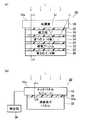
FIG. 1A is a schematic diagram illustrating a configuration of a touch panel module according to an embodiment of the present invention, and FIG. 1B is a schematic diagram illustrating an electronic apparatus according to an embodiment of the present invention. Fig.2 (a) is typical sectional drawing which shows an example of a conductive film, (b) is typical sectional drawing which shows the other example of a conductive film.
図1(a)に示すタッチパネルモジュール10は、導電フィルム12と第1のλ/4板14と偏光板16と保護層18とがこの順で、光学的透明層22を介して配置されている。さらに、導電フィルム12の保護層18側とは反対側に第2のλ/4板20が光学的透明層22を介して配置されている。導電フィルム12は、タッチセンサー部分に相当するものであり、後に詳細に説明するが、メッシュ状金属電極で構成されたメッシュ導電層が支持体に形成されたものである。
タッチパネルモジュール10では、例えば、太陽光Lが保護層18の表面18aから入射され、導電フィルム12で反射された光は保護層18の表面18a側から電子機器の使用者に観察される。なお、以下、タッチパネルモジュール10において観察される、保護層18の表面18a側のことを単に観察側ともいう。In the
In the
タッチパネルモジュール10では、上述のことから保護層18側から測定した可視光拡散反射率を0.2%以下とした。これにより、導電フィルム12のメッシュ状金属電極を視認しにくくなる。なお、可視光拡散反射率が0.2%を超える場合には、メッシュ状金属電極の視認性が上がり、メッシュ状金属電極が見えやすくなる。
なお、タッチパネルモジュール10において、導電フィルム12上に第1のλ/4板14および偏光板16を、この順で設けることで可視光拡散反射率を下げることができることを、本発明者が見出し、そのような構成にした。In the
In addition, in the
ここで、可視光拡散反射率とは、380nm〜780nmの拡散反射率を測定し、測定された拡散反射率に、JISA5759:2008の表1.1(可視光線透過率を計算するための重価係数)にある重価係数を乗じて加重平均することにより求めた値のことである。 Here, the visible light diffuse reflectance is measured by measuring the diffuse reflectance of 380 nm to 780 nm, and the measured diffuse reflectance is calculated according to Table 1.1 of JIS A5759: 2008 (the weight for calculating the visible light transmittance). It is a value obtained by multiplying the weighting coefficient in (Coefficient) by the weighted average.
可視光拡散反射率とほぼ同じ関係になる物性値としてL*があり、このL*の値も小さくすることが線見えの抑制には効果的である。本発明では、保護層18の表面18aのL*は2以下であることが好ましい。
ここで、本発明のL*とは、CIE1976L*a*b*色空間におけるL*の値のことである。
L*の値の測定方法は、上述のCIE1976L*a*b*色空間におけるL*の値を測定することができれば、特に限定されるものではなく、例えば、分光光度計で測定することができる。例えば、分光光度計スペクトロアイ(商品名 サカタインクスエンジニアリング株式会社)を用いて測定することができる。There is L* as a physical property value that has substantially the same relationship with the visible light diffuse reflectance, and it is effective to suppress the line appearance by reducing this L* value. In the present invention, L* of the
Here,L * A of the present invention, is that the value ofL * in CIE1976L* a* b* color space.
Method of measuring the L* value, if it is possible to measure the value ofL * in the above CIE1976L* a* b* color space, is not particularly limited, for example, can be measured with a spectrophotometer . For example, it can be measured using a spectrophotometer Spectroeye (trade name: Sakata Inx Engineering Co., Ltd.).
タッチパネルモジュール10を、保護層18/偏光板16/第1のλ/4板14/導電フィルム12/第2のλ/4板20の順で光学的透明層22を介して積層した構成とすることで、保護層18側から測定した可視光拡散反射率を0.2%以下にでき、保護層18の表面18aのL*を2以下にすることができる。
以下、タッチパネルモジュール10の各構成について説明する。
第1のλ/4板14と第2のλ/4板20とは同じ構成であり、いずれも位相差π/2(90°)を与えるものである。第1のλ/4板14と第2のλ/4板20により、直線偏光を楕円偏光または円偏光に変えたり、楕円偏光または円偏光を直線偏光に変えられる。第1のλ/4板14と第2のλ/4板20としては、上述の機能を発揮するものであれば、特に限定されるものではなく、公知のものを適宜用いることができる。
第1のλ/4板14と第2のλ/4板20は、例えば、ポリカーボネート(PC)基材、トリアセチルセルロース(TAC)基材、シクロオレフィンポリマー(COP)基材等で形成される。The
Hereinafter, each component of the
The first λ / 4
The first λ / 4
ここで、メッシュ導電層とλ/4板を張り合わせてタッチパネルモジュールとして使用すると、経時で絶縁抵抗が低下する場合があることがわかってきた。これはメッシュ導電層のメッシュ状金属電極がマイグレーションを起こしてしまうためである。マイグレーションはλ/4板に近い位置で顕著に発生しており、その原因はλ/4板の含水率が高く、水を吸いやすいためであることがわかった。この解決策としてλ/4板の含水率を下げることが重要である。マイグレーションを抑制するためには、第1のλ/4板14と第2のλ/4板20の平衡含水率が2%以下であることが好ましい。
第1のλ/4板14と第2のλ/4板20を、平衡含水率が小さなもので構成することで、平衡含水率を小さくすることができる。第1のλ/4板14と第2のλ/4板20に、例えば、ポリカーボネート基材またはCOP基材を用いることで平衡含水率を小さくできる。
第1のλ/4板14と第2のλ/4板20の平衡含水率の測定方法は、カールフィッシャー法を用いることができる。Here, it has been found that when a mesh conductive layer and a λ / 4 plate are bonded to each other and used as a touch panel module, the insulation resistance may decrease over time. This is because the mesh metal electrode of the mesh conductive layer causes migration. It was found that migration occurred remarkably at a position close to the λ / 4 plate because the moisture content of the λ / 4 plate was high and it was easy to absorb water. As a solution to this, it is important to reduce the water content of the λ / 4 plate. In order to suppress migration, it is preferable that the equilibrium moisture content of the first λ / 4
By configuring the first λ / 4
The Karl Fischer method can be used as a method for measuring the equilibrium water content of the first λ / 4
偏光板16は、タッチパネルモジュール10に入ってくる光に偏光を与える。導電フィルム12で反射した光は、偏光の向きが直交してしまうため偏光板16を通らない。一方、後述する液晶表示パネル32から発せられる光は偏光の向きが揃うため偏光板16を通過する。偏光板16としては、上述の機能を発揮するものであれば、特に限定されるものではなく、公知のものを適宜用いることができる。 The
保護層18は、導電フィルム12、第1のλ/4板14、および偏光板16を保護するためのものである。保護層18は、その構成は、特に限定されるものではない。例えば、ガラス、ポリカーボネート(PC)、ポリエチレンテレフタレート(PET)、アクリル樹脂(PMMA)等を用いることができる。保護層18の表面18aは、例えば、タッチ面となるが、この場合、表面18aには必要に応じてハードコート層を設けてもよい。 The
光学的透明層22は、タッチパネルモジュール10の各構成物を安定にして固定するものである。光学的透明層22は、光学的に透明で絶縁性を有するものであり、かつ安定して固定することができれば、その構成は、特に限定されるものではない。光学的透明層22としては、例えば、光学的透明な粘着剤(OCA)およびUV硬化樹脂等の光学的透明な樹脂(OCR)を用いることができる。また、光学的透明層22は部分的に中空(エアギャップ)とされていてもよい。
ここで、光学的に透明とは、光透過率が可視光波長(波長400〜800nm)において、少なくとも60%以上のことであり、好ましくは80%以上であり、より好ましくは90%以上、さらにより好ましくは95%以上のことである。The optical
Here, optically transparent means that the light transmittance is at least 60% or more, preferably 80% or more, more preferably 90% or more, in the visible light wavelength (wavelength 400 to 800 nm). More preferably, it is 95% or more.
次に、タッチパネルモジュール10の作用効果を説明する。
本実施形態のタッチパネルモジュール10では、保護層18の表面18aから入射光Liが入射された場合、入射光Liは、まず、偏光板16で特定方向に直線偏光された光のみ透過する。そして、第1のλ/4板14で円偏光に変換されて、導電フィルム12に入射し、導電フィルム12のメッシュ状金属電極等で反射する。導電フィルム12で反射した反射光Lrは、第1のλ/4板14で直線偏光に変換され、偏光板16に達する。この直線偏光された光は偏光板16の偏光の向きとはπ/2ずれているため、偏光板16を通過できない。このため、反射光Lrは外部に出射できない。このように、入射光Liが導電フィルム12で反射しても外部に出射する光量を抑制することができ、観察側から導電フィルム12のメッシュ状金属電極が視認されることが抑制される。
なお、タッチパネルモジュール10において、第1のλ/4板14と偏光板16の積層順が逆の場合には、反射光Lrが外部に出射することを抑制できず、観察側から導電フィルム12のメッシュ状金属電極の視認の抑制効果が得られない。Next, the function and effect of the
In the
In the
タッチパネルモジュール10は、電子機器に利用される。例えば、図1(b)に示すように、液晶表示パネル32(液晶表示部)と組み合わせて電子機器30とされる。この場合、タッチパネルモジュール10は、保護層18(図1(a)参照)を上にして、液晶表示パネル32の表面32a上に光学的透明層34を介して設けられる。
光学的透明層34は、タッチパネルモジュール10の光学的透明層22と同様の構成であるため、その詳細な説明は省略する。
電子機器30では、タッチパネルモジュール10に検出部36が接続される。電子機器30への接触は、指等の接触により、タッチパネルモジュール10において静電容量が変化した位置が検出部36で検出される。検出部36は静電容量式のタッチパネルの検出に利用される公知のもので構成することができる。The
Since the optical
In the
次に、電子機器30の作用効果を説明する。
電子機器30に用いられる液晶表示パネル32の表面32aから出射される光Lbは偏光していることが知られている。液晶表示パネル32からの偏光した光Lbに対して、電子機器30のタッチパネルモジュール10では、液晶表示パネル32から出射された光Lbは、第1のλ/4板20で円偏光にされ、導電フィルム12を通過し、さらに第1のλ/4板14で直線偏光にされて偏光板16に達する。この偏光板16に到達する直線偏光が偏光板16と偏光の向きが一致していれば、液晶表示パネル32からの光Lbは偏光板16で遮断されることなく通過し、タッチパネルモジュール10の表面10a(保護層18の表面18a)から外部に光Loが出射する。光Loは偏光板16で偏光されることなく出射するため、液晶表示パネル32からの光Lbの光量の減衰が抑制され、液晶表示パネル32の光量の低下を少なくして外部に液晶表示パネル32から光Lbを取り出すことができる。しかも、上述のように導電フィルム12等での反射光も抑制されており、高いコントラスト比を得ることができる。
なお、電子機器30として、タッチパネルモジュール10と液晶表示パネル32とを組み合わせたものと例にしたが、電子機器30はこれに限定されるものではない。電子機器30は、例えば、液晶表示パネル32に代えて有機EL表示パネルとした構成でもよい。電子機器30において、出射される光が偏光している表示装置を用いることが有効である。Next, functions and effects of the
It is known that the light Lb emitted from the
In addition, although the example which combined the
次に、導電フィルム12について詳細に説明する。なお、以下で説明する導電フィルム12は、本発明で利用可能なものの一例であり、これに限定されるものではない。
図2(a)は、導電フィルムの一例を示す模式的断面図であり、(b)は、導電フィルムの他の例を示す模式的断面図である。なお、図2(a)、(b)では、光学的透明層22を一部省略している。Next, the
Fig.2 (a) is typical sectional drawing which shows an example of a conductive film, (b) is typical sectional drawing which shows the other example of a conductive film. 2A and 2B, a part of the optical
例えば、導電フィルム12は、図2(a)に示すように、支持体40の表面40aに第1の検出電極42が形成され、支持体40の裏面40bに第2の検出電極44が形成されている。第1の検出電極42と第2の検出電極44は、静電容量の変化を検出するためのものである。
第1の検出電極42と第2の検出電極44は、例えば、網目状のパターンを有するメッシュ状金属電極であり、導体細線45(図3(a)、(b)参照)で構成される。
なお、第1の検出電極42と第2の検出電極44とで、それぞれ支持体40の各面にメッシュ導電層46が構成される。For example, in the
The
The
図2(a)に示すように1つの支持体40の両面に検出電極を形成することにより、支持体40が伸縮しても、第1の検出電極42と第2の検出電極44との位置関係のズレを小さくすることができる効果がある。なお、図2(a)では図示はしていないが、支持体40の各面には、第1の検出電極42および第2の検出電極44を上述の検出部36(図1(b)参照)に接続するための周辺配線が形成されている。
導電フィルム12は、図2(a)に示す構成に限定されるものではない。例えば、図2(b)に示すように表面40aに第1の検出電極42が形成された支持体40と、表面40aに第2の検出電極44が形成された支持体40とを積層した構成とすることもできる。この場合、第2の検出電極44が形成された支持体40が光学的透明層22を介して第1の検出電極42が形成された支持体40の裏面40bに積層される。
第1の検出電極42と第2の検出電極44とは、図2(a)、(b)では支持体40で分離されているが平面視直交して配置されている。As shown in FIG. 2A, by forming detection electrodes on both surfaces of one
The
The
第1の検出電極42と第2の検出電極44を構成する導体細線45(図3(a)、(b)参照)は、視認性および表示装置に配置された際に生じるモアレを低減するために、導体細線45の線幅d(図2(a)、(b)参照)はできるだけ細い方が好ましい。この点から、第1の検出電極42と第2の検出電極44の導体細線45の線幅dは10μm未満であることが好ましく、より好ましくは5μm以下である。
しかしながら、導体細線45の線幅dが細すぎると工程中に断線を生じ易くなるので、導体細線45の線幅dは、0.5μm以上が好ましく、1μm以上がより好ましい。
導体細線45の厚さは、抵抗値の観点より、0.1μm以上が好ましい。しかしながら、導体細線の厚さが厚すぎると後述する粘着層との密着が悪くなることがあるので、10μm以下が好ましい。The thin conductor wire 45 (see FIGS. 3A and 3B) that constitutes the
However, if the line width d of the conductor
The thickness of the
導体細線45は、金属で構成されるものであるが、例えば、金、銀、銅、アルミニウム等金属またはその合金で構成される。その中でも、抵抗値の観点から銀および銀合金が好ましい。また、導体細線45は、バインダを含むことにより、曲げ加工しやすくなり、かつ曲げ耐性が向上する。このため、これらにバインダを含むもので導体細線45を構成することが好ましい。バインダとしては、導電性フィルムの配線に利用されるものを適宜用いることができ、例えば、特開2013−12604号公報に記載されているゼラチン、ポリビニールアルコール(PVA)等を用いることができる。 The conductor
第1の検出電極42と第2の検出電極44を、金属または合金からなる導体細線45からなるメッシュ状金属電極とすることで、検出電極の抵抗を低くでき、タッチパネルの検出感度を良くすることができる。また、網目状のメッシュ状金属電極は、支持体40の伸縮に対して、検出電極の断線および抵抗上昇を抑制できる効果がある。
なお、タッチパネルモジュール10では金属または合金からなる導体細線45を用いているため、ITO等の透明導電材料に比して抵抗を小さくすることができる。このため、低抵抗なタッチパネルモジュール10とすることができる。By making the
Since the
メッシュ状金属電極のメッシュ形状は同じ形が規則的に配列した定型形状でも良く、ランダム形状でも良い。定型形状の場合は、正方形、菱形、正六角形が好ましく、特に菱形が好ましい。菱形の場合、その鋭角の角度は、50度〜80度であることが、表示装置とのモアレを低減する観点から好ましい。メッシュピッチは50μm〜600μmであり、メッシュの開口率は92%〜99%であることが好ましい。メッシュの開口率は、メッシュ部における導体細線の非占有面積率で定義される。
なお、メッシュ状金属電極としては、例えば、特開2011−129501号公報、および特開2013−149236号公報等に開示されている網目状のメッシュ状金属電極を用いることができる。これ以外にも、例えば、静電容量式のタッチパネルに用いられる検出電極を適宜用いることができる。The mesh shape of the mesh metal electrode may be a regular shape in which the same shape is regularly arranged, or may be a random shape. In the case of a fixed shape, a square, a rhombus, and a regular hexagon are preferable, and a rhombus is particularly preferable. In the case of a rhombus, the acute angle is preferably 50 to 80 degrees from the viewpoint of reducing moire with the display device. The mesh pitch is preferably 50 μm to 600 μm, and the mesh opening ratio is preferably 92% to 99%. The aperture ratio of the mesh is defined by the unoccupied area ratio of the conductor thin wires in the mesh portion.
In addition, as a mesh-shaped metal electrode, the mesh-shaped mesh-shaped metal electrode currently disclosed by Unexamined-Japanese-Patent No. 2011-129501, Unexamined-Japanese-Patent No. 2013-149236, etc. can be used, for example. In addition to this, for example, a detection electrode used for a capacitive touch panel can be used as appropriate.
第1の検出電極42、第2の検出電極44、周辺配線の形成方法は、特に限定されるものではない。例えば、特開2012−185813号公報の[0067]〜[0083]に記載されているように感光性ハロゲン化銀塩を含有する乳剤層を有する感光材料を露光し、現像処理を施すことによって形成することができる。また、支持体40の表面40aおよび裏面40bに、それぞれ金属箔を形成し、各金属箔上にレジストをパターン状に印刷するか、または全面塗布したレジストを露光し、現像することでパターン化して、開口部の金属をエッチングすることにより第1の検出電極42、第2の検出電極44、周辺配線を形成することができる。これ以外にも、第1の検出電極42、第2の検出電極44、周辺配線の形成方法としては、上述の導体を構成する材料の微粒子を含むペーストを印刷し、ペーストに金属めっきを施す方法、および上述の導体を構成する材料の微粒子を含むインクを用いたインクジェット法を用いる方法、上述の導体を構成する材料の微粒子を含むインクをスクリーン印刷で形成する方法、基板上に溝を有する樹脂を形成しその溝に導電インクを塗布する方法、マイクロコンタクト印刷パターニング法が挙げられる。 The method of forming the
支持体40は、第1の検出電極42および第2の検出電極44を支持するものであり、電気絶縁材料で構成される。
支持体40には、例えば、プラスチックフィルム、プラスチック板、ガラス板等を用いることができる。プラスチックフィルムおよびプラスチック板は、例えば、ポリエチレンテレフタレート(PET)、ポリエチレンナフタレート(PEN)等のポリエステル類、ポリエチレン(PE)、ポリプロピレン(PP)、ポリスチレン、エチレンビニルアセテート(EVA)、シクロオレフィンポリマー(COP)、シクロオレフィンコポリマー(COC)等のポリオレフィン類、ビニル系樹脂、その他、ポリカーボネート(PC)、ポリアミド、ポリイミド、アクリル樹脂、トリアセチルセルロース(TAC)等で構成することができる。The
As the
本実施形態では、導電フィルム12の支持体40は、波長550nmにおける面内方向のリタデーション値が40nm以下であることが好ましく、20nm以下であることがより好ましい。
例えば、支持体40をPETで構成した場合、リタデーション値は100nm以上である。リタデーション値が40nmを超えるような大きい場合、偏光の効果が薄れてしまい、可視光拡散反射率が高くなり、メッシュ状金属電極の視認性が上がり線見えが劣化する可能性がある。
支持体40には、上述のようなものが用いられる。支持体40にはシクロオレフィンポリマー(COP)として、ARTON((登録商標アートン)JSR社製)が用いられ、シクロオレフィンコポリマーとして、TOPAS((登録商標トパス)ポリプラスチック社製)が用いられる。なお、アートン、トパスのいずれも、リタデーション値が低く5〜10nm程度である。この点から、支持体40にアートンおよびトパスを用いることがより好ましい。In this embodiment, the
For example, when the
The
支持体40の波長550nmにおける面内方向リタデーション値は、支持体40の面内方向における遅相軸方向の屈折率をnxとし、支持体40の面内方向における進相軸方向の屈折率をnyとし、支持体40の厚みをtとしたとき、(nx−ny)×tで計算される値のことである。
支持体40の面内リタデーション値は、例えば、大塚電子株式会社製の低リタデーション測定装置(型式:RE−100)を用いて、測定波長550nmで測定される。
なお、支持体40が複数層の場合、リタデーション値は、各層のリタデーション値の合計が40nm以下であることが好ましく、より好ましくは20nm以下である。The in-plane retardation value of the
The in-plane retardation value of the
In addition, when the
次に、第1の検出電極42および第2の検出電極44について、図3(a)、(b)、図4を用いて具体的に説明する。なお、以下で説明する第1の検出電極42および第2の検出電極44は、本発明で利用可能なものの一例であり、これに限定されるものではない。
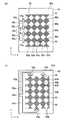
図3(a)は、第1の検出電極の電極パターンを示す模式図であり、(b)は、第2の検出電極の電極パターンを示す模式図である。図4は、本発明の実施形態の導電フィルムのメッシュ状金属電極を示す模式図である。Next, the
FIG. 3A is a schematic diagram showing an electrode pattern of the first detection electrode, and FIG. 3B is a schematic diagram showing an electrode pattern of the second detection electrode. FIG. 4 is a schematic view showing a mesh-like metal electrode of the conductive film according to the embodiment of the present invention.
図3(a)に示すように、第1の検出電極42は、例えば、表示装置の表示領域に配される第1センサ部50aに配置される。第1センサ部50aに接続された第1端子配線部52aが表示領域の外周領域、いわゆる額縁に設けられている。 As shown to Fig.3 (a), the
第1センサ部50aは、例えば、長方形状である。第1端子配線部52aのうち、第2の方向Yに平行する一辺側の周縁部には、その長さ方向中央部分に、複数の第1端子54aが第2の方向Yに配列形成されている。第1センサ部50aの一辺、第2の方向Yに平行する辺に沿って、複数の第1結線部56aが略一列に配列されている。各第1結線部56aから導出された第1端子配線パターン58aは、第1端子54aに向かって引き回されており、それぞれ対応する第1端子54aに電気的に接続されている。第1端子54aは、例えば、上述の電子機器30(図1(b)参照)の検出部36(図1(b)参照)に接続される。第1端子配線部52a、第1端子54a、第1結線部56aおよび第1端子配線パターン58aをまとめて周辺配線という。 The
第1センサ部50aには、ダイヤモンドパターン状に導体細線45が交差した第1導電パターン60a(メッシュパターン)として第1の検出電極42が配置される。第1導電パターン60aは、ダイヤモンドパターンが第1の方向Xにそれぞれ延在し、かつ第1の方向Xに直交する第2の方向Yに配列されている。また、各第1導電パターン60aは、2以上の第1大格子62aが第1の方向Xに直列に接続されている。隣接する第1大格子62a間には、これら第1大格子62aを電気的に接続する第1接続部64aが形成されている。 In the
各第1導電パターン60aの一方の端部側において、第1大格子62aの開放端には、第1結線部56aが形成されていない。各第1導電パターン60aの他方の端部側において、第1大格子62aの端部には、第1結線部56aがそれぞれ設けられている。そして、各第1導電パターン60aは、各第1結線部56aを介して、第1端子配線パターン58aに電気的に接続されている。 On one end side of each first
図3(b)に示すように、第2の検出電極44は、例えば、表示装置の表示領域に配される第2センサ部50bに配置される。第2センサ部50bに接続された第2端子配線部52bが表示領域の外周領域、いわゆる額縁に設けられている。 As shown in FIG. 3B, the
第2センサ部50bは、第1センサ部50aと重ねて配置されるものであり、長方形状である。第1センサ部50aと第2センサ部50bは平面視で交差して配置される。
第2端子配線部52bのうち、第2の方向Yに平行する一辺側の周縁部には、その長さ方向中央部分に、複数の第2端子54bが第2の方向Yに配列形成されている。第2センサ部50bの一辺、第1の方向Xに平行する辺に沿って、複数の第2結線部56b、例えば、奇数番目の第2結線部56bが略一列に配列されている。第2センサ部50bの他辺、一辺に対向する辺に沿って、複数の第2結線部56b、例えば、偶数番目の第2結線部56bが略一列に配列されている。各第2結線部56bから導出された第2端子配線パターン58bは第2端子54bに向かって引き回されており、それぞれ対応する第2端子54bに電気的に接続されている。第2端子配線部52b、第2端子54b、第2結線部56bおよび第2端子配線パターン58bをまとめて周辺配線という。The
In the second
第2センサ部50bでは、ダイヤモンドパターン状に導体細線45が交差した第2導電パターン60b(メッシュパターン)として第2の検出電極44が配置される。第2導電パターン60bは、第2の方向Yにそれぞれ延在し、かつ、第2の方向Yに直交する第1の方向Xに配列されている。各第2導電パターン60bは、2以上の第2大格子62bが第2の方向Yに直列に接続されている。隣接する第2大格子62b間には、これら第2大格子62bを電気的に接続する第2接続部64bが形成されている。 In the
各第2導電パターン60bの一方の端部側において、第2大格子62bの開放端には、第2結線部56bが形成されていない。各第2導電パターン60bの他方の端部側において、第2大格子62bの端部には、第2結線部56bがそれぞれ設けられている。そして、各第2導電パターン60bは、各第2結線部56bを介して、第2端子配線パターン58bに電気的に接続されている。 On one end side of each second
図4に示すように、第1導電パターン60aは、各第1大格子62aが、それぞれ2以上の第1小格子66aを組み合わせて構成されている。第1小格子66aの形状は、ここでは最も小さい菱形である。隣接する第1大格子62a間を接続する第1接続部64aは、第1小格子66a以上の面積であって、かつ第1大格子62aよりも小さい面積を有する第1中格子68aで構成される。
なお、第2導電パターン60bは、第1導電パターン60aと同じ構成であるため、同じく図4を用いて説明する。
第2導電パターン60bは、各第2大格子62bが、それぞれ2以上の第2小格子66bを組み合わせて構成されている。第2小格子66bの形状は、ここでは最も小さい菱形であり、上述した1つのメッシュ形状と同一のまたは相似する形状である。隣接する第2大格子62b間を接続する第2接続部64bは、第2小格子66b以上の面積であって、かつ第2大格子62bよりも小さい面積を有する第2中格子68bで構成される。As shown in FIG. 4, in the first
The second
In the second
以上のように、導電フィルム12について、検出電極が支持体40等の電気絶縁性材料を介して配置される構成の静電容量式のものを例にして説明したが、本発明は静電容量式に限定されるものではない。導電フィルム12としては、例えば、特開2010−16067号公報等に開示されているように電極の交差部のみに絶縁膜を設け、絶縁膜上に形成したブリッジ配線で接続する構成の導電性フィルム、およびUS2012/0262414等に開示されている交差部がない電極構成のように検出電極が基板の片側にしかない構成の導電性フィルムであってもよい。 As described above, the
本発明は、基本的に以上のように構成されるものである。以上、本発明のタッチパネルモジュールおよび電子機器について詳細に説明したが、本発明は上記実施形態に限定されず、本発明の主旨を逸脱しない範囲において、種々の改良または変更をしてもよいのはもちろんである。 The present invention is basically configured as described above. The touch panel module and the electronic device of the present invention have been described in detail above, but the present invention is not limited to the above-described embodiment, and various improvements or modifications may be made without departing from the spirit of the present invention. Of course.
以下、本発明のタッチパネルモジュールの効果について具体的に説明する。
本実施例では、実施例1〜6および比較例1〜5のタッチパネルモジュールを作製し、可視光拡散反射率、L*を測定した。さらに、線見えを評価した。なお、マイグレーションについては、露光パターンを後縦するマイグレーション試験パターンに変えて作製したサンプルを評価した。Hereinafter, the effect of the touch panel module of the present invention will be specifically described.
In this example, the touch panel modules of Examples 1 to 6 and Comparative Examples 1 to 5 were produced, and the visible light diffuse reflectance and L * were measured. Furthermore, the line appearance was evaluated. As for migration, samples prepared by changing the exposure pattern to a migration test pattern that is vertically longitudinal were evaluated.
実施例1〜6のタッチパネルモジュールは、図1(a)に示すタッチパネルモジュールと同じ構成であるため、その詳細な説明は省略する。比較例1〜5のタッチパネルモジュールは、図5に示すタッチパネルモジュール70と同じ構成である。図5に示すタッチパネルモジュール70は、図1(a)に示すタッチパネルモジュール10に比して第1のλ/4板14、偏光板16および第2のλ/4板20が設けられておらず、導電フィルム12上に保護層18が光学的透明層22を介して設けられ、導電フィルム12の下に保護フィルム72が光学的透明層22を介して設けられたものである。
なお、下記表1では、層構成の欄に、図1(a)に示す構成を「偏光板+λ/4板」と表し、図5に示す構成を「通常構成」と表す。また、下記表1では「−」はないことを表す。The touch panel modules of Examples 1 to 6 have the same configuration as the touch panel module shown in FIG. The touch panel modules of Comparative Examples 1 to 5 have the same configuration as the
In the following Table 1, in the column of the layer configuration, the configuration shown in FIG. 1A is expressed as “polarizing plate + λ / 4 plate”, and the configuration shown in FIG. 5 is expressed as “normal configuration”. In Table 1 below, “-” is not present.
また、実施例1〜6および比較例1〜5のタッチパネルモジュールでは、メッシュ状金属電極のパターンには、図6(a)に示す露光パターン80を用いた。なお、図6(a)では露光パターン80は一部しか表示していない。
露光パターン80は、ダイヤモンドパターンが一方向につながっており、さらに図示はしないが、一方向と直交する方向にも配置されている。露光パターン80では、細線パターン82で菱形状のメッシュ84(鋭角90度)が構成されている。メッシュピッチPwは、菱形状のメッシュ84の対向する辺の間の距離のことである。下記表1に示すメッシュピッチとは、図6(a)に示すメッシュピッチPwのことである。下記表1に示す線幅は、導体細線45の幅dのことであり、露光パターン80では細線パターン82の幅wである。露光の際に露光パターン80のメッシュピッチPwと幅wを、下記表1に示すメッシュピッチと線幅の値となるように調整した。In the touch panel modules of Examples 1 to 6 and Comparative Examples 1 to 5, the
The
マイグレーションの評価には、図6(b)に示すマイグレーション試験パターン90を用いた。マイグレーション試験パターン90は、IPC−TM650orSM840に準拠したパターンであり、ライン幅が50μm、スペース幅が50μmで、ライン数は17本/18本である。マイグレーション試験パターン90のことを、くし型パターン電極ともいう。マイグレーションの評価には、くし型パターン電極とした以外は、実施例1〜6および比較例1〜5のタッチパネルモジュールと同様の構成のサンプルを用いた。 For the migration evaluation, a
実施例1〜6では導電フィルムの支持体にシクロオレフィンポリマー(アートン(登録商標))を用いた。支持体はいずれも厚みが40μmである。
実施例1〜6、比較例1〜5のタッチパネルモジュールでは、保護層に厚みが700μmのガラスを用いた。偏光板に厚みが100μmの偏光層入りTACフィルムを用いた。
比較例1〜4のタッチパネルモジュールには、保護フィルム72として厚みが50μmのTACを用いた。比較例5のタッチパネルモジュールには、保護フィルム72として厚みが40μmのシクロオレフィンポリマー(アートン(登録商標))を用いた。In Examples 1 to 6, a cycloolefin polymer (Arton (registered trademark)) was used as the support of the conductive film. All the supports have a thickness of 40 μm.
In the touch panel modules of Examples 1 to 6 and Comparative Examples 1 to 5, glass having a thickness of 700 μm was used for the protective layer. A polarizing layer-containing TAC film having a thickness of 100 μm was used for the polarizing plate.
In the touch panel modules of Comparative Examples 1 to 4, TAC having a thickness of 50 μm was used as the
実施例1〜6のタッチパネルモジュールでは、第1のλ/4板および第2のλ/4板には、同じ材質のものを用いた。第1のλ/4板および第2のλ/4板については材質を下記表1に示す。表1中、TACとは、富士フイルム社製のTAC(トリアセチルセルロース)のλ/4板を示す。PC(ポリカーボネート)とは、帝人社製ピュアエース(登録商標) TT−138のλ/4板を示す。COP(シクロオレフィンポリマー)とは、JSR社製のアートン(登録商標)のλ/4板を示す。
なお、第1のλ/4板および第2のλ/4板は、いずれも厚みが50μmである。
光学的透明層22には厚みが50μmの共同技研化学社製のMGSFシリーズのものを用いた。In the touch panel modules of Examples 1 to 6, the same material was used for the first λ / 4 plate and the second λ / 4 plate. The materials of the first λ / 4 plate and the second λ / 4 plate are shown in Table 1 below. In Table 1, TAC refers to a TAC (triacetyl cellulose) λ / 4 plate manufactured by Fuji Film. PC (polycarbonate) indicates a λ / 4 plate of Teijin's Pure Ace (registered trademark) TT-138. COP (cycloolefin polymer) refers to an Arton (registered trademark) λ / 4 plate manufactured by JSR.
The first λ / 4 plate and the second λ / 4 plate both have a thickness of 50 μm.
As the optical
以下、導電フィルムの作製方法について説明する。 Hereinafter, a method for producing a conductive film will be described.
(ハロゲン化銀乳剤の調製)
38℃、pH4.5に保たれた下記1液に、下記の2液および3液の各々90%に相当する量を攪拌しながら同時に20分間にわたって加え、0.16μmの核粒子を形成した。続いて下記4液および5液を8分間にわたって加え、さらに、下記の2液および3液の残りの10%の量を2分間にわたって加え、0.21μmまで成長させた。さらに、ヨウ化カリウム0.15gを加え、5分間熟成し粒子形成を終了した。(Preparation of silver halide emulsion)
To the following 1 liquid maintained at 38 ° C. and pH 4.5, an amount corresponding to 90% of each of the following 2 and 3 liquids was simultaneously added over 20 minutes while stirring to form 0.16 μm core particles. Subsequently, the following 4 and 5 solutions were added over 8 minutes, and the remaining 10% of the following 2 and 3 solutions were added over 2 minutes to grow to 0.21 μm. Further, 0.15 g of potassium iodide was added and ripened for 5 minutes to complete the grain formation.
1液:
水 750ml
ゼラチン 9g
塩化ナトリウム 3g
1,3−ジメチルイミダゾリジン−2−チオン 20mg
ベンゼンチオスルホン酸ナトリウム 10mg
クエン酸 0.7g
2液:
水 300ml
硝酸銀 150g
3液:
水 300ml
塩化ナトリウム 38g
臭化カリウム 32g
ヘキサクロロイリジウム(III)酸カリウム
(0.005%KCl 20%水溶液) 8ml
ヘキサクロロロジウム酸アンモニウム
(0.001%NaCl 20%水溶液) 10ml
4液:
水 100ml
硝酸銀 50g
5液:
水 100ml
塩化ナトリウム 13g
臭化カリウム 11g
黄血塩 5mg1 liquid:
750 ml of water
9g gelatin
Sodium chloride 3g
1,3-Dimethylimidazolidine-2-thione 20mg
Sodium benzenethiosulfonate 10mg
Citric acid 0.7g
Two liquids:
300 ml of water
150 g silver nitrate
3 liquids:
300 ml of water
Sodium chloride 38g
Potassium bromide 32g
Potassium hexachloroiridium (III) (0.005
Ammonium hexachlororhodate
(0.001
4 liquids:
100ml water
Silver nitrate 50g
5 liquids:
100ml water
Sodium chloride 13g
Potassium bromide 11g
Yellow blood salt 5mg
その後、常法に従い、フロキュレーション法によって水洗した。具体的には、温度を35℃に下げ、硫酸を用いてハロゲン化銀が沈降するまでpHを下げた(pH3.6±0.2の範囲であった)。次に、上澄み液を約3リットル除去した(第一水洗)。さらに3リットルの蒸留水を加えてから、ハロゲン化銀が沈降するまで硫酸を加えた。再度、上澄み液を3リットル除去した(第二水洗)。第二水洗と同じ操作をさらに1回繰り返して(第三水洗)、水洗・脱塩工程を終了した。水洗・脱塩後の乳剤をpH6.4、pAg7.5に調整し、ゼラチン3.9g、ベンゼンチオスルホン酸ナトリウム10mg、ベンゼンチオスルフィン酸ナトリウム3mg、チオ硫酸ナトリウム15mgと塩化金酸10mgを加え55℃にて最適感度を得るように化学増感を施し、安定剤として1,3,3a,7−テトラアザインデン100mg、防腐剤としてプロキセル(商品名、ICI Co.,Ltd.製)100mgを加えた。最終的に得られた乳剤は、沃化銀を0.08モル%含み、塩臭化銀の比率を塩化銀70モル%、臭化銀30モル%とする、平均粒子径0.22μm、変動係数9%のヨウ塩臭化銀立方体粒子乳剤であった。 Then, it washed with water by the flocculation method according to a conventional method. Specifically, the temperature was lowered to 35 ° C., and the pH was lowered using sulfuric acid until the silver halide precipitated (the pH was in the range of 3.6 ± 0.2). Next, about 3 liters of the supernatant was removed (first water washing). Further, 3 liters of distilled water was added, and sulfuric acid was added until the silver halide settled. Again, 3 liters of the supernatant was removed (second water wash). The same operation as the second water washing was further repeated once (third water washing) to complete the water washing / desalting step. The emulsion after washing with water and desalting was adjusted to pH 6.4 and pAg 7.5, and gelatin 3.9 g, sodium benzenethiosulfonate 10 mg, sodium benzenethiosulfinate 3 mg, sodium thiosulfate 15 mg and
(感光性層形成用組成物の調製)
上記乳剤に1,3,3a,7−テトラアザインデン1.2×10⁻⁴モル/モルAg、ハイドロキノン1.2×10−2モル/モルAg、クエン酸3.0×10−4モル/モルAg、2,4−ジクロロ−6−ヒドロキシ−1,3,5−トリアジンナトリウム塩0.90g/モルAgを添加し、クエン酸を用いて塗布液pHを5.6に調整して、感光性層形成用組成物を得た。(Preparation of photosensitive layer forming composition)
1,3,3a, 7-tetraazaindene 1.2 × 10⁻⁴ mol / mol Ag, hydroquinone 1.2 × 10⁻² mol / mol Ag, citric acid 3.0 × 10⁻⁴ mol / Mole Ag, 2,4-dichloro-6-hydroxy-1,3,5-triazine sodium salt 0.90 g / mole Ag was added, and the coating solution pH was adjusted to 5.6 using citric acid, and the photosensitivity was obtained. A composition for forming a conductive layer was obtained.
(感光性層形成工程)
支持体にコロナ放電処理を施した後、支持体の両面に、下塗層として厚み0.1μmのゼラチン層、さらに下塗層上に光学濃度が約1.0で現像液のアルカリにより脱色する染料を含むアンチハレーション層を設けた。上記アンチハレーション層の上に、上記感光性層形成用組成物を塗布し、さらに厚み0.15μmのゼラチン層を設け、両面に感光性層が形成された支持体を得た。両面に感光性層が形成された支持体をフィルムAとする。形成された感光性層は、銀量6.0g/m2、ゼラチン量1.0g/m2であった。(Photosensitive layer forming step)
After the corona discharge treatment is applied to the support, a gelatin layer having a thickness of 0.1 μm is formed on both sides of the support as a subbing layer, and the optical density is about 1.0 on the subbing layer and decolorized by alkali of the developer. An antihalation layer containing a dye was provided. On the antihalation layer, the photosensitive layer forming composition was applied, a gelatin layer having a thickness of 0.15 μm was further provided, and a support having a photosensitive layer formed on both sides was obtained. Let the support body in which the photosensitive layer was formed in both surfaces be the film A. FIG. The formed photosensitive layer had a silver amount of 6.0 g / m2 and a gelatin amount of 1.0 g / m2 .
(露光現像工程)
上記フィルムAの両面に、上述の図6(a)の電極パターンが直交するようにフォトマスクを介し、高圧水銀ランプを光源とした平行光を用いて露光を行った。露光後、下記の現像液で現像し、さらに定着液(商品名:CN16X用N3X−R、富士フィルム社製)を用いて現像処理を行った。さらに、純水でリンスし、乾燥することで、両面にAg細線からなる電極パターンとゼラチン層とが形成された支持体を得た。ゼラチン層はAg細線間に形成されていた。得られたフィルムをフィルムBとする。(Exposure development process)
Both surfaces of the film A were exposed using parallel light using a high-pressure mercury lamp as a light source through a photomask so that the electrode patterns shown in FIG. After the exposure, development was performed with the following developer, and further development was performed using a fixing solution (trade name: N3X-R for CN16X, manufactured by Fuji Film Co., Ltd.). Furthermore, by rinsing with pure water and drying, a support having an electrode pattern made of Ag fine wires and a gelatin layer formed on both sides was obtained. The gelatin layer was formed between the Ag fine wires. The resulting film is referred to as film B.
(現像液の組成)
現像液1リットル(L)中に、以下の化合物が含まれる。
ハイドロキノン 0.037mol/L
N−メチルアミノフェノール 0.016mol/L
メタホウ酸ナトリウム 0.140mol/L
水酸化ナトリウム 0.360mol/L
臭化ナトリウム 0.031mol/L
メタ重亜硫酸カリウム 0.187mol/L(Developer composition)
The following compounds are contained in 1 liter (L) of the developer.
Hydroquinone 0.037mol / L
N-methylaminophenol 0.016 mol / L
Sodium metaborate 0.140 mol / L
Sodium hydroxide 0.360 mol / L
Sodium bromide 0.031 mol / L
Potassium metabisulfite 0.187 mol / L
(加熱工程)
上記フィルムBに対して、120℃の過熱蒸気槽に130秒間静置して、加熱処理を行った。加熱処理後のフィルムをフィルムCとする。(Heating process)
The film B was left to stand in a superheated steam bath at 120 ° C. for 130 seconds and subjected to heat treatment. The film after the heat treatment is referred to as film C.
(ゼラチン分解処理)
フィルムCに対して、タンパク質分解酵素(ナガセケムテックス社製ビオプラーゼAL−15FG)の水溶液(タンパク質分解酵素の濃度:0.5質量%、液温:40℃)に120秒浸漬した。フィルムCを水溶液から取り出し、温水(液温:50℃)に120秒間浸漬し、洗浄した。ゼラチン分解処理後のフィルムをフィルムDとする。このフィルムDが導電フィルムである。(Gelatin decomposition treatment)
The film C was immersed in an aqueous solution (proteolytic enzyme concentration: 0.5% by mass, liquid temperature: 40 ° C.) of a proteolytic enzyme (Biosease AL-15FG manufactured by Nagase ChemteX Corporation) for 120 seconds. The film C was taken out from the aqueous solution, immersed in warm water (liquid temperature: 50 ° C.) for 120 seconds and washed. The film after gelatin degradation is designated as film D. This film D is a conductive film.
(タッチパネルモジュール形成工程)
さらに、導電フィルムに、厚みが50μmの光学的透明層(共同技研化学社製のMGSFシリーズ)を用いて、第1のλ/4板、偏光板、保護層および第2のλ/4板を、実施例1〜6および比較例1〜5の各構成に応じて貼合してタッチパネルモジュールを得た。(Touch panel module formation process)
Furthermore, the first λ / 4 plate, the polarizing plate, the protective layer, and the second λ / 4 plate are formed on the conductive film using an optical transparent layer (MGSF series manufactured by Kyodo Giken Chemical Co., Ltd.) having a thickness of 50 μm. And it bonded according to each structure of Examples 1-6 and Comparative Examples 1-5, and obtained the touch panel module.
マイグレーション評価用の実施例1〜6および比較例1〜5のサンプルは、支持体の片面に、図6(b)に示すマイグレーション試験パターン90で露光する点以外は、上述のタッチパネルモジュールの作製方法と同様にして作製した。このため、作製方法の詳細な説明については省略する。 The samples of Examples 1 to 6 and Comparative Examples 1 to 5 for migration evaluation are the above-described touch panel module manufacturing methods except that one side of the support is exposed with the
(可視光拡散反射率)
実施例1〜6、比較例1〜5のタッチパネルモジュールについて、保護層の表面を、V−670 紫外可視近赤外分光光度計(日本分光社製)を使用して、380nm〜780nmの拡散反射率を測定した。そして、測定して得られた拡散反射率に、JISA5759:2008の表1.1(可視光線透過率を計算するための重価係数)にある重価係数を乗じて加重平均して可視光拡散反射率を求めた。
(L*の測定)
実施例1〜6、比較例1〜5のタッチパネルモジュールについて、保護層の表面をスペクトロアイ分光光度計(サカタインクスエンジニアリング社製)を用いて、L*を測定した。(Visible light diffuse reflectance)
For the touch panel modules of Examples 1 to 6 and Comparative Examples 1 to 5, the surface of the protective layer was diffusely reflected at 380 nm to 780 nm using a V-670 ultraviolet-visible near-infrared spectrophotometer (manufactured by JASCO Corporation). The rate was measured. Then, the diffuse reflectance obtained by the measurement is multiplied by the weight coefficient in Table 1.1 (the weight coefficient for calculating the visible light transmittance) of JISA5759: 2008, and the weighted average is used to diffuse the visible light. The reflectance was determined.
(Measurement of L* )
For the touch panel modules of Examples 1 to 6 and Comparative Examples 1 to 5, L* was measured on the surface of the protective layer using a spectroeye spectrophotometer (manufactured by Sakata Inx Engineering).
(λ/4板の平衡含水率)
第1のλ/4板と第2のλ/4板の平衡含水率の測定は、いずれもカールフィッシャー法を用いて測定した。温度25℃相対湿度80%の環境で24h調湿し、ベースを含水させる。その後、カールフィッシャー法で絶対乾燥重量を測定し、平衡含水率を求めた。
(保護フィルムの平衡含水率)
保護フィルムの平衡含水率の測定は、第1のλ/4板と第2のλ/4板の平衡含水率の測定と同じく、上述のカールフィッシャー法を用いて測定した。このため、保護フィルムの平衡含水率の測定方法についての詳細な説明は省略する。(Equilibrium moisture content of λ / 4 plate)
The equilibrium water content of the first λ / 4 plate and the second λ / 4 plate was measured using the Karl Fischer method. The humidity is adjusted for 24 hours in an environment of a temperature of 25 ° C. and a relative humidity of 80%, and the base is hydrated. Thereafter, the absolute dry weight was measured by the Karl Fischer method, and the equilibrium water content was determined.
(Equilibrium moisture content of protective film)
The equilibrium moisture content of the protective film was measured using the above-mentioned Karl Fischer method in the same manner as the equilibrium moisture content of the first λ / 4 plate and the second λ / 4 plate. For this reason, detailed description about the measuring method of the equilibrium moisture content of a protective film is abbreviate | omitted.
(線見え評価)
実施例1〜6、比較例1〜5のタッチパネルモジュールについて、太陽光光源下で線見えを観察し、以下の評価基準の評価点にて評価した。評価A、B、Cが実用可能な範囲である。
評価点
「A」:線(メッシュ状金属電極)が全く見えない
「B」:線(メッシュ状金属電極)がほとんど見えない
「C」:線(メッシュ状金属電極)が若干見える
「D」:線(メッシュ状金属電極)がよく見える(Evaluation of line appearance)
About the touch panel modules of Examples 1 to 6 and Comparative Examples 1 to 5, line appearance was observed under a sunlight light source, and evaluation was performed using the following evaluation criteria. Evaluations A, B, and C are in a practical range.
Evaluation point “A”: Line (mesh-like metal electrode) is completely invisible “B”: Line (mesh-like metal electrode) is hardly seen “C”: Line (mesh-like metal electrode) is slightly visible “D”: Lines (mesh-like metal electrodes) are clearly visible
(マイグレーション評価)
マイグレーション評価用の実施例1〜6および比較例1〜5のサンプルを温度85℃相対湿度85%の湿熱雰囲気下に静置した。そして、マイグレーション評価用の実施例1〜6および比較例1〜5のサンプルの両方の端部92(図6(b)参照)に配線を接続し、片側から直流5Vの電流を連続的に印加した。一定時間後、温度85℃相対湿度85%の湿熱雰囲気下から取り出し、アドバンテスト社製のR8340Aを用い、直流5Vの印加電圧をかけ、絶縁性抵抗を測定した。その後、マイグレーションを、以下の評価基準に従って評価した。評価A、B、Cが実用可能な範囲である。
「A」:500時間以上、絶縁抵抗値が1010Ω以上であった場合
「B」:200時間以上500時間未満で絶縁抵抗値が1010Ω未満まで低下した場合
「C」:50時間以上200時間未満で絶縁抵抗値が1010Ω未満まで低下した場合
「D」:50時間未満で絶縁抵抗値が1010Ω未満まで低下した場合(Migration evaluation)
The samples of Examples 1 to 6 and Comparative Examples 1 to 5 for migration evaluation were allowed to stand in a humid heat atmosphere at a temperature of 85 ° C. and a relative humidity of 85%. And wiring is connected to both ends 92 (refer to Drawing 6 (b)) of the samples of Examples 1-6 for comparative evaluation and comparative examples 1-5, and direct-current 5V current is applied continuously from one side. did. After a certain period of time, the sample was taken out from a moist and heat atmosphere at a temperature of 85 ° C. and a relative humidity of 85%, and an R8340A manufactured by Advantest Corporation was applied to apply an applied voltage of DC 5V to measure the insulation resistance. Thereafter, migration was evaluated according to the following evaluation criteria. Evaluations A, B, and C are in a practical range.
“A”: When 500 hours or more and the insulation resistance value is 1010 Ω or more “B”: When the insulation resistance value drops to less than 1010 Ω after 200 hours or more and less than 500 hours “C”: 50 hours or more When the insulation resistance value decreases to less than 1010 Ω in less than 200 hours “D”: When the insulation resistance value decreases to less than 1010 Ω in less than 50 hours

上記表1に示すように、実施例1〜6は、いずれも線見えについて高い評価を得ることができ、メッシュ状金属電極の視認性が低い。実施例1〜6では、λ/4板の平衡含水率が2%以下であると、λ/4板があってもマイグレーションの評価が高い。
一方、比較例1〜5は、線見えについて高い評価を得ることができず、メッシュ状金属電極の視認性が高い。
なお、比較例5のタッチパネルモジュール70は保護フィルムの平衡含水率が2%以下の構成であるため、マイグレーションは良い結果となるが、上述のように線見えについて高い評価は得られていない。As shown in Table 1 above, all of Examples 1 to 6 can obtain high evaluation for line appearance, and the visibility of the mesh-like metal electrode is low. In Examples 1 to 6, when the equilibrium moisture content of the λ / 4 plate is 2% or less, the evaluation of migration is high even with the λ / 4 plate.
On the other hand, Comparative Examples 1-5 cannot obtain high evaluation about line appearance, and the visibility of a mesh-shaped metal electrode is high.
In addition, since the
10、70 タッチパネルモジュール
12 導電フィルム
14 第1のλ/4板
16 偏光板
18 保護層
20 第2のλ/4板
22、34 光学的透明層
30 電子機器
32 液晶表示パネル
36 検出部
40 支持体
42 第1の検出電極
44 第2の検出電極
45 導体細線
46 メッシュ導電層
80 露光パターン
90 マイグレーション試験パターンDESCRIPTION OF
Claims (6)
Translated fromJapaneseさらに、前記導電フィルムの前記保護層側とは反対側にλ/4板が配置されており、
前記保護層側から測定した可視光拡散反射率が0.12%以下であることを特徴とするタッチパネルモジュール。A conductive film, a λ / 4 plate, a polarizing plate and a protective layer in which a mesh conductive layer composed of a mesh-like metal electrode is formed on a support are arranged in this order,
Furthermore, a λ / 4 plate is arranged on the side opposite to the protective layer side of the conductive film,
The touch panel module, wherein the visible light diffuse reflectance measured from the protective layer side is0.12 % or less.
Priority Applications (4)
| Application Number | Priority Date | Filing Date | Title |
|---|---|---|---|
| JP2014061317AJP6204858B2 (en) | 2014-03-25 | 2014-03-25 | Touch panel module and electronic device |
| PCT/JP2015/052951WO2015146289A1 (en) | 2014-03-25 | 2015-02-03 | Touch panel module and electronic apparatus |
| TW104105203ATWI634466B (en) | 2014-03-25 | 2015-02-16 | Touch panel module and electronic device |
| US15/234,205US10101861B2 (en) | 2014-03-25 | 2016-08-11 | Touch panel module and electronic apparatus |
Applications Claiming Priority (1)
| Application Number | Priority Date | Filing Date | Title |
|---|---|---|---|
| JP2014061317AJP6204858B2 (en) | 2014-03-25 | 2014-03-25 | Touch panel module and electronic device |
Publications (2)
| Publication Number | Publication Date |
|---|---|
| JP2015184958A JP2015184958A (en) | 2015-10-22 |
| JP6204858B2true JP6204858B2 (en) | 2017-09-27 |
Family
ID=54194829
Family Applications (1)
| Application Number | Title | Priority Date | Filing Date |
|---|---|---|---|
| JP2014061317AActiveJP6204858B2 (en) | 2014-03-25 | 2014-03-25 | Touch panel module and electronic device |
Country Status (4)
| Country | Link |
|---|---|
| US (1) | US10101861B2 (en) |
| JP (1) | JP6204858B2 (en) |
| TW (1) | TWI634466B (en) |
| WO (1) | WO2015146289A1 (en) |
Families Citing this family (398)
| Publication number | Priority date | Publication date | Assignee | Title |
|---|---|---|---|---|
| US20070084897A1 (en) | 2003-05-20 | 2007-04-19 | Shelton Frederick E Iv | Articulating surgical stapling instrument incorporating a two-piece e-beam firing mechanism |
| US9060770B2 (en) | 2003-05-20 | 2015-06-23 | Ethicon Endo-Surgery, Inc. | Robotically-driven surgical instrument with E-beam driver |
| US11998198B2 (en) | 2004-07-28 | 2024-06-04 | Cilag Gmbh International | Surgical stapling instrument incorporating a two-piece E-beam firing mechanism |
| US11890012B2 (en) | 2004-07-28 | 2024-02-06 | Cilag Gmbh International | Staple cartridge comprising cartridge body and attached support |
| US8215531B2 (en) | 2004-07-28 | 2012-07-10 | Ethicon Endo-Surgery, Inc. | Surgical stapling instrument having a medical substance dispenser |
| US9072535B2 (en) | 2011-05-27 | 2015-07-07 | Ethicon Endo-Surgery, Inc. | Surgical stapling instruments with rotatable staple deployment arrangements |
| US11484312B2 (en) | 2005-08-31 | 2022-11-01 | Cilag Gmbh International | Staple cartridge comprising a staple driver arrangement |
| US10159482B2 (en) | 2005-08-31 | 2018-12-25 | Ethicon Llc | Fastener cartridge assembly comprising a fixed anvil and different staple heights |
| US7669746B2 (en) | 2005-08-31 | 2010-03-02 | Ethicon Endo-Surgery, Inc. | Staple cartridges for forming staples having differing formed staple heights |
| US11246590B2 (en) | 2005-08-31 | 2022-02-15 | Cilag Gmbh International | Staple cartridge including staple drivers having different unfired heights |
| US9237891B2 (en) | 2005-08-31 | 2016-01-19 | Ethicon Endo-Surgery, Inc. | Robotically-controlled surgical stapling devices that produce formed staples having different lengths |
| US7934630B2 (en) | 2005-08-31 | 2011-05-03 | Ethicon Endo-Surgery, Inc. | Staple cartridges for forming staples having differing formed staple heights |
| US20070106317A1 (en) | 2005-11-09 | 2007-05-10 | Shelton Frederick E Iv | Hydraulically and electrically actuated articulation joints for surgical instruments |
| US7845537B2 (en) | 2006-01-31 | 2010-12-07 | Ethicon Endo-Surgery, Inc. | Surgical instrument having recording capabilities |
| US20110295295A1 (en) | 2006-01-31 | 2011-12-01 | Ethicon Endo-Surgery, Inc. | Robotically-controlled surgical instrument having recording capabilities |
| US8186555B2 (en) | 2006-01-31 | 2012-05-29 | Ethicon Endo-Surgery, Inc. | Motor-driven surgical cutting and fastening instrument with mechanical closure system |
| US8708213B2 (en) | 2006-01-31 | 2014-04-29 | Ethicon Endo-Surgery, Inc. | Surgical instrument having a feedback system |
| US11224427B2 (en) | 2006-01-31 | 2022-01-18 | Cilag Gmbh International | Surgical stapling system including a console and retraction assembly |
| US20120292367A1 (en) | 2006-01-31 | 2012-11-22 | Ethicon Endo-Surgery, Inc. | Robotically-controlled end effector |
| US8820603B2 (en) | 2006-01-31 | 2014-09-02 | Ethicon Endo-Surgery, Inc. | Accessing data stored in a memory of a surgical instrument |
| US11793518B2 (en) | 2006-01-31 | 2023-10-24 | Cilag Gmbh International | Powered surgical instruments with firing system lockout arrangements |
| US20110024477A1 (en) | 2009-02-06 | 2011-02-03 | Hall Steven G | Driven Surgical Stapler Improvements |
| US11278279B2 (en) | 2006-01-31 | 2022-03-22 | Cilag Gmbh International | Surgical instrument assembly |
| US7753904B2 (en) | 2006-01-31 | 2010-07-13 | Ethicon Endo-Surgery, Inc. | Endoscopic surgical instrument with a handle that can articulate with respect to the shaft |
| US8992422B2 (en) | 2006-03-23 | 2015-03-31 | Ethicon Endo-Surgery, Inc. | Robotically-controlled endoscopic accessory channel |
| US8322455B2 (en) | 2006-06-27 | 2012-12-04 | Ethicon Endo-Surgery, Inc. | Manually driven surgical cutting and fastening instrument |
| US10568652B2 (en) | 2006-09-29 | 2020-02-25 | Ethicon Llc | Surgical staples having attached drivers of different heights and stapling instruments for deploying the same |
| US11980366B2 (en) | 2006-10-03 | 2024-05-14 | Cilag Gmbh International | Surgical instrument |
| US8684253B2 (en) | 2007-01-10 | 2014-04-01 | Ethicon Endo-Surgery, Inc. | Surgical instrument with wireless communication between a control unit of a robotic system and remote sensor |
| US11291441B2 (en) | 2007-01-10 | 2022-04-05 | Cilag Gmbh International | Surgical instrument with wireless communication between control unit and remote sensor |
| US8632535B2 (en) | 2007-01-10 | 2014-01-21 | Ethicon Endo-Surgery, Inc. | Interlock and surgical instrument including same |
| US20080169333A1 (en) | 2007-01-11 | 2008-07-17 | Shelton Frederick E | Surgical stapler end effector with tapered distal end |
| US11039836B2 (en) | 2007-01-11 | 2021-06-22 | Cilag Gmbh International | Staple cartridge for use with a surgical stapling instrument |
| US7673782B2 (en) | 2007-03-15 | 2010-03-09 | Ethicon Endo-Surgery, Inc. | Surgical stapling instrument having a releasable buttress material |
| US8931682B2 (en) | 2007-06-04 | 2015-01-13 | Ethicon Endo-Surgery, Inc. | Robotically-controlled shaft based rotary drive systems for surgical instruments |
| US11564682B2 (en) | 2007-06-04 | 2023-01-31 | Cilag Gmbh International | Surgical stapler device |
| US7753245B2 (en) | 2007-06-22 | 2010-07-13 | Ethicon Endo-Surgery, Inc. | Surgical stapling instruments |
| US11849941B2 (en) | 2007-06-29 | 2023-12-26 | Cilag Gmbh International | Staple cartridge having staple cavities extending at a transverse angle relative to a longitudinal cartridge axis |
| US8636736B2 (en) | 2008-02-14 | 2014-01-28 | Ethicon Endo-Surgery, Inc. | Motorized surgical cutting and fastening instrument |
| US11986183B2 (en) | 2008-02-14 | 2024-05-21 | Cilag Gmbh International | Surgical cutting and fastening instrument comprising a plurality of sensors to measure an electrical parameter |
| JP5410110B2 (en) | 2008-02-14 | 2014-02-05 | エシコン・エンド−サージェリィ・インコーポレイテッド | Surgical cutting / fixing instrument with RF electrode |
| US9179912B2 (en) | 2008-02-14 | 2015-11-10 | Ethicon Endo-Surgery, Inc. | Robotically-controlled motorized surgical cutting and fastening instrument |
| US8758391B2 (en) | 2008-02-14 | 2014-06-24 | Ethicon Endo-Surgery, Inc. | Interchangeable tools for surgical instruments |
| US7866527B2 (en) | 2008-02-14 | 2011-01-11 | Ethicon Endo-Surgery, Inc. | Surgical stapling apparatus with interlockable firing system |
| US7819298B2 (en) | 2008-02-14 | 2010-10-26 | Ethicon Endo-Surgery, Inc. | Surgical stapling apparatus with control features operable with one hand |
| US8573465B2 (en) | 2008-02-14 | 2013-11-05 | Ethicon Endo-Surgery, Inc. | Robotically-controlled surgical end effector system with rotary actuated closure systems |
| US9585657B2 (en) | 2008-02-15 | 2017-03-07 | Ethicon Endo-Surgery, Llc | Actuator for releasing a layer of material from a surgical end effector |
| US11648005B2 (en) | 2008-09-23 | 2023-05-16 | Cilag Gmbh International | Robotically-controlled motorized surgical instrument with an end effector |
| US9386983B2 (en) | 2008-09-23 | 2016-07-12 | Ethicon Endo-Surgery, Llc | Robotically-controlled motorized surgical instrument |
| US8210411B2 (en) | 2008-09-23 | 2012-07-03 | Ethicon Endo-Surgery, Inc. | Motor-driven surgical cutting instrument |
| US9005230B2 (en) | 2008-09-23 | 2015-04-14 | Ethicon Endo-Surgery, Inc. | Motorized surgical instrument |
| US8608045B2 (en) | 2008-10-10 | 2013-12-17 | Ethicon Endo-Sugery, Inc. | Powered surgical cutting and stapling apparatus with manually retractable firing system |
| US8517239B2 (en) | 2009-02-05 | 2013-08-27 | Ethicon Endo-Surgery, Inc. | Surgical stapling instrument comprising a magnetic element driver |
| RU2525225C2 (en) | 2009-02-06 | 2014-08-10 | Этикон Эндо-Серджери, Инк. | Improvement of drive surgical suturing instrument |
| US8220688B2 (en) | 2009-12-24 | 2012-07-17 | Ethicon Endo-Surgery, Inc. | Motor-driven surgical cutting instrument with electric actuator directional control assembly |
| US8851354B2 (en) | 2009-12-24 | 2014-10-07 | Ethicon Endo-Surgery, Inc. | Surgical cutting instrument that analyzes tissue thickness |
| US8783543B2 (en) | 2010-07-30 | 2014-07-22 | Ethicon Endo-Surgery, Inc. | Tissue acquisition arrangements and methods for surgical stapling devices |
| US11812965B2 (en) | 2010-09-30 | 2023-11-14 | Cilag Gmbh International | Layer of material for a surgical end effector |
| US11925354B2 (en) | 2010-09-30 | 2024-03-12 | Cilag Gmbh International | Staple cartridge comprising staples positioned within a compressible portion thereof |
| US9016542B2 (en) | 2010-09-30 | 2015-04-28 | Ethicon Endo-Surgery, Inc. | Staple cartridge comprising compressible distortion resistant components |
| US9351730B2 (en) | 2011-04-29 | 2016-05-31 | Ethicon Endo-Surgery, Llc | Tissue thickness compensator comprising channels |
| US10945731B2 (en) | 2010-09-30 | 2021-03-16 | Ethicon Llc | Tissue thickness compensator comprising controlled release and expansion |
| US12213666B2 (en) | 2010-09-30 | 2025-02-04 | Cilag Gmbh International | Tissue thickness compensator comprising layers |
| US9629814B2 (en) | 2010-09-30 | 2017-04-25 | Ethicon Endo-Surgery, Llc | Tissue thickness compensator configured to redistribute compressive forces |
| US9788834B2 (en) | 2010-09-30 | 2017-10-17 | Ethicon Llc | Layer comprising deployable attachment members |
| US11298125B2 (en) | 2010-09-30 | 2022-04-12 | Cilag Gmbh International | Tissue stapler having a thickness compensator |
| US9386988B2 (en) | 2010-09-30 | 2016-07-12 | Ethicon End-Surgery, LLC | Retainer assembly including a tissue thickness compensator |
| US8695866B2 (en) | 2010-10-01 | 2014-04-15 | Ethicon Endo-Surgery, Inc. | Surgical instrument having a power control circuit |
| US10614666B2 (en) | 2011-04-20 | 2020-04-07 | Video Gaming Technologies, Inc. | Gaming machines with free play bonus mode presenting only winning outcomes |
| AU2012250197B2 (en) | 2011-04-29 | 2017-08-10 | Ethicon Endo-Surgery, Inc. | Staple cartridge comprising staples positioned within a compressible portion thereof |
| US11207064B2 (en) | 2011-05-27 | 2021-12-28 | Cilag Gmbh International | Automated end effector component reloading system for use with a robotic system |
| BR112014024098B1 (en) | 2012-03-28 | 2021-05-25 | Ethicon Endo-Surgery, Inc. | staple cartridge |
| JP6224070B2 (en) | 2012-03-28 | 2017-11-01 | エシコン・エンド−サージェリィ・インコーポレイテッドEthicon Endo−Surgery,Inc. | Retainer assembly including tissue thickness compensator |
| MX358135B (en) | 2012-03-28 | 2018-08-06 | Ethicon Endo Surgery Inc | Tissue thickness compensator comprising a plurality of layers. |
| US9101358B2 (en) | 2012-06-15 | 2015-08-11 | Ethicon Endo-Surgery, Inc. | Articulatable surgical instrument comprising a firing drive |
| US11278284B2 (en) | 2012-06-28 | 2022-03-22 | Cilag Gmbh International | Rotary drive arrangements for surgical instruments |
| JP6290201B2 (en) | 2012-06-28 | 2018-03-07 | エシコン・エンド−サージェリィ・インコーポレイテッドEthicon Endo−Surgery,Inc. | Lockout for empty clip cartridge |
| US9282974B2 (en) | 2012-06-28 | 2016-03-15 | Ethicon Endo-Surgery, Llc | Empty clip cartridge lockout |
| US9408606B2 (en) | 2012-06-28 | 2016-08-09 | Ethicon Endo-Surgery, Llc | Robotically powered surgical device with manually-actuatable reversing system |
| US9289256B2 (en) | 2012-06-28 | 2016-03-22 | Ethicon Endo-Surgery, Llc | Surgical end effectors having angled tissue-contacting surfaces |
| BR112014032776B1 (en) | 2012-06-28 | 2021-09-08 | Ethicon Endo-Surgery, Inc | SURGICAL INSTRUMENT SYSTEM AND SURGICAL KIT FOR USE WITH A SURGICAL INSTRUMENT SYSTEM |
| US12383267B2 (en) | 2012-06-28 | 2025-08-12 | Cilag Gmbh International | Robotically powered surgical device with manually-actuatable reversing system |
| US20140001231A1 (en) | 2012-06-28 | 2014-01-02 | Ethicon Endo-Surgery, Inc. | Firing system lockout arrangements for surgical instruments |
| RU2672520C2 (en) | 2013-03-01 | 2018-11-15 | Этикон Эндо-Серджери, Инк. | Hingedly turnable surgical instruments with conducting ways for signal transfer |
| BR112015021082B1 (en) | 2013-03-01 | 2022-05-10 | Ethicon Endo-Surgery, Inc | surgical instrument |
| US9808244B2 (en) | 2013-03-14 | 2017-11-07 | Ethicon Llc | Sensor arrangements for absolute positioning system for surgical instruments |
| US9629629B2 (en) | 2013-03-14 | 2017-04-25 | Ethicon Endo-Surgey, LLC | Control systems for surgical instruments |
| BR112015026109B1 (en) | 2013-04-16 | 2022-02-22 | Ethicon Endo-Surgery, Inc | surgical instrument |
| US9826976B2 (en) | 2013-04-16 | 2017-11-28 | Ethicon Llc | Motor driven surgical instruments with lockable dual drive shafts |
| MX369362B (en) | 2013-08-23 | 2019-11-06 | Ethicon Endo Surgery Llc | Firing member retraction devices for powered surgical instruments. |
| US9775609B2 (en) | 2013-08-23 | 2017-10-03 | Ethicon Llc | Tamper proof circuit for surgical instrument battery pack |
| US9962161B2 (en) | 2014-02-12 | 2018-05-08 | Ethicon Llc | Deliverable surgical instrument |
| US10013049B2 (en) | 2014-03-26 | 2018-07-03 | Ethicon Llc | Power management through sleep options of segmented circuit and wake up control |
| US10004497B2 (en) | 2014-03-26 | 2018-06-26 | Ethicon Llc | Interface systems for use with surgical instruments |
| US20150272580A1 (en) | 2014-03-26 | 2015-10-01 | Ethicon Endo-Surgery, Inc. | Verification of number of battery exchanges/procedure count |
| US12232723B2 (en) | 2014-03-26 | 2025-02-25 | Cilag Gmbh International | Systems and methods for controlling a segmented circuit |
| BR112016021943B1 (en) | 2014-03-26 | 2022-06-14 | Ethicon Endo-Surgery, Llc | SURGICAL INSTRUMENT FOR USE BY AN OPERATOR IN A SURGICAL PROCEDURE |
| US10470768B2 (en) | 2014-04-16 | 2019-11-12 | Ethicon Llc | Fastener cartridge including a layer attached thereto |
| US10327764B2 (en) | 2014-09-26 | 2019-06-25 | Ethicon Llc | Method for creating a flexible staple line |
| CN106456176B (en) | 2014-04-16 | 2019-06-28 | 伊西康内外科有限责任公司 | Fastener Cartridge Including Extensions With Different Configurations |
| CN106456159B (en) | 2014-04-16 | 2019-03-08 | 伊西康内外科有限责任公司 | Fastener Cartridge Assembly and Nail Retainer Cover Arrangement |
| US20150297225A1 (en) | 2014-04-16 | 2015-10-22 | Ethicon Endo-Surgery, Inc. | Fastener cartridges including extensions having different configurations |
| BR112016023825B1 (en) | 2014-04-16 | 2022-08-02 | Ethicon Endo-Surgery, Llc | STAPLE CARTRIDGE FOR USE WITH A SURGICAL STAPLER AND STAPLE CARTRIDGE FOR USE WITH A SURGICAL INSTRUMENT |
| BR112017004361B1 (en) | 2014-09-05 | 2023-04-11 | Ethicon Llc | ELECTRONIC SYSTEM FOR A SURGICAL INSTRUMENT |
| US11311294B2 (en) | 2014-09-05 | 2022-04-26 | Cilag Gmbh International | Powered medical device including measurement of closure state of jaws |
| US10135242B2 (en) | 2014-09-05 | 2018-11-20 | Ethicon Llc | Smart cartridge wake up operation and data retention |
| US10105142B2 (en) | 2014-09-18 | 2018-10-23 | Ethicon Llc | Surgical stapler with plurality of cutting elements |
| CN107427300B (en) | 2014-09-26 | 2020-12-04 | 伊西康有限责任公司 | Surgical suture buttresses and auxiliary materials |
| US11523821B2 (en) | 2014-09-26 | 2022-12-13 | Cilag Gmbh International | Method for creating a flexible staple line |
| US10076325B2 (en) | 2014-10-13 | 2018-09-18 | Ethicon Llc | Surgical stapling apparatus comprising a tissue stop |
| US9924944B2 (en) | 2014-10-16 | 2018-03-27 | Ethicon Llc | Staple cartridge comprising an adjunct material |
| US11141153B2 (en) | 2014-10-29 | 2021-10-12 | Cilag Gmbh International | Staple cartridges comprising driver arrangements |
| US10517594B2 (en) | 2014-10-29 | 2019-12-31 | Ethicon Llc | Cartridge assemblies for surgical staplers |
| US9844376B2 (en) | 2014-11-06 | 2017-12-19 | Ethicon Llc | Staple cartridge comprising a releasable adjunct material |
| US10736636B2 (en) | 2014-12-10 | 2020-08-11 | Ethicon Llc | Articulatable surgical instrument system |
| MX389118B (en) | 2014-12-18 | 2025-03-20 | Ethicon Llc | SURGICAL INSTRUMENT WITH AN ANVIL THAT CAN BE SELECTIVELY MOVED ON A DISCRETE, NON-MOBILE AXIS RELATIVE TO A STAPLE CARTRIDGE. |
| US9943309B2 (en) | 2014-12-18 | 2018-04-17 | Ethicon Llc | Surgical instruments with articulatable end effectors and movable firing beam support arrangements |
| US9987000B2 (en) | 2014-12-18 | 2018-06-05 | Ethicon Llc | Surgical instrument assembly comprising a flexible articulation system |
| US9844375B2 (en) | 2014-12-18 | 2017-12-19 | Ethicon Llc | Drive arrangements for articulatable surgical instruments |
| US9844374B2 (en) | 2014-12-18 | 2017-12-19 | Ethicon Llc | Surgical instrument systems comprising an articulatable end effector and means for adjusting the firing stroke of a firing member |
| US10085748B2 (en) | 2014-12-18 | 2018-10-02 | Ethicon Llc | Locking arrangements for detachable shaft assemblies with articulatable surgical end effectors |
| US11154301B2 (en) | 2015-02-27 | 2021-10-26 | Cilag Gmbh International | Modular stapling assembly |
| US10617412B2 (en) | 2015-03-06 | 2020-04-14 | Ethicon Llc | System for detecting the mis-insertion of a staple cartridge into a surgical stapler |
| JP2020121162A (en) | 2015-03-06 | 2020-08-13 | エシコン エルエルシーEthicon LLC | Time dependent evaluation of sensor data to determine stability element, creep element and viscoelastic element of measurement |
| US10687806B2 (en) | 2015-03-06 | 2020-06-23 | Ethicon Llc | Adaptive tissue compression techniques to adjust closure rates for multiple tissue types |
| US10245033B2 (en) | 2015-03-06 | 2019-04-02 | Ethicon Llc | Surgical instrument comprising a lockable battery housing |
| US10441279B2 (en) | 2015-03-06 | 2019-10-15 | Ethicon Llc | Multiple level thresholds to modify operation of powered surgical instruments |
| US9901342B2 (en) | 2015-03-06 | 2018-02-27 | Ethicon Endo-Surgery, Llc | Signal and power communication system positioned on a rotatable shaft |
| US9993248B2 (en) | 2015-03-06 | 2018-06-12 | Ethicon Endo-Surgery, Llc | Smart sensors with local signal processing |
| US10548504B2 (en) | 2015-03-06 | 2020-02-04 | Ethicon Llc | Overlaid multi sensor radio frequency (RF) electrode system to measure tissue compression |
| US10433844B2 (en) | 2015-03-31 | 2019-10-08 | Ethicon Llc | Surgical instrument with selectively disengageable threaded drive systems |
| KR102399741B1 (en)* | 2015-05-22 | 2022-05-20 | 삼성전자주식회사 | Display module and method of manufacturing the same |
| US10835249B2 (en) | 2015-08-17 | 2020-11-17 | Ethicon Llc | Implantable layers for a surgical instrument |
| US10105139B2 (en) | 2015-09-23 | 2018-10-23 | Ethicon Llc | Surgical stapler having downstream current-based motor control |
| US10238386B2 (en) | 2015-09-23 | 2019-03-26 | Ethicon Llc | Surgical stapler having motor control based on an electrical parameter related to a motor current |
| US10299878B2 (en) | 2015-09-25 | 2019-05-28 | Ethicon Llc | Implantable adjunct systems for determining adjunct skew |
| US11890015B2 (en) | 2015-09-30 | 2024-02-06 | Cilag Gmbh International | Compressible adjunct with crossing spacer fibers |
| US10433846B2 (en) | 2015-09-30 | 2019-10-08 | Ethicon Llc | Compressible adjunct with crossing spacer fibers |
| US10478188B2 (en) | 2015-09-30 | 2019-11-19 | Ethicon Llc | Implantable layer comprising a constricted configuration |
| US10980539B2 (en) | 2015-09-30 | 2021-04-20 | Ethicon Llc | Implantable adjunct comprising bonded layers |
| US10265068B2 (en) | 2015-12-30 | 2019-04-23 | Ethicon Llc | Surgical instruments with separable motors and motor control circuits |
| US10292704B2 (en) | 2015-12-30 | 2019-05-21 | Ethicon Llc | Mechanisms for compensating for battery pack failure in powered surgical instruments |
| US10368865B2 (en) | 2015-12-30 | 2019-08-06 | Ethicon Llc | Mechanisms for compensating for drivetrain failure in powered surgical instruments |
| US11213293B2 (en) | 2016-02-09 | 2022-01-04 | Cilag Gmbh International | Articulatable surgical instruments with single articulation link arrangements |
| CN108602311B (en)* | 2016-02-09 | 2021-07-27 | 大日本印刷株式会社 | Optical laminate and method for producing the same, front panel, and image display device |
| BR112018016098B1 (en) | 2016-02-09 | 2023-02-23 | Ethicon Llc | SURGICAL INSTRUMENT |
| US11224426B2 (en) | 2016-02-12 | 2022-01-18 | Cilag Gmbh International | Mechanisms for compensating for drivetrain failure in powered surgical instruments |
| US10448948B2 (en) | 2016-02-12 | 2019-10-22 | Ethicon Llc | Mechanisms for compensating for drivetrain failure in powered surgical instruments |
| US10357247B2 (en) | 2016-04-15 | 2019-07-23 | Ethicon Llc | Surgical instrument with multiple program responses during a firing motion |
| US11179150B2 (en) | 2016-04-15 | 2021-11-23 | Cilag Gmbh International | Systems and methods for controlling a surgical stapling and cutting instrument |
| US10492783B2 (en) | 2016-04-15 | 2019-12-03 | Ethicon, Llc | Surgical instrument with improved stop/start control during a firing motion |
| US10828028B2 (en) | 2016-04-15 | 2020-11-10 | Ethicon Llc | Surgical instrument with multiple program responses during a firing motion |
| US10335145B2 (en) | 2016-04-15 | 2019-07-02 | Ethicon Llc | Modular surgical instrument with configurable operating mode |
| US10456137B2 (en) | 2016-04-15 | 2019-10-29 | Ethicon Llc | Staple formation detection mechanisms |
| US10426467B2 (en) | 2016-04-15 | 2019-10-01 | Ethicon Llc | Surgical instrument with detection sensors |
| US11607239B2 (en) | 2016-04-15 | 2023-03-21 | Cilag Gmbh International | Systems and methods for controlling a surgical stapling and cutting instrument |
| US20170296173A1 (en) | 2016-04-18 | 2017-10-19 | Ethicon Endo-Surgery, Llc | Method for operating a surgical instrument |
| US10363037B2 (en) | 2016-04-18 | 2019-07-30 | Ethicon Llc | Surgical instrument system comprising a magnetic lockout |
| US11317917B2 (en) | 2016-04-18 | 2022-05-03 | Cilag Gmbh International | Surgical stapling system comprising a lockable firing assembly |
| US10500000B2 (en) | 2016-08-16 | 2019-12-10 | Ethicon Llc | Surgical tool with manual control of end effector jaws |
| JP6857477B2 (en)* | 2016-09-30 | 2021-04-14 | 日東電工株式会社 | Organic EL display device |
| US20180168615A1 (en) | 2016-12-21 | 2018-06-21 | Ethicon Endo-Surgery, Llc | Method of deforming staples from two different types of staple cartridges with the same surgical stapling instrument |
| JP6983893B2 (en) | 2016-12-21 | 2021-12-17 | エシコン エルエルシーEthicon LLC | Lockout configuration for surgical end effectors and replaceable tool assemblies |
| JP2020501815A (en) | 2016-12-21 | 2020-01-23 | エシコン エルエルシーEthicon LLC | Surgical stapling system |
| US10973516B2 (en) | 2016-12-21 | 2021-04-13 | Ethicon Llc | Surgical end effectors and adaptable firing members therefor |
| US11134942B2 (en) | 2016-12-21 | 2021-10-05 | Cilag Gmbh International | Surgical stapling instruments and staple-forming anvils |
| US10485543B2 (en) | 2016-12-21 | 2019-11-26 | Ethicon Llc | Anvil having a knife slot width |
| US10758229B2 (en) | 2016-12-21 | 2020-09-01 | Ethicon Llc | Surgical instrument comprising improved jaw control |
| MX2019007295A (en) | 2016-12-21 | 2019-10-15 | Ethicon Llc | Surgical instrument system comprising an end effector lockout and a firing assembly lockout. |
| JP7010956B2 (en) | 2016-12-21 | 2022-01-26 | エシコン エルエルシー | How to staple tissue |
| US10695055B2 (en) | 2016-12-21 | 2020-06-30 | Ethicon Llc | Firing assembly comprising a lockout |
| US10582928B2 (en) | 2016-12-21 | 2020-03-10 | Ethicon Llc | Articulation lock arrangements for locking an end effector in an articulated position in response to actuation of a jaw closure system |
| US10980536B2 (en) | 2016-12-21 | 2021-04-20 | Ethicon Llc | No-cartridge and spent cartridge lockout arrangements for surgical staplers |
| US10542982B2 (en) | 2016-12-21 | 2020-01-28 | Ethicon Llc | Shaft assembly comprising first and second articulation lockouts |
| US11090048B2 (en) | 2016-12-21 | 2021-08-17 | Cilag Gmbh International | Method for resetting a fuse of a surgical instrument shaft |
| CN110087565A (en) | 2016-12-21 | 2019-08-02 | 爱惜康有限责任公司 | Surgical stapling system |
| US20180168625A1 (en) | 2016-12-21 | 2018-06-21 | Ethicon Endo-Surgery, Llc | Surgical stapling instruments with smart staple cartridges |
| JP7010957B2 (en) | 2016-12-21 | 2022-01-26 | エシコン エルエルシー | Shaft assembly with lockout |
| US10898186B2 (en) | 2016-12-21 | 2021-01-26 | Ethicon Llc | Staple forming pocket arrangements comprising primary sidewalls and pocket sidewalls |
| US10568625B2 (en) | 2016-12-21 | 2020-02-25 | Ethicon Llc | Staple cartridges and arrangements of staples and staple cavities therein |
| US10813638B2 (en) | 2016-12-21 | 2020-10-27 | Ethicon Llc | Surgical end effectors with expandable tissue stop arrangements |
| US11419606B2 (en) | 2016-12-21 | 2022-08-23 | Cilag Gmbh International | Shaft assembly comprising a clutch configured to adapt the output of a rotary firing member to two different systems |
| US11090046B2 (en) | 2017-06-20 | 2021-08-17 | Cilag Gmbh International | Systems and methods for controlling displacement member motion of a surgical stapling and cutting instrument |
| US11382638B2 (en) | 2017-06-20 | 2022-07-12 | Cilag Gmbh International | Closed loop feedback control of motor velocity of a surgical stapling and cutting instrument based on measured time over a specified displacement distance |
| USD879809S1 (en) | 2017-06-20 | 2020-03-31 | Ethicon Llc | Display panel with changeable graphical user interface |
| US10646220B2 (en) | 2017-06-20 | 2020-05-12 | Ethicon Llc | Systems and methods for controlling displacement member velocity for a surgical instrument |
| US10888321B2 (en) | 2017-06-20 | 2021-01-12 | Ethicon Llc | Systems and methods for controlling velocity of a displacement member of a surgical stapling and cutting instrument |
| US10307170B2 (en) | 2017-06-20 | 2019-06-04 | Ethicon Llc | Method for closed loop control of motor velocity of a surgical stapling and cutting instrument |
| US10779820B2 (en) | 2017-06-20 | 2020-09-22 | Ethicon Llc | Systems and methods for controlling motor speed according to user input for a surgical instrument |
| US10881399B2 (en) | 2017-06-20 | 2021-01-05 | Ethicon Llc | Techniques for adaptive control of motor velocity of a surgical stapling and cutting instrument |
| US11653914B2 (en) | 2017-06-20 | 2023-05-23 | Cilag Gmbh International | Systems and methods for controlling motor velocity of a surgical stapling and cutting instrument according to articulation angle of end effector |
| US11071554B2 (en) | 2017-06-20 | 2021-07-27 | Cilag Gmbh International | Closed loop feedback control of motor velocity of a surgical stapling and cutting instrument based on magnitude of velocity error measurements |
| USD890784S1 (en) | 2017-06-20 | 2020-07-21 | Ethicon Llc | Display panel with changeable graphical user interface |
| US10980537B2 (en) | 2017-06-20 | 2021-04-20 | Ethicon Llc | Closed loop feedback control of motor velocity of a surgical stapling and cutting instrument based on measured time over a specified number of shaft rotations |
| US11517325B2 (en) | 2017-06-20 | 2022-12-06 | Cilag Gmbh International | Closed loop feedback control of motor velocity of a surgical stapling and cutting instrument based on measured displacement distance traveled over a specified time interval |
| US11266405B2 (en) | 2017-06-27 | 2022-03-08 | Cilag Gmbh International | Surgical anvil manufacturing methods |
| US11324503B2 (en) | 2017-06-27 | 2022-05-10 | Cilag Gmbh International | Surgical firing member arrangements |
| US11090049B2 (en) | 2017-06-27 | 2021-08-17 | Cilag Gmbh International | Staple forming pocket arrangements |
| US10993716B2 (en) | 2017-06-27 | 2021-05-04 | Ethicon Llc | Surgical anvil arrangements |
| US10856869B2 (en) | 2017-06-27 | 2020-12-08 | Ethicon Llc | Surgical anvil arrangements |
| EP3420947B1 (en) | 2017-06-28 | 2022-05-25 | Cilag GmbH International | Surgical instrument comprising selectively actuatable rotatable couplers |
| US10903685B2 (en) | 2017-06-28 | 2021-01-26 | Ethicon Llc | Surgical shaft assemblies with slip ring assemblies forming capacitive channels |
| USD906355S1 (en) | 2017-06-28 | 2020-12-29 | Ethicon Llc | Display screen or portion thereof with a graphical user interface for a surgical instrument |
| US11564686B2 (en) | 2017-06-28 | 2023-01-31 | Cilag Gmbh International | Surgical shaft assemblies with flexible interfaces |
| US10716614B2 (en) | 2017-06-28 | 2020-07-21 | Ethicon Llc | Surgical shaft assemblies with slip ring assemblies with increased contact pressure |
| US10765427B2 (en) | 2017-06-28 | 2020-09-08 | Ethicon Llc | Method for articulating a surgical instrument |
| US11246592B2 (en) | 2017-06-28 | 2022-02-15 | Cilag Gmbh International | Surgical instrument comprising an articulation system lockable to a frame |
| US11259805B2 (en) | 2017-06-28 | 2022-03-01 | Cilag Gmbh International | Surgical instrument comprising firing member supports |
| US11484310B2 (en) | 2017-06-28 | 2022-11-01 | Cilag Gmbh International | Surgical instrument comprising a shaft including a closure tube profile |
| US10758232B2 (en) | 2017-06-28 | 2020-09-01 | Ethicon Llc | Surgical instrument with positive jaw opening features |
| US11007022B2 (en) | 2017-06-29 | 2021-05-18 | Ethicon Llc | Closed loop velocity control techniques based on sensed tissue parameters for robotic surgical instrument |
| US10898183B2 (en) | 2017-06-29 | 2021-01-26 | Ethicon Llc | Robotic surgical instrument with closed loop feedback techniques for advancement of closure member during firing |
| US10932772B2 (en) | 2017-06-29 | 2021-03-02 | Ethicon Llc | Methods for closed loop velocity control for robotic surgical instrument |
| US11471155B2 (en) | 2017-08-03 | 2022-10-18 | Cilag Gmbh International | Surgical system bailout |
| US11944300B2 (en) | 2017-08-03 | 2024-04-02 | Cilag Gmbh International | Method for operating a surgical system bailout |
| US11974742B2 (en) | 2017-08-03 | 2024-05-07 | Cilag Gmbh International | Surgical system comprising an articulation bailout |
| US11304695B2 (en) | 2017-08-03 | 2022-04-19 | Cilag Gmbh International | Surgical system shaft interconnection |
| USD902941S1 (en) | 2017-08-31 | 2020-11-24 | Aristocrat Technologies Australia Pty Limited | Display screen or portion thereof with graphical user interface |
| US10810828B2 (en) | 2017-09-04 | 2020-10-20 | Aristocrat Technologies Australia Pty Limited | Interactive electronic reel gaming machine with a special region |
| USD907648S1 (en) | 2017-09-29 | 2021-01-12 | Ethicon Llc | Display screen or portion thereof with animated graphical user interface |
| US10743872B2 (en) | 2017-09-29 | 2020-08-18 | Ethicon Llc | System and methods for controlling a display of a surgical instrument |
| US10765429B2 (en) | 2017-09-29 | 2020-09-08 | Ethicon Llc | Systems and methods for providing alerts according to the operational state of a surgical instrument |
| US11399829B2 (en) | 2017-09-29 | 2022-08-02 | Cilag Gmbh International | Systems and methods of initiating a power shutdown mode for a surgical instrument |
| USD917500S1 (en) | 2017-09-29 | 2021-04-27 | Ethicon Llc | Display screen or portion thereof with graphical user interface |
| USD907647S1 (en) | 2017-09-29 | 2021-01-12 | Ethicon Llc | Display screen or portion thereof with animated graphical user interface |
| US10356961B2 (en)* | 2017-10-17 | 2019-07-16 | Rockwell Automation Technologies, Inc. | Electrical unit for a motor control center with improved ventilation protection |
| US11090075B2 (en) | 2017-10-30 | 2021-08-17 | Cilag Gmbh International | Articulation features for surgical end effector |
| US11134944B2 (en) | 2017-10-30 | 2021-10-05 | Cilag Gmbh International | Surgical stapler knife motion controls |
| US10842490B2 (en) | 2017-10-31 | 2020-11-24 | Ethicon Llc | Cartridge body design with force reduction based on firing completion |
| US10779903B2 (en) | 2017-10-31 | 2020-09-22 | Ethicon Llc | Positive shaft rotation lock activated by jaw closure |
| CN108052238A (en)* | 2017-12-14 | 2018-05-18 | 武汉华星光电半导体显示技术有限公司 | A kind of display panel and preparation method thereof, display device |
| US20190189970A1 (en)* | 2017-12-14 | 2019-06-20 | Wuhan China Star Optoelectronics Semiconductor Display Technology Co., Ltd. | Display panel, display apparatus and manufacturing method thereof |
| US11071543B2 (en) | 2017-12-15 | 2021-07-27 | Cilag Gmbh International | Surgical end effectors with clamping assemblies configured to increase jaw aperture ranges |
| US10828033B2 (en) | 2017-12-15 | 2020-11-10 | Ethicon Llc | Handheld electromechanical surgical instruments with improved motor control arrangements for positioning components of an adapter coupled thereto |
| US10743875B2 (en) | 2017-12-15 | 2020-08-18 | Ethicon Llc | Surgical end effectors with jaw stiffener arrangements configured to permit monitoring of firing member |
| US10687813B2 (en) | 2017-12-15 | 2020-06-23 | Ethicon Llc | Adapters with firing stroke sensing arrangements for use in connection with electromechanical surgical instruments |
| US11006955B2 (en) | 2017-12-15 | 2021-05-18 | Ethicon Llc | End effectors with positive jaw opening features for use with adapters for electromechanical surgical instruments |
| US10743874B2 (en) | 2017-12-15 | 2020-08-18 | Ethicon Llc | Sealed adapters for use with electromechanical surgical instruments |
| US11197670B2 (en) | 2017-12-15 | 2021-12-14 | Cilag Gmbh International | Surgical end effectors with pivotal jaws configured to touch at their respective distal ends when fully closed |
| US10779825B2 (en) | 2017-12-15 | 2020-09-22 | Ethicon Llc | Adapters with end effector position sensing and control arrangements for use in connection with electromechanical surgical instruments |
| US11033267B2 (en) | 2017-12-15 | 2021-06-15 | Ethicon Llc | Systems and methods of controlling a clamping member firing rate of a surgical instrument |
| US10869666B2 (en) | 2017-12-15 | 2020-12-22 | Ethicon Llc | Adapters with control systems for controlling multiple motors of an electromechanical surgical instrument |
| US10779826B2 (en) | 2017-12-15 | 2020-09-22 | Ethicon Llc | Methods of operating surgical end effectors |
| US10966718B2 (en) | 2017-12-15 | 2021-04-06 | Ethicon Llc | Dynamic clamping assemblies with improved wear characteristics for use in connection with electromechanical surgical instruments |
| US10716565B2 (en) | 2017-12-19 | 2020-07-21 | Ethicon Llc | Surgical instruments with dual articulation drivers |
| US11020112B2 (en) | 2017-12-19 | 2021-06-01 | Ethicon Llc | Surgical tools configured for interchangeable use with different controller interfaces |
| US10729509B2 (en) | 2017-12-19 | 2020-08-04 | Ethicon Llc | Surgical instrument comprising closure and firing locking mechanism |
| US10835330B2 (en) | 2017-12-19 | 2020-11-17 | Ethicon Llc | Method for determining the position of a rotatable jaw of a surgical instrument attachment assembly |
| USD910847S1 (en) | 2017-12-19 | 2021-02-16 | Ethicon Llc | Surgical instrument assembly |
| US11045270B2 (en) | 2017-12-19 | 2021-06-29 | Cilag Gmbh International | Robotic attachment comprising exterior drive actuator |
| US11129680B2 (en) | 2017-12-21 | 2021-09-28 | Cilag Gmbh International | Surgical instrument comprising a projector |
| US11311290B2 (en) | 2017-12-21 | 2022-04-26 | Cilag Gmbh International | Surgical instrument comprising an end effector dampener |
| US12336705B2 (en) | 2017-12-21 | 2025-06-24 | Cilag Gmbh International | Continuous use self-propelled stapling instrument |
| US11076853B2 (en) | 2017-12-21 | 2021-08-03 | Cilag Gmbh International | Systems and methods of displaying a knife position during transection for a surgical instrument |
| US11179151B2 (en) | 2017-12-21 | 2021-11-23 | Cilag Gmbh International | Surgical instrument comprising a display |
| CN108829295B (en)* | 2018-06-12 | 2021-04-13 | 业成科技(成都)有限公司 | Touch panel |
| US11045192B2 (en) | 2018-08-20 | 2021-06-29 | Cilag Gmbh International | Fabricating techniques for surgical stapler anvils |
| US10856870B2 (en) | 2018-08-20 | 2020-12-08 | Ethicon Llc | Switching arrangements for motor powered articulatable surgical instruments |
| US11291440B2 (en) | 2018-08-20 | 2022-04-05 | Cilag Gmbh International | Method for operating a powered articulatable surgical instrument |
| US11207065B2 (en) | 2018-08-20 | 2021-12-28 | Cilag Gmbh International | Method for fabricating surgical stapler anvils |
| US11324501B2 (en) | 2018-08-20 | 2022-05-10 | Cilag Gmbh International | Surgical stapling devices with improved closure members |
| US10779821B2 (en) | 2018-08-20 | 2020-09-22 | Ethicon Llc | Surgical stapler anvils with tissue stop features configured to avoid tissue pinch |
| US10842492B2 (en) | 2018-08-20 | 2020-11-24 | Ethicon Llc | Powered articulatable surgical instruments with clutching and locking arrangements for linking an articulation drive system to a firing drive system |
| US20200054321A1 (en) | 2018-08-20 | 2020-02-20 | Ethicon Llc | Surgical instruments with progressive jaw closure arrangements |
| US11253256B2 (en) | 2018-08-20 | 2022-02-22 | Cilag Gmbh International | Articulatable motor powered surgical instruments with dedicated articulation motor arrangements |
| USD914878S1 (en) | 2018-08-20 | 2021-03-30 | Ethicon Llc | Surgical instrument anvil |
| US11039834B2 (en) | 2018-08-20 | 2021-06-22 | Cilag Gmbh International | Surgical stapler anvils with staple directing protrusions and tissue stability features |
| US10912559B2 (en) | 2018-08-20 | 2021-02-09 | Ethicon Llc | Reinforced deformable anvil tip for surgical stapler anvil |
| US11083458B2 (en) | 2018-08-20 | 2021-08-10 | Cilag Gmbh International | Powered surgical instruments with clutching arrangements to convert linear drive motions to rotary drive motions |
| US11435509B2 (en)* | 2018-10-30 | 2022-09-06 | Sharp Kabushiki Kaisha | Optical stack including multiple optical layers, display device including the optical stack disposed on a panel, and method for producing optical stack |
| CN109784191B (en)* | 2018-12-20 | 2021-01-01 | 华南理工大学 | A multi-task face illumination editing method based on quotient image |
| USD916865S1 (en) | 2019-01-25 | 2021-04-20 | Aristocrat Technologies Australia Pty Limited | Display screen or portion thereof with transitional graphical user interface |
| CN111722743B (en)* | 2019-03-22 | 2025-05-02 | 松堡投资有限公司 | Touch panel and manufacturing method thereof |
| US11172929B2 (en) | 2019-03-25 | 2021-11-16 | Cilag Gmbh International | Articulation drive arrangements for surgical systems |
| US11147551B2 (en) | 2019-03-25 | 2021-10-19 | Cilag Gmbh International | Firing drive arrangements for surgical systems |
| US11696761B2 (en) | 2019-03-25 | 2023-07-11 | Cilag Gmbh International | Firing drive arrangements for surgical systems |
| US11147553B2 (en) | 2019-03-25 | 2021-10-19 | Cilag Gmbh International | Firing drive arrangements for surgical systems |
| US11648009B2 (en) | 2019-04-30 | 2023-05-16 | Cilag Gmbh International | Rotatable jaw tip for a surgical instrument |
| US11471157B2 (en) | 2019-04-30 | 2022-10-18 | Cilag Gmbh International | Articulation control mapping for a surgical instrument |
| US11452528B2 (en) | 2019-04-30 | 2022-09-27 | Cilag Gmbh International | Articulation actuators for a surgical instrument |
| US11432816B2 (en) | 2019-04-30 | 2022-09-06 | Cilag Gmbh International | Articulation pin for a surgical instrument |
| US11903581B2 (en) | 2019-04-30 | 2024-02-20 | Cilag Gmbh International | Methods for stapling tissue using a surgical instrument |
| US11253254B2 (en) | 2019-04-30 | 2022-02-22 | Cilag Gmbh International | Shaft rotation actuator on a surgical instrument |
| US11426251B2 (en) | 2019-04-30 | 2022-08-30 | Cilag Gmbh International | Articulation directional lights on a surgical instrument |
| US11771419B2 (en) | 2019-06-28 | 2023-10-03 | Cilag Gmbh International | Packaging for a replaceable component of a surgical stapling system |
| US11478241B2 (en) | 2019-06-28 | 2022-10-25 | Cilag Gmbh International | Staple cartridge including projections |
| US11426167B2 (en) | 2019-06-28 | 2022-08-30 | Cilag Gmbh International | Mechanisms for proper anvil attachment surgical stapling head assembly |
| US11638587B2 (en) | 2019-06-28 | 2023-05-02 | Cilag Gmbh International | RFID identification systems for surgical instruments |
| US11246678B2 (en) | 2019-06-28 | 2022-02-15 | Cilag Gmbh International | Surgical stapling system having a frangible RFID tag |
| US11224497B2 (en) | 2019-06-28 | 2022-01-18 | Cilag Gmbh International | Surgical systems with multiple RFID tags |
| US11627959B2 (en) | 2019-06-28 | 2023-04-18 | Cilag Gmbh International | Surgical instruments including manual and powered system lockouts |
| US11497492B2 (en) | 2019-06-28 | 2022-11-15 | Cilag Gmbh International | Surgical instrument including an articulation lock |
| US11553971B2 (en) | 2019-06-28 | 2023-01-17 | Cilag Gmbh International | Surgical RFID assemblies for display and communication |
| US11464601B2 (en) | 2019-06-28 | 2022-10-11 | Cilag Gmbh International | Surgical instrument comprising an RFID system for tracking a movable component |
| US11399837B2 (en) | 2019-06-28 | 2022-08-02 | Cilag Gmbh International | Mechanisms for motor control adjustments of a motorized surgical instrument |
| US11298127B2 (en) | 2019-06-28 | 2022-04-12 | Cilag GmbH Interational | Surgical stapling system having a lockout mechanism for an incompatible cartridge |
| US11298132B2 (en) | 2019-06-28 | 2022-04-12 | Cilag GmbH Inlernational | Staple cartridge including a honeycomb extension |
| US11684434B2 (en) | 2019-06-28 | 2023-06-27 | Cilag Gmbh International | Surgical RFID assemblies for instrument operational setting control |
| US12004740B2 (en) | 2019-06-28 | 2024-06-11 | Cilag Gmbh International | Surgical stapling system having an information decryption protocol |
| US11523822B2 (en) | 2019-06-28 | 2022-12-13 | Cilag Gmbh International | Battery pack including a circuit interrupter |
| US11241235B2 (en) | 2019-06-28 | 2022-02-08 | Cilag Gmbh International | Method of using multiple RFID chips with a surgical assembly |
| US11259803B2 (en) | 2019-06-28 | 2022-03-01 | Cilag Gmbh International | Surgical stapling system having an information encryption protocol |
| US11291451B2 (en) | 2019-06-28 | 2022-04-05 | Cilag Gmbh International | Surgical instrument with battery compatibility verification functionality |
| US11051807B2 (en) | 2019-06-28 | 2021-07-06 | Cilag Gmbh International | Packaging assembly including a particulate trap |
| US11660163B2 (en) | 2019-06-28 | 2023-05-30 | Cilag Gmbh International | Surgical system with RFID tags for updating motor assembly parameters |
| US11376098B2 (en) | 2019-06-28 | 2022-07-05 | Cilag Gmbh International | Surgical instrument system comprising an RFID system |
| US11219455B2 (en) | 2019-06-28 | 2022-01-11 | Cilag Gmbh International | Surgical instrument including a lockout key |
| TWI710841B (en)* | 2019-09-24 | 2020-11-21 | 行政院原子能委員會核能研究所 | Electrochromic device and method for fabricating electrochromic device |
| US11482070B2 (en) | 2019-10-14 | 2022-10-25 | Aristocrat Technologies Australia Pty Limited | Gaming system with symbol-driven approach to randomly-selected trigger value for feature |
| US11464512B2 (en) | 2019-12-19 | 2022-10-11 | Cilag Gmbh International | Staple cartridge comprising a curved deck surface |
| US11576672B2 (en) | 2019-12-19 | 2023-02-14 | Cilag Gmbh International | Surgical instrument comprising a closure system including a closure member and an opening member driven by a drive screw |
| US11234698B2 (en) | 2019-12-19 | 2022-02-01 | Cilag Gmbh International | Stapling system comprising a clamp lockout and a firing lockout |
| US12035913B2 (en) | 2019-12-19 | 2024-07-16 | Cilag Gmbh International | Staple cartridge comprising a deployable knife |
| US11529137B2 (en) | 2019-12-19 | 2022-12-20 | Cilag Gmbh International | Staple cartridge comprising driver retention members |
| US11607219B2 (en) | 2019-12-19 | 2023-03-21 | Cilag Gmbh International | Staple cartridge comprising a detachable tissue cutting knife |
| US11529139B2 (en) | 2019-12-19 | 2022-12-20 | Cilag Gmbh International | Motor driven surgical instrument |
| US11844520B2 (en) | 2019-12-19 | 2023-12-19 | Cilag Gmbh International | Staple cartridge comprising driver retention members |
| US11911032B2 (en) | 2019-12-19 | 2024-02-27 | Cilag Gmbh International | Staple cartridge comprising a seating cam |
| US11931033B2 (en) | 2019-12-19 | 2024-03-19 | Cilag Gmbh International | Staple cartridge comprising a latch lockout |
| US11291447B2 (en) | 2019-12-19 | 2022-04-05 | Cilag Gmbh International | Stapling instrument comprising independent jaw closing and staple firing systems |
| US11504122B2 (en) | 2019-12-19 | 2022-11-22 | Cilag Gmbh International | Surgical instrument comprising a nested firing member |
| US11701111B2 (en) | 2019-12-19 | 2023-07-18 | Cilag Gmbh International | Method for operating a surgical stapling instrument |
| US11446029B2 (en) | 2019-12-19 | 2022-09-20 | Cilag Gmbh International | Staple cartridge comprising projections extending from a curved deck surface |
| US11559304B2 (en) | 2019-12-19 | 2023-01-24 | Cilag Gmbh International | Surgical instrument comprising a rapid closure mechanism |
| US11304696B2 (en) | 2019-12-19 | 2022-04-19 | Cilag Gmbh International | Surgical instrument comprising a powered articulation system |
| USD966512S1 (en) | 2020-06-02 | 2022-10-11 | Cilag Gmbh International | Staple cartridge |
| USD967421S1 (en) | 2020-06-02 | 2022-10-18 | Cilag Gmbh International | Staple cartridge |
| USD976401S1 (en) | 2020-06-02 | 2023-01-24 | Cilag Gmbh International | Staple cartridge |
| USD975851S1 (en) | 2020-06-02 | 2023-01-17 | Cilag Gmbh International | Staple cartridge |
| USD975278S1 (en) | 2020-06-02 | 2023-01-10 | Cilag Gmbh International | Staple cartridge |
| USD974560S1 (en) | 2020-06-02 | 2023-01-03 | Cilag Gmbh International | Staple cartridge |
| USD975850S1 (en) | 2020-06-02 | 2023-01-17 | Cilag Gmbh International | Staple cartridge |
| US11871925B2 (en) | 2020-07-28 | 2024-01-16 | Cilag Gmbh International | Surgical instruments with dual spherical articulation joint arrangements |
| USD1013170S1 (en) | 2020-10-29 | 2024-01-30 | Cilag Gmbh International | Surgical instrument assembly |
| US11844518B2 (en) | 2020-10-29 | 2023-12-19 | Cilag Gmbh International | Method for operating a surgical instrument |
| US11717289B2 (en) | 2020-10-29 | 2023-08-08 | Cilag Gmbh International | Surgical instrument comprising an indicator which indicates that an articulation drive is actuatable |
| US11534259B2 (en) | 2020-10-29 | 2022-12-27 | Cilag Gmbh International | Surgical instrument comprising an articulation indicator |
| US11896217B2 (en) | 2020-10-29 | 2024-02-13 | Cilag Gmbh International | Surgical instrument comprising an articulation lock |
| US11452526B2 (en) | 2020-10-29 | 2022-09-27 | Cilag Gmbh International | Surgical instrument comprising a staged voltage regulation start-up system |
| US11931025B2 (en) | 2020-10-29 | 2024-03-19 | Cilag Gmbh International | Surgical instrument comprising a releasable closure drive lock |
| US11517390B2 (en) | 2020-10-29 | 2022-12-06 | Cilag Gmbh International | Surgical instrument comprising a limited travel switch |
| US11617577B2 (en) | 2020-10-29 | 2023-04-04 | Cilag Gmbh International | Surgical instrument comprising a sensor configured to sense whether an articulation drive of the surgical instrument is actuatable |
| US11779330B2 (en) | 2020-10-29 | 2023-10-10 | Cilag Gmbh International | Surgical instrument comprising a jaw alignment system |
| USD980425S1 (en) | 2020-10-29 | 2023-03-07 | Cilag Gmbh International | Surgical instrument assembly |
| US12053175B2 (en) | 2020-10-29 | 2024-08-06 | Cilag Gmbh International | Surgical instrument comprising a stowed closure actuator stop |
| US11744581B2 (en) | 2020-12-02 | 2023-09-05 | Cilag Gmbh International | Powered surgical instruments with multi-phase tissue treatment |
| US11678882B2 (en) | 2020-12-02 | 2023-06-20 | Cilag Gmbh International | Surgical instruments with interactive features to remedy incidental sled movements |
| US11737751B2 (en) | 2020-12-02 | 2023-08-29 | Cilag Gmbh International | Devices and methods of managing energy dissipated within sterile barriers of surgical instrument housings |
| US11890010B2 (en) | 2020-12-02 | 2024-02-06 | Cllag GmbH International | Dual-sided reinforced reload for surgical instruments |
| US11944296B2 (en) | 2020-12-02 | 2024-04-02 | Cilag Gmbh International | Powered surgical instruments with external connectors |
| US11849943B2 (en) | 2020-12-02 | 2023-12-26 | Cilag Gmbh International | Surgical instrument with cartridge release mechanisms |
| US11653915B2 (en) | 2020-12-02 | 2023-05-23 | Cilag Gmbh International | Surgical instruments with sled location detection and adjustment features |
| US11653920B2 (en) | 2020-12-02 | 2023-05-23 | Cilag Gmbh International | Powered surgical instruments with communication interfaces through sterile barrier |
| US11627960B2 (en) | 2020-12-02 | 2023-04-18 | Cilag Gmbh International | Powered surgical instruments with smart reload with separately attachable exteriorly mounted wiring connections |
| US11812964B2 (en) | 2021-02-26 | 2023-11-14 | Cilag Gmbh International | Staple cartridge comprising a power management circuit |
| US11749877B2 (en) | 2021-02-26 | 2023-09-05 | Cilag Gmbh International | Stapling instrument comprising a signal antenna |
| US12108951B2 (en) | 2021-02-26 | 2024-10-08 | Cilag Gmbh International | Staple cartridge comprising a sensing array and a temperature control system |
| US11696757B2 (en) | 2021-02-26 | 2023-07-11 | Cilag Gmbh International | Monitoring of internal systems to detect and track cartridge motion status |
| US12324580B2 (en) | 2021-02-26 | 2025-06-10 | Cilag Gmbh International | Method of powering and communicating with a staple cartridge |
| US11925349B2 (en) | 2021-02-26 | 2024-03-12 | Cilag Gmbh International | Adjustment to transfer parameters to improve available power |
| US11751869B2 (en) | 2021-02-26 | 2023-09-12 | Cilag Gmbh International | Monitoring of multiple sensors over time to detect moving characteristics of tissue |
| US11793514B2 (en) | 2021-02-26 | 2023-10-24 | Cilag Gmbh International | Staple cartridge comprising sensor array which may be embedded in cartridge body |
| US11730473B2 (en) | 2021-02-26 | 2023-08-22 | Cilag Gmbh International | Monitoring of manufacturing life-cycle |
| US11980362B2 (en) | 2021-02-26 | 2024-05-14 | Cilag Gmbh International | Surgical instrument system comprising a power transfer coil |
| US11701113B2 (en) | 2021-02-26 | 2023-07-18 | Cilag Gmbh International | Stapling instrument comprising a separate power antenna and a data transfer antenna |
| US11950777B2 (en) | 2021-02-26 | 2024-04-09 | Cilag Gmbh International | Staple cartridge comprising an information access control system |
| US11723657B2 (en) | 2021-02-26 | 2023-08-15 | Cilag Gmbh International | Adjustable communication based on available bandwidth and power capacity |
| US11744583B2 (en) | 2021-02-26 | 2023-09-05 | Cilag Gmbh International | Distal communication array to tune frequency of RF systems |
| US11950779B2 (en) | 2021-02-26 | 2024-04-09 | Cilag Gmbh International | Method of powering and communicating with a staple cartridge |
| US11826042B2 (en) | 2021-03-22 | 2023-11-28 | Cilag Gmbh International | Surgical instrument comprising a firing drive including a selectable leverage mechanism |
| US11723658B2 (en) | 2021-03-22 | 2023-08-15 | Cilag Gmbh International | Staple cartridge comprising a firing lockout |
| US11737749B2 (en) | 2021-03-22 | 2023-08-29 | Cilag Gmbh International | Surgical stapling instrument comprising a retraction system |
| US11717291B2 (en) | 2021-03-22 | 2023-08-08 | Cilag Gmbh International | Staple cartridge comprising staples configured to apply different tissue compression |
| US11759202B2 (en) | 2021-03-22 | 2023-09-19 | Cilag Gmbh International | Staple cartridge comprising an implantable layer |
| US11806011B2 (en) | 2021-03-22 | 2023-11-07 | Cilag Gmbh International | Stapling instrument comprising tissue compression systems |
| US11826012B2 (en) | 2021-03-22 | 2023-11-28 | Cilag Gmbh International | Stapling instrument comprising a pulsed motor-driven firing rack |
| US11793516B2 (en) | 2021-03-24 | 2023-10-24 | Cilag Gmbh International | Surgical staple cartridge comprising longitudinal support beam |
| US11786239B2 (en) | 2021-03-24 | 2023-10-17 | Cilag Gmbh International | Surgical instrument articulation joint arrangements comprising multiple moving linkage features |
| US11832816B2 (en) | 2021-03-24 | 2023-12-05 | Cilag Gmbh International | Surgical stapling assembly comprising nonplanar staples and planar staples |
| US11896218B2 (en) | 2021-03-24 | 2024-02-13 | Cilag Gmbh International | Method of using a powered stapling device |
| US11849945B2 (en) | 2021-03-24 | 2023-12-26 | Cilag Gmbh International | Rotary-driven surgical stapling assembly comprising eccentrically driven firing member |
| US11849944B2 (en) | 2021-03-24 | 2023-12-26 | Cilag Gmbh International | Drivers for fastener cartridge assemblies having rotary drive screws |
| US11744603B2 (en) | 2021-03-24 | 2023-09-05 | Cilag Gmbh International | Multi-axis pivot joints for surgical instruments and methods for manufacturing same |
| US11903582B2 (en) | 2021-03-24 | 2024-02-20 | Cilag Gmbh International | Leveraging surfaces for cartridge installation |
| US11786243B2 (en) | 2021-03-24 | 2023-10-17 | Cilag Gmbh International | Firing members having flexible portions for adapting to a load during a surgical firing stroke |
| US11896219B2 (en) | 2021-03-24 | 2024-02-13 | Cilag Gmbh International | Mating features between drivers and underside of a cartridge deck |
| US11944336B2 (en) | 2021-03-24 | 2024-04-02 | Cilag Gmbh International | Joint arrangements for multi-planar alignment and support of operational drive shafts in articulatable surgical instruments |
| US11857183B2 (en) | 2021-03-24 | 2024-01-02 | Cilag Gmbh International | Stapling assembly components having metal substrates and plastic bodies |
| US12102323B2 (en) | 2021-03-24 | 2024-10-01 | Cilag Gmbh International | Rotary-driven surgical stapling assembly comprising a floatable component |
| US11826047B2 (en) | 2021-05-28 | 2023-11-28 | Cilag Gmbh International | Stapling instrument comprising jaw mounts |
| US12239317B2 (en) | 2021-10-18 | 2025-03-04 | Cilag Gmbh International | Anvil comprising an arrangement of forming pockets proximal to tissue stop |
| US11877745B2 (en) | 2021-10-18 | 2024-01-23 | Cilag Gmbh International | Surgical stapling assembly having longitudinally-repeating staple leg clusters |
| US11980363B2 (en) | 2021-10-18 | 2024-05-14 | Cilag Gmbh International | Row-to-row staple array variations |
| US11957337B2 (en) | 2021-10-18 | 2024-04-16 | Cilag Gmbh International | Surgical stapling assembly with offset ramped drive surfaces |
| US12089841B2 (en) | 2021-10-28 | 2024-09-17 | Cilag CmbH International | Staple cartridge identification systems |
| US11937816B2 (en) | 2021-10-28 | 2024-03-26 | Cilag Gmbh International | Electrical lead arrangements for surgical instruments |
| US12432790B2 (en) | 2021-10-28 | 2025-09-30 | Cilag Gmbh International | Method and device for transmitting UART communications over a security short range wireless communication |
| JPWO2024135082A1 (en)* | 2022-12-20 | 2024-06-27 |
Family Cites Families (24)
| Publication number | Priority date | Publication date | Assignee | Title |
|---|---|---|---|---|
| JPH1048625A (en)* | 1996-08-02 | 1998-02-20 | Sumitomo Chem Co Ltd | Touch panel for liquid crystal display |
| US6020945A (en)* | 1996-11-11 | 2000-02-01 | Dowa Mining Co., Ltd. | Display device with a transparent optical filter |
| EP1081633A2 (en) | 1999-08-31 | 2001-03-07 | Daicel Chemical Industries, Ltd. | Touch panel and display device using the same |
| JP4384300B2 (en)* | 1999-08-31 | 2009-12-16 | ダイセル化学工業株式会社 | Touch panel and display device using the same |
| JP2007272259A (en)* | 2004-04-08 | 2007-10-18 | Gunze Ltd | Transparent touch switch |
| US20080143928A1 (en) | 2005-02-03 | 2008-06-19 | Fujifilm Corporation | Polarizing Plate and Liquid Crystal Display Device |
| US20100020045A1 (en)* | 2005-08-18 | 2010-01-28 | Kevin Walsh | Optically enhanced flat panel display system having integral touch screen |
| JP5789963B2 (en)* | 2009-11-30 | 2015-10-07 | 大日本印刷株式会社 | Optical film and touch panel |
| KR20120012746A (en)* | 2010-09-10 | 2012-02-10 | 삼성전기주식회사 | Touch screen and manufacturing method |
| JP2012219155A (en)* | 2011-04-07 | 2012-11-12 | Panasonic Corp | Transparent resin composite material |
| JP5794102B2 (en) | 2011-10-25 | 2015-10-14 | コニカミノルタ株式会社 | Display device |
| KR101472806B1 (en)* | 2012-01-30 | 2014-12-15 | 삼성디스플레이 주식회사 | Touch panel and display device having a touch panel |
| US8946985B2 (en)* | 2012-05-07 | 2015-02-03 | Samsung Display Co., Ltd. | Flexible touch screen panel and flexible display device with the same |
| JP2013246723A (en)* | 2012-05-28 | 2013-12-09 | Mitsubishi Paper Mills Ltd | Light-transmissive electrode for capacitance touch panel |
| KR20150035764A (en)* | 2012-07-10 | 2015-04-07 | 도레이 카부시키가이샤 | Conductive laminated body, patterned conductive laminated body, method of manufacture thereof, and touch panel employing same |
| US9075201B2 (en)* | 2012-10-04 | 2015-07-07 | Tera Xtal Technology Corporation | Polarization conversion mechanism and method thereof |
| CN105103043A (en)* | 2013-04-10 | 2015-11-25 | 日本瑞翁株式会社 | Display device with capacitive touch panel |
| CN105074637B (en)* | 2013-04-10 | 2018-01-02 | 日本瑞翁株式会社 | The display device of static electrification capacity formula touch panel |
| CN105122190B (en)* | 2013-04-10 | 2019-03-12 | 日本瑞翁株式会社 | Display device with capacitive touch panel |
| WO2014185000A1 (en)* | 2013-05-16 | 2014-11-20 | 日本ゼオン株式会社 | Display device with capacitive touch panel |
| KR102158658B1 (en)* | 2013-05-16 | 2020-09-22 | 니폰 제온 가부시키가이샤 | Display device with capacitive touch panel |
| CN105320314B (en)* | 2014-06-04 | 2019-07-16 | 宸盛光电有限公司 | Touch control display device |
| CN106662941A (en)* | 2014-07-03 | 2017-05-10 | 夏普株式会社 | Touch panel substrate |
| KR20160128513A (en)* | 2015-04-28 | 2016-11-08 | 삼성디스플레이 주식회사 | Display device with touch sensor |
- 2014
- 2014-03-25JPJP2014061317Apatent/JP6204858B2/enactiveActive
- 2015
- 2015-02-03WOPCT/JP2015/052951patent/WO2015146289A1/enactiveApplication Filing
- 2015-02-16TWTW104105203Apatent/TWI634466B/ennot_activeIP Right Cessation
- 2016
- 2016-08-11USUS15/234,205patent/US10101861B2/enactiveActive
Also Published As
| Publication number | Publication date |
|---|---|
| WO2015146289A1 (en) | 2015-10-01 |
| US20160349883A1 (en) | 2016-12-01 |
| JP2015184958A (en) | 2015-10-22 |
| US10101861B2 (en) | 2018-10-16 |
| TW201537411A (en) | 2015-10-01 |
| TWI634466B (en) | 2018-09-01 |
Similar Documents
| Publication | Publication Date | Title |
|---|---|---|
| JP6204858B2 (en) | Touch panel module and electronic device | |
| KR101699602B1 (en) | Capacitive touch panel, method for manufacture of same, and input device | |
| KR101850634B1 (en) | Conductive film, touch panel, and display device | |
| TWI542944B (en) | Conductive sheet, method for using conductive sheet, and capacitive touch panel | |
| JP6240789B2 (en) | Conductive film for touch panel and touch panel | |
| JP5318998B2 (en) | Conductive sheet and touch panel | |
| US9271396B2 (en) | Conductive sheet and touch panel | |
| JP6757417B2 (en) | Touch panel laminates, flexible devices, organic electroluminescent display devices | |
| KR101608630B1 (en) | Electroconductive film | |
| US10433419B2 (en) | Conductive sheet and touch panel | |
| KR101892835B1 (en) | Multilayer structure and touch panel module | |
| KR20120116920A (en) | Conductive sheet, usage method of conductive sheet and capacitive type touch panel | |
| KR20140043086A (en) | Conductive sheet and touch panel | |
| JP5871774B2 (en) | Capacitive touch panel, method for manufacturing the same, and input device | |
| JP2011113149A (en) | Conductive sheet, use method for the same and capacitance type touch panel | |
| KR20140043087A (en) | Conductive sheet and touch panel | |
| TW201324280A (en) | Conductive film and touch panel | |
| JP2014081766A (en) | Conductive sheet and touch panel | |
| CN108475142B (en) | Conductive film laminate |
Legal Events
| Date | Code | Title | Description |
|---|---|---|---|
| A621 | Written request for application examination | Free format text:JAPANESE INTERMEDIATE CODE: A621 Effective date:20160216 | |
| A131 | Notification of reasons for refusal | Free format text:JAPANESE INTERMEDIATE CODE: A131 Effective date:20160830 | |
| A02 | Decision of refusal | Free format text:JAPANESE INTERMEDIATE CODE: A02 Effective date:20170307 | |
| A521 | Request for written amendment filed | Free format text:JAPANESE INTERMEDIATE CODE: A523 Effective date:20170519 | |
| A911 | Transfer to examiner for re-examination before appeal (zenchi) | Free format text:JAPANESE INTERMEDIATE CODE: A911 Effective date:20170525 | |
| TRDD | Decision of grant or rejection written | ||
| A01 | Written decision to grant a patent or to grant a registration (utility model) | Free format text:JAPANESE INTERMEDIATE CODE: A01 Effective date:20170808 | |
| A61 | First payment of annual fees (during grant procedure) | Free format text:JAPANESE INTERMEDIATE CODE: A61 Effective date:20170901 | |
| R150 | Certificate of patent or registration of utility model | Ref document number:6204858 Country of ref document:JP Free format text:JAPANESE INTERMEDIATE CODE: R150 | |
| R250 | Receipt of annual fees | Free format text:JAPANESE INTERMEDIATE CODE: R250 | |
| R250 | Receipt of annual fees | Free format text:JAPANESE INTERMEDIATE CODE: R250 | |
| R250 | Receipt of annual fees | Free format text:JAPANESE INTERMEDIATE CODE: R250 | |
| R250 | Receipt of annual fees | Free format text:JAPANESE INTERMEDIATE CODE: R250 | |
| R250 | Receipt of annual fees | Free format text:JAPANESE INTERMEDIATE CODE: R250 | |
| R250 | Receipt of annual fees | Free format text:JAPANESE INTERMEDIATE CODE: R250 |