JP6202798B2 - Atomic layer deposition of antimony oxide films. - Google Patents
Atomic layer deposition of antimony oxide films.Download PDFInfo
- Publication number
- JP6202798B2 JP6202798B2JP2012225541AJP2012225541AJP6202798B2JP 6202798 B2JP6202798 B2JP 6202798B2JP 2012225541 AJP2012225541 AJP 2012225541AJP 2012225541 AJP2012225541 AJP 2012225541AJP 6202798 B2JP6202798 B2JP 6202798B2
- Authority
- JP
- Japan
- Prior art keywords
- antimony
- layer
- antimony oxide
- substrate
- oxygen
- Prior art date
- Legal status (The legal status is an assumption and is not a legal conclusion. Google has not performed a legal analysis and makes no representation as to the accuracy of the status listed.)
- Active
Links
Images


Classifications
- H—ELECTRICITY
- H01—ELECTRIC ELEMENTS
- H01L—SEMICONDUCTOR DEVICES NOT COVERED BY CLASS H10
- H01L21/00—Processes or apparatus adapted for the manufacture or treatment of semiconductor or solid state devices or of parts thereof
- H01L21/02—Manufacture or treatment of semiconductor devices or of parts thereof
- H01L21/02104—Forming layers
- H01L21/02365—Forming inorganic semiconducting materials on a substrate
- H01L21/02612—Formation types
- H01L21/02617—Deposition types
- H01L21/0262—Reduction or decomposition of gaseous compounds, e.g. CVD
- H—ELECTRICITY
- H01—ELECTRIC ELEMENTS
- H01L—SEMICONDUCTOR DEVICES NOT COVERED BY CLASS H10
- H01L21/00—Processes or apparatus adapted for the manufacture or treatment of semiconductor or solid state devices or of parts thereof
- H01L21/02—Manufacture or treatment of semiconductor devices or of parts thereof
- H01L21/02104—Forming layers
- H01L21/02107—Forming insulating materials on a substrate
- H01L21/02225—Forming insulating materials on a substrate characterised by the process for the formation of the insulating layer
- H01L21/0226—Forming insulating materials on a substrate characterised by the process for the formation of the insulating layer formation by a deposition process
- H01L21/02263—Forming insulating materials on a substrate characterised by the process for the formation of the insulating layer formation by a deposition process deposition from the gas or vapour phase
- H01L21/02271—Forming insulating materials on a substrate characterised by the process for the formation of the insulating layer formation by a deposition process deposition from the gas or vapour phase deposition by decomposition or reaction of gaseous or vapour phase compounds, i.e. chemical vapour deposition
- H01L21/0228—Forming insulating materials on a substrate characterised by the process for the formation of the insulating layer formation by a deposition process deposition from the gas or vapour phase deposition by decomposition or reaction of gaseous or vapour phase compounds, i.e. chemical vapour deposition deposition by cyclic CVD, e.g. ALD, ALE, pulsed CVD
- H—ELECTRICITY
- H01—ELECTRIC ELEMENTS
- H01L—SEMICONDUCTOR DEVICES NOT COVERED BY CLASS H10
- H01L21/00—Processes or apparatus adapted for the manufacture or treatment of semiconductor or solid state devices or of parts thereof
- H01L21/02—Manufacture or treatment of semiconductor devices or of parts thereof
- H01L21/02104—Forming layers
- H01L21/02107—Forming insulating materials on a substrate
- H01L21/02109—Forming insulating materials on a substrate characterised by the type of layer, e.g. type of material, porous/non-porous, pre-cursors, mixtures or laminates
- H01L21/02112—Forming insulating materials on a substrate characterised by the type of layer, e.g. type of material, porous/non-porous, pre-cursors, mixtures or laminates characterised by the material of the layer
- H01L21/02172—Forming insulating materials on a substrate characterised by the type of layer, e.g. type of material, porous/non-porous, pre-cursors, mixtures or laminates characterised by the material of the layer the material containing at least one metal element, e.g. metal oxides, metal nitrides, metal oxynitrides or metal carbides
- H01L21/02175—Forming insulating materials on a substrate characterised by the type of layer, e.g. type of material, porous/non-porous, pre-cursors, mixtures or laminates characterised by the material of the layer the material containing at least one metal element, e.g. metal oxides, metal nitrides, metal oxynitrides or metal carbides characterised by the metal
- H—ELECTRICITY
- H01—ELECTRIC ELEMENTS
- H01L—SEMICONDUCTOR DEVICES NOT COVERED BY CLASS H10
- H01L21/00—Processes or apparatus adapted for the manufacture or treatment of semiconductor or solid state devices or of parts thereof
- H01L21/02—Manufacture or treatment of semiconductor devices or of parts thereof
- H01L21/02104—Forming layers
- H01L21/02107—Forming insulating materials on a substrate
- H01L21/02225—Forming insulating materials on a substrate characterised by the process for the formation of the insulating layer
- H01L21/0226—Forming insulating materials on a substrate characterised by the process for the formation of the insulating layer formation by a deposition process
- H01L21/02263—Forming insulating materials on a substrate characterised by the process for the formation of the insulating layer formation by a deposition process deposition from the gas or vapour phase
- H01L21/02271—Forming insulating materials on a substrate characterised by the process for the formation of the insulating layer formation by a deposition process deposition from the gas or vapour phase deposition by decomposition or reaction of gaseous or vapour phase compounds, i.e. chemical vapour deposition
- H01L21/02274—Forming insulating materials on a substrate characterised by the process for the formation of the insulating layer formation by a deposition process deposition from the gas or vapour phase deposition by decomposition or reaction of gaseous or vapour phase compounds, i.e. chemical vapour deposition in the presence of a plasma [PECVD]
- H—ELECTRICITY
- H01—ELECTRIC ELEMENTS
- H01L—SEMICONDUCTOR DEVICES NOT COVERED BY CLASS H10
- H01L21/00—Processes or apparatus adapted for the manufacture or treatment of semiconductor or solid state devices or of parts thereof
- H01L21/02—Manufacture or treatment of semiconductor devices or of parts thereof
- H01L21/027—Making masks on semiconductor bodies for further photolithographic processing not provided for in group H01L21/18 or H01L21/34
- H01L21/033—Making masks on semiconductor bodies for further photolithographic processing not provided for in group H01L21/18 or H01L21/34 comprising inorganic layers
- H01L21/0332—Making masks on semiconductor bodies for further photolithographic processing not provided for in group H01L21/18 or H01L21/34 comprising inorganic layers characterised by their composition, e.g. multilayer masks, materials
- H—ELECTRICITY
- H01—ELECTRIC ELEMENTS
- H01L—SEMICONDUCTOR DEVICES NOT COVERED BY CLASS H10
- H01L21/00—Processes or apparatus adapted for the manufacture or treatment of semiconductor or solid state devices or of parts thereof
- H01L21/02—Manufacture or treatment of semiconductor devices or of parts thereof
- H01L21/04—Manufacture or treatment of semiconductor devices or of parts thereof the devices having potential barriers, e.g. a PN junction, depletion layer or carrier concentration layer
- H01L21/18—Manufacture or treatment of semiconductor devices or of parts thereof the devices having potential barriers, e.g. a PN junction, depletion layer or carrier concentration layer the devices having semiconductor bodies comprising elements of Group IV of the Periodic Table or AIIIBV compounds with or without impurities, e.g. doping materials
- H01L21/22—Diffusion of impurity materials, e.g. doping materials, electrode materials, into or out of a semiconductor body, or between semiconductor regions; Interactions between two or more impurities; Redistribution of impurities
- H01L21/2225—Diffusion sources
- H—ELECTRICITY
- H01—ELECTRIC ELEMENTS
- H01L—SEMICONDUCTOR DEVICES NOT COVERED BY CLASS H10
- H01L21/00—Processes or apparatus adapted for the manufacture or treatment of semiconductor or solid state devices or of parts thereof
- H01L21/02—Manufacture or treatment of semiconductor devices or of parts thereof
- H01L21/04—Manufacture or treatment of semiconductor devices or of parts thereof the devices having potential barriers, e.g. a PN junction, depletion layer or carrier concentration layer
- H01L21/18—Manufacture or treatment of semiconductor devices or of parts thereof the devices having potential barriers, e.g. a PN junction, depletion layer or carrier concentration layer the devices having semiconductor bodies comprising elements of Group IV of the Periodic Table or AIIIBV compounds with or without impurities, e.g. doping materials
- H01L21/28—Manufacture of electrodes on semiconductor bodies using processes or apparatus not provided for in groups H01L21/20 - H01L21/268
- H01L21/28008—Making conductor-insulator-semiconductor electrodes
- H01L21/28017—Making conductor-insulator-semiconductor electrodes the insulator being formed after the semiconductor body, the semiconductor being silicon
- H01L21/28158—Making the insulator
- H01L21/28167—Making the insulator on single crystalline silicon, e.g. using a liquid, i.e. chemical oxidation
- H01L21/28194—Making the insulator on single crystalline silicon, e.g. using a liquid, i.e. chemical oxidation by deposition, e.g. evaporation, ALD, CVD, sputtering, laser deposition
- H—ELECTRICITY
- H01—ELECTRIC ELEMENTS
- H01L—SEMICONDUCTOR DEVICES NOT COVERED BY CLASS H10
- H01L21/00—Processes or apparatus adapted for the manufacture or treatment of semiconductor or solid state devices or of parts thereof
- H01L21/02—Manufacture or treatment of semiconductor devices or of parts thereof
- H01L21/04—Manufacture or treatment of semiconductor devices or of parts thereof the devices having potential barriers, e.g. a PN junction, depletion layer or carrier concentration layer
- H01L21/18—Manufacture or treatment of semiconductor devices or of parts thereof the devices having potential barriers, e.g. a PN junction, depletion layer or carrier concentration layer the devices having semiconductor bodies comprising elements of Group IV of the Periodic Table or AIIIBV compounds with or without impurities, e.g. doping materials
- H01L21/30—Treatment of semiconductor bodies using processes or apparatus not provided for in groups H01L21/20 - H01L21/26
- H01L21/31—Treatment of semiconductor bodies using processes or apparatus not provided for in groups H01L21/20 - H01L21/26 to form insulating layers thereon, e.g. for masking or by using photolithographic techniques; After treatment of these layers; Selection of materials for these layers
- H01L21/3105—After-treatment
- H01L21/311—Etching the insulating layers by chemical or physical means
- H01L21/31105—Etching inorganic layers
- H01L21/31111—Etching inorganic layers by chemical means
- H01L21/31116—Etching inorganic layers by chemical means by dry-etching
- H01L21/31122—Etching inorganic layers by chemical means by dry-etching of layers not containing Si, e.g. PZT, Al2O3
- H—ELECTRICITY
- H10—SEMICONDUCTOR DEVICES; ELECTRIC SOLID-STATE DEVICES NOT OTHERWISE PROVIDED FOR
- H10D—INORGANIC ELECTRIC SEMICONDUCTOR DEVICES
- H10D64/00—Electrodes of devices having potential barriers
- H10D64/60—Electrodes characterised by their materials
- H10D64/66—Electrodes having a conductor capacitively coupled to a semiconductor by an insulator, e.g. MIS electrodes
- H10D64/68—Electrodes having a conductor capacitively coupled to a semiconductor by an insulator, e.g. MIS electrodes characterised by the insulator, e.g. by the gate insulator
- H10D64/681—Electrodes having a conductor capacitively coupled to a semiconductor by an insulator, e.g. MIS electrodes characterised by the insulator, e.g. by the gate insulator having a compositional variation, e.g. multilayered
- H10D64/685—Electrodes having a conductor capacitively coupled to a semiconductor by an insulator, e.g. MIS electrodes characterised by the insulator, e.g. by the gate insulator having a compositional variation, e.g. multilayered being perpendicular to the channel plane
- H—ELECTRICITY
- H10—SEMICONDUCTOR DEVICES; ELECTRIC SOLID-STATE DEVICES NOT OTHERWISE PROVIDED FOR
- H10D—INORGANIC ELECTRIC SEMICONDUCTOR DEVICES
- H10D64/00—Electrodes of devices having potential barriers
- H10D64/60—Electrodes characterised by their materials
- H10D64/66—Electrodes having a conductor capacitively coupled to a semiconductor by an insulator, e.g. MIS electrodes
- H10D64/68—Electrodes having a conductor capacitively coupled to a semiconductor by an insulator, e.g. MIS electrodes characterised by the insulator, e.g. by the gate insulator
- H10D64/691—Electrodes having a conductor capacitively coupled to a semiconductor by an insulator, e.g. MIS electrodes characterised by the insulator, e.g. by the gate insulator comprising metallic compounds, e.g. metal oxides or metal silicates
- C—CHEMISTRY; METALLURGY
- C23—COATING METALLIC MATERIAL; COATING MATERIAL WITH METALLIC MATERIAL; CHEMICAL SURFACE TREATMENT; DIFFUSION TREATMENT OF METALLIC MATERIAL; COATING BY VACUUM EVAPORATION, BY SPUTTERING, BY ION IMPLANTATION OR BY CHEMICAL VAPOUR DEPOSITION, IN GENERAL; INHIBITING CORROSION OF METALLIC MATERIAL OR INCRUSTATION IN GENERAL
- C23F—NON-MECHANICAL REMOVAL OF METALLIC MATERIAL FROM SURFACE; INHIBITING CORROSION OF METALLIC MATERIAL OR INCRUSTATION IN GENERAL; MULTI-STEP PROCESSES FOR SURFACE TREATMENT OF METALLIC MATERIAL INVOLVING AT LEAST ONE PROCESS PROVIDED FOR IN CLASS C23 AND AT LEAST ONE PROCESS COVERED BY SUBCLASS C21D OR C22F OR CLASS C25
- C23F1/00—Etching metallic material by chemical means
- C23F1/10—Etching compositions
- C23F1/14—Aqueous compositions
- C23F1/16—Acidic compositions
- C23F1/26—Acidic compositions for etching refractory metals
Landscapes
- Engineering & Computer Science (AREA)
- Physics & Mathematics (AREA)
- Manufacturing & Machinery (AREA)
- Computer Hardware Design (AREA)
- Power Engineering (AREA)
- Microelectronics & Electronic Packaging (AREA)
- Condensed Matter Physics & Semiconductors (AREA)
- General Physics & Mathematics (AREA)
- Chemical & Material Sciences (AREA)
- Chemical Kinetics & Catalysis (AREA)
- General Chemical & Material Sciences (AREA)
- Inorganic Chemistry (AREA)
- Plasma & Fusion (AREA)
- Crystallography & Structural Chemistry (AREA)
- Chemical Vapour Deposition (AREA)
- Formation Of Insulating Films (AREA)
- Electrodes Of Semiconductors (AREA)
- Insulated Gate Type Field-Effect Transistor (AREA)
Description
Translated fromJapanese 関連出願の相互参照
本願は、2011年10月12日出願の米国仮出願第61/546,500号、および2012年2月10日出願の米国仮出願第61/597,373号に基づく優先権を主張する。これらの開示は、参照によりその全体を本願明細書に援用したものとする。CROSS REFERENCE TO RELATED APPLICATIONS This application is based on US Provisional Application No. 61 / 546,500, filed October 12, 2011, and US Provisional Application No. 61 / 597,373, filed February 10, 2012. Insist. These disclosures are incorporated herein by reference in their entirety.
本願は、原子層堆積によるSb2O3膜の堆積に関する。The present application relates to the deposition of Sb2 O3 films by atomic layer deposition.
酸化アンチモン薄膜を、原子層堆積(ALD)によって堆積することができる。1つの態様では、酸化アンチモン薄膜は、アンチモンソースおよび酸素ソースの交互かつ逐次的なパルスから堆積される。 Antimony oxide thin films can be deposited by atomic layer deposition (ALD). In one embodiment, the antimony oxide thin film is deposited from alternating and sequential pulses of antimony and oxygen sources.
いくつかの実施形態では、当該アンチモンソースは、ハロゲン化アンチモン、アンチモンアルコキシドまたはアンチモンアルキルアミン化合物を含む。酸素ソースは、例えば、オゾンであってもよい。いくつかの実施形態では、この酸素ソースは、プラズマを含む。いくつかの実施形態では、酸素ソースは水ではない。 In some embodiments, the antimony source comprises an antimony halide, an antimony alkoxide, or an antimony alkylamine compound. The oxygen source may be, for example, ozone. In some embodiments, the oxygen source includes a plasma. In some embodiments, the oxygen source is not water.
いくつかの実施形態では、酸化アンチモン薄膜が、アンチモンアルコキシドおよび酸素ソース(例えばオゾン)の交互かつ逐次的なパルスを含むALDサイクルを使用して堆積される。このアンチモンアルコキシドは、例えば、Sb(OEt)3であってもよい。膜は、バッチ反応器またはシングルウェーハ反応器(single−wafer reactor)の中で堆積されてもよく、例えば、犠牲層としてまたはエッチング停止層(etch stop layer)として使用されてもよい。In some embodiments, the antimony oxide thin film is deposited using an ALD cycle that includes alternating and sequential pulses of antimony alkoxide and an oxygen source (eg, ozone). This antimony alkoxide may be, for example, Sb (OEt)3 . The film may be deposited in a batch reactor or a single-wafer reactor and may be used, for example, as a sacrificial layer or as an etch stop layer.
いくつかの実施形態では、酸化アンチモン薄膜が、アンチモンアルキルアミンおよび酸素ソース(例えばオゾン)の交互かつ逐次的なパルスを含むALDサイクルによって堆積される。この膜は、シングルウェーハ反応器またはバッチ反応器の中で堆積されてもよく、例えば、犠牲層としてまたはエッチング停止層として使用されてもよい。 In some embodiments, the antimony oxide thin film is deposited by an ALD cycle that includes alternating and sequential pulses of antimony alkylamine and an oxygen source (eg, ozone). This film may be deposited in a single wafer reactor or a batch reactor and may be used, for example, as a sacrificial layer or as an etch stop layer.
いくつかの実施形態では、水のパルスが、当該堆積プロセスに含まれてもよい。水が含まれるとき、当該酸素ソースは水ではない。 In some embodiments, a pulse of water may be included in the deposition process. When water is included, the oxygen source is not water.
別の態様では、酸化アンチモン薄膜が、アンチモン前駆体および水の交互かつ逐次的なパルスを含むALDプロセスによって堆積される。いくつかの実施形態では、このアンチモン前駆体は、ハロゲン化アンチモン、アンチモンアルキルアミンまたはアンチモンアルコキシドである。 In another embodiment, the antimony oxide thin film is deposited by an ALD process that includes alternating and sequential pulses of antimony precursor and water. In some embodiments, the antimony precursor is an antimony halide, an antimony alkylamine, or an antimony alkoxide.
いくつかの実施形態では、当該ハロゲン化アンチモン反応物質はSbCl3であってもよい。いくつかの実施形態では、アンチモンアルコキシド反応物質はSb(OEt)3であってもよい。いくつかの実施形態では、アンチモンアルキルアミン反応物質はSb(N(CH32)2)3であってもよい。In some embodiments, the antimony halide reactant may be SbCl3 . In some embodiments, the antimony alkoxide reactant may be Sb (OEt)3 . In some embodiments, the antimony alkylamine reactant may be Sb (N (CH32 )2 )3 .
いくつかの実施形態では、ALDによって堆積された酸化アンチモンの化学量論は、SbOx(式中、xは約1〜約3である)であってもよい。いくつかの実施形態では、この酸化アンチモンの化学量論は、Sb2O3、Sb2O5またはこれらの混合物であってもよい。いくつかの実施形態では、当該酸化アンチモンの化学量論はSb2O3である。他の実施形態では、当該酸化アンチモンの化学量論はSb2O5である。いくつかの実施形態では、当該酸化アンチモンの化学量論はSb2O3およびSb2O5の混合物である。他の実施形態では、当該酸化アンチモンは異なる化学量論を有する。In some embodiments, the stoichiometry of antimony oxide deposited by ALD may be SbOx , where x is about 1 to about 3. In some embodiments, the antimony oxide stoichiometry may be Sb2 O3 , Sb2 O5 or a mixture thereof. In some embodiments, the antimony oxide stoichiometry is Sb2 O3 . In another embodiment, the antimony oxide stoichiometry is Sb2 O5 . In some embodiments, the antimony oxide stoichiometry is a mixture of Sb2 O3 and Sb2 O5 . In other embodiments, the antimony oxide has a different stoichiometry.
いくつかの実施形態では、当該ALDプロセスは熱的ALDプロセスである。いくつかの実施形態では、当該ALDプロセスはプラズマ支援(plasma enhanced)ALDプロセス(PEALD)である。 In some embodiments, the ALD process is a thermal ALD process. In some embodiments, the ALD process is a plasma enhanced ALD process (PEALD).
いくつかの実施形態では、当該ALDプロセスは、バッチ反応器の中で実施される。いくつかの実施形態では、当該ALDプロセスは、シングルウェーハ反応器の中で実施される。 In some embodiments, the ALD process is performed in a batch reactor. In some embodiments, the ALD process is performed in a single wafer reactor.
いくつかの実施形態では、当該酸化アンチモンは、異なる金属または金属酸化物などの別の物質でドーピングされてもよい。つまり、この異なる金属または金属酸化物の少なくとも1つの金属はアンチモンではない。例えば、当該酸化アンチモンは、酸化アルミニウム(Al2O3)でドーピングされてもよい。In some embodiments, the antimony oxide may be doped with another material such as a different metal or metal oxide. That is, at least one of the different metals or metal oxides is not antimony. For example, the antimony oxide may be doped with aluminum oxide (Al2 O3 ).
いくつかの実施形態では、ALDによって堆積された酸化アンチモン膜は、固体状態ドーピング用途において、例えばFinFetの形成において使用される。例えば、酸化アンチモンは、シリコン上に堆積されてもよく、温度は、ドーパント(Sb)を下に存在するシリコンの中へと送り込むために使用することができる。シャープなドーパント(Sb)プロファイルが得られる可能性がある。なぜなら、その拡散係数は、Pの拡散係数よりも低い大きさであるからである。 In some embodiments, antimony oxide films deposited by ALD are used in solid state doping applications, for example in the formation of FinFet. For example, antimony oxide may be deposited on silicon and the temperature can be used to drive the dopant (Sb) into the underlying silicon. A sharp dopant (Sb) profile may be obtained. This is because the diffusion coefficient is lower than the P diffusion coefficient.
いくつかの実施形態では、シリコン基板などの材料ドーピングする方法は、ALDによって直接上に酸化アンチモンを堆積することと、この材料を、下に存在する材料と接触させることと、アニールして、ドーパントを酸化アンチモン層から下に存在する材料へと送り込むこととを含む。 In some embodiments, a method of doping a material, such as a silicon substrate, includes depositing antimony oxide directly on top by ALD, contacting the material with an underlying material, annealing, and doping the dopant. And from the antimony oxide layer to the underlying material.
いくつかの実施形態では、ALDによって堆積された酸化アンチモン薄膜は、PMOSにおけるp型キャップ層として使用されてもよい。例えば、酸化アンチモンの薄層を、ALDによってゲート誘電体上に堆積して、これにより閾値電圧をp型に向かってシフトさせることができる。いくつかの実施形態では、Si/SiO2/HfO2/SbOx/TiN構造が形成される。In some embodiments, antimony oxide thin films deposited by ALD may be used as p-type cap layers in PMOS. For example, a thin layer of antimony oxide can be deposited on the gate dielectric by ALD, thereby shifting the threshold voltage towards p-type. In some embodiments, a Si / SiO2 / HfO2 / SbOx / TiN structure is formed.
いくつかの実施形態では、ALDによって堆積された酸化アンチモン薄膜は、ダブルパターニングまたはクアドラプルパターニング(quadruple patterning)のための犠牲層(例えばレジスト上に堆積される)として使用することができる。多重パターニングの方法は、ALDによって、基板上にあるパターン形成されたレジスト層にわたって、共形の(形状に一致した、conformal)酸化アンチモン層を堆積することと、この酸化アンチモン層をエッチングすることと、このレジストを除去することと、基板をエッチングすることとを含んでもよい。いくつかの実施形態では、ALDによって堆積された酸化アンチモン薄膜は、エッチング停止層として使用される。 In some embodiments, the antimony oxide thin film deposited by ALD can be used as a sacrificial layer (eg, deposited on resist) for double patterning or quadruple patterning. The method of multiple patterning includes depositing a conformal (conformally conformal) antimony oxide layer over a patterned resist layer on a substrate by ALD and etching the antimony oxide layer. Removing the resist and etching the substrate. In some embodiments, an antimony oxide thin film deposited by ALD is used as an etch stop layer.
いくつかの態様では、ALDによって堆積された酸化アンチモン薄膜は、半導体基板上に構造体を形成するために使用することができる。第1の物質を含む第1の層は、基板上に堆積される。酸化アンチモンの第2の層は、ALDによってその基板上に堆積される。当該ALDプロセスは、基板を、アンチモン前駆体および酸素前駆体と交互にかつ逐次的に接触させることを含んでもよい。この第1の層または第2の層は、その後でエッチングされる。いくつかの実施形態では、第1の物質を含む第1の層は、第2の酸化アンチモン層よりも選択的にエッチングされる。他の実施形態では、第2の酸化アンチモン層は第1の層よりも選択的にエッチングされる。この第1の層は、例えば、SiO2またはAl2O3を含んでもよい。この第2の酸化アンチモン膜を堆積するためのALDプロセスは、いくつかの実施形態では、バッチ反応器の中で実施されてもよい。In some aspects, antimony oxide thin films deposited by ALD can be used to form structures on a semiconductor substrate. A first layer containing a first material is deposited on the substrate. A second layer of antimony oxide is deposited on the substrate by ALD. The ALD process may include contacting the substrate alternately and sequentially with an antimony precursor and an oxygen precursor. This first or second layer is then etched. In some embodiments, the first layer comprising the first material is etched more selectively than the second antimony oxide layer. In other embodiments, the second antimony oxide layer is etched more selectively than the first layer. This first layer may comprise, for example, SiO2 or Al2 O3 . This ALD process for depositing the second antimony oxide film may be performed in a batch reactor in some embodiments.
本発明は、実施形態のうちのいくつかについての詳細な説明から、および添付の図面から、よりよく理解されるであろう。これらは、本発明を説明することが意図されているが、本発明を限定することは意図されていない。 The invention will be better understood from the detailed description of some of the embodiments and from the accompanying drawings. These are intended to illustrate the invention, but are not intended to limit the invention.
酸化アンチモン膜(SbOx)は、アンチモン前駆体および酸素ソース反応物質を使用する原子層堆積プロセスによって堆積することができる。いくつかの実施形態では、アンチモン前駆体は、ハロゲン化アンチモン、アンチモンアルコキシドおよび/またはアンチモンアルキルアミンであってもよい。例えば、いくつかの実施形態では、Sb2O3膜は、Sb(OC2H5)3およびO3を使用するALDによって堆積することができる。いくつかの実施形態では、Sb2O3膜は、SbCl3およびO3を使用するALDによって堆積される。The antimony oxide film (SbOx ) can be deposited by an atomic layer deposition process using an antimony precursor and an oxygen source reactant. In some embodiments, the antimony precursor may be an antimony halide, an antimony alkoxide, and / or an antimony alkylamine. For example, in some embodiments, Sb2 O3 films can be deposited by ALD using Sb (OC2 H5 )3 and O3 . In some embodiments, the Sb2 O3 film is deposited by ALD using SbCl3 and O3 .
ALDによって堆積された酸化アンチモンは、様々な場面で、例えば、p型キャッピング層として、下に存在するシリコンをドーピングするためのドーパントソースとして固体状態ドーピング用途において、および複数のパターニング用途において、使用することができる。SiO2と比べてエッチング特性に違いがあるので、この酸化アンチモンは犠牲層として使用することができる。Antimony oxide deposited by ALD is used in various situations, for example, as a p-type capping layer, as a dopant source for doping the underlying silicon, in solid state doping applications, and in multiple patterning applications be able to. This antimony oxide can be used as a sacrificial layer because of the difference in etching characteristics compared to SiO2 .
当該酸化アンチモン膜の厚さおよび組成は、所望の特徴を持つ膜を生成するように制御することができる。酸化アンチモンは、本願明細書中では、総称的に、SbOxと呼ばれる。しかしながら、正確な化学量論は変わる可能性がある。いくつかの実施形態では、xは約1〜約3、または約1.2〜約2.5であることができる。いくつかの実施形態では、当該酸化アンチモンの化学量論はSb2O3である。他の実施形態では、当該酸化アンチモンの化学量論はSb2O5である。いくつかの実施形態では、当該酸化アンチモンの化学量論はSb2O3およびSb2O5の混合物である。いくつかの実施形態では、当該酸化アンチモンは異なる化学量論を有する。The thickness and composition of the antimony oxide film can be controlled to produce a film with the desired characteristics. Antimony oxide is generically referred to herein as SbOx . However, the exact stoichiometry can change. In some embodiments, x can be about 1 to about 3, or about 1.2 to about 2.5. In some embodiments, the antimony oxide stoichiometry is Sb2 O3 . In another embodiment, the antimony oxide stoichiometry is Sb2 O5 . In some embodiments, the antimony oxide stoichiometry is a mixture of Sb2 O3 and Sb2 O5 . In some embodiments, the antimony oxide has a different stoichiometry.
ALD型プロセスは、前駆体化学物質の制御された自己制御的な表面反応に基づく。基板をそれらの前駆体と交互にかつ逐次的に接触させることにより、気相反応は回避される。蒸気相反応物質は、例えば、反応物質パルス間に過剰の反応物質および/または反応物質副生成物を反応チャンバーから除去することにより、反応チャンバーの中で互いから分離される。 ALD-type processes are based on controlled, self-regulating surface reactions of precursor chemicals. By contacting the substrate alternately and sequentially with their precursors, gas phase reactions are avoided. Vapor phase reactants are separated from each other in the reaction chamber, for example, by removing excess reactants and / or reactant by-products from the reaction chamber between reactant pulses.
本願明細書中に提示される方法は、基板表面上での酸化アンチモン膜の堆積を可能にする。ALD型プロセスの特性および共形の薄膜を堆積する能力のため、表面構造的に困難な応用も可能である。いくつかの実施形態によれば、原子層堆積(ALD)型プロセスは、集積回路ワークピースなどの基板上に酸化アンチモン膜を形成するために使用される。 The method presented herein allows the deposition of an antimony oxide film on the substrate surface. Due to the characteristics of the ALD type process and the ability to deposit conformal thin films, difficult surface structural applications are possible. According to some embodiments, an atomic layer deposition (ALD) type process is used to form an antimony oxide film on a substrate, such as an integrated circuit workpiece.
基板またはワークピースは、反応チャンバーの中に置かれ、交互に繰り返される表面反応にかけられる。特に、いくつかの実施形態では、薄膜は、自己制御的なALDサイクルの繰り返しによって形成される。好ましくは、各ALDサイクルは、少なくとも2つの別個の相(フェーズ)を含む。第1の相では、1つの反応物質が基板表面上にわずかに約1単層を形成するであろう。この反応物質としては、アンチモンが挙げられる。本願明細書中で「アンチモン反応物質」または「アンチモン前駆体」とも呼ばれるこの反応物質は、例えば、ハロゲン化アンチモン、アンチモンアルコキシドまたはアンチモンアルキルアミドであってもよい。酸素を含む第2の反応物質(「酸素ソース」)が与えられ、吸着されたアンチモン前駆体と反応して、酸化アンチモンを形成する。この酸素ソースは、いくつかの実施形態では、プラズマを含んでもよい。例示的な酸素ソースとしては、水、オゾンおよび酸素プラズマが挙げられる。いくつかの実施形態では、例えば、酸化アンチモンの成長を増進するために第3の反応物質が含まれてもよい。いくつかの実施形態では、この第3の反応物質は水であってもよい。第1の相および第2の相ならびに第1の反応物質、第2の反応物質および第3の反応物質と呼ばれるが、ALDサイクルは、これらの反応物質のうちのいずれの1つで始まってもよい。 The substrate or workpiece is placed in a reaction chamber and subjected to alternating surface reactions. In particular, in some embodiments, the thin film is formed by repeating self-controlled ALD cycles. Preferably, each ALD cycle includes at least two separate phases. In the first phase, one reactant will form only about one monolayer on the substrate surface. An example of the reactant is antimony. This reactant, also referred to herein as “antimony reactant” or “antimony precursor”, may be, for example, an antimony halide, an antimony alkoxide, or an antimony alkylamide. A second reactant containing oxygen (“oxygen source”) is provided and reacts with the adsorbed antimony precursor to form antimony oxide. This oxygen source may include a plasma in some embodiments. Exemplary oxygen sources include water, ozone and oxygen plasma. In some embodiments, a third reactant may be included, for example, to enhance the growth of antimony oxide. In some embodiments, this third reactant may be water. Although referred to as the first and second phases and the first reactant, the second reactant, and the third reactant, the ALD cycle can begin with any one of these reactants. Good.
いくつかの実施形態では、堆積が所望される基板、好ましくは半導体ワークピース、が反応器へと投入される。この反応器は、集積回路の形成における様々な異なるプロセスが実施されるクラスターツールの一部であってもよい。いくつかの実施形態では、フロー型反応器が利用される。いくつかの実施形態では、高容積の製造が可能なシングルウェーハALD反応器が使用される。 In some embodiments, the substrate on which deposition is desired, preferably a semiconductor workpiece, is loaded into the reactor. This reactor may be part of a cluster tool in which a variety of different processes in the formation of integrated circuits are performed. In some embodiments, a flow reactor is utilized. In some embodiments, a single wafer ALD reactor capable of high volume production is used.
他の実施形態では、複数の基板を含むバッチ反応器が使用される。バッチALD反応器におけるいくつかの実施形態については、基板の数は、好ましくは10〜200の範囲、より好ましくは50〜150の範囲、最も好ましくは100〜130の範囲にある。いくつかの実施形態では、バッチ反応器は、50よりも多いウェーハ、100よりも多いウェーハ、または150よりも多いウェーハとともに使用される。いくつかの実施形態では、加工の間にボート(boat)が回転する縦型バッチ反応器、例えばエーエスエム・ヨーロッパ(ASM Europe B.V.)(オランダ、アルメール(Almere))製のA412(商標)反応器、が利用される。従って、いくつかの実施形態では、ウェーハは、加工の間に回転する。 In other embodiments, a batch reactor comprising a plurality of substrates is used. For some embodiments in a batch ALD reactor, the number of substrates is preferably in the range of 10-200, more preferably in the range of 50-150, and most preferably in the range of 100-130. In some embodiments, batch reactors are used with more than 50 wafers, more than 100 wafers, or more than 150 wafers. In some embodiments, a vertical batch reactor in which a boat rotates during processing, such as the A412 (ASM Europe BV) (Almere, The Netherlands) Trademark) reactor. Thus, in some embodiments, the wafer rotates during processing.
ALDプロセスを増強するように特に設計されている例示的なシングルウェーハ反応器は、商標Pulsar(登録商標) 2000およびPulsar(登録商標) 3000のもとでエーエスエム・アメリカ(ASM America,Inc.)(アリゾナ州、フェニックス)から市販されている。ALDプロセスを増強するように特に設計されている例示的なバッチALD反応器は、商標A4ALD(商標)およびA412(商標)のもとでエーエスエム・ヨーロッパ(ASM Europe B.V.)(オランダ、アルメール(Almere))から市販されている。いくつかの実施形態では、エーエスエム・マイクロケミストリー(ASM Microchemistry Oy)(エスポー(Espoo))によって供給されるF−450(商標) ALD反応器が使用される。使用することができるかまたは使用されるように改変することができる他の反応器は、当業者には明らかであろう。 Exemplary single wafer reactors that are specifically designed to enhance the ALD process are ASM America, Inc. under the trademarks Pulsar® 2000 and Pulsar® 3000. (Phoenix, Arizona). An exemplary batch ALD reactor specifically designed to enhance the ALD process is ASM Europe BV (Netherlands, under the trademarks A4ALD ™ and A412 ™). Commercially available from Almere. In some embodiments, an F-450 ™ ALD reactor supplied by ASM Microchemistry Oy (Espoo) is used. Other reactors that can be used or modified to be used will be apparent to those skilled in the art.
いくつかの実施形態では、基板は300mmウェーハである。他の実施形態では、基板は450mmウェーハである。これらの大きいウェーハは、シングルウェーハ反応器の中またはバッチ反応器の中で使用されてもよい。 In some embodiments, the substrate is a 300 mm wafer. In other embodiments, the substrate is a 450 mm wafer. These large wafers may be used in a single wafer reactor or in a batch reactor.
いくつかの実施形態では、ALDによって堆積された酸化アンチモン膜についての最大のウェーハ内厚さ不均一性は、約15%未満(1σ)、約10%未満、約5%未満、または約3%未満である。バッチ反応器が使用されるいくつかの実施形態では、ウェーハ間均一性は3%未満(1σ)、2%未満、1%未満、さらには0.5%未満である。 In some embodiments, the maximum in-wafer thickness non-uniformity for antimony oxide films deposited by ALD is less than about 15% (1σ), less than about 10%, less than about 5%, or about 3%. Is less than. In some embodiments where a batch reactor is used, wafer-to-wafer uniformity is less than 3% (1σ), less than 2%, less than 1%, or even less than 0.5%.
上で簡潔に触れたように、本願明細書に開示されるALDプロセスは、三次元構造体の上での共形の堆積をも可能にする。いくつかの実施形態では、三次元構造体上の堆積されたSbOx膜の段差被覆(ステップカバレッジ)は、50%超、80%超、90%超またはさらには95%超である。As briefly mentioned above, the ALD process disclosed herein also allows conformal deposition on a three-dimensional structure. In some embodiments, the step coverage of the deposited SbOx film on the three-dimensional structure is greater than 50%, greater than 80%, greater than 90%, or even greater than 95%.
いくつかの実施形態では、必要に応じて、ワークピースの露出した表面は、ALDプロセスの第1の相と反応するように終結することができる。いくつかの実施形態では、別々の終結工程は必要とはされない。 In some embodiments, if necessary, the exposed surface of the workpiece can be terminated to react with the first phase of the ALD process. In some embodiments, a separate termination step is not required.
このあとより詳細に論じられるように、いくつかの実施形態では、1以上のSbOx堆積サイクルがアンチモン前駆体の提供で始まり、そのあと、酸素ソースが続く。他の実施形態では、堆積は、酸素ソースの提供で始まり、そのあと、アンチモン前駆体が続いてもよい。反応チャンバーは、典型的には、反応パルスと反応パルスとの間にパージされる。所望の厚さの膜が得られるまで、このサイクルは繰り返される。いくつかの実施形態では、ALDプロセス内の1以上のサイクルが、所望の組成を持つ膜を得るために変更される。As discussed in more detail below, in some embodiments, one or more SbOx deposition cycles begin with providing an antimony precursor followed by an oxygen source. In other embodiments, deposition may begin with the provision of an oxygen source, followed by an antimony precursor. The reaction chamber is typically purged between reaction pulses. This cycle is repeated until a film of the desired thickness is obtained. In some embodiments, one or more cycles in the ALD process are modified to obtain a film with the desired composition.
いくつかの実施形態では、アンチモン前駆体がまず与えられる。初期の表面終結の後、必要または所望に応じて、第1のアンチモン前駆体パルスがワークピースに供給される。いくつかの実施形態によれば、この第1の反応物質パルスは、キャリアガスフロー、および注目するワークピース表面と反応性である揮発性のアンチモン種(SbCl3またはSb(OEt)3など)を含む。従って、このアンチモン反応物質は、ワークピース表面上に吸着する。この第1の反応物質パルスはワークピース表面を自己飽和し、そのため、第1の反応物質パルスの過剰の構成成分のいずれも、このプロセスによって形成される分子層とさらに反応しない。In some embodiments, an antimony precursor is provided first. After initial surface termination, a first antimony precursor pulse is delivered to the workpiece as needed or desired. According to some embodiments, this first reactant pulse may cause carrier gas flow and volatile antimony species (such as SbCl3 or Sb (OEt)3 ) that are reactive with the workpiece surface of interest. Including. Thus, the antimony reactant is adsorbed on the workpiece surface. This first reactant pulse self-saturates the workpiece surface so that none of the excess components of the first reactant pulse react further with the molecular layer formed by this process.
この第1のアンチモン反応物質パルスは、好ましくは、ガス状形態で供給される。このアンチモン反応物質ガスが、当該プロセス条件下で、露出した表面を飽和するのに十分な濃度でその種をワークピースへと輸送するために十分な蒸気圧を呈する場合に、その種は本記載の目的のための「揮発性」と考えられる。 This first antimony reactant pulse is preferably supplied in gaseous form. If the antimony reactant gas exhibits a vapor pressure sufficient to transport the species to the workpiece at a concentration sufficient to saturate the exposed surface under the process conditions, the species is described herein. Considered "volatile" for the purpose of.
このアンチモン反応物質は、所望の程度まで基板表面を飽和するのに十分な時間、パルス供与される。 The antimony reactant is pulsed for a time sufficient to saturate the substrate surface to the desired extent.
分子層が基板表面上に吸着するのに十分な時間の後、次いで、過剰の第1の反応物質は反応空間から除去される(パージされる)。いくつかの実施形態では、第1の反応物質の流れは止められ、同時に、過剰の反応物質および(存在する場合)反応物質副生成物を反応空間から拡散またはパージするのに十分な時間、キャリアガスまたはパージガスが流し続けられる。アンチモン反応物質の提供および除去は、ALDサイクルのアンチモン相と呼ぶことができる。 After a time sufficient for the molecular layer to adsorb on the substrate surface, excess first reactant is then removed (purged) from the reaction space. In some embodiments, the flow of the first reactant is stopped and, at the same time, the carrier for a time sufficient to diffuse or purge excess reactant and reactant by-products (if any) from the reaction space. Gas or purge gas continues to flow. The provision and removal of the antimony reactant can be referred to as the antimony phase of the ALD cycle.
酸素ソース(第2の反応物質)は、基板表面と接触して、吸着されたアンチモン前駆体と反応して、酸化アンチモン層を形成するように反応空間の中へとパルス供与される。この酸素ソースは、例えば、オゾン、水または酸素ラジカルを含んでもよい。酸素ソース濃度およびパルス供与時間も、特定の状況に基づいて決定することができる。いくつかの実施形態では、酸素ソース濃度は約10〜約400g/m3(NTP)、または約60〜約300g/m3であってもよい。チャンバーへの酸素ソースの流量は、例えば、約100〜約1000cm3/分(NTP)、または約200〜800cm3/分であってもよい。An oxygen source (second reactant) is pulsed into the reaction space to contact the substrate surface and react with the adsorbed antimony precursor to form an antimony oxide layer. This oxygen source may comprise, for example, ozone, water or oxygen radicals. The oxygen source concentration and pulse delivery time can also be determined based on the particular situation. In some embodiments, the oxygen source concentration may be about 10 to about 400 g / m3 (NTP), or about 60 to about 300 g / m3 . Flow rate of the oxygen source to the chamber, for example, from about 100 to about 1000 cm3 / min (NTP), or about 200~800cm3 / min.
完全に飽和し分子層を酸素パルスと反応させるのに十分な時間の後、あらゆる過剰の第2の、酸素反応物質は反応空間から除去される。第1の反応物質の除去の場合のように、この工程は、過剰の反応性化学種および揮発性の反応副生成物が反応空間からパージされるのに十分な時間、パージガスを流すことを含んでもよい。合わせて、酸素反応物質の提供および除去は、プロセスの中の第2の相を表し、酸素相と考えることもできる。 After a time sufficient to fully saturate and react the molecular layer with the oxygen pulse, any excess second, oxygen reactant is removed from the reaction space. As in the case of the removal of the first reactant, this step involves flowing a purge gas for a time sufficient to purge excess reactive species and volatile reaction byproducts from the reaction space. But you can. Together, the provision and removal of the oxygen reactant represents the second phase in the process and can also be considered the oxygen phase.
これらのアンチモン相および酸化相は一緒に、1つのALDサイクルを表し、これが繰り返されて、所望の厚さの酸化アンチモン薄膜が形成される。 These antimony and oxidation phases together represent one ALD cycle that is repeated to form the antimony oxide thin film of the desired thickness.
後で論じるように、いくつかの実施形態では、水(または別の反応物質)が基板にパルス供与される第3の相が含まれてもよい。水の蒸気相パルスが反応空間に与えられ、反応し、次いで、例えば、不活性ガスとともにパージすることにより反応空間から除去される。いくつかの実施形態では、この水相は、アンチモン相の後でかつ酸化相の前に与えられる。他の実施形態では、水相は、酸化相の後でかつ次のアンチモン相の後に与えられる。水が使用されるとき、酸化相は、水以外の酸素ソースを利用する。 As discussed later, in some embodiments, a third phase may be included in which water (or another reactant) is pulsed onto the substrate. A vapor phase pulse of water is applied to the reaction space, reacts and then is removed from the reaction space, for example by purging with an inert gas. In some embodiments, this aqueous phase is provided after the antimony phase and before the oxidation phase. In other embodiments, the aqueous phase is provided after the oxidation phase and after the next antimony phase. When water is used, the oxidation phase utilizes an oxygen source other than water.
このアンチモン反応物質および酸素ソースについての正確なパルス供与時間は、特定の状況に基づいて決定することができる。いくつかの実施形態では、アンチモン反応物質および/または酸素ソースについてのパルス時間は、約0.05〜180秒、0.1〜50秒、1〜10秒または約2秒である。反応器のタイプ、基板のタイプおよびその表面積に応じて、アンチモン反応物質および酸素前駆体についてのパルス供与時間は、180秒よりもさらに長くてもよい。いくつかの実施形態では、パルス供与時間は、数分間の程度であってもよい。最適のパルス供与時間は、特定の状況に基づいて当業者が容易に決定することができる。 The exact pulse delivery time for this antimony reactant and oxygen source can be determined based on the particular situation. In some embodiments, the pulse time for the antimony reactant and / or oxygen source is about 0.05 to 180 seconds, 0.1 to 50 seconds, 1 to 10 seconds, or about 2 seconds. Depending on the type of reactor, the type of substrate and its surface area, the pulse delivery time for the antimony reactant and oxygen precursor may be even longer than 180 seconds. In some embodiments, the pulse delivery time may be on the order of a few minutes. The optimal pulse delivery time can be readily determined by one skilled in the art based on the particular situation.
典型的なパージ時間は、約0.05〜20秒、例えば約1〜10、またはさらには約1〜2秒である。しかしながら、必要に応じて、例えば、極めて高いアスペクト比の構造体または複雑な表面形態を持つ他の構造体にわたって層を堆積することが必要とされるときなどには、他のパージ時間を利用することができる。 Typical purge times are about 0.05-20 seconds, such as about 1-10, or even about 1-2 seconds. However, if necessary, other purge times are utilized, such as when it is necessary to deposit layers over very high aspect ratio structures or other structures with complex surface morphology. be able to.
バッチ反応器を使用するいくつかの実施形態では、アンチモン反応物質のパルス時間は、約1〜約60秒であり、このアンチモン反応物質は約5〜約600秒間パージされ、酸素ソースは約1〜約60秒間パルス供与され、この酸素ソースは、約5〜約600秒間パージすることにより除去される。 In some embodiments using a batch reactor, the pulse time of the antimony reactant is about 1 to about 60 seconds, the antimony reactant is purged for about 5 to about 600 seconds, and the oxygen source is about 1 to about 60 seconds. Pulsed for about 60 seconds, the oxygen source is removed by purging for about 5 to about 600 seconds.
本願明細書中でALDサイクルは、たいてい、アンチモン相で始まると言及されるが、他の実施形態では、このサイクルは酸素相で始まってもよいということが企図される。当業者は、第1の反応物質相は、一般に、以前のサイクルの中の最後の相によって残された終結物(存在する場合)と反応するということを認識するであろう。従って、酸素相が第1のALDサイクルの中の第1の相である場合には、反応物質が基板表面上に事前に吸着されていないか、または反応空間の中に存在しない可能性がある一方で、その後のサイクルでは、酸素相はアンチモン相に効果的に続くであろう。 Although the ALD cycle is often referred to herein as beginning with the antimony phase, it is contemplated that in other embodiments, the cycle may begin with the oxygen phase. One skilled in the art will recognize that the first reactant phase generally reacts with the termination (if any) left by the last phase in the previous cycle. Thus, if the oxygen phase is the first phase in the first ALD cycle, the reactants may not be pre-adsorbed on the substrate surface or may not be present in the reaction space. On the other hand, in subsequent cycles, the oxygen phase will effectively follow the antimony phase.
いくつかの実施形態では、アンチモン相は、ハロゲン化アンチモン、例えばSbCl3、アンチモンアルキルアミンまたはアンチモンアルコキシド、例えばSb(OEt)3のパルスを提供することを含む。過剰のアンチモン前駆体は除去され、その前駆体は、酸素ソース(例えばオゾンまたは水)のパルスと接触され、酸化アンチモンの層を形成する。In some embodiments, the antimony phase comprises providing a pulse of an antimony halide, such as SbCl3 , an antimony alkylamine or an antimony alkoxide, such as Sb (OEt)3 . Excess antimony precursor is removed and the precursor is contacted with a pulse of an oxygen source (eg, ozone or water) to form a layer of antimony oxide.
上で触れたように、各ALDサイクルの各パルスまたは相は、典型的には、自己制御的である。過剰の反応物質が各相において供給され、反応を受ける構造表面を飽和する。表面飽和によって、すべての利用可能な反応性部位の反応物質による占拠(例えば、物理的大きさまたは「立体障害」の制約を受ける)が確実になり、従って優れた段差被覆が確実になる。しかしながら、いくつかの実施形態では、相のうちの1以上は自己制御的でないように、反応条件が操作されてもよい。 As mentioned above, each pulse or phase of each ALD cycle is typically self-regulating. Excess reactant is provided in each phase to saturate the structural surface undergoing reaction. Surface saturation ensures that all available reactive sites are occupied by the reactants (eg, subject to physical size or “steric hindrance” constraints), thus ensuring excellent step coverage. However, in some embodiments, the reaction conditions may be manipulated such that one or more of the phases are not self-regulating.
1つの実施形態によれば、酸化アンチモン薄膜は、複数の酸化アンチモン堆積サイクルを含むALD型プロセスによって基板上に形成され、各堆積サイクルは、
アンチモン化合物が基板に吸着するように、基板を、気化したアンチモン化合物と接触させることと、
過剰のアンチモン化合物および反応副生成物(存在する場合)を除去することと、
この基板を酸素ソースと接触させ、これにより、吸着された アンチモン化合物を酸化アンチモンへと転化することと、
過剰の未反応の酸素ソースおよび反応副生成物を除去することと
を含む。According to one embodiment, the antimony oxide thin film is formed on the substrate by an ALD-type process that includes a plurality of antimony oxide deposition cycles, each deposition cycle comprising:
Contacting the substrate with the vaporized antimony compound such that the antimony compound is adsorbed to the substrate;
Removing excess antimony compound and reaction by-products (if present);
Contacting the substrate with an oxygen source, thereby converting the adsorbed antimony compound to antimony oxide;
Removing excess unreacted oxygen source and reaction by-products.
接触させる工程および除去する工程は、所望の厚さおよび組成の薄膜が得られるまで、繰り返される。 The contacting and removing steps are repeated until a thin film of the desired thickness and composition is obtained.
上で論じたように、堆積プロセスは、典型的には、複数のALD堆積サイクルを含む。いくつかの実施形態では、酸化アンチモンは、例えば、金属または金属酸化物、例えば酸化アルミニウムでドーピングされてもよい。従って、いくつかの実施形態では、酸化アンチモン堆積サイクルは、金属または金属酸化物堆積サイクルとの所望の比で提供されてもよい。金属または金属酸化物堆積サイクルに対する酸化アンチモン堆積サイクルの比は、ALDプロセスによって堆積された最終の酸化アンチモン膜の中のドーパント濃度を制御するように選択されてもよい。例えば、低ドーパント密度のためには、金属または他の金属酸化物堆積サイクルに対する酸化アンチモンサイクルの比は、10:1の程度であってもよい。より高濃度のドーパントのためには、比は約1:1以上までの範囲であってもよい。 As discussed above, the deposition process typically includes multiple ALD deposition cycles. In some embodiments, the antimony oxide may be doped with, for example, a metal or metal oxide, such as aluminum oxide. Thus, in some embodiments, the antimony oxide deposition cycle may be provided in a desired ratio with the metal or metal oxide deposition cycle. The ratio of antimony oxide deposition cycle to metal or metal oxide deposition cycle may be selected to control the dopant concentration in the final antimony oxide film deposited by the ALD process. For example, for a low dopant density, the ratio of the antimony oxide cycle to the metal or other metal oxide deposition cycle may be on the order of 10: 1. For higher concentrations of dopant, the ratio may range up to about 1: 1 or higher.
加えて、ドーパントの密度は、堆積プロセスの間のドーパント堆積サイクルに対する酸化アンチモンサイクルの比を変えることにより、膜の厚さにわたって変化させることができる。 In addition, the dopant density can be varied across the thickness of the film by changing the ratio of the antimony oxide cycle to the dopant deposition cycle during the deposition process.
堆積温度は、反応物質の熱分解温度未満、しかし、反応物質の凝縮を回避し所望の表面反応のための活性化エネルギーを与えるのに十分高いレベルに維持される。当然、任意の与えられたALD反応についての適切な温度枠は、関与する表面終結物および反応物質種に依存するであろう。本発明では、温度は、好ましくは、約500℃以下である。いくつかの実施形態では、堆積温度は約50〜約400℃である。SbCl3については、堆積温度は、好ましくは、約35℃以上、例えば約35℃〜約500℃である。Sb(OEt)3については、堆積温度は、好ましくは、約室温以上、例えば約室温〜約500℃である。The deposition temperature is maintained below the pyrolysis temperature of the reactants but at a level high enough to avoid condensation of the reactants and provide activation energy for the desired surface reaction. Of course, the appropriate temperature window for any given ALD reaction will depend on the surface terminations and reactant species involved. In the present invention, the temperature is preferably about 500 ° C. or less. In some embodiments, the deposition temperature is about 50 to about 400 degrees Celsius. For SbCl3 , the deposition temperature is preferably about 35 ° C. or higher, eg, about 35 ° C. to about 500 ° C. For Sb (OEt)3 , the deposition temperature is preferably about room temperature or higher, such as about room temperature to about 500 ° C.
バッチ反応器が使用されるいくつかの実施形態では、堆積温度は、約20℃〜約500℃、約100℃〜約400℃、約120℃〜約300℃または約150℃〜約250℃である。 In some embodiments in which a batch reactor is used, the deposition temperature is about 20 ° C to about 500 ° C, about 100 ° C to about 400 ° C, about 120 ° C to about 300 ° C, or about 150 ° C to about 250 ° C. is there.
当該堆積プロセスは、広い範囲の圧力条件で実施することができるが、当該プロセスを減圧で運転することが好ましい。反応チャンバーの中の圧力は、典型的には、約0.01〜約500mbarまたはこれより上である。しかしながら、ある場合には、圧力は、当業者が容易に決定できるとおり、この範囲よりも高いかまたは低いであろう。いくつかの実施形態では、シングルウェーハ反応器の中の圧力は、約0.01mbar〜50mbar、または約0.1mbar〜10mbarに維持される。いくつかの実施形態では、バッチALD反応器の中の圧力は、約1mTorr〜500mTorr(約0.1Pa〜約65Pa)、または約30mTorr〜200mTorr(約4Pa〜約27Pa)に維持される。 Although the deposition process can be carried out over a wide range of pressure conditions, it is preferable to operate the process at reduced pressure. The pressure in the reaction chamber is typically about 0.01 to about 500 mbar or above. In some cases, however, the pressure will be higher or lower than this range, as can be readily determined by one skilled in the art. In some embodiments, the pressure in the single wafer reactor is maintained from about 0.01 mbar to 50 mbar, or from about 0.1 mbar to 10 mbar. In some embodiments, the pressure in the batch ALD reactor is maintained at about 1 mTorr to 500 mTorr (about 0.1 Pa to about 65 Pa), or about 30 mTorr to 200 mTorr (about 4 Pa to about 27 Pa).
アンチモンソースの温度は、好ましくは、堆積温度または基板温度未満に設定される。これは、ソース化学物質の蒸気の分圧が基板温度における凝縮限界を超えると、薄膜の制御された一層ずつの成長が損なわれるという事実に基づく。例えば、SbCl3については、いくつかの実施形態では、ソース温度は約35℃であり、一方、Sb(OEt)3については、いくつかの実施形態では、ソース温度はほぼ室温である。The temperature of the antimony source is preferably set below the deposition temperature or the substrate temperature. This is based on the fact that when the partial pressure of the source chemical vapor exceeds the condensation limit at the substrate temperature, the controlled layer-by-layer growth is impaired. For example, for SbCl3 , in some embodiments, the source temperature is about 35 ° C., while for Sb (OEt)3 , in some embodiments, the source temperature is about room temperature.
いくつかの実施形態では、堆積された酸化アンチモン薄膜は、約80%超、約90%超、約95%超の段差被覆または約100%の段差被覆を有する。 In some embodiments, the deposited antimony oxide thin film has a step coverage greater than about 80%, greater than about 90%, greater than about 95%, or about 100%.
一般に、ソース物質(例えば、アンチモンソース物質)は、十分な蒸気圧、基板温度における十分な熱安定性、およびALDによって堆積を行うための化合物の十分な反応性を提供するように選択されることが好ましい。「十分な蒸気圧」は、典型的には、気相にある十分なソース化学物質分子を基板表面に供給して、表面での自己飽和反応を所望の速度で可能にする。「十分な熱安定性」は、典型的には、ソース化学物質自体が、成長を妨げる凝縮性の相を表面上に形成しないか、または熱分解を通して有害なレベルの不純物を基板表面を残さないということを意味する。換言すれば、温度は、選択された反応物質の蒸気の凝縮限界よりも上で熱分解限界よりも下に保たれる。1つの目的は、基板上での分子の未制御の凝縮を回避することである。「十分な反応性」は、典型的には、商業的に許容できるスループット時間を可能にするのに十分短いパルスの中での自己飽和を生じる。さらなる選択基準としては、高純度での化学物質の入手可能性および化学物質の取り扱いの容易さが挙げられる。 In general, the source material (eg, antimony source material) is selected to provide sufficient vapor pressure, sufficient thermal stability at the substrate temperature, and sufficient reactivity of the compound for deposition by ALD. Is preferred. “Sufficient vapor pressure” typically provides sufficient source chemical molecules in the gas phase to the substrate surface to allow a self-saturation reaction at the surface at the desired rate. “Sufficient thermal stability” typically means that the source chemical itself does not form a condensable phase on the surface that hinders growth or leaves harmful levels of impurities on the substrate surface through thermal decomposition. It means that. In other words, the temperature is kept above the vapor condensation limit of the selected reactant and below the pyrolysis limit. One objective is to avoid uncontrolled condensation of molecules on the substrate. “Sufficient reactivity” typically results in self-saturation in pulses short enough to allow commercially acceptable throughput times. Further selection criteria include the availability of chemicals in high purity and the ease of handling of chemicals.
いくつかの実施形態では、当該アンチモン反応物質はハロゲン化アンチモンを含む。例えば、このハロゲン化アンチモンはSbCl3であってもよい。他の実施形態では、ハロゲン化アンチモンはSbBr3、SbF3またはSbI3であってもよい。いくつかの実施形態では、ハロゲン化アンチモンは、少なくとも1つのハライドリガンドを含む。いくつかの実施形態では、ハロゲン化アンチモンはSbXzA3−z(式中、zは1〜3であり、Aは、アルキルアミンを含むリガンド、Xとは異なるハライド、またはアミン、シリル、アルコキシドまたはアルキル基である)である。In some embodiments, the antimony reactant comprises antimony halide. For example, the antimony halide may be SbCl3 . In other embodiments, the antimony halide may be SbBr3 , SbF3 or SbI3 . In some embodiments, the antimony halide includes at least one halide ligand. In some embodiments, the antimony halide is SbXz A3-z where z is 1 to 3 and A is a ligand comprising an alkylamine, a halide different from X, or an amine, silyl, alkoxide. Or an alkyl group).
いくつかの実施形態では、このアンチモン反応物質は、アンチモンアルコキシドを含む。例えば、アンチモン反応物質は、Sb(OEt)3を含んでもよい。いくつかの実施形態では、このアンチモン反応物質は、Sb(OR)3(式中、Rは直鎖状、分枝状、もしくは環状の、飽和もしくは不飽和の、C1−C12のアルキルまたはアルケニル基である)を含んでもよい。このアルキルまたはアルケニルは、ハロゲン、アミン、シリルなどの置換基で置換されていてもよい。いくつかの実施形態では、当該アンチモン反応物質は、Sb(OR)xA3−x(式中、xは1〜3であり、Rは直鎖状もしくは分枝状の、環状もしくは直鎖状の、飽和もしくは不飽和の、C1−C12のアルキルまたはアルケニル基である)を含んでもよい。このアルキルまたはアルケニルは、ハロゲン、アミン、シリルのような置換基で置換されていてもよい。Aは、アルキルアミン、ハライド、アミン、シリルまたはアルキルを含むリガンドである。In some embodiments, the antimony reactant comprises antimony alkoxide. For example, the antimony reactant may include Sb (OEt)3 . In some embodiments, the antimony reactant comprises Sb (OR)3 , wherein R is a linear, branched, or cyclic, saturated or unsaturated, C1-C12 alkyl or alkenyl group. May be included. This alkyl or alkenyl may be substituted with a substituent such as halogen, amine, silyl and the like. In some embodiments, the antimony reactant is Sb (OR)x A3-x , wherein x is 1-3 and R is linear or branched, cyclic or linear Or a saturated or unsaturated C1-C12 alkyl or alkenyl group). The alkyl or alkenyl may be substituted with a substituent such as halogen, amine, silyl. A is a ligand containing an alkylamine, halide, amine, silyl or alkyl.
酸化アンチモンは、上記のとおり、ハロゲン化アンチモンまたはアンチモンアルコキシドをアンチモンソースとして使用して堆積することができるのに対して、いくつかの実施形態では、アンチモンアルキルアミンおよびアンチモンアルキルなどの他のタイプのアンチモンソースを使用することができる。例えば、犠牲層としての役割を果たすための酸化アンチモン膜の堆積などの特定の応用例では、代替のアンチモンソースを使用することができる。この犠牲層は、例えば、ダブルパターニングまたはクアドラプルパターニングにおいて使用されてもよい。 Antimony oxide can be deposited using antimony halides or antimony alkoxides as an antimony source, as described above, whereas in some embodiments, other types such as antimony alkylamines and antimony alkyls are used. Antimony sauce can be used. In certain applications, such as the deposition of antimony oxide films to serve as sacrificial layers, alternative antimony sources can be used. This sacrificial layer may be used, for example, in double patterning or quadruple patterning.
いくつかの実施形態では、アンチモンアルキルアミンが使用される。このアンチモン反応物質は、例えば、Sb(NR2)xA3−x(式中、xは1〜3であり、Rは、直鎖状、分枝状もしくは環状の、飽和もしくは不飽和の、C1−C12のアルキルまたはアルケニル基であることができる)を含んでもよい。いくつかの実施形態では、このアルキルまたはアルケニルは、ハロゲン、アミン、シリルなどの置換基で置換されていてもよい。Aは、アルキルアミン、ハライド、アミン、シリルまたはアルキルを含むリガンドであることができる。この種の前駆体の具体例は、トリス(ジメチルアミン)アンチモン、Sb(NMe2)3である。他の非限定的な例は、C2−C3類似体:Sb(NEt2)3、Sb(NPr2)3およびSb(NiPr2)3である。Sb(NR2)3の中のRは、直鎖状もしくは分枝状の、環状もしくは直鎖状の、飽和もしくは不飽和の、C1−C12のアルキルまたはアルケニル基であることができる。このアルキルまたはアルケニルは、ハロゲン、アミン、シリルなどの置換基で置換されていてもよい。In some embodiments, antimony alkylamine is used. The antimony reactants, for example,Sb(NR 2) inx A 3-x (wherein, x is 1 to 3, R isa linear, branched or cyclic, saturated or unsaturated, It may be a C1-C12 alkyl or alkenyl group). In some embodiments, the alkyl or alkenyl may be substituted with a substituent such as halogen, amine, silyl, and the like. A can be a ligand comprising an alkylamine, halide, amine, silyl or alkyl. A specific example of this type of precursor is tris (dimethylamine) antimony, Sb (NMe2 )3 . Other non-limiting examples are C2-C3 analogs: Sb (NEt2 )3 , Sb (NPr2 )3 and Sb (Ni Pr2 )3 . R in Sb (NR2 )3 can be a linear or branched, cyclic or linear, saturated or unsaturated, C1-C12 alkyl or alkenyl group. This alkyl or alkenyl may be substituted with a substituent such as halogen, amine, silyl and the like.
使用することができる別のタイプのアンチモン化合物は、式SbRxA3−x(式中、xは1〜3であり、Rは、直鎖状、分枝状、もしくは環状の、飽和もしくは不飽和の、C1−C12のアルキルまたはアルケニル基であることができる)を有するアンチモンアルキルである。いくつかの実施形態では、このアルキルまたはアルケニルは、ハロゲン、アミン、シリルなどのような置換基で置換されていてもよい。Aは、アルキルアミン、ハライド、アミン、シリルまたはアルキルを含むリガンドである。Another type of antimony compound that can be used is the formula SbRx A3-x where x is 1-3 and R is linear, branched, or cyclic, saturated or unsaturated. Antimony alkyl having a saturated, C1-C12 alkyl or alkenyl group. In some embodiments, the alkyl or alkenyl may be substituted with a substituent such as halogen, amine, silyl, and the like. A is a ligand containing an alkylamine, halide, amine, silyl or alkyl.
上記のアンチモン化合物のうちのいくつかにおいては、アンチモンの酸化状態は+IIIであるが、+Vのような異なるアンチモンの酸化状態を有する、アルコキシド、ハライド、アルキルおよびアルキルアミンまたはそれらの混合物もしくは誘導体などの類似のアンチモン化合物を使用することができる。 In some of the antimony compounds described above, the oxidation state of antimony is + III, but has different antimony oxidation states such as + V, such as alkoxides, halides, alkyl and alkylamines or mixtures or derivatives thereof. Similar antimony compounds can be used.
いくつかの実施形態では、当該酸素ソース物質は、水、酸素、過酸化水素、過酸化水素の水溶液、オゾン、原子状酸素、窒素酸化物、過酸(−−O−−O−−H)、アルコール、酸素含有ラジカルおよびこれらの混合物からなる群から選択される。離れた場所でまたはその場で発生された酸素プラズマなどの他の酸素ソースも、用いることができる。 In some embodiments, the oxygen source material is water, oxygen, hydrogen peroxide, an aqueous solution of hydrogen peroxide, ozone, atomic oxygen, nitrogen oxides, peracid (--O--O--H). , Alcohol, oxygen-containing radicals and mixtures thereof. Other oxygen sources such as oxygen plasma generated remotely or in situ can also be used.
この酸素ソースは、酸素含有ガスパルスであってもよく、酸素および不活性ガス(窒素またはアルゴンなど)の混合物であることができる。いくつかの実施形態では、この酸素ソースは、分子状酸素含有ガスパルスであってもよい。いくつかの実施形態では、酸素−ソースガスの酸素含有量は約10〜25%である。従って、酸素の1つのソースは空気であってもよい。いくつかの実施形態では、酸素ソースは分子状酸素である。いくつかの実施形態では、酸素ソースは、活性化されたまたは励起された酸素種を含む。 The oxygen source can be an oxygen-containing gas pulse and can be a mixture of oxygen and an inert gas (such as nitrogen or argon). In some embodiments, the oxygen source may be a molecular oxygen-containing gas pulse. In some embodiments, the oxygen content of the oxygen-source gas is about 10-25%. Thus, one source of oxygen may be air. In some embodiments, the oxygen source is molecular oxygen. In some embodiments, the oxygen source includes activated or excited oxygen species.
いくつかの実施形態では、当該酸素ソースはオゾンを含む。この酸素ソースは、純粋なオゾンまたはオゾン、分子状酸素、および別のガス、例えば不活性ガス(窒素またはアルゴンなど)の混合物であってもよい。オゾンは、オゾン発生装置によって生成することができ、そのオゾンは、最も好ましくは、何らかの種類の不活性ガス、例えば窒素を用いて、または酸素を用いて反応空間の中へと導入される。いくつかの実施形態では、オゾンは、約5体積%〜約40体積%、好ましくは約15体積%〜約25体積%の濃度で与えられる。他の実施形態では、オゾンは、例えば、酸素含有ガスをアークに通して導くことにより、反応器内部で形成される。 In some embodiments, the oxygen source includes ozone. The oxygen source may be pure ozone or a mixture of ozone, molecular oxygen, and another gas, such as an inert gas (such as nitrogen or argon). Ozone can be generated by an ozone generator, and the ozone is most preferably introduced into the reaction space using some kind of inert gas, such as nitrogen or using oxygen. In some embodiments, the ozone is provided at a concentration of about 5% to about 40%, preferably about 15% to about 25% by volume. In other embodiments, ozone is formed inside the reactor, for example by directing an oxygen-containing gas through an arc.
他の実施形態では、酸素含有プラズマは、反応器の中で形成される。いくつかの実施形態では、このプラズマは、基板の上で、または基板のごく近傍で、その場で形成されてもよい。他の実施形態では、プラズマは、離れた場所のプラズマ発生装置の中で、反応チャンバーの上流で形成され、プラズマ生成物は、反応チャンバーへと導かれ、基板と接触される。当業者ならわかるとおり、離れた場所のプラズマの場合には、基板への経路は、基板に到達する前に、電気的に中性の種を最大にし、イオンの生存を最小にするように最適化することができる。 In other embodiments, the oxygen-containing plasma is formed in the reactor. In some embodiments, the plasma may be formed in situ on or in the immediate vicinity of the substrate. In other embodiments, the plasma is formed upstream of the reaction chamber in a remote plasma generator and the plasma product is directed to the reaction chamber and contacted with the substrate. As will be appreciated by those skilled in the art, in the case of remote plasma, the path to the substrate is optimal to maximize electrically neutral species and minimize ion survival before reaching the substrate. Can be
いくつかの実施形態では、水は酸素ソースとして使用されない。いくつかの実施形態では、水は酸素ソースとして使用される。他の実施形態では、水は、1以上のさらなる酸素ソースと組み合わせて使用される。この水は、このさらなる酸素ソースと一緒に、または別々に与えられてもよい。いくつかの実施形態では、水パルスは、第2の酸素ソース(例えばオゾン)のパルスの前に与えられる。他の実施形態では、水パルスは、第2の酸素ソース(例えばオゾン)のパルスの後に与えられる。反応チャンバーは、各パルスの間にパージされてもよい。 In some embodiments, water is not used as an oxygen source. In some embodiments, water is used as the oxygen source. In other embodiments, water is used in combination with one or more additional oxygen sources. This water may be provided with this additional oxygen source or separately. In some embodiments, the water pulse is provided prior to the pulse of the second oxygen source (eg, ozone). In other embodiments, the water pulse is provided after the pulse of the second oxygen source (eg, ozone). The reaction chamber may be purged between each pulse.
上で触れたように、いくつかの実施形態では、この酸化アンチモン膜は、例えば半導体をドーピングするための、下に存在する層のためのドーパントソースとして使用することができる。例えば、酸化アンチモンを、本願明細書に開示されるALDプロセスによって、別の層、例えばケイ素層、の上にわたって堆積することができ、下に存在するケイ素層へとドーパント(Sb)を送り込むために、アニーリングを実施することができる。ドーピングされる対象の半導体層は、例えば、finFETデバイスのフィン(fin)であってもよい。 As mentioned above, in some embodiments, this antimony oxide film can be used as a dopant source for the underlying layer, eg, for doping a semiconductor. For example, antimony oxide can be deposited over another layer, such as a silicon layer, by the ALD process disclosed herein to deliver dopant (Sb) to the underlying silicon layer Annealing can be performed. The semiconductor layer to be doped may be, for example, a fin of a finFET device.
いくつかの実施形態では、酸化アンチモン層がシリコン基板の上にわたって堆積され、シリコン基板の中へとドーパント(Sb)を送り込むためにアニールされる。 In some embodiments, an antimony oxide layer is deposited over the silicon substrate and annealed to drive the dopant (Sb) into the silicon substrate.
いくつかの実施形態では、酸化アンチモン層を、c−Si系太陽電池用の表面パッシベーション膜として使用することができる。 In some embodiments, the antimony oxide layer can be used as a surface passivation film for c-Si based solar cells.
いくつかの実施形態では、酸化アンチモン層は、PMOSにおけるp型キャッピング層としての役割を果たすことができる。例えば、薄い酸化アンチモン層を、ゲート誘電体の上に堆積することができる。従って、この酸化アンチモン層は、閾値電圧をp型に向かってシフトさせる役割を果たす可能性がある。いくつかの実施形態では、Si/SiO2/HfO2/SbOx/TiNを含む多層構造が堆積され、この場合、少なくともSbOx層は、本願明細書に記載されるALDによって堆積される。In some embodiments, the antimony oxide layer can serve as a p-type capping layer in PMOS. For example, a thin antimony oxide layer can be deposited over the gate dielectric. Therefore, this antimony oxide layer may play a role of shifting the threshold voltage toward the p-type. In some embodiments, a multilayer structure comprising Si / SiO2 / HfO2 / SbOx / TiN is deposited, where at least the SbOx layer is deposited by ALD as described herein.
いくつかの実施形態では、酸化アンチモン薄膜は、複数のパターニング用途(例えば二重露光(double exposure)、二重現像(double development)、スペーサ規定ダブルパターニング(spacer defined double patterning)、三重露光(triple exposure)および四重露光(quadruple exposure)など)において使用することができる。この酸化アンチモン薄膜は、例えば、犠牲層またはエッチング停止層としての役割を果たしてもよい。 In some embodiments, the antimony oxide thin film can be used in multiple patterning applications (eg, double exposure, double development, spacer defined double patterning, triple exposure). ) And quadruple exposure, etc.). The antimony oxide thin film may serve as a sacrificial layer or an etching stop layer, for example.
一部は、極紫外リソグラフィー(EUV)の導入の遅れのために、ダブルパターニングが、限界寸法(CD)を低下させるために使用される。使用される1つのアプローチは、スペーサ規定ダブルパターニング(SDDP)と呼ばれる。手短に言えば、均一な共形の層が、例えば、非晶質炭素であることができるパターン形成されたコア(マンドレルまたは鋳型とも呼ばれる)上に堆積される。乾式エッチングの後、下側の層(複数可)にパターンを形成するための鋳型/マスクとして作用するスペーサが作成される。このスペーサ材料の層の厚さがCDおよびCD均一性を決定する。良好なウェーハ内均一性が所望される(CD値の10%の3 SIGMA(σ)がよい基準である)。いくつかの実施形態では、酸化アンチモン層は、SDDPプロセスの一部として、本願明細書に記載されるALDによって堆積される。この酸化アンチモン層は、例えば、スペーサを形成するために使用される共形の層としての役割を果たしてもよい。 In part, due to delays in the introduction of extreme ultraviolet lithography (EUV), double patterning is used to reduce critical dimensions (CD). One approach used is called spacer defined double patterning (SDDP). Briefly, a uniform conformal layer is deposited on a patterned core (also called a mandrel or mold), which can be, for example, amorphous carbon. After dry etching, a spacer is created that acts as a template / mask to form a pattern in the underlying layer (s). The layer thickness of this spacer material determines the CD and CD uniformity. Good in-wafer uniformity is desired (3 SIGMA (σ) of 10% of the CD value is a good criterion). In some embodiments, the antimony oxide layer is deposited by ALD as described herein as part of the SDDP process. This antimony oxide layer may serve, for example, as a conformal layer used to form the spacer.
ダイレクトSDDPでは、スペーサは、レジスト上に直接堆積された共形の層である。従って、低温プロセス(150℃未満など)が使用される。実際の最大温度は、レジストのタイプに応じて変わるであろう。ダイレクトSDDPの利点は、従来のSDDPと比べた、プロセス工程の数の減少である。課題は、レジストに適合する堆積プロセスを見つけることである。いくつかの実施形態では、本願明細書に記載されるプロセスは、150℃未満の温度、または与えられたレジストについての最大温度未満の温度で運転され、従ってこのダイレクトSDDPに関して使用することができる。いくつかの実施形態では、SDDPプロセス、または半導体基板上に構造体を形成するための他のプロセスは、本願明細書に記載されるALDにより共形の酸化アンチモン膜を堆積することと、その後その酸化アンチモン膜をエッチングすることとを含む。いくつかの実施形態では、酸化アンチモン膜よりも基板上の異なる膜がエッチングされる。 In direct SDDP, the spacer is a conformal layer deposited directly on the resist. Therefore, low temperature processes (such as below 150 ° C.) are used. The actual maximum temperature will vary depending on the type of resist. The advantage of direct SDDP is a reduction in the number of process steps compared to conventional SDDP. The challenge is to find a deposition process that matches the resist. In some embodiments, the processes described herein are operated at temperatures below 150 ° C., or below the maximum temperature for a given resist, and can therefore be used with this direct SDDP. In some embodiments, an SDDP process, or other process for forming a structure on a semiconductor substrate, includes depositing a conformal antimony oxide film by ALD as described herein, and thereafter Etching the antimony oxide film. In some embodiments, a different film on the substrate is etched than the antimony oxide film.
加えて、スペーサが鋳型および下に存在する誘電体よりも高いエッチング選択性、および良好な機械的特性(パターンの崩壊を回避する)を有する場合、低アスペクト比のレジストを使用することができ、従ってリソグラフィーおよび集積を容易にすることができる。現在、SiOおよびSiNがスペーサ層を形成するために使用されるが、これらは、鋳型および/または下に存在する誘電体に対する困難なエッチング選択性を有し、従って高アスペクト比のレジストを必要とする。いくつかの実施形態では、開示された方法によって堆積されたSbOx膜、例えばSb2O3膜、は、より望ましいエッチング選択性を有し、スペーサ層を形成するために使用される。例えば、実験により、1% HF、25% H2SO4、濃HNO3、および2M NaOHはSbOxをエッチングしないが、他方で、SbOxは、濃HClによって素早く除去することができるということが示された(下記の実施例を参照)。従来のSDDPアプローチと比べて、これは、鋳型および下に存在する材料に対するより高い選択性を可能にする。In addition, if the spacer has higher etch selectivity than the mold and underlying dielectric, and good mechanical properties (avoids pattern collapse), low aspect ratio resists can be used, Therefore, lithography and integration can be facilitated. Currently, SiO and SiN are used to form spacer layers, but these have difficult etch selectivity to the template and / or the underlying dielectric, and thus require high aspect ratio resists. To do. In some embodiments, SbOx films, such as Sb2 O3 films, deposited by the disclosed method have more desirable etch selectivity and are used to form the spacer layer. For example, experiments show that 1% HF, 25% H2 SO4 , concentrated HNO3 , and 2M NaOH do not etch SbOx , while SbOx can be quickly removed by concentrated HCl. (See examples below). Compared to the traditional SDDP approach, this allows for a higher selectivity for the mold and the underlying material.
本願明細書に開示されるSbOx堆積プロセスは、いくつかの実施形態では、比較的低温、例えば150℃未満または100℃未満で実施することができ、かつ均一な特性を持つ共形の膜を形成するために使用することができるので、いくつかの実施形態では、当該プロセスは、ダイレクトSDDPのために使用することができる。加えて、堆積された膜は、良好な機械的特性および良好なエッチング選択性を有することができるので、低アスペクト比のレジストを形成することができ、これにより、リソグラフィーおよび集積を容易にすることができる。The SbOx deposition process disclosed herein can be performed in some embodiments at relatively low temperatures, eg, less than 150 ° C. or less than 100 ° C., and conformal films with uniform properties. In some embodiments, the process can be used for direct SDDP because it can be used to form. In addition, the deposited film can have good mechanical properties and good etch selectivity so that a low aspect ratio resist can be formed, thereby facilitating lithography and integration Can do.
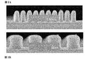
いくつかのこのような実施形態では、酸化アンチモン層は、ALDによって、パターン形成されたレジストの上にわたって共形的に堆積される。例が図1に図示されており、この図では、1つのSb2O3層が、構造化されたフォトレジストの上に100℃で堆積された。In some such embodiments, the antimony oxide layer is conformally deposited over the patterned resist by ALD. An example is illustrated in FIG. 1, where one Sb2 O3 layer was deposited at 100 ° C. on a structured photoresist.
酸化アンチモンは、犠牲層またはエッチング停止層として使用することができる。上で触れたように、SbOx膜とSiO2およびALDによって堆積されたAl2O3などの他の材料との間で、エッチング特性に差がある。例えば、Sb(OEt)3およびO3から堆積されたSb2O3膜は、1% HF、25% H2SO4、濃HNO3または2M NaOHを用いてエッチングすることはできなかった。しかしながら、この膜は、濃HCl中では約10nm/分の速度でエッチングすることができた。従って、いくつかの実施形態では、Sb(OEt)3およびO3から堆積されたSb2O3膜は、HClを使用して選択的にエッチングすることができ、または1% HF、25% H2SO4、濃HNO3または2M NaOHを使用して、異なる膜を、当該Sb2O3膜よりも選択的にエッチングすることができる。Antimony oxide can be used as a sacrificial layer or an etch stop layer. As mentioned above, there are differences in etching properties between SbOx films and other materials such as Al2 O3 deposited by SiO2 and ALD. For example, Sb2 O3 films deposited from Sb (OEt)3 and O3 could not be etched using 1% HF, 25% H2 SO4 , concentrated HNO3 or 2M NaOH. However, this film could be etched in concentrated HCl at a rate of about 10 nm / min. Thus, in some embodiments, Sb2 O3 films deposited from Sb (OEt)3 and O3 can be selectively etched using HCl, or 1% HF, 25% H Different films can be selectively etched over the Sb2 O3 film using2 SO4 , concentrated HNO3 or 2M NaOH.
他方、から堆積されたSbCl3およびO3から選択されたSb2O3膜は、1% HF、25% H2SO4、濃HCl、または濃HNO3を用いてエッチングすることができなかった。従って、いくつかの実施形態では、これらの化合物のうちの1以上を使用してエッチングすることができる膜は、これらの前駆体から堆積されたSb2O3膜よりも選択的にエッチングすることができる。On the other hand, Sb2 O3 films selected from SbCl3 and O3 deposited from could not be etched with 1% HF, 25% H2 SO4 , concentrated HCl, or concentrated HNO3 . Thus, in some embodiments, films that can be etched using one or more of these compounds are more selectively etched than Sb2 O3 films deposited from these precursors. Can do.
加えて、熱的SiO2はHF溶液の中で約2.8nm/分の速度でエッチングされるのに対し、本願明細書に記載されるようにして堆積されたSbOx膜は、同じHF溶液の中で顕著なエッチングをまったく示さないということが見出された。従って、いくつかの実施形態では、HFは、このようなSbOx膜よりもSiO2を選択的にエッチングするために使用される。他方、SbOx膜は、H2O2を用いて、約1〜2nm/分の速度でエッチングすることができたが、熱的SiO2はH2O2を用いてはエッチングされない。従って、他の実施形態では、このようなSbOx膜は、H2O2を使用して、熱的SiO2よりも選択的にエッチングすることができる。In addition, thermal SiO2 is etched in the HF solution at a rate of about 2.8 nm / min, whereas the SbOx film deposited as described herein is the same HF solution. Was found to show no significant etching. Thus, in some embodiments, HF is used to selectively etch SiO2 over such SbOx films. On the other hand, SbOx films could be etched with H2 O2 at a rate of about 1-2 nm / min, whereas thermal SiO2 was not etched with H2 O2 . Thus, in other embodiments, such SbOx films can be etched more selectively than thermal SiO2 using H2 O2 .
SbOx膜は、Al2O3膜、例えばALDによって堆積されたAl2O3膜に対して良好なエッチング選択性をも有する。H3PO4、HF、KOHおよびTMAHは、ALDによって堆積されたAl2O3膜をエッチングすることが見出されたが、SbOxをエッチングしなかったのに対し、Al2O3はH2O2、酒石酸または濃HClによってエッチングされなかった。従って、SbOxは、H2O2、酒石酸または濃HClを使用してAl2O3よりも選択的にエッチングすることができるのに対し、Al2O3は、H3PO4、HF、KOHまたはTMAHを使用してSbOxよりも選択的にエッチングすることができる。SbOx film has also a good etch selectivity tothe Al 2O 3 film, for example,Al 2O 3 films deposited by ALD. H3 PO4 , HF, KOH and TMAH were found to etch Al2 O3 films deposited by ALD, but did not etch SbOx , whereas Al2 O3 was H Not etched by2 O2 , tartaric acid or concentrated HCl. Thus, SbOx can be selectively etched over Al2 O3 using H2 O2 , tartaric acid or concentrated HCl, whereas Al2 O3 is H3 PO4 , HF, KOH or TMAH can be used to etch more selectively than SbOx .
いくつかの実施形態では、パターン形成されたレジスト層の上にわたって堆積された後、酸化アンチモン層はエッチングされて、下に存在するレジストが露出される。次いで、このレジストは取り除かれ、下に存在する基板がエッチングされて、所望の特徴部が形成される。 In some embodiments, after being deposited over the patterned resist layer, the antimony oxide layer is etched to expose the underlying resist. The resist is then removed and the underlying substrate is etched to form the desired features.
一般に、堆積が当該堆積枠の外にない限り、すなわち良好な品質を得るのに十分高いが、前駆体(複数可)の主要な分解を防ぐのに十分低い、従って膜の低品質、例えば、分解に起因する不純物を防止する温度にある限り、SbOx膜についての堆積温度が高いほど、それらは、高い耐エッチング性を有する。In general, unless the deposition is outside the deposition frame, i.e. high enough to obtain good quality, but low enough to prevent major degradation of the precursor (s), thus low quality of the film, e.g. The higher the deposition temperature for the SbOx film, the higher the resistance to etching as long as it is at a temperature that prevents impurities due to decomposition.
いくつかの実施形態では、SbOx膜は、SiO2およびSiの膜または層よりも選択的にエッチングすることができる。エッチングは、気相中でまたは「湿式エッチング」として液相中で実施されてもよい。エッチングを選択的に実施することができる例示的な選択的なエッチング溶液としては、濃HCl、H2O2および酒石酸が挙げられる。選択性は、好ましくは75%(1:3のエッチング速度差)超、80%(1:5のエッチング速度差)超、90%(1:10のエッチング速度差)超であり、ある場合には選択性は、95%(1:20のエッチング速度差)超、またはさらには98%(エッチング速度差1:50)超であることができる。いくつかの実施形態では、エッチング速度差は、1:100(99%の選択性)またはさらにはこれより高いことができる。In some embodiments, SbOx films can be etched more selectively than SiO2 and Si films or layers. Etching may be performed in the gas phase or in the liquid phase as a “wet etch”. Exemplary selective etching solutions in which etching can be selectively performed include concentrated HCl, H2 O2 and tartaric acid. The selectivity is preferably more than 75% (1: 3 etching rate difference), more than 80% (1: 5 etching rate difference), more than 90% (1:10 etching rate difference), in some cases The selectivity can be greater than 95% (1:20 etch rate difference), or even greater than 98% (etch rate difference 1:50). In some embodiments, the etch rate difference can be 1: 100 (99% selectivity) or even higher.
いくつかの実施形態では、SiO2膜は、本願明細書に記載されるようにして堆積されたSbOxの膜または層よりも選択的にエッチングすることができる。エッチングは、気相中または「湿式エッチング」として液相中で実施されてもよい。エッチングを選択的に実施することができる例示的なエッチング溶液としては、0.5%または1.0%の希HFなどのHF含有溶液が挙げられる。選択性は、75%(1:3のエッチング速度差)超、80%(1:5のエッチング速度差)超、90%(1:10のエッチング速度差)超、ある場合には95%(1:20のエッチング速度差)超またはさらには98%(1:50のエッチング速度差)超であってもよい。いくつかの実施形態では、99%またはさらにはこれより高い選択性を得ることができる(例えば1:100のエッチング速度差)。In some embodiments, the SiO2 film can be etched more selectively than SbOx films or layers deposited as described herein. Etching may be performed in the gas phase or in the liquid phase as a “wet etch”. Exemplary etching solutions that can be selectively etched include HF-containing solutions such as 0.5% or 1.0% dilute HF. Selectivity is over 75% (1: 3 etch rate difference), over 80% (1: 5 etch rate difference), over 90% (1:10 etch rate difference), and in some cases 95% ( It may be greater than 1:20 etch rate difference) or even 98% (1:50 etch rate difference). In some embodiments, 99% or even higher selectivity can be obtained (eg, an etch rate difference of 1: 100).
いくつかの実施形態では、SbOx膜は、Al2O3の膜または層よりも選択的にエッチングすることができる。エッチングは、気相中または「湿式エッチング」として液相中で実施されてもよい。例示的な選択的なエッチング溶液としては、濃HCl、H2O2および酒石酸が挙げられる。選択性は、75%(1:3のエッチング速度差)超、80%(1:5のエッチング速度差)超、90%(1:10のエッチング速度差)超、またはさらには95%(1:20のエッチング速度差)超または98%(1:50のエッチング速度差)超であってもよい。ある場合には、この選択性は、1:100のエッチング速度差以上を有して、99%以上であることができる。In some embodiments, the SbOx film can be etched more selectively than the Al2 O3 film or layer. Etching may be performed in the gas phase or in the liquid phase as a “wet etch”. Exemplary selective etching solutions include concentrated HCl, H2 O2 and tartaric acid. Selectivity is greater than 75% (1: 3 etch rate difference), greater than 80% (1: 5 etch rate difference), greater than 90% (1:10 etch rate difference), or even 95% (1 : Etching rate difference of 20) or more than 98% (etching rate difference of 1:50). In some cases, this selectivity can be greater than 99% with an etch rate difference greater than 1: 100.
いくつかの実施形態では、Al2O3膜は、本願明細書に記載されるようにして堆積されたSbOxの膜または層よりも選択的にエッチングすることができる。エッチングは、気相中または「湿式エッチング」として液相中で実施されてもよい。例示的な選択的なエッチング溶液としては、H3PO4、HF、KOHおよびTMAHが挙げられる。選択性は、75%(1:3のエッチング速度差)超、80%(1:5のエッチング速度差)超、90%(1:10のエッチング速度差)超、およびある場合には95%(1:20のエッチング速度差)超または98%(1:50のエッチング速度差)超であってもよい。ある場合には99%以上の選択性を、1:100のエッチング速度差以上を有して、成し遂げることができる。In some embodiments, the Al2 O3 film can be etched more selectively than SbOx films or layers deposited as described herein. Etching may be performed in the gas phase or in the liquid phase as a “wet etch”. Exemplary selective etching solutions include H3 PO4 , HF, KOH, and TMAH. Selectivities are over 75% (1: 3 etch rate difference), 80% (1: 5 etch rate difference), 90% (1:10 etch rate difference), and in some cases 95% It may be more than (1:20 etching rate difference) or more than 98% (1:50 etching rate difference). In some cases, selectivity of 99% or higher can be achieved with an etch rate difference of 1: 100 or higher.
いくつかの実施形態では、ケイ素または窒化ケイ素は、本願明細書に記載されるALDによって堆積されたSbOx膜よりも選択的にエッチングされる。これらの場合には、ケイ素または窒化ケイ素は、一般的なケイ素または窒化ケイ素のエッチング剤(腐食剤)を使用して、SbOxよりもエッチングすることができる。SbOxを、ケイ素または窒化ケイ素よりも選択的にエッチングすることもできる。例えば、濃HCl、H2O2または酒石酸を使用することができる。いくつかの実施形態では、選択性は、75%(1:3のエッチング速度差)超、80%(1:5のエッチング速度差)超、90%(1:10のエッチング速度差)、およびさらには95%(1:20のエッチング速度差)超または98%(1:50のエッチング速度差)超である。ある場合には、99%以上の選択性が、1:100のエッチング速度差またはさらにはこれより大きい速度差を有して、成し遂げられる。In some embodiments, silicon or silicon nitride is selectively etched over SbOx films deposited by ALD as described herein. In these cases, silicon or silicon nitride can be etched more than SbOx using common silicon or silicon nitride etchants (corrosives). SbOx can also be etched more selectively than silicon or silicon nitride. For example, concentrated HCl, H2 O2 or tartaric acid can be used. In some embodiments, the selectivity is greater than 75% (1: 3 etch rate difference), greater than 80% (1: 5 etch rate difference), 90% (1:10 etch rate difference), and Furthermore, it exceeds 95% (1:20 etching rate difference) or 98% (1:50 etching rate difference). In some cases, over 99% selectivity is achieved with an etch rate difference of 1: 100 or even greater.
いくつかの実施形態では、当該SbOx膜は、異なる材料に対してエッチング選択性を有する、または逆も言える − この他の物質は、SbOxに勝って選択的にエッチングすることができる。これらの場合、他の物質は、一般に公知のエッチング剤を使用して、SbOxよりも選択的にエッチングすることができる。また、SbOxは、濃HCl、H2O2または酒石酸を使用して、この他の物質よりも選択的にエッチングすることもできる。選択性は、75%(1:3のエッチング速度差)超、80%(1:5のエッチング速度差)超、90%(1:10のエッチング速度差)超、およびある場合には95%(1:20のエッチング速度差)超または98%(1:50のエッチング速度差)超であってもよい。ある場合には、選択性は、1:100のエッチング速度差以上を有して、99%以上であることができる。In some embodiments, the SbOx film has etch selectivity for different materials, or vice versa—this other material can be selectively etched over SbOx . In these cases, other materials can be etched more selectively than SbOx using generally known etchants. SbOx can also be etched more selectively than other materials using concentrated HCl, H2 O2 or tartaric acid. Selectivities are over 75% (1: 3 etch rate difference), 80% (1: 5 etch rate difference), 90% (1:10 etch rate difference), and in some cases 95% It may be more than (1:20 etching rate difference) or more than 98% (1:50 etching rate difference). In some cases, the selectivity can be 99% or more, with an etch rate difference of 1: 100 or more.
いくつかの実施形態では、当該SbOx膜は、乾式エッチング剤を使用して、SiNまたはSiO2などの他の物質に勝って選択的にエッチングすることができる。例えば、Clおよび/またはF含有プラズマエッチング剤を使用することができる。いくつかの実施形態では、Cl2プラズマまたはCHF3およびCl2プラズマの混合物が使用される。ここでも、選択性は、50%(1:2のエッチング速度差)超、75%(1:3のエッチング速度差)超、またはさらには90%(1:10のエッチング速度差)超であってもよい。In some embodiments, the SbOx film can be selectively etched over other materials such as SiN or SiO2 using a dry etchant. For example, Cl and / or F-containing plasma etchants can be used. In some embodiments, Cl2 plasma or a mixture of CHF3 and Cl2 plasma is used. Again, the selectivity was greater than 50% (1: 2 etch rate difference), greater than 75% (1: 3 etch rate difference), or even greater than 90% (1:10 etch rate difference). May be.
いくつかの実施形態では、例えば複数のパターニングプロセスにおいて基板上に構造体を形成する方法は、第1の物質を含む第1の膜を堆積することと、酸化アンチモンを含む第2の膜を堆積することとを含む。この酸化アンチモンは、例えば、基板を、アンチモン反応物質、例えばハロゲン化アンチモン、アンチモンアルコキシドまたはアンチモンアルキルアミン、および酸素ソース(例えばオゾン)に交互にかつ逐次的に接触させることにより、本願明細書に記載されるALDプロセスによって堆積される。その後、この第1の膜は、酸化アンチモンよりも選択的にエッチングされてもよいし、またはこの酸化アンチモンは、第1の膜よりも選択的にエッチングされてもよい。いくつかの実施形態では、この第1の物質は、例えば、SiO2またはAl2O3であってもよい。酸化アンチモンの第2の層が第1の層よりもエッチングされるとき、エッチングは、当該酸化アンチモン層を、濃HCl、H2O2および酒石酸からなる群から選択されるエッチング剤と接触させることを含んでもよい。当該酸化アンチモン層よりも第1の物質がエッチングされるとき、エッチングは、第1の物質を、HF、H3PO4、KOHおよびTMAHからなる群から選択されるエッチング剤と接触させることを含んでもよい。In some embodiments, for example, a method of forming a structure on a substrate in a plurality of patterning processes includes depositing a first film that includes a first material and a second film that includes antimony oxide. Including. The antimony oxide is described herein, for example, by contacting the substrate alternately and sequentially with an antimony reactant, such as antimony halide, antimony alkoxide or antimony alkylamine, and an oxygen source (eg, ozone). Deposited by an ALD process. Thereafter, the first film may be selectively etched over the antimony oxide, or the antimony oxide may be selectively etched over the first film. In some embodiments, this first material may be, for example, SiO2 or Al2 O3 . When the second layer of antimony oxide is etched more than the first layer, the etching contacts the antimony oxide layer with an etchant selected from the group consisting of concentrated HCl, H2 O2 and tartaric acid. May be included. When the first material is etched away from the antimony oxide layer, the etching includes contacting the first material with an etchant selected from the group consisting of HF, H3 PO4 , KOH and TMAH. But you can.
いくつかの実施形態では、酸化アンチモン薄膜は、アンチモンアルコキシドおよび酸素ソース(例えばオゾン)の交互かつ逐次的なパルスを含むALDサイクルを使用して堆積される。このアンチモンアルコキシドは、例えば、Sb(OEt)3であってもよい。この膜はバッチ反応器の中で堆積されてもよく、例えば、犠牲層としてまたはエッチング停止層として使用されてもよい。In some embodiments, the antimony oxide thin film is deposited using an ALD cycle that includes alternating and sequential pulses of antimony alkoxide and an oxygen source (eg, ozone). This antimony alkoxide may be, for example, Sb (OEt)3 . This film may be deposited in a batch reactor and used, for example, as a sacrificial layer or as an etch stop layer.
いくつかの実施形態では、酸化アンチモン薄膜は、アンチモンアルキルアミンおよび酸素ソース(例えばオゾン)の交互かつ逐次的なパルスを含むALDサイクルによって堆積される。この膜は、バッチ反応器の中で堆積されてもよく、例えば、犠牲層としてまたはエッチング停止層として使用されてもよい。 In some embodiments, the antimony oxide thin film is deposited by an ALD cycle that includes alternating and sequential pulses of antimony alkylamine and an oxygen source (eg, ozone). This film may be deposited in a batch reactor, for example, used as a sacrificial layer or as an etch stop layer.
実施例1 − シングルウェーハ反応器におけるアンチモンソースとしてのSb(OEt)3
酸化アンチモン(Sb2O3)薄膜を、Sb(OC2H5)3をアンチモンソースとして、およびO3を酸素ソースとして使用して、F−450 ALCVD(商標)反応器の中で、原子層堆積(ALD)によって堆積した。Example 1-Sb (OEt)3 as an antimony source in a single wafer reactor
Antimony oxide (Sb2 O3 ) thin film, atomic layer in F-450 ALCVD ™ reactor using Sb (OC2 H5 )3 as antimony source and O3 as oxygen source Deposited by deposition (ALD).
300℃でSb(OC2H5)3(パルス3.0秒間、パージ5.0秒間)およびH2O(パルス1.5秒間、パージ5.0秒間)を使用しても膜は得られなかったが、400℃ではいくらかの膜が得られた(成長速度約0.02Å/サイクル)。No film was obtained using Sb (OC2 H 5) 3 (pulse 3.0 seconds, purge 5.0 seconds) and H2 O (pulse 1.5 seconds, purge 5.0 seconds) at 300 ° C. At 400 ° C., some film was obtained (growth rate about 0.02 cm / cycle).
100〜350℃でSb(OC2H5)3およびO3の交互かつ逐次的なパルスを使用して膜を堆積した。Sb(OEt)3を3.0秒間パルス供与し、5.0秒間パージした。O3も3.0秒間パルス供与し、5.0秒間パージした。Sb(OC2H5)3は、室温(21℃)で使用した。Films were deposited using alternating and sequential pulses of Sb (OC2 H5 )3 and O3 at 100-350 ° C. Sb (OEt)3 was pulsed for 3.0 seconds and purged for 5.0 seconds. O3 was also pulsed for 3.0 seconds and purged for 5.0 seconds. Sb (OC2 H5 )3 was used at room temperature (21 ° C.).
成長速度は、約0.4〜1.3Å/サイクルの範囲であった。成長速度は、100〜250℃で0.4〜0.6Å/サイクルであり、275〜350℃では0.8Å/サイクル超であった。膜不均一性は、100〜150℃および350℃まででは高かった(>10% 1σ)。200〜300℃では、1σ不均一性は6%未満であり、275℃で最低の約3%であった。図2A〜図2Cは、100〜350℃における膜成長速度および不均一性を示す。 The growth rate was in the range of about 0.4 to 1.3 kg / cycle. The growth rate was 0.4 to 0.6 Å / cycle at 100 to 250 ° C, and more than 0.8 Å / cycle at 275 to 350 ° C. Film non-uniformity was high from 100 to 150 ° C. and up to 350 ° C. (> 10% 1σ). At 200-300 ° C, the 1σ inhomogeneity was less than 6%, with a minimum of about 3% at 275 ° C. 2A-2C show the film growth rate and non-uniformity at 100-350 ° C.
この膜を、X線反射(XRR)、X線回折(XRD)およびX線光電子分光法(XPS)、エネルギー分散型x線分析(EDX)および原子間力顕微鏡法(AFM)を用いて特性解析した。XRRによれば、膜密度は約6〜6.5g/cm3であり、密度は高い温度(200〜300℃)ほど大きくなった。XRRから得たrms粗さは、約1.4nm(200〜300℃で24〜40nm)であった。Sb2O3に帰属することができる非常に弱いピークが、150℃で堆積した試料のXRD回折図で見られた。AFM rms粗さは、約0.31nm(100℃で堆積された約25nm膜)であった。この膜は滑らかで均一であり、相イメージ(図3)において、コントラストは見られなかった。Characterization of this film using X-ray reflection (XRR), X-ray diffraction (XRD) and X-ray photoelectron spectroscopy (XPS), energy dispersive x-ray analysis (EDX) and atomic force microscopy (AFM) did. According to XRR, the film density was about 6 to 6.5 g / cm3 , and the density increased with higher temperature (200 to 300 ° C.). The rms roughness obtained from XRR was about 1.4 nm (24-40 nm at 200-300 ° C.). A very weak peak that could be attributed to Sb2 O3 was seen in the XRD diffractogram of the sample deposited at 150 ° C. The AFM rms roughness was about 0.31 nm (about 25 nm film deposited at 100 ° C.). The film was smooth and uniform and no contrast was seen in the phase image (FIG. 3).
XPSによれば(表1)、アンチモンの酸化状態は+3である。従って、この膜はSb2O3であった。炭素および窒素を、表面上の混入物質として検出したが、約5nmをスパッタリングした後は、何も検出できなかった。酸素濃度は、O1sおよびSb3d5のピークの重なりのため、およその値であった。O/Sbの減少(表2)は、高質量のSbよりも低質量の酸素の優先的スパッタリングに起因すると考えられる。XPS試料を250℃で堆積した。EDXは、300℃で堆積した膜の中で炭素を検出したが、塩素は検出しなかった。According to XPS (Table 1), the oxidation state of antimony is +3. Therefore, this film was Sb2 O3 . Carbon and nitrogen were detected as contaminants on the surface, but nothing could be detected after sputtering about 5 nm. The oxygen concentration was approximate due to the overlap of O1s and Sb3d5 peaks. The decrease in O / Sb (Table 2) is believed to be due to preferential sputtering of low mass oxygen over high mass Sb. XPS samples were deposited at 250 ° C. EDX detected carbon in the film deposited at 300 ° C., but not chlorine.
エッチング試験を、1% HF、25% H2SO4、2M NaOH、濃HNO3および濃HClの中で、室温で行った。当該膜は、濃HClでのみエッチングすることができた(エッチング速度約10nm/分)。1% HF、37% HClおよび0.5M 酒石酸を使用してさらなるエッチング試験を実施した。結果を下記の表2に示す。Etch tests were performed at room temperature in 1% HF, 25% H2 SO4 , 2M NaOH, concentrated HNO3 and concentrated HCl. The film could only be etched with concentrated HCl (etching rate about 10 nm / min). Further etching tests were performed using 1% HF, 37% HCl and 0.5M tartaric acid. The results are shown in Table 2 below.
表1。XPS結果。250℃で堆積したSb2O3膜。数字は原子%を呈示する。約5nmのスパッタリングの前(上段)および後(下段)に測定した。
図1に図示するように、構造化されたフォトレジストの上に100℃でSb2O3層を堆積した。30nmという厚さの目標値を選び、この堆積プロセスは750サイクルを含んでいた。各サイクルでは、Sb(OEt)3を3.5秒間パルス供与し、5.0秒間パージし、O3を3.0秒間パルス供与し、5秒間パージした。観察された段差被覆は95%超であった。約16というk値を観察した。As illustrated in FIG. 1, a Sb2 O3 layer was deposited at 100 ° C. on the structured photoresist. A target value of 30 nm thickness was chosen and the deposition process included 750 cycles. In each cycle, Sb (OEt)3 was pulsed for 3.5 seconds, purged for 5.0 seconds, and O3 was pulsed for 3.0 seconds and purged for 5 seconds. The step coverage observed was greater than 95%. A k value of about 16 was observed.
表2。反応物質としてのSb(OEt)3およびO3ならびに約100〜約200℃の反応温度を使用して堆積したSb2O3膜のエッチング結果
実施例2 − シングルウェーハ反応器におけるアンチモンソースとしてのSbCl3
酸化アンチモン(Sb2O3)薄膜を、SbCl3をアンチモンソースとして、およびO3を酸素ソースとして使用して、F−450 ALCVD(商標)反応器の中で、原子層堆積(ALD)によって堆積した。H2Oを酸素ソースとして使用すると(SbCl3パルス2.0秒間、パージ5.0秒間;H2Oパルス1.5秒間、パージ5秒間)、膜は得られなかった。しかしながら、O3に加えてH2Oを使用することにより、成長を高めることができ、均一性を増大させることができる。堆積サイクルは、SbCl3パルス2.0秒間、パージ5秒間;O3パルス3.0秒間、パージ5秒間;H2Oパルス1.5秒間、パージ5.0秒間からなっていた。Example 2 - SbCl3 as antimony source in a single wafer reactor
Antimony oxide (Sb2 O3 ) thin film deposited by atomic layer deposition (ALD) in an F-450 ALCVD ™ reactor using SbCl3 as an antimony source and O3 as an oxygen source did. When H2 O was used as the oxygen source (SbCl 3 pulse 2.0 seconds, purge 5.0 seconds; H 2 O pulse 1.5 seconds, purge 5 seconds), no film was obtained. However, the use of H2 O in addition to O3 can increase growth and increase uniformity. The deposition cycle consisted of SbCl3 pulse 2.0 seconds, purge 5 seconds; O3 pulse 3.0 seconds, purge 5 seconds; H2O pulse 1.5 seconds, purge 5.0 seconds.
各ALDサイクルでは、SbCl3を2秒間パルス供与し、5秒間パージし、他方でオゾンを3秒間パルス供与し、5秒間パージした。 In each ALD cycle, SbCl3 was pulsed for 2 seconds and purged for 5 seconds, while ozone was pulsed for 3 seconds and purged for 5 seconds.
膜を150〜400℃で堆積した。SbCl3についての気化温度は35℃であった。成長速度は0.3Å/サイクル未満であった。250℃未満の温度で、成長速度は<0.1Å/サイクルであった。300℃より上では、成長速度は0.2Å/サイクルであった。最高の成長速度は400℃での0.28Å/サイクルであった。The film was deposited at 150-400 ° C. The vaporization temperature for SbCl3 was 35 ° C. The growth rate was less than 0.3 kg / cycle. At temperatures below 250 ° C., the growth rate was <0.1 kg / cycle. Above 300 ° C., the growth rate was 0.2 kg / cycle. The highest growth rate was 0.28 Å / cycle at 400 ° C.
膜不均一性は約6〜約16%であった。不均一性は、低い堆積温度(150〜200℃)および最高温度の400℃では高かった(>10% 1σ)。250〜350℃では、1σ不均一性は5〜7%であった。 The film non-uniformity was about 6 to about 16%. The non-uniformity was high (> 10% 1σ) at the low deposition temperature (150-200 ° C.) and the maximum temperature of 400 ° C. At 250 to 350 ° C., the 1σ nonuniformity was 5 to 7%.
図4は、150〜400℃における膜成長速度および不均一性を示す。表3は、O3パルスの前後でのH2Oパルスの追加が成長速度および不均一性にどのように影響を及ぼすかを提示する。FIG. 4 shows the film growth rate and non-uniformity at 150-400 ° C. Table 3 presents how the addition of H2 O pulses before and after the O3 pulse affects growth rate and non-uniformity.
表3。成長速度および膜均一性に対するO3パルスの前後の追加的なH2Oパルスの効果
X線反射(XRR)、X線回折(XRD)およびX線光電子分光法(XPS)およびエネルギー分散型x線分析(EDX)を用いて膜を特性解析した。XRRによれば、膜密度は、約6〜6.6g/cm3であり、密度は、高い温度に向かって(150〜400℃)増大した。XRRから得たrms粗さは、1.3nm(150℃において6nm)、1.0(300℃において20nm)および400℃において1.2nmであった。400℃で堆積した試料に関しては、XRD回折図において明確なピークが観察されなかった。従って、この膜は非晶質であると推定された。XPS(表4)によれば、アンチモンの酸化状態は+3であり、従って、この膜はSb2O3であった。表面上の混入物質として炭素および窒素を検出したが、約5nmをスパッタリングした後は、いずれも検出できなかった。酸素濃度は、O1sおよびSb3d5のピークピークの重なりのため、およその値であった。O/Sbの減少(表4)は、高質量のSbよりも低質量の酸素の優先的スパッタリングに起因すると考えられる。XPS試料を400℃で堆積した。EDXは、400℃で堆積した膜では、炭素も塩素も検出しなかった。Films were characterized using X-ray reflection (XRR), X-ray diffraction (XRD) and X-ray photoelectron spectroscopy (XPS) and energy dispersive x-ray analysis (EDX). According to XRR, the film density was about 6-6.6 g / cm3 and the density increased towards higher temperatures (150-400 ° C.). The rms roughness obtained from XRR was 1.3 nm (6 nm at 150 ° C.), 1.0 (20 nm at 300 ° C.) and 1.2 nm at 400 ° C. For the sample deposited at 400 ° C., no clear peak was observed in the XRD diffractogram. Therefore, this film was estimated to be amorphous. According to XPS (Table 4), the oxidation state of antimony was +3, so this film was Sb2 O3 . Carbon and nitrogen were detected as contaminants on the surface, but none could be detected after sputtering about 5 nm. The oxygen concentration was approximate due to the overlap of the O1s and Sb3d5 peak peaks. The decrease in O / Sb (Table 4) is believed to be due to preferential sputtering of low mass oxygen over high mass Sb. XPS samples were deposited at 400 ° C. EDX detected no carbon or chlorine in films deposited at 400 ° C.
エッチング試験を、1% HF、25% H2SO4、濃HNO3および濃HClの中で、室温で行った。当該膜は、これらの溶液のいずれの中でもエッチングすることはできなかった(初期の膜厚が約40nmで1〜6分間のエッチング時間)。Etch tests were performed at room temperature in 1% HF, 25% H2 SO4 , concentrated HNO3 and concentrated HCl. The film could not be etched in any of these solutions (an initial film thickness of about 40 nm and an etch time of 1-6 minutes).
表4。XPS結果。400℃で堆積したSb2O3膜。数字は原子%を表す。
約5nmのスパッタリングの前(上段)および後(下段)に測定した。
It was measured before (upper) and after (lower) about 5 nm sputtering.
実施例3 − シングルウェーハ反応器におけるアンチモンソースとしてのSb(N(CH3)2)3
酸化アンチモン(SbOx)薄膜を、Sb(N(CH3)2)3をアンチモンソースとして、およびO3を酸素ソースとして使用して、Pulsar(登録商標) 2000 R&D反応器の中で、原子層堆積(ALD)によって堆積した。Example3 - Sb (N (CH 3 ) 2) as the antimony source in a single wafer reactor3
Antimony oxide (SbOx ) thin films, atomic layers in a Pulsar® 2000 R & D reactor using Sb (N (CH3 )2 )3 as an antimony source and O3 as an oxygen source Deposited by deposition (ALD).
Sb(N(CH3)2)3およびO3(O2中)の交互かつ逐次的なパルスを使用して、約100〜300℃の反応温度で、膜を堆積した。Sb(N(CH3)2)3を0.1〜1.0秒間パルス供与し、10秒間パージした。O3を10秒間パルス供与し、10秒間パージし、O3濃度は250g/m3(NTP)であった。Sb(N(CH3)2)3を室温(約20℃〜約23℃)で使用した。キャリアガスフローは0.8slmであった。Films were deposited at reaction temperatures of about 100-300 ° C. using alternating and sequential pulses of Sb (N (CH3 )2 )3 and O3 (in O2 ). Sb (N (CH3 )2 )3 was pulsed for 0.1-1.0 seconds and purged for 10 seconds. O3 was pulsed for 10 seconds, purged for 10 seconds, and the O3 concentration was 250 g / m3 (NTP). Sb (N (CH3 )2 )3 was used at room temperature (about 20 ° C. to about 23 ° C.). The carrier gas flow was 0.8 slm.
成長速度は、約0.83〜1.92Å/サイクルの範囲であった。成長速度は、約100℃では約1.44〜1.92Å/サイクルであり、200℃では約0.83〜約1.39Å/サイクルであった。膜不均一性(ウェーハ内)は、約2.1%〜約7.1%(1σ)にわたっていた。例えば、100℃で、およびSb(N(CH3)2)3パルス1秒間、パージ10秒間およびO3パルス10秒間、パージ10秒間、濃度250g/m3(NTP)を用いて堆積した500サイクルの膜は、1.92Å/サイクルの成長速度および2.1%(1σ)のウェーハ内均一性を有していた。図5および図6は、Sb(N(CH3)2)3+O3を用いた典型的なSbOx膜の特徴を提示する。The growth rate ranged from about 0.83 to 1.92 liters / cycle. The growth rate was about 1.44 to 1.92 Å / cycle at about 100 ° C and about 0.83 to about 1.39 Å / cycle at 200 ° C. Film non-uniformity (in-wafer) ranged from about 2.1% to about 7.1% (1σ). For example, 500 cycles deposited at 100 ° C. and using Sb (N (CH3 )2 )3 pulses for 1 second, purge 10 seconds and O3 pulse 10 seconds, purge 10 seconds, concentration 250 g / m3 (NTP) The film had a growth rate of 1.92 Å / cycle and an in-wafer uniformity of 2.1% (1σ). 5 and 6 present the characteristics of a typical SbOx film using Sb (N (CH3 )2 )3 + O3 .
実施例4 − バッチ反応器におけるアンチモンソースとしてのSb(OEt)3
酸化アンチモン(SbOx)薄膜を、Sb(OC2H5)3をアンチモンソースとしておよびO3を酸素ソースとして使用して、市販の、生産型のASM A412(商標) バッチ反応器の中で、原子層堆積(ALD)によって堆積した。Example 4-Sb (OEt)3 as antimony source in a batch reactor
In a commercial, production-type ASM A412 ™ batch reactor using antimony oxide (SbOx ) thin film, using Sb (OC2 H5 )3 as an antimony source and O3 as an oxygen source, Deposited by atomic layer deposition (ALD).
Sb(OC2H5)3およびO3の交互かつ逐次的なパルスを使用して、約140〜220℃の反応温度で、膜を堆積した。Sb(OEt)3を15〜40g/hrの投入量で3.0〜20秒間パルス供与し、10〜60秒間パージした。O3も、3.0〜20秒間パルス供与し、10〜600秒間パージした。Sb(OC2H5)3は、120℃で、液体注入システムで使用した。キャリアガスフローは約0.5slm〜約0.8slmにわたっていた。シングルピッチおよびダブルッピッチの両方のウェーハ投入を使用した。これらは、それぞれ、100製品または50製品のウェーハ容量に対応する。Films were deposited using alternating and sequential pulses of Sb (OC2 H5)3 and O3 at a reaction temperature of about 140-220 ° C. Sb (OEt)3 was pulsed for 3.0-20 seconds at an input rate of 15-40 g / hr and purged for 10-60 seconds. O3 was also pulsed for 3.0-20 seconds and purged for 10-600 seconds. Sb (OC2 H5 )3 was used at 120 ° C. in the liquid injection system. The carrier gas flow ranged from about 0.5 slm to about 0.8 slm. Both single-pitch and double-pitch wafer inputs were used. These correspond to a wafer capacity of 100 products or 50 products, respectively.
成長速度は、約0.38〜0.8Å/サイクルの範囲であった。成長速度は、約140℃では約0.38〜0.41Å/サイクルであり、200〜220℃では約0.5〜約0.8Å/サイクルであった。膜不均一性(ウェーハ内)は約3.4%〜約13%(1σ)にわたっており、ウェーハ間均一性は約0.1%〜約3.9%(1σ)にわたっていた。例えば、200℃でダブルピッチ投入量を用い、かつSb(OEt)3パルス5秒間、投入量25g/h、パージ10秒間およびO3パルス5秒間、パージ600秒間、濃度350g/m3を用いて堆積した200サイクルの膜は、0.63Å/サイクルの成長速度、3.4%(1σ)のウェーハ内均一性および0.39%(1σ)のウェーハ間均一性を有していた。The growth rate was in the range of about 0.38 to 0.8 kg / cycle. The growth rate was about 0.38 to 0.41 kg / cycle at about 140 ° C. and about 0.5 to about 0.8 kg / cycle at 200 to 220 ° C. Film non-uniformity (in-wafer) ranged from about 3.4% to about 13% (1σ) and wafer-to-wafer uniformity ranged from about 0.1% to about 3.9% (1σ). For example, using double pitch input at 200 ° C., Sb (OEt)3 pulses for 5 seconds, input 25 g / h, purge 10 seconds and O3 pulse 5 seconds, purge 600 seconds, concentration 350 g / m3 The deposited 200-cycle film had a growth rate of 0.63 Å / cycle, 3.4% (1σ) in-wafer uniformity and 0.39% (1σ) wafer-to-wafer uniformity.
実施例5 − シングルウェーハ反応器におけるアンチモンソースとしてのSb(OEt)3
酸化アンチモン(SbOx)薄膜を、Sb(OC2H5)3をアンチモンソースとしておよびO3を酸素ソースとして使用して、Pulsar(登録商標) 2000 R&D反応器の中で、原子層堆積(ALD)によって堆積した。Example 5-Sb (OEt)3 as an antimony source in a single wafer reactor
Antimony oxide (SbOx ) thin films were deposited in an atomic layer deposition (ALD) in a Pulsar® 2000 R & D reactor using Sb (OC2 H5 )3 as an antimony source and O3 as an oxygen source. ).
約200℃の反応温度で、Sb(OC2H5)3およびO3の交互かつ逐次的なパルスを使用して、膜を堆積した。Sb(OEt)3パルスを0.5秒に固定し、パージを10秒に固定した。O3を2.5〜30秒間パルス供与し、10秒間パージし、O3濃度は60〜300g/m3(NTP)であり、反応器へのO3フローは200〜800cm3/分(NTP)であった。Sb(OC2H5)3は40℃に加熱した。キャリアガスフローは0.8slmであった。Films were deposited using alternating and sequential pulses of Sb (OC2 H5)3 and O3 at a reaction temperature of about 200 ° C. Sb (OEt)3 pulses were fixed at 0.5 seconds and purge was fixed at 10 seconds. O3 was pulsed for 2.5-30 seconds, purged for 10 seconds, O3 concentration was 60-300 g / m3 (NTP), and O3 flow to the reactor was 200-800 cm3 / min (NTP )Met. Sb (OC2 H5 )3 was heated to 40 ° C. The carrier gas flow was 0.8 slm.
成長速度は約0.3〜0.7Å/サイクルの範囲であった。成長速度は、図7に示すように、使用したO3投入量に大きく依存し、図7では、菱形は、反応器の中のO3フローが変動した実施を表し、正方形は、O3濃度が変動した実施を表し、三角形は、O3パルス時間が変動した実施を表す。膜不均一性(ウェーハ内)は、約2.7%〜約49.5%(1σ)にわたっていた。より高いO3投入量は、膜のより高い成長速度を生じた。The growth rate was in the range of about 0.3-0.7 kg / cycle. The growth rate is highly dependent on the O3 input used, as shown in FIG. 7, where in FIG. 7 the diamonds represent implementations with varying O3 flow in the reactor, and the squares represent the O3 concentration. Represents an implementation with varying, and the triangle represents an implementation with varying O3 pulse time. Film non-uniformity (in-wafer) ranged from about 2.7% to about 49.5% (1σ). A higher O3 input resulted in a higher growth rate of the film.
実施例6 − バッチ反応器におけるアンチモンソースとしてのSb(N(CH3)2)3
酸化アンチモン(SbOx)薄膜を、Sb(N(CH3)2)3をアンチモンソースとして、およびO3を酸素ソースとして使用して、市販の、生産型のASM A412(商標) バッチ反応器の中で、原子層堆積(ALD)によって堆積した。Example6 - Sb (N (CH 3 ) 2) as the antimony source in a batch reactor3
A commercially available ASM A412 ™ batch reactor using antimony oxide (SbOx ) thin film, Sb (N (CH3 )2 )3 as antimony source, and O3 as oxygen source. In, deposited by atomic layer deposition (ALD).
Sb(N(CH3)2)3およびO3の交互かつ逐次的なパルスを使用して、約200℃の反応温度で、膜を堆積した。Sb(N(CH3)2)3を50g/hrの投入量で5.0秒間パルス供与し、120秒間パージした。O3も、350g/m3の濃度で5.0秒間パルス供与し、120秒間パージした。Sb(N(CH3)2)3は、120℃で、液体注入システムで使用した。キャリアガスフローは0.5slmであった。The film was deposited using an alternating and sequential pulse of Sb (N (CH3 )2 )3 and O3 at a reaction temperature of about 200 ° C. Sb (N (CH3 )2 )3 was pulsed for 5.0 seconds at a dosage of 50 g / hr and purged for 120 seconds. O3 was also pulsed at a concentration of 350 g / m3 for 5.0 seconds and purged for 120 seconds. Sb (N (CH3 )2 )3 was used in a liquid injection system at 120 ° C. The carrier gas flow was 0.5 slm.
SbOxの成長速度は約1.3〜1.4Å/サイクルの範囲であった。膜不均一性(ウェーハ内)は、約4.5%〜約5.3%(1σ)にわたっていた。4.5%膜厚不均一性地図は、図8で見ることができる。The growth rate of SbOx was in the range of about 1.3 to 1.4 Å / cycle. Film non-uniformity (in-wafer) ranged from about 4.5% to about 5.3% (1σ). A 4.5% film thickness non-uniformity map can be seen in FIG.
Claims (22)
Translated fromJapaneseバッチ反応器の中で、基板を、式SbRxA3−x(式中、xは1〜3であり、Rは、独立して選択される、直鎖状、分枝状、もしくは環状の、飽和もしくは不飽和の、C1−C12のアルキルまたはアルケニル基であり、Aは、アルキルアミン、ハライド、アミン、シリルまたはアルキルを含むリガンドである)を有するアンチモン前駆体と接触させることと、
過剰のアンチモン前駆体を除去することと、
前記基板をオゾンと接触させることと、
過剰のオゾンを除去することと
を含む、方法。A method of depositing an antimony oxide layer by atomic layer deposition, comprising:
In the batch reactor, the substrate is of the formula SbRx A3-x where x is 1 to 3 and R is independently selected, linear, branched, or cyclic. Contacting with an antimony precursor having a saturated or unsaturated C1-C12 alkyl or alkenyl group, wherein A is a ligand comprising an alkylamine, halide, amine, silyl or alkyl);
Removing excess antimony precursor;
Contacting the substrate with ozone;
Removing excess ozone.
第1の物質を含む第1の層を前記基板上に堆積することと、
酸化アンチモンの第2の層を、原子層堆積プロセスによって前記基板上に堆積することであって、前記原子層堆積プロセスは、前記基板をアンチモン前駆体および酸素ソースと交互にかつ逐次的に接触させることを含む、ことと、
前記第1の層および第2の層を同時にエッチャントにさらすことで、前記第1の層または第2の層のうち一方を、他方に対して選択的にエッチングすることと
を含み、
前記アンチモン前駆体は、式SbRxA3−x(式中、xは1〜3であり、Rは、独立して選択される、直鎖状、分枝状、もしくは環状の、飽和もしくは不飽和の、C1−C12のアルキルまたはアルケニル基であり、Aは、アルキルアミン、ハライド、アミン、シリルまたはアルキルを含むリガンドである)を有する、方法。A method of forming a structure on a semiconductor substrate in a reaction space,
Depositing a first layer comprising a first material on the substrate;
Depositing a second layer of antimony oxide on the substrate by an atomic layer deposition process, wherein the atomic layer deposition process contacts the substrate alternately and sequentially with an antimony precursor and an oxygen source. Including that, and
Selectively etching one of the first layer or the second layerwithrespect tothe other by exposing the first layer and the second layer to an etchant simultaneously,
The antimony precursor has the formula SbRx A3-x , where x is 1 to 3 and R is independently selected, linear, branched, or cyclic, saturated or unsaturated. A saturated, C1-C12 alkyl or alkenyl group, wherein A is a ligand comprising an alkylamine, halide, amine, silyl or alkyl).
Applications Claiming Priority (4)
| Application Number | Priority Date | Filing Date | Title |
|---|---|---|---|
| US201161546500P | 2011-10-12 | 2011-10-12 | |
| US61/546,500 | 2011-10-12 | ||
| US201261597373P | 2012-02-10 | 2012-02-10 | |
| US61/597,373 | 2012-02-10 |
Related Child Applications (1)
| Application Number | Title | Priority Date | Filing Date |
|---|---|---|---|
| JP2017143477ADivisionJP2018021259A (en) | 2011-10-12 | 2017-07-25 | Atomic layer deposition of antimony oxide film |
Publications (3)
| Publication Number | Publication Date |
|---|---|
| JP2013084959A JP2013084959A (en) | 2013-05-09 |
| JP2013084959A5 JP2013084959A5 (en) | 2015-12-10 |
| JP6202798B2true JP6202798B2 (en) | 2017-09-27 |
Family
ID=48086285
Family Applications (2)
| Application Number | Title | Priority Date | Filing Date |
|---|---|---|---|
| JP2012225541AActiveJP6202798B2 (en) | 2011-10-12 | 2012-10-10 | Atomic layer deposition of antimony oxide films. |
| JP2017143477APendingJP2018021259A (en) | 2011-10-12 | 2017-07-25 | Atomic layer deposition of antimony oxide film |
Family Applications After (1)
| Application Number | Title | Priority Date | Filing Date |
|---|---|---|---|
| JP2017143477APendingJP2018021259A (en) | 2011-10-12 | 2017-07-25 | Atomic layer deposition of antimony oxide film |
Country Status (3)
| Country | Link |
|---|---|
| US (4) | US9006112B2 (en) |
| JP (2) | JP6202798B2 (en) |
| KR (2) | KR20130039699A (en) |
Families Citing this family (398)
| Publication number | Priority date | Publication date | Assignee | Title |
|---|---|---|---|---|
| US10378106B2 (en) | 2008-11-14 | 2019-08-13 | Asm Ip Holding B.V. | Method of forming insulation film by modified PEALD |
| US9394608B2 (en) | 2009-04-06 | 2016-07-19 | Asm America, Inc. | Semiconductor processing reactor and components thereof |
| US8802201B2 (en) | 2009-08-14 | 2014-08-12 | Asm America, Inc. | Systems and methods for thin-film deposition of metal oxides using excited nitrogen-oxygen species |
| TWI529808B (en) | 2010-06-10 | 2016-04-11 | Asm國際股份有限公司 | Method for selectively depositing film on substrate |
| US9312155B2 (en) | 2011-06-06 | 2016-04-12 | Asm Japan K.K. | High-throughput semiconductor-processing apparatus equipped with multiple dual-chamber modules |
| US10364496B2 (en) | 2011-06-27 | 2019-07-30 | Asm Ip Holding B.V. | Dual section module having shared and unshared mass flow controllers |
| US10854498B2 (en) | 2011-07-15 | 2020-12-01 | Asm Ip Holding B.V. | Wafer-supporting device and method for producing same |
| US20130023129A1 (en) | 2011-07-20 | 2013-01-24 | Asm America, Inc. | Pressure transmitter for a semiconductor processing environment |
| JP6202798B2 (en)* | 2011-10-12 | 2017-09-27 | エーエスエム インターナショナル エヌ.ヴェー.Asm International N.V. | Atomic layer deposition of antimony oxide films. |
| US9017481B1 (en) | 2011-10-28 | 2015-04-28 | Asm America, Inc. | Process feed management for semiconductor substrate processing |
| US9112003B2 (en) | 2011-12-09 | 2015-08-18 | Asm International N.V. | Selective formation of metallic films on metallic surfaces |
| US9023427B2 (en)* | 2012-05-16 | 2015-05-05 | Asm Ip Holding B.V. | Methods for forming multi-component thin films |
| US9659799B2 (en) | 2012-08-28 | 2017-05-23 | Asm Ip Holding B.V. | Systems and methods for dynamic semiconductor process scheduling |
| US9021985B2 (en) | 2012-09-12 | 2015-05-05 | Asm Ip Holdings B.V. | Process gas management for an inductively-coupled plasma deposition reactor |
| US10714315B2 (en) | 2012-10-12 | 2020-07-14 | Asm Ip Holdings B.V. | Semiconductor reaction chamber showerhead |
| US20160376700A1 (en) | 2013-02-01 | 2016-12-29 | Asm Ip Holding B.V. | System for treatment of deposition reactor |
| US9589770B2 (en) | 2013-03-08 | 2017-03-07 | Asm Ip Holding B.V. | Method and systems for in-situ formation of intermediate reactive species |
| US9484191B2 (en) | 2013-03-08 | 2016-11-01 | Asm Ip Holding B.V. | Pulsed remote plasma method and system |
| US9564309B2 (en)* | 2013-03-14 | 2017-02-07 | Asm Ip Holding B.V. | Si precursors for deposition of SiN at low temperatures |
| US9824881B2 (en) | 2013-03-14 | 2017-11-21 | Asm Ip Holding B.V. | Si precursors for deposition of SiN at low temperatures |
| US9240412B2 (en) | 2013-09-27 | 2016-01-19 | Asm Ip Holding B.V. | Semiconductor structure and device and methods of forming same using selective epitaxial process |
| US9362109B2 (en)* | 2013-10-16 | 2016-06-07 | Asm Ip Holding B.V. | Deposition of boron and carbon containing materials |
| US9401273B2 (en) | 2013-12-11 | 2016-07-26 | Asm Ip Holding B.V. | Atomic layer deposition of silicon carbon nitride based materials |
| US9895715B2 (en) | 2014-02-04 | 2018-02-20 | Asm Ip Holding B.V. | Selective deposition of metals, metal oxides, and dielectrics |
| US10683571B2 (en) | 2014-02-25 | 2020-06-16 | Asm Ip Holding B.V. | Gas supply manifold and method of supplying gases to chamber using same |
| US10167557B2 (en) | 2014-03-18 | 2019-01-01 | Asm Ip Holding B.V. | Gas distribution system, reactor including the system, and methods of using the same |
| US11015245B2 (en) | 2014-03-19 | 2021-05-25 | Asm Ip Holding B.V. | Gas-phase reactor and system having exhaust plenum and components thereof |
| US10047435B2 (en) | 2014-04-16 | 2018-08-14 | Asm Ip Holding B.V. | Dual selective deposition |
| US10858737B2 (en) | 2014-07-28 | 2020-12-08 | Asm Ip Holding B.V. | Showerhead assembly and components thereof |
| US9890456B2 (en) | 2014-08-21 | 2018-02-13 | Asm Ip Holding B.V. | Method and system for in situ formation of gas-phase compounds |
| US9576792B2 (en) | 2014-09-17 | 2017-02-21 | Asm Ip Holding B.V. | Deposition of SiN |
| US9657845B2 (en) | 2014-10-07 | 2017-05-23 | Asm Ip Holding B.V. | Variable conductance gas distribution apparatus and method |
| US10941490B2 (en) | 2014-10-07 | 2021-03-09 | Asm Ip Holding B.V. | Multiple temperature range susceptor, assembly, reactor and system including the susceptor, and methods of using the same |
| EP3224657B1 (en)* | 2014-11-26 | 2024-04-10 | Jaiswal, Supriya | Materials, components, and methods for use with extreme ultraviolet radiation in lithography and other applications |
| KR102263121B1 (en) | 2014-12-22 | 2021-06-09 | 에이에스엠 아이피 홀딩 비.브이. | Semiconductor device and manufacuring method thereof |
| US9816180B2 (en) | 2015-02-03 | 2017-11-14 | Asm Ip Holding B.V. | Selective deposition |
| US9490145B2 (en) | 2015-02-23 | 2016-11-08 | Asm Ip Holding B.V. | Removal of surface passivation |
| US10529542B2 (en) | 2015-03-11 | 2020-01-07 | Asm Ip Holdings B.V. | Cross-flow reactor and method |
| US10276355B2 (en) | 2015-03-12 | 2019-04-30 | Asm Ip Holding B.V. | Multi-zone reactor, system including the reactor, and method of using the same |
| US10458018B2 (en) | 2015-06-26 | 2019-10-29 | Asm Ip Holding B.V. | Structures including metal carbide material, devices including the structures, and methods of forming same |
| US10600673B2 (en) | 2015-07-07 | 2020-03-24 | Asm Ip Holding B.V. | Magnetic susceptor to baseplate seal |
| US10083836B2 (en) | 2015-07-24 | 2018-09-25 | Asm Ip Holding B.V. | Formation of boron-doped titanium metal films with high work function |
| US10428421B2 (en) | 2015-08-03 | 2019-10-01 | Asm Ip Holding B.V. | Selective deposition on metal or metallic surfaces relative to dielectric surfaces |
| US10121699B2 (en) | 2015-08-05 | 2018-11-06 | Asm Ip Holding B.V. | Selective deposition of aluminum and nitrogen containing material |
| US10566185B2 (en) | 2015-08-05 | 2020-02-18 | Asm Ip Holding B.V. | Selective deposition of aluminum and nitrogen containing material |
| US10410857B2 (en) | 2015-08-24 | 2019-09-10 | Asm Ip Holding B.V. | Formation of SiN thin films |
| US9960072B2 (en) | 2015-09-29 | 2018-05-01 | Asm Ip Holding B.V. | Variable adjustment for precise matching of multiple chamber cavity housings |
| US10695794B2 (en) | 2015-10-09 | 2020-06-30 | Asm Ip Holding B.V. | Vapor phase deposition of organic films |
| US10814349B2 (en) | 2015-10-09 | 2020-10-27 | Asm Ip Holding B.V. | Vapor phase deposition of organic films |
| US10343186B2 (en) | 2015-10-09 | 2019-07-09 | Asm Ip Holding B.V. | Vapor phase deposition of organic films |
| US10211308B2 (en) | 2015-10-21 | 2019-02-19 | Asm Ip Holding B.V. | NbMC layers |
| US10322384B2 (en) | 2015-11-09 | 2019-06-18 | Asm Ip Holding B.V. | Counter flow mixer for process chamber |
| US11139308B2 (en) | 2015-12-29 | 2021-10-05 | Asm Ip Holding B.V. | Atomic layer deposition of III-V compounds to form V-NAND devices |
| US10468251B2 (en) | 2016-02-19 | 2019-11-05 | Asm Ip Holding B.V. | Method for forming spacers using silicon nitride film for spacer-defined multiple patterning |
| US10529554B2 (en) | 2016-02-19 | 2020-01-07 | Asm Ip Holding B.V. | Method for forming silicon nitride film selectively on sidewalls or flat surfaces of trenches |
| US9981286B2 (en) | 2016-03-08 | 2018-05-29 | Asm Ip Holding B.V. | Selective formation of metal silicides |
| US10501866B2 (en) | 2016-03-09 | 2019-12-10 | Asm Ip Holding B.V. | Gas distribution apparatus for improved film uniformity in an epitaxial system |
| US10343920B2 (en) | 2016-03-18 | 2019-07-09 | Asm Ip Holding B.V. | Aligned carbon nanotubes |
| US9892913B2 (en) | 2016-03-24 | 2018-02-13 | Asm Ip Holding B.V. | Radial and thickness control via biased multi-port injection settings |
| US10204782B2 (en) | 2016-04-18 | 2019-02-12 | Imec Vzw | Combined anneal and selective deposition process |
| WO2017184357A1 (en) | 2016-04-18 | 2017-10-26 | Asm Ip Holding B.V. | Method of forming a directed self-assembled layer on a substrate |
| US10865475B2 (en) | 2016-04-21 | 2020-12-15 | Asm Ip Holding B.V. | Deposition of metal borides and silicides |
| US10190213B2 (en) | 2016-04-21 | 2019-01-29 | Asm Ip Holding B.V. | Deposition of metal borides |
| US10032628B2 (en) | 2016-05-02 | 2018-07-24 | Asm Ip Holding B.V. | Source/drain performance through conformal solid state doping |
| US10367080B2 (en) | 2016-05-02 | 2019-07-30 | Asm Ip Holding B.V. | Method of forming a germanium oxynitride film |
| US11081342B2 (en) | 2016-05-05 | 2021-08-03 | Asm Ip Holding B.V. | Selective deposition using hydrophobic precursors |
| KR102592471B1 (en) | 2016-05-17 | 2023-10-20 | 에이에스엠 아이피 홀딩 비.브이. | Method of forming metal interconnection and method of fabricating semiconductor device using the same |
| US11453943B2 (en) | 2016-05-25 | 2022-09-27 | Asm Ip Holding B.V. | Method for forming carbon-containing silicon/metal oxide or nitride film by ALD using silicon precursor and hydrocarbon precursor |
| US10373820B2 (en) | 2016-06-01 | 2019-08-06 | Asm Ip Holding B.V. | Deposition of organic films |
| US10453701B2 (en) | 2016-06-01 | 2019-10-22 | Asm Ip Holding B.V. | Deposition of organic films |
| US10014212B2 (en) | 2016-06-08 | 2018-07-03 | Asm Ip Holding B.V. | Selective deposition of metallic films |
| US9803277B1 (en) | 2016-06-08 | 2017-10-31 | Asm Ip Holding B.V. | Reaction chamber passivation and selective deposition of metallic films |
| US10388509B2 (en) | 2016-06-28 | 2019-08-20 | Asm Ip Holding B.V. | Formation of epitaxial layers via dislocation filtering |
| US10612137B2 (en) | 2016-07-08 | 2020-04-07 | Asm Ip Holdings B.V. | Organic reactants for atomic layer deposition |
| US9859151B1 (en) | 2016-07-08 | 2018-01-02 | Asm Ip Holding B.V. | Selective film deposition method to form air gaps |
| US10714385B2 (en) | 2016-07-19 | 2020-07-14 | Asm Ip Holding B.V. | Selective deposition of tungsten |
| US10381226B2 (en) | 2016-07-27 | 2019-08-13 | Asm Ip Holding B.V. | Method of processing substrate |
| US9887082B1 (en) | 2016-07-28 | 2018-02-06 | Asm Ip Holding B.V. | Method and apparatus for filling a gap |
| US9812320B1 (en) | 2016-07-28 | 2017-11-07 | Asm Ip Holding B.V. | Method and apparatus for filling a gap |
| US10395919B2 (en) | 2016-07-28 | 2019-08-27 | Asm Ip Holding B.V. | Method and apparatus for filling a gap |
| KR102532607B1 (en) | 2016-07-28 | 2023-05-15 | 에이에스엠 아이피 홀딩 비.브이. | Substrate processing apparatus and method of operating the same |
| US10410943B2 (en) | 2016-10-13 | 2019-09-10 | Asm Ip Holding B.V. | Method for passivating a surface of a semiconductor and related systems |
| US10643826B2 (en) | 2016-10-26 | 2020-05-05 | Asm Ip Holdings B.V. | Methods for thermally calibrating reaction chambers |
| US11532757B2 (en) | 2016-10-27 | 2022-12-20 | Asm Ip Holding B.V. | Deposition of charge trapping layers |
| US10643904B2 (en) | 2016-11-01 | 2020-05-05 | Asm Ip Holdings B.V. | Methods for forming a semiconductor device and related semiconductor device structures |
| US10435790B2 (en) | 2016-11-01 | 2019-10-08 | Asm Ip Holding B.V. | Method of subatmospheric plasma-enhanced ALD using capacitively coupled electrodes with narrow gap |
| US10229833B2 (en) | 2016-11-01 | 2019-03-12 | Asm Ip Holding B.V. | Methods for forming a transition metal nitride film on a substrate by atomic layer deposition and related semiconductor device structures |
| US10714350B2 (en) | 2016-11-01 | 2020-07-14 | ASM IP Holdings, B.V. | Methods for forming a transition metal niobium nitride film on a substrate by atomic layer deposition and related semiconductor device structures |
| US10134757B2 (en) | 2016-11-07 | 2018-11-20 | Asm Ip Holding B.V. | Method of processing a substrate and a device manufactured by using the method |
| KR102546317B1 (en) | 2016-11-15 | 2023-06-21 | 에이에스엠 아이피 홀딩 비.브이. | Gas supply unit and substrate processing apparatus including the same |
| US10340135B2 (en) | 2016-11-28 | 2019-07-02 | Asm Ip Holding B.V. | Method of topologically restricted plasma-enhanced cyclic deposition of silicon or metal nitride |
| US11430656B2 (en) | 2016-11-29 | 2022-08-30 | Asm Ip Holding B.V. | Deposition of oxide thin films |
| KR102762543B1 (en) | 2016-12-14 | 2025-02-05 | 에이에스엠 아이피 홀딩 비.브이. | Substrate processing apparatus |
| US11581186B2 (en) | 2016-12-15 | 2023-02-14 | Asm Ip Holding B.V. | Sequential infiltration synthesis apparatus |
| US11447861B2 (en) | 2016-12-15 | 2022-09-20 | Asm Ip Holding B.V. | Sequential infiltration synthesis apparatus and a method of forming a patterned structure |
| KR102700194B1 (en) | 2016-12-19 | 2024-08-28 | 에이에스엠 아이피 홀딩 비.브이. | Substrate processing apparatus |
| US10269558B2 (en) | 2016-12-22 | 2019-04-23 | Asm Ip Holding B.V. | Method of forming a structure on a substrate |
| US10867788B2 (en) | 2016-12-28 | 2020-12-15 | Asm Ip Holding B.V. | Method of forming a structure on a substrate |
| US11390950B2 (en) | 2017-01-10 | 2022-07-19 | Asm Ip Holding B.V. | Reactor system and method to reduce residue buildup during a film deposition process |
| US10655221B2 (en) | 2017-02-09 | 2020-05-19 | Asm Ip Holding B.V. | Method for depositing oxide film by thermal ALD and PEALD |
| JP7169072B2 (en) | 2017-02-14 | 2022-11-10 | エーエスエム アイピー ホールディング ビー.ブイ. | Selective passivation and selective deposition |
| US10468261B2 (en) | 2017-02-15 | 2019-11-05 | Asm Ip Holding B.V. | Methods for forming a metallic film on a substrate by cyclical deposition and related semiconductor device structures |
| US10529563B2 (en) | 2017-03-29 | 2020-01-07 | Asm Ip Holdings B.V. | Method for forming doped metal oxide films on a substrate by cyclical deposition and related semiconductor device structures |
| US10283353B2 (en) | 2017-03-29 | 2019-05-07 | Asm Ip Holding B.V. | Method of reforming insulating film deposited on substrate with recess pattern |
| KR102457289B1 (en) | 2017-04-25 | 2022-10-21 | 에이에스엠 아이피 홀딩 비.브이. | Method for depositing a thin film and manufacturing a semiconductor device |
| US11501965B2 (en) | 2017-05-05 | 2022-11-15 | Asm Ip Holding B.V. | Plasma enhanced deposition processes for controlled formation of metal oxide thin films |
| US10446393B2 (en) | 2017-05-08 | 2019-10-15 | Asm Ip Holding B.V. | Methods for forming silicon-containing epitaxial layers and related semiconductor device structures |
| US10770286B2 (en) | 2017-05-08 | 2020-09-08 | Asm Ip Holdings B.V. | Methods for selectively forming a silicon nitride film on a substrate and related semiconductor device structures |
| US10892156B2 (en) | 2017-05-08 | 2021-01-12 | Asm Ip Holding B.V. | Methods for forming a silicon nitride film on a substrate and related semiconductor device structures |
| JP7183187B2 (en) | 2017-05-16 | 2022-12-05 | エーエスエム アイピー ホールディング ビー.ブイ. | Selective PEALD of oxides on dielectrics |
| US10504742B2 (en) | 2017-05-31 | 2019-12-10 | Asm Ip Holding B.V. | Method of atomic layer etching using hydrogen plasma |
| US10886123B2 (en) | 2017-06-02 | 2021-01-05 | Asm Ip Holding B.V. | Methods for forming low temperature semiconductor layers and related semiconductor device structures |
| US12040200B2 (en) | 2017-06-20 | 2024-07-16 | Asm Ip Holding B.V. | Semiconductor processing apparatus and methods for calibrating a semiconductor processing apparatus |
| US11306395B2 (en) | 2017-06-28 | 2022-04-19 | Asm Ip Holding B.V. | Methods for depositing a transition metal nitride film on a substrate by atomic layer deposition and related deposition apparatus |
| US10685834B2 (en) | 2017-07-05 | 2020-06-16 | Asm Ip Holdings B.V. | Methods for forming a silicon germanium tin layer and related semiconductor device structures |
| US10900120B2 (en) | 2017-07-14 | 2021-01-26 | Asm Ip Holding B.V. | Passivation against vapor deposition |
| KR20190009245A (en) | 2017-07-18 | 2019-01-28 | 에이에스엠 아이피 홀딩 비.브이. | Methods for forming a semiconductor device structure and related semiconductor device structures |
| US11374112B2 (en) | 2017-07-19 | 2022-06-28 | Asm Ip Holding B.V. | Method for depositing a group IV semiconductor and related semiconductor device structures |
| US11018002B2 (en) | 2017-07-19 | 2021-05-25 | Asm Ip Holding B.V. | Method for selectively depositing a Group IV semiconductor and related semiconductor device structures |
| US10541333B2 (en) | 2017-07-19 | 2020-01-21 | Asm Ip Holding B.V. | Method for depositing a group IV semiconductor and related semiconductor device structures |
| US10312055B2 (en) | 2017-07-26 | 2019-06-04 | Asm Ip Holding B.V. | Method of depositing film by PEALD using negative bias |
| US10590535B2 (en) | 2017-07-26 | 2020-03-17 | Asm Ip Holdings B.V. | Chemical treatment, deposition and/or infiltration apparatus and method for using the same |
| US10605530B2 (en) | 2017-07-26 | 2020-03-31 | Asm Ip Holding B.V. | Assembly of a liner and a flange for a vertical furnace as well as the liner and the vertical furnace |
| TWI815813B (en) | 2017-08-04 | 2023-09-21 | 荷蘭商Asm智慧財產控股公司 | Showerhead assembly for distributing a gas within a reaction chamber |
| US10692741B2 (en) | 2017-08-08 | 2020-06-23 | Asm Ip Holdings B.V. | Radiation shield |
| US10770336B2 (en) | 2017-08-08 | 2020-09-08 | Asm Ip Holding B.V. | Substrate lift mechanism and reactor including same |
| US11139191B2 (en) | 2017-08-09 | 2021-10-05 | Asm Ip Holding B.V. | Storage apparatus for storing cassettes for substrates and processing apparatus equipped therewith |
| US11769682B2 (en) | 2017-08-09 | 2023-09-26 | Asm Ip Holding B.V. | Storage apparatus for storing cassettes for substrates and processing apparatus equipped therewith |
| US10249524B2 (en) | 2017-08-09 | 2019-04-02 | Asm Ip Holding B.V. | Cassette holder assembly for a substrate cassette and holding member for use in such assembly |
| US10236177B1 (en) | 2017-08-22 | 2019-03-19 | ASM IP Holding B.V.. | Methods for depositing a doped germanium tin semiconductor and related semiconductor device structures |
| USD900036S1 (en) | 2017-08-24 | 2020-10-27 | Asm Ip Holding B.V. | Heater electrical connector and adapter |
| US11830730B2 (en) | 2017-08-29 | 2023-11-28 | Asm Ip Holding B.V. | Layer forming method and apparatus |
| KR102491945B1 (en) | 2017-08-30 | 2023-01-26 | 에이에스엠 아이피 홀딩 비.브이. | Substrate processing apparatus |
| US11295980B2 (en) | 2017-08-30 | 2022-04-05 | Asm Ip Holding B.V. | Methods for depositing a molybdenum metal film over a dielectric surface of a substrate by a cyclical deposition process and related semiconductor device structures |
| US11056344B2 (en) | 2017-08-30 | 2021-07-06 | Asm Ip Holding B.V. | Layer forming method |
| KR102401446B1 (en) | 2017-08-31 | 2022-05-24 | 에이에스엠 아이피 홀딩 비.브이. | Substrate processing apparatus |
| US10607895B2 (en) | 2017-09-18 | 2020-03-31 | Asm Ip Holdings B.V. | Method for forming a semiconductor device structure comprising a gate fill metal |
| KR102630301B1 (en) | 2017-09-21 | 2024-01-29 | 에이에스엠 아이피 홀딩 비.브이. | Method of sequential infiltration synthesis treatment of infiltrateable material and structures and devices formed using same |
| US10844484B2 (en) | 2017-09-22 | 2020-11-24 | Asm Ip Holding B.V. | Apparatus for dispensing a vapor phase reactant to a reaction chamber and related methods |
| US10658205B2 (en) | 2017-09-28 | 2020-05-19 | Asm Ip Holdings B.V. | Chemical dispensing apparatus and methods for dispensing a chemical to a reaction chamber |
| US10403504B2 (en) | 2017-10-05 | 2019-09-03 | Asm Ip Holding B.V. | Method for selectively depositing a metallic film on a substrate |
| US10319588B2 (en) | 2017-10-10 | 2019-06-11 | Asm Ip Holding B.V. | Method for depositing a metal chalcogenide on a substrate by cyclical deposition |
| US10923344B2 (en) | 2017-10-30 | 2021-02-16 | Asm Ip Holding B.V. | Methods for forming a semiconductor structure and related semiconductor structures |
| KR102443047B1 (en) | 2017-11-16 | 2022-09-14 | 에이에스엠 아이피 홀딩 비.브이. | Method of processing a substrate and a device manufactured by the same |
| US10910262B2 (en) | 2017-11-16 | 2021-02-02 | Asm Ip Holding B.V. | Method of selectively depositing a capping layer structure on a semiconductor device structure |
| US11022879B2 (en) | 2017-11-24 | 2021-06-01 | Asm Ip Holding B.V. | Method of forming an enhanced unexposed photoresist layer |
| JP7214724B2 (en) | 2017-11-27 | 2023-01-30 | エーエスエム アイピー ホールディング ビー.ブイ. | Storage device for storing wafer cassettes used in batch furnaces |
| US11639811B2 (en) | 2017-11-27 | 2023-05-02 | Asm Ip Holding B.V. | Apparatus including a clean mini environment |
| US10290508B1 (en) | 2017-12-05 | 2019-05-14 | Asm Ip Holding B.V. | Method for forming vertical spacers for spacer-defined patterning |
| US10872771B2 (en) | 2018-01-16 | 2020-12-22 | Asm Ip Holding B. V. | Method for depositing a material film on a substrate within a reaction chamber by a cyclical deposition process and related device structures |
| TWI799494B (en) | 2018-01-19 | 2023-04-21 | 荷蘭商Asm 智慧財產控股公司 | Deposition method |
| US11482412B2 (en) | 2018-01-19 | 2022-10-25 | Asm Ip Holding B.V. | Method for depositing a gap-fill layer by plasma-assisted deposition |
| USD903477S1 (en) | 2018-01-24 | 2020-12-01 | Asm Ip Holdings B.V. | Metal clamp |
| US11018047B2 (en) | 2018-01-25 | 2021-05-25 | Asm Ip Holding B.V. | Hybrid lift pin |
| USD880437S1 (en) | 2018-02-01 | 2020-04-07 | Asm Ip Holding B.V. | Gas supply plate for semiconductor manufacturing apparatus |
| US10535516B2 (en) | 2018-02-01 | 2020-01-14 | Asm Ip Holdings B.V. | Method for depositing a semiconductor structure on a surface of a substrate and related semiconductor structures |
| US11081345B2 (en) | 2018-02-06 | 2021-08-03 | Asm Ip Holding B.V. | Method of post-deposition treatment for silicon oxide film |
| US10896820B2 (en) | 2018-02-14 | 2021-01-19 | Asm Ip Holding B.V. | Method for depositing a ruthenium-containing film on a substrate by a cyclical deposition process |
| KR102657269B1 (en) | 2018-02-14 | 2024-04-16 | 에이에스엠 아이피 홀딩 비.브이. | Method for depositing a ruthenium-containing film on a substrate by a cyclic deposition process |
| US10731249B2 (en) | 2018-02-15 | 2020-08-04 | Asm Ip Holding B.V. | Method of forming a transition metal containing film on a substrate by a cyclical deposition process, a method for supplying a transition metal halide compound to a reaction chamber, and related vapor deposition apparatus |
| US10658181B2 (en) | 2018-02-20 | 2020-05-19 | Asm Ip Holding B.V. | Method of spacer-defined direct patterning in semiconductor fabrication |
| KR102636427B1 (en) | 2018-02-20 | 2024-02-13 | 에이에스엠 아이피 홀딩 비.브이. | Substrate processing method and apparatus |
| US10975470B2 (en) | 2018-02-23 | 2021-04-13 | Asm Ip Holding B.V. | Apparatus for detecting or monitoring for a chemical precursor in a high temperature environment |
| US11473195B2 (en) | 2018-03-01 | 2022-10-18 | Asm Ip Holding B.V. | Semiconductor processing apparatus and a method for processing a substrate |
| US11629406B2 (en) | 2018-03-09 | 2023-04-18 | Asm Ip Holding B.V. | Semiconductor processing apparatus comprising one or more pyrometers for measuring a temperature of a substrate during transfer of the substrate |
| US11114283B2 (en) | 2018-03-16 | 2021-09-07 | Asm Ip Holding B.V. | Reactor, system including the reactor, and methods of manufacturing and using same |
| KR102646467B1 (en) | 2018-03-27 | 2024-03-11 | 에이에스엠 아이피 홀딩 비.브이. | Method of forming an electrode on a substrate and a semiconductor device structure including an electrode |
| US11230766B2 (en) | 2018-03-29 | 2022-01-25 | Asm Ip Holding B.V. | Substrate processing apparatus and method |
| US11088002B2 (en) | 2018-03-29 | 2021-08-10 | Asm Ip Holding B.V. | Substrate rack and a substrate processing system and method |
| US10510536B2 (en) | 2018-03-29 | 2019-12-17 | Asm Ip Holding B.V. | Method of depositing a co-doped polysilicon film on a surface of a substrate within a reaction chamber |
| KR102501472B1 (en) | 2018-03-30 | 2023-02-20 | 에이에스엠 아이피 홀딩 비.브이. | Substrate processing method |
| KR102600229B1 (en) | 2018-04-09 | 2023-11-10 | 에이에스엠 아이피 홀딩 비.브이. | Substrate supporting device, substrate processing apparatus including the same and substrate processing method |
| US10580645B2 (en) | 2018-04-30 | 2020-03-03 | Asm Ip Holding B.V. | Plasma enhanced atomic layer deposition (PEALD) of SiN using silicon-hydrohalide precursors |
| JP7146690B2 (en) | 2018-05-02 | 2022-10-04 | エーエスエム アイピー ホールディング ビー.ブイ. | Selective layer formation using deposition and removal |
| US12025484B2 (en) | 2018-05-08 | 2024-07-02 | Asm Ip Holding B.V. | Thin film forming method |
| TWI843623B (en) | 2018-05-08 | 2024-05-21 | 荷蘭商Asm Ip私人控股有限公司 | Methods for depositing an oxide film on a substrate by a cyclical deposition process and related device structures |
| US12272527B2 (en) | 2018-05-09 | 2025-04-08 | Asm Ip Holding B.V. | Apparatus for use with hydrogen radicals and method of using same |
| KR20190129718A (en) | 2018-05-11 | 2019-11-20 | 에이에스엠 아이피 홀딩 비.브이. | Methods for forming a doped metal carbide film on a substrate and related semiconductor device structures |
| KR102596988B1 (en) | 2018-05-28 | 2023-10-31 | 에이에스엠 아이피 홀딩 비.브이. | Method of processing a substrate and a device manufactured by the same |
| US11718913B2 (en) | 2018-06-04 | 2023-08-08 | Asm Ip Holding B.V. | Gas distribution system and reactor system including same |
| TWI840362B (en) | 2018-06-04 | 2024-05-01 | 荷蘭商Asm Ip私人控股有限公司 | Wafer handling chamber with moisture reduction |
| US11286562B2 (en) | 2018-06-08 | 2022-03-29 | Asm Ip Holding B.V. | Gas-phase chemical reactor and method of using same |
| KR102568797B1 (en) | 2018-06-21 | 2023-08-21 | 에이에스엠 아이피 홀딩 비.브이. | Substrate processing system |
| US10797133B2 (en) | 2018-06-21 | 2020-10-06 | Asm Ip Holding B.V. | Method for depositing a phosphorus doped silicon arsenide film and related semiconductor device structures |
| KR102854019B1 (en) | 2018-06-27 | 2025-09-02 | 에이에스엠 아이피 홀딩 비.브이. | Periodic deposition method for forming a metal-containing material and films and structures comprising the metal-containing material |
| TWI815915B (en) | 2018-06-27 | 2023-09-21 | 荷蘭商Asm Ip私人控股有限公司 | Cyclic deposition methods for forming metal-containing material and films and structures including the metal-containing material |
| US10612136B2 (en) | 2018-06-29 | 2020-04-07 | ASM IP Holding, B.V. | Temperature-controlled flange and reactor system including same |
| KR102686758B1 (en) | 2018-06-29 | 2024-07-18 | 에이에스엠 아이피 홀딩 비.브이. | Method for depositing a thin film and manufacturing a semiconductor device |
| US10755922B2 (en) | 2018-07-03 | 2020-08-25 | Asm Ip Holding B.V. | Method for depositing silicon-free carbon-containing film as gap-fill layer by pulse plasma-assisted deposition |
| US10388513B1 (en) | 2018-07-03 | 2019-08-20 | Asm Ip Holding B.V. | Method for depositing silicon-free carbon-containing film as gap-fill layer by pulse plasma-assisted deposition |
| US10767789B2 (en) | 2018-07-16 | 2020-09-08 | Asm Ip Holding B.V. | Diaphragm valves, valve components, and methods for forming valve components |
| US10483099B1 (en) | 2018-07-26 | 2019-11-19 | Asm Ip Holding B.V. | Method for forming thermally stable organosilicon polymer film |
| US11053591B2 (en) | 2018-08-06 | 2021-07-06 | Asm Ip Holding B.V. | Multi-port gas injection system and reactor system including same |
| US10883175B2 (en) | 2018-08-09 | 2021-01-05 | Asm Ip Holding B.V. | Vertical furnace for processing substrates and a liner for use therein |
| US10829852B2 (en) | 2018-08-16 | 2020-11-10 | Asm Ip Holding B.V. | Gas distribution device for a wafer processing apparatus |
| US11430674B2 (en) | 2018-08-22 | 2022-08-30 | Asm Ip Holding B.V. | Sensor array, apparatus for dispensing a vapor phase reactant to a reaction chamber and related methods |
| US11024523B2 (en) | 2018-09-11 | 2021-06-01 | Asm Ip Holding B.V. | Substrate processing apparatus and method |
| KR102707956B1 (en) | 2018-09-11 | 2024-09-19 | 에이에스엠 아이피 홀딩 비.브이. | Method for deposition of a thin film |
| US11049751B2 (en) | 2018-09-14 | 2021-06-29 | Asm Ip Holding B.V. | Cassette supply system to store and handle cassettes and processing apparatus equipped therewith |
| CN110970344B (en) | 2018-10-01 | 2024-10-25 | Asmip控股有限公司 | Substrate holding apparatus, system comprising the same and method of using the same |
| JP2020056104A (en) | 2018-10-02 | 2020-04-09 | エーエスエム アイピー ホールディング ビー.ブイ. | Selective passivation and selective deposition |
| US11232963B2 (en) | 2018-10-03 | 2022-01-25 | Asm Ip Holding B.V. | Substrate processing apparatus and method |
| KR102592699B1 (en) | 2018-10-08 | 2023-10-23 | 에이에스엠 아이피 홀딩 비.브이. | Substrate support unit and apparatuses for depositing thin film and processing the substrate including the same |
| US10847365B2 (en) | 2018-10-11 | 2020-11-24 | Asm Ip Holding B.V. | Method of forming conformal silicon carbide film by cyclic CVD |
| US10811256B2 (en) | 2018-10-16 | 2020-10-20 | Asm Ip Holding B.V. | Method for etching a carbon-containing feature |
| KR102605121B1 (en) | 2018-10-19 | 2023-11-23 | 에이에스엠 아이피 홀딩 비.브이. | Substrate processing apparatus and substrate processing method |
| KR102546322B1 (en) | 2018-10-19 | 2023-06-21 | 에이에스엠 아이피 홀딩 비.브이. | Substrate processing apparatus and substrate processing method |
| USD948463S1 (en) | 2018-10-24 | 2022-04-12 | Asm Ip Holding B.V. | Susceptor for semiconductor substrate supporting apparatus |
| US10381219B1 (en) | 2018-10-25 | 2019-08-13 | Asm Ip Holding B.V. | Methods for forming a silicon nitride film |
| US12378665B2 (en) | 2018-10-26 | 2025-08-05 | Asm Ip Holding B.V. | High temperature coatings for a preclean and etch apparatus and related methods |
| US11087997B2 (en) | 2018-10-31 | 2021-08-10 | Asm Ip Holding B.V. | Substrate processing apparatus for processing substrates |
| KR102748291B1 (en) | 2018-11-02 | 2024-12-31 | 에이에스엠 아이피 홀딩 비.브이. | Substrate support unit and substrate processing apparatus including the same |
| US11572620B2 (en) | 2018-11-06 | 2023-02-07 | Asm Ip Holding B.V. | Methods for selectively depositing an amorphous silicon film on a substrate |
| US11031242B2 (en) | 2018-11-07 | 2021-06-08 | Asm Ip Holding B.V. | Methods for depositing a boron doped silicon germanium film |
| US10847366B2 (en) | 2018-11-16 | 2020-11-24 | Asm Ip Holding B.V. | Methods for depositing a transition metal chalcogenide film on a substrate by a cyclical deposition process |
| US10818758B2 (en) | 2018-11-16 | 2020-10-27 | Asm Ip Holding B.V. | Methods for forming a metal silicate film on a substrate in a reaction chamber and related semiconductor device structures |
| US10559458B1 (en) | 2018-11-26 | 2020-02-11 | Asm Ip Holding B.V. | Method of forming oxynitride film |
| US12040199B2 (en) | 2018-11-28 | 2024-07-16 | Asm Ip Holding B.V. | Substrate processing apparatus for processing substrates |
| US11217444B2 (en)* | 2018-11-30 | 2022-01-04 | Asm Ip Holding B.V. | Method for forming an ultraviolet radiation responsive metal oxide-containing film |
| KR102636428B1 (en) | 2018-12-04 | 2024-02-13 | 에이에스엠 아이피 홀딩 비.브이. | A method for cleaning a substrate processing apparatus |
| US11158513B2 (en) | 2018-12-13 | 2021-10-26 | Asm Ip Holding B.V. | Methods for forming a rhenium-containing film on a substrate by a cyclical deposition process and related semiconductor device structures |
| JP7504584B2 (en) | 2018-12-14 | 2024-06-24 | エーエスエム・アイピー・ホールディング・ベー・フェー | Method and system for forming device structures using selective deposition of gallium nitride - Patents.com |
| TWI866480B (en) | 2019-01-17 | 2024-12-11 | 荷蘭商Asm Ip 私人控股有限公司 | Methods of forming a transition metal containing film on a substrate by a cyclical deposition process |
| KR102727227B1 (en) | 2019-01-22 | 2024-11-07 | 에이에스엠 아이피 홀딩 비.브이. | Semiconductor processing device |
| CN111524788B (en) | 2019-02-01 | 2023-11-24 | Asm Ip私人控股有限公司 | Method for forming topologically selective films of silicon oxide |
| US11482533B2 (en) | 2019-02-20 | 2022-10-25 | Asm Ip Holding B.V. | Apparatus and methods for plug fill deposition in 3-D NAND applications |
| JP7603377B2 (en) | 2019-02-20 | 2024-12-20 | エーエスエム・アイピー・ホールディング・ベー・フェー | Method and apparatus for filling recesses formed in a substrate surface - Patents.com |
| KR102626263B1 (en) | 2019-02-20 | 2024-01-16 | 에이에스엠 아이피 홀딩 비.브이. | Cyclical deposition method including treatment step and apparatus for same |
| TWI845607B (en) | 2019-02-20 | 2024-06-21 | 荷蘭商Asm Ip私人控股有限公司 | Cyclical deposition method and apparatus for filling a recess formed within a substrate surface |
| TWI842826B (en) | 2019-02-22 | 2024-05-21 | 荷蘭商Asm Ip私人控股有限公司 | Substrate processing apparatus and method for processing substrate |
| KR102858005B1 (en) | 2019-03-08 | 2025-09-09 | 에이에스엠 아이피 홀딩 비.브이. | Method for Selective Deposition of Silicon Nitride Layer and Structure Including Selectively-Deposited Silicon Nitride Layer |
| KR102782593B1 (en) | 2019-03-08 | 2025-03-14 | 에이에스엠 아이피 홀딩 비.브이. | Structure Including SiOC Layer and Method of Forming Same |
| US11742198B2 (en) | 2019-03-08 | 2023-08-29 | Asm Ip Holding B.V. | Structure including SiOCN layer and method of forming same |
| KR20200116033A (en) | 2019-03-28 | 2020-10-08 | 에이에스엠 아이피 홀딩 비.브이. | Door opener and substrate processing apparatus provided therewith |
| KR102809999B1 (en) | 2019-04-01 | 2025-05-19 | 에이에스엠 아이피 홀딩 비.브이. | Method of manufacturing semiconductor device |
| US11965238B2 (en) | 2019-04-12 | 2024-04-23 | Asm Ip Holding B.V. | Selective deposition of metal oxides on metal surfaces |
| KR20200123380A (en) | 2019-04-19 | 2020-10-29 | 에이에스엠 아이피 홀딩 비.브이. | Layer forming method and apparatus |
| KR20200125453A (en) | 2019-04-24 | 2020-11-04 | 에이에스엠 아이피 홀딩 비.브이. | Gas-phase reactor system and method of using same |
| US11289326B2 (en) | 2019-05-07 | 2022-03-29 | Asm Ip Holding B.V. | Method for reforming amorphous carbon polymer film |
| KR20200130121A (en) | 2019-05-07 | 2020-11-18 | 에이에스엠 아이피 홀딩 비.브이. | Chemical source vessel with dip tube |
| KR20200130652A (en) | 2019-05-10 | 2020-11-19 | 에이에스엠 아이피 홀딩 비.브이. | Method of depositing material onto a surface and structure formed according to the method |
| JP7612342B2 (en) | 2019-05-16 | 2025-01-14 | エーエスエム・アイピー・ホールディング・ベー・フェー | Wafer boat handling apparatus, vertical batch furnace and method |
| JP7598201B2 (en) | 2019-05-16 | 2024-12-11 | エーエスエム・アイピー・ホールディング・ベー・フェー | Wafer boat handling apparatus, vertical batch furnace and method |
| USD947913S1 (en) | 2019-05-17 | 2022-04-05 | Asm Ip Holding B.V. | Susceptor shaft |
| USD975665S1 (en) | 2019-05-17 | 2023-01-17 | Asm Ip Holding B.V. | Susceptor shaft |
| USD935572S1 (en) | 2019-05-24 | 2021-11-09 | Asm Ip Holding B.V. | Gas channel plate |
| USD922229S1 (en) | 2019-06-05 | 2021-06-15 | Asm Ip Holding B.V. | Device for controlling a temperature of a gas supply unit |
| KR20200141003A (en) | 2019-06-06 | 2020-12-17 | 에이에스엠 아이피 홀딩 비.브이. | Gas-phase reactor system including a gas detector |
| KR20200141931A (en) | 2019-06-10 | 2020-12-21 | 에이에스엠 아이피 홀딩 비.브이. | Method for cleaning quartz epitaxial chambers |
| KR20200143254A (en) | 2019-06-11 | 2020-12-23 | 에이에스엠 아이피 홀딩 비.브이. | Method of forming an electronic structure using an reforming gas, system for performing the method, and structure formed using the method |
| USD944946S1 (en) | 2019-06-14 | 2022-03-01 | Asm Ip Holding B.V. | Shower plate |
| USD931978S1 (en) | 2019-06-27 | 2021-09-28 | Asm Ip Holding B.V. | Showerhead vacuum transport |
| KR20210005515A (en) | 2019-07-03 | 2021-01-14 | 에이에스엠 아이피 홀딩 비.브이. | Temperature control assembly for substrate processing apparatus and method of using same |
| JP7499079B2 (en) | 2019-07-09 | 2024-06-13 | エーエスエム・アイピー・ホールディング・ベー・フェー | Plasma device using coaxial waveguide and substrate processing method |
| CN112216646A (en) | 2019-07-10 | 2021-01-12 | Asm Ip私人控股有限公司 | Substrate supporting assembly and substrate processing device comprising same |
| KR20210010307A (en) | 2019-07-16 | 2021-01-27 | 에이에스엠 아이피 홀딩 비.브이. | Substrate processing apparatus |
| KR20210010816A (en) | 2019-07-17 | 2021-01-28 | 에이에스엠 아이피 홀딩 비.브이. | Radical assist ignition plasma system and method |
| KR102860110B1 (en) | 2019-07-17 | 2025-09-16 | 에이에스엠 아이피 홀딩 비.브이. | Methods of forming silicon germanium structures |
| US11643724B2 (en) | 2019-07-18 | 2023-05-09 | Asm Ip Holding B.V. | Method of forming structures using a neutral beam |
| TWI839544B (en) | 2019-07-19 | 2024-04-21 | 荷蘭商Asm Ip私人控股有限公司 | Method of forming topology-controlled amorphous carbon polymer film |
| KR20210010817A (en) | 2019-07-19 | 2021-01-28 | 에이에스엠 아이피 홀딩 비.브이. | Method of Forming Topology-Controlled Amorphous Carbon Polymer Film |
| TWI851767B (en) | 2019-07-29 | 2024-08-11 | 荷蘭商Asm Ip私人控股有限公司 | Methods for selective deposition utilizing n-type dopants and/or alternative dopants to achieve high dopant incorporation |
| CN112309899A (en) | 2019-07-30 | 2021-02-02 | Asm Ip私人控股有限公司 | Substrate processing apparatus |
| CN112309900A (en) | 2019-07-30 | 2021-02-02 | Asm Ip私人控股有限公司 | Substrate processing apparatus |
| US12169361B2 (en) | 2019-07-30 | 2024-12-17 | Asm Ip Holding B.V. | Substrate processing apparatus and method |
| US11227782B2 (en) | 2019-07-31 | 2022-01-18 | Asm Ip Holding B.V. | Vertical batch furnace assembly |
| US11587814B2 (en) | 2019-07-31 | 2023-02-21 | Asm Ip Holding B.V. | Vertical batch furnace assembly |
| US11587815B2 (en) | 2019-07-31 | 2023-02-21 | Asm Ip Holding B.V. | Vertical batch furnace assembly |
| CN118422165A (en) | 2019-08-05 | 2024-08-02 | Asm Ip私人控股有限公司 | Liquid level sensor for chemical source container |
| CN112342526A (en) | 2019-08-09 | 2021-02-09 | Asm Ip私人控股有限公司 | Heater assembly including cooling device and method of using same |
| USD965044S1 (en) | 2019-08-19 | 2022-09-27 | Asm Ip Holding B.V. | Susceptor shaft |
| USD965524S1 (en) | 2019-08-19 | 2022-10-04 | Asm Ip Holding B.V. | Susceptor support |
| JP2021031769A (en) | 2019-08-21 | 2021-03-01 | エーエスエム アイピー ホールディング ビー.ブイ. | Production apparatus of mixed gas of film deposition raw material and film deposition apparatus |
| USD940837S1 (en) | 2019-08-22 | 2022-01-11 | Asm Ip Holding B.V. | Electrode |
| KR20210024423A (en) | 2019-08-22 | 2021-03-05 | 에이에스엠 아이피 홀딩 비.브이. | Method for forming a structure with a hole |
| USD930782S1 (en) | 2019-08-22 | 2021-09-14 | Asm Ip Holding B.V. | Gas distributor |
| USD979506S1 (en) | 2019-08-22 | 2023-02-28 | Asm Ip Holding B.V. | Insulator |
| USD949319S1 (en) | 2019-08-22 | 2022-04-19 | Asm Ip Holding B.V. | Exhaust duct |
| KR20210024420A (en) | 2019-08-23 | 2021-03-05 | 에이에스엠 아이피 홀딩 비.브이. | Method for depositing silicon oxide film having improved quality by peald using bis(diethylamino)silane |
| US11286558B2 (en) | 2019-08-23 | 2022-03-29 | Asm Ip Holding B.V. | Methods for depositing a molybdenum nitride film on a surface of a substrate by a cyclical deposition process and related semiconductor device structures including a molybdenum nitride film |
| KR102806450B1 (en) | 2019-09-04 | 2025-05-12 | 에이에스엠 아이피 홀딩 비.브이. | Methods for selective deposition using a sacrificial capping layer |
| KR102733104B1 (en) | 2019-09-05 | 2024-11-22 | 에이에스엠 아이피 홀딩 비.브이. | Substrate processing apparatus |
| US11562901B2 (en) | 2019-09-25 | 2023-01-24 | Asm Ip Holding B.V. | Substrate processing method |
| CN112593212B (en) | 2019-10-02 | 2023-12-22 | Asm Ip私人控股有限公司 | Method for forming topologically selective silicon oxide film by cyclic plasma enhanced deposition process |
| TWI846953B (en) | 2019-10-08 | 2024-07-01 | 荷蘭商Asm Ip私人控股有限公司 | Substrate processing device |
| KR20210042810A (en) | 2019-10-08 | 2021-04-20 | 에이에스엠 아이피 홀딩 비.브이. | Reactor system including a gas distribution assembly for use with activated species and method of using same |
| TW202128273A (en) | 2019-10-08 | 2021-08-01 | 荷蘭商Asm Ip私人控股有限公司 | Gas injection system, reactor system, and method of depositing material on surface of substratewithin reaction chamber |
| TWI846966B (en) | 2019-10-10 | 2024-07-01 | 荷蘭商Asm Ip私人控股有限公司 | Method of forming a photoresist underlayer and structure including same |
| US12009241B2 (en) | 2019-10-14 | 2024-06-11 | Asm Ip Holding B.V. | Vertical batch furnace assembly with detector to detect cassette |
| TWI834919B (en) | 2019-10-16 | 2024-03-11 | 荷蘭商Asm Ip私人控股有限公司 | Method of topology-selective film formation of silicon oxide |
| US11637014B2 (en) | 2019-10-17 | 2023-04-25 | Asm Ip Holding B.V. | Methods for selective deposition of doped semiconductor material |
| KR102845724B1 (en) | 2019-10-21 | 2025-08-13 | 에이에스엠 아이피 홀딩 비.브이. | Apparatus and methods for selectively etching films |
| KR20210050453A (en) | 2019-10-25 | 2021-05-07 | 에이에스엠 아이피 홀딩 비.브이. | Methods for filling a gap feature on a substrate surface and related semiconductor structures |
| US11646205B2 (en) | 2019-10-29 | 2023-05-09 | Asm Ip Holding B.V. | Methods of selectively forming n-type doped material on a surface, systems for selectively forming n-type doped material, and structures formed using same |
| US11139163B2 (en) | 2019-10-31 | 2021-10-05 | Asm Ip Holding B.V. | Selective deposition of SiOC thin films |
| KR20210054983A (en) | 2019-11-05 | 2021-05-14 | 에이에스엠 아이피 홀딩 비.브이. | Structures with doped semiconductor layers and methods and systems for forming same |
| US11501968B2 (en) | 2019-11-15 | 2022-11-15 | Asm Ip Holding B.V. | Method for providing a semiconductor device with silicon filled gaps |
| KR102861314B1 (en) | 2019-11-20 | 2025-09-17 | 에이에스엠 아이피 홀딩 비.브이. | Method of depositing carbon-containing material on a surface of a substrate, structure formed using the method, and system for forming the structure |
| CN112951697B (en) | 2019-11-26 | 2025-07-29 | Asmip私人控股有限公司 | Substrate processing apparatus |
| US11450529B2 (en) | 2019-11-26 | 2022-09-20 | Asm Ip Holding B.V. | Methods for selectively forming a target film on a substrate comprising a first dielectric surface and a second metallic surface |
| CN120432376A (en) | 2019-11-29 | 2025-08-05 | Asm Ip私人控股有限公司 | Substrate processing apparatus |
| CN112885692B (en) | 2019-11-29 | 2025-08-15 | Asmip私人控股有限公司 | Substrate processing apparatus |
| JP7527928B2 (en) | 2019-12-02 | 2024-08-05 | エーエスエム・アイピー・ホールディング・ベー・フェー | Substrate processing apparatus and substrate processing method |
| KR20210070898A (en) | 2019-12-04 | 2021-06-15 | 에이에스엠 아이피 홀딩 비.브이. | Substrate processing apparatus |
| CN112992667A (en) | 2019-12-17 | 2021-06-18 | Asm Ip私人控股有限公司 | Method of forming vanadium nitride layer and structure including vanadium nitride layer |
| US11527403B2 (en) | 2019-12-19 | 2022-12-13 | Asm Ip Holding B.V. | Methods for filling a gap feature on a substrate surface and related semiconductor structures |
| JP7636892B2 (en) | 2020-01-06 | 2025-02-27 | エーエスエム・アイピー・ホールディング・ベー・フェー | Channeled Lift Pins |
| TW202140135A (en) | 2020-01-06 | 2021-11-01 | 荷蘭商Asm Ip私人控股有限公司 | Gas supply assembly and valve plate assembly |
| US11993847B2 (en) | 2020-01-08 | 2024-05-28 | Asm Ip Holding B.V. | Injector |
| KR20210093163A (en) | 2020-01-16 | 2021-07-27 | 에이에스엠 아이피 홀딩 비.브이. | Method of forming high aspect ratio features |
| KR102675856B1 (en) | 2020-01-20 | 2024-06-17 | 에이에스엠 아이피 홀딩 비.브이. | Method of forming thin film and method of modifying surface of thin film |
| TWI889744B (en) | 2020-01-29 | 2025-07-11 | 荷蘭商Asm Ip私人控股有限公司 | Contaminant trap system, and baffle plate stack |
| TW202513845A (en) | 2020-02-03 | 2025-04-01 | 荷蘭商Asm Ip私人控股有限公司 | Semiconductor structures and methods for forming the same |
| TW202146882A (en) | 2020-02-04 | 2021-12-16 | 荷蘭商Asm Ip私人控股有限公司 | Method of verifying an article, apparatus for verifying an article, and system for verifying a reaction chamber |
| US11776846B2 (en) | 2020-02-07 | 2023-10-03 | Asm Ip Holding B.V. | Methods for depositing gap filling fluids and related systems and devices |
| KR20210103956A (en) | 2020-02-13 | 2021-08-24 | 에이에스엠 아이피 홀딩 비.브이. | Substrate processing apparatus including light receiving device and calibration method of light receiving device |
| KR20210103953A (en) | 2020-02-13 | 2021-08-24 | 에이에스엠 아이피 홀딩 비.브이. | Gas distribution assembly and method of using same |
| US11781243B2 (en) | 2020-02-17 | 2023-10-10 | Asm Ip Holding B.V. | Method for depositing low temperature phosphorous-doped silicon |
| CN113410160A (en) | 2020-02-28 | 2021-09-17 | Asm Ip私人控股有限公司 | System specially used for cleaning parts |
| KR20210113043A (en) | 2020-03-04 | 2021-09-15 | 에이에스엠 아이피 홀딩 비.브이. | Alignment fixture for a reactor system |
| KR20210116249A (en) | 2020-03-11 | 2021-09-27 | 에이에스엠 아이피 홀딩 비.브이. | lockout tagout assembly and system and method of using same |
| KR20210116240A (en) | 2020-03-11 | 2021-09-27 | 에이에스엠 아이피 홀딩 비.브이. | Substrate handling device with adjustable joints |
| KR102775390B1 (en) | 2020-03-12 | 2025-02-28 | 에이에스엠 아이피 홀딩 비.브이. | Method for Fabricating Layer Structure Having Target Topological Profile |
| US12173404B2 (en) | 2020-03-17 | 2024-12-24 | Asm Ip Holding B.V. | Method of depositing epitaxial material, structure formed using the method, and system for performing the method |
| TWI862807B (en) | 2020-03-30 | 2024-11-21 | 荷蘭商Asm Ip私人控股有限公司 | Selective deposition of silicon oxide on dielectric surfaces relative to metal surfaces |
| TWI865747B (en) | 2020-03-30 | 2024-12-11 | 荷蘭商Asm Ip私人控股有限公司 | Simultaneous selective deposition of two different materials on two different surfaces |
| TW202140832A (en) | 2020-03-30 | 2021-11-01 | 荷蘭商Asm Ip私人控股有限公司 | Selective deposition of silicon oxide on metal surfaces |
| KR102755229B1 (en) | 2020-04-02 | 2025-01-14 | 에이에스엠 아이피 홀딩 비.브이. | Thin film forming method |
| TWI887376B (en) | 2020-04-03 | 2025-06-21 | 荷蘭商Asm Ip私人控股有限公司 | Method for manufacturing semiconductor device |
| TWI888525B (en) | 2020-04-08 | 2025-07-01 | 荷蘭商Asm Ip私人控股有限公司 | Apparatus and methods for selectively etching silcon oxide films |
| US11821078B2 (en) | 2020-04-15 | 2023-11-21 | Asm Ip Holding B.V. | Method for forming precoat film and method for forming silicon-containing film |
| KR20210128343A (en) | 2020-04-15 | 2021-10-26 | 에이에스엠 아이피 홀딩 비.브이. | Method of forming chromium nitride layer and structure including the chromium nitride layer |
| US11996289B2 (en) | 2020-04-16 | 2024-05-28 | Asm Ip Holding B.V. | Methods of forming structures including silicon germanium and silicon layers, devices formed using the methods, and systems for performing the methods |
| KR20210130646A (en) | 2020-04-21 | 2021-11-01 | 에이에스엠 아이피 홀딩 비.브이. | Method for processing a substrate |
| JP2021172585A (en) | 2020-04-24 | 2021-11-01 | エーエスエム・アイピー・ホールディング・ベー・フェー | Methods and equipment for stabilizing vanadium compounds |
| KR102866804B1 (en) | 2020-04-24 | 2025-09-30 | 에이에스엠 아이피 홀딩 비.브이. | Vertical batch furnace assembly comprising a cooling gas supply |
| TW202208671A (en) | 2020-04-24 | 2022-03-01 | 荷蘭商Asm Ip私人控股有限公司 | Methods of forming structures including vanadium boride and vanadium phosphide layers |
| KR20210132600A (en) | 2020-04-24 | 2021-11-04 | 에이에스엠 아이피 홀딩 비.브이. | Methods and systems for depositing a layer comprising vanadium, nitrogen, and a further element |
| TWI884193B (en) | 2020-04-24 | 2025-05-21 | 荷蘭商Asm Ip私人控股有限公司 | Method of forming vanadium nitride–containing layer and structure comprising the same |
| KR102783898B1 (en) | 2020-04-29 | 2025-03-18 | 에이에스엠 아이피 홀딩 비.브이. | Solid source precursor vessel |
| KR20210134869A (en) | 2020-05-01 | 2021-11-11 | 에이에스엠 아이피 홀딩 비.브이. | Fast FOUP swapping with a FOUP handler |
| JP7726664B2 (en) | 2020-05-04 | 2025-08-20 | エーエスエム・アイピー・ホールディング・ベー・フェー | Substrate processing system for processing a substrate |
| KR102788543B1 (en) | 2020-05-13 | 2025-03-27 | 에이에스엠 아이피 홀딩 비.브이. | Laser alignment fixture for a reactor system |
| TW202146699A (en) | 2020-05-15 | 2021-12-16 | 荷蘭商Asm Ip私人控股有限公司 | Method of forming a silicon germanium layer, semiconductor structure, semiconductor device, method of forming a deposition layer, and deposition system |
| TW202147383A (en) | 2020-05-19 | 2021-12-16 | 荷蘭商Asm Ip私人控股有限公司 | Substrate processing apparatus |
| KR102795476B1 (en) | 2020-05-21 | 2025-04-11 | 에이에스엠 아이피 홀딩 비.브이. | Structures including multiple carbon layers and methods of forming and using same |
| KR20210145079A (en) | 2020-05-21 | 2021-12-01 | 에이에스엠 아이피 홀딩 비.브이. | Flange and apparatus for processing substrates |
| KR102702526B1 (en) | 2020-05-22 | 2024-09-03 | 에이에스엠 아이피 홀딩 비.브이. | Apparatus for depositing thin films using hydrogen peroxide |
| KR20210146802A (en) | 2020-05-26 | 2021-12-06 | 에이에스엠 아이피 홀딩 비.브이. | Method for depositing boron and gallium containing silicon germanium layers |
| TWI876048B (en) | 2020-05-29 | 2025-03-11 | 荷蘭商Asm Ip私人控股有限公司 | Substrate processing device |
| TW202212620A (en) | 2020-06-02 | 2022-04-01 | 荷蘭商Asm Ip私人控股有限公司 | Apparatus for processing substrate, method of forming film, and method of controlling apparatus for processing substrate |
| KR20210156219A (en) | 2020-06-16 | 2021-12-24 | 에이에스엠 아이피 홀딩 비.브이. | Method for depositing boron containing silicon germanium layers |
| TW202218133A (en) | 2020-06-24 | 2022-05-01 | 荷蘭商Asm Ip私人控股有限公司 | Method for forming a layer provided with silicon |
| TWI873359B (en) | 2020-06-30 | 2025-02-21 | 荷蘭商Asm Ip私人控股有限公司 | Substrate processing method |
| US12431354B2 (en) | 2020-07-01 | 2025-09-30 | Asm Ip Holding B.V. | Silicon nitride and silicon oxide deposition methods using fluorine inhibitor |
| TW202202649A (en) | 2020-07-08 | 2022-01-16 | 荷蘭商Asm Ip私人控股有限公司 | Substrate processing method |
| KR20220010438A (en) | 2020-07-17 | 2022-01-25 | 에이에스엠 아이피 홀딩 비.브이. | Structures and methods for use in photolithography |
| KR20220011092A (en) | 2020-07-20 | 2022-01-27 | 에이에스엠 아이피 홀딩 비.브이. | Method and system for forming structures including transition metal layers |
| TWI878570B (en) | 2020-07-20 | 2025-04-01 | 荷蘭商Asm Ip私人控股有限公司 | Method and system for depositing molybdenum layers |
| US12322591B2 (en) | 2020-07-27 | 2025-06-03 | Asm Ip Holding B.V. | Thin film deposition process |
| KR20220021863A (en) | 2020-08-14 | 2022-02-22 | 에이에스엠 아이피 홀딩 비.브이. | Method for processing a substrate |
| US12040177B2 (en) | 2020-08-18 | 2024-07-16 | Asm Ip Holding B.V. | Methods for forming a laminate film by cyclical plasma-enhanced deposition processes |
| TW202228863A (en) | 2020-08-25 | 2022-08-01 | 荷蘭商Asm Ip私人控股有限公司 | Method for cleaning a substrate, method for selectively depositing, and reaction system |
| TWI874701B (en) | 2020-08-26 | 2025-03-01 | 荷蘭商Asm Ip私人控股有限公司 | Method of forming metal silicon oxide layer and metal silicon oxynitride layer |
| TW202229601A (en) | 2020-08-27 | 2022-08-01 | 荷蘭商Asm Ip私人控股有限公司 | Method of forming patterned structures, method of manipulating mechanical property, device structure, and substrate processing system |
| TW202217045A (en) | 2020-09-10 | 2022-05-01 | 荷蘭商Asm Ip私人控股有限公司 | Methods for depositing gap filing fluids and related systems and devices |
| USD990534S1 (en) | 2020-09-11 | 2023-06-27 | Asm Ip Holding B.V. | Weighted lift pin |
| KR20220036866A (en) | 2020-09-16 | 2022-03-23 | 에이에스엠 아이피 홀딩 비.브이. | Silicon oxide deposition method |
| USD1012873S1 (en) | 2020-09-24 | 2024-01-30 | Asm Ip Holding B.V. | Electrode for semiconductor processing apparatus |
| TWI889903B (en) | 2020-09-25 | 2025-07-11 | 荷蘭商Asm Ip私人控股有限公司 | Semiconductor processing method |
| US12009224B2 (en) | 2020-09-29 | 2024-06-11 | Asm Ip Holding B.V. | Apparatus and method for etching metal nitrides |
| KR20220045900A (en) | 2020-10-06 | 2022-04-13 | 에이에스엠 아이피 홀딩 비.브이. | Deposition method and an apparatus for depositing a silicon-containing material |
| CN114293174A (en) | 2020-10-07 | 2022-04-08 | Asm Ip私人控股有限公司 | Gas supply unit and substrate processing apparatus including the same |
| TW202229613A (en) | 2020-10-14 | 2022-08-01 | 荷蘭商Asm Ip私人控股有限公司 | Method of depositing material on stepped structure |
| TW202232565A (en) | 2020-10-15 | 2022-08-16 | 荷蘭商Asm Ip私人控股有限公司 | Method of manufacturing semiconductor device, and substrate treatment apparatus using ether-cat |
| TW202217037A (en) | 2020-10-22 | 2022-05-01 | 荷蘭商Asm Ip私人控股有限公司 | Method of depositing vanadium metal, structure, device and a deposition assembly |
| TW202223136A (en) | 2020-10-28 | 2022-06-16 | 荷蘭商Asm Ip私人控股有限公司 | Method for forming layer on substrate, and semiconductor processing system |
| TW202229620A (en) | 2020-11-12 | 2022-08-01 | 特文特大學 | Deposition system, method for controlling reaction condition, method for depositing |
| TW202229795A (en) | 2020-11-23 | 2022-08-01 | 荷蘭商Asm Ip私人控股有限公司 | A substrate processing apparatus with an injector |
| TW202235649A (en) | 2020-11-24 | 2022-09-16 | 荷蘭商Asm Ip私人控股有限公司 | Methods for filling a gap and related systems and devices |
| TW202235675A (en) | 2020-11-30 | 2022-09-16 | 荷蘭商Asm Ip私人控股有限公司 | Injector, and substrate processing apparatus |
| CN112626497B (en)* | 2020-11-30 | 2021-11-16 | 江南大学 | A kind of preparation method of SbOCl material based on ALD technology |
| KR20220081905A (en) | 2020-12-09 | 2022-06-16 | 에이에스엠 아이피 홀딩 비.브이. | Silicon precursors for silicon silicon nitride deposition |
| US12255053B2 (en) | 2020-12-10 | 2025-03-18 | Asm Ip Holding B.V. | Methods and systems for depositing a layer |
| TW202233884A (en) | 2020-12-14 | 2022-09-01 | 荷蘭商Asm Ip私人控股有限公司 | Method of forming structures for threshold voltage control |
| US11946137B2 (en) | 2020-12-16 | 2024-04-02 | Asm Ip Holding B.V. | Runout and wobble measurement fixtures |
| TW202232639A (en) | 2020-12-18 | 2022-08-16 | 荷蘭商Asm Ip私人控股有限公司 | Wafer processing apparatus with a rotatable table |
| TW202226899A (en) | 2020-12-22 | 2022-07-01 | 荷蘭商Asm Ip私人控股有限公司 | Plasma treatment device having matching box |
| TW202242184A (en) | 2020-12-22 | 2022-11-01 | 荷蘭商Asm Ip私人控股有限公司 | Precursor capsule, precursor vessel, vapor deposition assembly, and method of loading solid precursor into precursor vessel |
| TW202231903A (en) | 2020-12-22 | 2022-08-16 | 荷蘭商Asm Ip私人控股有限公司 | Transition metal deposition method, transition metal layer, and deposition assembly for depositing transition metal on substrate |
| USD980813S1 (en) | 2021-05-11 | 2023-03-14 | Asm Ip Holding B.V. | Gas flow control plate for substrate processing apparatus |
| USD980814S1 (en) | 2021-05-11 | 2023-03-14 | Asm Ip Holding B.V. | Gas distributor for substrate processing apparatus |
| USD981973S1 (en) | 2021-05-11 | 2023-03-28 | Asm Ip Holding B.V. | Reactor wall for substrate processing apparatus |
| USD1023959S1 (en) | 2021-05-11 | 2024-04-23 | Asm Ip Holding B.V. | Electrode for substrate processing apparatus |
| USD990441S1 (en) | 2021-09-07 | 2023-06-27 | Asm Ip Holding B.V. | Gas flow control plate |
| USD1060598S1 (en) | 2021-12-03 | 2025-02-04 | Asm Ip Holding B.V. | Split showerhead cover |
| KR102785094B1 (en)* | 2021-12-28 | 2025-03-26 | (주)디엔에프 | Composition for depositing antimony-containing thin film and method for manufacturing antimony-containing thin film using the same |
| CN116355019B (en)* | 2021-12-28 | 2025-07-22 | Dnf有限公司 | Composition for vapor deposition of antimony-containing film, process for producing antimony-containing film, and antimony compound |
Family Cites Families (35)
| Publication number | Priority date | Publication date | Assignee | Title |
|---|---|---|---|---|
| JPS60150508A (en)* | 1984-01-18 | 1985-08-08 | 日本写真印刷株式会社 | Method of producing transparent electrode board |
| JPS61106733A (en)* | 1984-10-31 | 1986-05-24 | Sumitomo Metal Mining Co Ltd | Manufacturing method of high purity antimony |
| JPH0472068A (en)* | 1990-03-20 | 1992-03-06 | Toshiro Maruyama | Chemical vapor phase growth method |
| DE4017966C2 (en) | 1990-06-05 | 1996-05-30 | Ppm Pure Metals Gmbh | Use of organic compounds for the separation from the gas phase |
| JP2001110801A (en)* | 1999-10-05 | 2001-04-20 | Takeshi Yao | Pattern forming method, and electronic element, optical element and circuit board |
| EP1280193B1 (en)* | 2000-05-02 | 2011-06-29 | JGC Catalysts and Chemicals Ltd. | Method of manufacturing integrated circuit, and substrate with integrated circuit formed by the method of manufacturing integrated circuit |
| KR100874399B1 (en)* | 2002-07-18 | 2008-12-17 | 삼성전자주식회사 | Material formation method using atomic layer deposition method, and capacitor formation method of semiconductor device using same |
| US7087482B2 (en)* | 2001-01-19 | 2006-08-08 | Samsung Electronics Co., Ltd. | Method of forming material using atomic layer deposition and method of forming capacitor of semiconductor device using the same |
| US6572758B2 (en)* | 2001-02-06 | 2003-06-03 | United States Filter Corporation | Electrode coating and method of use and preparation thereof |
| JP4304433B2 (en) | 2002-06-14 | 2009-07-29 | 富士電機デバイステクノロジー株式会社 | Semiconductor element |
| US6987064B2 (en)* | 2002-10-21 | 2006-01-17 | Taiwan Semiconductor Manufacturing Co., Ltd | Method and composition to improve a nitride/oxide wet etching selectivity |
| US7183165B2 (en)* | 2002-11-25 | 2007-02-27 | Texas Instruments Incorporated | Reliable high voltage gate dielectric layers using a dual nitridation process |
| US6952041B2 (en)* | 2003-07-25 | 2005-10-04 | Robert Bosch Gmbh | Anchors for microelectromechanical systems having an SOI substrate, and method of fabricating same |
| KR100589053B1 (en)* | 2003-10-15 | 2006-06-12 | 삼성전자주식회사 | Source supply device, source supply method and atomic layer deposition method using the same |
| US7018917B2 (en)* | 2003-11-20 | 2006-03-28 | Asm International N.V. | Multilayer metallization |
| KR100581993B1 (en) | 2004-06-09 | 2006-05-22 | 삼성전자주식회사 | Material formation method using atomic layer deposition |
| US20080020133A1 (en)* | 2004-11-10 | 2008-01-24 | Hiroyuki Kobori | Method of Producing Metal Oxide Film |
| KR100663357B1 (en) | 2005-02-22 | 2007-01-02 | 삼성전자주식회사 | Methods of forming a transistor having a metal nitride film pattern |
| KR100644397B1 (en)* | 2005-04-07 | 2006-11-10 | 삼성전자주식회사 | Thin film processing method and manufacturing method of nonvolatile memory cell using same |
| KR100697693B1 (en)* | 2005-06-24 | 2007-03-20 | 삼성전자주식회사 | PMOS transistor and manufacturing method thereof, stacked semiconductor device having same and manufacturing method thereof |
| JP4664771B2 (en) | 2005-08-11 | 2011-04-06 | 株式会社東芝 | Semiconductor device and manufacturing method thereof |
| US20090324971A1 (en)* | 2006-06-16 | 2009-12-31 | Fujifilm Manufacturing Europe B.V. | Method and apparatus for atomic layer deposition using an atmospheric pressure glow discharge plasma |
| CN101495672B (en)* | 2006-11-02 | 2011-12-07 | 高级技术材料公司 | Antimony and germanium compounds useful for CVD/ALD of metal thin films |
| TW200840880A (en)* | 2007-04-13 | 2008-10-16 | Hsin-Chih Lin | Method of forming protection layer on contour of workpiece |
| KR100888617B1 (en)* | 2007-06-15 | 2009-03-17 | 삼성전자주식회사 | Phase change memory device and forming method thereof |
| US8142847B2 (en)* | 2007-07-13 | 2012-03-27 | Rohm And Haas Electronic Materials Llc | Precursor compositions and methods |
| FR2924274B1 (en)* | 2007-11-22 | 2012-11-30 | Saint Gobain | SUBSTRATE CARRYING AN ELECTRODE, ORGANIC ELECTROLUMINESCENT DEVICE INCORPORATING IT, AND MANUFACTURING THE SAME |
| US8507040B2 (en)* | 2008-05-08 | 2013-08-13 | Air Products And Chemicals, Inc. | Binary and ternary metal chalcogenide materials and method of making and using same |
| KR101521998B1 (en)* | 2008-09-03 | 2015-05-21 | 삼성전자주식회사 | Method for forming a phase change film |
| JP5307072B2 (en)* | 2009-06-17 | 2013-10-02 | 東京エレクトロン株式会社 | Metal oxide film forming method and film forming apparatus |
| CN102687243B (en)* | 2009-10-26 | 2016-05-11 | Asm国际公司 | Be used for the synthetic and use of the precursor of the film ALD that contains VA family element |
| US8691675B2 (en)* | 2009-11-25 | 2014-04-08 | International Business Machines Corporation | Vapor phase deposition processes for doping silicon |
| US20120128867A1 (en)* | 2010-11-23 | 2012-05-24 | Paulson Charles A | Method of forming conformal barrier layers for protection of thermoelectric materials |
| JP6202798B2 (en)* | 2011-10-12 | 2017-09-27 | エーエスエム インターナショナル エヌ.ヴェー.Asm International N.V. | Atomic layer deposition of antimony oxide films. |
| US9154934B2 (en)* | 2013-03-28 | 2015-10-06 | Futurewei Technologies, Inc. | System and method for pre-association discovery |
- 2012
- 2012-10-10JPJP2012225541Apatent/JP6202798B2/enactiveActive
- 2012-10-11KRKR1020120113218Apatent/KR20130039699A/ennot_activeCeased
- 2012-10-11USUS13/649,992patent/US9006112B2/enactiveActive
- 2015
- 2015-03-13USUS14/658,000patent/US9514934B2/enactiveActive
- 2016
- 2016-11-22USUS15/358,802patent/US10056249B2/enactiveActive
- 2017
- 2017-07-25JPJP2017143477Apatent/JP2018021259A/enactivePending
- 2018
- 2018-01-23KRKR1020180008508Apatent/KR20180018597A/ennot_activeCeased
- 2018-08-20USUS16/105,312patent/US10699899B2/enactiveActive
Also Published As
| Publication number | Publication date |
|---|---|
| US10699899B2 (en) | 2020-06-30 |
| KR20130039699A (en) | 2013-04-22 |
| US20150249005A1 (en) | 2015-09-03 |
| US10056249B2 (en) | 2018-08-21 |
| JP2013084959A (en) | 2013-05-09 |
| US9006112B2 (en) | 2015-04-14 |
| KR20180018597A (en) | 2018-02-21 |
| JP2018021259A (en) | 2018-02-08 |
| US20130095664A1 (en) | 2013-04-18 |
| US20190103266A1 (en) | 2019-04-04 |
| US20170140918A1 (en) | 2017-05-18 |
| US9514934B2 (en) | 2016-12-06 |
Similar Documents
| Publication | Publication Date | Title |
|---|---|---|
| JP6202798B2 (en) | Atomic layer deposition of antimony oxide films. | |
| KR102837302B1 (en) | Formation of SiOCN thin films | |
| US11996284B2 (en) | Formation of SiOCN thin films | |
| US10186420B2 (en) | Formation of silicon-containing thin films | |
| US11776807B2 (en) | Plasma enhanced deposition processes for controlled formation of oxygen containing thin films | |
| TWI731074B (en) | Processes and methods for selective deposition on first surface of substrate relative to second surface of substrate | |
| TWI602247B (en) | Deposition of boron and carbon containing materials | |
| US20180350587A1 (en) | Plasma enhanced deposition processes for controlled formation of metal oxide thin films | |
| KR102470043B1 (en) | Selective deposition of aluminum and nitrogen containing material |
Legal Events
| Date | Code | Title | Description |
|---|---|---|---|
| RD02 | Notification of acceptance of power of attorney | Free format text:JAPANESE INTERMEDIATE CODE: A7422 Effective date:20130726 | |
| A521 | Request for written amendment filed | Free format text:JAPANESE INTERMEDIATE CODE: A523 Effective date:20151013 | |
| A621 | Written request for application examination | Free format text:JAPANESE INTERMEDIATE CODE: A621 Effective date:20151013 | |
| A521 | Request for written amendment filed | Free format text:JAPANESE INTERMEDIATE CODE: A523 Effective date:20151015 | |
| A977 | Report on retrieval | Free format text:JAPANESE INTERMEDIATE CODE: A971007 Effective date:20160916 | |
| A131 | Notification of reasons for refusal | Free format text:JAPANESE INTERMEDIATE CODE: A131 Effective date:20160927 | |
| A521 | Request for written amendment filed | Free format text:JAPANESE INTERMEDIATE CODE: A523 Effective date:20161227 | |
| A02 | Decision of refusal | Free format text:JAPANESE INTERMEDIATE CODE: A02 Effective date:20170328 | |
| A521 | Request for written amendment filed | Free format text:JAPANESE INTERMEDIATE CODE: A523 Effective date:20170725 | |
| A911 | Transfer to examiner for re-examination before appeal (zenchi) | Free format text:JAPANESE INTERMEDIATE CODE: A911 Effective date:20170802 | |
| TRDD | Decision of grant or rejection written | ||
| A01 | Written decision to grant a patent or to grant a registration (utility model) | Free format text:JAPANESE INTERMEDIATE CODE: A01 Effective date:20170822 | |
| A61 | First payment of annual fees (during grant procedure) | Free format text:JAPANESE INTERMEDIATE CODE: A61 Effective date:20170829 | |
| R150 | Certificate of patent or registration of utility model | Ref document number:6202798 Country of ref document:JP Free format text:JAPANESE INTERMEDIATE CODE: R150 | |
| R250 | Receipt of annual fees | Free format text:JAPANESE INTERMEDIATE CODE: R250 | |
| R250 | Receipt of annual fees | Free format text:JAPANESE INTERMEDIATE CODE: R250 | |
| R250 | Receipt of annual fees | Free format text:JAPANESE INTERMEDIATE CODE: R250 | |
| R250 | Receipt of annual fees | Free format text:JAPANESE INTERMEDIATE CODE: R250 |