JP6197319B2 - Mounting method of semiconductor element - Google Patents
Mounting method of semiconductor elementDownload PDFInfo
- Publication number
- JP6197319B2 JP6197319B2JP2013058764AJP2013058764AJP6197319B2JP 6197319 B2JP6197319 B2JP 6197319B2JP 2013058764 AJP2013058764 AJP 2013058764AJP 2013058764 AJP2013058764 AJP 2013058764AJP 6197319 B2JP6197319 B2JP 6197319B2
- Authority
- JP
- Japan
- Prior art keywords
- melting point
- point solder
- high melting
- bonding material
- solder ball
- Prior art date
- Legal status (The legal status is an assumption and is not a legal conclusion. Google has not performed a legal analysis and makes no representation as to the accuracy of the status listed.)
- Expired - Fee Related
Links
Images


Classifications
- H—ELECTRICITY
- H05—ELECTRIC TECHNIQUES NOT OTHERWISE PROVIDED FOR
- H05K—PRINTED CIRCUITS; CASINGS OR CONSTRUCTIONAL DETAILS OF ELECTRIC APPARATUS; MANUFACTURE OF ASSEMBLAGES OF ELECTRICAL COMPONENTS
- H05K3/00—Apparatus or processes for manufacturing printed circuits
- H05K3/30—Assembling printed circuits with electric components, e.g. with resistor
- H05K3/32—Assembling printed circuits with electric components, e.g. with resistor electrically connecting electric components or wires to printed circuits
- H05K3/34—Assembling printed circuits with electric components, e.g. with resistor electrically connecting electric components or wires to printed circuits by soldering
- H05K3/3457—Solder materials or compositions; Methods of application thereof
- H05K3/3463—Solder compositions in relation to features of the printed circuit board or the mounting process
- B—PERFORMING OPERATIONS; TRANSPORTING
- B23—MACHINE TOOLS; METAL-WORKING NOT OTHERWISE PROVIDED FOR
- B23K—SOLDERING OR UNSOLDERING; WELDING; CLADDING OR PLATING BY SOLDERING OR WELDING; CUTTING BY APPLYING HEAT LOCALLY, e.g. FLAME CUTTING; WORKING BY LASER BEAM
- B23K3/00—Tools, devices, or special appurtenances for soldering, e.g. brazing, or unsoldering, not specially adapted for particular methods
- B23K3/08—Auxiliary devices therefor
- B—PERFORMING OPERATIONS; TRANSPORTING
- B23—MACHINE TOOLS; METAL-WORKING NOT OTHERWISE PROVIDED FOR
- B23K—SOLDERING OR UNSOLDERING; WELDING; CLADDING OR PLATING BY SOLDERING OR WELDING; CUTTING BY APPLYING HEAT LOCALLY, e.g. FLAME CUTTING; WORKING BY LASER BEAM
- B23K35/00—Rods, electrodes, materials, or media, for use in soldering, welding, or cutting
- B23K35/02—Rods, electrodes, materials, or media, for use in soldering, welding, or cutting characterised by mechanical features, e.g. shape
- H—ELECTRICITY
- H01—ELECTRIC ELEMENTS
- H01L—SEMICONDUCTOR DEVICES NOT COVERED BY CLASS H10
- H01L24/00—Arrangements for connecting or disconnecting semiconductor or solid-state bodies; Methods or apparatus related thereto
- H01L24/01—Means for bonding being attached to, or being formed on, the surface to be connected, e.g. chip-to-package, die-attach, "first-level" interconnects; Manufacturing methods related thereto
- H01L24/10—Bump connectors ; Manufacturing methods related thereto
- H01L24/11—Manufacturing methods
- H—ELECTRICITY
- H01—ELECTRIC ELEMENTS
- H01L—SEMICONDUCTOR DEVICES NOT COVERED BY CLASS H10
- H01L24/00—Arrangements for connecting or disconnecting semiconductor or solid-state bodies; Methods or apparatus related thereto
- H01L24/01—Means for bonding being attached to, or being formed on, the surface to be connected, e.g. chip-to-package, die-attach, "first-level" interconnects; Manufacturing methods related thereto
- H01L24/10—Bump connectors ; Manufacturing methods related thereto
- H01L24/12—Structure, shape, material or disposition of the bump connectors prior to the connecting process
- H01L24/13—Structure, shape, material or disposition of the bump connectors prior to the connecting process of an individual bump connector
- H—ELECTRICITY
- H01—ELECTRIC ELEMENTS
- H01L—SEMICONDUCTOR DEVICES NOT COVERED BY CLASS H10
- H01L24/00—Arrangements for connecting or disconnecting semiconductor or solid-state bodies; Methods or apparatus related thereto
- H01L24/01—Means for bonding being attached to, or being formed on, the surface to be connected, e.g. chip-to-package, die-attach, "first-level" interconnects; Manufacturing methods related thereto
- H01L24/26—Layer connectors, e.g. plate connectors, solder or adhesive layers; Manufacturing methods related thereto
- H01L24/27—Manufacturing methods
- H—ELECTRICITY
- H01—ELECTRIC ELEMENTS
- H01L—SEMICONDUCTOR DEVICES NOT COVERED BY CLASS H10
- H01L24/00—Arrangements for connecting or disconnecting semiconductor or solid-state bodies; Methods or apparatus related thereto
- H01L24/73—Means for bonding being of different types provided for in two or more of groups H01L24/10, H01L24/18, H01L24/26, H01L24/34, H01L24/42, H01L24/50, H01L24/63, H01L24/71
- H—ELECTRICITY
- H01—ELECTRIC ELEMENTS
- H01L—SEMICONDUCTOR DEVICES NOT COVERED BY CLASS H10
- H01L24/00—Arrangements for connecting or disconnecting semiconductor or solid-state bodies; Methods or apparatus related thereto
- H01L24/80—Methods for connecting semiconductor or other solid state bodies using means for bonding being attached to, or being formed on, the surface to be connected
- H01L24/81—Methods for connecting semiconductor or other solid state bodies using means for bonding being attached to, or being formed on, the surface to be connected using a bump connector
- H—ELECTRICITY
- H01—ELECTRIC ELEMENTS
- H01L—SEMICONDUCTOR DEVICES NOT COVERED BY CLASS H10
- H01L24/00—Arrangements for connecting or disconnecting semiconductor or solid-state bodies; Methods or apparatus related thereto
- H01L24/91—Methods for connecting semiconductor or solid state bodies including different methods provided for in two or more of groups H01L24/80 - H01L24/90
- H01L24/92—Specific sequence of method steps
- H—ELECTRICITY
- H05—ELECTRIC TECHNIQUES NOT OTHERWISE PROVIDED FOR
- H05K—PRINTED CIRCUITS; CASINGS OR CONSTRUCTIONAL DETAILS OF ELECTRIC APPARATUS; MANUFACTURE OF ASSEMBLAGES OF ELECTRICAL COMPONENTS
- H05K3/00—Apparatus or processes for manufacturing printed circuits
- H05K3/30—Assembling printed circuits with electric components, e.g. with resistor
- H05K3/32—Assembling printed circuits with electric components, e.g. with resistor electrically connecting electric components or wires to printed circuits
- H05K3/34—Assembling printed circuits with electric components, e.g. with resistor electrically connecting electric components or wires to printed circuits by soldering
- H05K3/3457—Solder materials or compositions; Methods of application thereof
- H05K3/3485—Applying solder paste, slurry or powder
- H—ELECTRICITY
- H10—SEMICONDUCTOR DEVICES; ELECTRIC SOLID-STATE DEVICES NOT OTHERWISE PROVIDED FOR
- H10F—INORGANIC SEMICONDUCTOR DEVICES SENSITIVE TO INFRARED RADIATION, LIGHT, ELECTROMAGNETIC RADIATION OF SHORTER WAVELENGTH OR CORPUSCULAR RADIATION
- H10F55/00—Radiation-sensitive semiconductor devices covered by groups H10F10/00, H10F19/00 or H10F30/00 being structurally associated with electric light sources and electrically or optically coupled thereto
- H10F55/20—Radiation-sensitive semiconductor devices covered by groups H10F10/00, H10F19/00 or H10F30/00 being structurally associated with electric light sources and electrically or optically coupled thereto wherein the electric light source controls the radiation-sensitive semiconductor devices, e.g. optocouplers
- H10F55/25—Radiation-sensitive semiconductor devices covered by groups H10F10/00, H10F19/00 or H10F30/00 being structurally associated with electric light sources and electrically or optically coupled thereto wherein the electric light source controls the radiation-sensitive semiconductor devices, e.g. optocouplers wherein the radiation-sensitive devices and the electric light source are all semiconductor devices
- H—ELECTRICITY
- H01—ELECTRIC ELEMENTS
- H01L—SEMICONDUCTOR DEVICES NOT COVERED BY CLASS H10
- H01L2224/00—Indexing scheme for arrangements for connecting or disconnecting semiconductor or solid-state bodies and methods related thereto as covered by H01L24/00
- H01L2224/01—Means for bonding being attached to, or being formed on, the surface to be connected, e.g. chip-to-package, die-attach, "first-level" interconnects; Manufacturing methods related thereto
- H01L2224/02—Bonding areas; Manufacturing methods related thereto
- H01L2224/03—Manufacturing methods
- H01L2224/038—Post-treatment of the bonding area
- H01L2224/03828—Applying flux
- H—ELECTRICITY
- H01—ELECTRIC ELEMENTS
- H01L—SEMICONDUCTOR DEVICES NOT COVERED BY CLASS H10
- H01L2224/00—Indexing scheme for arrangements for connecting or disconnecting semiconductor or solid-state bodies and methods related thereto as covered by H01L24/00
- H01L2224/01—Means for bonding being attached to, or being formed on, the surface to be connected, e.g. chip-to-package, die-attach, "first-level" interconnects; Manufacturing methods related thereto
- H01L2224/02—Bonding areas; Manufacturing methods related thereto
- H01L2224/04—Structure, shape, material or disposition of the bonding areas prior to the connecting process
- H01L2224/0401—Bonding areas specifically adapted for bump connectors, e.g. under bump metallisation [UBM]
- H—ELECTRICITY
- H01—ELECTRIC ELEMENTS
- H01L—SEMICONDUCTOR DEVICES NOT COVERED BY CLASS H10
- H01L2224/00—Indexing scheme for arrangements for connecting or disconnecting semiconductor or solid-state bodies and methods related thereto as covered by H01L24/00
- H01L2224/01—Means for bonding being attached to, or being formed on, the surface to be connected, e.g. chip-to-package, die-attach, "first-level" interconnects; Manufacturing methods related thereto
- H01L2224/10—Bump connectors; Manufacturing methods related thereto
- H01L2224/11—Manufacturing methods
- H01L2224/11001—Involving a temporary auxiliary member not forming part of the manufacturing apparatus, e.g. removable or sacrificial coating, film or substrate
- H01L2224/11005—Involving a temporary auxiliary member not forming part of the manufacturing apparatus, e.g. removable or sacrificial coating, film or substrate for aligning the bump connector, e.g. marks, spacers
- H—ELECTRICITY
- H01—ELECTRIC ELEMENTS
- H01L—SEMICONDUCTOR DEVICES NOT COVERED BY CLASS H10
- H01L2224/00—Indexing scheme for arrangements for connecting or disconnecting semiconductor or solid-state bodies and methods related thereto as covered by H01L24/00
- H01L2224/01—Means for bonding being attached to, or being formed on, the surface to be connected, e.g. chip-to-package, die-attach, "first-level" interconnects; Manufacturing methods related thereto
- H01L2224/10—Bump connectors; Manufacturing methods related thereto
- H01L2224/11—Manufacturing methods
- H01L2224/113—Manufacturing methods by local deposition of the material of the bump connector
- H01L2224/1131—Manufacturing methods by local deposition of the material of the bump connector in liquid form
- H01L2224/1132—Screen printing, i.e. using a stencil
- H—ELECTRICITY
- H01—ELECTRIC ELEMENTS
- H01L—SEMICONDUCTOR DEVICES NOT COVERED BY CLASS H10
- H01L2224/00—Indexing scheme for arrangements for connecting or disconnecting semiconductor or solid-state bodies and methods related thereto as covered by H01L24/00
- H01L2224/01—Means for bonding being attached to, or being formed on, the surface to be connected, e.g. chip-to-package, die-attach, "first-level" interconnects; Manufacturing methods related thereto
- H01L2224/10—Bump connectors; Manufacturing methods related thereto
- H01L2224/11—Manufacturing methods
- H01L2224/113—Manufacturing methods by local deposition of the material of the bump connector
- H01L2224/1133—Manufacturing methods by local deposition of the material of the bump connector in solid form
- H01L2224/11334—Manufacturing methods by local deposition of the material of the bump connector in solid form using preformed bumps
- H—ELECTRICITY
- H01—ELECTRIC ELEMENTS
- H01L—SEMICONDUCTOR DEVICES NOT COVERED BY CLASS H10
- H01L2224/00—Indexing scheme for arrangements for connecting or disconnecting semiconductor or solid-state bodies and methods related thereto as covered by H01L24/00
- H01L2224/01—Means for bonding being attached to, or being formed on, the surface to be connected, e.g. chip-to-package, die-attach, "first-level" interconnects; Manufacturing methods related thereto
- H01L2224/10—Bump connectors; Manufacturing methods related thereto
- H01L2224/11—Manufacturing methods
- H01L2224/118—Post-treatment of the bump connector
- H01L2224/1183—Reworking, e.g. shaping
- H01L2224/1184—Reworking, e.g. shaping involving a mechanical process, e.g. planarising the bump connector
- H—ELECTRICITY
- H01—ELECTRIC ELEMENTS
- H01L—SEMICONDUCTOR DEVICES NOT COVERED BY CLASS H10
- H01L2224/00—Indexing scheme for arrangements for connecting or disconnecting semiconductor or solid-state bodies and methods related thereto as covered by H01L24/00
- H01L2224/01—Means for bonding being attached to, or being formed on, the surface to be connected, e.g. chip-to-package, die-attach, "first-level" interconnects; Manufacturing methods related thereto
- H01L2224/10—Bump connectors; Manufacturing methods related thereto
- H01L2224/11—Manufacturing methods
- H01L2224/118—Post-treatment of the bump connector
- H01L2224/11848—Thermal treatments, e.g. annealing, controlled cooling
- H01L2224/11849—Reflowing
- H—ELECTRICITY
- H01—ELECTRIC ELEMENTS
- H01L—SEMICONDUCTOR DEVICES NOT COVERED BY CLASS H10
- H01L2224/00—Indexing scheme for arrangements for connecting or disconnecting semiconductor or solid-state bodies and methods related thereto as covered by H01L24/00
- H01L2224/01—Means for bonding being attached to, or being formed on, the surface to be connected, e.g. chip-to-package, die-attach, "first-level" interconnects; Manufacturing methods related thereto
- H01L2224/10—Bump connectors; Manufacturing methods related thereto
- H01L2224/11—Manufacturing methods
- H01L2224/119—Methods of manufacturing bump connectors involving a specific sequence of method steps
- H—ELECTRICITY
- H01—ELECTRIC ELEMENTS
- H01L—SEMICONDUCTOR DEVICES NOT COVERED BY CLASS H10
- H01L2224/00—Indexing scheme for arrangements for connecting or disconnecting semiconductor or solid-state bodies and methods related thereto as covered by H01L24/00
- H01L2224/01—Means for bonding being attached to, or being formed on, the surface to be connected, e.g. chip-to-package, die-attach, "first-level" interconnects; Manufacturing methods related thereto
- H01L2224/10—Bump connectors; Manufacturing methods related thereto
- H01L2224/12—Structure, shape, material or disposition of the bump connectors prior to the connecting process
- H01L2224/13—Structure, shape, material or disposition of the bump connectors prior to the connecting process of an individual bump connector
- H01L2224/13001—Core members of the bump connector
- H01L2224/1301—Shape
- H01L2224/13016—Shape in side view
- H01L2224/13018—Shape in side view comprising protrusions or indentations
- H—ELECTRICITY
- H01—ELECTRIC ELEMENTS
- H01L—SEMICONDUCTOR DEVICES NOT COVERED BY CLASS H10
- H01L2224/00—Indexing scheme for arrangements for connecting or disconnecting semiconductor or solid-state bodies and methods related thereto as covered by H01L24/00
- H01L2224/01—Means for bonding being attached to, or being formed on, the surface to be connected, e.g. chip-to-package, die-attach, "first-level" interconnects; Manufacturing methods related thereto
- H01L2224/10—Bump connectors; Manufacturing methods related thereto
- H01L2224/12—Structure, shape, material or disposition of the bump connectors prior to the connecting process
- H01L2224/13—Structure, shape, material or disposition of the bump connectors prior to the connecting process of an individual bump connector
- H01L2224/13001—Core members of the bump connector
- H01L2224/13075—Plural core members
- H01L2224/13076—Plural core members being mutually engaged together, e.g. through inserts
- H—ELECTRICITY
- H01—ELECTRIC ELEMENTS
- H01L—SEMICONDUCTOR DEVICES NOT COVERED BY CLASS H10
- H01L2224/00—Indexing scheme for arrangements for connecting or disconnecting semiconductor or solid-state bodies and methods related thereto as covered by H01L24/00
- H01L2224/01—Means for bonding being attached to, or being formed on, the surface to be connected, e.g. chip-to-package, die-attach, "first-level" interconnects; Manufacturing methods related thereto
- H01L2224/10—Bump connectors; Manufacturing methods related thereto
- H01L2224/12—Structure, shape, material or disposition of the bump connectors prior to the connecting process
- H01L2224/13—Structure, shape, material or disposition of the bump connectors prior to the connecting process of an individual bump connector
- H01L2224/13001—Core members of the bump connector
- H01L2224/13075—Plural core members
- H01L2224/1308—Plural core members being stacked
- H01L2224/13082—Two-layer arrangements
- H—ELECTRICITY
- H01—ELECTRIC ELEMENTS
- H01L—SEMICONDUCTOR DEVICES NOT COVERED BY CLASS H10
- H01L2224/00—Indexing scheme for arrangements for connecting or disconnecting semiconductor or solid-state bodies and methods related thereto as covered by H01L24/00
- H01L2224/01—Means for bonding being attached to, or being formed on, the surface to be connected, e.g. chip-to-package, die-attach, "first-level" interconnects; Manufacturing methods related thereto
- H01L2224/10—Bump connectors; Manufacturing methods related thereto
- H01L2224/12—Structure, shape, material or disposition of the bump connectors prior to the connecting process
- H01L2224/13—Structure, shape, material or disposition of the bump connectors prior to the connecting process of an individual bump connector
- H01L2224/13001—Core members of the bump connector
- H01L2224/13099—Material
- H01L2224/131—Material with a principal constituent of the material being a metal or a metalloid, e.g. boron [B], silicon [Si], germanium [Ge], arsenic [As], antimony [Sb], tellurium [Te] and polonium [Po], and alloys thereof
- H01L2224/13101—Material with a principal constituent of the material being a metal or a metalloid, e.g. boron [B], silicon [Si], germanium [Ge], arsenic [As], antimony [Sb], tellurium [Te] and polonium [Po], and alloys thereof the principal constituent melting at a temperature of less than 400°C
- H01L2224/13111—Tin [Sn] as principal constituent
- H—ELECTRICITY
- H01—ELECTRIC ELEMENTS
- H01L—SEMICONDUCTOR DEVICES NOT COVERED BY CLASS H10
- H01L2224/00—Indexing scheme for arrangements for connecting or disconnecting semiconductor or solid-state bodies and methods related thereto as covered by H01L24/00
- H01L2224/01—Means for bonding being attached to, or being formed on, the surface to be connected, e.g. chip-to-package, die-attach, "first-level" interconnects; Manufacturing methods related thereto
- H01L2224/10—Bump connectors; Manufacturing methods related thereto
- H01L2224/15—Structure, shape, material or disposition of the bump connectors after the connecting process
- H01L2224/16—Structure, shape, material or disposition of the bump connectors after the connecting process of an individual bump connector
- H01L2224/161—Disposition
- H01L2224/16151—Disposition the bump connector connecting between a semiconductor or solid-state body and an item not being a semiconductor or solid-state body, e.g. chip-to-substrate, chip-to-passive
- H01L2224/16221—Disposition the bump connector connecting between a semiconductor or solid-state body and an item not being a semiconductor or solid-state body, e.g. chip-to-substrate, chip-to-passive the body and the item being stacked
- H01L2224/16225—Disposition the bump connector connecting between a semiconductor or solid-state body and an item not being a semiconductor or solid-state body, e.g. chip-to-substrate, chip-to-passive the body and the item being stacked the item being non-metallic, e.g. insulating substrate with or without metallisation
- H01L2224/16227—Disposition the bump connector connecting between a semiconductor or solid-state body and an item not being a semiconductor or solid-state body, e.g. chip-to-substrate, chip-to-passive the body and the item being stacked the item being non-metallic, e.g. insulating substrate with or without metallisation the bump connector connecting to a bond pad of the item
- H—ELECTRICITY
- H01—ELECTRIC ELEMENTS
- H01L—SEMICONDUCTOR DEVICES NOT COVERED BY CLASS H10
- H01L2224/00—Indexing scheme for arrangements for connecting or disconnecting semiconductor or solid-state bodies and methods related thereto as covered by H01L24/00
- H01L2224/01—Means for bonding being attached to, or being formed on, the surface to be connected, e.g. chip-to-package, die-attach, "first-level" interconnects; Manufacturing methods related thereto
- H01L2224/26—Layer connectors, e.g. plate connectors, solder or adhesive layers; Manufacturing methods related thereto
- H01L2224/27—Manufacturing methods
- H01L2224/27001—Involving a temporary auxiliary member not forming part of the manufacturing apparatus, e.g. removable or sacrificial coating, film or substrate
- H—ELECTRICITY
- H01—ELECTRIC ELEMENTS
- H01L—SEMICONDUCTOR DEVICES NOT COVERED BY CLASS H10
- H01L2224/00—Indexing scheme for arrangements for connecting or disconnecting semiconductor or solid-state bodies and methods related thereto as covered by H01L24/00
- H01L2224/01—Means for bonding being attached to, or being formed on, the surface to be connected, e.g. chip-to-package, die-attach, "first-level" interconnects; Manufacturing methods related thereto
- H01L2224/26—Layer connectors, e.g. plate connectors, solder or adhesive layers; Manufacturing methods related thereto
- H01L2224/31—Structure, shape, material or disposition of the layer connectors after the connecting process
- H01L2224/32—Structure, shape, material or disposition of the layer connectors after the connecting process of an individual layer connector
- H01L2224/321—Disposition
- H01L2224/32151—Disposition the layer connector connecting between a semiconductor or solid-state body and an item not being a semiconductor or solid-state body, e.g. chip-to-substrate, chip-to-passive
- H01L2224/32221—Disposition the layer connector connecting between a semiconductor or solid-state body and an item not being a semiconductor or solid-state body, e.g. chip-to-substrate, chip-to-passive the body and the item being stacked
- H01L2224/32225—Disposition the layer connector connecting between a semiconductor or solid-state body and an item not being a semiconductor or solid-state body, e.g. chip-to-substrate, chip-to-passive the body and the item being stacked the item being non-metallic, e.g. insulating substrate with or without metallisation
- H—ELECTRICITY
- H01—ELECTRIC ELEMENTS
- H01L—SEMICONDUCTOR DEVICES NOT COVERED BY CLASS H10
- H01L2224/00—Indexing scheme for arrangements for connecting or disconnecting semiconductor or solid-state bodies and methods related thereto as covered by H01L24/00
- H01L2224/73—Means for bonding being of different types provided for in two or more of groups H01L2224/10, H01L2224/18, H01L2224/26, H01L2224/34, H01L2224/42, H01L2224/50, H01L2224/63, H01L2224/71
- H01L2224/732—Location after the connecting process
- H01L2224/73201—Location after the connecting process on the same surface
- H01L2224/73203—Bump and layer connectors
- H01L2224/73204—Bump and layer connectors the bump connector being embedded into the layer connector
- H—ELECTRICITY
- H01—ELECTRIC ELEMENTS
- H01L—SEMICONDUCTOR DEVICES NOT COVERED BY CLASS H10
- H01L2224/00—Indexing scheme for arrangements for connecting or disconnecting semiconductor or solid-state bodies and methods related thereto as covered by H01L24/00
- H01L2224/80—Methods for connecting semiconductor or other solid state bodies using means for bonding being attached to, or being formed on, the surface to be connected
- H01L2224/81—Methods for connecting semiconductor or other solid state bodies using means for bonding being attached to, or being formed on, the surface to be connected using a bump connector
- H01L2224/8119—Arrangement of the bump connectors prior to mounting
- H01L2224/81192—Arrangement of the bump connectors prior to mounting wherein the bump connectors are disposed only on another item or body to be connected to the semiconductor or solid-state body
- H—ELECTRICITY
- H01—ELECTRIC ELEMENTS
- H01L—SEMICONDUCTOR DEVICES NOT COVERED BY CLASS H10
- H01L2224/00—Indexing scheme for arrangements for connecting or disconnecting semiconductor or solid-state bodies and methods related thereto as covered by H01L24/00
- H01L2224/80—Methods for connecting semiconductor or other solid state bodies using means for bonding being attached to, or being formed on, the surface to be connected
- H01L2224/81—Methods for connecting semiconductor or other solid state bodies using means for bonding being attached to, or being formed on, the surface to be connected using a bump connector
- H01L2224/818—Bonding techniques
- H01L2224/81801—Soldering or alloying
- H01L2224/81815—Reflow soldering
- H—ELECTRICITY
- H01—ELECTRIC ELEMENTS
- H01L—SEMICONDUCTOR DEVICES NOT COVERED BY CLASS H10
- H01L2224/00—Indexing scheme for arrangements for connecting or disconnecting semiconductor or solid-state bodies and methods related thereto as covered by H01L24/00
- H01L2224/80—Methods for connecting semiconductor or other solid state bodies using means for bonding being attached to, or being formed on, the surface to be connected
- H01L2224/83—Methods for connecting semiconductor or other solid state bodies using means for bonding being attached to, or being formed on, the surface to be connected using a layer connector
- H01L2224/831—Methods for connecting semiconductor or other solid state bodies using means for bonding being attached to, or being formed on, the surface to be connected using a layer connector the layer connector being supplied to the parts to be connected in the bonding apparatus
- H—ELECTRICITY
- H01—ELECTRIC ELEMENTS
- H01L—SEMICONDUCTOR DEVICES NOT COVERED BY CLASS H10
- H01L2224/00—Indexing scheme for arrangements for connecting or disconnecting semiconductor or solid-state bodies and methods related thereto as covered by H01L24/00
- H01L2224/80—Methods for connecting semiconductor or other solid state bodies using means for bonding being attached to, or being formed on, the surface to be connected
- H01L2224/83—Methods for connecting semiconductor or other solid state bodies using means for bonding being attached to, or being formed on, the surface to be connected using a layer connector
- H01L2224/8319—Arrangement of the layer connectors prior to mounting
- H01L2224/83192—Arrangement of the layer connectors prior to mounting wherein the layer connectors are disposed only on another item or body to be connected to the semiconductor or solid-state body
- H—ELECTRICITY
- H01—ELECTRIC ELEMENTS
- H01L—SEMICONDUCTOR DEVICES NOT COVERED BY CLASS H10
- H01L2224/00—Indexing scheme for arrangements for connecting or disconnecting semiconductor or solid-state bodies and methods related thereto as covered by H01L24/00
- H01L2224/80—Methods for connecting semiconductor or other solid state bodies using means for bonding being attached to, or being formed on, the surface to be connected
- H01L2224/83—Methods for connecting semiconductor or other solid state bodies using means for bonding being attached to, or being formed on, the surface to be connected using a layer connector
- H01L2224/838—Bonding techniques
- H01L2224/8385—Bonding techniques using a polymer adhesive, e.g. an adhesive based on silicone, epoxy, polyimide, polyester
- H—ELECTRICITY
- H01—ELECTRIC ELEMENTS
- H01L—SEMICONDUCTOR DEVICES NOT COVERED BY CLASS H10
- H01L2224/00—Indexing scheme for arrangements for connecting or disconnecting semiconductor or solid-state bodies and methods related thereto as covered by H01L24/00
- H01L2224/91—Methods for connecting semiconductor or solid state bodies including different methods provided for in two or more of groups H01L2224/80 - H01L2224/90
- H01L2224/92—Specific sequence of method steps
- H01L2224/921—Connecting a surface with connectors of different types
- H01L2224/9212—Sequential connecting processes
- H—ELECTRICITY
- H01—ELECTRIC ELEMENTS
- H01L—SEMICONDUCTOR DEVICES NOT COVERED BY CLASS H10
- H01L24/00—Arrangements for connecting or disconnecting semiconductor or solid-state bodies; Methods or apparatus related thereto
- H01L24/01—Means for bonding being attached to, or being formed on, the surface to be connected, e.g. chip-to-package, die-attach, "first-level" interconnects; Manufacturing methods related thereto
- H01L24/10—Bump connectors ; Manufacturing methods related thereto
- H01L24/15—Structure, shape, material or disposition of the bump connectors after the connecting process
- H01L24/16—Structure, shape, material or disposition of the bump connectors after the connecting process of an individual bump connector
- H—ELECTRICITY
- H01—ELECTRIC ELEMENTS
- H01L—SEMICONDUCTOR DEVICES NOT COVERED BY CLASS H10
- H01L24/00—Arrangements for connecting or disconnecting semiconductor or solid-state bodies; Methods or apparatus related thereto
- H01L24/01—Means for bonding being attached to, or being formed on, the surface to be connected, e.g. chip-to-package, die-attach, "first-level" interconnects; Manufacturing methods related thereto
- H01L24/26—Layer connectors, e.g. plate connectors, solder or adhesive layers; Manufacturing methods related thereto
- H01L24/31—Structure, shape, material or disposition of the layer connectors after the connecting process
- H01L24/32—Structure, shape, material or disposition of the layer connectors after the connecting process of an individual layer connector
- H—ELECTRICITY
- H01—ELECTRIC ELEMENTS
- H01L—SEMICONDUCTOR DEVICES NOT COVERED BY CLASS H10
- H01L24/00—Arrangements for connecting or disconnecting semiconductor or solid-state bodies; Methods or apparatus related thereto
- H01L24/80—Methods for connecting semiconductor or other solid state bodies using means for bonding being attached to, or being formed on, the surface to be connected
- H01L24/83—Methods for connecting semiconductor or other solid state bodies using means for bonding being attached to, or being formed on, the surface to be connected using a layer connector
- H—ELECTRICITY
- H01—ELECTRIC ELEMENTS
- H01L—SEMICONDUCTOR DEVICES NOT COVERED BY CLASS H10
- H01L2924/00—Indexing scheme for arrangements or methods for connecting or disconnecting semiconductor or solid-state bodies as covered by H01L24/00
- H01L2924/10—Details of semiconductor or other solid state devices to be connected
- H01L2924/11—Device type
- H01L2924/12—Passive devices, e.g. 2 terminal devices
- H01L2924/1204—Optical Diode
- H01L2924/12042—LASER
- H—ELECTRICITY
- H01—ELECTRIC ELEMENTS
- H01L—SEMICONDUCTOR DEVICES NOT COVERED BY CLASS H10
- H01L2924/00—Indexing scheme for arrangements or methods for connecting or disconnecting semiconductor or solid-state bodies as covered by H01L24/00
- H01L2924/10—Details of semiconductor or other solid state devices to be connected
- H01L2924/11—Device type
- H01L2924/12—Passive devices, e.g. 2 terminal devices
- H01L2924/1204—Optical Diode
- H01L2924/12043—Photo diode
- H—ELECTRICITY
- H01—ELECTRIC ELEMENTS
- H01L—SEMICONDUCTOR DEVICES NOT COVERED BY CLASS H10
- H01L2924/00—Indexing scheme for arrangements or methods for connecting or disconnecting semiconductor or solid-state bodies as covered by H01L24/00
- H01L2924/15—Details of package parts other than the semiconductor or other solid state devices to be connected
- H01L2924/181—Encapsulation
- H—ELECTRICITY
- H01—ELECTRIC ELEMENTS
- H01L—SEMICONDUCTOR DEVICES NOT COVERED BY CLASS H10
- H01L2924/00—Indexing scheme for arrangements or methods for connecting or disconnecting semiconductor or solid-state bodies as covered by H01L24/00
- H01L2924/30—Technical effects
- H01L2924/38—Effects and problems related to the device integration
- H01L2924/384—Bump effects
- H01L2924/3841—Solder bridging
- H—ELECTRICITY
- H01—ELECTRIC ELEMENTS
- H01S—DEVICES USING THE PROCESS OF LIGHT AMPLIFICATION BY STIMULATED EMISSION OF RADIATION [LASER] TO AMPLIFY OR GENERATE LIGHT; DEVICES USING STIMULATED EMISSION OF ELECTROMAGNETIC RADIATION IN WAVE RANGES OTHER THAN OPTICAL
- H01S5/00—Semiconductor lasers
- H01S5/02—Structural details or components not essential to laser action
- H01S5/022—Mountings; Housings
- H01S5/0235—Method for mounting laser chips
- H01S5/02355—Fixing laser chips on mounts
- H01S5/0237—Fixing laser chips on mounts by soldering
- H—ELECTRICITY
- H05—ELECTRIC TECHNIQUES NOT OTHERWISE PROVIDED FOR
- H05K—PRINTED CIRCUITS; CASINGS OR CONSTRUCTIONAL DETAILS OF ELECTRIC APPARATUS; MANUFACTURE OF ASSEMBLAGES OF ELECTRICAL COMPONENTS
- H05K2203/00—Indexing scheme relating to apparatus or processes for manufacturing printed circuits covered by H05K3/00
- H05K2203/04—Soldering or other types of metallurgic bonding
- H05K2203/041—Solder preforms in the shape of solder balls
- H—ELECTRICITY
- H05—ELECTRIC TECHNIQUES NOT OTHERWISE PROVIDED FOR
- H05K—PRINTED CIRCUITS; CASINGS OR CONSTRUCTIONAL DETAILS OF ELECTRIC APPARATUS; MANUFACTURE OF ASSEMBLAGES OF ELECTRICAL COMPONENTS
- H05K2203/00—Indexing scheme relating to apparatus or processes for manufacturing printed circuits covered by H05K3/00
- H05K2203/14—Related to the order of processing steps
- H05K2203/1476—Same or similar kind of process performed in phases, e.g. coarse patterning followed by fine patterning
- H—ELECTRICITY
- H05—ELECTRIC TECHNIQUES NOT OTHERWISE PROVIDED FOR
- H05K—PRINTED CIRCUITS; CASINGS OR CONSTRUCTIONAL DETAILS OF ELECTRIC APPARATUS; MANUFACTURE OF ASSEMBLAGES OF ELECTRICAL COMPONENTS
- H05K3/00—Apparatus or processes for manufacturing printed circuits
- H05K3/30—Assembling printed circuits with electric components, e.g. with resistor
- H05K3/32—Assembling printed circuits with electric components, e.g. with resistor electrically connecting electric components or wires to printed circuits
- H05K3/34—Assembling printed circuits with electric components, e.g. with resistor electrically connecting electric components or wires to printed circuits by soldering
- H05K3/341—Surface mounted components
- H05K3/3431—Leadless components
- H05K3/3436—Leadless components having an array of bottom contacts, e.g. pad grid array or ball grid array components
- H—ELECTRICITY
- H05—ELECTRIC TECHNIQUES NOT OTHERWISE PROVIDED FOR
- H05K—PRINTED CIRCUITS; CASINGS OR CONSTRUCTIONAL DETAILS OF ELECTRIC APPARATUS; MANUFACTURE OF ASSEMBLAGES OF ELECTRICAL COMPONENTS
- H05K3/00—Apparatus or processes for manufacturing printed circuits
- H05K3/30—Assembling printed circuits with electric components, e.g. with resistor
- H05K3/32—Assembling printed circuits with electric components, e.g. with resistor electrically connecting electric components or wires to printed circuits
- H05K3/34—Assembling printed circuits with electric components, e.g. with resistor electrically connecting electric components or wires to printed circuits by soldering
- H05K3/3494—Heating methods for reflowing of solder
- Y—GENERAL TAGGING OF NEW TECHNOLOGICAL DEVELOPMENTS; GENERAL TAGGING OF CROSS-SECTIONAL TECHNOLOGIES SPANNING OVER SEVERAL SECTIONS OF THE IPC; TECHNICAL SUBJECTS COVERED BY FORMER USPC CROSS-REFERENCE ART COLLECTIONS [XRACs] AND DIGESTS
- Y10—TECHNICAL SUBJECTS COVERED BY FORMER USPC
- Y10T—TECHNICAL SUBJECTS COVERED BY FORMER US CLASSIFICATION
- Y10T29/00—Metal working
- Y10T29/49—Method of mechanical manufacture
- Y10T29/49002—Electrical device making
- Y10T29/49117—Conductor or circuit manufacturing
- Y10T29/49124—On flat or curved insulated base, e.g., printed circuit, etc.
- Y10T29/4913—Assembling to base an electrical component, e.g., capacitor, etc.
Landscapes
- Engineering & Computer Science (AREA)
- Microelectronics & Electronic Packaging (AREA)
- Computer Hardware Design (AREA)
- Power Engineering (AREA)
- Manufacturing & Machinery (AREA)
- Mechanical Engineering (AREA)
- Electric Connection Of Electric Components To Printed Circuits (AREA)
- Wire Bonding (AREA)
Description
Translated fromJapanese本発明は、半導体素子の実装方法及び半導体装置に関する。 The present invention relates to a semiconductor element mounting method and a semiconductor device.
受光素子や発光素子等の半導体光素子を基板に実装する際、基板と半導体光素子間の接合ギャップ(クリアランス)を精度良く管理することが重要である。従来、基板に半導体光素子を接合するためのバンプ(突起電極)を形成する方法として、例えばめっき液から金属を析出させるめっき法、真空中で金属を蒸発させて成膜する蒸着法、導電性ペーストを印刷装置によって印刷法等が知られている。しかしながら、めっき法は、低温での接合では接合信頼性が十分とはいえず、半導体光素子の実装には不向きである。また、蒸着法や印刷法では、大きな接合ギャップを形成することが難しい。 When mounting a semiconductor optical device such as a light receiving device or a light emitting device on a substrate, it is important to accurately manage a junction gap (clearance) between the substrate and the semiconductor optical device. Conventional methods for forming bumps (projection electrodes) for bonding semiconductor optical elements to a substrate include, for example, a plating method in which metal is deposited from a plating solution, a vapor deposition method in which metal is evaporated in vacuum, and conductivity. A printing method or the like is known for printing a paste by a printing apparatus. However, the plating method is not sufficient for bonding reliability at a low temperature, and is not suitable for mounting a semiconductor optical device. In addition, it is difficult to form a large bonding gap by vapor deposition or printing.
本件は、上記の課題に鑑みてなされたものであり、半導体素子を基板に実装する際に、基板と半導体素子との間の接合ギャップの設計寸法が大きくても寸法精度を高めることができる半導体素子の実装方法及び半導体装置を提供することを目的とする。 The present invention has been made in view of the above-described problems. When a semiconductor element is mounted on a substrate, a semiconductor capable of improving the dimensional accuracy even if the design dimension of the junction gap between the substrate and the semiconductor element is large. An object is to provide an element mounting method and a semiconductor device.
本件の一観点によると、基板に半導体素子を実装する実装方法であって、前記基板に形成された基板側パッド上に第1半田接合材料を取り付ける工程と、前記第1半田接合材料上に該第1半田接合材料よりも融点が低い第2半田接合材料を供給する工程と、前記半導体素子に形成された素子側パッドが対応する前記基板側パッドに対向し、かつ、前記基板との間に所定の接合ギャップが設けられるように前記半導体素子を配置する工程と、前記第1半田接合材料の融点よりも低温かつ前記第2半田接合材料の融点よりも高温のリフロー温度でリフローを行い、該第1半田接合材料及び第2半田接合材料を接合するリフロー工程と、を有する、半導体素子の実装方法が提供される。 According to one aspect of the present invention, there is provided a mounting method for mounting a semiconductor element on a substrate, the step of attaching a first solder bonding material on a substrate-side pad formed on the substrate, and the step of mounting the first solder bonding material on the first solder bonding material. Supplying a second solder bonding material having a melting point lower than that of the first solder bonding material, an element side pad formed on the semiconductor element facing the corresponding substrate side pad, and between the substrate Disposing the semiconductor element so as to provide a predetermined bonding gap; reflowing at a reflow temperature lower than the melting point of the first solder bonding material and higher than the melting point of the second solder bonding material; And a reflow process for bonding the first solder bonding material and the second solder bonding material.
また、本件の他の観点によると、表面に基板側パッドが形成された基板と、前記基板に実装され、前記基板側パッドに対応した素子側パッドを有する半導体素子と、前記基板側パッドと前記素子側パッドとを接合する半田バンプと、を備え、前記半田バンプは、前記基板側パッド上に形成された第1半田接合部と、前記第1半田接合部と前記素子側パッドとの間に介在すると共に該第1半田接合部よりも融点が低い第2半田接合部と、を含み、前記第1半田接合部及び前記第2半田接合部は、前記第1半田接合部の融点よりも低温かつ前記第2半田接合部の融点よりも高温のリフロー温度でリフローされることにより一体に接合されている、半導体装置が提供される。 According to another aspect of the present invention, a substrate having a substrate-side pad formed on a surface thereof, a semiconductor element mounted on the substrate and having an element-side pad corresponding to the substrate-side pad, the substrate-side pad, and the A solder bump for joining the element side pad, the solder bump between the first solder joint formed on the substrate side pad and the first solder joint and the element side pad. And a second solder joint having a melting point lower than that of the first solder joint, the first solder joint and the second solder joint being at a lower temperature than the melting point of the first solder joint. In addition, there is provided a semiconductor device which is integrally joined by being reflowed at a reflow temperature higher than the melting point of the second solder joint.
本件によれば、半導体素子を基板に実装する際に、基板と半導体素子との間の接合ギャップの設計寸法が大きくても寸法精度を高めることができる半導体素子の実装方法及び半導体装置を提供することができる。 According to the present invention, there is provided a semiconductor element mounting method and a semiconductor device capable of improving dimensional accuracy even when a design dimension of a junction gap between the substrate and the semiconductor element is large when the semiconductor element is mounted on the substrate. be able to.
<実施形態>
以下、本件に係る半導体装置及び半導体素子の実装方法について、図面を参照しながら詳細に説明する。<Embodiment>
Hereinafter, a semiconductor device and a semiconductor element mounting method according to the present invention will be described in detail with reference to the drawings.
<<半導体装置>>
図1は、実施形態に係る半導体装置1の断面構造を概略的に示す図である。半導体装置1は、回路基板2及びこの回路基板2に実装された半導体光素子である光素子シリコンチップ3を備えた光モジュールである。本実施形態における光素子シリコンチップ3は、例えば、VCSEL(Vertical Cavity Semicondμctor Em
ission Laser)等の発光素子であり、発光部31や導波路(光伝送路)32
等を有している。また、回路基板2は、光素子シリコンチップ3の発光部31から出力された光を受光する受光部21や、受光部21によって受光した導波路(光伝送路)22等(図示省略)を備えている。半田バンプ4は、半田によって形成された突起電極である。回路基板2及び光素子シリコンチップ3は半田バンプ4を介して接合されている。回路基板2及び光素子シリコンチップ3は、それぞれ基板及び半導体素子の一例である。<< Semiconductor Device >>
FIG. 1 is a diagram schematically showing a cross-sectional structure of a
a light emitting element such as a
Etc. Further, the
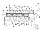
符号2aは回路基板2の「上面」を表し、符号3aは光素子シリコンチップ3の「下面」を表す。図1に示すように、光素子シリコンチップ3は、半田バンプ4を介して回路基板2の上面2aにフリップチップボンディングされており、光素子シリコンチップ3の下面3aと回路基板2の上面2aとが対向して配置されている。符号Gcは、回路基板2の上面2aと光素子シリコンチップ3の下面3aとが離間する寸法である「接合ギャップ」(「接合クリアランス」ともいう)を表す。本実施形態において、半導体装置1における接合ギャップGcの大きさは特段限定されるものではないが、例えば200μm程度に設定されている。
ところで、本実施形態に係る半導体装置1のような、いわゆる光モジュールでは、光素子シリコンチップ3の光伝送特性を担保するためにも、接合ギャップGcを設計値通りに精度良く実現する必要がある。光素子シリコンチップ3及び回路基板2は、半田バンプ4を介して接合されるため、半田バンプ4における高さ方向についての高い精度が要求される。更に、光素子シリコンチップ3等の半導体光素子は、耐熱温度が例えば160〜180℃程度といったように比較的低いものが多い。よって、光素子シリコンチップ3の実装時においては、光素子シリコンチップ3の耐熱温度を考慮して、リフロー温度をあまり高くすることができないという制約がある。ここで、従来のバンプ形成方法として、めっき法、蒸着法、印刷法等が知られている。しかしながら、めっき法は、低温での接合では接合信頼性が十分とはいえず、蒸着法や印刷法では大きな接合ギャップを形成することが難しいことから、回路基板に対する半導体光素子の接合にはいずれの方法もあまり向いていないといえる。 By the way, in the so-called optical module such as the
そこで、本実施形態に係る半導体装置1では、回路基板2及び光素子シリコンチップ3を接合する半田バンプ4を、高融点半田接合部41と低融点半田接合部42とを含んで形成することとした。高融点半田接合部41は、例えばSnAgCu系半田(錫―銀―銅系半田)等といった高融点半田(高温半田)によって形成された半田ボールである。一方、低融点半田接合部42は、例えばSnBi系半田(錫―ビスマス系半田)等といった低融点半田(低温半田)によって形成されている。低融点半田接合部42の融点(例えば、139℃程度)は、高融点半田接合部41の融点(例えば、220℃程度)よりも低くなっている。 Therefore, in the
ここで、高融点半田接合部41は、回路基板2の上面2aに形成された電極パッド(以下、「基板側パッド」という)23に接合されている。一方、低融点半田接合部42は、光素子シリコンチップ3の下面3aに形成された電極パッド(以下、「素子側パッド」という)33に接合されている。そして、半田バンプ4は、高融点半田接合部41と低融点半田接合部42とを低温の温度階層接合を行うことで一体に接合することで形成されている。具体的には、高融点半田接合部41と低融点半田接合部42とをリフローする際、高融点半田接合部41の融点よりも低温かつ低融点半田接合部42の融点よりも高温のリフロー温度でリフローすることにより、双方が一体に接合されている。更に、半田バンプ4における高融点半田接合部41と低融点半田接合部42との接合境界面には、凹凸形状を有する凹凸接合部43が形成されている。また、符号7、7Aは、モールド樹脂と第2モールド樹脂を表す。モールド樹脂7と第2モールド樹脂7Aについては後述する。 Here, the high melting point
<<半導体素子の実装方法>>
次に、光素子シリコンチップ3の実装方法について説明する。図2〜図11は、光素子シリコンチップ31の実装工程を説明する図である。<< Semiconductor Device Mounting Method >>
Next, a method for mounting the optical
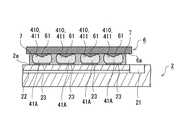
半導体装置1の製造に際して、図2に示す回路基板2を準備する。回路基板2は、例えば、エポキシ樹脂等によって形成された樹脂基板であるが、これには限定されない。回路基板2の上面2aにおける適所には複数の基板側パッド23が露出形成されている。また、回路基板2には、光素子シリコンチップ3の発光部31から出力される光を受光する受光部21や、導波路22等が形成されている。 When manufacturing the
次に、図3に示すように、SnAgCu系半田(錫―銀―銅系半田)等といった高融点半田(高温半田)によって形成された半田ボール(以下、「高融点半田ボール」という)41Aを、回路基板2の各基板側パッド23に取り付ける。高融点半田ボール41Aは、回路基板2に対する光素子シリコンチップ3の実装後において、図1に示した半田バンプ4の高融点半田接合部41を形成する。高融点半田ボール41Aの基板側パッド23への
取り付けは、以下の手順で行うことができる。まず、基板側パッド23上にフラックスを供給する。基板側パッド23上へのフラックスの供給は、印刷装置を用いたスキージングによって行ってもよい。基板側パッド23に対するフラックスの塗布が終わると、フラックス上に高融点半田ボール41Aを搭載し、リフロー炉によって加熱(リフロー)を行う。ここでのリフロー温度は、高融点半田ボール41Aの溶融温度よりも高い温度(例えば、235℃程度)としてもよい。リフローを行うことにより、高融点半田ボール41Aが溶融し、各基板側パッド23に対して高融点半田ボール41Aが一体に接合される。本実施形態において、高融点半田ボール41Aは、第1半田接合材料の一例である。Next, as shown in FIG. 3, a solder ball (hereinafter referred to as “high melting point solder ball”) 41A formed of high melting point solder (high temperature solder) such as SnAgCu solder (tin-silver-copper solder) or the like is used. Attach to each board-
次に、図4に示すような、凹部形成用の治具(以下、「凹部形成用治具」という)6を準備する。凹部形成用治具6は、回路基板2に対する光素子シリコンチップ3の実装に用いる半導体製造装置(フリップチップボンダー)に搭載されており、半導体製造装置から熱の供給を受けることで加熱される。凹部形成用治具6の下面6aには、半田ボール41の平面的な配置パターンに対応するように複数の突起61が設けられている。本実施形態においては、突起61は略円錐形状を有しているが、突起61の形状は適宜変更することができる。また、凹部形成用治具6の下面6aのうち、突起61が形成されていない部分には平坦な平坦部62が形成されている。本実施形態においては、凹部形成用治具6は、ガラス板によって形成されている。但し、凹部形成用治具6は、他の材料を用いて形成されてもよい。 Next, a recess-forming jig (hereinafter referred to as “recess-forming jig”) 6 as shown in FIG. 4 is prepared. The
次に、図5に示すように、凹部形成用治具6を、高融点半田ボール41Aの頭頂部410に押し付ける。上記のように、凹部形成用治具6の下面6aに形成された各突起61は、回路基板2に取り付けられた高融点半田ボール41Aの平面配置パターンと対応付けられて配置されている。ここでは、凹部形成用治具6の各突起61が、対応する高融点半田ボール41Aの頭頂部410に食い込むように、高融点半田ボール41Aに対して凹部形成用治具6が押し付けられる。 Next, as shown in FIG. 5, the
本実施形態では、凹部形成用治具6を、例えば150〜180℃程度に加熱しつつ高融点半田ボール41Aの頭頂部410に押し付ける。これにより、凹部形成用治具6からの伝わる熱によって高融点半田ボール41Aが軟化するため、高融点半田ボール41Aに作用する応力を低減しつつ、高融点半田ボール41Aの頭頂部410に突起61を食い込ませることができる。その結果、図5に示すように、高融点半田ボール41Aの頭頂部410には、突起61に対応する円錐形状の凹部411(凹凸形状)が形成される(凹部形成工程)。なお、本実施形態では、各高融点半田ボール41Aの頭頂部410に対して、単一の凹部411が形成されるようにしているが、複数の凹部411が一の高融点半田ボール41Aに形成されてもよい。また、凹部形成用治具6における突起61の高さは、高融点半田ボール41Aに形成する凹部411の深さに応じて適宜変更することができる。 In the present embodiment, the
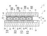
次に、高融点半田ボール41Aの頭頂部410に、凹部形成用治具6を押し付けた状態で、図6に示すように、回路基板2上に封止材料としてのモールド樹脂7を供給する。そして、少なくとも高融点半田ボール41Aの頭頂部410が露出するように高融点半田ボール41Aを封止する(封止工程)。本実施形態では、モールド樹脂7として、熱可塑性樹脂を用いるようにした。熱可塑性樹脂としては、例えば熱可塑性エポキシ樹脂を好適に使用することができる。 Next, in a state where the
封止工程においては、例えば80℃程度に加熱して軟化した状態のモールド樹脂7を、回路基板2の上面2aに流し込む。その際、高融点半田ボール41Aの頭頂部410に凹部形成用治具6が残されているため、モールド樹脂7によって高融点半田ボール41Aの頭頂部410が覆われることを抑制することができる。つまり、高融点半田ボール41Aの頭頂部410に凹部形成用治具6を押し付けた状態で封止工程を行うことにより、モー
ルド樹脂7によって凹部411が覆われることを抑制することができる。以上のように、本実施形態では、高融点半田ボール41Aの頭頂部410を残して、高融点半田ボール41Aの周囲がモールド樹脂7によって被覆される。その後、モールド樹脂7を冷却することで硬化した後、高融点半田ボール41Aから凹部形成用治具6が取り外される。In the sealing step, for example, the
上記のように、凹部形成用治具6の下面6aには、平坦部62が形成されている。従って、高融点半田ボール41Aの頭頂部410に凹部形成用治具6を取り付けた状態で封止工程を行うことにより、モールド樹脂7の上面を凹部形成用治具6の平坦部62によって平坦にすることができる(平坦化工程)。従って、図7に示すように、凹部形成用治具6を高融点半田ボール41Aから取り外した状態では、凹部形成用治具6の頭頂部410に凹部411が形成され、この凹部411の外周縁部にはモールド樹脂7の平坦化された平坦面71が連なって配置される。 As described above, the
次に、図8に示すように、所定の位置に貫通孔8aが形成されたスクリーン版8を、回路基板2の上に載置する。スクリーン版8は、図示のように、モールド樹脂7の平坦面71の上に設置される。スクリーン版8には、高融点半田ボール41Aの平面的な配置パターンに対応する位置に複数の貫通孔8aが形成されている。スクリーン版8を回路基板2上に設置する際、各貫通孔8aの位置を対応する高融点半田ボール41A(凹部411)の位置に合わせる位置合わせを行う。 Next, as shown in FIG. 8, the
次に、図9に示すように、例えばSnBi系半田(錫―ビスマス系半田)等から形成される低融点半田ペースト42Aを、例えば印刷装置を用いてスクリーン版8の上に供給する。低融点半田ペースト42Aは、回路基板2に対する光素子シリコンチップ3の実装後において、図1に示した半田バンプ4の低融点半田接合部42を形成する。印刷装置により供給された低融点半田ペースト42Aは、例えば、スキージを用いたスキージングによって、各貫通孔8aを通じて高融点半田ボール41Aの凹部411に充填される。低融点半田ペースト42Aの融点は139℃程度であって、高融点半田ボール41Aの融点(220℃程度)よりも低い。本実施形態において、低融点半田ペースト42Aは第2半田接合材料の一例である。 Next, as shown in FIG. 9, for example, a low-melting-
低融点半田ペースト42Aの供給に際して、各高融点半田ボール41A間の隙間は既にモールド樹脂7によって被覆されている。従って、スキージを用いたスキージングによって、スクリーン版8が面方向に相対ずれを起こす方向に力が作用しても、高融点半田ボール41Aや、高融点半田ボール41Aと基板側パッド23との接合部に作用する応力を低減することができる。これにより、高融点半田ボール41Aや、高融点半田ボール41Aと基板側パッド23との接合箇所にひび割れ等の損傷が生じることを抑制することができる。 When supplying the low melting
また、スクリーン版8をモールド樹脂7の平坦面71上に設置することができるため、スキージの調整精度を比較的ラフに行っても、低融点半田ペースト42Aを高精度に印刷することができ、作業効率の向上を図ることができる。更に、高融点半田ボール41Aの周囲をモールド樹脂7で被覆することにより、スクリーン版8の貫通孔8aに流入した低融点半田ペースト42Aが、貫通孔8aと高融点半田ボール41Aとの隙間から漏れ出すことが抑制される。これにより、高融点半田ボール41Aの上に、適正な量の低融点半田ペースト42Aを精度良く供給することができる。また、高融点半田ボール41Aからの低融点半田ペースト42Aの滑り落ちを抑制できるため、隣接する基板側パッド23同士のショートを抑制することができる。 Further, since the
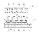
次に、回路基板2からスクリーン版8を取り外し、図10に示すように、光素子シリコンチップ3の下面3aが回路基板2の上面2aと向き合うように光素子シリコンチップ3
を配置する。光素子シリコンチップ3の下面3aにおける適所には複数の素子側パッド33が露出形成されている。また、光素子シリコンチップ3には、発光部31や導波路32が形成されている。光素子シリコンチップ3は、素子側パッド33と基板側パッド23との平面位置が合致し、かつ、回路基板2と光素子シリコンチップ3との間に所定の接合ギャップGcが設けられるように、回路基板2との相対位置が調整される。Next, the
Place. A plurality of element-
次いで、リフロー炉によって、回路基板2及び光素子シリコンチップ3の加熱処理(リフロー)を行う(リフロー工程)。ここで、リフローを行う際のリフロー温度(加熱温度)は、高融点半田ボール41Aの融点より低く、かつ、低融点半田ペースト42Aの融点より高い温度に設定されている。例えば、リフロー温度は160℃程度に設定されている。リフローに際して、リフロー温度が高融点半田ボール41Aの融点より低いため、高融点半田ボール41Aは形状変化を伴わず、元の形状を維持する。一方、低融点半田ペースト42Aの融点よりリフロー温度が高いため、低融点半田ペースト42Aは溶融することになる。 Next, heat treatment (reflow) of the
本実施形態において、高融点半田ボール41Aの寸法を、接合ギャップGcから基板側パッド23及び素子側パッド33の厚みを差し引いた寸法よりも若干小さめに設定している。そして、リフロー時に形状変化しない高融点半田ボール41Aを、接合ギャップGcを確保するためのスペーサ(空間確保部材)として利用し、素子側パッド33と高融点半田ボール41Aとの隙間を低融点半田ペースト42Aによって接続することとした。リフローによって溶融した低融点半田ペースト42Aは、高融点半田ボール41Aの半田合金内に拡散し、低融点半田ペースト42A及び高融点半田ボール41Aは一体に接合される。その後、低融点半田ペースト42A及び高融点半田ボール41Aが冷却されることで、図1に示した半田バンプ4が完成する。その際、上述の低融点半田ペースト42Aが半田バンプ4の低融点半田接合部42を形成し、高融点半田ボール41Aが半田バンプ4の高融点半田接合部41を形成することになる。 In the present embodiment, the dimension of the high melting
その後、図11に示すように、モールド樹脂7と光素子シリコンチップ3との隙間に第2モールド樹脂7Aを充填する。第2モールド樹脂7Aとしては、低融点半田42の融点よりも低温で軟化する熱硬化性樹脂を好適に用いることができる。以上の工程によって、回路基板2に対する光素子シリコンチップ3の実装工程が完了し、半導体装置1が完成する。 Thereafter, as shown in FIG. 11, the
以上のように、本実施形態に係る光素子シリコンチップ3の実装方法では、高融点半田ボール41A(高融点半田接合部41)の融点よりも低温による温度階層接合を行う。これによれば、リフロー時においても形状を維持する高融点半田ボール41Aをスペーサとして利用できるため、容易に大きな接合ギャップGcを確保することができる。また、光素子シリコンチップ3における素子側パッド33と高融点半田ボール41Aとの隙間には、リフロー時に溶融する低融点半田ペースト42Aが充填される。このため、各高融点半田ボール41Aの高さが多少ばらついていたり、光素子シリコンチップ3が多少傾いていたとしても、これらの高さ方向のばらつき(誤差)を、低融点半田ペースト42Aによって容易に吸収することができる。その結果、回路基板2及び光素子シリコンチップ3間の接合ギャップGcの設計寸法が大きくても、接合ギャップGcを設計寸法通りに精度良く形成することができる。つまり、本実施形態に係る実装方法によれば、接合ギャップGcの寸法精度を高めることができる。 As described above, in the method for mounting the optical
更に、本実施形態に係る光素子シリコンチップ3の実装工程においては、高融点半田ボール41Aの頭頂部410に凹部411を設けるようにした(図7等を参照)。これによれば、半田バンプ4の高融点半田接合部41(高融点半田ボール41A)と低融点半田接合部42(低融点半田ペースト42A)とが接合される境界面に、凹凸形状を有する凹凸
接合部43を形成することができる。このように、高融点半田接合部41及び低融点半田接合部42の接合境界面に凹凸接合部43を形成することで、高融点半田接合部41及び低融点半田接合部42相互の機械的噛み合い作用によって、外力に抵抗する機械的強度を大きくすることができる。Furthermore, in the mounting process of the optical
また、高融点半田接合部41及び低融点半田接合部42の接合境界面を凹凸形状とすることにより、高融点半田接合部41と低融点半田接合部42との接触面積を増やすことができる。そのため、リフロー時において、低融点半田ペースト42Aが凝集することを抑止し、低融点半田ペースト42Aの高融点半田ボール41Aへの拡散を促進させることができ、双方の一体化を促進させることができる。その結果、異種半田合金間における界面剥離が起こりにくくなり、相互の接合強度を大きくすることができる。 In addition, the contact area between the high melting point solder
以上のように、本実施形態に係る光素子シリコンチップ3の実装方法によれば、光素子シリコンチップ3と回路基板2との間の接合ギャップ(接合クリアランス)Gcを適正な値に精度良く制御することできる。しかも、光素子シリコンチップ3の実装時に、リフロー温度を比較的低く設定しても、高い接合信頼性を確保することができる。 As described above, according to the mounting method of the optical
なお、上述した光素子シリコンチップ3の実装方法において、モールド樹脂7による封止工程は、高融点半田ボール41Aの頭頂部410に凹部411を形成する前に行ってもよい。また、場合によってはモールド樹脂7による封止工程を省略することも可能である。封止工程を省略する場合においても、高融点半田ボール41Aの頭頂部410に凹部411を形成しておくことで、印刷装置から供給される低融点半田ペースト42Aを凹部411によって受け止めることができる。これにより、低融点半田ペースト42Aが高融点半田ボール41Aから滑り落ちにくくすることができる。その結果、高融点半田ボール41Aに対して適正な量の低融点半田ペースト42Aを供給することができ、半田バンプ4を介した光素子シリコンチップ3と回路基板2との接合信頼性を高めることが可能となる。 In the mounting method of the optical
また、上述した光素子シリコンチップ3の実装方法においては、モールド樹脂7の上面を平坦化する平坦化工程を、凹部形成用治具6の下面6aを利用して行うようにした。これによれば、高融点半田ボール41Aの頭頂部410に凹部411を形成する凹部形成工程と平坦化工程とを同時に行うことができる。その結果、光素子シリコンチップ3の実装に要する工数を減らすことができ、半導体装置1の製造効率を高めることができる。但し、モールド樹脂7の上面を平坦化する平坦化工程は、低融点半田42のペーストを凹部411に供給する前に行われればよく、凹部形成工程の後に行うようにしてもよい。 In the mounting method of the optical
<<半導体素子の実装方法の変形例>>
次に、光素子シリコンチップ3の実装方法の変形例について説明する。図12〜図18は、本変形例に係る光素子シリコンチップ3の実装工程を説明する図である。なお、以下では、図2〜図11を参照して説明した実装方法との相違点を中心に説明する。また、上述まで実施形態と共通する構成については同一の参照符号を付すことにより、その詳しい説明を省略する。<< Variation of mounting method of semiconductor element >>
Next, a modified example of the mounting method of the optical
本変形例に係る実装方法においても、回路基板2の各基板側パッド23に高融点半田ボール41Aを取り付けるまでは、既述の実施形態と共通する。高融点半田ボール41Aについては、既述の通りである。次に、図12に示すように、高融点半田ボール41Aが取り付けられた状態の回路基板2の上面2aに、封止材料としてのモールド樹脂7を供給する。モールド樹脂7は、上記の通り熱可塑性樹脂によって形成されている。本変形例においては、高融点半田ボール41Aの頭頂部410が少なくとも露出するように、軟化した状態のモールド樹脂7を供給し、モールド樹脂7によって高融点半田ボール41Aを封止
する(封止工程)。なお、封止工程において供給されたモールド樹脂7の上面は平坦になっていなくてもよい。The mounting method according to this modification is also common to the above-described embodiment until the high melting
次に、図13に示す突起付きスクリーン版8Aを準備する。突起付きスクリーン版8Aは、上述したスクリーン版8と同様、高融点半田ボール41Aの配置パターンと対応する位置に複数の貫通孔8aが形成されている。また、突起付きスクリーン版8Aの下面80には、複数の突起81が形成されている。突起81は、突起付きスクリーン版8Aにおける下面80のうち各貫通孔8aの周縁近傍に2つずつ設けられており、下面80から下方に向けて突設されている。但し、各貫通孔8aに対応する突起81の数は、適宜変更することができる。また、突起付きスクリーン版8Aの下面のうち、突起81が形成されていない部分には平坦な平坦部82が形成されている。 Next, a
次に、図14に示すように、各貫通孔8aを対応する高融点半田ボール41Aの位置に合わせる位置合わせを行いつつ、突起付きスクリーン版8Aを回路基板2の上に載置する。ここで、突起付きスクリーン版8Aを回路基板2の上に載置する際、突起付きスクリーン版8Aの下面80に設けられた突起81を、高融点半田ボール41Aの頭頂部410に押し付け、食い込ませる。これにより、各高融点半田ボール41Aの頭頂部410に、凹部411Aが形成される。本変形例では、突起付きスクリーン版8Aにおける各貫通孔8aの周縁に2つの突起81を設けているため、各高融点半田ボール41Aの頭頂部410には2つの凹部411Aが形成されることになる(凹部形成工程)。なお、本変形例において、凹部形成工程は、モールド樹脂7が硬化する前に行われる。突起付きスクリーン版8Aの平坦部82が軟化した状態のモールド樹脂7の上面に押し付けられることで、モールド樹脂7の上面に平坦面71を形成することができる。つまり、モールド樹脂7における上面の平坦化を行うことができる。 Next, as shown in FIG. 14, the
ここで、高融点半田ボール41Aは、その周囲に充填されたモールド樹脂7によって封止されている。そのため、突起付きスクリーン版8Aの突起81を高融点半田ボール41Aの頭頂部410に押し付けて凹部411Aを形成する際、高融点半田ボール41Aと基板側パッド23との接合部に大きな応力が作用することを抑制できる。以上のように、本変形例では、封止工程を凹部形成工程の前に行う。 Here, the high melting
次に、図15に示すように、低融点半田ペースト42Aを、例えば印刷装置を用いて突起付きスクリーン版8A上に供給する。低融点半田ペースト42Aについては既述の通りである。印刷装置により供給された低融点半田ペースト42Aは、スキージを用いたスキージングによって、各貫通孔8aを通じて高融点半田ボール41Aの頭頂部410に供給される。 Next, as shown in FIG. 15, the low-melting-
本変形例においても、低融点半田ペースト42Aを高融点半田ボール41Aの頭頂部410に供給する際に、高融点半田ボール41Aの周囲はモールド樹脂7によって被覆(封止)されている。従って、低融点半田ペースト42Aを高融点半田ボール41Aの頭頂部410から滑り落ちることを抑制し、適正な量の低融点半田ペースト42Aを高融点半田ボール41A上に精度良く転写することができる。更に、モールド樹脂7の上面には、平坦な平坦面71が形成されているため、低融点半田ペースト42Aを精度良く印刷することができる。また、低融点半田ペースト42Aの供給時に、高融点半田ボール41Aと基板側パッド23との接合部に作用する応力を低減することができるので、上記接合部の破損を抑制することができる。 Also in this modification, when the low melting
次に、回路基板2から突起付きスクリーン版8Aを取り外す。その結果、図16に示すように、突起付きスクリーン版8Aの貫通孔8aに充填されていた低融点半田ペースト42Aが、高融点半田ボール41Aの頭頂部410に形成された凹部411Aに流れ込み、
充填される。次に、図17に示すように、光素子シリコンチップ3の下面3aが回路基板2の上面2aと向き合うように光素子シリコンチップ3を配置する。光素子シリコンチップ3は、素子側パッド33と基板側パッド23との平面位置が合致し、かつ、回路基板2と光素子シリコンチップ3との間に所定の接合ギャップGcが設けられるように、回路基板2との相対位置が調整される。Next, the screen plate with
Filled. Next, as shown in FIG. 17, the optical
次いで、リフロー炉によって、回路基板2及び光素子シリコンチップ3の加熱処理(リフロー)を行う(リフロー工程)。リフロー温度は、上記実施形態と同様、高融点半田ボール41Aの融点より低く、かつ、低融点半田ペースト42Aの融点より高い温度に設定されている。従って、上記実施形態と同様に、リフロー時においては、低融点半田ペースト42Aが溶融する一方、高融点半田ボール41Aはリフロー前の形状を維持することになる。本変形例においても、高融点半田ボール41Aの寸法を、接合ギャップGcから基板側パッド23及び素子側パッド33の厚みを差し引いた寸法よりも若干小さめに設定している。そして、リフロー時に形状変化しない高融点半田ボール41Aを、接合ギャップGcを確保するためのスペーサとして利用し、素子側パッド33と高融点半田ボール41Aとの隙間を低融点半田ペースト42Aによって接続する。その後、低融点半田ペースト42A及び高融点半田ボール41Aが冷却されることで、上記実施形態と同様に半田バンプ4が形成される。その際、低融点半田ペースト42Aが半田バンプ4の低融点半田接合部42を形成し、高融点半田ボール41Aが半田バンプ4の高融点半田接合部41を形成することになる。 Next, heat treatment (reflow) of the
その後、図18に示すように、モールド樹脂7と光素子シリコンチップ3との隙間に第2モールド樹脂7Aを充填する。第2モールド樹脂7Aとしては、低融点半田42の融点よりも低温で軟化する熱硬化性樹脂を好適に用いることができる。以上の工程によって、回路基板2に対する光素子シリコンチップ3の実装工程が完了し、半導体装置1が完成する。 Thereafter, as shown in FIG. 18, the
本変形例においても、高融点半田ボール41Aの頭頂部410に凹部411Aを設けるようにした。これによれば、半田バンプ4の高融点半田接合部41(高融点半田ボール41A)と低融点半田接合部42(低融点半田ペースト42A)とが接合される境界面に凹凸形状を有する凹凸接合部43が形成される。その結果、高融点半田接合部41及び低融点半田接合部42相互の機械的噛み合い作用によって、半田バンプ4の外力に抵抗する機械的強度を大きくすることができる。そして、凹凸形状を有する凹凸接合部43によって、高融点半田接合部41と低融点半田接合部42との接触面積を増やすことができる。このため、異種半田合金間における界面剥離が起こりにくくなり、高融点半田接合部41及び低融点半田接合部42間における接合強度を大きくすることができる。これにより、半田バンプ4を介した回路基板2及び光素子シリコンチップ3の優れた接合(接続)信頼性を実現することができる。そして、リフロー温度を高融点半田ボール41A(高融点半田接合部41)の融点よりも低温とする温度階層接合を行うことで、より大きな接合ギャップGcが容易に得られるようになり、しかも、接合ギャップGcの寸法精度を従来よりも高めることができる。つまり、回路基板2と光素子シリコンチップ3との間の接合ギャップGcの設計寸法が大きくても、形成する接合ギャップGcの寸法精度を好適に高めることができる。 Also in this modification, the
更に、本変形例に係る実装方法においては、突起81及び平坦部82を有する突起付きスクリーン版8Aを用いて、低融点半田ペースト42Aを高融点半田ボール41Aの頭頂部410に転写するようにした。これによれば、高融点半田ボール41Aの頭頂部410に対する低融点半田ペースト42Aの転写と、高融点半田ボール41Aの頭頂部410への凹部411Aの形成と、モールド樹脂7の上面の平坦化を、一括して(同一工程で)行うことができる。その結果、光素子シリコンチップ3の実装に要する工数を減らすことが
でき、半導体装置1の製造効率を高めることができる。Furthermore, in the mounting method according to this modification, the low melting
また、本変形例においては、高融点半田ボール41Aの周囲をモールド樹脂7によって封止した状態で、高融点半田ボール41Aの頭頂部410に凹部411Aを形成する点で、上記実施形態と相違する。これによれば、突起付きスクリーン版8Aの突起81を高融点半田ボール41Aの頭頂部410に押し付ける際に、高融点半田ボール41Aと基板側パッド23との接合部に作用する応力を好適に低減することができる。その結果、高融点半田ボール41Aと基板側パッド23との接合部を、より一層破損しにくくすることが可能となる。 Further, the present modification is different from the above embodiment in that the
以上、実施形態に沿って本件に係る半導体装置及び半導体素子の実装方法について説明したが、本件はこれらに制限されるものではない。そして、上記実施形態について、種々の変更、改良、組み合わせ等が可能なことは当業者にとって自明である。例えば、上記実施形態及び変形例において、回路基板2に対して実装する半導体素子をVCSEL等の発光素子とする場合を例示的に説明したが、フォトダイオード等の受光素子であってもよい。また、VCSELやフォトダイオード等の光素子に限られず、種々の半導体素子を実装する際に本件に係る実装方法を好適に適用することができる。 As described above, the semiconductor device and the semiconductor element mounting method according to the present embodiment have been described according to the embodiment, but the present embodiment is not limited thereto. It is obvious to those skilled in the art that various changes, improvements, combinations, and the like are possible for the above-described embodiment. For example, in the above embodiment and the modification, the case where the semiconductor element mounted on the
1・・・半導体装置
2・・・回路基板
3・・・光素子シリコンチップ
4・・・半田バンプ
6・・・凹部形成用治具
7・・・モールド樹脂
23・・・基板側パッド
33・・・素子側パッド
41・・・高融点半田接合部
41A・・・高融点半田ボール
42・・・低融点半田接合部
42A・・・低融点半田ペースト
43・・・凹凸接合部
410・・・頭頂部
411・・・凹部
Gc・・・接合ギャップDESCRIPTION OF
Claims (7)
Translated fromJapanese前記基板に形成された基板側パッド上に第1半田接合材料を取り付ける工程と、
前記第1半田接合材料上に該第1半田接合材料よりも融点が低い第2半田接合材料を供給する工程と、
前記半導体素子に形成された素子側パッドが対応する前記基板側パッドに対向し、かつ、前記基板との間に所定の接合ギャップが設けられるように前記半導体素子を配置する工程と、
前記第1半田接合材料の融点よりも低温かつ前記第2半田接合材料の融点よりも高温のリフロー温度でリフローを行い、該第1半田接合材料及び第2半田接合材料を接合するリフロー工程と、
を有する、
半導体素子の実装方法。A mounting method for mounting a semiconductor element on a substrate,
Attaching a first solder bonding material on a substrate-side pad formed on the substrate;
Supplying a second solder bonding material having a melting point lower than that of the first solder bonding material onto the first solder bonding material;
Disposing the semiconductor element such that an element-side pad formed on the semiconductor element faces the corresponding substrate-side pad and a predetermined bonding gap is provided between the substrate and the substrate;
A reflow step of performing reflow at a reflow temperature lower than the melting point of the first solder bonding material and higher than the melting point of the second solder bonding material, and bonding the first solder bonding material and the second solder bonding material;
Having
A method for mounting a semiconductor element.
前記第2半田接合材料を供給する工程においては、前記凹部に前記第2半田接合材料が充填されるように該第2半田接合材料を供給する、
請求項1に記載の半導体素子の実装方法。A recess forming step of forming a recess in the top of the first solder bonding material;
In the step of supplying the second solder bonding material, the second solder bonding material is supplied so that the second solder bonding material is filled in the recess.
The method for mounting a semiconductor device according to claim 1.
請求項2に記載の半導体素子の実装方法。Before supplying the second solder bonding material, a sealing material is supplied onto the substrate, and the first solder bonding material is sealed so that at least the top of the first solder bonding material is exposed. Further comprising a step,
A method for mounting a semiconductor element according to claim 2.
請求項3に記載の半導体素子の実装方法。A flattening step of flattening an upper surface of the sealing material before supplying the second solder bonding material;
A method for mounting a semiconductor device according to claim 3.
請求項3又は4に記載の半導体素子の実装方法。Performing the sealing step before the recess forming step;
The method for mounting a semiconductor element according to claim 3 or 4.
前記封止工程において、前記頭頂部に前記治具を押し付けた状態で前記第1半田接合材料を封止する、
請求項3から5の何れか一項に記載の半導体素子の実装方法。In the recess forming step, the recess is formed by pressing a predetermined jig against the top of the first solder joint material,
In the sealing step, the first solder bonding material is sealed in a state in which the jig is pressed against the crown.
The method for mounting a semiconductor element according to claim 3.
請求項2から6の何れか一項に記載の半導体素子の実装方法。In the recess forming step, the recess is formed while heating the top of the first solder joint material.
The method for mounting a semiconductor element according to claim 2.
Priority Applications (2)
| Application Number | Priority Date | Filing Date | Title |
|---|---|---|---|
| JP2013058764AJP6197319B2 (en) | 2013-03-21 | 2013-03-21 | Mounting method of semiconductor element |
| US14/073,998US9615464B2 (en) | 2013-03-21 | 2013-11-07 | Method of mounting semiconductor element, and semiconductor device |
Applications Claiming Priority (1)
| Application Number | Priority Date | Filing Date | Title |
|---|---|---|---|
| JP2013058764AJP6197319B2 (en) | 2013-03-21 | 2013-03-21 | Mounting method of semiconductor element |
Publications (2)
| Publication Number | Publication Date |
|---|---|
| JP2014183301A JP2014183301A (en) | 2014-09-29 |
| JP6197319B2true JP6197319B2 (en) | 2017-09-20 |
Family
ID=51568998
Family Applications (1)
| Application Number | Title | Priority Date | Filing Date |
|---|---|---|---|
| JP2013058764AExpired - Fee RelatedJP6197319B2 (en) | 2013-03-21 | 2013-03-21 | Mounting method of semiconductor element |
Country Status (2)
| Country | Link |
|---|---|
| US (1) | US9615464B2 (en) |
| JP (1) | JP6197319B2 (en) |
Families Citing this family (11)
| Publication number | Priority date | Publication date | Assignee | Title |
|---|---|---|---|---|
| US9110234B2 (en)* | 2010-12-28 | 2015-08-18 | Kyocera Corporation | Optical module and optical wiring board |
| WO2014061085A1 (en)* | 2012-10-15 | 2014-04-24 | 千住金属工業株式会社 | Soldering method for low-temperature solder paste |
| JP6307131B2 (en)* | 2015-09-08 | 2018-04-04 | エルジー エレクトロニクス インコーポレイティド | Solar cell module and manufacturing method thereof |
| CN109661726A (en)* | 2017-01-20 | 2019-04-19 | 联想(新加坡)私人有限公司 | Method of solder bonding and soldered fitting |
| US10586782B2 (en) | 2017-07-01 | 2020-03-10 | International Business Machines Corporation | Lead-free solder joining of electronic structures |
| CN108346952B (en)* | 2018-01-25 | 2020-11-24 | 番禺得意精密电子工业有限公司 | Electric connector holder |
| CN110718524B (en)* | 2019-08-30 | 2024-03-15 | 华为技术有限公司 | Electronic component and electronic device |
| US11557878B2 (en)* | 2019-10-22 | 2023-01-17 | University Of Maryland, College Park | High power, narrow linewidth semiconductor laser system and method of fabrication |
| JP6767665B1 (en)* | 2020-06-10 | 2020-10-14 | 千住金属工業株式会社 | How to form a bump electrode substrate |
| DE102021103360A1 (en)* | 2021-02-05 | 2022-08-11 | Few Fahrzeugelektrik Werk Gmbh & Co. Kg | Method of making a pre-tinning assembly and such pre-tinning assembly |
| JPWO2022172927A1 (en)* | 2021-02-10 | 2022-08-18 |
Family Cites Families (42)
| Publication number | Priority date | Publication date | Assignee | Title |
|---|---|---|---|---|
| DE3824865A1 (en)* | 1988-07-21 | 1990-01-25 | Productech Gmbh | MANUFACTURE OF SOLAR AREAS |
| JP3049800B2 (en) | 1991-02-28 | 2000-06-05 | 日本電気株式会社 | Method for forming bump electrode of semiconductor light receiving element |
| US5203075A (en)* | 1991-08-12 | 1993-04-20 | Inernational Business Machines | Method of bonding flexible circuit to cicuitized substrate to provide electrical connection therebetween using different solders |
| US5545589A (en)* | 1993-01-28 | 1996-08-13 | Matsushita Electric Industrial Co., Ltd. | Method of forming a bump having a rugged side, a semiconductor device having the bump, and a method of mounting a semiconductor unit and a semiconductor device |
| US5477086A (en)* | 1993-04-30 | 1995-12-19 | Lsi Logic Corporation | Shaped, self-aligning micro-bump structures |
| US5470787A (en)* | 1994-05-02 | 1995-11-28 | Motorola, Inc. | Semiconductor device solder bump having intrinsic potential for forming an extended eutectic region and method for making and using the same |
| JPH0829638A (en)* | 1994-05-12 | 1996-02-02 | Fujitsu Ltd | Optical waveguide / optical fiber connection structure, optical waveguide / optical fiber connection method, optical waveguide substrate used for optical waveguide / optical fiber connection, method of manufacturing the same, and optical fiber with optical fiber substrate used for optical waveguide / optical fiber connection fiber |
| JP3348528B2 (en)* | 1994-07-20 | 2002-11-20 | 富士通株式会社 | Method for manufacturing semiconductor device, method for manufacturing semiconductor device and electronic circuit device, and electronic circuit device |
| DE19511898C2 (en)* | 1995-03-31 | 1999-09-23 | Fraunhofer Ges Forschung | Method for connecting contact surfaces of an electronic component and a substrate |
| US5889326A (en)* | 1996-02-27 | 1999-03-30 | Nec Corporation | Structure for bonding semiconductor device to substrate |
| JPH1013007A (en)* | 1996-03-29 | 1998-01-16 | Ngk Spark Plug Co Ltd | Wiring board with solder bump, its manufacturing method, and flattening tool |
| JPH09275269A (en)* | 1996-04-01 | 1997-10-21 | Omron Corp | Method of mounting electronic elements on circuit board, electronic elements and circuit board used therefor |
| JP3145331B2 (en)* | 1996-04-26 | 2001-03-12 | 日本特殊陶業株式会社 | Relay board, method of manufacturing the same, structure including substrate, relay board, and mounting board, connection body of substrate and relay board, and method of manufacturing connection body of relay board and mounting board |
| JP3180041B2 (en)* | 1996-10-09 | 2001-06-25 | 住友金属工業株式会社 | Connection terminal and method of forming the same |
| US5872400A (en)* | 1997-06-25 | 1999-02-16 | International Business Machines Corporation | High melting point solder ball coated with a low melting point solder |
| US5984164A (en)* | 1997-10-31 | 1999-11-16 | Micron Technology, Inc. | Method of using an electrically conductive elevation shaping tool |
| DE19750073A1 (en)* | 1997-11-12 | 1999-05-20 | Bosch Gmbh Robert | Circuit board |
| JP3344956B2 (en)* | 1998-01-08 | 2002-11-18 | 日本特殊陶業株式会社 | Manufacturing method of multilayer ceramic substrate |
| US6046910A (en)* | 1998-03-18 | 2000-04-04 | Motorola, Inc. | Microelectronic assembly having slidable contacts and method for manufacturing the assembly |
| JP3975569B2 (en)* | 1998-09-01 | 2007-09-12 | ソニー株式会社 | Mounting substrate and manufacturing method thereof |
| US6225206B1 (en)* | 1999-05-10 | 2001-05-01 | International Business Machines Corporation | Flip chip C4 extension structure and process |
| US6267650B1 (en)* | 1999-08-09 | 2001-07-31 | Micron Technology, Inc. | Apparatus and methods for substantial planarization of solder bumps |
| JP2001085470A (en)* | 1999-09-16 | 2001-03-30 | Fujitsu Ltd | Semiconductor device and manufacturing method thereof |
| US6683387B1 (en)* | 2000-06-15 | 2004-01-27 | Advanced Micro Devices, Inc. | Flip chip carrier package with adapted landing pads |
| JP4609617B2 (en)* | 2000-08-01 | 2011-01-12 | 日本電気株式会社 | Semiconductor device mounting method and mounting structure |
| US7414319B2 (en)* | 2000-10-13 | 2008-08-19 | Bridge Semiconductor Corporation | Semiconductor chip assembly with metal containment wall and solder terminal |
| JP2002190497A (en)* | 2000-12-21 | 2002-07-05 | Sony Corp | Sealing resin for flip-chip mounting |
| JP4131623B2 (en) | 2001-09-12 | 2008-08-13 | 三洋電機株式会社 | Electrode structure and manufacturing method thereof |
| US6583517B1 (en)* | 2002-04-09 | 2003-06-24 | International Business Machines Corporation | Method and structure for joining two substrates with a low melt solder joint |
| JP2004012803A (en)* | 2002-06-06 | 2004-01-15 | Fujitsu Ltd | Printed circuit board unit for optical transmission and mounting method |
| JP2004103928A (en)* | 2002-09-11 | 2004-04-02 | Fujitsu Ltd | Method for forming substrate and solder ball and mounting structure thereof |
| JP3905100B2 (en)* | 2004-08-13 | 2007-04-18 | 株式会社東芝 | Semiconductor device and manufacturing method thereof |
| US7611040B2 (en)* | 2005-05-24 | 2009-11-03 | Panasonic Corporation | Method for forming solder bump and method for mounting semiconductor device using a solder powder resin composition |
| JP4251458B2 (en)* | 2005-12-21 | 2009-04-08 | Tdk株式会社 | Chip component mounting method and circuit board |
| JP2008071792A (en)* | 2006-09-12 | 2008-03-27 | Toshiba Corp | Manufacturing method of semiconductor device |
| JP5066935B2 (en)* | 2007-02-22 | 2012-11-07 | 富士通株式会社 | Method for manufacturing electronic component and electronic device |
| US8390117B2 (en)* | 2007-12-11 | 2013-03-05 | Panasonic Corporation | Semiconductor device and method of manufacturing the same |
| JP5533665B2 (en)* | 2008-11-28 | 2014-06-25 | 富士通株式会社 | Electronic device manufacturing method, electronic component mounting substrate, and manufacturing method thereof |
| JP2013093405A (en)* | 2011-10-25 | 2013-05-16 | Ngk Spark Plug Co Ltd | Wiring board and manufacturing method of the same |
| JP5800674B2 (en)* | 2011-10-25 | 2015-10-28 | 日本特殊陶業株式会社 | Wiring board and manufacturing method thereof |
| US8828860B2 (en)* | 2012-08-30 | 2014-09-09 | International Business Machines Corporation | Double solder bumps on substrates for low temperature flip chip bonding |
| US8920934B2 (en)* | 2013-03-29 | 2014-12-30 | Intel Corporation | Hybrid solder and filled paste in microelectronic packaging |
- 2013
- 2013-03-21JPJP2013058764Apatent/JP6197319B2/ennot_activeExpired - Fee Related
- 2013-11-07USUS14/073,998patent/US9615464B2/ennot_activeExpired - Fee Related
Also Published As
| Publication number | Publication date |
|---|---|
| JP2014183301A (en) | 2014-09-29 |
| US20140285989A1 (en) | 2014-09-25 |
| US9615464B2 (en) | 2017-04-04 |
Similar Documents
| Publication | Publication Date | Title |
|---|---|---|
| JP6197319B2 (en) | Mounting method of semiconductor element | |
| JP4928945B2 (en) | Bump-on-lead flip chip interconnect | |
| CN101996902B (en) | The manufacture method of semiconductor device | |
| CN101252093B (en) | Manufacturing method of electronic component and electronic device, electronic component and electronic device | |
| TWI397978B (en) | Structure of chip and process thereof and structure of flip chip package and process thereof | |
| JP4907500B2 (en) | Method for forming conductive bump | |
| JP5160390B2 (en) | Wiring board with lead pins and method for manufacturing the same | |
| JP2008109059A (en) | Method of packaging electronic component on substrate and method of forming solder face | |
| JP5422830B2 (en) | Wiring board with lead pins and method for manufacturing the same | |
| CN107078118A (en) | Interposer to Package Substrate Coupling | |
| JP2007243106A (en) | Semiconductor package structure | |
| JP2010123676A (en) | Manufacturing method of semiconductor device and semiconductor device | |
| JP2007258448A (en) | Semiconductor device | |
| JP5889160B2 (en) | Manufacturing method of electronic equipment | |
| JP5212392B2 (en) | Semiconductor device | |
| JP2006351935A (en) | Semiconductor chip mounting substrate and semiconductor device using it | |
| JP2004281634A (en) | Method for manufacturing stacked package semiconductor device | |
| JP2007208056A (en) | Method of manufacturing semiconductor device | |
| JP4752717B2 (en) | Module manufacturing method | |
| JP6877271B2 (en) | Manufacturing method of optical module | |
| JP4200090B2 (en) | Manufacturing method of semiconductor device | |
| JP2008192833A (en) | Manufacturing method of semiconductor device | |
| JP2009110991A (en) | Semiconductor device and manufacturing method thereof | |
| CN100542380C (en) | Electronic component mounting method and circuit board and circuit board unit used therefor | |
| JP5576053B2 (en) | Semiconductor device manufacturing method and circuit board sheet |
Legal Events
| Date | Code | Title | Description |
|---|---|---|---|
| A621 | Written request for application examination | Free format text:JAPANESE INTERMEDIATE CODE: A621 Effective date:20151106 | |
| A977 | Report on retrieval | Free format text:JAPANESE INTERMEDIATE CODE: A971007 Effective date:20160907 | |
| A131 | Notification of reasons for refusal | Free format text:JAPANESE INTERMEDIATE CODE: A131 Effective date:20161004 | |
| A521 | Request for written amendment filed | Free format text:JAPANESE INTERMEDIATE CODE: A523 Effective date:20161130 | |
| A131 | Notification of reasons for refusal | Free format text:JAPANESE INTERMEDIATE CODE: A131 Effective date:20170509 | |
| A521 | Request for written amendment filed | Free format text:JAPANESE INTERMEDIATE CODE: A523 Effective date:20170630 | |
| TRDD | Decision of grant or rejection written | ||
| A01 | Written decision to grant a patent or to grant a registration (utility model) | Free format text:JAPANESE INTERMEDIATE CODE: A01 Effective date:20170725 | |
| A61 | First payment of annual fees (during grant procedure) | Free format text:JAPANESE INTERMEDIATE CODE: A61 Effective date:20170807 | |
| R150 | Certificate of patent or registration of utility model | Ref document number:6197319 Country of ref document:JP Free format text:JAPANESE INTERMEDIATE CODE: R150 | |
| LAPS | Cancellation because of no payment of annual fees |