JP6195399B2 - Bendable and stretchable electronic device and manufacturing method thereof - Google Patents
Bendable and stretchable electronic device and manufacturing method thereofDownload PDFInfo
- Publication number
- JP6195399B2 JP6195399B2JP2016533302AJP2016533302AJP6195399B2JP 6195399 B2JP6195399 B2JP 6195399B2JP 2016533302 AJP2016533302 AJP 2016533302AJP 2016533302 AJP2016533302 AJP 2016533302AJP 6195399 B2JP6195399 B2JP 6195399B2
- Authority
- JP
- Japan
- Prior art keywords
- trace
- traces
- bond pads
- die
- sealing material
- Prior art date
- Legal status (The legal status is an assumption and is not a legal conclusion. Google has not performed a legal analysis and makes no representation as to the accuracy of the status listed.)
- Active
Links
Images


Classifications
- B—PERFORMING OPERATIONS; TRANSPORTING
- B32—LAYERED PRODUCTS
- B32B—LAYERED PRODUCTS, i.e. PRODUCTS BUILT-UP OF STRATA OF FLAT OR NON-FLAT, e.g. CELLULAR OR HONEYCOMB, FORM
- B32B27/00—Layered products comprising a layer of synthetic resin
- B32B27/06—Layered products comprising a layer of synthetic resin as the main or only constituent of a layer, which is next to another layer of the same or of a different material
- B32B27/08—Layered products comprising a layer of synthetic resin as the main or only constituent of a layer, which is next to another layer of the same or of a different material of synthetic resin
- H—ELECTRICITY
- H01—ELECTRIC ELEMENTS
- H01L—SEMICONDUCTOR DEVICES NOT COVERED BY CLASS H10
- H01L23/00—Details of semiconductor or other solid state devices
- H01L23/48—Arrangements for conducting electric current to or from the solid state body in operation, e.g. leads, terminal arrangements ; Selection of materials therefor
- H01L23/488—Arrangements for conducting electric current to or from the solid state body in operation, e.g. leads, terminal arrangements ; Selection of materials therefor consisting of soldered or bonded constructions
- H01L23/498—Leads, i.e. metallisations or lead-frames on insulating substrates, e.g. chip carriers
- H01L23/4985—Flexible insulating substrates
- B—PERFORMING OPERATIONS; TRANSPORTING
- B23—MACHINE TOOLS; METAL-WORKING NOT OTHERWISE PROVIDED FOR
- B23B—TURNING; BORING
- B23B5/00—Turning-machines or devices specially adapted for particular work; Accessories specially adapted therefor
- B23B5/16—Turning-machines or devices specially adapted for particular work; Accessories specially adapted therefor for bevelling, chamfering, or deburring the ends of bars or tubes
- B—PERFORMING OPERATIONS; TRANSPORTING
- B32—LAYERED PRODUCTS
- B32B—LAYERED PRODUCTS, i.e. PRODUCTS BUILT-UP OF STRATA OF FLAT OR NON-FLAT, e.g. CELLULAR OR HONEYCOMB, FORM
- B32B27/00—Layered products comprising a layer of synthetic resin
- B32B27/28—Layered products comprising a layer of synthetic resin comprising synthetic resins not wholly covered by any one of the sub-groups B32B27/30 - B32B27/42
- B32B27/283—Layered products comprising a layer of synthetic resin comprising synthetic resins not wholly covered by any one of the sub-groups B32B27/30 - B32B27/42 comprising polysiloxanes
- H—ELECTRICITY
- H01—ELECTRIC ELEMENTS
- H01L—SEMICONDUCTOR DEVICES NOT COVERED BY CLASS H10
- H01L21/00—Processes or apparatus adapted for the manufacture or treatment of semiconductor or solid state devices or of parts thereof
- H01L21/02—Manufacture or treatment of semiconductor devices or of parts thereof
- H01L21/04—Manufacture or treatment of semiconductor devices or of parts thereof the devices having potential barriers, e.g. a PN junction, depletion layer or carrier concentration layer
- H01L21/48—Manufacture or treatment of parts, e.g. containers, prior to assembly of the devices, using processes not provided for in a single one of the groups H01L21/18 - H01L21/326 or H10D48/04 - H10D48/07
- H01L21/4814—Conductive parts
- H01L21/4846—Leads on or in insulating or insulated substrates, e.g. metallisation
- H—ELECTRICITY
- H01—ELECTRIC ELEMENTS
- H01L—SEMICONDUCTOR DEVICES NOT COVERED BY CLASS H10
- H01L21/00—Processes or apparatus adapted for the manufacture or treatment of semiconductor or solid state devices or of parts thereof
- H01L21/02—Manufacture or treatment of semiconductor devices or of parts thereof
- H01L21/04—Manufacture or treatment of semiconductor devices or of parts thereof the devices having potential barriers, e.g. a PN junction, depletion layer or carrier concentration layer
- H01L21/50—Assembly of semiconductor devices using processes or apparatus not provided for in a single one of the groups H01L21/18 - H01L21/326 or H10D48/04 - H10D48/07 e.g. sealing of a cap to a base of a container
- H01L21/56—Encapsulations, e.g. encapsulation layers, coatings
- H01L21/561—Batch processing
- H—ELECTRICITY
- H01—ELECTRIC ELEMENTS
- H01L—SEMICONDUCTOR DEVICES NOT COVERED BY CLASS H10
- H01L21/00—Processes or apparatus adapted for the manufacture or treatment of semiconductor or solid state devices or of parts thereof
- H01L21/02—Manufacture or treatment of semiconductor devices or of parts thereof
- H01L21/04—Manufacture or treatment of semiconductor devices or of parts thereof the devices having potential barriers, e.g. a PN junction, depletion layer or carrier concentration layer
- H01L21/50—Assembly of semiconductor devices using processes or apparatus not provided for in a single one of the groups H01L21/18 - H01L21/326 or H10D48/04 - H10D48/07 e.g. sealing of a cap to a base of a container
- H01L21/56—Encapsulations, e.g. encapsulation layers, coatings
- H01L21/565—Moulds
- H—ELECTRICITY
- H01—ELECTRIC ELEMENTS
- H01L—SEMICONDUCTOR DEVICES NOT COVERED BY CLASS H10
- H01L21/00—Processes or apparatus adapted for the manufacture or treatment of semiconductor or solid state devices or of parts thereof
- H01L21/02—Manufacture or treatment of semiconductor devices or of parts thereof
- H01L21/04—Manufacture or treatment of semiconductor devices or of parts thereof the devices having potential barriers, e.g. a PN junction, depletion layer or carrier concentration layer
- H01L21/50—Assembly of semiconductor devices using processes or apparatus not provided for in a single one of the groups H01L21/18 - H01L21/326 or H10D48/04 - H10D48/07 e.g. sealing of a cap to a base of a container
- H01L21/56—Encapsulations, e.g. encapsulation layers, coatings
- H01L21/568—Temporary substrate used as encapsulation process aid
- H—ELECTRICITY
- H01—ELECTRIC ELEMENTS
- H01L—SEMICONDUCTOR DEVICES NOT COVERED BY CLASS H10
- H01L21/00—Processes or apparatus adapted for the manufacture or treatment of semiconductor or solid state devices or of parts thereof
- H01L21/67—Apparatus specially adapted for handling semiconductor or electric solid state devices during manufacture or treatment thereof; Apparatus specially adapted for handling wafers during manufacture or treatment of semiconductor or electric solid state devices or components ; Apparatus not specifically provided for elsewhere
- H01L21/683—Apparatus specially adapted for handling semiconductor or electric solid state devices during manufacture or treatment thereof; Apparatus specially adapted for handling wafers during manufacture or treatment of semiconductor or electric solid state devices or components ; Apparatus not specifically provided for elsewhere for supporting or gripping
- H01L21/6835—Apparatus specially adapted for handling semiconductor or electric solid state devices during manufacture or treatment thereof; Apparatus specially adapted for handling wafers during manufacture or treatment of semiconductor or electric solid state devices or components ; Apparatus not specifically provided for elsewhere for supporting or gripping using temporarily an auxiliary support
- H—ELECTRICITY
- H01—ELECTRIC ELEMENTS
- H01L—SEMICONDUCTOR DEVICES NOT COVERED BY CLASS H10
- H01L21/00—Processes or apparatus adapted for the manufacture or treatment of semiconductor or solid state devices or of parts thereof
- H01L21/70—Manufacture or treatment of devices consisting of a plurality of solid state components formed in or on a common substrate or of parts thereof; Manufacture of integrated circuit devices or of parts thereof
- H01L21/77—Manufacture or treatment of devices consisting of a plurality of solid state components or integrated circuits formed in, or on, a common substrate
- H01L21/78—Manufacture or treatment of devices consisting of a plurality of solid state components or integrated circuits formed in, or on, a common substrate with subsequent division of the substrate into plural individual devices
- H—ELECTRICITY
- H01—ELECTRIC ELEMENTS
- H01L—SEMICONDUCTOR DEVICES NOT COVERED BY CLASS H10
- H01L23/00—Details of semiconductor or other solid state devices
- H01L23/28—Encapsulations, e.g. encapsulating layers, coatings, e.g. for protection
- H01L23/31—Encapsulations, e.g. encapsulating layers, coatings, e.g. for protection characterised by the arrangement or shape
- H01L23/3107—Encapsulations, e.g. encapsulating layers, coatings, e.g. for protection characterised by the arrangement or shape the device being completely enclosed
- H01L23/3135—Double encapsulation or coating and encapsulation
- H—ELECTRICITY
- H01—ELECTRIC ELEMENTS
- H01L—SEMICONDUCTOR DEVICES NOT COVERED BY CLASS H10
- H01L23/00—Details of semiconductor or other solid state devices
- H01L23/48—Arrangements for conducting electric current to or from the solid state body in operation, e.g. leads, terminal arrangements ; Selection of materials therefor
- H01L23/488—Arrangements for conducting electric current to or from the solid state body in operation, e.g. leads, terminal arrangements ; Selection of materials therefor consisting of soldered or bonded constructions
- H01L23/498—Leads, i.e. metallisations or lead-frames on insulating substrates, e.g. chip carriers
- H01L23/49811—Additional leads joined to the metallisation on the insulating substrate, e.g. pins, bumps, wires, flat leads
- H—ELECTRICITY
- H01—ELECTRIC ELEMENTS
- H01L—SEMICONDUCTOR DEVICES NOT COVERED BY CLASS H10
- H01L23/00—Details of semiconductor or other solid state devices
- H01L23/48—Arrangements for conducting electric current to or from the solid state body in operation, e.g. leads, terminal arrangements ; Selection of materials therefor
- H01L23/488—Arrangements for conducting electric current to or from the solid state body in operation, e.g. leads, terminal arrangements ; Selection of materials therefor consisting of soldered or bonded constructions
- H01L23/498—Leads, i.e. metallisations or lead-frames on insulating substrates, e.g. chip carriers
- H01L23/49838—Geometry or layout
- H—ELECTRICITY
- H01—ELECTRIC ELEMENTS
- H01L—SEMICONDUCTOR DEVICES NOT COVERED BY CLASS H10
- H01L23/00—Details of semiconductor or other solid state devices
- H01L23/48—Arrangements for conducting electric current to or from the solid state body in operation, e.g. leads, terminal arrangements ; Selection of materials therefor
- H01L23/488—Arrangements for conducting electric current to or from the solid state body in operation, e.g. leads, terminal arrangements ; Selection of materials therefor consisting of soldered or bonded constructions
- H01L23/498—Leads, i.e. metallisations or lead-frames on insulating substrates, e.g. chip carriers
- H01L23/49866—Leads, i.e. metallisations or lead-frames on insulating substrates, e.g. chip carriers characterised by the materials
- H01L23/49894—Materials of the insulating layers or coatings
- H—ELECTRICITY
- H01—ELECTRIC ELEMENTS
- H01L—SEMICONDUCTOR DEVICES NOT COVERED BY CLASS H10
- H01L23/00—Details of semiconductor or other solid state devices
- H01L23/52—Arrangements for conducting electric current within the device in operation from one component to another, i.e. interconnections, e.g. wires, lead frames
- H01L23/538—Arrangements for conducting electric current within the device in operation from one component to another, i.e. interconnections, e.g. wires, lead frames the interconnection structure between a plurality of semiconductor chips being formed on, or in, insulating substrates
- H01L23/5387—Flexible insulating substrates
- H—ELECTRICITY
- H01—ELECTRIC ELEMENTS
- H01L—SEMICONDUCTOR DEVICES NOT COVERED BY CLASS H10
- H01L24/00—Arrangements for connecting or disconnecting semiconductor or solid-state bodies; Methods or apparatus related thereto
- H01L24/80—Methods for connecting semiconductor or other solid state bodies using means for bonding being attached to, or being formed on, the surface to be connected
- H01L24/85—Methods for connecting semiconductor or other solid state bodies using means for bonding being attached to, or being formed on, the surface to be connected using a wire connector
- H—ELECTRICITY
- H01—ELECTRIC ELEMENTS
- H01L—SEMICONDUCTOR DEVICES NOT COVERED BY CLASS H10
- H01L24/00—Arrangements for connecting or disconnecting semiconductor or solid-state bodies; Methods or apparatus related thereto
- H01L24/93—Batch processes
- H01L24/95—Batch processes at chip-level, i.e. with connecting carried out on a plurality of singulated devices, i.e. on diced chips
- H01L24/96—Batch processes at chip-level, i.e. with connecting carried out on a plurality of singulated devices, i.e. on diced chips the devices being encapsulated in a common layer, e.g. neo-wafer or pseudo-wafer, said common layer being separable into individual assemblies after connecting
- H—ELECTRICITY
- H01—ELECTRIC ELEMENTS
- H01L—SEMICONDUCTOR DEVICES NOT COVERED BY CLASS H10
- H01L25/00—Assemblies consisting of a plurality of semiconductor or other solid state devices
- H01L25/50—Multistep manufacturing processes of assemblies consisting of devices, the devices being individual devices of subclass H10D or integrated devices of class H10
- B—PERFORMING OPERATIONS; TRANSPORTING
- B32—LAYERED PRODUCTS
- B32B—LAYERED PRODUCTS, i.e. PRODUCTS BUILT-UP OF STRATA OF FLAT OR NON-FLAT, e.g. CELLULAR OR HONEYCOMB, FORM
- B32B2307/00—Properties of the layers or laminate
- B32B2307/50—Properties of the layers or laminate having particular mechanical properties
- B32B2307/54—Yield strength; Tensile strength
- B—PERFORMING OPERATIONS; TRANSPORTING
- B32—LAYERED PRODUCTS
- B32B—LAYERED PRODUCTS, i.e. PRODUCTS BUILT-UP OF STRATA OF FLAT OR NON-FLAT, e.g. CELLULAR OR HONEYCOMB, FORM
- B32B2307/00—Properties of the layers or laminate
- B32B2307/70—Other properties
- B32B2307/726—Permeability to liquids, absorption
- B32B2307/7265—Non-permeable
- B—PERFORMING OPERATIONS; TRANSPORTING
- B32—LAYERED PRODUCTS
- B32B—LAYERED PRODUCTS, i.e. PRODUCTS BUILT-UP OF STRATA OF FLAT OR NON-FLAT, e.g. CELLULAR OR HONEYCOMB, FORM
- B32B2439/00—Containers; Receptacles
- B—PERFORMING OPERATIONS; TRANSPORTING
- B32—LAYERED PRODUCTS
- B32B—LAYERED PRODUCTS, i.e. PRODUCTS BUILT-UP OF STRATA OF FLAT OR NON-FLAT, e.g. CELLULAR OR HONEYCOMB, FORM
- B32B2457/00—Electrical equipment
- H—ELECTRICITY
- H01—ELECTRIC ELEMENTS
- H01L—SEMICONDUCTOR DEVICES NOT COVERED BY CLASS H10
- H01L2221/00—Processes or apparatus adapted for the manufacture or treatment of semiconductor or solid state devices or of parts thereof covered by H01L21/00
- H01L2221/67—Apparatus for handling semiconductor or electric solid state devices during manufacture or treatment thereof; Apparatus for handling wafers during manufacture or treatment of semiconductor or electric solid state devices or components; Apparatus not specifically provided for elsewhere
- H01L2221/683—Apparatus for handling semiconductor or electric solid state devices during manufacture or treatment thereof; Apparatus for handling wafers during manufacture or treatment of semiconductor or electric solid state devices or components; Apparatus not specifically provided for elsewhere for supporting or gripping
- H01L2221/68304—Apparatus for handling semiconductor or electric solid state devices during manufacture or treatment thereof; Apparatus for handling wafers during manufacture or treatment of semiconductor or electric solid state devices or components; Apparatus not specifically provided for elsewhere for supporting or gripping using temporarily an auxiliary support
- H01L2221/68345—Apparatus for handling semiconductor or electric solid state devices during manufacture or treatment thereof; Apparatus for handling wafers during manufacture or treatment of semiconductor or electric solid state devices or components; Apparatus not specifically provided for elsewhere for supporting or gripping using temporarily an auxiliary support used as a support during the manufacture of self supporting substrates
- H—ELECTRICITY
- H01—ELECTRIC ELEMENTS
- H01L—SEMICONDUCTOR DEVICES NOT COVERED BY CLASS H10
- H01L2221/00—Processes or apparatus adapted for the manufacture or treatment of semiconductor or solid state devices or of parts thereof covered by H01L21/00
- H01L2221/67—Apparatus for handling semiconductor or electric solid state devices during manufacture or treatment thereof; Apparatus for handling wafers during manufacture or treatment of semiconductor or electric solid state devices or components; Apparatus not specifically provided for elsewhere
- H01L2221/683—Apparatus for handling semiconductor or electric solid state devices during manufacture or treatment thereof; Apparatus for handling wafers during manufacture or treatment of semiconductor or electric solid state devices or components; Apparatus not specifically provided for elsewhere for supporting or gripping
- H01L2221/68304—Apparatus for handling semiconductor or electric solid state devices during manufacture or treatment thereof; Apparatus for handling wafers during manufacture or treatment of semiconductor or electric solid state devices or components; Apparatus not specifically provided for elsewhere for supporting or gripping using temporarily an auxiliary support
- H01L2221/68381—Details of chemical or physical process used for separating the auxiliary support from a device or wafer
- H—ELECTRICITY
- H01—ELECTRIC ELEMENTS
- H01L—SEMICONDUCTOR DEVICES NOT COVERED BY CLASS H10
- H01L2224/00—Indexing scheme for arrangements for connecting or disconnecting semiconductor or solid-state bodies and methods related thereto as covered by H01L24/00
- H01L2224/01—Means for bonding being attached to, or being formed on, the surface to be connected, e.g. chip-to-package, die-attach, "first-level" interconnects; Manufacturing methods related thereto
- H01L2224/42—Wire connectors; Manufacturing methods related thereto
- H01L2224/47—Structure, shape, material or disposition of the wire connectors after the connecting process
- H01L2224/48—Structure, shape, material or disposition of the wire connectors after the connecting process of an individual wire connector
- H01L2224/481—Disposition
- H01L2224/48151—Connecting between a semiconductor or solid-state body and an item not being a semiconductor or solid-state body, e.g. chip-to-substrate, chip-to-passive
- H01L2224/48221—Connecting between a semiconductor or solid-state body and an item not being a semiconductor or solid-state body, e.g. chip-to-substrate, chip-to-passive the body and the item being stacked
- H01L2224/48225—Connecting between a semiconductor or solid-state body and an item not being a semiconductor or solid-state body, e.g. chip-to-substrate, chip-to-passive the body and the item being stacked the item being non-metallic, e.g. insulating substrate with or without metallisation
- H01L2224/48227—Connecting between a semiconductor or solid-state body and an item not being a semiconductor or solid-state body, e.g. chip-to-substrate, chip-to-passive the body and the item being stacked the item being non-metallic, e.g. insulating substrate with or without metallisation connecting the wire to a bond pad of the item
- H—ELECTRICITY
- H01—ELECTRIC ELEMENTS
- H01L—SEMICONDUCTOR DEVICES NOT COVERED BY CLASS H10
- H01L2224/00—Indexing scheme for arrangements for connecting or disconnecting semiconductor or solid-state bodies and methods related thereto as covered by H01L24/00
- H01L2224/80—Methods for connecting semiconductor or other solid state bodies using means for bonding being attached to, or being formed on, the surface to be connected
- H01L2224/81—Methods for connecting semiconductor or other solid state bodies using means for bonding being attached to, or being formed on, the surface to be connected using a bump connector
- H01L2224/8119—Arrangement of the bump connectors prior to mounting
- H01L2224/81192—Arrangement of the bump connectors prior to mounting wherein the bump connectors are disposed only on another item or body to be connected to the semiconductor or solid-state body
- H—ELECTRICITY
- H01—ELECTRIC ELEMENTS
- H01L—SEMICONDUCTOR DEVICES NOT COVERED BY CLASS H10
- H01L2224/00—Indexing scheme for arrangements for connecting or disconnecting semiconductor or solid-state bodies and methods related thereto as covered by H01L24/00
- H01L2224/80—Methods for connecting semiconductor or other solid state bodies using means for bonding being attached to, or being formed on, the surface to be connected
- H01L2224/81—Methods for connecting semiconductor or other solid state bodies using means for bonding being attached to, or being formed on, the surface to be connected using a bump connector
- H01L2224/812—Applying energy for connecting
- H01L2224/81201—Compression bonding
- H01L2224/81203—Thermocompression bonding, e.g. diffusion bonding, pressure joining, thermocompression welding or solid-state welding
- H—ELECTRICITY
- H01—ELECTRIC ELEMENTS
- H01L—SEMICONDUCTOR DEVICES NOT COVERED BY CLASS H10
- H01L2224/00—Indexing scheme for arrangements for connecting or disconnecting semiconductor or solid-state bodies and methods related thereto as covered by H01L24/00
- H01L2224/80—Methods for connecting semiconductor or other solid state bodies using means for bonding being attached to, or being formed on, the surface to be connected
- H01L2224/81—Methods for connecting semiconductor or other solid state bodies using means for bonding being attached to, or being formed on, the surface to be connected using a bump connector
- H01L2224/818—Bonding techniques
- H01L2224/81801—Soldering or alloying
- H01L2224/81815—Reflow soldering
- H—ELECTRICITY
- H01—ELECTRIC ELEMENTS
- H01L—SEMICONDUCTOR DEVICES NOT COVERED BY CLASS H10
- H01L2224/00—Indexing scheme for arrangements for connecting or disconnecting semiconductor or solid-state bodies and methods related thereto as covered by H01L24/00
- H01L2224/80—Methods for connecting semiconductor or other solid state bodies using means for bonding being attached to, or being formed on, the surface to be connected
- H01L2224/85—Methods for connecting semiconductor or other solid state bodies using means for bonding being attached to, or being formed on, the surface to be connected using a wire connector
- H01L2224/858—Bonding techniques
- H01L2224/85801—Soldering or alloying
- H—ELECTRICITY
- H01—ELECTRIC ELEMENTS
- H01L—SEMICONDUCTOR DEVICES NOT COVERED BY CLASS H10
- H01L24/00—Arrangements for connecting or disconnecting semiconductor or solid-state bodies; Methods or apparatus related thereto
- H01L24/01—Means for bonding being attached to, or being formed on, the surface to be connected, e.g. chip-to-package, die-attach, "first-level" interconnects; Manufacturing methods related thereto
- H01L24/42—Wire connectors; Manufacturing methods related thereto
- H01L24/47—Structure, shape, material or disposition of the wire connectors after the connecting process
- H01L24/48—Structure, shape, material or disposition of the wire connectors after the connecting process of an individual wire connector
- H—ELECTRICITY
- H01—ELECTRIC ELEMENTS
- H01L—SEMICONDUCTOR DEVICES NOT COVERED BY CLASS H10
- H01L2924/00—Indexing scheme for arrangements or methods for connecting or disconnecting semiconductor or solid-state bodies as covered by H01L24/00
- H01L2924/0001—Technical content checked by a classifier
- H01L2924/00014—Technical content checked by a classifier the subject-matter covered by the group, the symbol of which is combined with the symbol of this group, being disclosed without further technical details
- H—ELECTRICITY
- H01—ELECTRIC ELEMENTS
- H01L—SEMICONDUCTOR DEVICES NOT COVERED BY CLASS H10
- H01L2924/00—Indexing scheme for arrangements or methods for connecting or disconnecting semiconductor or solid-state bodies as covered by H01L24/00
- H01L2924/01—Chemical elements
- H01L2924/01013—Aluminum [Al]
- H—ELECTRICITY
- H01—ELECTRIC ELEMENTS
- H01L—SEMICONDUCTOR DEVICES NOT COVERED BY CLASS H10
- H01L2924/00—Indexing scheme for arrangements or methods for connecting or disconnecting semiconductor or solid-state bodies as covered by H01L24/00
- H01L2924/01—Chemical elements
- H01L2924/01022—Titanium [Ti]
- H—ELECTRICITY
- H01—ELECTRIC ELEMENTS
- H01L—SEMICONDUCTOR DEVICES NOT COVERED BY CLASS H10
- H01L2924/00—Indexing scheme for arrangements or methods for connecting or disconnecting semiconductor or solid-state bodies as covered by H01L24/00
- H01L2924/01—Chemical elements
- H01L2924/01024—Chromium [Cr]
- H—ELECTRICITY
- H01—ELECTRIC ELEMENTS
- H01L—SEMICONDUCTOR DEVICES NOT COVERED BY CLASS H10
- H01L2924/00—Indexing scheme for arrangements or methods for connecting or disconnecting semiconductor or solid-state bodies as covered by H01L24/00
- H01L2924/01—Chemical elements
- H01L2924/01029—Copper [Cu]
- H—ELECTRICITY
- H01—ELECTRIC ELEMENTS
- H01L—SEMICONDUCTOR DEVICES NOT COVERED BY CLASS H10
- H01L2924/00—Indexing scheme for arrangements or methods for connecting or disconnecting semiconductor or solid-state bodies as covered by H01L24/00
- H01L2924/01—Chemical elements
- H01L2924/01079—Gold [Au]
- H—ELECTRICITY
- H01—ELECTRIC ELEMENTS
- H01L—SEMICONDUCTOR DEVICES NOT COVERED BY CLASS H10
- H01L2924/00—Indexing scheme for arrangements or methods for connecting or disconnecting semiconductor or solid-state bodies as covered by H01L24/00
- H01L2924/06—Polymers
- H01L2924/0715—Polysiloxane
- H—ELECTRICITY
- H01—ELECTRIC ELEMENTS
- H01L—SEMICONDUCTOR DEVICES NOT COVERED BY CLASS H10
- H01L2924/00—Indexing scheme for arrangements or methods for connecting or disconnecting semiconductor or solid-state bodies as covered by H01L24/00
- H01L2924/15—Details of package parts other than the semiconductor or other solid state devices to be connected
- H01L2924/151—Die mounting substrate
- H01L2924/156—Material
- H01L2924/157—Material with a principal constituent of the material being a metal or a metalloid, e.g. boron [B], silicon [Si], germanium [Ge], arsenic [As], antimony [Sb], tellurium [Te] and polonium [Po], and alloys thereof
- H01L2924/15738—Material with a principal constituent of the material being a metal or a metalloid, e.g. boron [B], silicon [Si], germanium [Ge], arsenic [As], antimony [Sb], tellurium [Te] and polonium [Po], and alloys thereof the principal constituent melting at a temperature of greater than or equal to 950 C and less than 1550 C
- H01L2924/15747—Copper [Cu] as principal constituent
- H—ELECTRICITY
- H01—ELECTRIC ELEMENTS
- H01L—SEMICONDUCTOR DEVICES NOT COVERED BY CLASS H10
- H01L2924/00—Indexing scheme for arrangements or methods for connecting or disconnecting semiconductor or solid-state bodies as covered by H01L24/00
- H01L2924/15—Details of package parts other than the semiconductor or other solid state devices to be connected
- H01L2924/151—Die mounting substrate
- H01L2924/156—Material
- H01L2924/1579—Material with a principal constituent of the material being a polymer, e.g. polyester, phenolic based polymer, epoxy
- H01L2924/15791—The principal constituent being an elastomer, e.g. silicones, isoprene, neoprene
- H—ELECTRICITY
- H05—ELECTRIC TECHNIQUES NOT OTHERWISE PROVIDED FOR
- H05K—PRINTED CIRCUITS; CASINGS OR CONSTRUCTIONAL DETAILS OF ELECTRIC APPARATUS; MANUFACTURE OF ASSEMBLAGES OF ELECTRICAL COMPONENTS
- H05K1/00—Printed circuits
- H05K1/02—Details
- H05K1/0277—Bendability or stretchability details
- H05K1/0283—Stretchable printed circuits
Landscapes
- Engineering & Computer Science (AREA)
- Microelectronics & Electronic Packaging (AREA)
- Computer Hardware Design (AREA)
- Power Engineering (AREA)
- Physics & Mathematics (AREA)
- Condensed Matter Physics & Semiconductors (AREA)
- General Physics & Mathematics (AREA)
- Manufacturing & Machinery (AREA)
- Mechanical Engineering (AREA)
- Ceramic Engineering (AREA)
- Geometry (AREA)
- Encapsulation Of And Coatings For Semiconductor Or Solid State Devices (AREA)
- Micromachines (AREA)
- Switches With Compound Operations (AREA)
- Structure Of Printed Boards (AREA)
Description
Translated fromJapanese複数の例は概して、屈曲可能で伸縮自在な複数の電子デバイスおよびその複数の製造方法に関する。 Examples generally relate to a plurality of bendable and stretchable electronic devices and methods for manufacturing the same.
複数の電子デバイスパッケージは一般的に、屈曲させることができない。パッケージをより柔軟にすることによって、電子デバイスを様々なパッケージフォームファクタに統合できる。パッケージをより柔軟にすることによって、パッケージを、より多くの用途に楽に統合すべく、様々な輪郭に適合させることができる。 Multiple electronic device packages generally cannot be bent. By making the package more flexible, electronic devices can be integrated into various package form factors. By making the package more flexible, the package can be adapted to various contours in order to be easily integrated into more applications.
必ずしも縮尺通りに描写されていない複数の図面において、同様な複数の符号により、異なる複数の観点で類似する複数のコンポーネントを説明し得る。異なる複数の文字接尾辞を有する同様な複数の符号は、類似する複数のコンポーネントの異なる複数の例を表し得る。複数の図面は概して、本明細書で議論される様々な実施形態の例を図示しているが、これらに限定されない。
本開示における複数の例は概して、伸縮自在で屈曲可能な複数の電子デバイスおよびその複数の製造方法に関する。 Examples in the present disclosure generally relate to a plurality of retractable and bendable electronic devices and methods for manufacturing the same.
例えば屈曲可能なダイの周りに構築できるような、柔軟な(例えば屈曲可能で伸縮自在な)電子回路パッケージによって、新しいウェアラブルな複数のコンピューティングアプリケーションを実現できる。しかしながら、現在の複数の解決策は、複数の屈曲可能なパッケージ、または、複数の伸縮自在な金属相互接続を、分離して別々に含んでいる。 New wearable multiple computing applications can be realized with flexible (eg, bendable and stretchable) electronic circuit packages that can be built around a bendable die, for example. However, current solutions include separate bendable packages or multiple stretchable metal interconnects separately.
本開示は、1または複数のエラストマー材料に組み込まれる屈曲可能で薄い(例えば300ミクロン又はそれより薄い)ダイを、その他のものと一緒に検討する。当該ダイは、伸縮自在な相互接続に接続できる。複数のパッケージ(例えば複数のデバイス)は、本明細書で議論されるように、ダイ又は他のコンポーネントを備える伸縮自在で屈曲可能な電子回路パッケージを含み得る。本明細書で議論されるデバイスによって、ウェアラブルな電子システムを提供できる。当該デバイスを、衣類に、または、肌に直接、あるいは、他の曲面に、例えばその面の輪郭に適合させるべく、取り付けることができる。ダイは概して、屈曲不可能であり得る。そのようなダイは、自身の剛性が、自身が組み込まれるシステム全体の柔軟性に殆ど影響しないように寸法付けられ得る。 The present disclosure contemplates bendable and thin (eg, 300 microns or thinner) dies, along with others, that are incorporated into one or more elastomeric materials. The die can be connected to a stretchable interconnect. The plurality of packages (eg, the plurality of devices) may include a stretchable and bendable electronic circuit package comprising a die or other component, as discussed herein. The devices discussed herein can provide a wearable electronic system. The device can be attached to the garment, directly to the skin, or to another curved surface, for example to match the contour of the surface. The die can generally be non-bendable. Such dies can be dimensioned such that their stiffness has little effect on the flexibility of the overall system in which they are incorporated.
本明細書で使用されるように、「コンポーネント」という用語は概して、ダイ、または、例えば抵抗器、トランジスタ、インダクタ、コンデンサ、デジタル論理回路、発光素子等のような他の電気アイテム若しくは電子アイテムについて言及する。ダイは、屈曲可能であるべく、300ミクロン未満(例えば厚さ100ミクロン未満)であり得る。追加的または代替的に、当該ダイは、自身が組み込まれるシステムの柔軟性に僅かに影響するだけにすべく寸法付け又は形付けられ得る。複数の受動的なタイプのダイ以外のコンポーネント(抵抗器、インダクタ、コンデンサ等)は概して、厚さ150ミクロン又はそれより厚く、標準的な厚みは厚さ約250、300又は500ミクロン又はそれより厚い。複数のセンサコンポーネントは一般的に、厚さ約200ミクロンから1.5ミリメートルの間である。複数のLED又は複数のレーザダイオード(LD)は一般的に、複数のセンサコンポーネントと略同じ厚みである。複数のコネクタコンポーネント等は一般的に、少なくとも厚さ600ミクロンであり、複数の超平坦コネクタは一般的に、厚さ約900ミクロンから約1.5ミリメートルである。 As used herein, the term “component” generally refers to a die or other electrical or electronic item such as a resistor, transistor, inductor, capacitor, digital logic circuit, light emitting element, etc. Mention. The die can be less than 300 microns (eg, less than 100 microns thick) to be bendable. Additionally or alternatively, the die can be sized or shaped to only slightly affect the flexibility of the system in which it is incorporated. Components other than multiple passive types of dies (resistors, inductors, capacitors, etc.) are typically 150 microns thick or thicker, and standard thicknesses are about 250, 300 or 500 microns thick or thicker. . The plurality of sensor components is typically between about 200 microns and 1.5 millimeters thick. The plurality of LEDs or the plurality of laser diodes (LD) are generally about the same thickness as the plurality of sensor components. The plurality of connector components and the like are typically at least 600 microns thick, and the plurality of ultra-flat connectors are typically about 900 microns to about 1.5 millimeters thick.
デバイスは、本明細書で議論されるように、封止材料としてポリイミド(PI)を使用する屈曲可能又は伸縮自在なシステムへの既知の解決策で発達できるが、それは単に屈曲可能であって伸縮自在でない、又は、伸縮自在であって屈曲可能でないだけである。本明細書で使用されるように、屈曲可能とは捻転を意味し、伸縮自在とは伸長を意味する。本明細書で議論されるデバイスによって、柔軟なデバイスを得るべく複数のメタルライン内に設計されてポリジメチルシロキサン(PDMS)の中に組み込まれた単純な複数のセンサ(例えば抵抗式温度センサ)と共に複数のメタルラインを含むだけの既存のデバイスに対し、改善を提供できる。なぜならば、本明細書で議論される複数のデバイスにより、例えばダイ(例えば屈曲可能なダイ)を含むことによって、温度検知性能だけよりも、高い機能性を提供することができるからである。また、本明細書で議論される複数の処理は、複数のデバイスの製造可能性を提供すべくスケーラブルである。 The device can be developed with known solutions to bendable or stretchable systems that use polyimide (PI) as the sealing material, as discussed herein, but it is simply bendable and stretchable It is not free, or it is only stretchable and not bendable. As used herein, bendable means torsion and stretchable means extension. With the devices discussed herein, along with simple sensors (eg, resistive temperature sensors) designed in multiple metal lines and incorporated into polydimethylsiloxane (PDMS) to obtain flexible devices It can provide improvements over existing devices that only contain multiple metal lines. This is because multiple devices discussed herein can provide higher functionality than just temperature sensing performance, for example by including a die (eg, a bendable die). Also, the processes discussed herein are scalable to provide manufacturability of multiple devices.
本明細書で議論される1または複数のデバイスの利点に、例えば、耐湿性のある又はそこでの何らかの衝撃力を吸収する柔軟な材料の中にコンポーネントを封止すること等による、環境影響(例えばとりわけ、腐食、湿気、酸素、風化、衝撃または他の力)からのコンポーネントの保護を含めることができる。これらの利点を得ることができる一方で、更に、生体適合性デバイスを提供できる。 Advantages of one or more devices discussed herein include environmental effects (e.g., by sealing the component in a flexible material that is moisture resistant or absorbs any impact force therein, such as Among other things, protection of components from corrosion, moisture, oxygen, weathering, impact or other forces) can be included. While these advantages can be obtained, a biocompatible device can also be provided.
ウェハレベル及びパネルレベルでのデバイスを製造する処理が本明細書で議論される。複数のより厚いトレース(例えば、約500ナノから約10ミクロン、又はそれより厚い)を備えるデバイスを構成する1または複数のウェハレベル処理、および、複数のより薄いトレース(例えば、約100ナノから約500ナノ)を備えるデバイスを構成する1または複数のウェハレベル処理が本明細書で議論される。図1Aから1Lは、複数のより厚いトレースを備えるデバイスを製造する1または複数の処理の複数の操作を詳細に説明し、図2Aから2Pは、複数のより薄いトレースを備えるデバイスを製造する1または複数の処理の複数の操作を詳細に説明する。複数のより厚いトレースによって、複数のより薄いトレースに比べて低い抵抗を提供できる。複数のより薄いトレースは、複数のより厚いトレースに比べて高い抵抗を有することができる。複数のトレースを封止剤の上または中に位置付けることによって、複数のより薄いトレースに機械的支持を提供できる。当該封止剤は、トレースの剛性と、デバイスの柔軟な基板(例えばエラストマー)との間の剛性(例えば弾性係数)を含み得る。 Processes for manufacturing devices at the wafer level and the panel level are discussed herein. One or more wafer level processes that make up a device with a plurality of thicker traces (eg, about 500 nanometers to about 10 microns or thicker), and a plurality of thinner traces (eg, about 100 nanometers to about One or more wafer level processes that make up a device with 500 nano) are discussed herein. 1A through 1L describe in detail the operations of one or more processes to produce a device with multiple thicker traces, while FIGS. 2A through 2P produce 1 with multiple thinner traces. Alternatively, a plurality of operations of a plurality of processes will be described in detail. Multiple thicker traces can provide a lower resistance than multiple thinner traces. The plurality of thinner traces can have a higher resistance than the plurality of thicker traces. By positioning multiple traces on or in the sealant, mechanical support can be provided to the multiple thinner traces. The sealant may include the stiffness (eg, modulus of elasticity) between the trace stiffness and the flexible substrate (eg, elastomer) of the device.
ダイ又はコンポーネントの取り付け、又は、第1エラストマー封止の後に、パッケージ構造が基板キャリア(例えばウェハ)からデタッチすることを可能にする剥離方法も本明細書で議論される。 Also discussed herein is a stripping method that allows the package structure to be detached from a substrate carrier (eg, a wafer) after die or component attachment or first elastomeric sealing.
複数のパネルレベル処理フローは、例えばエラストマーとトレース材料との間の弾性係数を有する材料のようなある材料によって個々のトレースを部分的又は完全に封止すること、或いは、全く封止しないことを含む。ダイ又は他のコンポーネントの実装または取り付けの後で、且つ、第1エラストマー封止の後に、本明細書で議論される複数の剥離方法によって複数のパッケージ層をキャリアパネルから剥離できる。 Multiple panel-level process flows can encapsulate individual traces partially or completely by some material, such as a material having a modulus of elasticity between the elastomer and the trace material, or not at all. Including. Multiple package layers can be peeled from the carrier panel by multiple peel methods discussed herein after mounting or attaching the die or other component and after the first elastomeric seal.
パネルレベル処理とウェハレベル処理との両方が、例えばワイヤボンディング又は半田取り付けを含む、ダイ又は他のコンポーネントを取り付ける少なくとも2つの異なる方法を含み得る。 Both panel level processing and wafer level processing may include at least two different ways of attaching dies or other components, including, for example, wire bonding or solder attachment.
簡略化を目的として、電気的接続を提供できる他の複数の金属または導電性材料を使用できるけれども、トレース材料には銅が含まれることが推測されるだろう。銅は本質的に「硬い」材料である(例えば、銅の弾性範囲は一般的に0.5%未満の歪み量または伸び量である)。そのような硬い材料から作られた複数のトレースが伸縮自在または屈曲可能になることを可能にすべく、複数のトレースを、例えば伸長または屈曲性能を達成する2次元バネを概して複製するように、「蛇行した」ものとすることができる。他のトレース材料が使用され得、同様の複数の設計が、または、一直線な複数のトレースでさえも、トレース材料の複数の特性に応じて使用され得ることが理解されるであろう。 For simplicity, it will be assumed that the trace material includes copper, although other metals or conductive materials that can provide electrical connections can be used. Copper is an essentially “hard” material (eg, the elastic range of copper is typically less than 0.5% strain or elongation). To allow multiple traces made from such a hard material to be stretchable or bendable, the multiple traces are generally replicated, eg, a two-dimensional spring that achieves stretch or bend performance. It can be “meandered”. It will be appreciated that other trace materials may be used and similar designs may be used, or even straight traces, depending on the characteristics of the trace material.
また、エラストマーとしてポリジメチルシロキサン(PDMS)が示される場所では、Viton(登録商標)、ブチルゴム又はポリウレタンのような他の複数のエラストマー材料を使用できることが理解されるであろう。PDMSは、良好な原型材料であって、考えられ得るエラストマー材料として本明細書で議論される。 It will also be appreciated that where polydimethylsiloxane (PDMS) is indicated as the elastomer, other elastomeric materials such as Viton®, butyl rubber or polyurethane can be used. PDMS is a good prototype material and is discussed herein as a possible elastomeric material.
本議論は、複数のパネルレベル処理が後に続く、複数のウェハレベル処理の議論で始まる。これから、1または複数の実施形態による複数の装置、システム又は処理の更なる詳細を説明すべく、複数の図面を参照する。 The discussion begins with a discussion of multiple wafer level processes followed by multiple panel level processes. Reference will now be made to the drawings to describe further details of the multiple devices, systems or processes according to one or more embodiments.
図1A、1B、1C、1D、1E、1F、1G、1H、1I、1J、1Kおよび1Lは、1または複数の実施形態による、厚い導電性相互接続を形成する処理を描いている。 1A, 1B, 1C, 1D, 1E, 1F, 1G, 1H, 1I, 1J, 1K, and 1L depict a process for forming a thick conductive interconnect according to one or more embodiments.
図1Aは、1または複数の実施形態による、基板102、当該基板上の酸化物層104、及び、当該酸化物層104上の蒸着物質106(例えば銅)の層を含むデバイス100Aのブロック図を示している。蒸着物質106によって、基板102および酸化物層104を剥離するための剥離層を提供できる。蒸着物質106は、酸化物層104上で堆積され得る。1または複数の実施形態において、基板102はシリコンを含み得、酸化物層104はシリコン熱酸化物を含み得る。 FIG. 1A illustrates a block diagram of a
図1Bは、1または複数の実施形態による、蒸着物質106上の導電性材料108を備えたデバイス100Aを含むデバイス100Bを図示している。導電性材料108は、銅または他の金属を含み得る。導電性材料108によって、そこで電気めっきするためのシード(seed)を提供できる。導電性材料108は、相対的に高比重な金属を含み得る。 FIG. 1B illustrates a device 100B that includes a
図1Cは、1または複数の実施形態による、導電性材料108上の金属層110を備えたデバイス100Bを含むデバイス100Cを図示している。金属層110は、導電性材料108上で電気めっきされ得る。金属層110によって、その上に又はそこを覆って位置付けられる複数のアイテムに対し、例えば剥離処理中等における機械的安定性を提供できる。 FIG. 1C illustrates a
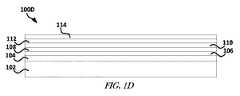
図1Dは、1または複数の実施形態による、その上にエッチング停止層112及び接着層114を備えたデバイス100Cを含むデバイス100Dを図示している。接着層114は、スパッタリングされ得る。接着層114は、例えば銅、チタニウム又はクロム等の金属を含み得る。接着層114によって、そこへの導電性材料の結合を促す媒体を提供できる。図1Eは、1または複数の実施形態による、パターニング材料116(例えばフォトレジスト)がその上に位置付けられたデバイス100Dを含むデバイス100Eを図示している。パターニング材料116は、デバイスの複数の電気的相互接続の形状および範囲を画定するのに役立ち得る。パターニング材料116は、伸長または屈曲できる複数の蛇行相互接続を提供すべくパターニングされ得る。パターニング材料116は、それらの間に形成される複数の相互接続より厚いものであり得る。 FIG. 1D illustrates a device 100D that includes a
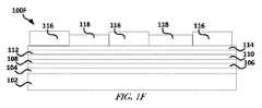
図1Fは、1または複数の実施形態による、導電性材料118がパターニング材料116の間隙に位置付けられたデバイス100Eを含むデバイス100Fを図示している。導電性材料118は、相対的に厚いものであり得る(例えば、厚さ500ナノより大きい)。図1Gは、1または複数の実施形態による、パターニング材料116がそこから除去されたデバイス100Fを含むデバイス100Gを図示している。パターニング材料116は、灰または溶剤を使用して除去され得る。 FIG. 1F illustrates a
図1Hは、1または複数の実施形態による、接着層114、および、エッチング停止層112の一部がそこから除去されたデバイス100Gを含むデバイス100Hを図示している。接着層114は、例えばウェットエッチング又はドライエッチング等によって除去され得る。図1Iは、1または複数の実施形態による、エラストマー材料120がその上に位置付けられたデバイス100Hを含むデバイス100Iを図示している。エラストマー材料120は、導電性材料118をカバーでき、または、導電性材料118を封止するのに役立ち得る。エラストマー材料120によって、エラストマー材料120の外の環境からの保護を提供できる。エラストマー材料120は、屈曲可能で伸縮自在なものであり得る。エラストマー材料120は、例えばエラストマー材料により明確な形状を与えるべく、硬化され得る。エラストマー材料120は、その中に組み込まれるエラストマー材料120の弾性係数未満の弾性係数を有する複数の粒子を含み得る。そのような複数の粒子は、デバイスの中で分散する歪み量に影響を与え得る。1または複数の例において、複数の粒子は、シリカ、又は、エラストマー材料120の弾性係数未満の弾性係数を有する他の材料を含み得る。 FIG. 1H illustrates a device 100H that includes a
図1Jは、1または複数の実施形態による、基板102、及び、酸化物層104がそこから除去されたデバイス100Iを含むデバイス100Jを図示している。基板102および酸化物層104は、例えば酸化物層104を水にさらすことによって、例えばデバイス100Iを水に浸すことによって、除去され得る。図1Kは、1または複数の実施形態による、蒸着物質106、導電性材料108および金属層110がそこから除去されたデバイス100Jを含むデバイス100Kを図示している。蒸着物質106、導電性材料108および金属層110は、例えばそれらをデバイス100Jからドライエッチング又はウェットエッチングすること等によって除去され得る。 FIG. 1J illustrates a device 100J that includes a device 100I from which a
図1Lは、1または複数の実施形態による、エラストマー材料122がその上に位置付けられたデバイス100Kを含むデバイス100Lを図示している。エラストマー材料122は、エラストマー材料120と同じ又は異なる材料を含み得る。エラストマー材料122およびエラストマー材料120は、複数の導電性相互接続(例えば接着層114および導電性材料118を含む複数のコンダクタ)、または、複数の導電性相互接続に電気的に連結される任意の複数のダイ又はコンポーネントを、完全に又は部分的に封止できる。 FIG. 1L illustrates a
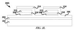
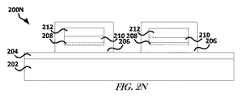
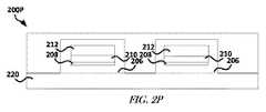
図2A、2B、2C、2D、2E、2F、2G、2H、2I、2J、2K、2L、2M、2N、2Oおよび2Pは、1または複数の実施形態による、薄い導電性相互接続を形成する処理を描いている。 2A, 2B, 2C, 2D, 2E, 2F, 2G, 2H, 2I, 2J, 2K, 2L, 2M, 2N, 2O, and 2P form a thin conductive interconnect according to one or more embodiments. Drawing the process.
図2Aは、1または複数の実施形態による、基板202、及び、基板202上に位置付けられた剥離層204を含むデバイス200Aのブロック図を示している。図2Bは、1または複数の実施形態による、剥離層204上のポリイミド(PI)206を備えたデバイス200Aを含むデバイス200Bのブロック図を示している。PI206はスピンオン(spin on)され得る。PI206は硬化され得る。 FIG. 2A shows a block diagram of a
図2Cは、1または複数の実施形態による、接着層208およびシード層210がその上に位置付けられたデバイス200Bを含むデバイス200Cのブロック図を示している。シード層210は、接着層208に付着する金属を含み得る。接着層208は、例えば銅、チタニウム又はクロム等の金属を含み得る。図2Dは、1または複数の実施形態による、導電性材料212がシード層210上に堆積されたデバイス200Cを含むデバイス200Dのブロック図を示している。導電性材料212は、例えばとりわけ、銅、アルミニウム又は金等の金属、あるいは、他の導電性材料を含み得る。 FIG. 2C shows a block diagram of a
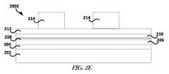
図2Eは、1または複数の実施形態による、フォトレジスト214が導電性材料212上にパターニングされたデバイス200Dを含むデバイス200Eのブロック図を示している。フォトレジスト214は、エッチング処理を実行した後に、導電性材料212が残ることとなる場所を画定できる。フォトレジスト214は、導電性材料212のエッチングを実行した後に、蛇行トレースを生成すべくパターニングされ得る。図2Fは、1または複数の実施形態による、ドライエッチング又はウェットエッチングが実行された後のデバイス200Eを含むデバイス200Fのブロック図を示している。ウェットエッチング又はドライエッチングによって、フォトレジスト214によってカバーされていないシード層210または導電性材料212の複数の部分を除去できる。 FIG. 2E shows a block diagram of a device 200E that includes a device 200D in which a
図2Gは、1または複数の実施形態による、フォトレジスト214がそこから除去されたデバイス200Fを含むデバイス200Gのブロック図を示している。フォトレジスト214は、灰ブラストまたは溶剤を使用して除去され得る。図2Hは、1または複数の実施形態による、接着層208がドライエッチング又はウェットエッチングされたデバイス200Gを含むデバイス200Hのブロック図を示している。エッチングは、接着層208をターゲットにして導電性材料212またはシード層210はターゲットにしない選択的エッチング処理を含み得る。 FIG. 2G shows a block diagram of a
図2Iは、1または複数の実施形態による、他のPI206がそこでスピンオンされたデバイス200Hを含むデバイス200Iのブロック図を示している。PI206は、導電性材料212をカバー(例えば選択的にカバー)すべくスピンオンされ得る。PI206は、複数の蛇行トレース(例えば、エッチング後の接着層208、シード層210および導電性材料212を含む複数のトレース)をカバーすべく配置され得る。PI206は、トレースの場所に関係なくデバイス200Hの大部分をカバーすべく、非選択的にデバイス200Hでスピンオンされ得る。 FIG. 2I shows a block diagram of a device 200I that includes a
図2Jは、1または複数の実施形態による、ハードマスク214がその上に位置付けられたデバイス200Iを含むデバイス200Jのブロック図を示している。ハードマスク214は、複数のPIエッチング処理または材料に耐性があり得る。図2Kは、1または複数の実施形態による、フォトレジスト216がその上の複数のトレース上で選択的にパターニングされたデバイス200Jを含むデバイス200Kのブロック図を示している。フォトレジスト216は、PI206上のハードマスク214、及び、デバイス200Kのトレース上のハードマスク214をハードマスクエッチング処理から保護すべくパターニングされ得る。 FIG. 2J shows a block diagram of a
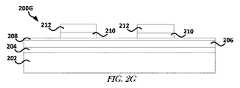
図2Lは、1または複数の実施形態による、ハードマスクエッチングおよびフォトレジスト除去処理を実行した後のデバイス200Kを含むデバイス200Lのブロック図を示している。ハードマスクエッチング処理によって、フォトレジスト216で保護されていないハードマスク214を除去できる。フォトレジスト除去処理によって、フォトレジスト216をデバイス200Lから除去できる。図2Mは、1または複数の実施形態による、PIエッチング処理を実行した後のデバイス200Lを含むデバイス200Mのブロック図を示している。PIエッチング処理によって、ハードマスク214で保護されていないPI206を除去できる。PI206をエッチングすることによって、デバイスの屈曲性または伸縮性を改善できる。これは幾分か、PIの弾性係数がエラストマー材料の弾性係数より大きいことに起因する。 FIG. 2L shows a block diagram of a device
図2Nは、1または複数の実施形態による、ハードマスク214がそこから除去されたデバイス200Mを含むデバイス200Nのブロック図を示している。ハードマスク214は、選択的ドライエッチング又はウェットエッチング処理を使用して除去され得る。図2Oは、1または複数の実施形態による、その上にエラストマー材料218を備えたデバイス200Nを含むデバイス200Oのブロック図を示している。エラストマー材料218によって、その中で少なくとも部分的に位置付けられるトレースに対して屈曲可能で伸縮自在な媒体を提供できる。エラストマー材料218によって、デバイス200Oのコンポーネントに対し、エラストマー材料218の外の環境からの保護を幾らか提供できる。 FIG. 2N shows a block diagram of a
図2Pは、1または複数の実施形態による、基板202および剥離層204がそこから除去され、並びに、他のエラストマー材料220がその上に位置付けられたデバイス200Oを含むデバイス200Pのブロック図を示している。エラストマー材料220は、エラストマー材料218と同じ又は異なるエラストマー材料であり得る。エラストマー材料220およびエラストマー材料218によって、デバイスのトレースを封止(例えば完全に封止)できる。 FIG. 2P shows a block diagram of a
本開示は、柔軟なデバイス(例えば屈曲可能で伸縮自在なデバイス)における複数のメタルラインの成形および剥離に対する、複数の処理フローを示す。厚い導電性材料は、より低い線抵抗、及び、より少ない処理ステップに有利であり得る。薄い導電性材料は、例えば導電性材料がクラック又はブレークすることを防止するのに役立つべく、PIの機械的支持を含み得る。1または複数の実施形態において、PIは複数のトレースだけを(例えば少なくとも部分的に)囲み、これによって、デバイスを柔軟なままにできる。 The present disclosure shows multiple process flows for forming and peeling multiple metal lines in flexible devices (eg, bendable and stretchable devices). A thick conductive material may be advantageous for lower line resistance and fewer processing steps. The thin conductive material may include a mechanical support of PI, for example to help prevent the conductive material from cracking or breaking. In one or more embodiments, the PI surrounds only multiple traces (eg, at least partially), thereby allowing the device to remain flexible.
図3A、3B、3Cおよび3Dは、1または複数実施形態による、コンポーネントをデバイスにワイヤボンディングする処理の複数のブロック図を示している。図3Aは、1または複数の実施形態による、基板302、剥離層304、1または複数のワイヤボンド取り付けパッド306、又は、1または複数のトレース308を含むデバイス300Aのブロック図を示している。複数のトレース308は、例えば、図1Aから1L、または、図2Aから2Pの各々に関して説明される複数の処理を使用して生成できる、複数の厚い又は薄いトレースであり得る。複数のトレース308は、例えば図9A、9B、9Cまたは9Dで示されるように、PIによって、1側面を封止され得、または、2側面を封止され得、或いは、完全に封止され得、もしくは、PIによって全く封止されないものであり得る。 3A, 3B, 3C, and 3D illustrate multiple block diagrams of a process for wire bonding a component to a device, according to one or more embodiments. FIG. 3A shows a block diagram of a
図3Bは、1または複数の実施形態による、コンポーネント314がワイヤ310によって1または複数の結合取り付けパッド306にワイヤボンディングされたデバイス300Aを含むデバイス300Bのブロック図を示している。コンポーネント314は、その上に位置付けされる1または複数の結合パッド312を含み得る。ワイヤ310は、結合取り付けパッド306および結合パッド312に半田付けされ得、そうでなければ、それらに電気的機械的に結合され得る。コンポーネント314は、例えばとりわけ、抵抗器、インダクタ、コンデンサ、トランスフォーマ、磁気デバイス、トランスデューサ、センサ、アンテナ又は検出器等の受動的電気コンポーネント、或いは、例えばとりわけ、トランジスタ、発振器、ダイオード、集積回路(IC)(例えばダイ)、光電子装置、電源等の能動的電気コンポーネントを含み得る。コンポーネントは、例えばとりわけ、端末装置、コネクタ、ケーブルアセンブリ、圧電素子、水晶振動子、共振器、スイッチ、ヒートシンク、又は、ファン等の電気機械的コンポーネントを含み得る。 FIG. 3B shows a block diagram of a device 300B that includes a
図3Cは、1または複数の実施形態による、エラストマー材料316がその上に堆積されたデバイス300Bを含むデバイス300Cのブロック図を示している。エラストマー材料316は、デバイス300Cの複数のアイテムの上または周りに位置付けられ得る。図3Dは、1または複数の実施形態による、基板302および剥離層304がそこから除去され、並びに、エラストマー材料318がその上に位置付けられたデバイス300Cを含むデバイス300Dのブロック図を示している。エラストマー材料316は、エラストマー材料318と同じ又は異なり得る。ワイヤボンディングされたワイヤは、実質的に正味の変化を有さないエラストマー材料と共に、デバイスの弾性係数で伸長および屈曲できる。 FIG. 3C shows a block diagram of a device 300C that includes a device 300B having an
図4は、1または複数の実施形態による、図3Dで「4」をラベリングされた複数の矢印の方向からのデバイス300Dの平面視ブロック図を示している。 FIG. 4 shows a plan view block diagram of
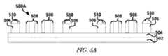
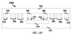
図5A、5B、5Cおよび5Dは、1または複数の実施形態による、フリップチップコンポーネントをデバイスに半田結合する処理の複数のブロック図を示している。図5Aは、1または複数の実施形態による、基板502、剥離層504、1または複数のフリップチップ取り付けパッド506、又は、1または複数のトレース508を含むデバイス500Aのブロック図を示している。複数のトレース508は、例えば図1Aから1L、又は、図2Aから2Pの各々に関して説明される複数の処理を使用して生成できる複数の厚い又は薄いトレースであり得る。半田ボール510は、コンポーネントを取り付けパッド506に半田付けすることを可能にすべく、取り付けパッド506上に位置付けられ得る。複数のトレース508は、例えば図9A、9B、9Cまたは9Dで示されるように、PIによって、1側面を封止され得、または、2側面を封止され得、或いは、完全に封止され得、もしくは、PIによって全く封止されないものであり得る。 5A, 5B, 5C, and 5D illustrate multiple block diagrams of a process for solder bonding a flip chip component to a device, according to one or more embodiments. FIG. 5A shows a block diagram of a device 500A that includes a
図5Bは、1または複数の実施形態による、コンポーネント514が半田ボール510を介して複数の取り付けパッド506の1または複数に半田付けされたデバイス500Aを含むデバイス500Bのブロック図を示している。コンポーネント514は、その上に位置付けられる1または複数の結合パッド512を含み得る。コンポーネント514は、コンポーネント314と同様であり得る。コンポーネント514(又は314)は、屈曲可能であるべく薄いものであり得(例えば厚さ100ミクロン未満)、又は、デバイス500Aの全体的な柔軟性に重大な影響を与えないように寸法付けられ得、または、形付けられ得る。ダイの厚みが減少すると、クラックする前に達成できる曲げ半径が低減される。ダイは、シリコン又は他の半導体を含み得る。ダイは、上に絶縁体および相互接続スタックを含み得る。ダイの裏面は、例えば屈曲する間のダイの構造保全を高めるべく、金属(例えば銅)でコーティングされ得る。 FIG. 5B shows a block diagram of a device 500B that includes a device 500A in which a
図5Cは、1または複数の実施形態による、エラストマー材料516がその上に堆積されたデバイス500Bを含むデバイス500Cのブロック図を示している。エラストマー材料516は、デバイス500Cの複数のアイテムの上または周りに位置付けられ得る。図5Dは、1または複数の実施形態による、基板502および剥離層504がそこから除去され、並びに、エラストマー材料518がその上に位置付けられたデバイス500Cを含むデバイス500Dのブロック図を示している。エラストマー材料516は、エラストマー材料518と同じ又は異なる材料であり得る。 FIG. 5C shows a block diagram of a
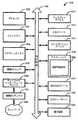
図6は、1または複数の実施形態による、複数のパネルレベル処理のフロー図を示している。図示される処理600は、操作602でエラストマーを堆積する段階と、操作604でトレース材料を積層する段階と、操作606で金属箔タイプを判断する段階と、操作608でトレースリソグラフィを実行する段階と、操作610で金属箔のタイプに応じて上部封止を実行できる段階、操作610、612又は614でトレースエッチングを実行できる段階、又は、操作610又は614で下部封止エッチングを実行できる段階と、操作616でコンポーネントを取り付けできる段階と、操作618でエラストマーを堆積できる段階と、操作620でウェハをパネルから剥離できる段階と、操作622でパッケージを個片化および仕上げできる段階とを含む。 FIG. 6 illustrates a flow diagram for multiple panel level processing according to one or more embodiments. The illustrated
操作602で、エラストマーが、基板上、または、基板上の剥離層上に堆積され得る。トレース材料が、操作604で、エラストマー材料上に積層され得る。金属箔タイプは、例えばトレースが自身の上に、下に、周囲にPIを含む、又は、自身の周りにPIを含まないかどうかであって、606で決定され得る。606での操作は、厚いトレースを使用するか、薄いトレースを使用するか、を判断する段階を含み得る。図9Aで示されるトレースを含むある実施形態において、トレースエッチングが、トレース材料をパターニングすべく実行され得る。図9B又は9Dで示されるトレースを含むある実施形態において、PIが、トレース積層の前に堆積またはエッチングされ得る。図9C又は9Dで示されるトレースを含むある実施形態において、PIが、トレースを覆って堆積されて選択的にエッチングされ得る。 At
操作616でのコンポーネント取り付けは、例えば図3Aから3Dで示されるワイヤボンディング、例えば図5Aから5Dで示されるフリップチップ取り付け、又は、図8Aから8Cで示されるAFC又はACP取り付けを含み得る。操作618で、エラストマーの他の層が、例えばパネルのコンポーネント又はトレースを覆って又はそれらの周りに堆積され得る。620での操作はキャリアパネルのエラストマーを剥ぐ段階を含み得る。620での操作は、化学的または光学的にエラストマーをパネルから剥離する段階を含む。操作622でのパッケージ個片化は、パッケージをパネルからレーザ切断またはのこぎり切断する段階を含み得る。 Component attachment at
図7は、1または複数の実施形態による、パネルレベルデバイス製造処理のフロー図を示している。図示される処理700は、操作702で犠牲材料を堆積する段階と、操作704でトレース材料を積層する段階と、操作706で金属箔タイプを判断する段階と、操作708でトレースリソグラフィを実行する段階と、操作706で決定された金属箔タイプに応じて操作710で上部封止を実行できる段階、操作710、712又は714でトレースエッチングを実行できる段階、又は、操作710又は714で下部封止エッチングを実行できる段階と、操作716でコンポーネントを取り付けできる段階と、操作718でエラストマーを堆積できる段階と、操作720でウェハをパネルから剥離できる段階と、操作722でコンポーネントをデバイスの裏面に取り付けできる段階と、操作724で他のエラストマーを堆積できる段階と、操作726でパッケージを個片化および仕上げできる段階とを含む。 FIG. 7 shows a flow diagram of a panel level device manufacturing process according to one or more embodiments. The illustrated
操作702で、犠牲材料がキャリアパネル上の剥離層上に位置付けられ得る。操作704で、トレース材料が、犠牲材料上に積層され得る。金属箔タイプは、例えばトレースが自身の上に、下に、周囲にPIを含む、又は、自身の周りにPIを含まないかどうかであって、操作706で決定され得る。706での操作は、厚いトレースを使用するか、薄いトレースを使用するか、を判断する段階を含み得る。図9Aで示されるトレースを含むある実施形態において、トレースエッチングが、トレース材料をパターニングすべく実行され得る。図9B又は9Dで示されるトレースを含むある実施形態において、PIが、トレース積層の前に堆積またはエッチングされ得る。図9C又は9Dで示されるトレースを含むある実施形態において、PIが、トレースを覆って堆積されて選択的にエッチングされ得る。 At
操作716でのコンポーネント取り付けは、例えば図3Aから3Dで示されるワイヤボンディング、例えば図5Aから5Dで示されるフリップチップ取り付け、又は、図8Aから8Cで示されるAFC又はACP取り付けを含み得る。操作718で、エラストマーの層が、例えばパネルのコンポーネント又はトレースを覆って又はそれらの周りに堆積され得る。処理700は、ウェハをパネルから剥離した後に犠牲材料を除去する段階を含む。 Component attachment at
720での操作は、剥離剤として犠牲材料を使用する段階、又は、剥離剤上に犠牲材料を配置する段階を含み得る。剥離剤は、パネルとエラストマーとの間における良好な接着を許容され得る。しかしながら、ある一定の温度で(熱剥離の場合)、又は、ある一定の光照射で(例えば光学剥離における紫外線)、剥離剤の複数の接着特性を低減させることができ、剥離剤上のエラストマー又は犠牲材料をパネルから除去できる。もし光学剥離が使用されるならば、パネルは、そこを通過する剥離光に対して透明であり得る(例えば、パネルは、数ある材料の中でも、ガラス又は透明ポリマーを含み得る)。 Operation at 720 may include using a sacrificial material as a release agent, or placing a sacrificial material on the release agent. The release agent can allow good adhesion between the panel and the elastomer. However, at a certain temperature (in the case of thermal exfoliation) or with a certain light irradiation (eg UV in optical exfoliation), the adhesive properties of the release agent can be reduced and the elastomer on the release agent or Sacrificial material can be removed from the panel. If optical stripping is used, the panel can be transparent to stripping light passing therethrough (eg, the panel can include glass or a transparent polymer, among other materials).
722での操作は、犠牲材料に接続されたデバイスの一側面にコンポーネントを取り付ける段階を含み得る。デバイスの当該側面は、操作716でコンポーネントが取り付けられた側面の反対であり得る。724での操作は、操作718で堆積されたエラストマーと同じ又は異なるエラストマーを堆積する段階を含み得る。操作726でのパッケージ個片化は、パッケージをパネルからレーザ切断またはのこぎり切断する段階を含み得る。 Operation at 722 may include attaching the component to one side of the device connected to the sacrificial material. That side of the device may be the opposite of the side where the component was attached in
図8Aは、1または複数の実施形態による、基板キャリア802(例えばパネル又はウェハキャリア)、剥離層804、1または複数の電気的相互接続806、及び、その上に位置付けられる導電性接着材料808を含み得るデバイス800Aのブロック図を示している。導電性接着材料808は、ACF又はACP、或いは、他の液体導電性材料を含み得る。図8Bは、図8Aで「8B」とラベリングされた複数の矢印によって示される視点からデバイス800Aを示している。図8Cは、コンポーネント810が導電性接着材料808に取り付けられた後のデバイス800Aを示している。コンポーネント810は、導電性接着材料808上に位置付けられ得、導電性接着材料808は、その材料を固化してそこにコンポーネント810を取り付けるべく硬化され得る。 FIG. 8A illustrates a substrate carrier 802 (eg, a panel or wafer carrier), a
図9A、9B、9Cおよび9Dは、1または複数の実施形態による、例えば図3Aから3D、4、5Aから5D、又は、8Aから8Cで示されるトレースの一部の複数の平坦な断面図を示している。図9Aは、封止を含まないトレース900Aのブロック図を示している。トレース900Aは、導電性材料902を含み得る。図9Bは、導電性材料902の上面に封止剤904を備えるトレース900Bのブロック図を示している。図9Cは、導電性材料902の底面に封止剤904を備えるトレース900Cのブロック図を示している。図9Dは、導電性材料902の上面および底面に封止剤904を備えるトレース900Dのブロック図を示している。トレースは、トレース全体、又は、トレースの複数の部分だけを囲む封止剤を含み得る。使用される封止剤の量を削減することによって、トレースを含むデバイスの弾性係数を増加させることができる。封止剤は、とりわけ、PI、ポリエチレンテレフタラート(PET)、ポリエチレンナフタレート(PEN)、又は、ポリオレフィン(PO)を含み得る。 9A, 9B, 9C, and 9D illustrate multiple flat cross-sectional views of portions of the traces illustrated, for example, in FIGS. 3A-3D, 4, 5A-5D, or 8A-8C, according to one or more embodiments. Show. FIG. 9A shows a block diagram of a
本明細書で使用されるように、絶縁層またはフォトレジストに対して使用される「堆積」又は「積層」という用語は、様々な方法を意味し得る。一般的なパネルレベル処理は、ドライフィルムラミネーションを含み得る。代替的に、スリットコーティング、ジェットプリンティング(ジェッティング)又は他の方法が使用され得る。本明細書で使用されるように、金属に対する「堆積」又は「積層」という用語は、様々な方法を含み得る。複数の処理は、金属箔積層、スパッタリング、又は、化学的気相成長法(CVD)を含み得る。金属は、例えばサードパーティからのめっき金属を使用することによって、又は、めっき処理を金属に適用することによって、めっきされ得る。 As used herein, the term “deposition” or “stacking” as used for an insulating layer or photoresist may mean various methods. Typical panel level processing may include dry film lamination. Alternatively, slit coating, jet printing (jetting) or other methods can be used. As used herein, the term “deposition” or “stacking” on a metal can include a variety of methods. The plurality of treatments can include metal foil lamination, sputtering, or chemical vapor deposition (CVD). The metal can be plated, for example, by using a plating metal from a third party, or by applying a plating process to the metal.
本明細書で使用されるように、「金属箔」という用語は、露出金属シート、少なくとも一側面を接着剤でコーティングされた金属、または、金属のシートと金属の少なくとも一側面にある絶縁材料とを含む複合材料を含み得る。本明細書で使用されるように、「エッチング」という用語は、複数のパッケージトレースを生成するエッチング方法について言及する。ウェットケミカル処理又はドライエッチング処理が使用され得る。 As used herein, the term “metal foil” refers to an exposed metal sheet, a metal coated with an adhesive on at least one side, or a metal sheet and an insulating material on at least one side of the metal. A composite material comprising As used herein, the term “etching” refers to an etching method that produces a plurality of package traces. Wet chemical processing or dry etching processing may be used.
本明細書で使用されるように、「コンポーネント取り付け」という用語は、複数の受動的または能動的コンポーネントを複数のパッケージトレースに取り付けることについて言及する。複数の例示的コンポーネント取り付け方法は、鉛フリー半田(例えばSnIn, SnBi, SAC305, SnAg, SAC405, SnCu)での半田付けと、異方性導電膜(ACF)、異方性導体ペースト(ACP)、又は、接着性および電気的接続性を許容する複数の導電性有機材料を使用する取り付けと、ワイヤボンディングとを含む。各コンポーネント取り付け処理は、コンポーネント取り付けを可能とすべく追加された処理を含み得る。 As used herein, the term “component attachment” refers to attaching multiple passive or active components to multiple package traces. Several exemplary component mounting methods include lead-free soldering (eg SnIn, SnBi, SAC305, SnAg, SAC405, SnCu), anisotropic conductive film (ACF), anisotropic conductor paste (ACP), Alternatively, it includes attachment using a plurality of conductive organic materials that allow adhesion and electrical connectivity, and wire bonding. Each component attachment process may include a process added to allow component attachment.
本明細書で使用されるように、「ダイ実装/取り付け」という用語は、シリコン、又は、例えばとりわけ、メモリ、マルチチップユニット(MCU)、中央処理装置(CPU)又は無線デバイス(ラジオ)等の他の複数の半導体ダイの取り付けについて言及する。複数の取り付け方法は、ACFによる取り付け(もし複数のACF接合箇所の抵抗がその使用を許容するのであれば)、「コンポーネント取り付け」処理に対して説明される複数の半田材料を使用した半田付け、又は、ワイヤボンディングを含み得る。 As used herein, the term “die mounting / attachment” refers to silicon or, for example, memory, multi-chip unit (MCU), central processing unit (CPU), or wireless device (radio), among others. Reference is made to the attachment of other semiconductor dies. Multiple attachment methods include ACF attachment (if the resistance of multiple ACF junctions allows its use), soldering using multiple solder materials as described for the “component attachment” process, Or it may include wire bonding.
もし受動的または能動的コンポーネントが半田を有さないのであれば、パッケージ製造処理は、例えば図5Aで示される複数の半田バンプでパッケージを形成する半田バンプサブフローを含み得る。既知のパッケージ半田バンプフローが使用され得る。もし受動的または能動的コンポーネントが半田を含むのであれば、半田バンプは必要とされないかもしれない。受動的または能動的コンポーネントは、パッケージに半田付けされ得る。例えば図5Bで示されるように、C4リフロー(C4-reflow)または熱圧着ボンディング(TCB)による半田付けが使用され得る。 If the passive or active component does not have solder, the package manufacturing process may include a solder bump subflow that forms the package with a plurality of solder bumps as shown, for example, in FIG. 5A. Known package solder bump flows can be used. If passive or active components include solder, solder bumps may not be required. Passive or active components can be soldered to the package. For example, as shown in FIG. 5B, soldering by C4 reflow (C4-reflow) or thermocompression bonding (TCB) may be used.
トレースで使用される材料に応じて、トレースのワイヤボンディング領域(例えばトレースに連結されたワイヤボンドパッド)を、トレース金属と異なる金属でカバーすることは有益であり得る。信頼できるワイヤボンドを生成することを可能にすべく、ワイヤボンドパッド上で表面仕上げを生成する処理が使用され得る。そのような処理は、ワイヤボンドパッド精細リソグラフィと、スパッタリング又はめっきすることであり得る(けれど、これらに限定されない)金属堆積とを含み得る。リソグラフィからのフォトレジストは、例えば図3Aで示されるように除去され得る。受動的または能動的コンポーネントは、例えば図3Bで示されるようにパッケージにワイヤボンディングされ得る。 Depending on the material used in the trace, it may be beneficial to cover the wire bonding area of the trace (eg, a wire bond pad coupled to the trace) with a metal different from the trace metal. A process that produces a surface finish on the wire bond pad can be used to allow reliable wire bonds to be generated. Such processing can include wire bond pad fine lithography and metal deposition, which can be (but is not limited to) sputtering or plating. The photoresist from lithography can be removed, for example, as shown in FIG. 3A. Passive or active components can be wire bonded to the package, eg, as shown in FIG. 3B.
ACF処理を使用して、受動的または能動的コンポーネント、又は、パッケージ上の取り付け領域が積層され得る。ACP処理を使用して、例えば図8Aおよび図8Bで示されるように、液体ペーストが、必要とされる場所に噴出され得る。受動的または能動的コンポーネントは、複数のACP領域上に圧縮され得、複数の領域は、例えば図8Cで示されるように決まった場所にコンポーネントを固定すべく硬化され得る。 Using ACF processing, passive or active components or attachment areas on the package can be stacked. Using the ACP process, the liquid paste can be spouted where needed, as shown, for example, in FIGS. 8A and 8B. Passive or active components can be compressed over multiple ACP regions, and the multiple regions can be cured to secure the component in place, for example as shown in FIG. 8C.
複数の異なる取り付け方法の複数の組み合わせは、パネル又はウェハレベル製造処理で使用され得る。 Multiple combinations of different attachment methods can be used in panel or wafer level manufacturing processes.
「エラストマー」という用語は、例えばPDMS、ブチルゴム、Viton(登録商標)、LET7、ポリウレタン、高伸度PI、又は、高伸度ポリエチレンテレフタラート(PET)等の複数の材料について言及する。犠牲材料は、エラストマーから除去できる、例えばとりわけ、PI、PETまたはrevalpha等の材料を含み得る。剥離剤は、実施される剥離処理に応じて、産業上で入手可能な複数の剥離剤から選択され得る。なお、エラストマーとして本明細書で参照される複数の材料は、例えばPI等の屈曲可能な絶縁材料を含み得る。PIは、屈曲可能であって、概して伸縮自在ではない。 The term “elastomer” refers to a plurality of materials such as PDMS, butyl rubber, Viton®, LET7, polyurethane, high elongation PI, or high elongation polyethylene terephthalate (PET). The sacrificial material can include materials that can be removed from the elastomer, such as, among others, PI, PET, or revalpha, among others. The release agent may be selected from a plurality of industrially available release agents depending on the release treatment being performed. Note that the plurality of materials referred to in this specification as the elastomer may include a bendable insulating material such as PI. The PI is bendable and generally not telescopic.
図10は、本明細書で議論されるデバイスを少なくとも部分的に含み得る、又は、当該デバイス上に少なくとも部分的に実装され得る、例示的コンピュータシステム1000機械を図示するブロック図である。コンピュータシステム1000は、コンピューティングデバイスであり得る。ある例において、機械は、スタンドアローンデバイスとして動作し得、他の複数の機械に(例えば携帯電話ネットワークを介して)接続され得る。あるネットワーク化された配備において、機械は、サーバクライアントネットワーク環境においてサーバ機械又はクライアント機械のいずれかの性能で動作し得、又は、複数のピアツーピア(または分散)ネットワーク環境においてピア機械として作用し得る。更に、単一の機械が図示される一方で、「機械」という用語はまた、本明細書で議論される複数の方法論の任意の1または複数を実行する複数の命令の1セット(又は複数のセット)を個々に又は共同で実行する複数の機械の任意のコレクションを含むべく用いられるだろう。 FIG. 10 is a block diagram illustrating an
例示的コンピュータシステム1000は、プロセッサ1002(例えば中央処理装置(CPU)、グラフィック処理ユニット(GPU)、又はその両方)、メインメモリ1004、及び、スタティックメモリ1006を含み得、それらは相互接続1008(例えばリンク、バス等)を介して互いに通信する。コンピュータシステム1000は更に、ビデオディスプレイユニット1010、英数字入力デバイス1012(例えばキーボード)、及び、ユーザインターフェース(UI)ナビゲーションデバイス1014(例えばマウス)を含み得る。ある例において、ビデオディスプレイユニット1010、入力デバイス1012およびUIナビゲーションデバイス1014は、タッチスクリーンディスプレイである。コンピュータシステム1000は、ストレージデバイス1016(例えばドライブユニット)、信号生成デバイス1018(例えばスピーカ)、出力コントローラ1032、電力管理コントローラ1034、ネットワークインターフェースデバイス1020(1または複数のアンテナ1030、トランシーバ、又は、他のワイヤレス通信ハードウェアを含み得、又は、これらと操作可能に通信し得る)、及び、例えばGPSセンサ、コンパス、位置センサ、加速度計または他のセンサ等の1または複数のセンサ1028を追加的に含み得る。複数のアンテナ1030は、ネットワーク1026に連結され得る。システム1000の任意の複数のアイテムは、本明細書で議論されるパネル上に構築された基板を含み得る。 The
複数の例および注記 Multiple examples and notes
本主題は、幾つかの例によって説明され得る。 The subject matter can be illustrated by several examples.
例1は、例えば、(1)第1エラストマー材料をパネル上に堆積すること、(2)トレース材料をエラストマー材料上に積層すること、(3)トレース材料を1または複数のトレースおよび1または複数の結合パッドへとパターニングすべくトレース材料を処理すること、(4)ダイを1または複数の結合パッドに取り付けること、又は、(5)1または複数のトレースおよび1または複数の結合パッドを第1および第2エラストマー材料の中に封止すべく、第2エラストマー材料を1または複数のトレース、結合パッド及びダイの上及び周りに堆積すること、を含み得又は使用し得る等、(例えば、装置、方法、複数の作用を実行する手段、又は、デバイスによって実行された場合にデバイスに複数の作用を実行させ得る複数の命令を含むデバイス可読メモリ等の)主題を含み得又は使用し得る。 Example 1 includes, for example, (1) depositing a first elastomeric material on a panel, (2) laminating a trace material on the elastomeric material, (3) placing the trace material in one or more traces and one or more Processing the trace material to pattern into a bond pad, (4) attaching the die to one or more bond pads, or (5) first mounting one or more traces and one or more bond pads. And depositing the second elastomeric material on and around one or more traces, bond pads and dies to seal within the second elastomeric material, etc. (e.g., device , Methods, means for performing multiple actions, or instructions that, when executed by a device, cause the device to perform multiple actions Vice-readable memory, etc.) may be obtained or used include the subject matter.
例2は、トレース材料を処理することが、約500ナノ未満の厚みを有するトレースを形成すべくトレース材料を処理することを含む、ということを含む又は使用する例1の主題を、含み得又は使用し得、或いは、任意の方法で組み合わされ得る。 Example 2 can include the subject matter of Example 1 including or using that processing the trace material includes processing the trace material to form a trace having a thickness of less than about 500 nanometers, or Can be used or combined in any way.
例3は、トレース材料を第1エラストマー材料上に積層する前に第1トレース封止材料を第1エラストマー材料上に位置付けること、又は、第1トレース封止材料をパターニングすべく第1トレース封止材料の複数の部分を選択的に除去することを含む又は使用する例2の主題を、含み得又は使用し得、或いは、任意の方法で組み合わされ得る。 Example 3 includes positioning the first trace sealing material on the first elastomeric material before laminating the trace material on the first elastomeric material, or first pattern sealing to pattern the first trace sealing material. The subject of Example 2 that includes or uses selectively removing portions of material may be included or used, or may be combined in any manner.
例4は、第2トレース封止材料を1または複数のトレース上に位置付けること、又は、第2トレース封止材料の複数の部分を選択的に除去することを含む又は使用する例3の主題を、含み得又は使用し得、或いは、任意の方法で組み合わされ得る。 Example 4 includes the subject matter of Example 3 including positioning or using a second trace encapsulant over one or more traces, or selectively removing portions of the second trace encapsulant. Can be included, used, or combined in any manner.
例5は、パネルから第1エラストマー材料を剥離すること、又は、第1エラストマー材料を剥離した後に屈曲可能で伸縮自在なデバイスを個片化することを含む又は使用する例1から4の少なくとも1つの主題を、含み得又は使用し得、或いは、任意の方法で組み合わされ得る。 Example 5 includes at least one of Examples 1 to 4 comprising exfoliating or using a first elastomeric material from a panel or singulating a bendable and stretchable device after exfoliating the first elastomeric material. One subject can be included or used, or can be combined in any way.
例6は、トレース材料を処理することが、約500ナノから25ミクロンの間の厚みを有するトレースを形成すべくトレース材料を処理すること含む、ということを含む又は使用する例1又は例5の主題を、含み得又は使用し得、或いは、任意の方法で組み合わされ得る。 Example 6 includes that treating the trace material includes treating or using the trace material to form a trace having a thickness between about 500 nanometers and 25 microns of Example 1 or Example 5 The subject matter can be included or used, or can be combined in any manner.
例7は、コンポーネントを1または複数の結合パッドに取り付けることが、厚さ約10から300ミクロンの間であるダイを取り付けることを含む、ということを含む又は使用する例1から6の少なくとも1つの主題を、含み得又は使用し得、或いは、任意の方法で組み合わされ得る。 Example 7 includes attaching or using a component to one or more bond pads includes attaching a die that is between about 10 to 300 microns in thickness at least one of Examples 1 to 6 The subject matter can be included or used, or can be combined in any manner.
例8は、ダイを1または複数の結合パッドに取り付けることが、ダイを1または複数の結合パッドにワイヤボンディングすることを含む、ということを含む又は使用する例1から7の少なくとも1つの主題を、含み得又は使用し得、或いは、任意の方法で組み合わされ得る。 Example 8 includes at least one subject of Examples 1-7 that includes or uses attaching a die to one or more bond pads includes wire bonding the die to one or more bond pads. Can be included, used, or combined in any manner.
例9は、ダイを1または複数の結合パッドに取り付けることが、ダイを1または複数の結合パッドに半田結合することを含む、ということを含む又は使用する例1から7の少なくとも1つの主題を、含み得又は使用し得、或いは、任意の方法で組み合わされ得る。 Example 9 includes at least one subject of Examples 1-7 that includes or uses attaching a die to one or more bond pads includes solder bonding the die to one or more bond pads. Can be included, used, or combined in any manner.
例10は、例えば、(1)犠牲材料をパネル上に堆積すること、(2)トレース材料を犠牲材料上に積層すること、(3)トレース材料を1または複数のトレースおよび1または複数の結合パッドへとパターニングすべくトレース材料を処理すること、(4)第1ダイを、1または複数の結合パッドの第1側面で1または複数の結合パッドに取り付けること、(5)第1エラストマー材料を、1または複数のトレース、1または複数の結合パッド、及び、第1ダイの上及び周りに堆積すること、(6)パネルから、犠牲材料、1または複数のトレース、1または複数の結合パッド、第1ダイ、及び、第1エラストマー材料を剥離すること、(7)犠牲材料を除去すること、又は、(8)第1および第2エラストマー材料の中で1または複数のトレース及び1または複数の結合パッドを封止すべく、第2エラストマー材料を、1または複数のトレース、1または複数の結合パッド、及び、第1エラストマー材料の上に堆積すること、を含み得又は使用し得る等、(例えば、装置、方法、複数の作用を実行する手段、又は、デバイスによって実行された場合にデバイスに複数の作用を実行させ得る複数の命令を含むデバイス可読メモリ等の)主題を含み得又は使用し得る。 Example 10 includes, for example, (1) depositing a sacrificial material on a panel, (2) laminating a trace material on the sacrificial material, and (3) one or more traces and one or more bonds of the trace material. Processing the trace material to pattern into a pad; (4) attaching a first die to the one or more bond pads on a first side of the one or more bond pads; and (5) a first elastomeric material. Depositing on and around the first die, one or more traces, one or more bond pads, (6) from the panel, sacrificial material, one or more traces, one or more bond pads, Exfoliating the first die and the first elastomer material; (7) removing the sacrificial material; or (8) one or more of the first and second elastomer materials. Depositing a second elastomer material over the one or more traces, the one or more bond pads, and the first elastomer material to seal the race and the one or more bond pads, or Subject matter (e.g., device, method, means for performing multiple actions, or device-readable memory including multiple instructions that, when executed by a device, may cause the device to perform multiple actions) Can be included or used.
例11は、トレース材料を処理することが、約500ナノ未満の厚みを有するトレースを形成すべくトレース材料を処理することを含む、ということを含む又は使用する例10の主題を、含み得又は使用し得、或いは、任意の方法で組み合わされ得る。 Example 11 may include the subject matter of Example 10 including or using processing the trace material includes processing the trace material to form a trace having a thickness of less than about 500 nanometers, or Can be used or combined in any way.
例12は、トレース材料を犠牲材料上に積層する前に第1トレース封止材料を犠牲材料上に位置付けること、又は、第1トレース封止材料をパターニングすべく第1トレース封止材料の複数の部分を選択的に除去することを含む又は使用する例11の主題を、含み得又は使用し得、或いは、任意の方法で組み合わされ得る。 Example 12 includes positioning a first trace sealing material on the sacrificial material before laminating the trace material on the sacrificial material, or a plurality of first trace sealing materials to pattern the first trace sealing material. The subject matter of Example 11 that includes or uses selective removal can be included or used, or can be combined in any manner.
例13は、第2トレース封止材料を1または複数のトレース上に位置付けること、又は、第2トレース封止材料の複数の部分を選択的に除去することを含む又は使用する例12の主題を、含み得又は使用し得、或いは、任意の方法で組み合わされ得る。 Example 13 includes the subject matter of Example 12 including positioning or using a second trace encapsulant over one or more traces, or selectively removing portions of the second trace encapsulant. Can be included, used, or combined in any manner.
例14は、第1エラストマー材料を剥離した後に屈曲可能で伸縮自在なデバイスを個片化することを含む又は使用する例10から13の少なくとも1つの主題を、含み得又は使用し得、或いは、任意の方法で組み合わされ得る。 Example 14 may include or use at least one subject of Examples 10 to 13 comprising or using singulating a bendable and stretchable device after peeling the first elastomeric material, or They can be combined in any way.
例15は、トレース材料を処理することが、約500ナノから25ミクロンの間の厚みを有するトレースを形成すべくトレース材料を処理すること含む、ということを含む又は使用する例10および14の少なくとも1つの主題を、含み得又は使用し得、或いは、任意の方法で組み合わされ得る。 Example 15 includes that processing the trace material includes processing or using the trace material to form a trace having a thickness between about 500 nanometers and 25 microns, at least of Examples 10 and 14 One subject may be included or used, or may be combined in any way.
例16は、第1ダイを1または複数の結合パッドに取り付けることが、厚さ約10から300ミクロンの間であるダイを取り付けることを含む、ということを含む又は使用する例10から15の少なくとも1つの主題を、含み得又は使用し得、或いは、任意の方法で組み合わされ得る。 Example 16 includes attaching or using a first die to one or more bond pads includes attaching a die that is between about 10 to 300 microns in thickness. One subject may be included or used, or may be combined in any way.
例17は、第1ダイを1または複数の結合パッドに取り付けることが、第1ダイを1または複数の結合パッドにワイヤボンディングすることを含む、ということを含む又は使用する例10から16の少なくとも1つの主題を、含み得又は使用し得、或いは、任意の方法で組み合わされ得る。 Example 17 includes, or includes, using attaching a first die to one or more bond pads includes wire bonding the first die to one or more bond pads. One subject may be included or used, or may be combined in any way.
例18は、第1ダイを1または複数の結合パッドに取り付けることが、第1ダイを1または複数の結合パッドに半田結合することを含む、ということを含む又は使用する例10から16の少なくとも1つの主題を、含み得又は使用し得、或いは、任意の方法で組み合わされ得る。 Example 18 includes, or includes, using attaching a first die to one or more bond pads includes solder bonding the first die to one or more bond pads. One subject may be included or used, or may be combined in any way.
例19は、1または複数の結合パッドの第1側面の反対の、1または複数の結合パッドの第2側面で、第2ダイを1または複数の結合パッドのある結合パッドに取り付けることを含む又は使用する例10から18の少なくとも1つの主題を、含み得又は使用し得、或いは、任意の方法で組み合わされ得る。 Example 19 includes attaching a second die to a bond pad with one or more bond pads on a second side of the one or more bond pads opposite the first side of the one or more bond pads, or At least one subject of the examples 10 to 18 used may be included or used, or may be combined in any way.
例20は、例えば、エラストマー基板、エラストマー基板において封止された複数の蛇行トレース、エラストマー基板において封止された複数の結合パッドであり、当該複数の結合パッドの複数の結合パッドは複数の蛇行トレースのある蛇行トレースによって電気的に連結される複数の結合パッド、エラストマー基板の中で封止された約10から300ミクロンの間の厚みを有する屈曲可能な電子ダイ、又は、ダイを複数の結合パッドに連結する複数の電気的結合を含み得又は使用し得る等、(例えば、装置、方法、複数の作用を実行する手段、又は、デバイスによって実行された場合にデバイスに複数の作用を実行させ得る複数の命令を含むデバイス可読メモリ等の)主題を含み得又は使用し得る。 Example 20 is, for example, an elastomer substrate, a plurality of serpentine traces sealed on the elastomer substrate, a plurality of bond pads sealed on the elastomer substrate, and the plurality of bond pads of the plurality of bond pads are a plurality of serpentine traces. A plurality of bond pads electrically connected by a serpentine trace having a thickness, a bendable electronic die having a thickness of between about 10 and 300 microns sealed in an elastomer substrate, or a plurality of bond pads May include or be used with multiple electrical couplings coupled to (e.g., apparatus, method, means for performing multiple actions, or causing a device to perform multiple actions when performed by the device) The subject matter (such as a device readable memory containing a plurality of instructions) may be included or used.
例21は、複数のトレースが厚さ500ナノ未満であり、装置が更に、エラストマーの弾性係数と複数の蛇行トレースの弾性係数との間の弾性係数を備えて複数のトレースを機械的に支持する材料を備える、ということを含む又は使用する例20の主題を、含み得又は使用し得、或いは、任意の方法で組み合わされ得る。 Example 21 is that the plurality of traces are less than 500 nanometers thick, and the device further mechanically supports the plurality of traces with an elastic modulus between that of the elastomer and that of the plurality of serpentine traces. The subject matter of Example 20, including or using comprising material, may be included or used, or may be combined in any manner.
例22は、材料が複数のトレースの2つの両側面に位置付けられる、ということを含む又は使用する例21の主題を、含み得又は使用し得、或いは、任意の方法で組み合わされ得る。 Example 22 may include or use the subject matter of Example 21, including or using that the material is located on two opposite sides of the plurality of traces, or may be combined in any manner.
例23は、材料が複数のトレースの一側面上だけに位置付けられる、ということを含む又は使用する例21の主題を、含み得又は使用し得、或いは、任意の方法で組み合わされ得る。 Example 23 may include or use the subject matter of Example 21, including or using that the material is positioned on only one side of the plurality of traces, or may be combined in any manner.
例24は、材料が複数のトレースを囲む、ということを含む又は使用する例21の主題を、含み得又は使用し得、或いは、任意の方法で組み合わされ得る。 Example 24 may include or use the subject matter of Example 21, including or using that the material surrounds multiple traces, or may be combined in any manner.
例25は、エラストマーがポリジメチルシロキサン(PDMS)を含み、複数のトレースが銅を含む、ということを含む又は使用する例20から24の少なくとも1つの主題を、含み得又は使用し得、或いは、任意の方法で組み合わされ得る。 Example 25 may include or use at least one subject matter of Examples 20 to 24, including or using that the elastomer includes polydimethylsiloxane (PDMS) and the plurality of traces include copper, or They can be combined in any way.
例26は、複数の電気的結合が複数のワイヤボンドを含む、ということを含む又は使用する例20から25の少なくとも1つの主題を、含み得又は使用し得、或いは、任意の方法で組み合わされ得る。 Example 26 may include or use at least one subject matter of Examples 20 to 25 that includes or uses that multiple electrical couplings include multiple wire bonds, or combined in any way. obtain.
例27は、ダイがフリップチップダイであり、複数の電気的結合が複数の半田結合を含む、ということを含む又は使用する例20から25の少なくとも1つの主題を、含み得又は使用し得、或いは、任意の方法で組み合わされ得る。 Example 27 may include or use at least one subject matter of Examples 20 to 25 that includes or uses that the die is a flip chip die and the plurality of electrical bonds includes a plurality of solder bonds, Alternatively, they can be combined in any way.
例28は、複数のワイヤボンドが異方性導体ペースト(ACP)結合または異方性導電膜(ACF)結合を含む、ということを含む又は使用する例20から25の少なくとも1つの主題を、含み得又は使用し得、或いは、任意の方法で組み合わされ得る。 Example 28 includes at least one subject matter of Examples 20 to 25 including or using that the plurality of wire bonds includes anisotropic conductor paste (ACP) bonding or anisotropic conductive film (ACF) bonding. Can be obtained or used, or can be combined in any manner.
例29は、材料がPIを含む、ということを含む又は使用する例21から28の少なくとも1つの主題を、含み得又は使用し得、或いは、任意の方法で組み合わされ得る。 Example 29 may include or use at least one subject of Examples 21 to 28, including or using that the material includes PI, or may be combined in any manner.
例30は、例えば、(1)剥離層を基板上に堆積すること、(2)フォトレジストを剥離層上にパターニングすること、(3)第1導電性材料をパターニングされたフォトレジストと剥離層上との間に位置付けること、(4)フォトレジストを除去すること、(5)第1エラストマーを第1導電性材料の上及び周りに位置付けること、(6)剥離層を剥離すること、(7)第1及び第2エラストマーの間に第1導電性材料を封止すべく、第2エラストマーを第1導電性材料および第1エラストマー上に位置付けること、を含み得又は使用し得る等、(例えば、装置、方法、複数の作用を実行する手段、又は、デバイスによって実行された場合にデバイスに複数の作用を実行させ得る複数の命令を含むデバイス可読メモリ等の)主題を含み得又は使用し得る。 Examples 30 include, for example, (1) depositing a release layer on a substrate, (2) patterning a photoresist on the release layer, and (3) a patterned photoresist and release layer of a first conductive material. (4) removing the photoresist, (5) positioning the first elastomer on and around the first conductive material, (6) peeling the release layer, (7) ) Positioning or using the second elastomer over the first conductive material and the first elastomer to seal the first conductive material between the first and second elastomer, etc. (e.g., Or an apparatus, method, means for performing a plurality of actions, or a device readable memory including a plurality of instructions that, when executed by a device, may cause the device to perform a plurality of actions It may be used.
例31は、フォトレジストをパターニングする前に第2導電性材料を剥離層上にスパッタリングすることを含む又は使用する例30の主題を、含み得又は使用し得、或いは、任意の方法で組み合わされ得る。 Example 31 can include or use the subject matter of Example 30 that includes or uses sputtering a second conductive material onto the release layer prior to patterning the photoresist, or can be combined in any manner. obtain.
例32は、フォトレジストをパターニングする前に、スパッタリングされた第2導電性材料上に第3導電性材料を堆積することを含む又は使用する例31の主題を、含み得又は使用し得、或いは、任意の方法で組み合わされ得る。 Example 32 may include or use the subject matter of Example 31, including or using depositing a third conductive material over the sputtered second conductive material prior to patterning the photoresist, or Can be combined in any way.
例33は、フォトレジストをパターニングする前にエッチング停止接着層を第3導電性材料上に位置付けることを含む又は使用する例32の主題を、含み得又は使用し得、或いは、任意の方法で組み合わされ得る。 Example 33 may include, use, or combine in any manner the subject of Example 32, including or using positioning an etch stop adhesion layer on the third conductive material prior to patterning the photoresist. Can be done.
例34は、第1エラストマーを第1導電性材料の上及び周りに位置付ける前に、第2導電性材料、第3導電性材料および接着層の複数の部分を除去すること、及び、第1エラストマーを第1導電性材料の上及び周りに位置付けることが、第1エラストマーを第1、第2および第3導電性材料の除去されていない複数の部分の上及び周りに位置付けることを含むということ、を含む又は使用する例33の主題を、含み得又は使用し得、或いは、任意の方法で組み合わされ得る。 Example 34 includes removing portions of the second conductive material, the third conductive material, and the adhesive layer prior to positioning the first elastomer over and around the first conductive material, and the first elastomer Positioning on and around the first conductive material includes positioning the first elastomer on and around the unremoved portions of the first, second and third conductive materials; The subject matter of Example 33 can be included or used, or can be combined in any way.
例35は、フォトレジストをパターニングすることが、蛇行トレースパターンで形付けられた第1、第2および第3導電性材料を提供すべくフォトレジストをパターニングすることを含む、ということを含む又は使用する例34の主題を、含み得又は使用し得、或いは、任意の方法で組み合わされ得る。 Example 35 includes or uses that patterning the photoresist includes patterning the photoresist to provide first, second, and third conductive materials shaped with a serpentine trace pattern. The subject matter of Example 34 may be included or used, or may be combined in any manner.
例36は、例えば、(1)剥離層を基板上に堆積すること、(2)第1導電性材料およびエラストマーの弾性係数の間の弾性係数を有する第1材料を剥離層上に位置付けること、(3)第1導電性材料を第1材料上に堆積すること、(4)エッチング耐性材料を第1導電性材料上にパターニングすること、(5)エッチング耐性材料によって保護されていない第1導電性材料の複数の部分を除去すること、(6)エッチング耐性材料を除去すること、(7)第1導電性材料間の複数の場所で第1材料の複数の部分を除去すること、(8)第1エラストマーを第1材料の上及び周りに位置付けること、(9)剥離層を剥離すること、又は、(10)第1および第2エラストマーの間で第1導電性材料および第1材料を封止すべく、第2エラストマーを第1材料および第1エラストマーの上に位置付けること、を含み得又は使用し得る等、(例えば、装置、方法、複数の作用を実行する手段、又は、デバイスによって実行された場合にデバイスに複数の作用を実行させ得る複数の命令を含むデバイス可読メモリ等の)主題を含み得又は使用し得る。 Example 36 includes, for example, (1) depositing a release layer on the substrate, (2) positioning a first material having an elastic modulus between the first conductive material and the elastic modulus of the elastomer on the release layer; (3) depositing a first conductive material on the first material; (4) patterning an etch resistant material on the first conductive material; and (5) a first conductivity not protected by the etch resistant material. Removing a plurality of portions of the conductive material; (6) removing the etch resistant material; (7) removing a plurality of portions of the first material at a plurality of locations between the first conductive materials; ) Positioning the first elastomer over and around the first material, (9) peeling the release layer, or (10) placing the first conductive material and the first material between the first and second elastomers. 2nd elast to seal Positioning on the first material and the first elastomer, etc. may be included or used (e.g., apparatus, method, means for performing multiple actions, or on the device when performed by the device) The subject matter (such as a device readable memory that includes multiple instructions that may cause multiple actions to be performed) may be included or used.
例37は、第1材料の複数の部分を除去する前に、第1導電性材料および第1エラストマーの弾性係数の間の弾性係数を有する第2材料を第1材料および第1導電性材料の上に位置付けることを含む又は使用する例36の主題を、含み得又は使用し得、或いは、任意の方法で組み合わされ得る。 Example 37 illustrates that prior to removing portions of the first material, a second material having an elastic modulus between the elastic modulus of the first conductive material and the first elastomer is changed to that of the first material and the first conductive material. The subject matter of Example 36 that includes or uses positioning above may be included or used, or may be combined in any manner.
例38は、第1材料の複数の部分を除去することが、マスク材料を第2材料の複数の部分の上に位置付けること、マスクによって保護されていない複数の場所における第1および第2材料の複数の部分を除去すること、及び、マスクを除去することを含む、ということを含む又は使用する例37の主題を、含み得又は使用し得、或いは、任意の方法で組み合わされ得る。 Example 38 includes removing portions of the first material, positioning the mask material over the portions of the second material, of the first and second materials at locations that are not protected by the mask. The subject matter of Example 37 can be included or used, or can be combined in any manner, including or using removing multiple portions and removing a mask.
例39は、第1導電性材料を第1材料上に堆積する前に第2導電性材料を第1材料上に堆積することを含む又は使用する例36から39の少なくとも1つの主題を、含み得又は使用し得、或いは、任意の方法で組み合わされ得る。 Example 39 includes at least one subject matter of Examples 36 to 39 that includes or uses depositing a second conductive material on the first material before depositing the first conductive material on the first material. Can be obtained or used, or can be combined in any manner.
上記の詳細な説明は、詳細な説明の一部を形成する添付の複数の図面の複数の参照を含む。複数の図面は、本明細書で議論される複数の方法、装置およびシステムが実施され得る特定の複数の実施形態を、例示によって示している。これらの実施形態はまた、「複数の例」として本明細書で参照される。そのような複数の例は、示され又は説明される複数の要素に加えて複数の要素を含み得る。しかしながら、複数の本発明者はまた、示され又は説明されるこれらの要素だけが提供される複数の例も熟慮している。更に、複数の本発明者はまた、本明細書で示され又は説明される、ある特定の例(又はその1または複数の態様)に関連して、又は、他の複数の例(又はそれらの1または複数の態様)に関連して、示され又は説明されるこれらの要素(又はそれらの1または複数の態様)の任意の組み合わせ又は置き換えを使用する複数の例も熟慮している。 The above detailed description includes multiple references to the accompanying drawings, which form a part of the detailed description. The drawings illustrate, by way of illustration, specific embodiments in which the methods, apparatus and systems discussed herein can be implemented. These embodiments are also referred to herein as “examples”. Such examples may include a plurality of elements in addition to the elements shown or described. However, the inventors have also contemplated examples where only those elements shown or described are provided. Further, the inventors may also relate to one particular example (or one or more aspects thereof) as shown or described herein, or other examples (or theirs). Also contemplated are examples using any combination or replacement of these elements (or one or more aspects thereof) shown or described in connection with one or more aspects.
本明細書において、「ある(a)」又は「ある(an)」という複数の用語は、複数の特許文献において一般的であるように1または複数を含むべく使用され、「少なくとも1つ」又は「1または複数」の任意の他の例または使用とは無関係である。本明細書において、「又は」という用語は、そうでないことが示されない限りにおいて、非排他的であることについて言及すべく使用され、又は、「A又はB」が、「BでなくA」、「AでなくB」及び「A及びB」を含むように使用される。本明細書において、「含む(including)」及び「において(in which)」という複数の用語は、「含む(comprising)」及び「において(wherein)」という複数の各用語の平易な英語の等価物として使用される。また、以下の特許請求の範囲において、「含む(including)」及び「含む(comprising)」という複数の用語には制約がない。すなわち、ある請求項でそのような用語の後ろにリストされる複数の要素に加えて更に複数の要素を含むシステム、デバイス、物品、組成物または処理が、まだ当該請求項の範囲内に含まれていると見なされる。更に、以下の特許請求の範囲において、「第1」、「第2」及び「第3」等の複数の用語は、単なる複数の符号として使用され、それらの複数のオブジェクトに複数の数値的要件を課すことを意図していない。 In this specification, the terms “a” or “an” are used to include one or more as is common in a plurality of patent documents, and include “at least one” or It is independent of any other example or use of “one or more”. In this specification, the term “or” is used to refer to non-exclusive, unless otherwise indicated, or “A or B” is “A instead of B”, Used to include “B instead of A” and “A and B”. In this specification, the terms "including" and "in which" mean the plain English equivalent of each of the terms "comprising" and "wherein". Used as. Also, in the following claims, the terms “including” and “comprising” are not limited. That is, a system, device, article, composition or process that includes more than one element listed after such term in a claim is still within the scope of the claim. Is considered. Further, in the following claims, a plurality of terms such as “first”, “second”, and “third” are used merely as a plurality of symbols, and a plurality of numerical requirements are applied to the plurality of objects. Not intended to impose.
本明細書で使用されるように、参照番号について言及する際に使用される「―」(ダッシュ)は、先の段落で議論された非排他的な意味において、ダッシュにより示される範囲内の全ての要素の「又は」を意味している。例えば、103A−Bは、103A−103Bが「103Bでなく103A」、「103Aでなく103B」及び「103A及び103B」を含むように、{103A、103B}という範囲における複数の要素の非排他的な「又は」を意味している。 As used herein, “-” (dash) used in referring to a reference number is all within the range indicated by the dash in the non-exclusive sense discussed in the previous paragraph. Means “or” of the element. For example, 103A-B is non-exclusive of multiple elements in the range {103A, 103B} so that 103A-103B includes "103A not 103B", "103B not 103A" and "103A and 103B" Means "or".
上記の説明は、例示することを意図しているのであって、限定的なものではない。例えば、上述で説明された複数の例(又は、それらの1または複数の態様)は、互いに組み合わされて使用され得る。他の複数の実施形態は、例えば当業者が上記の説明を検討する際に使用され得る。要約書は、読者が技術的開示の本質を速やかに確認することを許容する37 C.F.R. §1.72(b)(米国特許法施行規則)に従うべく、提供される。要約書は、それが特許請求の範囲または意味を解釈または限定すべく用いられるのではないという理解のもとに提出される。また、上記の詳細な説明において、本開示を効率化すべく、様々な特徴が共にグループ化されているかもしれない。このことは、未請求の開示された特徴が、いずれの請求項にとっても不可欠であることを意図すると解釈されるべきではない。むしろ、発明の主題は、ある特定の開示された実施形態の全ての特徴よりも少ないところにあってよい。従って、その結果、以下の特許請求の範囲は複数の例又は実施形態として詳細な説明に組み込まれており、各請求項は別個の実施形態として独立して成り立つ。そのような複数の実施形態は、様々な組み合わせ及び置き換えにおいて互いに組み合わせ可能であることが熟慮されている。本発明の範囲は、そのような特許請求の範囲が権利を与えられる等価物の全範囲と共に、添付の特許請求の範囲を参照して決定されるべきである。
[項目1]
第1エラストマー材料をパネル上に堆積する段階と、
トレース材料を上記第1エラストマー材料上に積層する段階と、
上記トレース材料を1または複数のトレース及び1または複数の結合パッドへとパターニングすべく上記トレース材料を処理する段階と、
ダイを上記1または複数の結合パッドに取り付ける段階と、
上記第1エラストマー材料および第2エラストマー材料の中に上記1または複数のトレース及び上記1または複数の結合パッドを封止すべく、上記第2エラストマー材料を、上記1または複数のトレース、上記1または複数の結合パッド、及び、上記ダイの上及び周りに堆積する段階と
を含む、伸縮自在で屈曲可能な装置を製造する方法。
[項目2]
上記トレース材料を処理する段階は、約500ナノメートル未満の厚みを有するトレースを形成すべく上記トレース材料を処理する段階を含む、項目1に記載の方法。
[項目3]
上記トレース材料を上記第1エラストマー材料上に積層する前に第1トレース封止材料を上記第1エラストマー材料上に位置付ける段階と、
上記第1トレース封止材料をパターニングすべく上記第1トレース封止材料の複数の部分を選択的に除去する段階と
を更に含む、項目2に記載の方法。
[項目4]
第2トレース封止材料を上記1または複数のトレース上に位置付ける段階と、
上記第2トレース封止材料の複数の部分を選択的に除去する段階と
を更に含む項目3に記載の方法。
[項目5]
上記パネルから上記第1エラストマー材料を剥離する段階と、
上記第1エラストマー材料を剥離した後に屈曲可能で伸縮自在なデバイスを個片化する段階と
を更に含む項目1に記載の方法。
[項目6]
上記トレース材料を処理する段階は、約500ナノメートルから25マイクロメートルの間の厚みを有するトレースを形成すべく上記トレース材料を処理する段階を含む、項目1に記載の方法。
[項目7]
上記ダイを上記1または複数の結合パッドに取り付ける段階は、厚さ約10から300マイクロメートルの間のダイを取り付ける段階を含む、項目1から6のいずれか一項に記載の方法。
[項目8]
上記ダイを上記1または複数の結合パッドに取り付ける段階は、上記ダイを上記1または複数の結合パッドにワイヤボンディングする段階を含む、項目1から6のいずれか一項に記載の方法。
[項目9]
上記ダイを上記1または複数の結合パッドに取り付ける段階は、上記ダイを1または複数の結合パッドに半田結合する段階を含む、項目1から6のいずれか一項に記載の方法。
[項目10]
犠牲材料をパネル上に堆積する段階と、
トレース材料を上記犠牲材料上に積層する段階と、
上記トレース材料を1または複数のトレースおよび1または複数の結合パッドへとパターニングすべく上記トレース材料を処理する段階と、
第1ダイを上記1または複数の結合パッドの第1側面で上記1または複数の結合パッドに取り付ける段階と、
第1エラストマー材料を上記1または複数のトレース、上記1または複数の結合パッド、及び、上記第1ダイの上及び周りに堆積する段階と、
上記パネルから、上記犠牲材料、上記1または複数のトレース、上記1または複数の結合パッド、上記第1ダイ、及び、上記第1エラストマー材料を剥離する段階と、
上記犠牲材料を除去する段階と、
上記第1エラストマー材料および第2エラストマー材料の中に上記1または複数のトレース及び上記1または複数の結合パッドを封止すべく、上記第2エラストマー材料を、上記1または複数のトレース、上記1または複数の結合パッド、及び、上記第1エラストマー材料の上に堆積する段階と
を含む、伸縮自在で屈曲可能な装置を製造する方法。
[項目11]
上記トレース材料を処理する段階は、約500ナノメートル未満の厚みを有するトレースを形成すべく上記トレース材料を処理する段階を含む、項目10に記載の方法。
[項目12]
上記トレース材料を上記犠牲材料上に積層する前に第1トレース封止材料を上記犠牲材料上に位置付ける段階と、
上記第1トレース封止材料をパターニングすべく上記第1トレース封止材料の複数の部分を選択的に除去する段階と
を更に含む、項目11に記載の方法。
[項目13]
第2トレース封止材料を上記1または複数のトレース上に位置付ける段階と、
上記第2トレース封止材料の複数の部分を選択的に除去する段階と
を更に含む、項目12に記載の方法。
[項目14]
上記第1エラストマー材料を剥離した後に屈曲可能で伸縮自在なデバイスを個片化する段階を更に含む、項目10に記載の方法。
[項目15]
上記トレース材料を処理する段階は、約500ナノメートルから25マイクロメートルの間の厚みを有するトレースを形成すべく上記トレース材料を処理する段階を含む、項目10に記載の方法。
[項目16]
上記第1ダイを上記1または複数の結合パッドに取り付ける段階は、厚さ約10から300マイクロメートルの間のダイを取り付ける段階を含む、項目10から15のいずれか一項に記載の方法。
[項目17]
上記第1ダイを上記1または複数の結合パッドに取り付ける段階は、上記第1ダイを上記1または複数の結合パッドにワイヤボンディングする段階を含む、項目10から15のいずれか一項に記載の方法。
[項目18]
上記第1ダイを上記1または複数の結合パッドに取り付ける段階は、上記第1ダイを上記1または複数の結合パッドに半田結合する段階を含む、項目10から15のいずれか一項に記載の方法。
[項目19]
上記1または複数の結合パッドの上記第1側面の反対の上記1または複数の結合パッドの第2側面で、第2ダイを上記1または複数の結合パッドの結合パッドに取り付ける段階を更に含む、項目10から15のいずれか一項に記載の方法。
[項目20]
エラストマー基板と
上記エラストマー基板において封止される複数の蛇行トレースと、
上記エラストマー基板において封止される複数の結合パッドであり、上記複数の結合パッドの複数の結合パッドは上記複数の蛇行トレースの蛇行トレースによって電気的に連結される複数の結合パッドと、
上記エラストマー基板において封止される約10から300マイクロメートルの間の厚みを有する屈曲可能な電子ダイと、
上記ダイを上記複数の結合パッドに連結する複数の電気的結合と
を備える装置。
[項目21]
上記複数のトレースは、厚さ500ナノメートル未満であり、
上記エラストマーの弾性係数と上記複数の蛇行トレースの弾性係数との間の弾性係数を有し、上記複数のトレースを機械的に支持する材料を更に備える、項目20に記載の装置。
[項目22]
上記材料は、上記複数のトレースの2つの両側面に位置付けられる、項目21に記載の装置。
[項目23]
上記材料は、上記複数のトレースの一側面だけに位置付けられる、項目21に記載の装置。
[項目24]
上記材料は上記複数のトレースを囲む、項目21に記載の装置。
[項目25]
上記エラストマーは、ポリジメチルシロキサン(PDMS)を含み、上記複数のトレースは銅を含む、項目20から24のいずれか一項に記載の装置。
The above description is athan is intended to be illustrative, not limiting. For example, the examples described above (or one or more aspects thereof) may be used in combination with each other. Other embodiments may be used, for example, when one of ordinary skill in the art reviews the above description. The abstract is provided to comply with 37 CFR §1.72 (b) (U.S. Patent Enforcement Regulations) that allows the reader to quickly ascertain the nature of the technical disclosure. The Abstract is submitted with the understanding that it will not be used to interpret or limit the scope or meaning of the claims. Also, in the above detailed description, various features may be grouped together to make the present disclosure efficient. This should not be interpreted as intending that an unclaimed disclosed feature is essential to any claim. Rather, the inventive subject matter may lie in less than all the features of a particular disclosed embodiment. As a result, the following claims are hereby incorporated into the detailed description as examples or embodiments, with each claim standing on its own as a separate embodiment. It is contemplated that such embodiments can be combined with each other in various combinations and substitutions. The scope of the invention should be determined with reference to the appended claims, along with the full scope of equivalents to which such claims are entitled.
[Item 1]
Depositing a first elastomeric material on the panel;
Laminating a trace material on the first elastomeric material;
Processing the trace material to pattern the trace material into one or more traces and one or more bond pads;
Attaching the die to the one or more bond pads;
To seal the one or more traces and the one or more bond pads in the first elastomeric material and the second elastomeric material, the second elastomeric material is attached to the one or more traces, the one or more Depositing a plurality of bond pads and on and around the die;
A method of manufacturing a stretchable and bendable device comprising:
[Item 2]
The method of claim 1, wherein processing the trace material comprises processing the trace material to form a trace having a thickness of less than about 500 nanometers.
[Item 3]
Positioning the first trace sealing material on the first elastomeric material before laminating the trace material on the first elastomeric material;
Selectively removing portions of the first trace sealing material to pattern the first trace sealing material;
The method according to
[Item 4]
Positioning a second trace sealing material on the one or more traces;
Selectively removing a plurality of portions of the second trace sealing material;
The method according to Item 3, further comprising:
[Item 5]
Peeling the first elastomer material from the panel;
Separating the bendable and stretchable device after separating the first elastomeric material;
The method according to item 1, further comprising:
[Item 6]
The method of item 1, wherein processing the trace material comprises processing the trace material to form a trace having a thickness between about 500 nanometers and 25 micrometers.
[Item 7]
7. The method of any one of items 1 to 6, wherein attaching the die to the one or more bond pads comprises attaching a die having a thickness of between about 10 to 300 micrometers.
[Item 8]
7. The method of any one of items 1 to 6, wherein attaching the die to the one or more bond pads comprises wire bonding the die to the one or more bond pads.
[Item 9]
7. The method of any one of the preceding items, wherein attaching the die to the one or more bond pads includes solder bonding the die to the one or more bond pads.
[Item 10]
Depositing a sacrificial material on the panel;
Laminating a trace material on the sacrificial material;
Processing the trace material to pattern the trace material into one or more traces and one or more bond pads;
Attaching a first die to the one or more bond pads at a first side of the one or more bond pads;
Depositing a first elastomeric material on and around the one or more traces, the one or more bond pads, and the first die;
Peeling the sacrificial material, the one or more traces, the one or more bond pads, the first die, and the first elastomeric material from the panel;
Removing the sacrificial material;
To seal the one or more traces and the one or more bond pads in the first elastomeric material and the second elastomeric material, the second elastomeric material is attached to the one or more traces, the one or more Depositing a plurality of bond pads and the first elastomeric material;
A method of manufacturing a stretchable and bendable device comprising:
[Item 11]
11. The method of item 10, wherein processing the trace material includes processing the trace material to form a trace having a thickness of less than about 500 nanometers.
[Item 12]
Positioning a first trace sealing material on the sacrificial material before laminating the trace material on the sacrificial material;
Selectively removing portions of the first trace sealing material to pattern the first trace sealing material;
The method according to item 11, further comprising:
[Item 13]
Positioning a second trace sealing material on the one or more traces;
Selectively removing a plurality of portions of the second trace sealing material;
The method according to item 12, further comprising:
[Item 14]
11. The method of item 10, further comprising singulating the bendable and stretchable device after peeling off the first elastomeric material.
[Item 15]
11. The method of item 10, wherein processing the trace material comprises processing the trace material to form a trace having a thickness between about 500 nanometers and 25 micrometers.
[Item 16]
16. A method according to any one of items 10 to 15, wherein attaching the first die to the one or more bond pads comprises attaching a die having a thickness of between about 10 to 300 micrometers.
[Item 17]
16. The method of any one of items 10 to 15, wherein attaching the first die to the one or more bond pads comprises wire bonding the first die to the one or more bond pads. .
[Item 18]
16. The method of any one of items 10 to 15, wherein attaching the first die to the one or more bond pads includes solder bonding the first die to the one or more bond pads. .
[Item 19]
The method further includes attaching a second die to the bond pad of the one or more bond pads at a second side of the one or more bond pads opposite the first side of the one or more bond pads. The method according to any one of 10 to 15.
[Item 20]
With elastomer substrate
A plurality of serpentine traces sealed in the elastomer substrate;
A plurality of bond pads sealed in the elastomer substrate, wherein the plurality of bond pads of the plurality of bond pads are electrically connected by the serpentine traces of the plurality of serpentine traces;
A bendable electronic die having a thickness of between about 10 and 300 micrometers sealed in the elastomer substrate;
A plurality of electrical couplings connecting the die to the plurality of coupling pads;
A device comprising:
[Item 21]
The plurality of traces are less than 500 nanometers thick;
21. The apparatus of item 20, further comprising a material having a modulus of elasticity between the modulus of elasticity of the elastomer and that of the plurality of serpentine traces and mechanically supporting the plurality of traces.
[Item 22]
Item 22. The device of item 21, wherein the material is positioned on two opposite sides of the plurality of traces.
[Item 23]
The apparatus of item 21, wherein the material is positioned on only one side of the plurality of traces.
[Item 24]
The apparatus of item 21, wherein the material surrounds the plurality of traces.
[Item 25]
25. A device according to any one of items 20 to 24, wherein the elastomer comprises polydimethylsiloxane (PDMS) and the plurality of traces comprises copper.
Claims (7)
Translated fromJapanese第1トレース封止材料を前記第1エラストマー材料上に位置付ける段階と、
トレース材料を前記第1トレース封止材料上に積層する段階と、
前記トレース材料を1または複数のトレース及び1または複数の結合パッドへと蛇行パターニングし、約500ナノメートル未満の厚みを有する前記1または複数のトレースを形成すべく前記トレース材料を処理する段階と、
前記第1トレース封止材料をパターニングすべく前記第1トレース封止材料の複数の部分を選択的に除去する段階と、
第2トレース封止材料を前記1または複数のトレース上に、前記1または複数のトレースの上面及び少なくとも一つの側面が前記第2トレース封止材料により封止されるように位置付ける段階と、
前記第2トレース封止材料の複数の部分を、前記1または複数のトレースの上面及び少なくとも一つの側面が前記第2トレース封止材料により封止されるように選択的に除去する段階と、
ダイを前記第1エラストマー材料上に配設し、ワイヤボンディングにより前記ダイを前記1または複数の結合パッドに取り付ける段階と、
前記第1エラストマー材料および第2エラストマー材料の中に前記第2トレース封止材料、前記1または複数のトレース及び前記1または複数の結合パッドを封止すべく、前記第2エラストマー材料を、前記1または複数のトレース、前記1または複数の結合パッド、及び、前記ダイの上及び周りに堆積する段階とを含み、
前記ダイは、厚さ約10から300マイクロメートルであり、裏面が金属でコーティングされ、
前記第1トレース封止材料及び前記第2トレース封止材料は、前記エラストマー材料の弾性係数と前記トレース材料の弾性係数との間の弾性係数を有し、前記1または複数のトレースを機械的に支持する、
伸縮自在で屈曲可能な装置を製造する方法。Depositing a first elastomeric material on the panel;
Positioning a first trace sealing material on the first elastomeric material;
Laminating a trace material on the first trace encapsulant;
Serpentine patterning the trace material into one or more traces and one or more bond pads and treating the trace material to form the one or more traces having a thickness of less than about 500 nanometers;
Selectively removing portions of the first trace sealing material to pattern the first trace sealing material;
Positioning a second trace sealing material onthe one or more traces such that an upper surface and at least one side of the one or more traces are sealed by the second trace sealing material ;
Selectively removing portions ofthe second trace sealing material such that an upper surface and at least one side of the one or more traces are sealed by the second trace sealing material ;
Disposing a die on the first elastomeric material and attaching the die to the one or more bond padsby wire bonding ;
In order to seal the second trace sealing material, the one or more traces and the one or more bond pads in the first elastomeric material and the second elastomeric material, the second elastomeric material is Or a plurality of traces, the one or more bond pads, and depositing on and around the die,
The die has a thickness of about 10 to 300 micrometers, the back side is coated with metal,
The first trace sealing material and the second trace sealing material have an elastic modulus between an elastic modulus of the elastomeric material and an elastic modulus of the trace material, and mechanically move the one or more traces. To support,
A method of manufacturing a stretchable and bendable device.
前記第1エラストマー材料を剥離した後に屈曲可能で伸縮自在なデバイスを個片化する段階と、
を更に含む請求項1に記載の方法。Peeling the first elastomeric material from the panel;
Separating the bendable and stretchable device after peeling the first elastomeric material;
Furthermore, the process according to claim1 comprising a.
第1トレース封止材料を前記犠牲材料上に位置付ける段階と、
トレース材料を前記第1トレース封止材料上に積層する段階と、
前記トレース材料を1または複数のトレースおよび1または複数の結合パッドへと蛇行パターニングし、約500ナノメートル未満の厚みの前記1または複数のトレースを形成すべく前記トレース材料を処理する段階と、
前記第1トレース封止材料をパターニングすべく前記第1トレース封止材料の複数の部分を選択的に除去する段階と、
第2トレース封止材料を前記1または複数のトレース上に、前記1または複数のトレースの上面及び少なくとも一つの側面が前記第2トレース封止材料により封止されるように位置付ける段階と、
前記第2トレース封止材料の複数の部分を、前記1または複数のトレースの上面及び少なくとも一つの側面が前記第2トレース封止材料により封止されるように選択的に除去する段階と、
第1ダイを前記犠牲材料上に配設し、ワイヤボンディングにより前記第1ダイを前記1または複数の結合パッドの第1側面で前記1または複数の結合パッドに取り付ける段階と、
第1エラストマー材料を前記1または複数のトレース、前記1または複数の結合パッド、及び、前記第1ダイの上及び周りに堆積する段階と、
前記パネルから、前記犠牲材料、前記1または複数のトレース、前記1または複数の結合パッド、前記第1ダイ、及び、前記第1エラストマー材料を剥離する段階と、
前記犠牲材料を除去する段階と、
前記第1エラストマー材料および第2エラストマー材料の中に前記第2トレース封止材料、前記1または複数のトレース及び前記1または複数の結合パッドを封止すべく、前記第2エラストマー材料を、前記1または複数のトレース、前記1または複数の結合パッド、及び、前記第1エラストマー材料の上に堆積する段階とを含み、
前記第1ダイは、厚さ約10から300マイクロメートルであり、裏面が金属でコーティングされ、
前記第1トレース封止材料及び前記第2トレース封止材料は、前記エラストマー材料の弾性係数と前記トレース材料の弾性係数との間の弾性係数を有し、前記1または複数のトレースを機械的に支持する、
伸縮自在で屈曲可能な装置を製造する方法。Depositing a sacrificial material on the panel;
Positioning a first trace sealing material on the sacrificial material;
Laminating a trace material on the first trace encapsulant;
Serpentine patterning the trace material into one or more traces and one or more bond pads and treating the trace material to form the one or more traces having a thickness of less than about 500 nanometers;
Selectively removing portions of the first trace sealing material to pattern the first trace sealing material;
Positioning a second trace sealing material onthe one or more traces such that an upper surface and at least one side of the one or more traces are sealed by the second trace sealing material ;
Selectively removing portions ofthe second trace sealing material such that an upper surface and at least one side of the one or more traces are sealed by the second trace sealing material ;
Disposing a first die on the sacrificial material and attaching the first die to the one or more bond pads on a first side of the one or more bond padsby wire bonding ;
Depositing a first elastomeric material on and around the one or more traces, the one or more bond pads, and the first die;
Peeling the sacrificial material, the one or more traces, the one or more bond pads, the first die, and the first elastomeric material from the panel;
Removing the sacrificial material;
In order to seal the second trace sealing material, the one or more traces and the one or more bond pads in the first elastomeric material and the second elastomeric material, the second elastomeric material is Or depositing a plurality of traces, the one or more bond pads, and the first elastomeric material;
The first die has a thickness of about 10 to 300 micrometers, the back surface is coated with metal,
The first trace sealing material and the second trace sealing material have an elastic modulus between an elastic modulus of the elastomeric material and an elastic modulus of the trace material, and mechanically move the one or more traces. To support,
A method of manufacturing a stretchable and bendable device.
前記第2ダイは、厚さ約10から300マイクロメートルであり、裏面が金属でコーティングされる、請求項3または4に記載の方法。Attaching a second die to the bond pad of the one or more bond pads at a second side of the one or more bond pads opposite the first side of the one or more bond pads;
5. A method according to claim3 or 4 , wherein the second die is about 10 to 300 micrometers thick and the back side is coated with metal.
前記エラストマー基板において封止される屈曲可能な複数の蛇行トレースと、
前記エラストマー基板において封止される複数の結合パッドであり、前記複数の結合パッドの複数の結合パッドは前記複数の蛇行トレースの蛇行トレースによって電気的に連結される複数の結合パッドと、
前記エラストマー基板において全面が封止され、約10から300マイクロメートルの間の厚みを有し、前記複数の結合パッドにワイヤボンディングにより接続され、裏面が金属でコーティングされた屈曲可能な電子ダイと、
前記ダイを前記複数の結合パッドに連結する複数の電気的結合とを備え、
前記複数の蛇行トレースは、厚さ500ナノメートル未満であり、
前記エラストマー基板の弾性係数と前記複数の蛇行トレースの弾性係数との間の弾性係数を有し、前記複数の蛇行トレースを機械的に支持する材料を、前記複数の蛇行トレースの上面及び底面と、少なくとも一つの側面との上に更に備える、伸縮自在で屈曲可能な装置。An elastomer substrate and a plurality of bendable serpentine traces sealed in the elastomer substrate;
A plurality of bond pads sealed in the elastomer substrate, wherein the plurality of bond pads are electrically connected by the serpentine traces of the plurality of serpentine traces;
Wherein the elastomeric substratewhole surface issealed, has a thickness between about 10 and 300 microns,is connected by wire bonding to the plurality of bond pads, an electronic die bendable back surface is coated with a metal,
A plurality of electrical couplings connecting the die to the plurality of coupling pads;
The plurality of serpentine traces is less than 500 nanometers thick;
A material having an elastic coefficient between an elastic coefficient of the elastomer substrate and an elastic coefficient of the plurality of serpentine traces, and mechanically supporting theplurality of serpentine traces; A telescopic and bendable device further comprisingon at least one side .
Applications Claiming Priority (1)
| Application Number | Priority Date | Filing Date | Title |
|---|---|---|---|
| PCT/US2014/046395WO2016007175A1 (en) | 2014-07-11 | 2014-07-11 | Bendable and stretchable electronic devices and methods |
Publications (2)
| Publication Number | Publication Date |
|---|---|
| JP2016527730A JP2016527730A (en) | 2016-09-08 |
| JP6195399B2true JP6195399B2 (en) | 2017-09-13 |
Family
ID=55064633
Family Applications (1)
| Application Number | Title | Priority Date | Filing Date |
|---|---|---|---|
| JP2016533302AActiveJP6195399B2 (en) | 2014-07-11 | 2014-07-11 | Bendable and stretchable electronic device and manufacturing method thereof |
Country Status (9)
| Country | Link |
|---|---|
| US (1) | US10204855B2 (en) |
| EP (1) | EP3172048A4 (en) |
| JP (1) | JP6195399B2 (en) |
| KR (1) | KR101691485B1 (en) |
| CN (1) | CN105431292B (en) |
| BR (1) | BR112015015380A2 (en) |
| SG (1) | SG11201610371TA (en) |
| TW (1) | TWI614815B (en) |
| WO (1) | WO2016007175A1 (en) |
Families Citing this family (15)
| Publication number | Priority date | Publication date | Assignee | Title |
|---|---|---|---|---|
| JP6195399B2 (en) | 2014-07-11 | 2017-09-13 | インテル・コーポレーション | Bendable and stretchable electronic device and manufacturing method thereof |
| TWI592956B (en)* | 2015-06-25 | 2017-07-21 | Wafer Mems Co Ltd | Core inductor production methods |
| US20170344055A1 (en)* | 2016-05-25 | 2017-11-30 | Intel Corporation | Structural brace for electronic circuit with stretchable substrate |
| KR20180058626A (en)* | 2016-11-24 | 2018-06-01 | 주식회사 아모그린텍 | Flat cable manufacturing method |
| CN108538799B (en) | 2017-03-02 | 2024-02-27 | 弗莱克斯有限公司 | Interconnect component and interconnect assembly |
| KR102030235B1 (en)* | 2017-06-15 | 2019-10-10 | 고려대학교 세종산학협력단 | Stretchable Substrate Structure and the Manufacturing Method thereof, Stretchable Display and the Manufacturing Method thereof, and Operating Method of Stretchable Display |
| AU2018345539A1 (en) | 2017-10-03 | 2020-04-16 | Editas Medicine, Inc. | HPV-specific binding molecules |
| EP3773908A1 (en)* | 2018-04-05 | 2021-02-17 | Juno Therapeutics, Inc. | T cell receptors and engineered cells expressing same |
| US10985484B1 (en) | 2018-10-01 | 2021-04-20 | Flex Ltd. | Electronic conductive interconnection for bridging across irregular areas in a textile product |
| FR3087936B1 (en)* | 2018-10-24 | 2022-07-15 | Aledia | ELECTRONIC DEVICE |
| CN109686769B (en)* | 2018-12-25 | 2020-09-08 | 深圳市华星光电技术有限公司 | Stretchable display device and manufacturing method thereof |
| CN112020239B (en)* | 2019-05-29 | 2021-07-27 | 北京梦之墨科技有限公司 | Electronic circuit and electronic circuit manufacturing method |
| TWI798901B (en) | 2021-10-29 | 2023-04-11 | 財團法人工業技術研究院 | Circuit apparatus, manufacturing method thereof, and circuit system |
| TWI815553B (en)* | 2022-07-14 | 2023-09-11 | 友達光電股份有限公司 | Circuit structure |
| US12374482B2 (en)* | 2022-11-30 | 2025-07-29 | Intel Corporation | Carrier chuck comprising a plurality of magnets and methods of forming and using thereof |
Family Cites Families (28)
| Publication number | Priority date | Publication date | Assignee | Title |
|---|---|---|---|---|
| JP3247384B2 (en) | 1994-03-18 | 2002-01-15 | 日立化成工業株式会社 | Semiconductor package manufacturing method and semiconductor package |
| KR20050023442A (en)* | 2002-07-26 | 2005-03-09 | 콸콤 인코포레이티드 | Method for accommodating small minimum die in wire bonded area array packages |
| TWI241000B (en) | 2003-01-21 | 2005-10-01 | Siliconware Precision Industries Co Ltd | Semiconductor package and fabricating method thereof |
| US7057116B2 (en) | 2003-06-02 | 2006-06-06 | Intel Corporation | Selective reference plane bridge(s) on folded package |
| WO2005067044A1 (en) | 2004-01-12 | 2005-07-21 | Infineon Technologies Ag | A method for connecting a die assembly to a substrate in an integrated circuit and a semiconductor device comprising a die assembly |
| JP4527991B2 (en)* | 2004-01-28 | 2010-08-18 | 株式会社日立製作所 | Multi-chip module manufacturing method |
| JP2005311321A (en) | 2004-03-22 | 2005-11-04 | Sharp Corp | SEMICONDUCTOR DEVICE, ITS MANUFACTURING METHOD, AND LIQUID CRYSTAL MODULE AND SEMICONDUCTOR MODULE HAVING THE SEMICONDUCTOR DEVICE |
| CN103646848B (en)* | 2004-06-04 | 2018-06-05 | 伊利诺伊大学评议会 | The method of assembling printable semiconductor elements and manufacture electronic device |
| US8217381B2 (en)* | 2004-06-04 | 2012-07-10 | The Board Of Trustees Of The University Of Illinois | Controlled buckling structures in semiconductor interconnects and nanomembranes for stretchable electronics |
| GB0505826D0 (en) | 2005-03-22 | 2005-04-27 | Uni Microelektronica Ct Vsw | Methods for embedding of conducting material and devices resulting from said methods |
| US20070123963A1 (en) | 2005-11-29 | 2007-05-31 | Peter Krulevitch | Method for producing flexible, stretchable, and implantable high-density microelectrode arrays |
| US7914842B1 (en)* | 2006-02-10 | 2011-03-29 | Second Sight Medical Products, Inc | Method of manufacturing a flexible circuit electrode array |
| EP2064710A4 (en) | 2006-09-06 | 2011-05-04 | Univ Illinois | DEFORMATION-CONTROLLED STRUCTURES IN SEMICONDUCTOR INTERCONNECTS AND NANOMEMBRANES FOR STABLE ELECTRONIC DEVICES |
| US20080188020A1 (en)* | 2007-02-05 | 2008-08-07 | Kuo Wei-Min | Method of LED packaging on transparent flexible film |
| KR100887475B1 (en) | 2007-02-26 | 2009-03-10 | 주식회사 네패스 | Semiconductor package and manufacturing method |
| TW200921873A (en) | 2007-11-09 | 2009-05-16 | Powertech Technology Inc | Chip-to-substrate interconnection device with wire-bonding |
| US8097926B2 (en)* | 2008-10-07 | 2012-01-17 | Mc10, Inc. | Systems, methods, and devices having stretchable integrated circuitry for sensing and delivering therapy |
| JP5646492B2 (en) | 2008-10-07 | 2014-12-24 | エムシー10 インコーポレイテッドMc10,Inc. | Stretchable integrated circuit and device with sensor array |
| WO2010086416A1 (en)* | 2009-01-30 | 2010-08-05 | Imec | Stretchable electronic device |
| WO2010086033A1 (en) | 2009-01-30 | 2010-08-05 | Interuniversitair Microelektronica Centrum Vzw | Stretchable electronic device |
| DE102009031568A1 (en) | 2009-06-29 | 2010-12-30 | Fraunhofer-Gesellschaft zur Förderung der angewandten Forschung e.V. | Method for producing an electronic system, method for producing a free-form surface with such a system, as well as electronic system and free-form surfaces with such a system |
| TWI442530B (en) | 2009-10-14 | 2014-06-21 | Advanced Semiconductor Eng | Package carrier, package structure and process of fabricating package carrier |
| US8569894B2 (en)* | 2010-01-13 | 2013-10-29 | Advanced Semiconductor Engineering, Inc. | Semiconductor package with single sided substrate design and manufacturing methods thereof |
| US8525340B2 (en)* | 2010-06-11 | 2013-09-03 | Premitec, Inc. | Flexible electronic devices and related methods |
| TWI508252B (en) | 2011-11-18 | 2015-11-11 | Iridium Medical Technology Co Ltd | Non-planar chip assembly |
| TWI517274B (en) | 2012-03-21 | 2016-01-11 | 矽品精密工業股份有限公司 | Fabrication method of wafer-scaled semiconductor package and fabrication method of wafer-scaled package substrate thereof |
| US8895864B2 (en)* | 2012-03-30 | 2014-11-25 | Nokia Corporation | Deformable apparatus and method |
| JP6195399B2 (en) | 2014-07-11 | 2017-09-13 | インテル・コーポレーション | Bendable and stretchable electronic device and manufacturing method thereof |
- 2014
- 2014-07-11JPJP2016533302Apatent/JP6195399B2/enactiveActive
- 2014-07-11BRBR112015015380Apatent/BR112015015380A2/ennot_activeApplication Discontinuation
- 2014-07-11WOPCT/US2014/046395patent/WO2016007175A1/enactiveApplication Filing
- 2014-07-11EPEP14873107.8Apatent/EP3172048A4/ennot_activeWithdrawn
- 2014-07-11USUS14/653,033patent/US10204855B2/enactiveActive
- 2014-07-11SGSG11201610371TApatent/SG11201610371TA/enunknown
- 2014-07-11CNCN201480003748.5Apatent/CN105431292B/enactiveActive
- 2014-07-11KRKR1020157017041Apatent/KR101691485B1/ennot_activeExpired - Fee Related
- 2015
- 2015-06-18TWTW104119777Apatent/TWI614815B/enactive
Also Published As
| Publication number | Publication date |
|---|---|
| CN105431292A (en) | 2016-03-23 |
| TWI614815B (en) | 2018-02-11 |
| US20160284630A1 (en) | 2016-09-29 |
| KR20160021071A (en) | 2016-02-24 |
| CN105431292B (en) | 2018-06-08 |
| US10204855B2 (en) | 2019-02-12 |
| EP3172048A4 (en) | 2018-04-18 |
| JP2016527730A (en) | 2016-09-08 |
| SG11201610371TA (en) | 2017-01-27 |
| BR112015015380A2 (en) | 2017-07-11 |
| TW201606880A (en) | 2016-02-16 |
| KR101691485B1 (en) | 2017-01-02 |
| WO2016007175A1 (en) | 2016-01-14 |
| EP3172048A1 (en) | 2017-05-31 |
Similar Documents
| Publication | Publication Date | Title |
|---|---|---|
| JP6195399B2 (en) | Bendable and stretchable electronic device and manufacturing method thereof | |
| TWI705525B (en) | Semiconductor device and manufacturing method thereof | |
| US20170047303A1 (en) | Printable component structure with electrical contact | |
| TW201108335A (en) | Semiconductor device and method of forming dam material around periphery of die to reduce warpage | |
| TW201444037A (en) | Glass flip-chip bonding structure | |
| TWI385736B (en) | Apparatus and methods of forming package-on-package interconnects | |
| JP2004193497A (en) | Chip-size package and manufacturing method thereof | |
| CN103515256B (en) | A method for manufacturing a chip package, a chip package and a wafer level package | |
| CN102709200A (en) | Semiconductor device and method of forming insulating layer disposed over the semiconductor die for stress relief | |
| JP6149877B2 (en) | Apparatus and method for forming hermetic seal on flexible substrate | |
| US12400877B2 (en) | Semiconductor devices with flexible reinforcement structure | |
| JP2024001301A (en) | Structure and method for semiconductor packaging | |
| CN107170715B (en) | Semiconductor packaging structure and manufacturing method thereof | |
| US7517785B2 (en) | Electronic interconnects and methods of making same | |
| CN118173508A (en) | Semiconductor device and method of die attach using adhesive layer comprising graphene-coated core |
Legal Events
| Date | Code | Title | Description |
|---|---|---|---|
| A621 | Written request for application examination | Free format text:JAPANESE INTERMEDIATE CODE: A621 Effective date:20150623 | |
| A131 | Notification of reasons for refusal | Free format text:JAPANESE INTERMEDIATE CODE: A131 Effective date:20160830 | |
| A521 | Request for written amendment filed | Free format text:JAPANESE INTERMEDIATE CODE: A523 Effective date:20161111 | |
| A131 | Notification of reasons for refusal | Free format text:JAPANESE INTERMEDIATE CODE: A131 Effective date:20170404 | |
| A521 | Request for written amendment filed | Free format text:JAPANESE INTERMEDIATE CODE: A523 Effective date:20170704 | |
| TRDD | Decision of grant or rejection written | ||
| A01 | Written decision to grant a patent or to grant a registration (utility model) | Free format text:JAPANESE INTERMEDIATE CODE: A01 Effective date:20170718 | |
| A61 | First payment of annual fees (during grant procedure) | Free format text:JAPANESE INTERMEDIATE CODE: A61 Effective date:20170810 | |
| R150 | Certificate of patent or registration of utility model | Ref document number:6195399 Country of ref document:JP Free format text:JAPANESE INTERMEDIATE CODE: R150 | |
| R250 | Receipt of annual fees | Free format text:JAPANESE INTERMEDIATE CODE: R250 | |
| R250 | Receipt of annual fees | Free format text:JAPANESE INTERMEDIATE CODE: R250 | |
| S111 | Request for change of ownership or part of ownership | Free format text:JAPANESE INTERMEDIATE CODE: R313113 | |
| R350 | Written notification of registration of transfer | Free format text:JAPANESE INTERMEDIATE CODE: R350 | |
| R250 | Receipt of annual fees | Free format text:JAPANESE INTERMEDIATE CODE: R250 | |
| R250 | Receipt of annual fees | Free format text:JAPANESE INTERMEDIATE CODE: R250 | |
| R250 | Receipt of annual fees | Free format text:JAPANESE INTERMEDIATE CODE: R250 | |
| R250 | Receipt of annual fees | Free format text:JAPANESE INTERMEDIATE CODE: R250 |