JP6193623B2 - Polishing method and polishing apparatus - Google Patents
Polishing method and polishing apparatusDownload PDFInfo
- Publication number
- JP6193623B2 JP6193623B2JP2013112087AJP2013112087AJP6193623B2JP 6193623 B2JP6193623 B2JP 6193623B2JP 2013112087 AJP2013112087 AJP 2013112087AJP 2013112087 AJP2013112087 AJP 2013112087AJP 6193623 B2JP6193623 B2JP 6193623B2
- Authority
- JP
- Japan
- Prior art keywords
- polishing
- polishing pad
- amount
- pad
- substrate
- Prior art date
- Legal status (The legal status is an assumption and is not a legal conclusion. Google has not performed a legal analysis and makes no representation as to the accuracy of the status listed.)
- Active
Links
Images


Classifications
- H—ELECTRICITY
- H01—ELECTRIC ELEMENTS
- H01L—SEMICONDUCTOR DEVICES NOT COVERED BY CLASS H10
- H01L21/00—Processes or apparatus adapted for the manufacture or treatment of semiconductor or solid state devices or of parts thereof
- H01L21/02—Manufacture or treatment of semiconductor devices or of parts thereof
- H01L21/04—Manufacture or treatment of semiconductor devices or of parts thereof the devices having potential barriers, e.g. a PN junction, depletion layer or carrier concentration layer
- H01L21/18—Manufacture or treatment of semiconductor devices or of parts thereof the devices having potential barriers, e.g. a PN junction, depletion layer or carrier concentration layer the devices having semiconductor bodies comprising elements of Group IV of the Periodic Table or AIIIBV compounds with or without impurities, e.g. doping materials
- H01L21/30—Treatment of semiconductor bodies using processes or apparatus not provided for in groups H01L21/20 - H01L21/26
- H01L21/302—Treatment of semiconductor bodies using processes or apparatus not provided for in groups H01L21/20 - H01L21/26 to change their surface-physical characteristics or shape, e.g. etching, polishing, cutting
- H01L21/304—Mechanical treatment, e.g. grinding, polishing, cutting
- B—PERFORMING OPERATIONS; TRANSPORTING
- B24—GRINDING; POLISHING
- B24B—MACHINES, DEVICES, OR PROCESSES FOR GRINDING OR POLISHING; DRESSING OR CONDITIONING OF ABRADING SURFACES; FEEDING OF GRINDING, POLISHING, OR LAPPING AGENTS
- B24B37/00—Lapping machines or devices; Accessories
- B24B37/005—Control means for lapping machines or devices
- B24B37/013—Devices or means for detecting lapping completion
Landscapes
- Engineering & Computer Science (AREA)
- Mechanical Engineering (AREA)
- Physics & Mathematics (AREA)
- Condensed Matter Physics & Semiconductors (AREA)
- General Physics & Mathematics (AREA)
- Manufacturing & Machinery (AREA)
- Computer Hardware Design (AREA)
- Microelectronics & Electronic Packaging (AREA)
- Power Engineering (AREA)
- Finish Polishing, Edge Sharpening, And Grinding By Specific Grinding Devices (AREA)
- Mechanical Treatment Of Semiconductor (AREA)
Description
Translated fromJapanese本発明は、半導体ウェハ等の基板を研磨パッドに押圧し、基板と研磨パッドとの相対運動により基板表面の被研磨膜を研磨する研磨方法及び研磨装置に関する。 The present invention relates to a polishing method and a polishing apparatus for pressing a substrate such as a semiconductor wafer against a polishing pad and polishing a film to be polished on the surface of the substrate by relative movement between the substrate and the polishing pad.
近年、半導体デバイスの高集積化・高密度化に伴い、回路の配線がますます微細化し、多層配線の層数も増加している。回路の微細化を図りながら多層配線を実現しようとすると、下側の層の表面凹凸を踏襲しながら段差がより大きくなるので、配線層数が増加するに従って、薄膜形成における段差形状に対する膜被覆性(ステップカバレッジ)が悪くなる。したがって、多層配線するためには、このステップカバレッジを改善し、然るべき過程で平坦化処理しなければならない。また光リソグラフィの微細化とともに焦点深度が浅くなるため、半導体デバイスの表面の凹凸段差が焦点深度以下に収まるように半導体デバイス表面を平坦化処理する必要がある。 In recent years, with higher integration and higher density of semiconductor devices, circuit wiring has become increasingly finer and the number of layers of multilayer wiring has increased. When trying to realize multilayer wiring while miniaturizing the circuit, the step becomes larger while following the surface unevenness of the lower layer, so as the number of wiring layers increases, the film coverage to the step shape in thin film formation (Step coverage) deteriorates. Therefore, in order to carry out multilayer wiring, it is necessary to improve the step coverage and perform a flattening process in an appropriate process. Further, since the depth of focus becomes shallower as the optical lithography becomes finer, it is necessary to planarize the surface of the semiconductor device so that the uneven steps on the surface of the semiconductor device are kept below the depth of focus.
従って、半導体デバイスの製造工程においては、半導体デバイス表面の平坦化技術がますます重要になっている。この平坦化技術のうち、最も重要な技術は、化学的機械研磨(CMP(Chemical Mechanical Polishing))である。この化学的機械研磨は、研磨装置を用いて、シリカ(SiO2)等の砥粒を含んだ研磨液を研磨パッドの研磨面上に供給しつつ半導体ウェハなどの基板を研磨面に摺接させて被研磨膜の研磨を行うものである。Accordingly, in the semiconductor device manufacturing process, a planarization technique for the surface of the semiconductor device is becoming increasingly important. Among the planarization techniques, the most important technique is chemical mechanical polishing (CMP). In this chemical mechanical polishing, a substrate such as a semiconductor wafer is brought into sliding contact with the polishing surface while supplying a polishing liquid containing abrasive grains such as silica (SiO2 ) onto the polishing surface of the polishing pad using a polishing apparatus. Thus, the film to be polished is polished.
この種の研磨装置は、研磨パッドを有する研磨テーブルと、半導体ウェハ等の基板を保持するトップリングとを備えている。一般に、基板の外周縁側には、研磨パッドを押圧するリテーナリングが設けられる。このような研磨装置を用いて基板表面の被研磨膜の研磨を行う場合には、トップリングにより基板を保持しつつ、基板を研磨パッドに対して所定の圧力で押圧する。このとき、研磨パッドに研磨液を供給しつつ、研磨パッドとトップリングとを相対運動させることにより、研磨液の存在下で基板表面の被研磨膜が研磨パッドに摺接し、基板表面の被研磨膜が平坦かつ鏡面に研磨される。 This type of polishing apparatus includes a polishing table having a polishing pad and a top ring that holds a substrate such as a semiconductor wafer. Generally, a retainer ring that presses the polishing pad is provided on the outer peripheral edge side of the substrate. When polishing a film to be polished on the substrate surface using such a polishing apparatus, the substrate is pressed against the polishing pad with a predetermined pressure while the substrate is held by the top ring. At this time, by supplying the polishing liquid to the polishing pad and moving the polishing pad and the top ring relative to each other, the film to be polished on the substrate surface is in sliding contact with the polishing pad in the presence of the polishing liquid, and the surface to be polished The film is polished to a flat and mirror surface.
ここに、例えばIC−1000/SUBA400(二層クロス)からなる研磨パッドを使用した研磨プロセスにおいては、研磨パッド上層(IC−1000)の減耗などによる状態変化により、その研磨性能(研磨レートや研磨プロファイル)が変動する場合があることが知られている。 Here, for example, in a polishing process using a polishing pad made of IC-1000 / SUBA400 (double-layer cloth), the polishing performance (polishing rate and polishing) is changed due to a change in state due to wear of the upper layer (IC-1000) of the polishing pad. It is known that the profile may vary.
図1は、研磨プロセスにおける研磨パッド(IC−1000)の厚さと研磨レートの関係の一例を示すグラフである。図1に示すように、研磨パッドの厚さが薄くなるに従って研磨レートが上昇する。また、図2は、50ミル(mil)、32ミル及び80ミルの厚さの異なる研磨パッド(IC−1000)を使用して基板表面の被研磨膜を研磨した時の基板の半径方向位置に対する無次元研磨レートの一例を示すグラフである。図2に示すように、研磨パッドの厚さが異なると研磨プロファイルも異なる。 FIG. 1 is a graph showing an example of the relationship between the thickness of the polishing pad (IC-1000) and the polishing rate in the polishing process. As shown in FIG. 1, the polishing rate increases as the thickness of the polishing pad decreases. FIG. 2 shows the radial position of the substrate when polishing the polishing film on the substrate surface using polishing pads (IC-1000) having different thicknesses of 50 mil, 32 mil and 80 mil. It is a graph which shows an example of a dimensionless polishing rate. As shown in FIG. 2, the polishing profile varies with the thickness of the polishing pad.
したがって、被研磨膜の研磨量や研磨後のプロファイルが常に一定に保たれるようにするためには、例えば研磨パッドをドレッサによりドレッシングすることによって研磨パッドの厚さが減少(減耗)した時に、研磨パッドの減耗量に合わせて、研磨時間や、研磨圧力等の研磨条件を適宜変える必要がある。 Therefore, in order to keep the polishing amount of the film to be polished and the profile after polishing always constant, for example, when the thickness of the polishing pad is reduced (depleted) by dressing the polishing pad with a dresser, It is necessary to appropriately change the polishing conditions such as the polishing time and the polishing pressure in accordance with the amount of wear of the polishing pad.
従来、このような研磨パッドの状態変化による研磨性能の変動をキャンセルする方法として、ITM(In-line Thickness Monitor)やR−ECM(渦電流モニタ)を用いたCLC(閉ループ制御)などが広く用いられている。 Conventionally, as a method of canceling the fluctuation of the polishing performance due to the change in the state of the polishing pad, CLC (closed loop control) using ITM (In-line Thickness Monitor) or R-ECM (Eddy current monitor) is widely used. It has been.
しかし、ITMを用いたCLCは、半導体ウェハ等の基板の表面状態を計測する毎に、基板を研磨部から取出し洗浄して乾燥させる必要があり、このため、この一連の作業に多大の時間を要し、スループットを低下させる要因となっていた。またR−ECMを用いたCLCは、被研磨膜が金属膜である時にしか適用できず、例えば基板表面の銅膜研磨における基板表面の銅膜を除去した後の2段目の研磨(タッチアップ)では、研磨時間や研磨条件を固定して研磨を行うブラインド(Blind)研磨が依然として行なわれている。このため、研磨パッドの状態変化による研磨性能の変動が基板の研磨結果に反映されて生産性の低下を引き起こしていた。またR−ECMを用いたCLCが適用できる金属膜研磨においても、システムの導入には多大な費用が必要となる。 However, every time a CLC using an ITM measures the surface state of a substrate such as a semiconductor wafer, it is necessary to remove the substrate from the polishing section, dry it, and dry it. In short, it has been a factor of reducing the throughput. CLC using R-ECM can be applied only when the film to be polished is a metal film. For example, the second stage polishing (touch-up) after removing the copper film on the substrate surface in the copper film polishing on the substrate surface. However, blind polishing is still performed in which the polishing time and polishing conditions are fixed. For this reason, a variation in polishing performance due to a change in the state of the polishing pad is reflected in the polishing result of the substrate, causing a reduction in productivity. Also in metal film polishing to which CLC using R-ECM can be applied, introduction of the system requires a great deal of cost.
出願人は、研磨パッド等の摩耗部材の摩耗量を算出して、研磨工程が正常に行われているか否かを判断したり、研磨パッド等の摩耗部材の摩耗量と研磨プロファイルとの相関関係を示す相関データを蓄積することによって、研磨条件を好適に制御したりするようにした研磨装置(特許文献1参照)や、研磨パッドのプロファイルの変化に併せて研磨条件を変更するようにした研磨装置(特許文献2参照)を提案している。 The applicant calculates the wear amount of a wear member such as a polishing pad to determine whether the polishing process is normally performed, or correlates the wear amount of a wear member such as a polishing pad and the polishing profile. The polishing apparatus (see Patent Document 1) that suitably controls the polishing conditions by accumulating the correlation data indicating the above, or the polishing conditions that are changed in accordance with the change in the profile of the polishing pad The apparatus (refer patent document 2) is proposed.
更に、出願人は、研磨パッド交換直後から次回交換までの間の研磨速度と研磨パッドの厚みとの関係を求めておき、実際に測定した研磨パッドの厚さに基づいて次回研磨する基板の研磨処理時間を最適化するようにした基板研磨方法及び装置を提案している(特許文献3参照)。 Further, the applicant obtains the relationship between the polishing speed and the thickness of the polishing pad immediately after the polishing pad replacement until the next replacement, and polishes the substrate to be polished next time based on the actually measured polishing pad thickness. A substrate polishing method and apparatus for optimizing the processing time has been proposed (see Patent Document 3).
ウェハに対するウェハ材料除去速度を測定するステップと、研磨有効性に対するツール状態の影響、例えばツールに対する摩耗、使用による経年変化の影響を明確にするモデルを提供するステップとを有する半導体ウェハの表面平坦化方法が提案されている(特許文献4参照)。 Surface planarization of a semiconductor wafer having steps of measuring the wafer material removal rate for the wafer and providing a model that defines the effect of tool conditions on polishing effectiveness, e.g. wear on the tool, aging effects due to use A method has been proposed (see Patent Document 4).
また、研磨パッドの厚みを計測し、計測された値が所定値以下となった場合に、研磨パッドの寿命が尽きたと判断するようにした研磨パッドの寿命判断方法(特許文献5参照)や、ドレッシング条件を変化させることによって、研磨パッドのプロファイルをコントロールするようにした研磨装置(特許文献6参照)が提案されている。 In addition, the thickness of the polishing pad is measured, and when the measured value is equal to or less than a predetermined value, the polishing pad life determination method for determining that the life of the polishing pad has expired (see Patent Document 5), There has been proposed a polishing apparatus (see Patent Document 6) in which the profile of a polishing pad is controlled by changing dressing conditions.
更に、研磨パッドのドレッシングによるカットレートの変化が起きた時にドレッシング条件を変化させることで、望ましい研磨レートが得られるようにした研磨装置(特許文献7〜9参照)や、研磨パッドの残厚等と研磨レートの実測値との重回帰分析によって作成したモデル式に研磨パッドの残厚の測定値等を代入して研磨レートの予測値を算出し、この研磨レートの予測値が所定範囲内にあるか否かによってプロセス異常を判断するようにした研磨装置(特許文献10参照)が提案されている。 Further, a polishing apparatus (see Patent Documents 7 to 9) that can obtain a desired polishing rate by changing dressing conditions when a change in cut rate due to dressing of the polishing pad occurs, a remaining thickness of the polishing pad, and the like The predicted value of the polishing rate is calculated by substituting the measured value of the remaining thickness of the polishing pad into the model formula created by multiple regression analysis of the measured value of the polishing rate and the measured value of the polishing rate. There has been proposed a polishing apparatus (see Patent Document 10) in which a process abnormality is determined depending on whether or not there is.
しかしながら、上記従来例にあっては、例えば研磨パッドをドレッシングすることによって研磨パッドの厚さが減少(減耗)した時に、研磨パッドの減耗量に合わせて、被研磨膜の膜厚を測定することなく研磨時間を適宜変更することによって、特に基板表面の銅膜を除去した後の2段目の研磨(タッチアップ)等に対応できる、フィードフォワード制御を行うようにしたものではない。 However, in the above conventional example, when the thickness of the polishing pad is reduced (depleted) by dressing the polishing pad, for example, the film thickness of the film to be polished is measured in accordance with the amount of wear of the polishing pad. However, by changing the polishing time appropriately, feedforward control that can cope with the second stage polishing (touch-up) after removing the copper film on the substrate surface is not performed.
本発明は上記事情に鑑みて為されたもので、ITMやR−ECMを用いたCLCと比べて比較的安価で導入でき、被研磨膜の膜厚を測定することなく、特に基板表面の銅膜を除去した後の2段目の研磨(タッチアップ)等に対応できるばかりでなく、ITMを用いたCLCのようにスループットを損なうことも無く、研磨パッドの全寿命を通して、安定した研磨性能で被研磨膜を研磨できるようにした研磨方法及び研磨装置を提供することを目的とする。 The present invention has been made in view of the above circumstances, and can be introduced at a relatively low cost as compared with CLC using ITM or R-ECM. In particular, copper on the substrate surface can be measured without measuring the film thickness of the film to be polished. Not only can it cope with the second stage polishing (touch-up) after removing the film, but it does not impair the throughput as in CLC using ITM, and it has a stable polishing performance throughout the entire life of the polishing pad. An object of the present invention is to provide a polishing method and a polishing apparatus capable of polishing a film to be polished.
上記目的を達成するため、本発明の一参考例に係る研磨方法は、研磨テーブル上の研磨パッドに基板を押圧して基板表面の被研磨膜を研磨する研磨方法であって、既知の研磨パッドの減耗量又は厚さと、当該減耗量又は厚さの研磨パッドで基板を所定の研磨量を研磨するのに要した研磨時間及び当該所定の研磨量、又は基板を所定の研磨時間で研磨したときに得られた研磨量及び当該所定の研磨時間との関係から研磨時間補正用のアルゴリズムを予め作成しておき、被研磨膜の研磨目標値を設定し、研磨に使用される研磨パッドの減耗量又は厚さを測定し、測定された研磨パッドの減耗量又は厚さと前記アルゴリズムから前記研磨目標値に最適な研磨時間を求めた後、前記研磨時間で被研磨膜を研磨することを特徴とする。
ここで、所定の研磨量又は所定の研磨時間とは、研磨時間補正式を求める際に用いる、基準とする研磨量又は研磨時間である。In order to achieve the above object, a polishing method accordingto a reference example of the present invention is a polishing method for polishing a film to be polished on a substrate surface by pressing the substrate against a polishing pad on a polishing table. When the substrate is polished for a predetermined polishing amount and the polishing time and the predetermined polishing amount required for polishing the substrate with the polishing pad of the reduced amount or thickness, and the predetermined polishing amount. A polishing time correction algorithm is created in advance based on the relationship between the polishing amount obtained in this step and the predetermined polishing time, the polishing target value of the film to be polished is set, and the amount of wear of the polishing pad used for polishing Alternatively, the thickness is measured, and after determining the optimum polishing time for the polishing target value from the measured amount of wear or thickness of the polishing pad and the algorithm, the film to be polished is polished by the polishing time. .
Here, the predetermined polishing amount or the predetermined polishing time is a reference polishing amount or polishing time used when determining the polishing time correction formula.
本発明の他の参考例に係る研磨方法は、研磨テーブル上の研磨パッドに基板を押圧して基板表面の被研磨膜を研磨する研磨方法であって、既知の同一研磨パッド上の基板研磨処理枚数又は累積ドレッシング時間と、当該基板研磨処理枚数を処理した研磨パッド又は当該累積ドレッシング時間だけドレッシングされた研磨パッドで、基板を所定の研磨量を研磨するのに要した研磨時間及び当該所定の研磨量、又は基板を所定の研磨時間で研磨したときに得られた研磨量及び当該所定の研磨時間との関係から研磨時間補正用のアルゴリズムを予め作成しておき、被研磨膜の研磨目標値を設定し、同一研磨パッド上の基板研磨処理枚数又は累積ドレッシング時間を計測し、計測された同一研磨パッド上の基板研磨処理枚数又は累積ドレッシング時間と前記アルゴリズムから前記研磨目標値に最適な研磨時間を求め、前記研磨時間で被研磨膜を研磨することを特徴とする。A polishing method accordingto another embodiment of the present invention is a polishing method for polishing a film to be polished on a substrate surface by pressing the substrate against a polishing pad on a polishing table, and is a known substrate polishing process on the same polishing pad. The number of sheets or the cumulative dressing time, the polishing time required to polish the substrate to a predetermined polishing amount, and the predetermined polishing with the polishing pad processed for the number of substrate polishing processes or the polishing pad dressed for the cumulative dressing time An algorithm for correcting the polishing time is created in advance from the relationship between the amount or the polishing amount obtained when the substrate is polished at a predetermined polishing time and the predetermined polishing time, and the polishing target value of the film to be polished is determined. Set, measure the number of substrate polishing treatments or cumulative dressing time on the same polishing pad, and measure the number of substrate polishing treatments or cumulative dressing time on the same polishing pad Determine the optimum polishing time to the polishing target value from the algorithm, characterized by polishing the film by the polishing time.
本発明の研磨装置は、研磨テーブル上の研磨パッドに基板を押圧して基板表面の被研磨膜を研磨する研磨装置において、研磨に使用される研磨パッドの減耗量又は厚さを測定する研磨パッド測定器と、前記研磨パッド測定器で測定した研磨パッドの減耗量又は厚さ及び前記研磨パッドの弾性率を記憶するメモリ部と、前記研磨パッドの弾性率を測定して前記メモリ部に記憶させる弾性率測定器と、既知の研磨パッドの減耗量又は厚さと、当該減耗量又は厚さの研磨パッドで、基板を所定の研磨量を研磨するのに要した研磨時間及び当該所定の研磨量、又は基板を所定の研磨時間で研磨したときに得られた研磨量及び当該所定の研磨時間との関係から予め作成した研磨時間補正用のアルゴリズムを格納する格納部と、前記研磨パッド測定器で測定した研磨パッドの減耗量又は厚さと前記研磨時間補正用のアルゴリズムから研磨目標値に最適な研磨時間を算出する演算部と、を有し、前記演算部は、前記研磨パッドの弾性率を前記研磨時間補正用のアルゴリズムに加えて、前記研磨時間に反映することを特徴とする。The polishing apparatus of the present invention is a polishing pad that measures the wear amount or thickness of a polishing pad used for polishing in a polishing apparatus that presses a substrate against a polishing pad on a polishing table to polish a film to be polished on the surface of the substrate. and measuring device, and a memory unit for storing the depletion amount or thicknessand elastic modulus of the polishing pad of a polishing pad measured by the polishing pad measuring apparatusmeasures the elastic modulus of the polishing pad to be stored in the memory unit The elastic modulus measuring device, the amount of wear or thickness ofthe known polishing pad, the polishing time required to polish the substrate to a predetermined amount of polishing with the polishing pad of the amount of wear or thickness, and the predetermined amount of polishing, Alternatively, a storage unit storing a polishing time correction algorithm created in advance based on the relationship between the polishing amount obtained when the substrate is polished at a predetermined polishing time and the predetermined polishing time, and the polishing pad measuring instrument. And a calculation unit for calculating an optimal polishing time to the polishing target value from depleting the amount or thickness and algorithms for the polishing time correction of the polishing pad,were perforated withthe operation unit, the polishing the elastic modulus of the polishing pad In addition to the algorithm for time correction, it isreflected in thepolishing time .
本発明の研磨方法及び研磨装置によれば、例えば研磨パッドをドレッシングすることによって研磨パッドの厚さが減少(減耗)した時に、研磨パッドの減耗量に合わせて、被研磨膜の膜厚を測定することなく研磨時間を適宜変更して、特に基板表面の銅膜を除去した後の2段目の研磨(タッチアップ)等に対応できる、フィードフォワード制御を行うことができる。しかも、本発明の研磨方法及び研磨装置は、ITMやR−ECMを用いたCLCと比べて比較的安価で導入でき、金属膜及び酸化膜の双方の研磨に適用できるばかりでなく、ITMを用いたCLCのようにスループットを損なうことも無く、研磨パッドの全寿命を通して、安定した研磨性能で被研磨膜を研磨することができる。 According to the polishing method and the polishing apparatus of the present invention, for example, when the thickness of the polishing pad is reduced (depleted) by dressing the polishing pad, the film thickness of the film to be polished is measured in accordance with the amount of wear of the polishing pad. The feedforward control can be performed by appropriately changing the polishing time without doing so, and particularly for the second stage polishing (touch-up) after removing the copper film on the substrate surface. In addition, the polishing method and polishing apparatus of the present invention can be introduced at a relatively low cost compared to CLC using ITM or R-ECM, and can be applied to polishing both metal films and oxide films. The film to be polished can be polished with stable polishing performance over the entire life of the polishing pad without impairing the throughput as in the case of CLC.
以下、本発明の実施形態を図面を参照して説明する。
図3は、本発明の実施形態に係る研磨装置の全体構成を示す模式図である。図3に示すように、研磨装置は、研磨テーブル100と、研磨対象物である半導体ウェハ等の基板Wを保持して研磨テーブル100上の研磨面に押圧するトップリング20とを備えている。Hereinafter, embodiments of the present invention will be described with reference to the drawings.
FIG. 3 is a schematic diagram showing the overall configuration of the polishing apparatus according to the embodiment of the present invention. As shown in FIG. 3, the polishing apparatus includes a polishing table 100 and a
研磨テーブル100は、テーブル軸100aを介してその下方に配置される研磨テーブル回転モータ(図示せず)に連結されており、そのテーブル軸100a周りに回転可能になっている。研磨テーブル100の上面には、研磨パッド101が貼付されており、研磨パッド101の表面101aが基板Wの表面の被研磨膜を研磨する研磨面を構成している。研磨テーブル100の上方には研磨液供給ノズル(図示せず)が設置されており、この研磨液供給ノズルによって研磨テーブル100上の研磨パッド101上に研磨液が供給されるようになっている。 The polishing table 100 is connected to a polishing table rotation motor (not shown) disposed below the table via a table shaft 100a, and is rotatable around the table shaft 100a. A
トップリング20は、トップリングシャフト18に接続されており、このトップリングシャフト18は、上下動機構24によりトップリングヘッド16に対して上下動するようになっている。このトップリングシャフト18の上下動により、トップリングヘッド16に対してトップリング20の全体を上下動させ位置決めするようになっている。トップリングシャフト18は、図示しないトップリング回転モータの駆動により回転するようになっている。トップリングシャフト18の回転により、トップリング20がトップリングシャフト18周りに回転するようになっている。なお、トップリングシャフト18の上端にはロータリージョイント25が取り付けられている。 The
なお、市場で入手できる研磨パッドとしては種々のものがあり、例えば、ロデール社製のSUBA800、IC−1000、IC−1000/SUBA400(二層クロス)、フジミインコーポレイテッド社製のSurfin xxx−5、Surfin 000等がある。SUBA800、Surfin xxx−5、Surfin 000は繊維をウレタン樹脂で固めた不織布であり、IC−1000は硬質の発泡ポリウレタン(単層)である。発泡ポリウレタンは、ポーラス(多孔質)状になっており、その表面に多数の微細なへこみまたは孔を有している。 There are various types of polishing pads available on the market, such as SUBA800, IC-1000, IC-1000 / SUBA400 (double-layer cloth) manufactured by Rodel, Surfin xxx-5 manufactured by Fujimi Incorporated, Surfin 000 etc. SUBA800, Surfin xxx-5, and Surfin 000 are non-woven fabrics in which fibers are hardened with urethane resin, and IC-1000 is a hard foamed polyurethane (single layer). The foamed polyurethane is porous (porous) and has a large number of fine dents or pores on the surface thereof.
トップリング20は、その下面に半導体ウェハなどの基板Wを保持できるようになっている。トップリングヘッド16は、支軸14を中心として旋回可能に構成されており、下面に基板Wを保持したトップリング20は、トップリングヘッド16の旋回により、基板の受取位置から研磨テーブル100の上方に移動される。そして、トップリング20を下降させて基板Wを研磨パッド101の表面(研磨面)101aに押圧する。このとき、トップリング20および研磨テーブル100をそれぞれ回転させ、研磨テーブル100の上方に設けられた研磨液供給ノズル(図示せず)から研磨パッド101上に研磨液を供給する。このように、基板を研磨パッド101の研磨面101aに摺接させて基板Wの表面の被研磨膜を研磨する。 The
トップリングシャフト18およびトップリング20を上下動させる上下動機構24は、軸受26を介してトップリングシャフト18を回転可能に支持するブリッジ28と、ブリッジ28に取り付けられたボールねじ32と、支柱30により支持された支持台29と、支持台29上に設けられたACサーボモータ38とを備えている。サーボモータ38を支持する支持台29は、支柱30を介してトップリングヘッド16に固定されている。 A
ボールねじ32は、サーボモータ38に連結されたねじ軸32aと、このねじ軸32aが螺合するナット32bとを備えている。トップリングシャフト18は、ブリッジ28と一体となって上下動するようになっている。したがって、サーボモータ38を駆動すると、ボールねじ32を介してブリッジ28が上下動し、これによりトップリングシャフト18およびトップリング20が上下動する。研磨装置は、ブリッジ28の下面までの距離、すなわちブリッジ28の位置を検出する位置検出部としての測距センサ70を備えている。この測距センサ70によりブリッジ28の位置を検出することで、トップリング20の位置を検出することができるようになっている。測距センサ70は、ボールねじ32,サーボモータ38とともに上下動機構24を構成している。 The ball screw 32 includes a
なお、測距センサ70は、レーザ式センサ、超音波センサ、過電流式センサ、もしくはリニアスケール式センサであってもよい。また、研磨装置は、測距センサ70、サーボモータ38をはじめとする装置内の各機器を制御する制御部47を備えている。制御部47は、メモリ部47a、格納部47b及び演算部47cを有している。 The
この研磨装置は、研磨パッド101の研磨面101aをドレッシングするドレッシングユニット40を備えている。このドレッシングユニット40は、研磨パッド101の研磨面101aに摺接されるドレッサ50と、ドレッサ50が連結されるドレッサシャフト51と、ドレッサシャフト51の上端に設けられたエアシリンダ53と、ドレッサシャフト51を回転自在に支持する揺動アーム55とを備えている。ドレッサ50の下部はドレッシング部材50aにより構成され、このドレッシング部材50aの下面には針状のダイヤモンド粒子が付着している。エアシリンダ53は、支柱56により支持された支持台57上に配置されており、これらの支柱56は揺動アーム55に固定されている。 This polishing apparatus includes a
揺動アーム55は、図示しないモータに駆動されて、支軸58を中心として旋回するように構成されている。ドレッサシャフト51は、図示しないモータの駆動により回転し、このドレッサシャフト51の回転により、ドレッサ50がドレッサシャフト51周りに回転するようになっている。エアシリンダ53は、ドレッサシャフト51を介してドレッサ50を上下動させ、ドレッサ50を所定の押圧力で研磨パッド101の研磨面101aに押圧する。 The
研磨パッド101の研磨面101aのドレッシングは次のようにして行われる。ドレッサ50は、エアシリンダ53により研磨面101aに押圧され、これと同時に図示しない純水供給ノズルから純水が研磨面101aに供給される。この状態で、ドレッサ50がドレッサシャフト51周りに回転し、ドレッシング部材50aの下面(ダイヤモンド粒子)を研磨面101aに摺接させる。このようにして、ドレッサ50により研磨パッド101が削り取られ、研磨面101aがドレッシングされる。このように、研磨面101aがドレッシングされると、研磨パッド101の厚さが減少(減耗)する。 Dressing of the polishing
この研磨装置には、このドレッサ50を利用して研磨パッド101の減耗量を測定する、研磨パッド測定器としての変位センサ60が備えられている。すなわち、変位センサ(研磨パッド測定器)60は、ドレッシングユニット40の揺動アーム55の上面に設けられ、ドレッサ50の変位を測定する。ドレッサシャフト51には、ターゲットプレート61が固定されており、ドレッサ50の上下動にともなって、ターゲットプレート61が上下動するようになっている。変位センサ60は、このターゲットプレート61を挿通するように配置されており、ターゲットプレート61の変位を測定することによりドレッサ50の変位を測定する。なお、変位センサ60としては、リニアスケール、レーザ式センサ、超音波センサ、もしくは渦電流式センサなどのあらゆるタイプのセンサが用いられる。 This polishing apparatus is provided with a
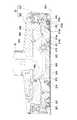
図11(a)及び図11(b)は、変位センサ60、ターゲットプレート61、ドレッサ50、研磨パッド101及び研磨テーブル100の位置関係を示す模式図である。図11(a)は変位センサ60がターゲットプレート61よりも上方に設置されている場合を示す図であり、図11(b)は変位センサ60がターゲットプレート61よりも下方に設置されている場合を示す図である。 FIGS. 11A and 11B are schematic views showing the positional relationship among the
図12(a)及び図12(b)は、垂直方向におけるドレッサ位置(研磨パッドの位置)の測定方向及び測定値を示す模式図である。
図12(a)は、変位センサ60及びターゲットプレート61が図11(a)に示す位置関係にある場合であり、図12(b)は、変位センサ60及びターゲットプレート61が図11(b)に示す位置関係にある場合である。
図12(a)に示すように、変位センサ60がターゲットプレート61よりも上方に設置されている場合には、垂直方向におけるドレッサ位置(研磨パッドの位置)の測定方向は下向きの矢印で表される。ドレッサの基準位置aは、研磨テーブル100上に研磨パッド101が無いときのターゲットプレート61の位置であり、ドレッサの初期位置t0(研磨パッドの初期位置t0)は、研磨パッド101の使用開始時のターゲットプレート61の位置であり、ドレッサの位置t(研磨パッドの位置t)は、研磨パッド101の使用中のターゲットプレート61の位置である。研磨パッドの減耗量は(t−t0)で表され、研磨パッドの初期厚さは(a−t0)で表され、研磨パッドの厚さは(a−t)で表される。FIGS. 12A and 12B are schematic diagrams showing measurement directions and measurement values of the dresser position (position of the polishing pad) in the vertical direction.
12A shows a case where the
As shown in FIG. 12A, when the
図12(b)に示すように、変位センサ60がターゲットプレート61よりも下方に設置されている場合には、垂直方向におけるドレッサ位置(研磨パッドの位置)の測定方向は上向きの矢印で表される。ドレッサの基準位置aは、研磨テーブル100上に研磨パッド101が無いときのターゲットプレート61の位置であり、ドレッサの初期位置t0(研磨パッドの初期位置t0)は、研磨パッド101の使用開始時のターゲットプレート61の位置であり、ドレッサの位置t(研磨パッドの位置t)は、研磨パッド101の使用中のターゲットプレート61の位置である。研磨パッドの減耗量は(t0−t)で表され、研磨パッドの初期厚さは(t0−a)で表され、研磨パッドの厚さは(t−a)で表される。As shown in FIG. 12B, when the
以下に述べる制御方法においては、図11(a)に示すように変位センサ60がターゲットプレート61よりも上方に設置されている場合について述べる。
以下のようにして研磨パッド101の減耗量が測定される。まず、エアシリンダ53を駆動させて、交換後の研磨パッド101の研磨面101aにドレッサ50を当接させる。この状態で、変位センサ60は、ドレッサ50の初期位置(研磨パッドの初期位置t0)を検知する。ドレッサ50の初期位置(研磨パッドの初期位置t0)は、研磨パッド101が研磨テーブル100に貼られていないときのドレッサ垂直方向位置を基準位置としている。研磨パッドの初期位置t0は、垂直方向における研磨パッド101の研磨面101aの位置である。検知したドレッサの初期位置(研磨パッドの初期位置t0)を制御部47のメモリ部47aに記憶する。そして、1つの、または複数の基板の研磨処理が終了し、ドレッサ50により研磨パッド101をドレッシング中、又はドレッシング終了後、ドレッサ50を研磨面101aに当接させた状態でドレッサ50の位置(研磨パッドの位置t)を測定する。研磨パッドの位置tは、垂直方向における研磨パッド101の研磨面101aの位置である。ドレッサ50の位置は、研磨パッド101の摩耗量に応じて下方に変位するため、制御部47は、ドレッサ50の初期位置(研磨パッドの初期位置t0)と研磨及びドレッシング後のドレッサ50の位置(研磨パッドの位置t)との差(t−t0)を求めることで、研磨パッド101の減耗量を求めることができる。このようにして、ドレッサ50の位置を変位センサ60で検知することにより研磨パッド101の減耗量が求められる(図12(a)参照)。In the control method described below, a case where the
The amount of wear of the
なお、この例では、研磨パッド101の減耗量を測定するようにしているが、研磨パッド101の厚さを測定するようにしてもよい。
研磨パッドの厚さは、パッド製造上の誤差により必ずしも均一の初期厚さを有するわけではないので、パッドの初期厚さのバラツキによる影響を取り除くためにも研磨パッドの厚さを計測してフィードフォワード制御を行うことは好ましい。研磨パッド101の厚さを測定するには、研磨パッド101が貼られていない状態の研磨テーブル100の表面にドレッサ50を接触させたときのドレッサ50の垂直方向位置aを変位センサ60により測定する。続いて上述した研磨パッドの減耗量を測定する場合と同様に、研磨パッドの垂直方向初期位置t0及び研磨パッドの垂直方向位置tを測定する。研磨パッドの初期厚さは(a−t0)で表され、研磨パッドの厚さは(a−t)で表される(図12(a)参照)。
研磨パッド101の初期厚さ(a−t0)は制御部47のメモリ部47aに記憶される。In this example, the amount of wear of the
Since the thickness of the polishing pad does not necessarily have a uniform initial thickness due to pad manufacturing errors, the thickness of the polishing pad is measured and fed in order to eliminate the influence of variations in the initial thickness of the pad. It is preferable to perform forward control. To measure the thickness of the
The initial thickness (at−t0 ) of the
次に、図3に示すトップリング20についてより詳細に説明する。図4乃至図7は、トップリング20の断面図であり、複数の半径方向に沿って切断した図である。 Next, the
図4乃至図7に示すように、トップリング20は、基板を研磨面101aに対して押圧するトップリング本体200と、研磨面101aを直接押圧するリテーナリング302とから基本的に構成されている。トップリング本体200は、円盤状の上部材300と、上部材300の下面に取り付けられた中間部材304と、中間部材304の下面に取り付けられた下部材306とを備えている。リテーナリング302は、上部材300の外周部に取り付けられている。上部材300は、ボルト308によりトップリングシャフト18に連結されている。また、中間部材304は、ボルト(図示せず)を介して上部材300に固定されており、下部材306はボルト(図示せず)を介して上部材300に固定されている。上部材300、中間部材304、および下部材306から構成される本体部は、エンジニアリングプラスティック(例えば、PEEK)などの樹脂により形成されている。 As shown in FIGS. 4 to 7, the
下部材306の下面には、基板Wの裏面に当接する弾性膜314が取り付けられている。この弾性膜314は、外周側に配置された環状のエッジホルダ316と、エッジホルダ316の内方に配置された環状のリプルホルダ318,319とによって下部材306の下面に取り付けられている。弾性膜314は、エチレンプロピレンゴム(EPDM)、ポリウレタンゴム、シリコンゴム等の強度および耐久性に優れたゴム材によって形成されている。 An
エッジホルダ316はリプルホルダ318により保持され、リプルホルダ318は複数のストッパ320により下部材306の下面に取り付けられている。リプルホルダ319は複数のストッパ322により下部材306の下面に取り付けられている。 The
図4に示すように、弾性膜314の中央部にはセンター室360が形成されている。リプルホルダ319には、このセンター室360に連通する流路324が形成されており、下部材306には、この流路324に連通する流路325が形成されている。リプルホルダ319の流路324および下部材306の流路325は、図示しない流体供給源に接続されており、加圧された流体が流路325および流路324を通ってセンター室360に供給されるようになっている。 As shown in FIG. 4, a
リプルホルダ318は、弾性膜314のリプル314bおよびエッジ314cをそれぞれ爪部318b,318cで下部材306の下面に押さえつけるようになっており、リプルホルダ319は、弾性膜314のリプル314aを爪部319aで下部材306の下面に押さえつけるようになっている。 The
図5に示すように、弾性膜314のリプル314aとリプル314bとの間には環状のリプル室361が形成されている。弾性膜314のリプルホルダ318とリプルホルダ319との間には隙間314fが形成されており、下部材306にはこの隙間314fに連通する流路342が形成されている。また、中間部材304には、下部材306の流路342に連通する流路344が形成されている。下部材306の流路342と中間部材304の流路344との接続部分には、環状溝347が形成されている。この下部材306の流路342は、環状溝347および中間部材304の流路344を介して図示しない流体供給源に接続されており、加圧された流体がこれらの流路を通ってリプル室361に供給されるようになっている。また、この流路342は、図示しない真空ポンプにも切替可能に接続されており、真空ポンプの作動により弾性膜314の下面に半導体ウェハ等の基板を吸着できるようになっている。 As shown in FIG. 5, an
図6に示すように、リプルホルダ318には、弾性膜314のリプル314bおよびエッジ314cによって形成される環状のアウター室362に連通する流路326が形成されている。また、下部材306には、リプルホルダ318の流路326にコネクタ327を介して連通する流路328が、中間部材304には、下部材306の流路328に連通する流路329がそれぞれ形成されている。このリプルホルダ318の流路326は、下部材306の流路328および中間部材304の流路329を介して図示しない流体供給源に接続されており、加圧された流体がこれらの流路を通ってアウター室362に供給されるようになっている。 As shown in FIG. 6, the
図7に示すように、エッジホルダ316は、弾性膜314のエッジ314dを押さえて下部材306の下面に保持するようになっている。このエッジホルダ316には、弾性膜314のエッジ314cおよびエッジ314dによって形成される環状のエッジ室363に連通する流路334が形成されている。また、下部材306には、エッジホルダ316の流路334に連通する流路336が、中間部材304には、下部材306の流路336に連通する流路338がそれぞれ形成されている。このエッジホルダ316の流路334は、下部材306の流路336および中間部材304の流路338を介して図示しない流体供給源に接続されており、加圧された流体がこれらの流路を通ってエッジ室363に供給されるようになっている。 As shown in FIG. 7, the
このように、この例におけるトップリング20においては、弾性膜314と下部材306との間に形成される圧力室、すなわち、センター室360、リプル室361、アウター室362、およびエッジ室363に供給する流体の圧力を調整することにより、基板を研磨パッド101に押圧する押圧力を基板の部分ごとに調整できるようになっている。 Thus, in the
図8は、図4に示すリテーナリング302の拡大図である。リテーナリング302は、基板の外周縁を保持するものであり、図8に示すように、上部が閉塞された円筒状のシリンダ400と、シリンダ400の上部に取り付けられた保持部材402と、保持部材402によりシリンダ400内に保持される弾性膜404と、弾性膜404の下端部に接続されたピストン406と、ピストン406により下方に押圧されるリング部材408とを備えている。リング部材408の外周面とシリンダ400の下端との間には上下方向に伸縮自在な接続シート420が設けられている。この接続シート420は、リング部材408とシリンダ400との間の隙間を埋めることで研磨液(スラリー)の浸入を防止する役割を持っている。 FIG. 8 is an enlarged view of the
弾性膜314のエッジ(外周縁)314dには、弾性膜314とリテーナリング302とを接続する、上方に屈曲した形状のシール部材422が形成されている。このシール部材422は弾性膜314とリング部材408との隙間を埋めるように配置されており、変形しやすい材料から形成されている。シール部材422は、トップリング本体200とリテーナリング302との相対移動を許容しつつ、弾性膜314とリテーナリング302との隙間に研磨液が浸入してしまうことを防止するために設けられている。この例では、シール部材422は弾性膜314のエッジ314dに一体的に形成されており、断面U字型の形状を有している。 A
ここで、接続シート420やシール部材422を設けない場合は、研磨液がトップリング20内に浸入してしまい、トップリング20を構成するトップリング本体200やリテーナリング302の正常な動作を阻害してしまう。この例によれば、接続シート420やシール部材422によって研磨液のトップリング20への浸入を防止することができ、これによりトップリング20を正常に動作させることができる。なお、弾性膜404、接続シート420、およびシール部材422は、エチレンプロピレンゴム(EPDM)、ポリウレタンゴム、シリコンゴム等の強度および耐久性に優れたゴム材によって形成されている。 Here, when the
リング部材408は、ピストン406に当接する上リング部材408aと、研磨面101aに接触する下リング部材408bとに分割されている。この上リング部材408aの外周面および下リング部材408bの外周面には、周方向に延びるフランジ部がそれぞれ形成されている。これらのフランジ部はクランプ430により把持されており、これにより上リング部材408aと下リング部材408bとが締結されている。このクランプ430はたわみやすい材料から構成されている。クランプ430の初期形状はほぼ直線状であり、クランプ430をリング部材408のフランジ部に取り付けることにより、一部に切り欠きが形成された略環状となる。 The
図8に示すように、保持部材402には、弾性膜404によって形成される室410に連通する流路412が形成されている。また、シリンダ400の上部には、保持部材402の流路412に連通する流路414が形成され、上部材300には、シリンダ400の流路414に連通する流路416が形成されている。この保持部材402の流路412は、シリンダ400の流路414および上部材300の流路416を介して図示しない流体供給源に接続されており、加圧された流体がこれらの流路を通って室410に供給されるようになっている。したがって、室410に供給する流体の圧力を調整することにより、弾性膜404を伸縮させてピストン406を上下動させ、リテーナリング302のリング部材408を所望の圧力で研磨パッド101に押圧することができる。 As shown in FIG. 8, the holding
図示した例では、弾性膜404としてローリングダイヤフラムを用いている。ローリングダイヤフラムは、屈曲した部分をもつ弾性膜からなるもので、ローリングダイヤフラムで仕切る室の内部圧力の変化等により、その屈曲部が転動することにより室の空間を広げることができるものである。室が広がる際にダイヤフラムが外側の部材と摺動せず、ほとんど伸縮しないため、摺動摩擦が極めて少なくてすみ、ダイヤフラムを長寿命化することができ、また、リテーナリング302が研磨パッド101に与える押圧力を精度よく調整することができるという利点がある。 In the illustrated example, a rolling diaphragm is used as the
このような構成により、リテーナリング302のリング部材408だけを下降させることができる。したがって、リテーナリング302のリング部材408が減耗しても、下部材306と研磨パッド101との距離を一定に維持することが可能となる。また、研磨パッド101に接触するリング部材408とシリンダ400とは変形自在な弾性膜404で接続されているため、荷重点のオフセットによる曲げモーメントが発生しない。このため、リテーナリング302による面圧を均一にすることができ、研磨パッド101に対する追従性も向上する。 With such a configuration, only the
図8に示すように、上リング部材408aの内側面には縦方向に延びるV字状溝418が均等に複数形成されている。また、下部材306の外周部には、外方に突出する複数のピン349が設けられており、このピン349がリング部材408のV字状溝418に係合するようになっている。V字状溝418内でリング部材408とピン349が相対的に上下方向にスライド可能になっているとともに、このピン349により上部材300および下部材306を介してトップリング本体200の回転がリテーナリング302に伝達され、トップリング本体200とリテーナリング302は一体となって回転する。このような構成により、弾性膜(ローリングダイヤフラム)404のねじれを防止し、研磨中にリング部材408を研磨面101aに対して円滑に均一に押圧することができる。また弾性膜の寿命を長くすることができる。 As shown in FIG. 8, a plurality of V-shaped
前述のように、弾性膜314のセンター室360、リプル室361、アウター室362、およびエッジ室363に供給する圧力により基板に対する押圧力を制御するので、研磨中には下部材306は研磨パッド101から上方に離れた位置にする必要がある。しかしながら、リテーナリング302が減耗すると、基板と下部材306との間の距離が変化し、弾性膜314の変形の仕方も変わるため、基板に対する面圧分布も変化することになる。このような面圧分布の変化は、プロファイルが不安定になる要因となっていた。 As described above, the pressure applied to the substrate is controlled by the pressure supplied to the
この例では、リテーナリング302を下部材306とは独立して上下動させることができるので、リテーナリング302のリング部材408が減耗しても、基板と下部材306との間の距離を一定に維持することができる。したがって、研磨後の基板のプロファイルを安定化させることができる。 In this example, since the
なお、上述した例では、基板の略全面に弾性膜314が配置されているが、これに限られるものではなく、弾性膜314は基板の少なくとも一部に当接するものであればよい。 In the above-described example, the
ドレッサ50は、ドレッサの下面に付着された針状のダイヤモンド粒子を研磨パッド101に摺接させることで研磨パッド101の研磨面101aを削り取るため、経時的にダイヤモンド粒子が減耗する。ダイヤモンド粒子がある程度減耗すると、研磨面101aの好ましい表面粗さが得られない。その結果、研磨面101aに保持される砥粒の量が少なくなり、正常な研磨工程を行うことができなくなる。 Since the
ここに、単位時間当たりにドレッサ50により削り取られる研磨パッド101の量(以下、カットレートという)は、ドレッサ50の研磨面101aに対する押圧力、およびダイヤモンド粒子の形状に依存する。したがって、ドレッサ50の押圧力が一定の条件下では、ダイヤモンド粒子が減耗するにしたがって、カットレートが少なくなる。この例では、上述した変位センサ60を用いて、カットレート(すなわち、単位時間当たりの研磨面101aの変位)が測定される。 Here, the amount of the
制御部47では、変位センサ60からの出力信号(測定値)に基づき、研磨パッド101のカットレート、すなわち、単位時間当たりの研磨面101aの変位(研磨パッド101の減耗量)が算出される。 The
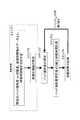
次に、図9を参照して、研磨に使用される研磨パッド101の減耗量を実際に測定し、その情報を基に研磨時間を制御するフィードフォワード制御について説明する。なお、以下の例では、研磨時間補正用のアルゴリズムとして、研磨パッドの実際の減耗量を変数とする二次多項式を使用した例を示している。研磨時間補正用のアルゴリズムとして、研磨パッドの実際の減耗量を変数とする一次多項式、3次以上の多項式、或いは研磨パッドの実際の減耗量と(予定)研磨時間との関係を表した表を使用しても良い。 Next, with reference to FIG. 9, the feedforward control for actually measuring the amount of wear of the
先ず、事前作業として、研磨に使用する研磨パッドと同種の研磨パッドを用いて被研磨膜の研磨を行い研磨後の研磨パッドをドレッシングし、研磨パッドの減耗量を測定する。さらに減耗量測定後の研磨パッドで被研磨膜を所定の研磨量だけ研磨するのに要した研磨時間、又は被研磨膜を所定の研磨時間で研磨したときの研磨量を測定する。このようにして、研磨パッドの減耗量、研磨量及び研磨時間を既知のデータとして少なくとも3セットを準備する。ここで、所定の研磨量又は所定の研磨時間とは、研磨時間補正式を求める際に用いる、基準とする研磨量又は研磨時間である。これらのデータから、研磨パッドの減耗量を変数とする研磨時間補正式を求める(ステップ1)。この既知のデータとしての研磨パッドの減耗量は、研磨パッドの交換直後の初期位置t0と研磨及びドレッシング後の研磨パッドの位置tとの差(t−t0)(既知値)である。既知のデータとしての膜の研磨量は、例えば被研磨膜の初期膜厚THKjと研磨後の最終膜厚THKfとの差(THKj−THKf)であり、既知のデータとしての研磨時間は、被研磨膜を最終膜厚まで研磨するのに要する時間である。First, as a preparatory work, a polishing target film is polished using the same type of polishing pad as that used for polishing, the polished polishing pad is dressed, and the amount of wear of the polishing pad is measured. Further, the polishing time required to polish the film to be polished by a predetermined polishing amount with the polishing pad after the amount of wear is measured, or the polishing amount when the film to be polished is polished for a predetermined polishing time is measured. In this way, at least three sets are prepared with known data on the amount of wear, the amount of polishing, and the polishing time of the polishing pad. Here, the predetermined polishing amount or the predetermined polishing time is a reference polishing amount or polishing time used when determining the polishing time correction formula. From these data, a polishing time correction formula using the amount of wear of the polishing pad as a variable is obtained (step 1). The amount of wear of the polishing pad as the known data is a difference (t−t0 ) (known value) between the initial position t0 immediately after replacement of the polishing pad and the position t of the polishing pad after polishing and dressing. The film polishing amount as known data is, for example, the difference between the initial film thickness THKj of the film to be polished and the final film thickness THKf after polishing (THKj −THKf ), and the polishing time as known data Is the time required to polish the film to be polished to the final film thickness.
つまり、研磨レートPRと、研磨パッドの減耗量(t−t0)との間には、以下の式1の関係があり、研磨時間PTと研磨量PQとの間には、以下の式2の関係がある。
PR=A×(t−t0)2+B×(t−t0)+C (式1)
PT=PQ/PR
=PQ/{A×(t−t0)2+B×(t−t0)+C} (式2)That is, there is a relationship of the following formula 1 between the polishing rate PR and the amount of wear (t−t0 ) of the polishing pad, and the following formula 2 between the polishing time PT and the polishing amount PQ. There is a relationship.
PR = A × (t−t0 )2 + B × (t−t0 ) + C (Formula 1)
PT = PQ / PR
= PQ / {A × (t−t0 )2 + B × (t−t0 ) + C} (Formula 2)
そこで、少なくとも3セットの既知の研磨パッドの減耗量と、既知の研磨量及び既知の研磨時間のデータから、式1の定数A,B及びCを求めることで、研磨パッドの減耗量(t−t0)を変数とする研磨時間補正式(式2)を予め求め、これを制御部47の格納部47bに格納しておく。Therefore, by determining the constants A, B and C of Equation 1 from the data of at least three sets of known polishing pad depletion amount, the known polishing amount and the known polishing time, the depletion amount (t− A polishing time correction formula (Formula 2) with t0 ) as a variable is obtained in advance and stored in the
次に、被研磨膜の研磨目標値を設定し(ステップ2)、この研磨目標値を制御部47のメモリ部47aに記憶しておく。この例では、研磨目標値として、研磨量PQ(設定値)を直接設定するようにしている。研磨後の被研磨膜の最終膜厚を研磨目標値としてもよく、この場合、被研磨膜の初期膜厚から最終膜厚を差し引くことで研磨量を求めることができる。被研磨膜の初期膜厚は、研磨装置に設置した膜厚センサ(図示せず)で測定するか、または外部で予め測定したデータを取り込むことによって得られる。この段階で事前準備が完了する。 Next, a polishing target value of the film to be polished is set (step 2), and this polishing target value is stored in the
一方、研磨装置にあっては、前述のように、ドレッサ50の初期位置を測定することにより、交換直後の研磨パッド101の初期位置t0(実測値)を測定し、この研磨パッド101の初期位置t0(実測値)を制御部47のメモリ部47aに記憶しておく。そして、実際に基板を研磨し、ドレッサ50により研磨パッド101をドレッシング中、又はドレッシング終了後、研磨パッド101の位置t(実測値)を、例えば一定周期で測定し、メモリ部47aに記憶しておいた研磨パッド101の初期位置t0(実測値)との差から研磨パッド101の減耗量(t−t0)(実測値)を測定する(ステップ3)。On the other hand, in the polishing apparatus, as described above, the initial position t0 (actual value) of the
次に、予め定数A、B及びCを求めて格納部47bに格納しておいた、前述の研磨時間補正式(式2)を演算部47cに引き出し、この式2に研磨目標値としての研磨量PQ(設定値)と、実際に測定した研磨パッドの減耗量(t−t0)(実測値)とをそれぞれ代入して、研磨時間PTを求める(ステップ4)。Next, constants A, B, and C are obtained in advance and stored in the
そして、ステップ4で得られた研磨時間PTを反映させて研磨装置による被研磨膜の研磨を行う(ステップ5)。これにより、研磨パッド101をドレッシングすることによって研磨パッド101の厚さが減少(減耗)した時に、研磨パッド101の減耗量に合わせて研磨時間を適宜変更するフィードフォワード制御を行うことができる。 Then, the polishing film is polished by the polishing apparatus while reflecting the polishing time PT obtained in step 4 (step 5). Thus, when the thickness of the
そして、研磨パッドの減耗の限界量をtlimitとすると、(t−t0)<tlimitの状態である間、上記ステップ3からステップ5の操作を繰り返し、研磨パッドの減耗量が限界量tlimitに達した時に、使用済みの研磨パッドを新規な研磨パッドに交換する。Then, assuming that the limit amount of polishing pad wear is tlimit , the operation from step 3 to step 5 is repeated while the condition of (t−t0 ) <tlimit , and the amount of wear of the polishing pad is set to the limit amount t.When the limit is reached, the used polishing pad is replaced with a new polishing pad.
研磨パッド101をドレッサ50でドレッシングするドレッシング時間から研磨パッド101のドレッシングによるカットレートを求め、この研磨パッド101のカットレートを研磨時間に反映させることで、研磨時間の予測精度向上させるようにしても良い。 The cut rate for dressing the
また、基板Wを研磨パッド101に押圧して被研磨膜を研磨する時に基板Wの周囲を包囲して研磨パッド101に押圧するリテーナリング302の研磨パッド101への押圧力を研磨時間に反映させることで、研磨時間の予測精度を向上させるようにしても良い。 Further, when the substrate W is pressed against the
更に、ある周期でフィードフォワード制御の結果(研磨パッドの減耗量、研磨量及び研磨時間)を測定し、研磨時間補正用のアルゴニズムに修正を掛けるセルフ修正機能を有するようにしてもよい。 Further, it may have a self-correcting function that measures feedforward control results (abrasion pad depletion amount, polishing amount and polishing time) at a certain period, and corrects the polishing time correction algorithm.
なお、上記の例では、既知のデータとして求めた研磨パッドの減耗量と研磨量及び研磨時間とのデータから、研磨パッドの減耗量を変数とする研磨時間補正式を予め求めるようにしているが、研磨パッドの減耗量の代わりに既知のデータとして同一研磨パッド上の基板研磨処理枚数又は累積ドレッシング時間を用いることができる。既知のデータとしての同一研磨パッド上の基板研磨処理枚数又は累積ドレッシング時間と、既知の基板研磨処理枚数を処理した研磨パッド又は既知の累積ドレッシング時間だけドレッシングされた研磨パッドで被研磨膜を所定の研磨量を研磨するのに要した研磨時間及び所定の研磨量、又は被研磨膜を所定の研磨時間で研磨したときに得られた研磨量及び所定の研磨時間との関係から研磨時間補正用のアルゴリズム(例えば研磨時間補正式)を予め求めるようにしても良い。ここで、所定の研磨量又は所定の研磨時間とは、研磨時間補正式を求める際に用いる、基準とする研磨量又は研磨時間である。 In the above example, the polishing time correction formula using the polishing pad wear amount as a variable is obtained in advance from the data of the polishing pad wear amount, the polishing amount, and the polishing time obtained as known data. Instead of the wear amount of the polishing pad, the number of substrate polishing processes on the same polishing pad or the cumulative dressing time can be used as known data. The number of substrates polished or accumulated dressing time on the same polishing pad as known data, and a polishing film that has been processed for a known accumulated dressing time or a polishing pad that has been processed for a known number of substrate polishing treatments, For polishing time correction from the relationship between the polishing time required for polishing the polishing amount and the predetermined polishing amount, or the relationship between the polishing amount obtained when the film to be polished is polished for the predetermined polishing time and the predetermined polishing time. An algorithm (for example, a polishing time correction formula) may be obtained in advance. Here, the predetermined polishing amount or the predetermined polishing time is a reference polishing amount or polishing time used when determining the polishing time correction formula.
この場合には、被研磨膜の研磨目標値(例えば研磨量)を設定し、同一研磨パッド上の基板研磨処理枚数又は累積ドレッシング時間を実際に計測し、計測された同一研磨パッド上の基板研磨処理枚数又は累積ドレッシング時間と前記研磨時間補正用アルゴリズム(例えば研磨時間補正式)から前記研磨目標値(例えば研磨量)に最適な研磨時間を求め、この研磨時間を反映させて研磨装置による被研磨膜の研磨を行う。この場合においても、研磨パッドをドレッシングすることによって研磨パッドの厚さが減少(減耗)した時に、研磨パッドの減耗量に合わせて研磨時間を適宜変更するフィードフォワード制御を行うことができる。しかも、この場合、例えば変位センサ60等の研磨パッド測定器を省略することができる。 In this case, a polishing target value (for example, a polishing amount) of the film to be polished is set, and the number of substrate polishing processes or the accumulated dressing time on the same polishing pad is actually measured, and the measured substrate polishing on the same polishing pad is performed. The optimum polishing time for the polishing target value (for example, polishing amount) is obtained from the number of processed sheets or the accumulated dressing time and the polishing time correction algorithm (for example, polishing time correction formula), and the polishing target is polished by reflecting this polishing time. Polish the film. Also in this case, when the thickness of the polishing pad is reduced (depleted) by dressing the polishing pad, feedforward control can be performed in which the polishing time is appropriately changed according to the amount of wear of the polishing pad. Moreover, in this case, for example, a polishing pad measuring instrument such as the
研磨パッドの減耗量の代わりに研磨パッド101の厚さを実際に測定し、その情報を基に研磨時間を制御するフィードフォワード制御を行うことも可能である。研磨時間補正用のアルゴリズムとして、研磨パッドの実際の厚さを変数とする多項式または研磨パッドの実際の厚さと(予定)研磨時間との関係を表した表を使用することができる。 It is also possible to perform feedforward control in which the thickness of the
次に、図10を参照して、研磨に使用される研磨パッド101の減耗量を実際に測定し、その情報を基に、研磨圧力等の研磨条件を制御するフィードフォワード制御について説明する。以下の例では、研磨条件補正用のアルゴリズムとして、研磨パッドの実際の減耗量を変数とする二次多項式を使用した例を示しているが、研磨パッドの実際の減耗量を変数とする一次多項式、3次以上の多項式、或いは研磨パッドの実際の減耗量と(予定)研磨時間との関係を表した表を使用しても良いことは前述と同様である。 Next, with reference to FIG. 10, feedforward control for actually measuring the amount of wear of the
この例では、基板Wを研磨パッド101に押圧して被研磨膜を研磨する時の研磨条件の研磨パラメータとして、以下の6つのパラメータを使用している。これらの研磨パラメータの内の任意の研磨パラメータのみを制御しても良いことは勿論である。 In this example, the following six parameters are used as polishing parameters for polishing conditions when the substrate W is pressed against the
(1)RRP:基板Wの周囲を包囲するリテーナリング302の研磨パッド101への押圧力であるリテーナリング圧力
(2)CAP:基板Wの弾性膜314の中央部に形成されたセンター室360に対応する位置を押圧するセンター室圧力
(3)RAP:基板Wの弾性膜314のリプル314aとリプル314bとの間に形成された環状のリプル室361に対応する位置を押圧するリプル室圧力
(4)OAP:基板Wの弾性膜314のリプル314bおよびエッジ314cによって形成される環状のアウター室362に対応する位置を押圧するアウター室圧力
(5)EAP:基板Wの弾性膜314のエッジ314cおよびエッジ314dによって形成される環状のエッジ室363に対応する位置を押圧するエッジ室圧力
(6)MH:弾性膜314により基板Wが吸着されている状態において該基板Wと研磨面101aとの間の隙間として定義される弾性膜高さ(ヘッド高さ)(1) RRP: Retainer ring pressure that is a pressing force of the
例えば、少なくとも3セットの既知の研磨パッドの減耗量における各研磨パラメータ最適値を実験又はシミュレーションにより決定し(ステップ1)、これらの各研磨パラメータ最適値によって、既知の研磨パッド減耗量に対する各研磨パラメータ最適値の関係式(研磨条件補正式)を作成する(ステップ2)。この既知の研磨パッドの減耗量は、前述と同様、研磨パッドの交換直後の初期位置t0と、基板を研磨し、ドレッサ50により研磨パッド101をドレッシング中、又はドレッシング終了後の研磨パッドの位置tとの差(t−t0)(既知値)である。For example, each polishing parameter optimum value in at least three sets of known polishing pad depletion amounts is determined by experiment or simulation (step 1), and each polishing parameter for each known polishing pad depletion amount is determined by these respective polishing parameter optimum values. An optimum value relational expression (polishing condition correction expression) is created (step 2). The amount of wear of this known polishing pad is the same as described above, that is, the initial position t0 immediately after the polishing pad is replaced, and the position of the polishing pad after the substrate is polished and the
つまり、既知の研磨パッドの減耗量(t−t0)(既知値)におけるリテーナリング圧力RRP(t−t0)、センター室圧力CAP(t−t0)、リプル室圧力RAP(t−t0)、アウター室圧力OAP(t−t0)、エッジ室圧力EAP(t−t0)、及び弾性膜高さMH(t−t0)は、研磨パッドの減耗量(t−t0)を変数とした、以下の関係式(研磨条件補正式)で表すことができる。That is, the retainer ring pressure RRP (t-t0 ), the center chamber pressure CAP (t-t0 ), and the ripple chamber pressure RAP (t-t) at a known wear amount (t-t0 ) (known value) of the polishing pad.0 ), outer chamber pressure OAP (t-t0 ), edge chamber pressure EAP (t-t0 ), and elastic film height MH (t-t0 ) are the amount of wear of the polishing pad (t-t0 ). Can be expressed by the following relational expression (polishing condition correction expression).
RRP(t−t0)=A×(t−t0)2+B×(t−t0)+C
CAP(t−t0)=D×(t−t0)2+E×(t−t0)+F
RAP(t−t0)=G×(t−t0)2+H×(t−t0)+I
OAP(t−t0)=J×(t−t0)2+K×(t−t0)+L
EAP(t−t0)=M×(t−t0)2+N×(t−t0)+O
MH(t−t0)=P×(t−t0)2+Q×(t−t0)+RRRP (t−t0 ) = A × (t−t0 )2 + B × (t−t0 ) + C
CAP (t−t0 ) = D × (t−t0 )2 + E × (t−t0 ) + F
RAP (t−t0 ) = G × (t−t0 )2 + H × (t−t0 ) + I
OAP (t−t0 ) = J × (t−t0 )2 + K × (t−t0 ) + L
EAP (t−t0 ) = M × (t−t0 )2 + N × (t−t0 ) + O
MH (t−t0 ) = P × (t−t0 )2 + Q × (t−t0 ) + R
そこで、上記各関係式に、ステップ1で得られた実験又はシミュレーションにより決定した各研磨パラメータ最適値を代入することで、定数A〜R求める。このようにして求めた関係式を制御部47の格納部47bに格納しておく。 Therefore, the constants A to R are obtained by substituting the optimum values of the respective polishing parameters determined by the experiment or simulation obtained in step 1 into the above relational expressions. The relational expression thus obtained is stored in the
一方、研磨装置にあっては、前述のように、ドレッサ50の初期位置を測定することにより、交換直後の研磨パッド101の初期位置t0(実測値)を測定し、この研磨パッド101の初期位置t0(実測値)を制御部47のメモリ部47aに記憶しておく。そして、実際に基板を研磨し、ドレッサ50により研磨パッド101をドレッシング中に、又はドレッシング終了後に研磨パッド101の位置t(実測値)を、例えば一定周期で測定し、メモリ部47aに記憶しておいた研磨パッド101の初期位置t0(実測値)との差から研磨パッド101の減耗量(t−t0)(実測値)を測定する(ステップ3)。On the other hand, in the polishing apparatus, as described above, the initial position t0 (actual value) of the
次に、予め定数A〜Rを求めて格納部47bに格納しておいた、前述の関係式(研磨条件補正式)を演算部47cに引き出し、この関係式に前述の実際に測定した研磨パッドの減耗量(t−t0)(実測値)をそれぞれ代入して、研磨パッドの減耗量(t−t0)(実測値)に対する最適な各研磨パラメータ値を算出する。つまり最適なリテーナリング圧力RRP(t−t0)、センター室圧力CAP(t−t0)、リプル室圧力RAP(t−t0)、アウター室圧力OAP(t−t0)、エッジ室圧力EAP(t−t0)、及び弾性膜高さMH(t−t0)を求める(ステップ4)。Next, constants A to R are obtained in advance and stored in the
そして、ステップ4で得られた最適な各研磨パラメータ値、つまり最適な研磨条件を後続の研磨に反映させる(ステップ5)。これにより、研磨パッド101をドレッシングすることによって研磨パッド101の厚さが減少(減耗)した時に、研磨パッド101の減耗量に合わせて研磨条件を適宜変更するフィードフォワード制御を行うことができる。 Then, the optimum polishing parameter values obtained in step 4, that is, optimum polishing conditions are reflected in the subsequent polishing (step 5). As a result, when the thickness of the
そして、研磨パッドの減耗の限界量をtlimitとすると、(t−t0)<tlimitの状態である間、上記ステップ3からステップ5の操作を繰り返し、研磨パッドの減耗量が限界量tlimitに達した時に、使用済みの研磨パッドを新規な研磨パッドに交換する。Then, assuming that the limit amount of polishing pad wear is tlimit , the operation from step 3 to step 5 is repeated while the condition of (t−t0 ) <tlimit , and the amount of wear of the polishing pad is set to the limit amount t.When the limit is reached, the used polishing pad is replaced with a new polishing pad.
なお、上記の例では、既知のデータとして求めた研磨パッドの減耗量と最適研磨パラメータ設定値から、研磨パッドの減耗量を変数とする研磨条件補正式を予め求めるようにしているが、研磨パッドの減耗量の代わりに既知のデータとして同一研磨パッド上の基板研磨処理枚数又は累積ドレッシング時間を用いることができる。既知のデータとしての同一研磨パッド上の基板研磨処理枚数又は累積ドレッシング時間と、最適研磨パラメータ設定値との関係から研磨条件補正用のアルゴリズム(例えば研磨条件補正式)を予め求めるようにしても良い。 In the above example, a polishing condition correction formula using the polishing pad wear amount as a variable is obtained in advance from the polishing pad wear amount and the optimum polishing parameter setting value obtained as known data. As the known data, the number of substrate polishing processes on the same polishing pad or the cumulative dressing time can be used in place of the amount of wear. A polishing condition correction algorithm (for example, a polishing condition correction formula) may be obtained in advance from the relationship between the number of substrate polishing processes or accumulated dressing time on the same polishing pad as known data and the optimum polishing parameter setting value. .
この場合には、同一研磨パッド上の基板研磨処理枚数又は累積ドレッシング時間を実際に計測し、計測された同一研磨パッド上の基板研磨処理枚数又は累積ドレッシング時間と前記研磨条件補正用のアルゴリズム(例えば研磨条件補正式)から最適な研磨パラメータ値を求め、この研磨パラメータ値を反映させて研磨装置による被研磨膜の研磨を行う。この場合においても、研磨パッドをドレッシングすることによって研磨パッドの厚さが減少(減耗)した時に、研磨パッドの減耗量に合わせて研磨条件を適宜変更するフィードフォワード制御を行うことができる。しかも、この場合、例えば変位センサ60等の研磨パッド測定器を省略することができる。 In this case, the number of substrate polishing processes or accumulated dressing time on the same polishing pad is actually measured, and the measured number of substrate polishing processes or accumulated dressing time on the same polishing pad and an algorithm for correcting the polishing conditions (for example, An optimum polishing parameter value is obtained from the polishing condition correction formula), and the polishing target film is polished by the polishing apparatus while reflecting this polishing parameter value. Even in this case, when the thickness of the polishing pad is reduced (depleted) by dressing the polishing pad, feedforward control can be performed in which the polishing conditions are appropriately changed in accordance with the amount of wear of the polishing pad. Moreover, in this case, for example, a polishing pad measuring instrument such as the
上述した研磨時間補正式及び研磨条件補正式にさらに研磨パッドの弾性率の要素を加えることができる。研磨パッドの弾性に関する指標として、例えば2種類以上のドレッサ荷重にてドレッサを研磨パッドに押付け、その時のドレッサ位置の変位差を用いるようにしても良い。 An element of the elastic modulus of the polishing pad can be added to the above-described polishing time correction formula and polishing condition correction formula. As an index related to the elasticity of the polishing pad, for example, the dresser may be pressed against the polishing pad with two or more kinds of dresser loads, and the displacement difference of the dresser position at that time may be used.
研磨パッドの減耗による研磨プロファイルの変化は、研磨パッドの減耗による研磨パッドの弾性に関する物性の変化が一つの影響因子となっている。個体間で研磨パッドの弾性率がばらつけば、それが研磨時間補正や研磨条件補正の精度を低下させる。このため、研磨パッド101の弾性率を測定する測定器を具備し、或いは、ドレッサ50の製造ロット間ばらつきや消耗度の影響も加味するためにドレッサのカットレートを測定する測定器を具備し、研磨パッド101の減耗量または厚さと合わせて、これらの情報を重回帰式の形式で反映させることにより、研磨時間や最適な研磨条件の予測精度をより向上させるようにしてもよい。 The change in the polishing profile due to the wear of the polishing pad is influenced by the change in the physical properties related to the elasticity of the polishing pad due to the wear of the polishing pad. If the elastic modulus of the polishing pad varies between individuals, it decreases the accuracy of polishing time correction and polishing condition correction. For this reason, it comprises a measuring instrument that measures the elastic modulus of the
また、研磨パッド101の減耗量の代わりに研磨パッド101の厚さを実際に測定し、その情報を基に、研磨圧力等の研磨条件を制御するフィードフォワード制御も可能である。研磨条件補正用のアルゴリズムとして、研磨パッドの実際の厚さを変数とする多項式または研磨パッドの実際の厚さと(予定)研磨時間との関係を表した表を使用することができる。 Further, feed-forward control for actually measuring the thickness of the
これまで本発明の一実施形態について説明したが、本発明は上述の実施形態に限定されず、その技術的思想の範囲内において種々異なる形態にて実施されてよいことは言うまでもない。 Although one embodiment of the present invention has been described so far, it is needless to say that the present invention is not limited to the above-described embodiment, and may be implemented in various forms within the scope of the technical idea.
20 トップリング
24 上下動機構
32 ボールねじ
38 ACサーボモータ
47 制御部
47a メモリ部
47b 格納部
47c 演算部
50 ドレッサ
60 変位センサ(研磨パッド測定器)
101 研磨パッド
101a 研磨面
302 リテーナリング
314,404 弾性膜
360 センター室
361 リプル室
362 アウター室
363 エッジ室20
DESCRIPTION OF
Claims (4)
Translated fromJapanese研磨に使用される研磨パッドの減耗量又は厚さを測定する研磨パッド測定器と、
前記研磨パッド測定器で測定した研磨パッドの減耗量又は厚さ及び前記研磨パッドの弾性率を記憶するメモリ部と、
前記研磨パッドの弾性率を測定して前記メモリ部に記憶させる弾性率測定器と、
既知の研磨パッドの減耗量又は厚さと、当該減耗量又は厚さの研磨パッドで、基板を所定の研磨量を研磨するのに要した研磨時間及び当該所定の研磨量、又は基板を所定の研磨時間で研磨したときに得られた研磨量及び当該所定の研磨時間との関係から予め作成した研磨時間補正用のアルゴリズムを格納する格納部と、
前記研磨パッド測定器で測定した研磨パッドの減耗量又は厚さと前記研磨時間補正用のアルゴリズムから研磨目標値に最適な研磨時間を算出する演算部と、
を有し、
前記演算部は、前記研磨パッドの弾性率を前記研磨時間補正用のアルゴリズムに加えて、前記研磨時間に反映することを特徴とする研磨装置。In a polishing apparatus for polishing a film to be polished on a substrate surface by pressing the substrate against a polishing pad on a polishing table,
A polishing pad measuring instrument for measuring the amount of wear or thickness of the polishing pad used for polishing;
A memory unit for storing a wear amount or thickness of the polishing pad measured by the polishing pad measuring instrument andan elastic modulus of the polishing pad ;
An elastic modulus measuring instrument that measures the elastic modulus of the polishing pad and stores it in the memory unit;
A known polishing pad depletion amount or thickness, and a polishing pad of the depletion amount or thickness, a polishing time required to polish the substrate to a predetermined polishing amount and the predetermined polishing amount, or a predetermined polishing of the substrate A storage unit for storing a polishing time correction algorithm created in advance from the relationship between the polishing amount obtained when polishing in time and the predetermined polishing time;
An arithmetic unit that calculates the polishing time optimal for the polishing target value from the wear amount or thickness of the polishing pad measured by the polishing pad measuring instrument and the polishing time correction algorithm;
I have a,
The said calculating part reflects the elasticity modulus of the said polishing pad on the said polishing time in addition to the algorithm for the said polishing time correction | amendment .
基板の被研磨膜の初期膜厚を測定して前記メモリ部に記憶させる膜厚測定器を更に有することを特徴とする研磨装置。The polishing apparatus according to claim1 , wherein
A polishing apparatus, further comprising a film thickness measuring device for measuring an initial film thickness of a film to be polished on a substrate and storing the measured film thickness in the memory unit.
Priority Applications (4)
| Application Number | Priority Date | Filing Date | Title |
|---|---|---|---|
| JP2013112087AJP6193623B2 (en) | 2012-06-13 | 2013-05-28 | Polishing method and polishing apparatus |
| TW102120650ATWI604920B (en) | 2012-06-13 | 2013-06-11 | Grinding method and grinding device |
| KR1020130066570AKR102094274B1 (en) | 2012-06-13 | 2013-06-11 | Polishing method and polishing apparatus |
| US13/916,432US9676076B2 (en) | 2012-06-13 | 2013-06-12 | Polishing method and polishing apparatus |
Applications Claiming Priority (3)
| Application Number | Priority Date | Filing Date | Title |
|---|---|---|---|
| JP2012133813 | 2012-06-13 | ||
| JP2012133813 | 2012-06-13 | ||
| JP2013112087AJP6193623B2 (en) | 2012-06-13 | 2013-05-28 | Polishing method and polishing apparatus |
Publications (2)
| Publication Number | Publication Date |
|---|---|
| JP2014014922A JP2014014922A (en) | 2014-01-30 |
| JP6193623B2true JP6193623B2 (en) | 2017-09-06 |
Family
ID=49756324
Family Applications (1)
| Application Number | Title | Priority Date | Filing Date |
|---|---|---|---|
| JP2013112087AActiveJP6193623B2 (en) | 2012-06-13 | 2013-05-28 | Polishing method and polishing apparatus |
Country Status (4)
| Country | Link |
|---|---|
| US (1) | US9676076B2 (en) |
| JP (1) | JP6193623B2 (en) |
| KR (1) | KR102094274B1 (en) |
| TW (1) | TWI604920B (en) |
Families Citing this family (14)
| Publication number | Priority date | Publication date | Assignee | Title |
|---|---|---|---|---|
| JP6313611B2 (en)* | 2014-02-28 | 2018-04-18 | 株式会社荏原製作所 | Polishing equipment |
| JP6263445B2 (en)* | 2014-06-06 | 2018-01-17 | 株式会社荏原製作所 | Polishing apparatus and polishing method |
| JP2016043442A (en)* | 2014-08-21 | 2016-04-04 | 株式会社荏原製作所 | Polishing device |
| CN104191351B (en)* | 2014-08-29 | 2016-09-14 | 浙江工业大学 | The high-precision sphere process equipment of spiral separating type V-shaped groove |
| JP6587379B2 (en)* | 2014-09-01 | 2019-10-09 | 株式会社荏原製作所 | Polishing equipment |
| US9669514B2 (en) | 2015-05-29 | 2017-06-06 | Taiwan Semiconductor Manufacturing Co., Ltd | System and method for polishing substrate |
| TWI845444B (en) | 2018-04-03 | 2024-06-11 | 美商應用材料股份有限公司 | Polishing apparatus, polishing system, method, and computer storage medium using machine learning and compensation for pad thickness |
| WO2020166694A1 (en)* | 2019-02-15 | 2020-08-20 | 東洋鋼鈑株式会社 | Production method for hard disk board |
| JP7224202B2 (en)* | 2019-02-22 | 2023-02-17 | 株式会社荏原製作所 | Substrate polishing system and method, and substrate polishing apparatus |
| CN210550116U (en)* | 2019-03-01 | 2020-05-19 | 中国工程物理研究院激光聚变研究中心 | Intelligent ring polishing machine tool |
| JP7220648B2 (en)* | 2019-12-20 | 2023-02-10 | 株式会社荏原製作所 | SUBSTRATE PROCESSING APPARATUS AND SUBSTRATE PROCESSING METHOD |
| CN113547446B (en)* | 2020-04-03 | 2024-01-26 | 中芯国际集成电路制造(上海)有限公司 | Polishing rate correction method |
| US11780047B2 (en) | 2020-06-24 | 2023-10-10 | Applied Materials, Inc. | Determination of substrate layer thickness with polishing pad wear compensation |
| US20240383099A1 (en)* | 2023-05-17 | 2024-11-21 | Applied Materials, Inc. | Multi head pad conditioning apparatus and method of use |
Family Cites Families (21)
| Publication number | Priority date | Publication date | Assignee | Title |
|---|---|---|---|---|
| US6876454B1 (en)* | 1995-03-28 | 2005-04-05 | Applied Materials, Inc. | Apparatus and method for in-situ endpoint detection for chemical mechanical polishing operations |
| US5655951A (en)* | 1995-09-29 | 1997-08-12 | Micron Technology, Inc. | Method for selectively reconditioning a polishing pad used in chemical-mechanical planarization of semiconductor wafers |
| US5609718A (en)* | 1995-09-29 | 1997-03-11 | Micron Technology, Inc. | Method and apparatus for measuring a change in the thickness of polishing pads used in chemical-mechanical planarization of semiconductor wafers |
| US7101799B2 (en)* | 2001-06-19 | 2006-09-05 | Applied Materials, Inc. | Feedforward and feedback control for conditioning of chemical mechanical polishing pad |
| US7160739B2 (en) | 2001-06-19 | 2007-01-09 | Applied Materials, Inc. | Feedback control of a chemical mechanical polishing device providing manipulation of removal rate profiles |
| JP4259048B2 (en)* | 2002-06-28 | 2009-04-30 | 株式会社ニコン | Conditioner lifetime determination method, conditioner determination method using the same, polishing apparatus, and semiconductor device manufacturing method |
| JP2004047876A (en)* | 2002-07-15 | 2004-02-12 | Tokyo Seimitsu Co Ltd | Polishing device and polishing process |
| WO2005004218A1 (en)* | 2003-07-02 | 2005-01-13 | Ebara Corporation | Polishing apparatus and polishing method |
| JP2005347568A (en)* | 2004-06-03 | 2005-12-15 | Ebara Corp | Method and apparatus for polishing substrate |
| JP2005342841A (en)* | 2004-06-03 | 2005-12-15 | Renesas Technology Corp | Polishing device |
| US8083571B2 (en) | 2004-11-01 | 2011-12-27 | Ebara Corporation | Polishing apparatus |
| JP4817687B2 (en)* | 2005-03-18 | 2011-11-16 | 株式会社荏原製作所 | Polishing equipment |
| TWI275451B (en)* | 2005-01-11 | 2007-03-11 | Asia Ic Mic Process Inc | Measurement of thickness profile and elastic modulus profile of polishing pad |
| JP4237201B2 (en)* | 2006-06-02 | 2009-03-11 | エルピーダメモリ株式会社 | Semiconductor device manufacturing method and semiconductor device manufacturing apparatus |
| JP2008258510A (en)* | 2007-04-07 | 2008-10-23 | Tokyo Seimitsu Co Ltd | Polish requirement management device for cmp device and method of managing polish requirement |
| JP4658182B2 (en)* | 2007-11-28 | 2011-03-23 | 株式会社荏原製作所 | Polishing pad profile measurement method |
| US8870625B2 (en) | 2007-11-28 | 2014-10-28 | Ebara Corporation | Method and apparatus for dressing polishing pad, profile measuring method, substrate polishing apparatus, and substrate polishing method |
| JP2009136926A (en)* | 2007-12-03 | 2009-06-25 | Allied Material Corp | Conditioners and conditioning methods |
| JP2010027701A (en)* | 2008-07-16 | 2010-02-04 | Renesas Technology Corp | Chemical mechanical polishing method, manufacturing method of semiconductor wafer, semiconductor wafer, and semiconductor device |
| JP2010087135A (en)* | 2008-09-30 | 2010-04-15 | Nec Corp | Method of manufacturing semiconductor apparatus, and cmp apparatus |
| US20130065493A1 (en)* | 2011-08-09 | 2013-03-14 | Taro Takahashi | Polishing monitoring method, polishing end point detection method, and polishing apparatus |
- 2013
- 2013-05-28JPJP2013112087Apatent/JP6193623B2/enactiveActive
- 2013-06-11KRKR1020130066570Apatent/KR102094274B1/enactiveActive
- 2013-06-11TWTW102120650Apatent/TWI604920B/enactive
- 2013-06-12USUS13/916,432patent/US9676076B2/enactiveActive
Also Published As
| Publication number | Publication date |
|---|---|
| JP2014014922A (en) | 2014-01-30 |
| TWI604920B (en) | 2017-11-11 |
| US9676076B2 (en) | 2017-06-13 |
| TW201400239A (en) | 2014-01-01 |
| KR102094274B1 (en) | 2020-03-30 |
| KR20130139778A (en) | 2013-12-23 |
| US20130337722A1 (en) | 2013-12-19 |
Similar Documents
| Publication | Publication Date | Title |
|---|---|---|
| JP6193623B2 (en) | Polishing method and polishing apparatus | |
| JP5301840B2 (en) | Polishing equipment | |
| US11548113B2 (en) | Method and apparatus for polishing a substrate | |
| JP4597634B2 (en) | Top ring, substrate polishing apparatus and polishing method | |
| US11224956B2 (en) | Polishing apparatus | |
| JP4808453B2 (en) | Polishing method and polishing apparatus | |
| JP4817687B2 (en) | Polishing equipment | |
| JP4814677B2 (en) | Substrate holding device and polishing device | |
| US9550268B2 (en) | Substrate holding apparatus and polishing apparatus | |
| JP2005026453A (en) | Substrate polishing apparatus and method therefor | |
| JP4757580B2 (en) | Polishing method, polishing apparatus, and program for controlling polishing apparatus | |
| JP5291746B2 (en) | Polishing equipment | |
| JP5050024B2 (en) | Substrate polishing apparatus and substrate polishing method | |
| JP2008141186A (en) | Polishing method and polishing device | |
| JP2006324413A (en) | Substrate retaining device and polishing device | |
| JP2011255505A (en) | Polishing device |
Legal Events
| Date | Code | Title | Description |
|---|---|---|---|
| A621 | Written request for application examination | Free format text:JAPANESE INTERMEDIATE CODE: A621 Effective date:20160309 | |
| A977 | Report on retrieval | Free format text:JAPANESE INTERMEDIATE CODE: A971007 Effective date:20161208 | |
| A131 | Notification of reasons for refusal | Free format text:JAPANESE INTERMEDIATE CODE: A131 Effective date:20170131 | |
| A521 | Request for written amendment filed | Free format text:JAPANESE INTERMEDIATE CODE: A523 Effective date:20170330 | |
| TRDD | Decision of grant or rejection written | ||
| A01 | Written decision to grant a patent or to grant a registration (utility model) | Free format text:JAPANESE INTERMEDIATE CODE: A01 Effective date:20170801 | |
| A61 | First payment of annual fees (during grant procedure) | Free format text:JAPANESE INTERMEDIATE CODE: A61 Effective date:20170810 | |
| R150 | Certificate of patent or registration of utility model | Ref document number:6193623 Country of ref document:JP Free format text:JAPANESE INTERMEDIATE CODE: R150 | |
| R250 | Receipt of annual fees | Free format text:JAPANESE INTERMEDIATE CODE: R250 | |
| R250 | Receipt of annual fees | Free format text:JAPANESE INTERMEDIATE CODE: R250 | |
| R250 | Receipt of annual fees | Free format text:JAPANESE INTERMEDIATE CODE: R250 | |
| R250 | Receipt of annual fees | Free format text:JAPANESE INTERMEDIATE CODE: R250 | |
| R250 | Receipt of annual fees | Free format text:JAPANESE INTERMEDIATE CODE: R250 | |
| R250 | Receipt of annual fees | Free format text:JAPANESE INTERMEDIATE CODE: R250 |