JP6189208B2 - Wafer processing method - Google Patents
Wafer processing methodDownload PDFInfo
- Publication number
- JP6189208B2 JP6189208B2JP2013268612AJP2013268612AJP6189208B2JP 6189208 B2JP6189208 B2JP 6189208B2JP 2013268612 AJP2013268612 AJP 2013268612AJP 2013268612 AJP2013268612 AJP 2013268612AJP 6189208 B2JP6189208 B2JP 6189208B2
- Authority
- JP
- Japan
- Prior art keywords
- wafer
- cutting
- functional layer
- groove
- protective member
- Prior art date
- Legal status (The legal status is an assumption and is not a legal conclusion. Google has not performed a legal analysis and makes no representation as to the accuracy of the status listed.)
- Active
Links
Images


Classifications
- H—ELECTRICITY
- H01—ELECTRIC ELEMENTS
- H01L—SEMICONDUCTOR DEVICES NOT COVERED BY CLASS H10
- H01L21/00—Processes or apparatus adapted for the manufacture or treatment of semiconductor or solid state devices or of parts thereof
- H01L21/70—Manufacture or treatment of devices consisting of a plurality of solid state components formed in or on a common substrate or of parts thereof; Manufacture of integrated circuit devices or of parts thereof
- H01L21/77—Manufacture or treatment of devices consisting of a plurality of solid state components or integrated circuits formed in, or on, a common substrate
- H01L21/78—Manufacture or treatment of devices consisting of a plurality of solid state components or integrated circuits formed in, or on, a common substrate with subsequent division of the substrate into plural individual devices
- B—PERFORMING OPERATIONS; TRANSPORTING
- B23—MACHINE TOOLS; METAL-WORKING NOT OTHERWISE PROVIDED FOR
- B23K—SOLDERING OR UNSOLDERING; WELDING; CLADDING OR PLATING BY SOLDERING OR WELDING; CUTTING BY APPLYING HEAT LOCALLY, e.g. FLAME CUTTING; WORKING BY LASER BEAM
- B23K26/00—Working by laser beam, e.g. welding, cutting or boring
- B23K26/36—Removing material
- B23K26/362—Laser etching
- B23K26/364—Laser etching for making a groove or trench, e.g. for scribing a break initiation groove
- B—PERFORMING OPERATIONS; TRANSPORTING
- B23—MACHINE TOOLS; METAL-WORKING NOT OTHERWISE PROVIDED FOR
- B23K—SOLDERING OR UNSOLDERING; WELDING; CLADDING OR PLATING BY SOLDERING OR WELDING; CUTTING BY APPLYING HEAT LOCALLY, e.g. FLAME CUTTING; WORKING BY LASER BEAM
- B23K26/00—Working by laser beam, e.g. welding, cutting or boring
- B23K26/36—Removing material
- B23K26/38—Removing material by boring or cutting
- B—PERFORMING OPERATIONS; TRANSPORTING
- B28—WORKING CEMENT, CLAY, OR STONE
- B28D—WORKING STONE OR STONE-LIKE MATERIALS
- B28D5/00—Fine working of gems, jewels, crystals, e.g. of semiconductor material; apparatus or devices therefor
- B28D5/0005—Fine working of gems, jewels, crystals, e.g. of semiconductor material; apparatus or devices therefor by breaking, e.g. dicing
- B28D5/0011—Fine working of gems, jewels, crystals, e.g. of semiconductor material; apparatus or devices therefor by breaking, e.g. dicing with preliminary treatment, e.g. weakening by scoring
- B—PERFORMING OPERATIONS; TRANSPORTING
- B28—WORKING CEMENT, CLAY, OR STONE
- B28D—WORKING STONE OR STONE-LIKE MATERIALS
- B28D5/00—Fine working of gems, jewels, crystals, e.g. of semiconductor material; apparatus or devices therefor
- B28D5/0005—Fine working of gems, jewels, crystals, e.g. of semiconductor material; apparatus or devices therefor by breaking, e.g. dicing
- B28D5/0052—Means for supporting or holding work during breaking
- H—ELECTRICITY
- H01—ELECTRIC ELEMENTS
- H01L—SEMICONDUCTOR DEVICES NOT COVERED BY CLASS H10
- H01L21/00—Processes or apparatus adapted for the manufacture or treatment of semiconductor or solid state devices or of parts thereof
- H01L21/02—Manufacture or treatment of semiconductor devices or of parts thereof
- H01L21/04—Manufacture or treatment of semiconductor devices or of parts thereof the devices having potential barriers, e.g. a PN junction, depletion layer or carrier concentration layer
- H01L21/18—Manufacture or treatment of semiconductor devices or of parts thereof the devices having potential barriers, e.g. a PN junction, depletion layer or carrier concentration layer the devices having semiconductor bodies comprising elements of Group IV of the Periodic Table or AIIIBV compounds with or without impurities, e.g. doping materials
- H01L21/30—Treatment of semiconductor bodies using processes or apparatus not provided for in groups H01L21/20 - H01L21/26
- H01L21/302—Treatment of semiconductor bodies using processes or apparatus not provided for in groups H01L21/20 - H01L21/26 to change their surface-physical characteristics or shape, e.g. etching, polishing, cutting
- H01L21/304—Mechanical treatment, e.g. grinding, polishing, cutting
- H01L21/3043—Making grooves, e.g. cutting
- H—ELECTRICITY
- H01—ELECTRIC ELEMENTS
- H01L—SEMICONDUCTOR DEVICES NOT COVERED BY CLASS H10
- H01L21/00—Processes or apparatus adapted for the manufacture or treatment of semiconductor or solid state devices or of parts thereof
- H01L21/02—Manufacture or treatment of semiconductor devices or of parts thereof
- H01L21/04—Manufacture or treatment of semiconductor devices or of parts thereof the devices having potential barriers, e.g. a PN junction, depletion layer or carrier concentration layer
- H01L21/18—Manufacture or treatment of semiconductor devices or of parts thereof the devices having potential barriers, e.g. a PN junction, depletion layer or carrier concentration layer the devices having semiconductor bodies comprising elements of Group IV of the Periodic Table or AIIIBV compounds with or without impurities, e.g. doping materials
- H01L21/30—Treatment of semiconductor bodies using processes or apparatus not provided for in groups H01L21/20 - H01L21/26
- H01L21/31—Treatment of semiconductor bodies using processes or apparatus not provided for in groups H01L21/20 - H01L21/26 to form insulating layers thereon, e.g. for masking or by using photolithographic techniques; After treatment of these layers; Selection of materials for these layers
- H01L21/3105—After-treatment
- H01L21/311—Etching the insulating layers by chemical or physical means
- H—ELECTRICITY
- H01—ELECTRIC ELEMENTS
- H01L—SEMICONDUCTOR DEVICES NOT COVERED BY CLASS H10
- H01L21/00—Processes or apparatus adapted for the manufacture or treatment of semiconductor or solid state devices or of parts thereof
- H01L21/67—Apparatus specially adapted for handling semiconductor or electric solid state devices during manufacture or treatment thereof; Apparatus specially adapted for handling wafers during manufacture or treatment of semiconductor or electric solid state devices or components ; Apparatus not specifically provided for elsewhere
- H01L21/683—Apparatus specially adapted for handling semiconductor or electric solid state devices during manufacture or treatment thereof; Apparatus specially adapted for handling wafers during manufacture or treatment of semiconductor or electric solid state devices or components ; Apparatus not specifically provided for elsewhere for supporting or gripping
- H01L21/6835—Apparatus specially adapted for handling semiconductor or electric solid state devices during manufacture or treatment thereof; Apparatus specially adapted for handling wafers during manufacture or treatment of semiconductor or electric solid state devices or components ; Apparatus not specifically provided for elsewhere for supporting or gripping using temporarily an auxiliary support
- H01L21/6836—Wafer tapes, e.g. grinding or dicing support tapes
- B—PERFORMING OPERATIONS; TRANSPORTING
- B23—MACHINE TOOLS; METAL-WORKING NOT OTHERWISE PROVIDED FOR
- B23K—SOLDERING OR UNSOLDERING; WELDING; CLADDING OR PLATING BY SOLDERING OR WELDING; CUTTING BY APPLYING HEAT LOCALLY, e.g. FLAME CUTTING; WORKING BY LASER BEAM
- B23K2103/00—Materials to be soldered, welded or cut
- B23K2103/50—Inorganic material, e.g. metals, not provided for in B23K2103/02 – B23K2103/26
- B23K2103/56—Inorganic material, e.g. metals, not provided for in B23K2103/02 – B23K2103/26 semiconducting
- H—ELECTRICITY
- H01—ELECTRIC ELEMENTS
- H01L—SEMICONDUCTOR DEVICES NOT COVERED BY CLASS H10
- H01L2221/00—Processes or apparatus adapted for the manufacture or treatment of semiconductor or solid state devices or of parts thereof covered by H01L21/00
- H01L2221/67—Apparatus for handling semiconductor or electric solid state devices during manufacture or treatment thereof; Apparatus for handling wafers during manufacture or treatment of semiconductor or electric solid state devices or components; Apparatus not specifically provided for elsewhere
- H01L2221/683—Apparatus for handling semiconductor or electric solid state devices during manufacture or treatment thereof; Apparatus for handling wafers during manufacture or treatment of semiconductor or electric solid state devices or components; Apparatus not specifically provided for elsewhere for supporting or gripping
- H01L2221/68304—Apparatus for handling semiconductor or electric solid state devices during manufacture or treatment thereof; Apparatus for handling wafers during manufacture or treatment of semiconductor or electric solid state devices or components; Apparatus not specifically provided for elsewhere for supporting or gripping using temporarily an auxiliary support
- H01L2221/68327—Apparatus for handling semiconductor or electric solid state devices during manufacture or treatment thereof; Apparatus for handling wafers during manufacture or treatment of semiconductor or electric solid state devices or components; Apparatus not specifically provided for elsewhere for supporting or gripping using temporarily an auxiliary support used during dicing or grinding
- H01L2221/68336—Apparatus for handling semiconductor or electric solid state devices during manufacture or treatment thereof; Apparatus for handling wafers during manufacture or treatment of semiconductor or electric solid state devices or components; Apparatus not specifically provided for elsewhere for supporting or gripping using temporarily an auxiliary support used during dicing or grinding involving stretching of the auxiliary support post dicing
- H—ELECTRICITY
- H01—ELECTRIC ELEMENTS
- H01L—SEMICONDUCTOR DEVICES NOT COVERED BY CLASS H10
- H01L2221/00—Processes or apparatus adapted for the manufacture or treatment of semiconductor or solid state devices or of parts thereof covered by H01L21/00
- H01L2221/67—Apparatus for handling semiconductor or electric solid state devices during manufacture or treatment thereof; Apparatus for handling wafers during manufacture or treatment of semiconductor or electric solid state devices or components; Apparatus not specifically provided for elsewhere
- H01L2221/683—Apparatus for handling semiconductor or electric solid state devices during manufacture or treatment thereof; Apparatus for handling wafers during manufacture or treatment of semiconductor or electric solid state devices or components; Apparatus not specifically provided for elsewhere for supporting or gripping
- H01L2221/68304—Apparatus for handling semiconductor or electric solid state devices during manufacture or treatment thereof; Apparatus for handling wafers during manufacture or treatment of semiconductor or electric solid state devices or components; Apparatus not specifically provided for elsewhere for supporting or gripping using temporarily an auxiliary support
- H01L2221/6834—Apparatus for handling semiconductor or electric solid state devices during manufacture or treatment thereof; Apparatus for handling wafers during manufacture or treatment of semiconductor or electric solid state devices or components; Apparatus not specifically provided for elsewhere for supporting or gripping using temporarily an auxiliary support used to protect an active side of a device or wafer
Landscapes
- Engineering & Computer Science (AREA)
- Physics & Mathematics (AREA)
- Microelectronics & Electronic Packaging (AREA)
- General Physics & Mathematics (AREA)
- Manufacturing & Machinery (AREA)
- Computer Hardware Design (AREA)
- Condensed Matter Physics & Semiconductors (AREA)
- Power Engineering (AREA)
- Mechanical Engineering (AREA)
- Optics & Photonics (AREA)
- Plasma & Fusion (AREA)
- Dicing (AREA)
- Laser Beam Processing (AREA)
- Processing Of Stones Or Stones Resemblance Materials (AREA)
Description
Translated fromJapanese本発明は、基板の表面に積層された機能層に格子状に形成された複数の分割予定ラインによって区画された複数の領域にデバイスが形成されたウエーハを、分割予定ラインに沿って分割するウエーハの加工方法に関する。 The present invention relates to a wafer that divides a wafer in which devices are formed in a plurality of regions partitioned by a plurality of division lines formed in a lattice pattern on a functional layer laminated on the surface of the substrate along the division lines. It relates to the processing method.
当業者には周知の如く、半導体デバイス製造工程においては、シリコン等の基板の表面に絶縁膜と機能膜が積層された機能層によって複数のIC、LSI等のデバイスをマトリックス状に形成した半導体ウエーハが形成される。このように形成された半導体ウエーハは上記デバイスが格子状に形成された分割予定ラインによって区画されており、この分割予定ラインに沿って分割することによって個々の半導体デバイスを製造している。 As is well known to those skilled in the art, in a semiconductor device manufacturing process, a semiconductor wafer in which a plurality of devices such as ICs and LSIs are formed in a matrix by a functional layer in which an insulating film and a functional film are laminated on the surface of a substrate such as silicon. Is formed. The semiconductor wafer formed in this way is partitioned by the planned division lines in which the above devices are formed in a lattice shape, and individual semiconductor devices are manufactured by dividing along the predetermined division lines.
近時においては、IC、LSI等の半導体デバイスの処理能力を向上するために、シリコン等の基板の表面にSiOF、BSG(SiOB)等の無機物系の膜やポリイミド系、パリレン系等のポリマー膜である有機物系の膜からなる低誘電率絶縁体被膜(Low−k膜)が積層された機能層によって半導体デバイスを形成せしめた形態の半導体ウエーハが実用化されている。 Recently, in order to improve the processing capability of semiconductor devices such as IC and LSI, inorganic films such as SiOF and BSG (SiOB) and polymer films such as polyimide and parylene are used on the surface of a substrate such as silicon. A semiconductor wafer having a form in which a semiconductor device is formed by a functional layer in which a low dielectric constant insulator film (Low-k film) made of an organic film is laminated has been put into practical use.
このような半導体ウエーハの分割予定ラインに沿った分割は、通常、ダイサーと呼ばれている切削装置によって行われている。この切削装置は、被加工物である半導体ウエーハを保持するチャックテーブルと、該チャックテーブルに保持された半導体ウエーハを切削するための切削手段と、チャックテーブルと切削手段とを相対的に移動せしめる移動手段とを具備している。切削手段は、高速回転せしめられる回転スピンドルと該スピンドルに装着された切削ブレードを含んでいる。切削ブレードは円盤状の基台と該基台の側面外周部に装着された環状の切れ刃からなっており、切れ刃は例えば粒径3μm程度のダイヤモンド砥粒を電鋳によって固定して30μm程の厚さに形成されている。 Such a division of the semiconductor wafer along the division line is usually performed by a cutting device called a dicer. This cutting apparatus includes a chuck table for holding a semiconductor wafer as a workpiece, a cutting means for cutting the semiconductor wafer held on the chuck table, and a movement for relatively moving the chuck table and the cutting means. Means. The cutting means includes a rotating spindle that is rotated at a high speed and a cutting blade attached to the spindle. The cutting blade is composed of a disk-shaped base and an annular cutting edge mounted on the outer peripheral portion of the side surface of the base. The cutting edge is fixed by electroforming diamond abrasive grains having a grain size of about 3 μm, for example, about 30 μm. It is formed in the thickness.
しかるに、上述したLow−k膜は、切削ブレードによって切削することが困難である。即ち、Low−k膜は雲母のように非常に脆いことから、切削ブレードにより分割予定ラインに沿って切削すると、Low−k膜が剥離し、この剥離が回路にまで達しデバイスに致命的な損傷を与えるという問題がある。 However, the Low-k film described above is difficult to cut with a cutting blade. In other words, the low-k film is very brittle like mica, so when the cutting blade is cut along the planned dividing line, the low-k film is peeled off, and this peeling reaches the circuit, resulting in fatal damage to the device. There is a problem of giving.
上記問題を解消するために、半導体ウエーハに形成された分割予定ラインに沿ってレーザー光線を照射し、分割予定ラインに沿ってレーザー加工溝を形成して機能層を分断し、このレーザー加工溝に切削ブレードを位置付けて切削ブレードと半導体ウエーハを相対移動することにより、半導体ウエーハを分割予定ラインに沿って切断するウエーハの分割方法が下記特許文献1に開示されている。 In order to solve the above problem, a laser beam is irradiated along the planned division line formed on the semiconductor wafer, a laser processing groove is formed along the planned division line, the functional layer is divided, and the laser processing groove is cut. Patent Document 1 below discloses a wafer dividing method in which a semiconductor wafer is cut along a predetermined division line by positioning the blade and relatively moving the cutting blade and the semiconductor wafer.
而して、上記特許文献1に記載されたように半導体ウエーハに形成された分割予定ラインに沿ってレーザー光線を照射することにより分割予定ラインに沿ってレーザー加工溝を形成して機能層を分断し、このレーザー加工溝に切削ブレードを位置付けて半導体ウエーハを分割予定ラインに沿って切断するウエーハの分割方法は、次のような問題がある。
(1)レーザー加工溝の幅が十分であってもレーザー加工溝の側面に付着した溶融物に切削ブレードが接触して突発的にデバイスの外周に欠けが生ずる。
(2)レーザー加工溝を形成する際に機能層の除去が不十分であると切削ブレードのズレや倒れが発生してデバイスの機能層に剥離が生じる。
(3)切削ブレードの幅を超える範囲でレーザー加工溝を形成するために、分割予定ラインの幅を広くする必要があり、ウエーハに形成されるデバイスの数が減少する。Thus, as described in Patent Document 1, the laser beam is irradiated along the planned division line formed on the semiconductor wafer to form a laser processing groove along the planned division line to divide the functional layer. The wafer dividing method of positioning the cutting blade in the laser processing groove and cutting the semiconductor wafer along the planned dividing line has the following problems.
(1) Even if the width of the laser processing groove is sufficient, the cutting blade comes into contact with the melt adhering to the side surface of the laser processing groove, and the outer periphery of the device suddenly becomes chipped.
(2) If the functional layer is not sufficiently removed when forming the laser processed groove, the cutting blade will be displaced or fallen, resulting in peeling of the functional layer of the device.
(3) In order to form the laser processing groove in a range exceeding the width of the cutting blade, it is necessary to increase the width of the line to be divided, and the number of devices formed on the wafer is reduced.
本発明は上記事実に鑑みてなされたものであり、その主たる技術的課題は、基板の表面に積層された機能層に格子状に形成された複数の分割予定ラインによって区画された複数の領域にデバイスが形成されたウエーハを、上記問題を解消して個々のデバイスに分割することができるウエーハの加工方法を提供することである。 The present invention has been made in view of the above facts, and the main technical problem thereof is that a plurality of regions defined by a plurality of division lines formed in a lattice pattern on a functional layer laminated on the surface of the substrate. An object of the present invention is to provide a wafer processing method capable of solving the above-described problems and dividing a wafer on which a device is formed into individual devices.
上記主たる技術的課題を解決するため、本発明によれば、基板の表面に積層された機能層に格子状に形成された複数の分割予定ラインによって区画された複数の領域にデバイスが形成されたウエーハを、分割予定ラインに沿って分割するウエーハの加工方法であって、
ウエーハを構成する機能層に形成された分割予定ラインに沿ってレーザー光線を照射することにより機能層をアブレーション加工し、機能層を分割予定ラインに沿って切断するレーザー加工溝を形成する機能層切断工程と、
該機能層切断工程が実施されたウエーハを構成する機能層の表面に保護部材を貼着する保護部材貼着工程と、
該保護部材貼着工程が実施されたウエーハの該保護部材側をチャックテーブルに保持し、ウエーハを構成する基板の裏面側から分割予定ラインと対応する領域に切削ブレードを位置付けて機能層に至らない切削溝を形成する切削溝形成工程と、
該切削溝形成工程が実施されたウエーハを構成する基板の裏面にダイシングテープを貼着しダイシングテープの外周部を環状のフレームによって支持するとともに、該保護部材を剥離するウエーハ支持工程と、
該ウエーハ支持工程が実施されたウエーハを構成する基板の裏面が貼着されたダイシングテープを拡張してデバイス間を広げるテープ拡張工程と、を含む、
ことを特徴とするウエーハの加工方法が提供される。In order to solve the main technical problem, according to the present invention, a device is formed in a plurality of regions partitioned by a plurality of division lines formed in a lattice pattern on a functional layer stacked on the surface of a substrate. A wafer processing method for dividing a wafer along a division line,
Functional layer cutting step of forming a laser processing groove for ablating the functional layer by irradiating a laser beam along the planned division line formed on the functional layer constituting the wafer and cutting the functional layer along the planned division line When,
A protective member adhering step for adhering a protective member to the surface of the functional layer constituting the wafer on which the functional layer cutting step has been performed;
The protective member side of the wafer subjected to the protective member attaching step is held on the chuck table, and the cutting blade is positioned in the region corresponding to the division planned line from the back surface side of the substrate constituting the wafer so as not to reach the functional layer. A cutting groove forming step for forming a cutting groove;
A wafer support step of attaching a dicing tape to the back surface of the substrate constituting the wafer on which the cutting groove forming step has been performed, supporting the outer peripheral portion of the dicing tape with an annular frame, and peeling the protective member;
A tape expansion step of expanding a dicing tape to which a back surface of a substrate constituting the wafer on which the wafer support step has been performed is bonded to expand between devices,
A method for processing a wafer is provided.
上記切削溝形成工程においては機能層を切断したレーザー加工溝の底に達しない切削溝を形成し、上記拡張工程においてはダイシングテープを拡張してウエーハを個々のデバイスに分割する。
また、上記切削溝形成工程においては機能層を切断したレーザー加工溝の底に達する切削溝を形成することにより、ウエーハを個々のデバイスに分割する。In the cutting groove forming step, a cutting groove that does not reach the bottom of the laser processing groove obtained by cutting the functional layer is formed, and in the expanding step, the dicing tape is expanded to divide the wafer into individual devices.
Further, in the cutting groove forming step, the wafer is divided into individual devices by forming a cutting groove reaching the bottom of the laser processing groove obtained by cutting the functional layer.
本発明によるウエーハの加工方法においては、ウエーハを構成する機能層に形成された分割予定ラインに沿ってレーザー光線を照射することにより機能層をアブレーション加工し、機能層を分割予定ラインに沿って切断するレーザー加工溝を形成する機能層切断工程と、機能層切断工程が実施されたウエーハを構成する機能層の表面に保護部材を貼着する保護部材貼着工程と、保護部材貼着工程が実施されたウエーハの該保護部材側をチャックテーブルに保持し、ウエーハを構成する基板の裏面側から分割予定ラインと対応する領域に切削ブレードを位置付けて機能層に至らない切削溝を形成する切削溝形成工程と、切削溝形成工程が実施されたウエーハを構成する基板の裏面にダイシングテープを貼着しダイシングテープの外周部を環状のフレームによって支持するとともに、保護部材を剥離するウエーハ支持工程と、ウエーハ支持工程が実施されたウエーハを構成する基板の裏面が貼着されたダイシングテープを拡張してデバイス間を広げるテープ拡張工程とを含んでいるので、次の作用効果が得られる。
(1)レーザー加工工程によるアブレーション加工によって機能層に形成されるレーザー加工溝の側面に溶融物が付着しても、レーザー加工溝を切削ブレードで切削しないので、切削ブレードの接触によって突発的にデバイスの外周に欠けが生じるという問題が解消する。
(2)レーザー加工工程によるアブレーション加工における機能層の除去が不十分であっても、基板の裏面側から形成された切削溝にレーザー加工溝が達すればウエーハを個々のデバイスに分割することができ、レーザー加工溝を切削ブレードで切削しないので、機能層に剥離が生じるという問題が解消する。
(3)切削ブレードの幅を超える幅のレーザー加工溝を形成する必要がないので、分割予定ラインの幅を狭くすることができ、ウエーハに形成することができるデバイスの数を増大することができる。In the wafer processing method according to the present invention, the functional layer is ablated by irradiating a laser beam along the division line formed on the functional layer constituting the wafer, and the functional layer is cut along the division line. The functional layer cutting step for forming the laser processed groove, the protective member attaching step for attaching the protective member to the surface of the functional layer constituting the wafer on which the functional layer cutting step has been implemented, and the protective member attaching step are carried out. A cutting groove forming step of forming a cutting groove that does not reach the functional layer by holding the protective member side of the wafer on the chuck table and positioning the cutting blade in the area corresponding to the line to be divided from the back side of the substrate constituting the wafer Then, a dicing tape is attached to the back surface of the substrate constituting the wafer on which the cutting groove forming process has been performed, and the outer periphery of the dicing tape is Wafer support process for supporting by ram and peeling off the protective member, and tape expansion process for expanding the dicing tape on which the back surface of the substrate constituting the wafer on which the wafer support process is performed is expanded to expand the device. Since it contains, the following effect is obtained.
(1) Even if a melt adheres to the side surface of the laser processing groove formed in the functional layer by the ablation processing by the laser processing step, the laser processing groove is not cut by the cutting blade, so the device is suddenly caused by contact with the cutting blade This eliminates the problem of chipping on the outer periphery of the sheet.
(2) Even if the removal of the functional layer in the ablation processing by the laser processing step is insufficient, the wafer can be divided into individual devices if the laser processing groove reaches the cutting groove formed from the back side of the substrate. Since the laser processing groove is not cut with a cutting blade, the problem that peeling occurs in the functional layer is solved.
(3) Since it is not necessary to form a laser processing groove having a width exceeding the width of the cutting blade, the width of the line to be divided can be reduced, and the number of devices that can be formed on the wafer can be increased. .
以下、本発明によるウエーハの加工方法について添付図面を参照して、更に詳細に説明する。 Hereinafter, a wafer processing method according to the present invention will be described in more detail with reference to the accompanying drawings.
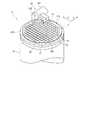
図1の(a)および(b)には、本発明によるウエーハの加工方法によって個々のデバイスに分割される半導体ウエーハの斜視図および要部拡大断面図が示されている。図1の(a)および(b)に示す半導体ウエーハ2は、厚みが例えば140μmのシリコン等の基板20の表面20aに絶縁膜と回路を形成する機能膜が積層された機能層21が形成されており、この機能層21に格子状に形成された複数の分割予定ライン22によって区画された複数の領域にIC、LSI等のデバイス23が形成されている。なお、図示の実施形態においては、機能層21を形成する絶縁膜は、SiO2膜または、SiOF、BSG(SiOB)等の無機物系の膜やポリイミド系、パリレン系等のポリマー膜である有機物系の膜からなる低誘電率絶縁体被膜(Low−k膜)からなっており、厚みが10μmに設定されている。 1A and 1B show a perspective view and an enlarged cross-sectional view of a main part of a semiconductor wafer divided into individual devices by the wafer processing method according to the present invention. A
上述した半導体ウエーハ2を分割予定ラインに沿って分割するウエーハの加工方法について説明する。
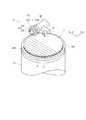
先ず、半導体ウエーハ2を構成する機能層21に形成された分割予定ライン22に沿ってレーザー光線を照射することにより機能層21をアブレーション加工し、機能層21を分割予定ライ22に沿って切断するレーザー加工溝を形成する機能層切断工程を実施する。この機能層切断工程は、図2に示すレーザー加工装置3を用いて実施する。図2に示すレーザー加工装置3は、被加工物を保持するチャックテーブル31と、該チャックテーブル31上に保持された被加工物にレーザー光線を照射するレーザー光線照射手段32と、チャックテーブル31上に保持された被加工物を撮像する撮像手段33を具備している。チャックテーブル31は、被加工物を吸引保持するように構成されており、図示しない加工送り手段によって図2において矢印Xで示す加工送り方向に移動せしめられるとともに、図示しない割り出し送り手段によって図2において矢印Yで示す割り出し送り方向に移動せしめられるようになっている。A wafer processing method for dividing the
First, the
上記レーザー光線照射手段32は、実質上水平に配置された円筒形状のケーシング321を含んでいる。ケーシング321内には図示しないパルスレーザー光線発振器や繰り返し周波数設定手段を備えたパルスレーザー光線発振手段が配設されている。上記ケーシング321の先端部には、パルスレーザー光線発振手段から発振されたパルスレーザー光線を集光するための集光器322が装着されている。なお、レーザー光線照射手段32は、集光器322によって集光されるパルスレーザー光線の集光点位置を調整するための集光点位置調整手段(図示せず)を備えている。 The laser beam irradiation means 32 includes a
上記レーザー光線照射手段32を構成するケーシング321の先端部に装着された撮像手段33は、被加工物を照明する照明手段と、該照明手段によって照明された領域を捕らえる光学系と、該光学系によって捕らえられた像を撮像する撮像素子(CCD)等を備え、撮像した画像信号を図示しない制御手段に送る。 The imaging means 33 attached to the tip of the
上述したレーザー加工装置3を用いて、半導体ウエーハ2を構成する機能層21に形成された分割予定ライン22に沿ってレーザー光線を照射することにより機能層21をアブレーション加工し、機能層21を分割予定ライ22に沿って切断するレーザー加工溝を形成する機能層切断工程について、図2および図3を参照して説明する。
先ず、上述した図2に示すレーザー加工装置3のチャックテーブル31上に半導体ウエーハ2を構成する基板20の裏面20b側を載置する。そして、図示しない吸引手段を作動することにより、半導体ウエーハ2をチャックテーブル31上に保持する(ウエーハ保持工程)。従って、チャックテーブル31に保持された半導体ウエーハ2は、機能層21の表面21aが上側となる。このようにして、半導体ウエーハ2を吸引保持したチャックテーブル31は、図示しない加工送り手段によって撮像手段33の直下に位置付けられる。Using the
First, the
チャックテーブル31が撮像手段33の直下に位置付けられると、撮像手段33および図示しない制御手段によって半導体ウエーハ2のレーザー加工すべき加工領域を検出するアライメント作業を実行する。即ち、撮像手段33および図示しない制御手段は、半導体ウエーハ2の所定方向に形成されている分割予定ライン22と、該分割予定ライン22に沿ってレーザー光線を照射するレーザー光線照射手段32の集光器322との位置合わせを行うためのパターンマッチング等の画像処理を実行し、レーザー光線照射位置のアライメントを遂行する(アライメント工程)。また、半導体ウエーハ2に上記所定方向と直交する方向に形成された分割予定ライン22に対しても、同様にレーザー光線照射位置のアライメントが遂行される。 When the chuck table 31 is positioned immediately below the image pickup means 33, an alignment operation for detecting a processing region to be laser processed of the
上述したアライメント工程を実施したならば、図3の(a)で示すようにチャックテーブル31をレーザー光線を照射するレーザー光線照射手段32の集光器322が位置するレーザー光線照射領域に移動し、所定の分割予定ライン22を集光器322の直下に位置付ける。このとき、図3の(a)で示すように半導体ウエーハ2は、分割予定ライン22の一端(図3の(a)において左端)が集光器322の直下に位置するように位置付けられる。次に、レーザー光線照射手段32の集光器322からパルスレーザー光線LBを照射しつつチャックテーブル31を図3の(a)において矢印X1で示す方向に所定の加工送り速度で移動せしめる。そして、図3の(b)で示すように分割予定ライン22の他端(図3の(b)において右端)が集光器322の直下位置に達したら、パルスレーザー光線の照射を停止するとともにチャックテーブル31の移動を停止する。このレーザー加工溝形成工程においては、パルスレーザー光線の集光点Pを分割予定ライン22の表面付近に合わせる。 When the alignment step described above is performed, the chuck table 31 is moved to the laser beam irradiation region where the
次に、チャックテーブル31を紙面に垂直な方向(割り出し送り方向)に分割予定ライン22の間隔だけ移動する。そして、レーザー光線照射手段32の集光器322からパルスレーザー光線を照射しつつチャックテーブル31を図3の(b)において矢印X2で示す方向に所定の加工送り速度で移動せしめ、図3の(a)に示す位置に達したらパルスレーザー光線の照射を停止するとともにチャックテーブル31の移動を停止する。 Next, the chuck table 31 is moved in the direction perpendicular to the paper surface (index feed direction) by the interval of the division lines 22. Then, while irradiating a pulse laser beam from the
上述した機能層切断工程を実施することにより、図3の(c)に示すように半導体ウエーハ2には機能層21を切断したレーザー加工溝210が形成される。そして、上述した機能層切断工程を半導体ウエーハ2に形成された全ての分割予定ライン22に沿って実施する。 By performing the above-described functional layer cutting step, a
なお、上記機能層切断工程は、例えば以下の加工条件で行われる。
レーザー光線の波長 :355nm
繰り返し周波数 :200kHz
出力 :2W
集光スポット径 :φ6μm
加工送り速度 :500mm/秒In addition, the said functional layer cutting process is performed on the following process conditions, for example.
Laser beam wavelength: 355 nm
Repetition frequency: 200 kHz
Output: 2W
Condensing spot diameter: φ6μm
Processing feed rate: 500 mm / sec
次に、上記機能層切断工程の他の実施形態について、図4を参照して説明する。
図4に示す実施形態は、上記機能層切断工程を実施することによって形成されたレーザー加工溝210が、半導体ウエーハ2を構成する機能層21を分断するとともに基板20の表面20aを僅かに超えて形成された例である。Next, another embodiment of the functional layer cutting step will be described with reference to FIG.
In the embodiment shown in FIG. 4, the
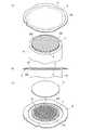
上述した機能層切断工程を実施したならば、半導体ウエーハ2を構成する機能層21の表面に保護部材を貼着する保護部材貼着工程を実施する。即ち、図5の(a)および(b)に示すように半導体ウエーハ2を構成する機能層21の表面21aに、デバイス23を保護するため保護部材4を貼着する(保護部材貼着工程)。なお、保護部材4は、ポリエチレンフィルム等の樹脂シートやガラス基板等の剛性を有するハードプレートを用いることができる。 If the functional layer cutting process mentioned above is implemented, the protective member sticking process which sticks a protective member on the surface of the
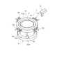
次に、上記保護部材貼着工程が実施された半導体ウエーハ2の保護部材4側をチャックテーブルに保持し、半導体ウエーハ2を構成する基板20の裏面側から分割予定ライン22と対応する領域に切削ブレードを位置付けて機能層21に至らない切削溝を形成する切削溝形成工程を実施する。この切削溝形成工程は、図6に示す切削装置5を用いて実施する。図6に示す切削装置5は、被加工物を保持するチャックテーブル51と、該チャックテーブル51に保持された被加工物を切削する切削手段52と、該チャックテーブル51に保持された被加工物を撮像する撮像手段53を具備している。チャックテーブル51は、被加工物を吸引保持するように構成されており、図示しない加工送り手段によって図6において矢印Xで示す加工送り方向に移動せしめられるとともに、図示しない割り出し送り手段によって矢印Yで示す割り出し送り方向に移動せしめられるようになっている。 Next, the
上記切削手段52は、実質上水平に配置されたスピンドルハウジング521と、該スピンドルハウジング521に回転自在に支持された回転スピンドル522と、該回転スピンドル522の先端部に装着された切削ブレード523を含んでおり、回転スピンドル522がスピンドルハウジング521内に配設された図示しないサーボモータによって矢印523aで示す方向に回転せしめられるようになっている。切削ブレード523は、アルミニウムによって形成された円盤状の基台524と、該基台524の側面外周部に装着された環状の切れ刃525とからなっている。環状の切れ刃525は、基台524の側面外周部に粒径が3〜4μmのダイヤモンド砥粒をニッケルメッキで固めた電鋳ブレードからなっており、図示の実施形態においては厚みが40μmで外径が52mmに形成されている。 The cutting means 52 includes a
上記撮像手段53は、スピンドルハウジング521の先端部に装着されており、図示の実施形態においては可視光線によって撮像する通常の撮像素子(CCD)の外に、被加工物に赤外線を照射する赤外線照明手段と、該赤外線照明手段によって照射された赤外線を捕らえる光学系と、該光学系によって捕らえられた赤外線に対応した電気信号を出力する撮像素子(赤外線CCD)等で構成されており、撮像した画像信号を図示しない制御手段に送る。 The imaging means 53 is attached to the tip of the
上述した切削装置5を用いて切削溝形成工程を実施するには、図6に示すようにチャックテーブル51上に上記保護部材貼着工程が実施され半導体ウエーハ2に貼着された保護部材4側を載置する。そして、図示しない吸引手段を作動することにより、保護部材4を介して半導体ウエーハ2をチャックテーブル51上に保持する(ウエーハ保持工程)。従って、チャックテーブル51に保持された半導体ウエーハ2は、基板20の裏面20bが上側となる。このようにして、半導体ウエーハ2を吸引保持したチャックテーブル51は、図示しない加工送り手段によって撮像手段53の直下に位置付けられる。 In order to perform the cutting groove forming process using the
チャックテーブル51が撮像手段53の直下に位置付けられると、撮像手段53および図示しない制御手段によって半導体ウエーハ2の切削すべき領域を検出するアライメント工程を実行する。即ち、撮像手段53および図示しない制御手段は、半導体ウエーハ2の所定方向に形成されている分割予定ライン22と対応する領域と、切削ブレード523との位置合わせを行うためのパターンマッチング等の画像処理を実行し、切削ブレード523による切削領域のアライメントを遂行する(アライメント工程)。また、半導体ウエーハ2に上記所定方向と直交する方向に形成された分割予定ライン22と対応する領域に対しても、同様に切削ブレード523による切削位置のアライメントが遂行される。このとき、半導体ウエーハ2の分割予定ライン22が形成されている機能層21の表面21aは下側に位置しているが、撮像手段53が上述したように赤外線照明手段と赤外線を捕らえる光学系および赤外線に対応した電気信号を出力する撮像素子(赤外線CCD)等で構成された撮像手段を備えているので、ウエーハを構成する基板20の裏面20bから透かして分割予定ライン22を撮像することができる。 When the chuck table 51 is positioned immediately below the image pickup means 53, an alignment process for detecting an area to be cut of the
以上のようにしてチャックテーブル51上に保持されている半導体ウエーハ2の分割予定ライン22と対応する領域を検出し、切削領域のアライメントが行われたならば、半導体ウエーハ2を保持したチャックテーブル51を切削領域の切削開始位置に移動する。このとき、図7の(a)で示すように半導体ウエーハ2は切削すべき分割予定ライン22と対応する領域の一端(図7の(a)において左端)が切削ブレード523の直下より所定量右側に位置するように位置付けられる。 When the region corresponding to the
このようにしてチャックテーブル51即ち半導体ウエーハ2が切削加工領域の切削開始位置に位置付けられたならば、切削ブレード523を図7(a)において2点鎖線で示す待機位置から矢印Z1で示すように下方に切り込み送りし、図7の(a)において実線で示すように所定の切り込み送り位置に位置付ける。この切り込み送り位置は、図7の(a)および図7の(c)に示すように切削ブレード523の下端が半導体ウエーハ2を構成する機能層21に至らない位置(例えば、機能層21が積層されている基板20の表面20aから裏面20b側に5〜10μmの位置)に設定されている。 When the chuck table 51, that is, the
次に、切削ブレード523を図7の(a)において矢印523aで示す方向に所定の回転速度で回転せしめ、チャックテーブル51を図7の(a)において矢印X1で示す方向に所定の切削送り速度で移動せしめる。そして、チャックテーブル51が図7の(b)で示すように分割予定ライン22に対応する位置の他端(図7の(b)において右端)が切削ブレード523の直下より所定量左側に位置するまで達したら、チャックテーブル51の移動を停止する。このようにチャックテーブル51を切削送りすることにより、図7の(d)で示すように半導体ウエーハ2の基板20には裏面20bから表面20a側に一部201を残して切削溝220が形成される(切削溝形成工程)。即ち、この実施形態においては、切削溝220は機能層21を切断したレーザー加工溝210の底に達していない。 Next, the
次に、切削ブレード523を図7の(b)において矢印Z2で示すように上昇させて2点鎖線で示す待機位置に位置付け、チャックテーブル51を図7の(b)において矢印X2で示す方向に移動して、図7の(a)に示す位置に戻す。そして、チャックテーブル51を紙面に垂直な方向(割り出し送り方向)に分割予定ライン22の間隔に相当する量だけ割り出し送りし、次に切削すべき分割予定ライン22に対応する領域を切削ブレード523と対応する位置に位置付ける。このようにして、次に切削すべき分割予定ライン22に対応する領域を切削ブレード523と対応する位置に位置付けたならば、上述した切削溝形成工程を実施する。 Next, the
なお、上記切削溝形成工程は、例えば以下の加工条件で行われる。
切削ブレード :外径52mm、厚さ40μm
切削ブレードの回転速度:30000rpm
切削送り速度 :50mm/秒In addition, the said cutting groove formation process is performed on the following process conditions, for example.
Cutting blade: outer diameter 52mm, thickness 40μm
Cutting blade rotation speed: 30000 rpm
Cutting feed rate: 50 mm / sec
上述した切削溝形成工程を半導体ウエーハ2に形成された全ての分割予定ライン22に対応する領域に実施する。 The above-described cutting groove forming process is performed on the regions corresponding to all the division lines 22 formed on the
次に、上記切削溝形成工程の他の実施形態について、図8を参照して説明する。
図8に示す実施形態は、上記図4に示すようにレーザー加工溝210が機能層21を切断するとともに基板20の表面20aを僅かに超えて形成された半導体ウエーハ2に対して上記切削溝形成工程を実施した例であり、レーザー加工溝210の底に達する切削溝220が形成される。従って、半導体ウエーハ2は個々のデバイス23に分割される。Next, another embodiment of the cutting groove forming step will be described with reference to FIG.
In the embodiment shown in FIG. 8, the cutting groove is formed on the
次に、切削溝形成工程が実施された半導体ウエーハ2を構成する基板20の裏面20bにダイシングテープを貼着しダイシングテープの外周部を環状のフレームによって支持するとともに、保護部材4を剥離するウエーハ支持工程を実施する。このウエーハ支持工程について、図9を参照して説明する。図9に示すウエーハ支持工程は、上記切削溝形成工程が実施されたチャックテーブル51上において実施する。即ち、図9の(a)および(b)に示すようにウエーハを収容する大きさの開口部61を備えた環状のフレーム6の裏面に開口部61を覆うように外周部が装着されたダイシングテープ60の表面60a(粘着層が設けられ粘着面が形成されている)を切削溝形成工程が実施されたチャックテーブル51に保持されている半導体ウエーハ2を構成する基板20の裏面20bに貼着する。そして、図9の (c)に示すように半導体ウエーハ2を構成する機能層21の表面に貼着されている保護部材4を剥離する。 Next, a wafer in which a dicing tape is attached to the
上述したようにウエーハ支持工程を実施したならば、半導体ウエーハ2を構成する基板20の裏面が貼着されたダイシングテープ60を拡張してデバイス間を広げるテープ拡張工程を実施する。このテープ拡張工程は、図10に示すテープ拡張装置7を用いて実施する。図10に示すテープ拡張装置7は、上記環状のフレーム6を保持するフレーム保持手段71と、該フレーム保持手段71に保持された環状のフレーム6に装着されたダイシングテープ60を拡張するテープ拡張手段72と、ピックアップコレット73を具備している。フレーム保持手段71は、環状のフレーム保持部材711と、該フレーム保持部材711の外周に配設された固定手段としての複数のクランプ712とからなっている。フレーム保持部材711の上面は環状のフレーム6を載置する載置面711aを形成しており、この載置面711a上に環状のフレーム6が載置される。そして、載置面711a上に載置された環状のフレーム6は、クランプ712によってフレーム保持部材711に固定される。このように構成されたフレーム保持手段71は、テープ拡張手段72によって上下方向に進退可能に支持されている。 If the wafer support process is performed as described above, a tape expansion process is performed to expand the dicing
テープ拡張手段72は、上記環状のフレーム保持部材711の内側に配設される拡張ドラム721を具備している。この拡張ドラム721は、環状のフレーム6の内径より小さく該環状のフレーム6に装着されたダイシングテープ60に貼着される半導体ウエーハ2の外径より大きい内径および外径を有している。また、拡張ドラム721は、下端に支持フランジ722を備えている。図示の実施形態におけるテープ拡張手段72は、上記環状のフレーム保持部材711を上下方向に進退可能な支持手段723を具備している。この支持手段723は、上記支持フランジ722上に配設された複数のエアシリンダ723aからなっており、そのピストンロッド723bが上記環状のフレーム保持部材711の下面に連結される。このように複数のエアシリンダ723aからなる支持手段723は、図11の(a)に示すように環状のフレーム保持部材711を載置面711aが拡張ドラム721の上端と略同一高さとなる基準位置と、図11の(b)に示すように拡張ドラム721の上端より所定量下方の拡張位置の間を上下方向に移動せしめる。 The tape expansion means 72 includes an
以上のように構成されたテープ拡張装置7を用いて実施するテープ拡張工程について図11を参照して説明する。即ち、半導体ウエーハ2が貼着されているダイシングテープ60が装着された環状のフレーム6を、図11の(a)に示すようにフレーム保持手段71を構成するフレーム保持部材711の載置面711a上に載置し、クランプ712によってフレーム保持部材711に固定する(フレーム保持工程)。このとき、フレーム保持部材711は図11の(a)に示す基準位置に位置付けられている。次に、テープ拡張手段72を構成する支持手段723としての複数のエアシリンダ723aを作動して、環状のフレーム保持部材711を図11の(b)に示す拡張位置に下降せしめる。従って、フレーム保持部材711の載置面711a上に固定されている環状のフレーム6も下降するため、図11の(b)に示すように環状のフレーム6に装着されたダイシングテープ60は拡張ドラム721の上端縁に接して拡張せしめられる(テープ拡張工程)。この結果、ダイシングテープ60に貼着されている半導体ウエーハ2には放射状に引張力が作用するため、図7の(d)で示すように半導体ウエーハ2の基板20に裏面20bから表面20a側に一部201を残して切削溝220が形成されている場合には、残存した一部201が破断されるとともにデバイス間に間隔Sが形成される。また、図8に示すように半導体ウエーハ2を構成する機能層21を分断するとともに基板20の表面20aを僅かに超えて形成されたレーザー加工溝210の底に達する切削溝220が形成され半導体ウエーハ2が個々のデバイス23に分割されている場合には、個々のデバイス23に分離されるとともにデバイス間に間隔Sが形成される。 The tape expansion process performed using the tape expansion apparatus 7 configured as described above will be described with reference to FIG. That is, the
次に、図11の(c)に示すようにピックアップコレット73を作動してデバイス23を吸着し、ダイシングテープ60から剥離してピックアップし、図示しないトレーまたはダイボンディング工程に搬送する。なお、ピックアップ工程においては、上述したようにダイシングテープ60に貼着されている個々のデバイス23間の隙間Sが広げられているので、隣接するデバイス23と接触することなく容易にピックアップすることができる。 Next, as shown in FIG. 11 (c), the
以上、本発明を図示の実施形態に基づいて説明したが、本発明は実施形態のみに限定されるものではなく、本発明の趣旨の範囲で種々の変形は可能である。上述した実施形態においてはウエーハを構成する機能層の表面に保護部材を貼着する保護部材貼着工程を実施した後に、ウエーハを構成する基板の裏面側から分割予定ラインと対応する領域に切削ブレードを位置付けて機能層に至らない切削溝を形成する切削溝形成工程を実施した例を示したが、保護部材貼着工程を実施した後、切削溝形成工程を実施する前にウエーハを構成する基板の裏面を研削してウエーハを所定の厚みに形成する裏面研削工程を実施してもよい。 Although the present invention has been described based on the illustrated embodiment, the present invention is not limited to the embodiment, and various modifications are possible within the scope of the gist of the present invention. In the embodiment described above, after carrying out the protective member attaching step for attaching the protective member to the surface of the functional layer constituting the wafer, the cutting blade is applied from the back side of the substrate constituting the wafer to the region corresponding to the division line. Although the example which performed the cutting groove formation process which forms the cutting groove which does not reach a functional layer by positioning is shown, the substrate which constitutes a wafer after implementing a protection member pasting process and before performing a cutting groove formation process A back surface grinding process may be performed in which the back surface is ground to form the wafer to a predetermined thickness.
2:半導体ウエーハ
20:基板
21:機能層
22:分割予定ライン
23:デバイス
210:レーザー加工溝
220:切削溝
3:レーザー加工装置
31:レーザー加工装置のチャックテーブル
32:レーザー光線照射手段
322:集光器
4:保護部材
5:切削装置
51:切削装置のチャックテーブル
52:切削手段
523:切削ブレード
6:環状のフレーム
60:ダイシングテープ
7:テープ拡張装置
71:フレーム保持手段
72:テープ拡張手段
73:ピックアップコレット2: Semiconductor wafer 20: Substrate 21: Functional layer 22: Planned division line 23: Device 210: Laser processing groove 220: Cutting groove 3: Laser processing device 31: Chuck table 32 of laser processing device 32: Laser beam irradiation means 322: Condensing Device 4: Protection member 5: Cutting device 51: Chuck table 52 of cutting device: Cutting means 523: Cutting blade 6: Ring frame 60: Dicing tape 7: Tape expansion device 71: Frame holding device 72: Tape expansion device 73: Pickup collet
Claims (3)
Translated fromJapaneseウエーハを構成する機能層に形成された分割予定ラインに沿ってレーザー光線を照射することにより機能層をアブレーション加工し、機能層を分割予定ラインに沿って切断するレーザー加工溝を形成する機能層切断工程と、
該機能層切断工程が実施されたウエーハを構成する機能層の表面に保護部材を貼着する保護部材貼着工程と、
該保護部材貼着工程が実施されたウエーハの該保護部材側をチャックテーブルに保持し、ウエーハを構成する基板の裏面側から分割予定ラインと対応する領域に切削ブレードを位置付けて機能層に至らない切削溝を形成する切削溝形成工程と、
該切削溝形成工程が実施されたウエーハを構成する基板の裏面にダイシングテープを貼着しダイシングテープの外周部を環状のフレームによって支持するとともに、該保護部材を剥離するウエーハ支持工程と、
該ウエーハ支持工程が実施されたウエーハを構成する基板の裏面が貼着されたダイシングテープを拡張してデバイス間を広げるテープ拡張工程と、を含む、
ことを特徴とするウエーハの加工方法。A wafer processing method in which a wafer in which devices are formed in a plurality of regions partitioned by a plurality of planned division lines formed in a lattice pattern on a functional layer stacked on the surface of the substrate is divided along the planned division lines. There,
Functional layer cutting step of forming a laser processing groove for ablating the functional layer by irradiating a laser beam along the planned division line formed on the functional layer constituting the wafer and cutting the functional layer along the planned division line When,
A protective member adhering step for adhering a protective member to the surface of the functional layer constituting the wafer on which the functional layer cutting step has been performed;
The protective member side of the wafer subjected to the protective member attaching step is held on the chuck table, and the cutting blade is positioned in the region corresponding to the division planned line from the back surface side of the substrate constituting the wafer so as not to reach the functional layer. A cutting groove forming step for forming a cutting groove;
A wafer support step of attaching a dicing tape to the back surface of the substrate constituting the wafer on which the cutting groove forming step has been performed, supporting the outer peripheral portion of the dicing tape with an annular frame, and peeling the protective member;
A tape expansion step of expanding a dicing tape to which a back surface of a substrate constituting the wafer on which the wafer support step has been performed is bonded to expand between devices,
A method for processing a wafer.
Priority Applications (4)
| Application Number | Priority Date | Filing Date | Title |
|---|---|---|---|
| JP2013268612AJP6189208B2 (en) | 2013-12-26 | 2013-12-26 | Wafer processing method |
| TW103138364ATWI621212B (en) | 2013-12-26 | 2014-11-05 | Wafer processing method |
| US14/572,917US9209085B2 (en) | 2013-12-26 | 2014-12-17 | Wafer processing method |
| CN201410827307.9ACN104752346B (en) | 2013-12-26 | 2014-12-25 | wafer processing method |
Applications Claiming Priority (1)
| Application Number | Priority Date | Filing Date | Title |
|---|---|---|---|
| JP2013268612AJP6189208B2 (en) | 2013-12-26 | 2013-12-26 | Wafer processing method |
Publications (2)
| Publication Number | Publication Date |
|---|---|
| JP2015126054A JP2015126054A (en) | 2015-07-06 |
| JP6189208B2true JP6189208B2 (en) | 2017-08-30 |
Family
ID=53482667
Family Applications (1)
| Application Number | Title | Priority Date | Filing Date |
|---|---|---|---|
| JP2013268612AActiveJP6189208B2 (en) | 2013-12-26 | 2013-12-26 | Wafer processing method |
Country Status (4)
| Country | Link |
|---|---|
| US (1) | US9209085B2 (en) |
| JP (1) | JP6189208B2 (en) |
| CN (1) | CN104752346B (en) |
| TW (1) | TWI621212B (en) |
Families Citing this family (13)
| Publication number | Priority date | Publication date | Assignee | Title |
|---|---|---|---|---|
| JP6325279B2 (en)* | 2014-02-21 | 2018-05-16 | 株式会社ディスコ | Wafer processing method |
| CN105364320B (en)* | 2014-08-28 | 2017-05-31 | 深圳富泰宏精密工业有限公司 | Distortion-free cutting method and cutting member |
| JP2017038030A (en)* | 2015-08-14 | 2017-02-16 | 株式会社ディスコ | Wafer processing method and electronic device |
| JP2018074083A (en)* | 2016-11-02 | 2018-05-10 | 株式会社ディスコ | Processing method of wafer |
| JP2018125479A (en)* | 2017-02-03 | 2018-08-09 | 株式会社ディスコ | Wafer processing method |
| JP6808525B2 (en)* | 2017-02-13 | 2021-01-06 | 株式会社ディスコ | Wafer processing method |
| JP6808526B2 (en)* | 2017-02-13 | 2021-01-06 | 株式会社ディスコ | Wafer processing method |
| DE102019124181B4 (en) | 2018-09-28 | 2023-06-15 | Taiwan Semiconductor Manufacturing Co., Ltd. | Singulation method for stacked semiconductor components and stacked semiconductor device |
| US11081392B2 (en)* | 2018-09-28 | 2021-08-03 | Taiwan Semiconductor Manufacturing Co., Ltd. | Dicing method for stacked semiconductor devices |
| US11289378B2 (en)* | 2019-06-13 | 2022-03-29 | Wolfspeed, Inc. | Methods for dicing semiconductor wafers and semiconductor devices made by the methods |
| JP7442938B2 (en)* | 2020-06-05 | 2024-03-05 | 株式会社ディスコ | Wafer processing method and processing equipment |
| JP7611736B2 (en) | 2021-03-09 | 2025-01-10 | 株式会社ディスコ | Laser Processing Method |
| JP2023088588A (en)* | 2021-12-15 | 2023-06-27 | 株式会社ディスコ | Wafer processing method |
Family Cites Families (17)
| Publication number | Priority date | Publication date | Assignee | Title |
|---|---|---|---|---|
| EP0573724B1 (en)* | 1992-06-09 | 1995-09-13 | International Business Machines Corporation | Full-wafer processing of laser diodes with cleaved facets |
| SG67365A1 (en)* | 1995-11-21 | 1999-09-21 | Texas Instruments Inc | Trench scribe line for decreased chip spacing |
| JP2005064231A (en)* | 2003-08-12 | 2005-03-10 | Disco Abrasive Syst Ltd | How to divide a plate |
| TWI226090B (en)* | 2003-09-26 | 2005-01-01 | Advanced Semiconductor Eng | Transparent packaging in wafer level |
| JP2007173475A (en)* | 2005-12-21 | 2007-07-05 | Disco Abrasive Syst Ltd | Wafer division method |
| CN100477162C (en)* | 2006-02-21 | 2009-04-08 | 探微科技股份有限公司 | Method for cutting wafer |
| JP2008235650A (en)* | 2007-03-22 | 2008-10-02 | Disco Abrasive Syst Ltd | Device manufacturing method |
| JP2009088252A (en)* | 2007-09-28 | 2009-04-23 | Sharp Corp | Wafer dicing method and semiconductor chip |
| JP2009272421A (en)* | 2008-05-07 | 2009-11-19 | Disco Abrasive Syst Ltd | Method for manufacturing device |
| JP5495511B2 (en)* | 2008-05-27 | 2014-05-21 | 株式会社ディスコ | Wafer division method |
| JP2010045151A (en)* | 2008-08-12 | 2010-02-25 | Disco Abrasive Syst Ltd | Method of processing optical device wafer |
| JP5495876B2 (en)* | 2010-03-23 | 2014-05-21 | 株式会社ディスコ | Processing method of optical device wafer |
| JP5752933B2 (en)* | 2010-12-17 | 2015-07-22 | 株式会社ディスコ | Processing method of optical device wafer |
| TW201234463A (en)* | 2011-02-01 | 2012-08-16 | Lextar Electronics Corp | Semiconductor device and cutting method thereof |
| JP6078272B2 (en)* | 2012-09-10 | 2017-02-08 | 株式会社ディスコ | Wafer processing method |
| CN103441104B (en)* | 2013-08-29 | 2016-06-22 | 华进半导体封装先导技术研发中心有限公司 | Method for cutting wafer |
| JP6162018B2 (en)* | 2013-10-15 | 2017-07-12 | 株式会社ディスコ | Wafer processing method |
- 2013
- 2013-12-26JPJP2013268612Apatent/JP6189208B2/enactiveActive
- 2014
- 2014-11-05TWTW103138364Apatent/TWI621212B/enactive
- 2014-12-17USUS14/572,917patent/US9209085B2/enactiveActive
- 2014-12-25CNCN201410827307.9Apatent/CN104752346B/enactiveActive
Also Published As
| Publication number | Publication date |
|---|---|
| TW201526161A (en) | 2015-07-01 |
| TWI621212B (en) | 2018-04-11 |
| CN104752346A (en) | 2015-07-01 |
| JP2015126054A (en) | 2015-07-06 |
| CN104752346B (en) | 2019-04-23 |
| US20150187650A1 (en) | 2015-07-02 |
| US9209085B2 (en) | 2015-12-08 |
Similar Documents
| Publication | Publication Date | Title |
|---|---|---|
| JP6189208B2 (en) | Wafer processing method | |
| JP6078376B2 (en) | Wafer processing method | |
| JP6305853B2 (en) | Wafer processing method | |
| JP6178077B2 (en) | Wafer processing method | |
| US9779993B2 (en) | Wafer processing method including attaching a protective tape to a front side of a functional layer to prevent debris adhesion | |
| JP6262006B2 (en) | Wafer processing method and processing apparatus | |
| JP6162018B2 (en) | Wafer processing method | |
| US9698301B2 (en) | Wafer processing method | |
| JP5992731B2 (en) | Wafer processing method | |
| JP6246534B2 (en) | Wafer processing method | |
| KR20110106791A (en) | Processing method of optical device wafer | |
| KR20180050225A (en) | Method for processing wafer | |
| JP2013008831A (en) | Processing method of wafer | |
| JP2017103406A (en) | Wafer processing method | |
| US9455149B2 (en) | Plate-like object processing method | |
| JP6257365B2 (en) | Wafer processing method | |
| JP2016086089A (en) | Wafer processing method | |
| JP6305867B2 (en) | Wafer processing method | |
| JP2015005648A (en) | Wafer processing method | |
| JP6346067B2 (en) | Wafer processing method | |
| JP2015005558A (en) | Wafer processing method |
Legal Events
| Date | Code | Title | Description |
|---|---|---|---|
| A621 | Written request for application examination | Free format text:JAPANESE INTERMEDIATE CODE: A621 Effective date:20161017 | |
| A977 | Report on retrieval | Free format text:JAPANESE INTERMEDIATE CODE: A971007 Effective date:20170615 | |
| TRDD | Decision of grant or rejection written | ||
| A01 | Written decision to grant a patent or to grant a registration (utility model) | Free format text:JAPANESE INTERMEDIATE CODE: A01 Effective date:20170711 | |
| A61 | First payment of annual fees (during grant procedure) | Free format text:JAPANESE INTERMEDIATE CODE: A61 Effective date:20170802 | |
| R150 | Certificate of patent or registration of utility model | Ref document number:6189208 Country of ref document:JP Free format text:JAPANESE INTERMEDIATE CODE: R150 | |
| R250 | Receipt of annual fees | Free format text:JAPANESE INTERMEDIATE CODE: R250 | |
| R250 | Receipt of annual fees | Free format text:JAPANESE INTERMEDIATE CODE: R250 | |
| R250 | Receipt of annual fees | Free format text:JAPANESE INTERMEDIATE CODE: R250 | |
| R250 | Receipt of annual fees | Free format text:JAPANESE INTERMEDIATE CODE: R250 | |
| R250 | Receipt of annual fees | Free format text:JAPANESE INTERMEDIATE CODE: R250 | |
| R250 | Receipt of annual fees | Free format text:JAPANESE INTERMEDIATE CODE: R250 |