JP6181698B2 - Liquid crystal display cell - Google Patents
Liquid crystal display cellDownload PDFInfo
- Publication number
- JP6181698B2 JP6181698B2JP2015081713AJP2015081713AJP6181698B2JP 6181698 B2JP6181698 B2JP 6181698B2JP 2015081713 AJP2015081713 AJP 2015081713AJP 2015081713 AJP2015081713 AJP 2015081713AJP 6181698 B2JP6181698 B2JP 6181698B2
- Authority
- JP
- Japan
- Prior art keywords
- metal
- conductive
- nanowires
- item
- transparent conductor
- Prior art date
- Legal status (The legal status is an assumption and is not a legal conclusion. Google has not performed a legal analysis and makes no representation as to the accuracy of the status listed.)
- Active
Links
Images


Classifications
- H—ELECTRICITY
- H05—ELECTRIC TECHNIQUES NOT OTHERWISE PROVIDED FOR
- H05K—PRINTED CIRCUITS; CASINGS OR CONSTRUCTIONAL DETAILS OF ELECTRIC APPARATUS; MANUFACTURE OF ASSEMBLAGES OF ELECTRICAL COMPONENTS
- H05K3/00—Apparatus or processes for manufacturing printed circuits
- H05K3/22—Secondary treatment of printed circuits
- H05K3/24—Reinforcing the conductive pattern
- H05K3/245—Reinforcing conductive patterns made by printing techniques or by other techniques for applying conductive pastes, inks or powders; Reinforcing other conductive patterns by such techniques
- H—ELECTRICITY
- H01—ELECTRIC ELEMENTS
- H01B—CABLES; CONDUCTORS; INSULATORS; SELECTION OF MATERIALS FOR THEIR CONDUCTIVE, INSULATING OR DIELECTRIC PROPERTIES
- H01B5/00—Non-insulated conductors or conductive bodies characterised by their form
- B—PERFORMING OPERATIONS; TRANSPORTING
- B82—NANOTECHNOLOGY
- B82Y—SPECIFIC USES OR APPLICATIONS OF NANOSTRUCTURES; MEASUREMENT OR ANALYSIS OF NANOSTRUCTURES; MANUFACTURE OR TREATMENT OF NANOSTRUCTURES
- B82Y10/00—Nanotechnology for information processing, storage or transmission, e.g. quantum computing or single electron logic
- B—PERFORMING OPERATIONS; TRANSPORTING
- B82—NANOTECHNOLOGY
- B82Y—SPECIFIC USES OR APPLICATIONS OF NANOSTRUCTURES; MEASUREMENT OR ANALYSIS OF NANOSTRUCTURES; MANUFACTURE OR TREATMENT OF NANOSTRUCTURES
- B82Y30/00—Nanotechnology for materials or surface science, e.g. nanocomposites
- G—PHYSICS
- G02—OPTICS
- G02F—OPTICAL DEVICES OR ARRANGEMENTS FOR THE CONTROL OF LIGHT BY MODIFICATION OF THE OPTICAL PROPERTIES OF THE MEDIA OF THE ELEMENTS INVOLVED THEREIN; NON-LINEAR OPTICS; FREQUENCY-CHANGING OF LIGHT; OPTICAL LOGIC ELEMENTS; OPTICAL ANALOGUE/DIGITAL CONVERTERS
- G02F1/00—Devices or arrangements for the control of the intensity, colour, phase, polarisation or direction of light arriving from an independent light source, e.g. switching, gating or modulating; Non-linear optics
- H—ELECTRICITY
- H05—ELECTRIC TECHNIQUES NOT OTHERWISE PROVIDED FOR
- H05K—PRINTED CIRCUITS; CASINGS OR CONSTRUCTIONAL DETAILS OF ELECTRIC APPARATUS; MANUFACTURE OF ASSEMBLAGES OF ELECTRICAL COMPONENTS
- H05K3/00—Apparatus or processes for manufacturing printed circuits
- H05K3/22—Secondary treatment of printed circuits
- H05K3/24—Reinforcing the conductive pattern
- H05K3/245—Reinforcing conductive patterns made by printing techniques or by other techniques for applying conductive pastes, inks or powders; Reinforcing other conductive patterns by such techniques
- H05K3/247—Finish coating of conductors by using conductive pastes, inks or powders
- H05K3/249—Finish coating of conductors by using conductive pastes, inks or powders comprising carbon particles as main constituent
- H—ELECTRICITY
- H10—SEMICONDUCTOR DEVICES; ELECTRIC SOLID-STATE DEVICES NOT OTHERWISE PROVIDED FOR
- H10D—INORGANIC ELECTRIC SEMICONDUCTOR DEVICES
- H10D64/00—Electrodes of devices having potential barriers
- H10D64/20—Electrodes characterised by their shapes, relative sizes or dispositions
- H10D64/205—Nanosized electrodes, e.g. nanowire electrodes
- H—ELECTRICITY
- H10—SEMICONDUCTOR DEVICES; ELECTRIC SOLID-STATE DEVICES NOT OTHERWISE PROVIDED FOR
- H10F—INORGANIC SEMICONDUCTOR DEVICES SENSITIVE TO INFRARED RADIATION, LIGHT, ELECTROMAGNETIC RADIATION OF SHORTER WAVELENGTH OR CORPUSCULAR RADIATION
- H10F71/00—Manufacture or treatment of devices covered by this subclass
- H10F71/138—Manufacture of transparent electrodes, e.g. transparent conductive oxides [TCO] or indium tin oxide [ITO] electrodes
- G—PHYSICS
- G02—OPTICS
- G02F—OPTICAL DEVICES OR ARRANGEMENTS FOR THE CONTROL OF LIGHT BY MODIFICATION OF THE OPTICAL PROPERTIES OF THE MEDIA OF THE ELEMENTS INVOLVED THEREIN; NON-LINEAR OPTICS; FREQUENCY-CHANGING OF LIGHT; OPTICAL LOGIC ELEMENTS; OPTICAL ANALOGUE/DIGITAL CONVERTERS
- G02F1/00—Devices or arrangements for the control of the intensity, colour, phase, polarisation or direction of light arriving from an independent light source, e.g. switching, gating or modulating; Non-linear optics
- G02F1/01—Devices or arrangements for the control of the intensity, colour, phase, polarisation or direction of light arriving from an independent light source, e.g. switching, gating or modulating; Non-linear optics for the control of the intensity, phase, polarisation or colour
- G02F1/13—Devices or arrangements for the control of the intensity, colour, phase, polarisation or direction of light arriving from an independent light source, e.g. switching, gating or modulating; Non-linear optics for the control of the intensity, phase, polarisation or colour based on liquid crystals, e.g. single liquid crystal display cells
- G02F1/133—Constructional arrangements; Operation of liquid crystal cells; Circuit arrangements
- G02F1/1333—Constructional arrangements; Manufacturing methods
- G02F1/1343—Electrodes
- G02F1/13439—Electrodes characterised by their electrical, optical, physical properties; materials therefor; method of making
- H—ELECTRICITY
- H05—ELECTRIC TECHNIQUES NOT OTHERWISE PROVIDED FOR
- H05K—PRINTED CIRCUITS; CASINGS OR CONSTRUCTIONAL DETAILS OF ELECTRIC APPARATUS; MANUFACTURE OF ASSEMBLAGES OF ELECTRICAL COMPONENTS
- H05K1/00—Printed circuits
- H05K1/02—Details
- H05K1/09—Use of materials for the conductive, e.g. metallic pattern
- H05K1/092—Dispersed materials, e.g. conductive pastes or inks
- H05K1/097—Inks comprising nanoparticles and specially adapted for being sintered at low temperature
- H—ELECTRICITY
- H05—ELECTRIC TECHNIQUES NOT OTHERWISE PROVIDED FOR
- H05K—PRINTED CIRCUITS; CASINGS OR CONSTRUCTIONAL DETAILS OF ELECTRIC APPARATUS; MANUFACTURE OF ASSEMBLAGES OF ELECTRICAL COMPONENTS
- H05K2201/00—Indexing scheme relating to printed circuits covered by H05K1/00
- H05K2201/01—Dielectrics
- H05K2201/0104—Properties and characteristics in general
- H05K2201/0108—Transparent
- H—ELECTRICITY
- H05—ELECTRIC TECHNIQUES NOT OTHERWISE PROVIDED FOR
- H05K—PRINTED CIRCUITS; CASINGS OR CONSTRUCTIONAL DETAILS OF ELECTRIC APPARATUS; MANUFACTURE OF ASSEMBLAGES OF ELECTRICAL COMPONENTS
- H05K2201/00—Indexing scheme relating to printed circuits covered by H05K1/00
- H05K2201/02—Fillers; Particles; Fibers; Reinforcement materials
- H05K2201/0203—Fillers and particles
- H05K2201/0242—Shape of an individual particle
- H05K2201/026—Nanotubes or nanowires
- H—ELECTRICITY
- H10—SEMICONDUCTOR DEVICES; ELECTRIC SOLID-STATE DEVICES NOT OTHERWISE PROVIDED FOR
- H10D—INORGANIC ELECTRIC SEMICONDUCTOR DEVICES
- H10D62/00—Semiconductor bodies, or regions thereof, of devices having potential barriers
- H10D62/10—Shapes, relative sizes or dispositions of the regions of the semiconductor bodies; Shapes of the semiconductor bodies
- H10D62/117—Shapes of semiconductor bodies
- H10D62/118—Nanostructure semiconductor bodies
- H10D62/119—Nanowire, nanosheet or nanotube semiconductor bodies
- H—ELECTRICITY
- H10—SEMICONDUCTOR DEVICES; ELECTRIC SOLID-STATE DEVICES NOT OTHERWISE PROVIDED FOR
- H10K—ORGANIC ELECTRIC SOLID-STATE DEVICES
- H10K50/00—Organic light-emitting devices
- H10K50/80—Constructional details
- H10K50/805—Electrodes
- H10K50/81—Anodes
- H—ELECTRICITY
- H10—SEMICONDUCTOR DEVICES; ELECTRIC SOLID-STATE DEVICES NOT OTHERWISE PROVIDED FOR
- H10K—ORGANIC ELECTRIC SOLID-STATE DEVICES
- H10K85/00—Organic materials used in the body or electrodes of devices covered by this subclass
- H10K85/20—Carbon compounds, e.g. carbon nanotubes or fullerenes
- H10K85/221—Carbon nanotubes
- Y—GENERAL TAGGING OF NEW TECHNOLOGICAL DEVELOPMENTS; GENERAL TAGGING OF CROSS-SECTIONAL TECHNOLOGIES SPANNING OVER SEVERAL SECTIONS OF THE IPC; TECHNICAL SUBJECTS COVERED BY FORMER USPC CROSS-REFERENCE ART COLLECTIONS [XRACs] AND DIGESTS
- Y02—TECHNOLOGIES OR APPLICATIONS FOR MITIGATION OR ADAPTATION AGAINST CLIMATE CHANGE
- Y02E—REDUCTION OF GREENHOUSE GAS [GHG] EMISSIONS, RELATED TO ENERGY GENERATION, TRANSMISSION OR DISTRIBUTION
- Y02E10/00—Energy generation through renewable energy sources
- Y02E10/50—Photovoltaic [PV] energy
Landscapes
- Engineering & Computer Science (AREA)
- Chemical & Material Sciences (AREA)
- Nanotechnology (AREA)
- Physics & Mathematics (AREA)
- Crystallography & Structural Chemistry (AREA)
- Microelectronics & Electronic Packaging (AREA)
- Manufacturing & Machinery (AREA)
- General Physics & Mathematics (AREA)
- Materials Engineering (AREA)
- Theoretical Computer Science (AREA)
- Composite Materials (AREA)
- Condensed Matter Physics & Semiconductors (AREA)
- Mathematical Physics (AREA)
- Nonlinear Science (AREA)
- Optics & Photonics (AREA)
- Non-Insulated Conductors (AREA)
- Manufacturing Of Electric Cables (AREA)
- Liquid Crystal (AREA)
- Laminated Bodies (AREA)
- Separation Of Solids By Using Liquids Or Pneumatic Power (AREA)
Description
Translated fromJapanese (発明の分野)
本開示は、導電性ナノ構造に基づく複合透明導電体と、それを形成するための方法とに関する。(Field of Invention)
The present disclosure relates to composite transparent conductors based on conductive nanostructures and methods for forming the same.
透明導電体は、光透過性導電性薄膜を指す。透明導電体は、液晶ディスプレイ、プラズマディスプレイ、タッチパネル、エレクトロルミネセント素子、および薄膜太陽電池等のフラットパネルディスプレイにおける透明電極として、帯電防止層として、ならびに電磁波遮蔽層として広く使用されている。 The transparent conductor refers to a light transmissive conductive thin film. Transparent conductors are widely used as transparent electrodes, antistatic layers, and electromagnetic wave shielding layers in flat panel displays such as liquid crystal displays, plasma displays, touch panels, electroluminescent devices, and thin film solar cells.
従来の透明導電体には、インジウムスズ酸化物(ITO)等の真空蒸着金属酸化物が含まれる。しかしながら、金属酸化物膜は、高導電率を達成するために、真空チャンバ、上昇蒸着温度、および/または高い焼きなまし温度を必要とすることから、加工に費用が掛かる。また、金属酸化物膜は、屈曲等の微量の物理的応力を受ける場合であっても、脆弱で破損し易い。 Conventional transparent conductors include vacuum deposited metal oxides such as indium tin oxide (ITO). However, metal oxide films are expensive to process because they require a vacuum chamber, elevated deposition temperature, and / or high annealing temperature to achieve high conductivity. Further, the metal oxide film is fragile and easily damaged even when subjected to a small amount of physical stress such as bending.
また、導電性高分子も、光透過性電導体として使用されてきた。しかしながら、導電性高分子は、概して、金属化学物皮膜よりも低い導電率値および高い光吸収性を有し(特に可視波長で)、化学的および長期的安定性の不足を被る。 Conductive polymers have also been used as light transmissive conductors. However, conductive polymers generally have lower conductivity values and higher light absorption than metal chemical films (especially at visible wavelengths) and suffer from a lack of chemical and long-term stability.
導電性ナノ構造は、そのサブミクロン寸法により光透過性導電性膜を形成することが可能である。同時係属および共有の特許文献1、特許文献2、および特許文献3は、金属ナノワイヤ等の網状異方性導電性ナノ構造によって形成される透明導電体について説明している。ITO膜と同様に、ナノ構造ベースの透明導電体は、フラットパネルディスプレイおよびタッチスクリーン等のエレクトロクロミックディスプレイにおける薄膜トランジスタに連結可能である電極として特に有用である。加えて、ナノ構造ベースの透明導電体は、色フィルタおよび偏光子における塗膜として、偏光子として、およびその他のものとしても適切である。上記同時係属出願は、参照によりその全体が本明細書に組み込まれる。 The conductive nanostructure can form a light-transmitting conductive film due to its submicron size. Co-pending and sharing
高品質のディスプレイシステムに対する需要増加を満たすために、費用効率が高く、かつ高性能であるナノ構造ベースの透明導電体を提供する必要性が存在する。 In order to meet the growing demand for high quality display systems, there is a need to provide a nanostructure based transparent conductor that is cost effective and high performance.
複合透明導電体およびその用途について説明する。 The composite transparent conductor and its use will be described.
一実施形態は、複数の金属ナノワイヤまたは複数の金属ナノチューブを含む一次導電性媒体と、一次導電性媒体に連結される二次導電性媒体であって、第2の種類のナノ構造または連続導電性薄膜を含む二次導電性媒体とを備える複合透明導電体について説明する。 One embodiment is a primary conductive medium comprising a plurality of metal nanowires or a plurality of metal nanotubes, and a secondary conductive medium coupled to the primary conductive medium, the second type of nanostructure or continuous conductivity A composite transparent conductor including a secondary conductive medium including a thin film will be described.
別の実施形態は、複数の金属ナノワイヤまたは複数の金属ナノチューブを含む一次導電性媒体と、一次導電性媒体に連結される二次導電性媒体であって、連続導電性薄膜である二次導電性媒体とを備える機器について説明する。 Another embodiment is a primary conductive medium comprising a plurality of metal nanowires or a plurality of metal nanotubes, and a secondary conductive medium coupled to the primary conductive medium, the secondary conductive medium being a continuous conductive thin film A device including a medium will be described.
さらなる実施形態は、第1の電極と、第2の電極であって、第1の電極および前記第2の電極の間の垂直距離はセルギャップを規定する第2の電極とを備え、第1の電極は、一次導電性媒体および二次導電性媒体を含む複合透明導電体であり、一次導電性媒体は、セルギャップと類似のメッシュサイズを有する金属ナノワイヤまたは金属ナノチューブを含み、二次導電性媒体は、セルギャップの約1/5から1/100までのメッシュサイズを有する連続導電性薄膜またはナノ構造の導電性網である、液晶ディスプレイセルについて説明する。 A further embodiment comprises a first electrode and a second electrode, wherein a vertical distance between the first electrode and the second electrode defines a cell gap, and the first electrode The electrode is a composite transparent conductor including a primary conductive medium and a secondary conductive medium, and the primary conductive medium includes a metal nanowire or a metal nanotube having a mesh size similar to a cell gap, and has a secondary conductivity. A liquid crystal display cell is described in which the medium is a continuous conductive thin film or nanostructured conductive network having a mesh size of about 1/5 to 1/100 of the cell gap.
図面において、同一の参照番号は、類似の要素または作用を示す。図面における要素のサイズおよび相対位置は、必ずしも一定の縮尺で描かれてはいない。例えば、種々の要素の形状および角度は一定の縮尺で描かれず、これらの要素のいくつかは、図面の視認性を改善するために、任意により拡大および配置されている。さらに、描かれる要素の特定の形状は、特定の要素の実際の形状に関するいかなる情報も伝えることを意図せず、単に、図面を認識し易いように選択されただけである。
概して、複合透明導電体は、少なくとも2つの種類の透明導電性媒体から形成される導電性膜である。より具体的には、複合透明導電体は、一次導電性媒体としての金属異方性ナノ構造(本明細書で上述した)と、一次導電性媒体に連結される二次導電性媒体とを含む。典型的には、二次導電性媒体は、第2の種類の導電性ナノ構造の導電性網、または導電性ポリマーもしくは金属酸化物から形成される連続導電性薄膜である。 In general, a composite transparent conductor is a conductive film formed from at least two types of transparent conductive media. More specifically, the composite transparent conductor includes a metal anisotropic nanostructure (described above in this specification) as a primary conductive medium and a secondary conductive medium coupled to the primary conductive medium. . Typically, the secondary conductive medium is a conductive network of a second type of conductive nanostructure, or a continuous conductive thin film formed from a conductive polymer or metal oxide.
複合透明導電体の電気的特性および光学的特性は、構成導電性媒体の幾何学的形状、導電率、光学的特性、分布、および荷重レベル等の要因によって判断される。 The electrical and optical properties of the composite transparent conductor are determined by factors such as the geometric shape, conductivity, optical properties, distribution, and load level of the constituent conductive media.
特定の実施形態では、複合透明導電体は、個別の導電性膜の層状構造である。他の実施形態では、複合透明導電体は、2つ以上の種類の導電性媒体(例えば、2つ以上の種類の導電性ナノ構造)が完全に統合される凝集構造である。構造構成にかかわらず、複合透明導電体は、構成導電性媒体の単なる相加的効果を上回る特性を、このような構成導電性媒体の賢明な選択によって呈することが可能である。 In certain embodiments, the composite transparent conductor is a layered structure of discrete conductive films. In other embodiments, the composite transparent conductor is an aggregated structure in which two or more types of conductive media (eg, two or more types of conductive nanostructures) are fully integrated. Regardless of the structural configuration, the composite transparent conductor can exhibit properties beyond the mere additive effects of the constituent conductive media by judicious selection of such constituent conductive media.
(導電性ナノ構造)
特定の実施形態では、複合透明導電体は、少なくとも2つの種類のナノ構造を備え、そのうちの1つは、金属異方性ナノ構造を対象とする。本明細書において使用する際、「ナノ構造」または「導電性ナノ構造」は、概して、ナノサイズの構造を指し、その少なくとも1つの寸法は、500nm未満、より好ましくは、250nm、100nm、50nm、または25nm未満である。(Conductive nanostructure)
In certain embodiments, the composite transparent conductor comprises at least two types of nanostructures, one of which is directed to a metal anisotropic nanostructure. As used herein, “nanostructure” or “conductive nanostructure” generally refers to a nanosized structure, at least one dimension of which is less than 500 nm, more preferably 250 nm, 100 nm, 50 nm, Or less than 25 nm.
ナノ構造は、任意の形状または幾何学的形状を有することが可能である。特定の実施形態では、ナノ構造は、等方的形状(すなわち、アスペクト比=1)である。典型的な等方性ナノ構造には、ナノ粒子が含まれる。好適な実施形態では、ナノ構造は、等方的形状(すなわち、アスペクト比≠1)である。本明細書において使用する際、アスペクト比は、ナノ構造の長さおよび幅(または直径)の比率を指す。典型的には、異方性ナノ構造は、その長さに沿って長手方向軸を有する。例示的な異方性ナノ構造には、本明細書に定義するように、ナノワイヤおよびナノチューブが含まれる。 Nanostructures can have any shape or geometric shape. In certain embodiments, the nanostructure is isotropic (ie, aspect ratio = 1). Typical isotropic nanostructures include nanoparticles. In a preferred embodiment, the nanostructure is isotropic (ie, aspect ratio ≠ 1). As used herein, aspect ratio refers to the ratio of length and width (or diameter) of nanostructures. Typically, anisotropic nanostructures have a longitudinal axis along their length. Exemplary anisotropic nanostructures include nanowires and nanotubes, as defined herein.
ナノ構造は、中実または中空であることが可能である。中実ナノ構造には、例えば、ナノ粒子およびナノワイヤが含まれる。「ナノワイヤ」は、本明細書に定義するように、中実異方性ナノ構造を指す。典型的には、各ナノワイヤは、10を上回る、好ましくは50を上回る、より好ましくは100を上回るアスペクト比(長さ:直径)を有する。典型的には、ナノワイヤは、500nmを上回る、または1μmを上回る、または10μmを上回る長さを有する。 Nanostructures can be solid or hollow. Solid nanostructures include, for example, nanoparticles and nanowires. “Nanowire” refers to a solid anisotropic nanostructure, as defined herein. Typically, each nanowire has an aspect ratio (length: diameter) greater than 10, preferably greater than 50, more preferably greater than 100. Typically, nanowires have a length greater than 500 nm, or greater than 1 μm, or greater than 10 μm.
中空ナノ構造には、例えば、ナノチューブが含まれる。「ナノチューブ」は、本明細書に定義するように、中空異方性ナノ構造を指す。典型的には、ナノチューブは、10を上回る、好ましくは50を上回る、より好ましくは100を上回るアスペクト比(長さ:直径)を有する。典型的には、ナノワイヤは、500nmを上回る、または1μmを上回る、または10μmを上回る長さを有する。 Hollow nanostructures include, for example, nanotubes. “Nanotube” refers to a hollow anisotropic nanostructure, as defined herein. Typically, the nanotubes have an aspect ratio (length: diameter) of greater than 10, preferably greater than 50, more preferably greater than 100. Typically, nanowires have a length greater than 500 nm, or greater than 1 μm, or greater than 10 μm.
ナノ構造は、任意の導電性材料から形成可能である。最も典型的には、導電性材料は、金属である。金属材料は、元素金属(例えば、遷移金属)または金属化合物(例えば、金属酸化物)であることが可能である。また、金属材料は、2つ以上の種類の金属を含む金属合金または2種の金属からなる材料であることが可能である。適切な金属には、銀、金、胴、ニッケル、金めっき銀、白金、およびパラジウムが含まれるが、これらに限定されない。また、導電性材料は、炭素または黒鉛(炭素の同素体)等の非金属であることも可能である。 Nanostructures can be formed from any conductive material. Most typically, the conductive material is a metal. The metal material can be an elemental metal (eg, a transition metal) or a metal compound (eg, a metal oxide). The metal material can be a metal alloy containing two or more kinds of metals or a material made of two kinds of metals. Suitable metals include, but are not limited to, silver, gold, barrel, nickel, gold plated silver, platinum, and palladium. The conductive material can also be a nonmetal such as carbon or graphite (carbon allotrope).
上述のように、金属異方性ナノ構造は、複合透明導電体における一次導電性媒体として使用される。好適な種類の異方性金属ナノ構造には、金属ナノワイヤが含まれる。金属ナノワイヤは、金属、金属合金、めっき金属、または金属酸化物から形成されるナノワイヤである。適切な金属ナノワイヤには、銀ナノワイヤ、金ナノワイヤ、銅ナノワイヤ、ニッケルナノワイヤ、金めっき銀ナノワイヤ、白金ナノワイヤ、およびパラジウムナノワイヤが含まれるが、これらに限定されない。同時係属および共有の米国出願第11/766,552号、第11/504,822号、第11/871,767号、および第11/871,721号は、金属ナノワイヤ(例えば、銀ナノワイヤ)を調製する方法と、金属ナノワイヤに基づく透明導電体を形成およびパターン化する方法とについて説明しており、その説明は、参照によりその全体が本明細書に組み込まれる。 As described above, the metal anisotropic nanostructure is used as a primary conductive medium in a composite transparent conductor. Suitable types of anisotropic metal nanostructures include metal nanowires. Metal nanowires are nanowires formed from metals, metal alloys, plated metals, or metal oxides. Suitable metal nanowires include, but are not limited to, silver nanowires, gold nanowires, copper nanowires, nickel nanowires, gold plated silver nanowires, platinum nanowires, and palladium nanowires. Co-pending and sharing U.S. Application Nos. 11 / 766,552, 11 / 504,822, 11 / 871,767, and 11 / 871,721 are based on metal nanowires (eg, silver nanowires). It describes a method of preparation and a method of forming and patterning transparent conductors based on metal nanowires, the description of which is incorporated herein by reference in its entirety.
一次導電性媒体に使用される別の好適な種類の異方性金属ナノ構造には、金属ナノチューブが含まれる。2008年2月26日に出願された同時係属および共有の米国特許出願第61/031,643号は、金属ナノチューブ(例えば、金ナノチューブ)を調製する方法と、金属ナノチューブに基づく透明導電体の形成およびパターン化の方法とについて説明しており、その説明は、参照によりその全体が本明細書に組み込まれる。 Another suitable type of anisotropic metal nanostructure used for primary conductive media includes metal nanotubes. Co-pending and co-owned US Patent Application No. 61 / 031,643, filed February 26, 2008, describes a method for preparing metal nanotubes (eg, gold nanotubes) and the formation of transparent conductors based on metal nanotubes. And a patterning method, the description of which is incorporated herein by reference in its entirety.
本明細書においてより詳細に論じるように、ナノワイヤおよびナノチューブ等の金属異方性ナノ構造は、異なる種類の導電性ナノ構造により形成される二次導電性媒体と組み合わせ可能である。二次導電性媒体は、カーボンナノチューブ、一次導電性媒体を形成する金属ナノワイヤ(または、ナノチューブ)とは異なる金属ナノワイヤ(または、ナノチューブ)、導電性ナノ粒子、およびその同等物を含むが、これらに限定されないナノ構造のうちのいずれかであることが可能である。 As discussed in more detail herein, metal anisotropic nanostructures such as nanowires and nanotubes can be combined with secondary conductive media formed by different types of conductive nanostructures. Secondary conductive media include, but are not limited to, carbon nanotubes, metal nanowires (or nanotubes) that are different from the metal nanowires (or nanotubes) that form the primary conductive media, conductive nanoparticles, and the like. It can be any of the non-limiting nanostructures.
特定の具体的な実施形態では、二次導電性媒体を形成する導電性ナノ構造は、カーボンナノチューブである。カーボンナノチューブも、導電性異方性ナノ構造である。より具体的には、「カーボンナノチューブ」は、巻き上げ状グラフェンシートの円筒または管を指す。各グラフェンシートは、sp2混成炭素原子を含む。カーボンナノチューブは、単層構造もしくは多層構造またはその混合のいずれかの形状をとることが可能である。単層カーボンナノチューブ(SWNT)は、単一の巻き上げ状グラフェンシートから形成される。多層カーボンナノチューブ(MWNT)は、相互に入れ子式である2つ以上の同軸上に配置されるSWNTである。SWNTおよびMWNTの両方は、金属特徴および導電性特徴を示すことで知られている。In certain specific embodiments, the conductive nanostructures forming the secondary conductive medium are carbon nanotubes. Carbon nanotubes are also conductive anisotropic nanostructures. More specifically, “carbon nanotubes” refer to a rolled graphene sheet cylinder or tube. Each graphene sheet contains sp2 hybridized carbon atoms. Carbon nanotubes can take the form of either a single-layer structure, a multi-layer structure, or a mixture thereof. Single-walled carbon nanotubes (SWNT) are formed from a single rolled graphene sheet. Multi-walled carbon nanotubes (MWNTs) are two or more coaxially arranged SWNTs that are nested with each other. Both SWNTs and MWNTs are known to exhibit metallic and conductive characteristics.
典型的には、カーボンナノチューブは、高アスペクト比を有する剛性構造である。SWNTおよびMWNTの長さは、通常1μmを十分上回り、直径は、約1nm(SWNTの場合)から約50nm(MWNTの場合)までの範囲である。典型的には、カーボンナノチューブのアスペクト比は、約10−100,000の範囲である。より典型的には、アスペクト比は、約1,000−10,000の範囲である。SWNTは、Sigma−Aldrich(St.Louis,MO)より市販されている。 Typically, carbon nanotubes are rigid structures having a high aspect ratio. The length of SWNT and MWNT is usually well above 1 μm and the diameter ranges from about 1 nm (for SWNT) to about 50 nm (for MWNT). Typically, the aspect ratio of carbon nanotubes is in the range of about 10-100,000. More typically, the aspect ratio is in the range of about 1,000-10,000. SWNT is commercially available from Sigma-Aldrich (St. Louis, MO).
カーボンナノチューブは、任意により、凝集防止のために表面処理され得る。例えば、より良好に水媒体へ分散するように、親水性官能基が表面に組み込まれ得る。表面処理に関する種々の方法については、Peng H.らのSidewall Carboxylic Acid Functionalization of Single−Walled Carbon Nanotubes、J.Am.Chem.Soc.125、15174−15182、2003、およびLiu J.らのFullerene Pipes、Science、280、1253−1256、1998に説明されている。 The carbon nanotubes can optionally be surface treated to prevent aggregation. For example, hydrophilic functional groups can be incorporated on the surface to better disperse in aqueous media. See Peng H. et al. Sidewall Carboxylic Acid Functionalization of Single-Walled Carbon Nanotubes, J. et al. Am. Chem. Soc. 125, 15174-15182, 2003, and Liu J. et al. Fullerene Pipes, Science, 280, 1253-1256, 1998.
さらなる実施形態では、導電性ナノ構造は、銀、金、銅、およびニッケルナノ粒子等の金属ナノ粒子、ならびにインジウムスズ酸化物およびドープ酸化亜鉛ナノ粒子等の金属酸化物ナノ粒子を含む導電性ナノ粒子である。非金属導電性ナノ粒子には、カーボンブラック、グラフェンシート、およびその同等物が含まれる。これらの導電性ナノ粒子は、当技術分野において周知である。 In a further embodiment, the conductive nanostructure comprises conductive nanoparticles comprising metal nanoparticles such as silver, gold, copper, and nickel nanoparticles, and metal oxide nanoparticles such as indium tin oxide and doped zinc oxide nanoparticles. Particles. Non-metallic conductive nanoparticles include carbon black, graphene sheets, and the like. These conductive nanoparticles are well known in the art.
導電性ナノ構造は、連続的な物理的接触により、ならびに一方のナノ構造から別のナノ構造へ移行する電荷により、電気伝導度を達成することが可能である。 Conductive nanostructures can achieve electrical conductivity by continuous physical contact as well as by the charge transferred from one nanostructure to another.
(一次導電性媒体)
金属ナノワイヤまたは金属ナノチューブは、一次導電性媒体を形成する。適切な金属ナノワイヤは、金属、金属合金、めっき金属、または金属酸化物から形成されるナノワイヤである。適切な金属ナノワイヤには、銀ナノワイヤ、金ナノワイヤ、銅ナノワイヤ、ニッケルナノワイヤ、金めっき銀ナノワイヤ、白金ナノワイヤ、およびパラジウムナノワイヤが含まれるが、これらに限定されない。適切な金属ナノチューブには、金ナノチューブおよび同時係属米国仮出願第61/031,643号に説明されるものが含まれる。(Primary conductive medium)
Metal nanowires or metal nanotubes form the primary conductive medium. Suitable metal nanowires are nanowires formed from metals, metal alloys, plated metals, or metal oxides. Suitable metal nanowires include, but are not limited to, silver nanowires, gold nanowires, copper nanowires, nickel nanowires, gold plated silver nanowires, platinum nanowires, and palladium nanowires. Suitable metal nanotubes include gold nanotubes and those described in co-pending US Provisional Application No. 61 / 031,643.
種々の実施形態では、金属ナノワイヤは、約5−100μmの長さを有し、5−100nmの直径(または、断面)を有する。特定の実施形態では、金属ナノワイヤは、約5−30μmの長さを有し、20−80nmの直径を有する。好適な実施形態では、金属ナノワイヤ(例えば、銀ナノワイヤ)は、約20μmの長さを有し、50nmの直径を有する。 In various embodiments, the metal nanowire has a length of about 5-100 μm and a diameter (or cross section) of 5-100 nm. In certain embodiments, the metal nanowires have a length of about 5-30 μm and a diameter of 20-80 nm. In a preferred embodiment, the metal nanowire (eg, silver nanowire) has a length of about 20 μm and a diameter of 50 nm.
適切な金属ナノチューブは、金属ナノワイヤについて説明した寸法と類似の寸法を有する。ナノチューブでは、直径は、ナノチューブの外径を指す。 Suitable metal nanotubes have dimensions similar to those described for metal nanowires. For nanotubes, the diameter refers to the outer diameter of the nanotube.
ナノ構造は、パーコレーション過程によって導電性網を形成する。パーコレーション導電率は、導電性経路が相互接続ナノ構造によって形成される場合に確立可能である。電気的パーコレーション閾値を達成し、かつ導電性になるためには、十分なナノ構造が存在しなければならない。ゆえに、電気的パーコレーション閾値は、ナノ構造の荷重密度または濃度に関連する臨界値であり、臨界値を上回ると長距離導電率が達成可能である。典型的には、荷重密度は、面積当たりのナノ構造の数を指し、「数/μm2」によって表すことが可能である。Nanostructures form a conductive network through a percolation process. Percolation conductivity can be established when the conductive pathway is formed by interconnected nanostructures. Sufficient nanostructures must be present to achieve the electrical percolation threshold and to become conductive. Thus, the electrical percolation threshold is a critical value related to the load density or concentration of the nanostructure, above which a long-range conductivity can be achieved. Typically, load density refers to the number of nanostructures per area and can be represented by “number / μm2 ”.
同時係属米国特許出願第11/504,822号に説明するように、ナノ構造のアスペクト比(長さ:直径)が高くなると、パーコレーション導電率の達成に必要なナノ構造は少なくなる。ナノワイヤ等の異方性ナノ構造では、電気的パーコレーション閾値または荷重密度は、ナノワイヤの長さの2乗に反比例する。参照によりその全体が本明細書に組み込まれる同時係属および共有の出願第11/871,053号は、ナノワイヤのサイズ/形状と、パーコレーション閾値における表面荷重密度との理論的関係ならびに経験的関係について詳述している。 As described in co-pending US patent application Ser. No. 11 / 504,822, the higher the aspect ratio (length: diameter) of the nanostructure, the fewer nanostructures are required to achieve percolation conductivity. In anisotropic nanostructures such as nanowires, the electrical percolation threshold or load density is inversely proportional to the square of the length of the nanowire. Co-pending and sharing application 11 / 871,053, which is hereby incorporated by reference in its entirety, details the theoretical and empirical relationship between nanowire size / shape and surface load density at the percolation threshold. It is stated.
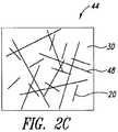
図1は、電気的パーコレーション閾値を上回ってナノワイヤ20により形成される導電性網10を図式的に示す。導電性経路は、ナノワイヤを相互接続すること(例えば、網の一方の端部から他方の端部まで、接続するナノワイヤを通って追跡可能であること)によって形成される。ゆえに、電流は、ナノワイヤ網10を横断して伝導可能である。 FIG. 1 schematically shows a
本明細書において使用する際、「導電性網」または「網」は、電気的パーコレーション閾値を上回る導電性ナノ構造によって形成される相互接続網を指す。典型的には、導電性網の表面抵抗率(または、「シート抵抗」)は、108オーム/スクエア(「Ω/□」とも呼ばれる)未満である。好ましくは、表面抵抗率は、104Ω/□、3,000Ω/□、1,000Ω/□、または100Ω/□未満である。典型的には、金属ナノワイヤにより形成される導電性網の表面抵抗率は、10Ω/□から1000Ω/□、100Ω/□から750Ω/□、50Ω/□から200Ω/□、100Ω/□から500Ω/□、または100Ω/□から250Ω/□、10Ω/□から200Ω/□、10Ω/□から50Ω/□、または1Ω/□から10Ω/□の範囲である。As used herein, “conductive network” or “network” refers to an interconnect network formed by conductive nanostructures that exceed an electrical percolation threshold. Typically, the surface resistivity (or “sheet resistance”) of the conductive network is less than 108 ohms / square (also referred to as “Ω / □”). Preferably, the surface resistivity is less than 104 Ω / □, 3,000 Ω / □, 1,000 Ω / □, or 100 Ω / □. Typically, the surface resistivity of the conductive network formed by the metal nanowires is 10Ω / □ to 1000Ω / □, 100Ω / □ to 750Ω / □, 50Ω / □ to 200Ω / □, 100Ω / □ to 500Ω / □. □, or 100Ω / □ to 250Ω / □, 10Ω / □ to 200Ω / □, 10Ω / □ to 50Ω / □, or 1Ω / □ to 10Ω / □.
また、図1に示すように、網状ナノワイヤは、ワイヤ間空間30を画定する。パーコレーション閾値を上回る際、ワイヤ間空間のサイズ(「メッシュサイズ」とも呼ばれる)は、網の導電率に相関する。典型的には、メッシュサイズが小さいことは、ナノワイヤが密に分散すること意味し、これは高い導電率に相当する。 In addition, as shown in FIG. 1, the reticulated nanowire defines an
また、メッシュサイズは、表面荷重レベルの指標として使用可能である。例えば、所定の長さを有するナノワイヤでは、表面荷重が低くなると、メッシュサイズが大きくなる。メッシュサイズが、特定の閾値を上回ると、ナノワイヤは、離隔し過ぎてパーコレーションが不可能になり、ワイヤ間空間は、効率的に絶縁体になる。図2Aは、ナノワイヤ20が完全な網の形成に不十分な密度にある膜12を示す。ワイヤ間空間30は、絶縁になる。明らかに異なるように、図1の密度に比べてナノワイヤの密度が低いことにより、メッシュサイズは拡大し、ナノワイヤ間の導電率は崩壊している。 The mesh size can also be used as an indicator of the surface load level. For example, in a nanowire having a predetermined length, the mesh size increases as the surface load decreases. When the mesh size exceeds a certain threshold, the nanowires are too far apart to be percolated, and the interwire space is effectively an insulator. FIG. 2A shows the
(充填材としての二次導電性媒体)
複合透明導電体では、金属ナノワイヤが、電気的パーコレーション閾値未満の荷重レベルにある場合であっても、二次導電性媒体の存在下で導電率を達成することが可能である。一次導電性媒体の金属ナノワイヤは、種々の実施形態では、パーコレーションまたは非パーコレーションであるが、第2の導電性媒体の存在は、複合透明導電体において、予想外の特性および相乗特性を提供する。(Secondary conductive medium as filler)
In composite transparent conductors, it is possible to achieve conductivity in the presence of a secondary conductive medium even when the metal nanowires are at a load level below the electrical percolation threshold. The metal nanowires of the primary conductive medium are percolated or non-percolated in various embodiments, but the presence of the second conductive medium provides unexpected and synergistic properties in the composite transparent conductor.
特定の実施形態では、二次導電性媒体は、一次導電性媒体を形成する金属ナノワイヤとは異なる材料、寸法、幾何学的形状、または構造のナノ構造を含む。例えば、二次導電性媒体には、異なる寸法または材料のカーボンナノチューブ、金属ナノチューブ、ナノ粒子、および金属ナノワイヤが含まれ得るが、これらに限定されない。 In certain embodiments, the secondary conductive medium includes a nanostructure of a different material, size, geometry, or structure than the metal nanowires that form the primary conductive medium. For example, secondary conductive media can include, but are not limited to, carbon nanotubes, metal nanotubes, nanoparticles, and metal nanowires of different dimensions or materials.
他の実施形態では、二次導電性媒体は、連続導電性薄膜であることが可能である。本明細書において使用する際、「連続導電性」は、薄層を横断する(例えば、表面または面内を横断する)不断かつ一様な導電性経路を指し、この場合、電気伝導率は、導電性媒体の連続的な物理的接触によって確立される。連続導電性薄膜の例として、スパッタまたは蒸着金属酸化物膜、導電性ポリマー膜、およびその同等物が挙げられるが、これらに限定されない。 In other embodiments, the secondary conductive medium can be a continuous conductive thin film. As used herein, “continuous conductivity” refers to a continuous and uniform conductive path across a thin layer (eg, across a surface or in a plane), where the electrical conductivity is Established by continuous physical contact of the conductive medium. Examples of continuous conductive thin films include, but are not limited to, sputtered or vapor deposited metal oxide films, conductive polymer films, and the like.
一側面では、第2の導電性媒体は、ナノワイヤ膜のワイヤ間空間を充填する役割を果たす。図2Bは、図2Aのナノワイヤ20に連続導電性薄膜40を添加する複合透明導電体34を示す。連続導電性薄膜は、絶縁空間30を充填し、メッシュサイズを効率的に削減する。 In one aspect, the second conductive medium serves to fill the interwire space of the nanowire film. FIG. 2B shows a composite
図2Cは、複数の第2の種類の異方性ナノ構造48も存在する別の複合透明導電体44を示す。異方性ナノ構造48は、ナノワイヤ20よりもさらに高いアスペクト比を有するように示される。図示するように、ワイヤ間空間30は、より長いナノ構造48による効率的な導電率により、効率的に低減する。 FIG. 2C shows another composite
図2Bおよび図2Cに示すように、ナノワイヤおよび二次導電性媒体の組み合わせ効果によって、一次導電性媒体が必ずしも電気的パーコレーション閾値に達していなくても、導電率が確立される。 As shown in FIGS. 2B and 2C, the combined effect of nanowires and secondary conductive media establishes conductivity even if the primary conductive media does not necessarily reach the electrical percolation threshold.
さらなる側面において、ワイヤ間空間を充填する第2の導電性媒体の存在は、所定の透明導電体における電位分布を等化する役割も果たす。加えて、2つの電極が離間し、かつ電位が印加される場合、2つの電極の空間に電場が生成される。複合透明導電体を電極として用いることは、電場の均一性を強化する役割を果たす。図3Aは、上部導電性膜50および下部導電性膜54間の電場線を示す。導電性膜50および54の両方は、ナノワイヤのみをベースとする。上部導電性膜50は、上部基板50b上に分散されるナノワイヤ50a(断面図で示す)を備える。同様に、下部導電性膜54は、下部基板54b上に分散されるナノワイヤ54a(断面図で示す)を備える。電場(線58として図式的に示す)は、例として、ナノワイヤ50aから開始し、54aにおいて終了する。各電極におけるナノワイヤ間のワイヤ間空間(例えば、62および66)により、線58は、対向するワイヤ付近に集中する。図3Bは、二次導電性媒体、例えば、連続膜70および74が、ワイヤ間空間62および66をそれぞれ充填することを示す。結果として、線78により表される電場は、より均一に分散される。 In a further aspect, the presence of the second conductive medium that fills the interwire space also serves to equalize the potential distribution in a given transparent conductor. In addition, when the two electrodes are separated and a potential is applied, an electric field is generated in the space between the two electrodes. Using the composite transparent conductor as an electrode serves to enhance the uniformity of the electric field. FIG. 3A shows electric field lines between the upper
一次導電性媒体、つまり高導電性金属ナノワイヤは、典型的には、複合透明導電体における電流の大部分を担う。二次導電性媒体は、電流伝導には関与しないが、それでも金属ナノワイヤ間の空間を充填する導電性層を形成することが可能である。本説明において、二次導電性媒体は、108オーム/スクエア(「Ω/□」とも呼ばれる)未満の表面抵抗率(または、「シート抵抗」)を有する導電性層を形成する。好ましくは、表面抵抗率は、104Ω/□、3,000Ω/□、1,000Ω/□、または100Ω/□未満である。典型的には、連続導電性薄膜のシート抵抗は、10Ω/□から1000Ω/□、100Ω/□から750Ω/□、50Ω/□から200Ω/□、100Ω/□から500Ω/□、または100Ω/□から250Ω/□、10Ω/□から200Ω/□、10Ω/□から50Ω/□、または1Ω/□から10Ω/□の範囲である。The primary conductive medium, i.e. highly conductive metal nanowires, typically carries the majority of the current in the composite transparent conductor. The secondary conductive medium does not participate in current conduction but can still form a conductive layer that fills the space between the metal nanowires. In the present description, the secondary conductive medium forms a conductive layer having a surface resistivity (or “sheet resistance”) of less than 108 ohms / square (also referred to as “Ω / □”). Preferably, the surface resistivity is less than 104 Ω / □, 3,000 Ω / □, 1,000 Ω / □, or 100 Ω / □. Typically, the sheet resistance of the continuous conductive thin film is 10Ω / □ to 1000Ω / □, 100Ω / □ to 750Ω / □, 50Ω / □ to 200Ω / □, 100Ω / □ to 500Ω / □, or 100Ω / □. To 250Ω / □, 10Ω / □ to 200Ω / □, 10Ω / □ to 50Ω / □, or 1Ω / □ to 10Ω / □.
種々の実施形態では、第2の導電性媒体により形成される導電性層は、任意により、本明細書に定義するように、透明である。さらに、二次導電性媒体の存在により、光散乱が全体的に低減し得る。金属ナノワイヤは、光散乱および反射により偏光解消を引き起こし得る反射構造である。偏光解消は、典型的には表示機器(例えば、フラットパネルディスプレイ)の光路に存在する透明導電体膜におけるコントラスト比の低減に寄与する主な要因の1つである。コントラスト比が低くなると、表示機器の画像品質に悪影響を及ぼす傾向にある。例えば、同時係属米国仮出願第61/031,643号を参照されたい。ナノワイヤのみから形成される透明導電体膜では、ナノワイヤの数の減少により、光散乱の低減がもたらされ得るが、導電率損失の犠牲を潜在的に伴う。本実施形態に従う複合膜により、第2の導電性媒体が提供する補足的導電率により、導電率の低下を必ずしも引き起こさずに、数の少ないナノワイヤを用いることによって反射率の低減が可能になる。 In various embodiments, the conductive layer formed by the second conductive medium is optionally transparent, as defined herein. Furthermore, the presence of the secondary conductive medium can reduce light scattering overall. Metal nanowires are reflective structures that can cause depolarization by light scattering and reflection. Depolarization is one of the main factors contributing to a reduction in contrast ratio in a transparent conductor film that is typically present in the optical path of a display device (eg, a flat panel display). When the contrast ratio is low, the image quality of the display device tends to be adversely affected. See, for example, co-pending US Provisional Application No. 61 / 031,643. In transparent conductor films formed only from nanowires, reducing the number of nanowires can result in reduced light scattering, but at the cost of a loss of conductivity. With the composite film according to this embodiment, the supplementary conductivity provided by the second conductive medium does not necessarily cause a decrease in conductivity, and the reflectance can be reduced by using a small number of nanowires.
さらに、適切な材料(例えば、低反応性または非反応性)のナノ構造、特定の寸法(例えば、ナノ構造の直径または断面が小さくなると、光散乱が低減する)、特定の幾何学的形状(例えば、同一の外径を有するナノワイヤよりも、ナノチューブは光散乱を低減させる)を選択することによって、最適化された光学的特性を有する複合透明導電体をカスタマイズすることが可能になる。 In addition, suitable materials (eg, low or non-reactive) nanostructures, specific dimensions (eg, smaller nanostructure diameter or cross section reduces light scattering), specific geometries ( For example, selecting a nanotube (which reduces light scattering over nanowires with the same outer diameter) makes it possible to customize composite transparent conductors with optimized optical properties.
典型的には、種々の実施形態では、第2の導電性媒体により形成される導電性層は、約100nmから200nmの厚さ、または50nmから100nmの厚さ、または150nmから200nmの厚さを有する。 Typically, in various embodiments, the conductive layer formed by the second conductive medium has a thickness of about 100 nm to 200 nm, or 50 nm to 100 nm, or 150 nm to 200 nm. Have.
(複合透明導電体)
したがって、複合透明導電体は、一次導電性媒体としての金属ナノワイヤと、一次導電性媒体に連結される二次導電性媒体とを備える。本明細書において使用する際、「連結」は、2つの導電性媒体の間における近接関係を指し、物理的接触、電気接続等を含む。(Composite transparent conductor)
Accordingly, the composite transparent conductor includes a metal nanowire as a primary conductive medium and a secondary conductive medium connected to the primary conductive medium. As used herein, “coupled” refers to a close relationship between two conductive media and includes physical contact, electrical connection, and the like.
複合体において組み合わせられた導電性媒体は、個々の導電性媒体をまとめるよりも、予想外の特質または強化された特性を提供する。本明細書においてより詳細に説明するように、複合透明導電体の相乗的な改善には、複合透明導電体におけるより均等な電位、複合透明導電体によって形成される2つの電極間のより均一な電場、より高い導電率、より良好な耐久性、より高いコントラスト比等が含まれるが、これらに限定されない。加えて、二次導電性媒体の賢明な選択によりナノワイヤを組み合わせることによって、複合透明導電体の性能基準を妥協せずに、全体の加工費用を減少させることが可能である。 Conductive media combined in a composite provide unexpected properties or enhanced properties rather than grouping individual conductive media. As described in more detail herein, the synergistic improvement of the composite transparent conductor involves a more uniform potential in the composite transparent conductor, a more uniform between the two electrodes formed by the composite transparent conductor. Including but not limited to electric field, higher conductivity, better durability, higher contrast ratio, and the like. In addition, by combining nanowires with judicious selection of secondary conductive media, it is possible to reduce overall processing costs without compromising the performance criteria of the composite transparent conductor.
以下の具体的な実施形態は、一次導電性媒体としての金属ナノワイヤと、種々の二次導電性媒体とに基づく複合透明導電体について説明する。 The following specific embodiments describe composite transparent conductors based on metal nanowires as primary conductive media and various secondary conductive media.
(1.二次導電性媒体としてのカーボンナノチューブ膜)
別の実施形態では、複合透明導電体は、二次導電性媒体と組み合わせられる複数の金属ナノワイヤを備え、二次導電性媒体は、カーボンナノチューブ(CNT)から形成される連続導電性薄膜である。(1. Carbon nanotube film as secondary conductive medium)
In another embodiment, the composite transparent conductor comprises a plurality of metal nanowires combined with a secondary conductive medium, and the secondary conductive medium is a continuous conductive thin film formed from carbon nanotubes (CNT).
図4Aは、ナノワイヤ層144と、基板152上に形成される下部CNT層148とを含む複合透明導電体140を示す。CNTは、ナノワイヤ層の下に導電性膜を形成する。図4Bは、構成膜の逆の配置を有する複合透明導電体150を示し、ナノワイヤ層144は、CNT層148の下に存在する。図4Aおよび図4Bの両方において、構成膜は、連続的に蒸着可能である。代替として、ナノワイヤおよびCNTは、同時に共蒸着可能であり、完全に統合された導電性膜を形成する。図4Cは、導電性層164を有する複合透明導電体160を示し、ナノワイヤ168およびCNT172は、凝集構造を可能にするように、完全に統合される。 FIG. 4A shows a composite
図4A−図4Cに示す複合膜は、電流を伝導するための高導電性金属ナノワイヤの補完的特性に依存する長距離連結性と、導電性CNT膜の充填効果とを提供する。所定の荷重レベルにおいて、CNTは、金属ナノワイヤ(銀ナノワイヤでは約10.5g/cm3)に比べてかなり低い特定重量(約1.7−1.9g/cm3)を有することから、CNTは、金属ナノワイヤと比べて小さいメッシュサイズの導電性膜を形成することが可能である。したがって、CNT層を有する複合透明導電体は、電源への接続時に、電位の均一性も改善することが可能である。The composite films shown in FIGS. 4A-4C provide long-range connectivity that depends on the complementary properties of highly conductive metal nanowires to conduct current and the filling effect of conductive CNT films. In a predetermined load level, CNT, since it has a much lower specific weight (about 1.7-1.9g / cm3) as compared with the metal nanowires (about 10.5 g / cm3 in silver nanowires), CNT is It is possible to form a conductive film having a mesh size smaller than that of metal nanowires. Therefore, the composite transparent conductor having the CNT layer can also improve the uniformity of the potential when connected to the power source.
加えて、CNTは、黒色であり、極めて狭い寸法(すなわち、その直径または断面積は、典型的には2nm未満である)を有し、これは、光散乱の低減およびコントラスト比の改善には望ましい条件である。結果として、CNTおよび金属ナノワイヤに基づく組み合わせ型導電性媒体は、所定の導電率において全体的な反射率を低減させる。 In addition, CNTs are black and have very narrow dimensions (ie, their diameter or cross-sectional area is typically less than 2 nm), which is useful for reducing light scattering and improving contrast ratio. This is a desirable condition. As a result, combined conductive media based on CNTs and metal nanowires reduce the overall reflectivity at a given conductivity.
さらに、CNTおよびナノワイヤに基づく複合膜は、接触を介する際に特に適切である。本明細書において使用する際、「介する」は、典型的には誘電体層を通した2つの導電体の間の接続を指す。上述のように、CNTは、金属ナノワイヤよりもかなり低い特定重量を有することから、同一の重量の金属ナノワイヤよりも、単位面積当たりのCNTの荷重密度がかなり高くなる。これは、接触を介して有利に適用可能であり、限定面積(約5−10ミクロン)において高電流密度に対応することに関与する。CNTの密度が高くなると、追加の電流を効率的に伝導することが可能になり、金属ナノワイヤに対する潜在的破損を防止することが可能である。 Furthermore, composite films based on CNTs and nanowires are particularly suitable when going through contact. As used herein, “via” refers to a connection between two electrical conductors, typically through a dielectric layer. As described above, since the CNT has a specific weight that is considerably lower than that of the metal nanowire, the load density of the CNT per unit area is considerably higher than that of the metal nanowire having the same weight. This can be advantageously applied through contact and involves addressing high current densities in a limited area (about 5-10 microns). As the density of CNTs increases, additional current can be conducted efficiently and potential damage to the metal nanowires can be prevented.
特定の実施形態では、第3の導電性媒体を複合透明導電体にさらに組み込むことが可能である。本明細書において使用する際、「第2の種類のナノ構造」および「第3の種類のナノ構造」は、具体的には、ナノ構造の材料、寸法、形状、または幾何学的形状等の少なくとも1つの側面において、相互に異なるナノ構造を指し、また、一次導電性媒体を形成する金属ナノワイヤまたは金属ナノチューブとは異なる構造を指す。 In certain embodiments, a third conductive medium can be further incorporated into the composite transparent conductor. As used herein, “second type of nanostructure” and “third type of nanostructure” are specifically the materials, dimensions, shapes, or geometric shapes of the nanostructure, etc. In at least one aspect, it refers to a nanostructure that is different from each other and to a structure that is different from a metal nanowire or metal nanotube that forms a primary conductive medium.
適切な第3の導電性媒体には、導電性ナノ粒子等の導電性ナノ構造、一次導電性媒体の金属ナノワイヤとは異なる材料、寸法、または幾何学的形状の導電性ナノ構造が含まれる。例えば、導電性ナノ粒子は、金属ナノ粒子、金属酸化物ナノ粒子、カーボンブラック、およびそれらの組み合わせであることが可能である。導電性ナノ構造は、異なる金属のナノワイヤ、ナノチューブ、またはアスペクト比の高いまたは断面の小さいナノワイヤであることが可能である。複合透明導電体に分散される第3の種類の導電性ナノ構造は、CNTの充填効果を補足することが可能であり、また、複合透明導電体においてより均等な電位を提供することに寄与することが可能である。 Suitable third conductive media include conductive nanostructures such as conductive nanoparticles, conductive nanostructures of a different material, size, or geometry than the metal nanowires of the primary conductive media. For example, the conductive nanoparticles can be metal nanoparticles, metal oxide nanoparticles, carbon black, and combinations thereof. The conductive nanostructures can be nanowires of different metals, nanotubes, or nanowires with high aspect ratio or low cross section. The third type of conductive nanostructures dispersed in the composite transparent conductor can supplement the filling effect of CNTs and contribute to providing a more even potential in the composite transparent conductor. It is possible.
典型的には、金属ナノワイヤ(例えば、銀ナノワイヤ)およびCNT膜の組み合わせに基づく複合透明導電体は、少なくとも50%、少なくとも60%、少なくとも70%、または少なくとも80%、または少なくとも85%、または少なくとも90%、または少なくとも95%(参照として空気を使用)の光透過性を有する。 Typically, composite transparent conductors based on a combination of metal nanowires (eg, silver nanowires) and CNT films are at least 50%, at least 60%, at least 70%, or at least 80%, or at least 85%, or at least It has a light transmission of 90%, or at least 95% (use air as a reference).
典型的には、金属ナノワイヤ(例えば、銀ナノワイヤ)およびCNT膜の組み合わせに基づく複合透明導電体は、1−108Ω/□の範囲のシート抵抗を有し、複合透明導電体の最終用途に依存する。より典型的には、シート抵抗は、10Ω/□から1000Ω/□、100Ω/□から750Ω/□、50Ω/□から200Ω/□、100Ω/□から500Ω/□、または100Ω/□から250Ω/□、10Ω/□から200Ω/□、10Ω/□から50Ω/□、または1Ω/□から10Ω/□の範囲である。Typically, composite transparent conductors based on a combination of metal nanowires (eg, silver nanowires) and CNT films have sheet resistances in the range of 1-108 Ω / □ and are suitable for composite transparent conductor end uses. Dependent. More typically, the sheet resistance is 10Ω / □ to 1000Ω / □, 100Ω / □ to 750Ω / □, 50Ω / □ to 200Ω / □, 100Ω / □ to 500Ω / □, or 100Ω / □ to 250Ω / □. The range is 10Ω / □ to 200Ω / □, 10Ω / □ to 50Ω / □, or 1Ω / □ to 10Ω / □.
好適な実施形態では、金属ナノワイヤ(例えば、銀ナノワイヤ)およびCNT膜の組み合わせに基づく複合透明導電体は、85%より高い光透過性および1000Ω/□未満のシート抵抗を有する。他の実施形態では、金属ナノワイヤ(例えば、銀ナノワイヤ)およびCNT膜の組み合わせに基づく複合透明導電体は、95%より高い光透過性および500Ω/□未満のシート抵抗を有する。他の実施形態では、金属ナノワイヤ(例えば、銀ナノワイヤ)およびCNT膜の組み合わせに基づく複合透明導電体は、90%より高い光透過性および100Ω/□未満のシート抵抗を有する。他の実施形態では、金属ナノワイヤ(例えば、銀ナノワイヤ)およびCNT膜の組み合わせに基づく複合透明導電体は、85%より高い光透過性および50Ω/□未満のシート抵抗を有する。 In a preferred embodiment, a composite transparent conductor based on a combination of metal nanowires (eg, silver nanowires) and CNT films has a light transmission greater than 85% and a sheet resistance of less than 1000 Ω / □. In other embodiments, a composite transparent conductor based on a combination of metal nanowires (eg, silver nanowires) and CNT films has a light transmission greater than 95% and a sheet resistance of less than 500Ω / □. In other embodiments, composite transparent conductors based on a combination of metal nanowires (eg, silver nanowires) and CNT films have a light transmission greater than 90% and a sheet resistance of less than 100 Ω / □. In other embodiments, a composite transparent conductor based on a combination of metal nanowires (eg, silver nanowires) and CNT films has a light transmission greater than 85% and a sheet resistance of less than 50Ω / □.
(2.二次導電性媒体としての他の種類のナノ構造)
CNT以外のナノ構造も、第2の導電性媒体として適切である。特定の実施形態では、導電性ナノ構造は、一次導電性媒体を形成する金属ナノワイヤとは異なる材料または寸法の金属ナノワイヤである。例えば、低反射性金属から形成される、または低反射性酸化シースを有するナノワイヤを使用して、複合透明導電体の全体的な導電率を妥協せずに、光散乱を低減させることが可能である。さらに、一次導電性媒体の金属ナノワイヤに比べて直径(すなわち、断面積)が小さいナノワイヤも、光散乱を低減することが可能である。(2. Other types of nanostructures as secondary conductive media)
Nanostructures other than CNTs are also suitable as the second conductive medium. In certain embodiments, the conductive nanostructure is a metal nanowire of a different material or dimension than the metal nanowire that forms the primary conductive medium. For example, nanowires formed from low reflective metals or having a low reflective oxide sheath can be used to reduce light scattering without compromising the overall conductivity of the composite transparent conductor. is there. Furthermore, nanowires having a smaller diameter (ie, cross-sectional area) than metal nanowires in the primary conductive medium can also reduce light scattering.
図5は、一次導電性媒体としての第1の種類のナノワイヤ174と、第2の種類のナノ
ワイヤ188とを備える複合透明導電体170を示す。第2の種類のナノワイヤ188は、第1の種類のナノワイヤ174よりもかなり小さい直径を有する。結果として、二次導
電性媒体は、ワイヤ間空間182を充填することによって、複合透明導電体の導電率を促進するだけでなく、その狭い寸法により、光錯乱に実質的に寄与しない。FIG. 5 shows a composite
種々の他の実施形態では、第2の種類のナノ構造は、金属ナノチューブ、導電性ナノ粒子(カーボンブラックおよび金属または金属酸化物ナノ粒子等)、およびその同等物であることが可能である。 In various other embodiments, the second type of nanostructure can be metal nanotubes, conductive nanoparticles (such as carbon black and metal or metal oxide nanoparticles), and the like.
(3.二次導電性媒体としての金属酸化物膜)
一実施形態では、複合透明導電体は、二次導電性媒体と組み合わせられる複数の金属ナノワイヤを備え、二次導電性媒体は、導電性金属酸化物膜である。インジウムスズ酸化物(ITO)等の導電性金属酸化物は、当技術分野において周知である。スパッタITO膜は、従来的には、透明導電体を用いる機器に適用されていた。しかしながら、ITO膜は、その脆弱性および応力に対する低耐性により、その用途が限定されている。ITO膜にたとえ微小な割れ目があっても、導電率の急速な損失を引き起こし得る。(3. Metal oxide film as secondary conductive medium)
In one embodiment, the composite transparent conductor comprises a plurality of metal nanowires combined with a secondary conductive medium, and the secondary conductive medium is a conductive metal oxide film. Conductive metal oxides such as indium tin oxide (ITO) are well known in the art. Sputtered ITO films have been conventionally applied to equipment using transparent conductors. However, the applications of ITO films are limited due to their fragility and low resistance to stress. Even if the ITO film has minute cracks, it can cause a rapid loss of conductivity.
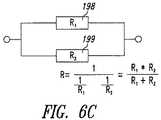
金属ナノワイヤベースの膜およびITO膜を組み合わせることによって、相乗的利点を有する複合膜が可能になる。図6Aは、複合膜186が、基板110(例えば、ガラス)上にITO膜188と、ITO膜188の上に配置されるナノワイヤ膜192とを備え、ナノワイヤ膜192がナノワイヤ194を備えることを示す。 Combining metal nanowire-based films and ITO films allows composite films with synergistic advantages. FIG. 6A shows that the
一実施形態では、ナノワイヤ194の荷重密度は、電気的パーコレーション閾値を下回る。それにもかかわらず、表面伝導率は、ナノワイヤおよび下部ITO膜188の組み合わせによって、複合膜186において確立可能である。上述のように、ITO膜は、ナノワイヤ間の任意の絶縁間隙を充填することが可能である。 In one embodiment, the load density of the
図6Bは、ナノワイヤベースの膜およびITO膜の代替配置を有する複合膜196を示す。図示するように、ナノワイヤ膜192は、最初に基板110上に蒸着される。ITO膜188は、ナノワイヤ膜192の上にスパッタされる。図6Aと同様に、ナノワイヤ194は、必ずしもそれ自体で導電性網を形成するとは限らない。それにもかかわらず、面内導電率は、ナノワイヤおよび下部ITO膜188の組み合わせによって、複合膜196において確立可能である。 FIG. 6B shows a
図示するように、表面および面内導電率を含む複合膜における導電率は、構成膜のみ、すなわち、ナノワイヤベースの膜およびITO膜のいずれかの導電率よりも優れていることが可能である。有利には、構成膜は、相互に補完し、例えば、連続ITO膜の存在による単なる構成膜の単なる相加効果を上回る特性を相乗的に提供し、電圧源への接続時に、複合膜は、ナノワイヤだけに基づく透明導電体の電位よりも均一な電位を有する(図2Bも参照)。一方、ナノワイヤは、導電率の損失を引き起こさずに、複合膜において特定の程度の屈曲を可能にする。例えば、ナノワイヤは、ITO膜のバルク内の微小な割れ目を克服し、導電率を維持することが可能であるため、物理的応力を受ける際に複合膜における潜在的な不具合を防止する。 As shown, the conductivity in the composite film including the surface and in-plane conductivity can be superior to that of either the constituent films alone, ie, the nanowire-based film or the ITO film. Advantageously, the constituent films complement each other and provide, for example, synergistically more properties than just the additive effect of the constituent films due to the presence of the continuous ITO film, and when connected to the voltage source, the composite film is It has a more uniform potential than that of a transparent conductor based on nanowires only (see also FIG. 2B) On the other hand, nanowires allow a certain degree of bending in the composite film without causing a loss of conductivity. For example, nanowires can overcome minute cracks in the bulk of the ITO film and maintain electrical conductivity, thus preventing potential failures in the composite film when subjected to physical stress.
加えて、ナノワイヤの高導電率により、複合膜の高導電率は、同一の厚さの純粋ITO膜の導電率に比べてかなり高いことが可能である。ゆえに、構成要素として純粋ITO膜よりも薄いITO膜であって、依然として、純粋で厚いITO膜と同一レベルの導電性を達成可能であるITOを有する複合膜を生成することが可能である。ITO膜の厚さを縮小することによって、加工費用が直接的に減少可能になり、また、ITO膜が破損する可能性が低くなる。 In addition, due to the high conductivity of the nanowires, the high conductivity of the composite film can be significantly higher than that of a pure ITO film of the same thickness. Therefore, it is possible to produce a composite film having ITO that is thinner than a pure ITO film as a constituent element and still having the same level of conductivity as a pure and thick ITO film. By reducing the thickness of the ITO film, the processing cost can be directly reduced, and the possibility that the ITO film is damaged is reduced.
さらに、図6Aおよび図6Bの構成膜は、2つの並列抵抗器に類似する配置にあるが、複合膜の抵抗率が、並列抵抗器について予測される抵抗率よりも低くなり得ることが認められる(実施例4も参照)。図6Cは、2つの並列抵抗器198(抵抗率R1)および199(抵抗率R2)を図式的に示す。既知のように、1組の並列抵抗器の全体抵抗率Rは、
R=(R1xR2)/(R1+R2)
である。In addition, it is recognized that the constituent films of FIGS. 6A and 6B are in an arrangement similar to two parallel resistors, but the resistivity of the composite film can be lower than that expected for the parallel resistors. (See also Example 4). FIG. 6C schematically shows two parallel resistors 198 (resistivity R1) and 199 (resistivity R2). As is known, the overall resistivity R of a set of parallel resistors is
R = (R1xR2) / (R1 + R2)
It is.
実施例4は、250Ω/□の抵抗率を有するITO膜と、約250Ω/□の抵抗率を有するナノワイヤベースの膜とによって形成される複合膜の抵抗率を測定する。これらの2つの構成膜が、単に並列抵抗器であれば、全体抵抗率は、約125Ω/□になるであろう。しかしながら、複合膜の抵抗率は、約50−80Ω/□の範囲であることが観測され、これは、ITO膜(250Ω/□)およびナノワイヤ膜(250Ω/□)の並列抵抗器として予測された抵抗率よりもかなり低い。 Example 4 measures the resistivity of a composite film formed by an ITO film having a resistivity of 250 Ω / □ and a nanowire-based film having a resistivity of about 250 Ω / □. If these two constituent films are simply parallel resistors, the overall resistivity will be about 125 Ω / □. However, the resistivity of the composite film was observed to be in the range of about 50-80Ω / □, which was predicted as a parallel resistor of ITO film (250Ω / □) and nanowire film (250Ω / □). Much lower than resistivity.
任意により、複合膜は、所定の導電率レベルにおいて、ナノワイヤベースの膜のみよりも低い反射性を有することが可能である。上述のように、ナノワイヤのみから形成される透明導電体膜では、ナノワイヤの数の減少により、透明導電体において光散乱の低減がもたらされ得るが、導電率損失の犠牲を潜在的に伴う。本実施形態に従う複合膜により、ITO膜が提供する補足的導電率により、導電率の低下を必ずしも引き起こさずに、数の少ないナノワイヤを用いることによって反射の低減が可能になる。 Optionally, the composite film can have a lower reflectivity than a nanowire-based film alone at a given conductivity level. As described above, in a transparent conductor film formed only from nanowires, a reduction in the number of nanowires can result in a reduction in light scattering in the transparent conductor, but at the cost of a loss of conductivity. With the composite film according to this embodiment, the supplementary conductivity provided by the ITO film allows a reduction in reflection by using fewer nanowires without necessarily causing a decrease in conductivity.
図6Aおよび図6BのITO膜の代わりに、他の金属酸化物膜を使用することが可能である。例示的な金属酸化物膜には、ドープ酸化亜鉛膜、フッ素ドープ酸化スズ膜、アルミニウムドープ酸化亜鉛膜、Zn2SnO4、ZnSnO3、MgIn2O4、GalnO3、(Ga2ln)2O3、Zn2In2O5、ln4Sn3O12等が含まれる。Crawford, G.P.、Flexible Flat Panel Display(John Wiley and Sons,2005)。Other metal oxide films can be used in place of the ITO films of FIGS. 6A and 6B. Exemplary metal oxide films include doped zinc oxide films, fluorine-doped tin oxide films, aluminum-doped zinc oxide films, Zn2 SnO4 , ZnSnO3 , MgIn2 O4 , GalnO3 , (Ga2 ln)2 O3 , Zn2 In2 O5 , ln4 Sn3 O12 and the like. Crawford, G.M. P. , Flexible Flat Panel Display (John Wiley and Sons, 2005).
典型的には、金属ナノワイヤ(例えば、銀ナノワイヤ)および金属酸化物膜の組み合わせに基づく複合透明導電体は、少なくとも50%、少なくとも60%、少なくとも70%、または少なくとも80%、または少なくとも85%、または少なくとも90%、または少なくとも95%(参照として空気を使用)の光透過性を有する。 Typically, composite transparent conductors based on a combination of metal nanowires (eg, silver nanowires) and metal oxide films are at least 50%, at least 60%, at least 70%, or at least 80%, or at least 85%, Or at least 90%, or at least 95% (using air as a reference).
典型的には、金属ナノワイヤ(例えば、銀ナノワイヤ)および金属酸化物膜の組み合わせに基づく複合透明導電体は、1−108Ω/□の範囲のシート抵抗を有し、複合透明導電体の最終用途に依存する。より典型的には、シート抵抗は、10Ω/□から1000Ω/□、100Ω/□から750Ω/□、50Ω/□から200Ω/□、100Ω/□から500Ω/□、または100Ω/□から250Ω/□、10Ω/□から200Ω/□、10Ω/□から50Ω/□、または1Ω/□から10Ω/□の範囲である。Typically, composite transparent conductors based on a combination of metal nanowires (eg, silver nanowires) and metal oxide films have sheet resistances in the range of 1-108 Ω / □, and the final composite transparent conductor Depends on application. More typically, the sheet resistance is 10Ω / □ to 1000Ω / □, 100Ω / □ to 750Ω / □, 50Ω / □ to 200Ω / □, 100Ω / □ to 500Ω / □, or 100Ω / □ to 250Ω / □. The range is 10Ω / □ to 200Ω / □, 10Ω / □ to 50Ω / □, or 1Ω / □ to 10Ω / □.
好適な実施形態では、金属ナノワイヤ(例えば、銀ナノワイヤ)および金属酸化物膜の組み合わせに基づく複合透明導電体は、85%より高い光透過性および1000Ω/□未満のシート抵抗を有する。他の実施形態では、金属ナノワイヤ(例えば、銀ナノワイヤ)および金属酸化物膜の組み合わせに基づく複合透明導電体は、95%より高い光透過性および500Ω/□未満のシート抵抗を有する。他の実施形態では、金属ナノワイヤ(例えば、銀ナノワイヤ)および金属酸化物膜の組み合わせに基づく複合透明導電体は、90%より高い光透過性および100Ω/□未満のシート抵抗を有する。他の実施形態では、金属ナノワイヤ(例えば、銀ナノワイヤ)および金属酸化物膜の組み合わせに基づく複合透明導電体は、85%より高い光透過性および50Ω/□未満のシート抵抗を有する。 In a preferred embodiment, a composite transparent conductor based on a combination of metal nanowires (eg, silver nanowires) and metal oxide films has a light transmission greater than 85% and a sheet resistance of less than 1000Ω / □. In other embodiments, a composite transparent conductor based on a combination of metal nanowires (eg, silver nanowires) and metal oxide films has a light transmission greater than 95% and a sheet resistance less than 500 Ω / □. In other embodiments, a composite transparent conductor based on a combination of metal nanowires (eg, silver nanowires) and metal oxide films has a light transmission greater than 90% and a sheet resistance of less than 100Ω / □. In other embodiments, a composite transparent conductor based on a combination of metal nanowires (eg, silver nanowires) and a metal oxide film has a light transmission greater than 85% and a sheet resistance of less than 50Ω / □.
(4.二次導電性媒体としての導電性ポリマー膜)
別の実施形態では、複合透明導電体は、二次導電性媒体と組み合わせられる複数の金属ナノワイヤを備え、二次導電性媒体は、連続ポリマー膜である。(4. Conductive polymer film as secondary conductive medium)
In another embodiment, the composite transparent conductor comprises a plurality of metal nanowires combined with a secondary conductive medium, wherein the secondary conductive medium is a continuous polymer film.
特定のポリマーは、連続的に重複する軌道の共役骨格における電子非局在化により導電性である。例えば、単一および2重の炭素−炭素結合の交互から形成されるポリマーは、電子が占有可能である重複p軌道の連続経路を提供することが可能である。 Certain polymers are conductive due to electron delocalization in the conjugation backbone of continuously overlapping orbitals. For example, a polymer formed from alternating single and double carbon-carbon bonds can provide a continuous path of overlapping p-orbitals that can be occupied by electrons.
共通の種類の有機導電性ポリマーには、ポリ(アセチレン)、ポリ(ピロール)、ポリ(チオフェン)、ポリ(アニリン)、ポリ(フルオレン)、ポリ(3−アルキルチオフェン)、PEDOTとしても既知であるポリ(3,4−エチレンジオキシチオフェン)、ポリテトラチアフルバレン、ポリナフタレン、ポリパラフェニレン、ポリ(パラフェニレンスルフィド)、およびポリ(パラフェニレンビニレン)が含まれるが、これらに限定されない。 Common types of organic conductive polymers are also known as poly (acetylene), poly (pyrrole), poly (thiophene), poly (aniline), poly (fluorene), poly (3-alkylthiophene), PEDOT Examples include, but are not limited to, poly (3,4-ethylenedioxythiophene), polytetrathiafulvalene, polynaphthalene, polyparaphenylene, poly (paraphenylene sulfide), and poly (paraphenylene vinylene).
導電性ポリマー膜単独では、典型的には導電性ではなく、または表示機器における透明導電体として機能するには十分物理的に強固ではないが、導電性ポリマー膜は、金属ナノワイヤと組み合わせまたはドープして、複合透明導電体を形成することが可能である。複合透明導電体は、主要な電流伝導媒体としての金属ナノワイヤと、電場を均一にするためのフィルタとしての導電性ポリマー膜とに依存することが可能である。加えて、金属ナノワイヤは、導電性ポリマー膜の機械的特性を補強および強化することも可能である。 Conductive polymer films alone are typically not conductive or physically strong enough to function as transparent conductors in display devices, but conductive polymer films are combined or doped with metal nanowires. Thus, a composite transparent conductor can be formed. Composite transparent conductors can rely on metal nanowires as the primary current conducting medium and conductive polymer films as filters to make the electric field uniform. In addition, metal nanowires can also reinforce and enhance the mechanical properties of conductive polymer films.
任意により、導電性ポリマー膜は、複合膜の吸収特性も調整することが可能である。 Optionally, the conductive polymer film can also adjust the absorption characteristics of the composite film.
図7Aは、複合膜200が、基板110(例えば、ガラス)上に導電性ポリマー膜204と、導電性ポリマー膜204の上に配置されるナノワイヤ膜220とを備えることを示す。 FIG. 7A shows that the
図7Bは、ナノワイヤベースの膜および導電性ポリマー膜の代替配置を有する複合膜230を示す。図示するように、ナノワイヤ膜220は、最初に基板110上に蒸着される。導電性ポリマー膜104は、ナノワイヤ膜220の上面の上に蒸着される。図6Aと同様に、ナノワイヤ224は、必ずしもそれ自体で導電性網を形成するとは限らない。それにもかかわらず、面内導電率は、ナノワイヤおよび下部導電性ポリマー膜204の組み合わせによって、複合膜230において確立可能である。 FIG. 7B shows a
代替実施形態では、最初に金属ナノワイヤを基板上に蒸着して、導電性網を形成する。導電性ポリマー膜は、電極として金属ナノワイヤ網を使用して原位置で形成可能である。原位置で形成可能である適切な導電性ポリマーの例として、ポリピロールが挙げられる。より具体的には、ナノワイヤベースの導電性網を電極(すなわち、陽極)として使用して、ピロール単量体は、電気化学的に重合することが可能であり、導電性網上に塗膜を形成することが可能である。また、導電性ポリマー膜は、当技術分野において既知の方法の存在下で化学的に形成可能である。結果として生じる複合透明導電体は、導電性ポリマー膜に埋め込まれるナノワイヤを特徴とする。 In an alternative embodiment, metal nanowires are first deposited on the substrate to form a conductive network. The conductive polymer film can be formed in situ using a metal nanowire network as an electrode. An example of a suitable conductive polymer that can be formed in situ is polypyrrole. More specifically, using a nanowire-based conductive network as an electrode (ie, an anode), the pyrrole monomer can be polymerized electrochemically and a coating is formed on the conductive network. It is possible to form. Also, the conductive polymer film can be chemically formed in the presence of methods known in the art. The resulting composite transparent conductor features nanowires embedded in a conductive polymer film.
典型的には、金属ナノワイヤ(例えば、銀ナノワイヤ)および導電性ポリマー膜の組み合わせに基づく複合透明導電体は、少なくとも50%、少なくとも60%、少なくとも70%、または少なくとも80%、または少なくとも85%、または少なくとも90%、または少なくとも95%(参照として空気を使用)の光透過性を有する。 Typically, a composite transparent conductor based on a combination of metal nanowires (eg, silver nanowires) and a conductive polymer film is at least 50%, at least 60%, at least 70%, or at least 80%, or at least 85%, Or at least 90%, or at least 95% (using air as a reference).
典型的には、金属ナノワイヤ(例えば、銀ナノワイヤ)および導電性ポリマー膜の組み合わせに基づく複合透明導電体は、1−108Ω/□の範囲のシート抵抗を有し、複合透明導電体の最終用途に依存する。より典型的には、シート抵抗は、10Ω/□から1000Ω/□、100Ω/□から750Ω/□、50Ω/□から200Ω/□、100Ω/□から500Ω/□、または100Ω/□から250Ω/□、10Ω/□から200Ω/□、10Ω/□から50Ω/□、または1Ω/□から10Ω/□の範囲である。Typically, a composite transparent conductor based on a combination of metal nanowires (eg, silver nanowires) and a conductive polymer film has a sheet resistance in the range of 1-108 Ω / □ and the final composite transparent conductor Depends on application. More typically, the sheet resistance is 10Ω / □ to 1000Ω / □, 100Ω / □ to 750Ω / □, 50Ω / □ to 200Ω / □, 100Ω / □ to 500Ω / □, or 100Ω / □ to 250Ω / □. The range is 10Ω / □ to 200Ω / □, 10Ω / □ to 50Ω / □, or 1Ω / □ to 10Ω / □.
好適な実施形態では、金属ナノワイヤ(例えば、銀ナノワイヤ)および導電性ポリマー膜の組み合わせに基づく複合透明導電体は、85%より高い光透過性および1000Ω/□未満のシート抵抗を有する。他の実施形態では、金属ナノワイヤ(例えば、銀ナノワイヤ)導電性ポリマー膜の組み合わせに基づく複合透明導電体は、95%より高い光透過性および500Ω/□未満のシート抵抗を有する。他の実施形態では、金属ナノワイヤ(例えば、銀ナノワイヤ)および導電性ポリマー膜の組み合わせに基づく複合透明導電体は、90%より高い光透過性および100Ω/□未満のシート抵抗を有する。他の実施形態では、金属ナノワイヤ(例えば、銀ナノワイヤ)および導電性ポリマー膜の組み合わせに基づく複合透明導電体は、85%より高い光透過性および50Ω/□未満のシート抵抗を有する。 In a preferred embodiment, a composite transparent conductor based on a combination of metal nanowires (eg, silver nanowires) and a conductive polymer film has a light transmission greater than 85% and a sheet resistance of less than 1000Ω / □. In other embodiments, a composite transparent conductor based on a combination of metal nanowire (eg, silver nanowire) conductive polymer films has a light transmission greater than 95% and a sheet resistance of less than 500 Ω / □. In other embodiments, a composite transparent conductor based on a combination of metal nanowires (eg, silver nanowires) and a conductive polymer film has a light transmission greater than 90% and a sheet resistance of less than 100Ω / □. In other embodiments, a composite transparent conductor based on a combination of metal nanowires (eg, silver nanowires) and a conductive polymer film has a light transmission greater than 85% and a sheet resistance less than 50Ω / □.
(電気的特性および光学的特性)
本明細書において論じるように、複合透明導電体において組み合わせられた導電性媒体は、個々の導電性媒体をまとめるよりも、予想外の特質または強化された特性を提供する。複合透明導電体のこれらの相乗的な改善には、より一様な電位(電源への接続時)、より高い導電率、より良好な耐久性、より高いコントラスト比等が含まれるが、これらに限定されない。(Electrical and optical characteristics)
As discussed herein, conductive media combined in composite transparent conductors provide unexpected properties or enhanced properties rather than grouping individual conductive media. These synergistic improvements in composite transparent conductors include more uniform potential (when connected to power supply), higher conductivity, better durability, higher contrast ratio, etc. It is not limited.
典型的には、金属ナノワイヤ(例えば、銀ナノワイヤ)および二次導電性媒体の組み合わせに基づく複合透明導電体は、少なくとも50%、少なくとも60%、少なくとも70%、または少なくとも80%、または少なくとも85%、または少なくとも90%、または少なくとも95%(参照として空気を使用)の光透過性を有する。ヘーズは、光散乱の指標である。これは、入射光から分離し、かつ透過中に散乱した光の量の割合を指す(すなわち、透過ヘーズ)。主に媒体の特性である光透過性とは違って、ヘーズは、しばしば製造に関し、典型的には、表面粗さおよび埋め込み粒子または媒体中の成分不均質によって引き起こされる。種々の実施形態では、透明導電体のヘーズは、10%以下、8%以下、5%以下、3%以下、または1%以下である。 Typically, composite transparent conductors based on a combination of metal nanowires (eg, silver nanowires) and secondary conductive media are at least 50%, at least 60%, at least 70%, or at least 80%, or at least 85% Or at least 90%, or at least 95% (using air as a reference). Haze is an indicator of light scattering. This refers to the proportion of the amount of light that is separated from the incident light and scattered during transmission (ie, transmission haze). Unlike light transmission, which is primarily a property of the media, haze is often related to manufacturing and is typically caused by surface roughness and embedded particles or component inhomogeneities in the media. In various embodiments, the haze of the transparent conductor is 10% or less, 8% or less, 5% or less, 3% or less, or 1% or less.
典型的には、金属ナノワイヤ(例えば、銀ナノワイヤ)および二次導電性媒体の組み合わせに基づく複合透明導電体は、1−108Ω/□の範囲のシート抵抗を有し、複合透明導電体の最終用途に依存する。より典型的には、シート抵抗は、10Ω/□から1000Ω/□、100Ω/□から750Ω/□、50Ω/□から200Ω/□、100Ω/□から500Ω/□、または100Ω/□から250Ω/□、10Ω/□から200Ω/□、10Ω/□から50Ω/□、または1Ω/□から10Ω/□の範囲である。Typically, a composite transparent conductor based on a combination of metal nanowires (eg, silver nanowires) and a secondary conductive medium has a sheet resistance in the range of 1-108 Ω / □, Depends on end use. More typically, the sheet resistance is 10Ω / □ to 1000Ω / □, 100Ω / □ to 750Ω / □, 50Ω / □ to 200Ω / □, 100Ω / □ to 500Ω / □, or 100Ω / □ to 250Ω / □. The range is 10Ω / □ to 200Ω / □, 10Ω / □ to 50Ω / □, or 1Ω / □ to 10Ω / □.
好適な実施形態では、金属ナノワイヤ(例えば、銀ナノワイヤ)および二次導電性媒体の組み合わせに基づく複合透明導電体は、85%より高い光透過性および1000Ω/□未満のシート抵抗を有する。他の実施形態では、金属ナノワイヤ(例えば、銀ナノワイヤ)および二次導電性媒体の組み合わせに基づく複合透明導電体は、95%より高い光透過性および500Ω/□未満のシート抵抗を有する。他の実施形態では、金属ナノワイヤ(例えば、銀ナノワイヤ)および二次導電性媒体の組み合わせに基づく複合透明導電体は、90%より高い光透過性および100Ω/□未満のシート抵抗を有する。他の実施形態では、金属ナノワイヤ(例えば、銀ナノワイヤ)および二次導電性媒体の組み合わせに基づく複合透明導電体は、85%より高い光透過性および50Ω/□未満のシート抵抗を有する。 In a preferred embodiment, a composite transparent conductor based on a combination of metal nanowires (eg, silver nanowires) and secondary conductive media has a light transmission greater than 85% and a sheet resistance less than 1000 Ω / □. In other embodiments, a composite transparent conductor based on a combination of metal nanowires (eg, silver nanowires) and a secondary conductive medium has a light transmission greater than 95% and a sheet resistance less than 500Ω / □. In other embodiments, a composite transparent conductor based on a combination of metal nanowires (eg, silver nanowires) and a secondary conductive medium has a light transmission greater than 90% and a sheet resistance of less than 100Ω / □. In other embodiments, a composite transparent conductor based on a combination of metal nanowires (eg, silver nanowires) and a secondary conductive medium has a light transmission greater than 85% and a sheet resistance less than 50Ω / □.
本明細書に説明する複合透明導電体は、フラットパネルディスプレイにおいて電極として適切である電気的特性および光学的特性を有することが可能である。フラットパネルディスプレイにおける透明電極のシート抵抗の典型的な範囲は、約10−100Ω/□であり、層の透過性は、87%より高い(参照としてガラスを使用する場合)か、または95%より高い(参照として空気を使用する場合)。 The composite transparent conductors described herein can have electrical and optical properties that are suitable as electrodes in flat panel displays. The typical range of sheet resistance of transparent electrodes in flat panel displays is about 10-100 Ω / □, and the transparency of the layer is higher than 87% (when using glass as a reference) or higher than 95% High (when using air as a reference).
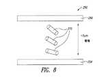
さらに、電極として使用する場合、複合透明導電体は、液晶ディスプレイ(LCD)において特に有利である一様な電場を提供する。図8は、LCD設定250を図式的に示し、本設定において、画素電極254および対電極260は、約3−5μm離隔し、これは「セルギャップ」とも呼ばれる。液晶セル270は、2つの電極の間に配置される。簡潔に言うと、LCDは、セルに閉じ込められる液晶分子が、2つの電極間に生成された印加電場に応答して、その構造を変化させる際に動作する。 Furthermore, when used as an electrode, the composite transparent conductor provides a uniform electric field that is particularly advantageous in liquid crystal displays (LCDs). FIG. 8 schematically shows an LCD setting 250 in which the
ナノワイヤのみから形成される透明導電体電極を使用する場合、所望のレベルの導電率および光透過性において、ナノワイヤ間の空間は、液晶セルキャップ(すなわち、「セルギャップ」)に相当し得る。したがって、セルにおける全ての液晶分子が、同一の電場(大きさおよび方向の両方)によって駆動されるわけではなく、それによって、セルの光学的特性における不要な不均一性がもたらされる可能性がある。 When using transparent conductor electrodes formed only from nanowires, at the desired level of conductivity and light transmission, the space between nanowires can correspond to a liquid crystal cell cap (ie, a “cell gap”). Thus, not all liquid crystal molecules in a cell are driven by the same electric field (both magnitude and direction), which can lead to unwanted non-uniformities in the optical properties of the cell. .
しかしながら、電極として複合透明導電体を用いることによって、ナノワイヤ間の空間が効率的に低減または排除される。典型的には、ナノワイヤ間のメッシュサイズは、液晶セルギャップの1/5未満であるべきである。より典型的には、メッシュサイズは、セルギャップの1/10または1/100未満であるべきである。二次導電性媒体の存在によって、一様な電極場が液晶セルにおいて印加可能になり、液晶分子の一様配向がもたらされるため、均質な光学的応答がもたらされる。 However, by using a composite transparent conductor as an electrode, the space between nanowires is efficiently reduced or eliminated. Typically, the mesh size between nanowires should be less than 1/5 of the liquid crystal cell gap. More typically, the mesh size should be less than 1/10 or 1/100 of the cell gap. The presence of the secondary conductive medium allows a uniform electrode field to be applied in the liquid crystal cell, resulting in a uniform orientation of the liquid crystal molecules, resulting in a uniform optical response.
図示するように、LCDセルにおける電極が、ナノワイヤのみを備える場合、セルギャップの1/5−1/100のメッシュサイズを可能にする表面荷重レベルは、高ヘーズおよび低コントラスト比を含む不十分な光学的特性をもたらす。しかしながら、複合透明導電体を電極として使用すると、一次導電性媒体の金属ナノワイヤ(または、金属ナノチューブ)は、セルギャップと類似するメッシュサイズを維持し、一方、二次導電性媒体は、セルギャップの約1/5−1/100にメッシュサイズを低減するか、または連続導電性薄膜の場合、メッシュサイズを排除する。結果として生じるLCDセルは、電極の光学的特性が改善するため、改善されたセル性能を有する。 As shown, if the electrodes in the LCD cell comprise only nanowires, the surface load level that allows a mesh size of 1 / 5-1 / 100 of the cell gap is insufficient, including high haze and low contrast ratio Provides optical properties. However, when composite transparent conductors are used as electrodes, the metal nanowires (or metal nanotubes) in the primary conductive medium maintain a mesh size similar to the cell gap, while the secondary conductive medium is in the cell gap. Reduce the mesh size to about 1 / 5-1 / 100 or eliminate the mesh size for continuous conductive thin films. The resulting LCD cell has improved cell performance due to improved electrode optical properties.
したがって、一実施形態は、第1の電極と、第2の電極であって、第1の電極および第2の電極間の垂直距離は、セルギャップを規定する第2の電極とを液晶セルに提供し、第1の電極は、一次導電性媒体および二次導電性媒体を含む複合透明導電体であり、一次導電性媒体は、セルギャップと類似のメッシュサイズを有する金属ナノワイヤまたは金属ナノチューブを含み、二次導電性媒体は、連続導電性薄膜またはセルギャップの約1/5から1/100のメッシュサイズを有するナノ構造の導電性網である。 Therefore, in one embodiment, the first electrode and the second electrode, and the vertical distance between the first electrode and the second electrode is different from the second electrode that defines the cell gap in the liquid crystal cell. The first electrode is a composite transparent conductor comprising a primary conductive medium and a secondary conductive medium, the primary conductive medium comprising metal nanowires or metal nanotubes having a mesh size similar to the cell gap; The secondary conductive medium is a continuous conductive thin film or a nanostructured conductive network having a mesh size of about 1/5 to 1/100 of the cell gap.
典型的には、セルギャップは、約3−5μmである。特定の実施形態では、ナノ構造の導電性網は、セルギャップの約1/5から1/10、またはセルギャップの約1/10から1/100のメッシュサイズを有する。 Typically, the cell gap is about 3-5 μm. In certain embodiments, the nanostructured conductive network has a mesh size of about 1/5 to 1/10 of the cell gap, or about 1/10 to 1/100 of the cell gap.
上述の複合透明導電体のいずれかは、液晶セルの第1の電極として使用可能である。例えば、種々の実施形態では、一次導電性媒体は、金属ナノワイヤ(例えば、銀ナノワイヤ)または金属ナノチューブ(例えば、金ナノチューブ)であることが可能である。好適な実施形態では、金属ナノワイヤまたは金属ナノチューブは、20−80nmの直径(ナノチューブでは外径)を有し、5−30μmの長さを有する。 Any of the composite transparent conductors described above can be used as the first electrode of the liquid crystal cell. For example, in various embodiments, the primary conductive medium can be a metal nanowire (eg, silver nanowire) or a metal nanotube (eg, gold nanotube). In a preferred embodiment, the metal nanowire or metal nanotube has a diameter of 20-80 nm (outer diameter for a nanotube) and a length of 5-30 μm.
二次導電性媒体は、カーボンナノチューブ、一次導電性媒体の金属ナノワイヤとは異なる金属ナノワイヤ、または一次導電性媒体の金属ナノチューブとは異なる金属ナノチューブの導電性網を含み得る。 The secondary conductive medium may include a carbon nanotube, a metal nanowire that is different from the metal nanowire of the primary conductive medium, or a conductive network of metal nanotubes that is different from the metal nanotube of the primary conductive medium.
代替として、二次導電性媒体は、金属酸化物膜(例えば、ITO膜)または導電性ポリマー膜(例えば、PEDOT膜)等の連続導電性薄膜であることが可能である。 Alternatively, the secondary conductive medium can be a continuous conductive thin film such as a metal oxide film (eg, ITO film) or a conductive polymer film (eg, PEDOT film).
さらなる実施形態では、本明細書において説明するように、第2の電極も複合透明導電体であることが可能である。 In further embodiments, the second electrode can also be a composite transparent conductor, as described herein.
特定の実施形態では、第1の電極は、80−95%の光透過性を有する。 In certain embodiments, the first electrode has 80-95% light transmission.
上述のように、複合透明導電体は、典型的には金属ナノワイヤと関連する不要なレベルの散乱を低減するように設計可能である。二次導電性媒体は、電流を伝導するため、所定の導電率を達成するのに必要なナノワイヤの数が少なくなる。加えて、本明細書に説明する二次導電性媒体は、典型的には非反射性、低反射性、または散乱断面が小さいナノ構造を備え、結果として、存在するナノワイヤの数が少なくなるため、全体の散乱は減少する。 As described above, composite transparent conductors can be designed to reduce unwanted levels of scattering typically associated with metal nanowires. Since the secondary conductive medium conducts current, fewer nanowires are needed to achieve a given conductivity. In addition, the secondary conductive media described herein typically include nanostructures that are non-reflective, low-reflective, or have a small scattering cross section, resulting in fewer nanowires present. , The overall scattering is reduced.
(追加の層)
さらなる実施形態では、オーバーコートの不活性層が、複合透明導電体を安定化および保護するために蒸着可能である。また、オーバーコートは、防幻特性および防反射特性等の好ましい光学的特性も提供することが可能であり、ナノ粒子の反射率をさらに低減させる役割を果たす。(Additional layer)
In a further embodiment, an overcoat inert layer can be deposited to stabilize and protect the composite transparent conductor. The overcoat can also provide favorable optical properties such as anti-glare properties and anti-reflection properties, and serves to further reduce the reflectivity of the nanoparticles.
したがって、オーバーコートは、ハードコート、反射防止層、保護膜、障壁層、およびその同等物のうちの1つ以上であることが可能であり、その全てについて、同時係属出願第11/871,767号および第11/504,822号において広範囲に説明される。 Thus, the overcoat can be one or more of a hard coat, an antireflective layer, a protective film, a barrier layer, and the like, all of which are co-pending application Ser. No. 11 / 871,767. And 11 / 504,822 are extensively described.
適切なハードコートの例として、ポリアクリル酸、エポキシ樹脂、ポリウレタン、ポリシラン、シリコーン、ポリ(シリコアクリル)等の合成ポリマーが挙げられる。適切な防幻材料は、当技術分野において周知であり、シロキサン、ポリスチレン/PMMA混合物、ラッカー(例えば、酢酸ブチル/ニトロセルロース/ろう/アルキド樹脂)、ポリチオフェン、ポリピロール、ポリウレタン、ニトロセルロース、およびアクリレートが含まれるがこれらに限定されず、その全ては、コロイド状シリカまたはヒュームドシリカ等の光拡散材料を含み得る。保護膜の例として、ポリエステル、ポリエチレンテレフタレート(PET)、ポリブチレンテレフタレート、ポリメチルメタクリレート(PMMA)、アクリル樹脂、ポリカーボネート(PC)、ポリスチレン、トリアセテート(TAC)、ポリビニルアルコール、ポリ塩化ビニル、ポリ塩化ビニリデン、ポリエチレン、エチレン酢酸ビニル共重合体、ポリビニルブチラール、金属イオン架橋エチレン−メタクリル酸共重合体、ポリウレタン、セロファン、ポリオレフィン、またはその同等物が挙げられるが、これらに限定されず、特に、PET、PC、PMMA、またはTACが好ましい。 Examples of suitable hard coats include synthetic polymers such as polyacrylic acid, epoxy resin, polyurethane, polysilane, silicone, poly (silicoacrylic) and the like. Suitable antiglare materials are well known in the art and include siloxanes, polystyrene / PMMA mixtures, lacquers (eg, butyl acetate / nitrocellulose / wax / alkyd resins), polythiophenes, polypyrroles, polyurethanes, nitrocellulose, and acrylates. Including but not limited to, all of which may include light diffusing materials such as colloidal silica or fumed silica. Examples of protective films include polyester, polyethylene terephthalate (PET), polybutylene terephthalate, polymethyl methacrylate (PMMA), acrylic resin, polycarbonate (PC), polystyrene, triacetate (TAC), polyvinyl alcohol, polyvinyl chloride, polyvinylidene chloride , Polyethylene, ethylene vinyl acetate copolymer, polyvinyl butyral, metal ion cross-linked ethylene-methacrylic acid copolymer, polyurethane, cellophane, polyolefin, or the like, but not limited thereto, in particular, PET, PC , PMMA, or TAC is preferred.
(パターン化)
本明細書に説明する複合透明導電体は、その最終用途に応じてパターン化可能である。当技術分野における任意の既知の方法ならびに共有および同時係属の米国特許出願第11/504,822号、同第11/871,767号において説明するパターン化方法は、複合透明導電体のパターン化に使用可能である。(Patterned)
The composite transparent conductor described herein can be patterned depending on its end use. Any known method in the art and the patterning method described in co-pending and co-pending U.S. Patent Application Nos. 11 / 504,822 and 11 / 871,767 are useful for patterning composite transparent conductors. It can be used.
(複合透明導電体の用途)
本明細書に説明する複合透明導電体は、金属酸化物膜(例えば、ITO)を現在利用する全ての機器を含む多種多様の機器における透明電極、偏光子、色フィルタ等の機能性膜として使用可能である。図7は、ハウジング258において複合透明導電体254を含む機器250を図式的に示す。複合透明導電体は、一次導電性媒体(すなわち、複数の金属ナノワイヤ)および第2の導電性媒体(すなわち、連続導電性薄膜)の上述の構成または組み合わせのうちのいずれかであることが可能である。(Use of composite transparent conductor)
The composite transparent conductor described herein is used as a functional film for transparent electrodes, polarizers, color filters, etc. in a wide variety of devices, including all devices that currently use metal oxide films (eg, ITO). Is possible. FIG. 7 schematically shows a
適切な機器の例として、LCD等のフラットパネルディスプレイ、プラズマディスプレイパネル(PDP)、カラーフラットパネルディスプレイ用の色フィルタ上の塗膜、タッチスクリーン、電磁干渉、電磁遮蔽、機能性ガラス(例えば、エレクトロクロミック窓用)、ELランプおよび太陽電池を含む光電子機器、ならびにその同等物が挙げられる。加えて、本明細書における透明導電体は、フレキシブルディスプレイおよびタッチスクリーン等の可塑性機器に使用可能である。同時係属出願第11/871,767号を参照されたい。 Examples of suitable equipment include flat panel displays such as LCDs, plasma display panels (PDP), coatings on color filters for color flat panel displays, touch screens, electromagnetic interference, electromagnetic shielding, functional glass (eg, electro Chromic windows), optoelectronic devices including EL lamps and solar cells, and the like. In addition, the transparent conductor in this specification can be used for plastic devices such as flexible displays and touch screens. See copending application Ser. No. 11 / 871,767.
(実施例1)
(銀ナノワイヤの合成)
ポリビニルピロリドン(PVP)の存在下でエチレングリコール中に溶解された硝酸銀の還元によって、銀ナノワイヤを合成した。本方法は、例えば、Y.Sun、B.Gates、B.MayersおよびY.Xia、「Crystalline silver nanowires by soft solution processing」、Nanolett、(2002)、2(2)165−168に説明されている。一様な銀ナノワイヤは、遠心分離または他の既知の方法によって選択的に分離可能である。Example 1
(Synthesis of silver nanowires)
Silver nanowires were synthesized by reduction of silver nitrate dissolved in ethylene glycol in the presence of polyvinylpyrrolidone (PVP). This method is described in, for example, Y.W. Sun, B.M. Gates, B.B. Mayers and Y.M. Xia, “Crystalline silver nanobe by soft solution processing”, Nanolett, (2002), 2 (2) 165-168. Uniform silver nanowires can be selectively separated by centrifugation or other known methods.
代替として、適切なイオン添加剤(例えば、テトラブチルアンモニウムクロリド)を上記反応混合物に添加することによって、一様な銀ナノワイヤを直接合成することが可能である。このように産生された銀ナノワイヤをサイズ選択の分離ステップを行なわずに、直接使用することが可能である。本合成は、本出願の譲受人であるCambrios Technologies Corporation名義の米国仮出願第60/815,627号においてより詳細に説明され、本出願は、その全体が本明細書に組み込まれる。 Alternatively, uniform silver nanowires can be synthesized directly by adding a suitable ionic additive (eg, tetrabutylammonium chloride) to the reaction mixture. The silver nanowires thus produced can be used directly without performing a size selection separation step. This synthesis is described in more detail in US Provisional Application No. 60 / 815,627 in the name of Cambrios Technologies Corporation, the assignee of the present application, which is incorporated herein in its entirety.
以下の例において、70nmから80nmまでの幅および約8μm−25μmの長さを有する銀ナノワイヤを使用した。典型的には、より良好な光学的特性(高透過性および低ヘーズ)は、高アスペクト比ワイヤ(すなわち、より長くかつ細い)により達成可能である。 In the following examples, silver nanowires having a width from 70 nm to 80 nm and a length of about 8 μm-25 μm were used. Typically, better optical properties (high transmission and low haze) can be achieved with high aspect ratio wires (ie, longer and thinner).
(実施例2)
(複合透明導電体の調製)
金属ナノワイヤは、基板あるいはITO膜および導電性ポリマー膜等の連続導電性薄膜上に蒸着する前に、インク組成物に調合されることが可能である。(Example 2)
(Preparation of composite transparent conductor)
The metal nanowires can be formulated into an ink composition before being deposited on a substrate or a continuous conductive thin film such as an ITO film and a conductive polymer film.
ITO膜は、基板上に直接スパッタ可能であり、その後、ナノワイヤ層が蒸着される。代替として、最初にナノワイヤ層を基板上に蒸着し、その後、ナノワイヤ層上に直接ITO膜をスパッタすることが可能である。 The ITO film can be sputtered directly onto the substrate, after which a nanowire layer is deposited. Alternatively, it is possible to first deposit a nanowire layer on the substrate and then sputter an ITO film directly on the nanowire layer.
二次導電性媒体がカーボンナノチューブを含む場合、カーボンナノチューブは、共蒸着のために、金属ナノワイヤと共に同一のインク組成物に調合されることが可能である。代替として、カーボンナノチューブは、金属ナノワイヤの蒸着の前または後に、連続蒸着のために、別々のインク組成物に調合されることが可能である。 When the secondary conductive medium includes carbon nanotubes, the carbon nanotubes can be formulated into the same ink composition with metal nanowires for co-deposition. Alternatively, the carbon nanotubes can be formulated into separate ink compositions for continuous deposition before or after deposition of the metal nanowires.
典型的には、インク組成物は、ナノ構造の分散および/または基板上のナノ構造の固定化を促進する薬剤を含む。これらの薬剤には、界面活性剤、粘度調整剤、およびその同等物が含まれる。インク組成物の調合に関する詳細な説明は、同時係属米国特許出願第11/504,822号に記載されており、本出願は、参照によりその全体が本明細書に組み込まれる。 Typically, the ink composition includes an agent that promotes nanostructure dispersion and / or nanostructure immobilization on the substrate. These agents include surfactants, viscosity modifiers, and the like. A detailed description of the formulation of the ink composition is described in copending US patent application Ser. No. 11 / 504,822, which is hereby incorporated by reference in its entirety.
金属ナノワイヤを蒸着するための典型的なインク組成物には、0.0025重量%から0.1重量%の界面活性剤(例えば、Zonyl(登録商標)FSO−100では、好適な範囲は0.0025重量%から0.05重量%まで)、0.02重量%から4重量%までの粘度調整剤(例えば、ヒドロキシプロピルメチルセルロースまたはHPMCでは、好適な範囲は0.02重量%から0.5重量%まで)、94.5重量%から99.0重量%までの溶媒、および0.05重量%から1.4重量%までの金属ナノワイヤが含まれる。適切な界面活性剤の代表的な例として、Zonyl(登録商標)FSN、Zonyl(登録商標)FSO、Zonyl(登録商標)FSH、トリトン(x100、x114、x45)、ダイノール(604、607)、n−ドデシルb−D−マルトシド、およびノベックが挙げられる。適切な粘度調整剤の例として、ヒドロキシプロピルメチルセルロース(HPMC)、メチルセルロース、キサンタンガム、ポリビニルアルコール、カルボキシメチルセルロース、ヒドロキシエチルセルロースが挙げられる。適切な溶媒の例として、水およびイソプロパノールが挙げられる。 Typical ink compositions for depositing metal nanowires include 0.0025% to 0.1% by weight of a surfactant (eg, for Zonyl® FSO-100, the preferred range is 0.00). 0025 wt% to 0.05 wt%), 0.02 wt% to 4 wt% viscosity modifier (for example, for hydroxypropylmethylcellulose or HPMC, the preferred range is 0.02 wt% to 0.5 wt%) %), 94.5% to 99.0% by weight solvent, and 0.05% to 1.4% by weight metal nanowires. Representative examples of suitable surfactants include Zonyl® FSN, Zonyl® FSO, Zonyl® FSH, Triton (x100, x114, x45), Dinol (604, 607), n -Dodecyl bD-maltoside, and Novec. Examples of suitable viscosity modifiers include hydroxypropyl methylcellulose (HPMC), methylcellulose, xanthan gum, polyvinyl alcohol, carboxymethylcellulose, hydroxyethylcellulose. Examples of suitable solvents include water and isopropanol.
インク組成物は、基板上に形成される最終導電性膜の荷重密度の指標であるナノワイヤの所望の濃度に基づいて調製可能である。 The ink composition can be prepared based on the desired concentration of nanowires that is an indicator of the load density of the final conductive film formed on the substrate.
基板は、その上にナノワイヤが蒸着される任意の材料であることが可能である。基板は、剛性または可塑性であることが可能である。好ましくは、基板は、光学的に透明であり、すなわち、材料の光透過性は、可視領域(400nm−700nm)において少なくとも80%である。 The substrate can be any material on which the nanowires are deposited. The substrate can be rigid or plastic. Preferably, the substrate is optically transparent, i.e. the light transmission of the material is at least 80% in the visible region (400 nm-700 nm).
剛性基板の例として、ガラス、ポリカーボネート、アクリル、およびその同等物が挙げられる。具体的には、無アルカリガラス(例えば、ホウケイ酸塩)、低アルカリガラス、およびゼロ膨脹ガラス−セラミック等の特殊ガラスを使用することが可能である。特殊ガラスは、特に、液晶ディスプレイ(LCD)を含む薄型パネルディスプレイシステムに適切である。 Examples of rigid substrates include glass, polycarbonate, acrylic, and the like. Specifically, it is possible to use special glasses such as alkali-free glass (eg, borosilicate), low alkali glass, and zero expansion glass-ceramic. Special glass is particularly suitable for thin panel display systems including liquid crystal displays (LCDs).
可塑性基板の例として、ポリエステル(例えば、ポリエチレンテレフタレート(PET)、ポリエステルナフタレート、およびポリカーボネート)、ポリオレフィン(例えば、直鎖、分岐、および環状ポリオレフィン)、ポリビニル(例えば、ポリ塩化ビニル、ポリ塩化ビニリデン、ポリビニルアセタール、ポリスチレン、ポリアクリル、およびその同等物)、セルロースエステル塩基(例えば、セルローストリアセテート、酢酸セルロース)、ポリエーテルスルホン等のポリスルホン、ポリイミド、シリコーン、および他の従来のポリマー膜が挙げられるが、これらに限定されない。 Examples of plastic substrates include polyesters (eg, polyethylene terephthalate (PET), polyester naphthalate, and polycarbonate), polyolefins (eg, linear, branched, and cyclic polyolefins), polyvinyls (eg, polyvinyl chloride, polyvinylidene chloride, Polyvinyl acetal, polystyrene, polyacryl, and the like), cellulose ester bases (eg, cellulose triacetate, cellulose acetate), polysulfones such as polyethersulfone, polyimides, silicones, and other conventional polymer membranes, It is not limited to these.
インク組成物は、例えば、同時係属米国特許出願第11/504,822号に説明する方法に従って、基板上に蒸着可能である。 The ink composition can be deposited on the substrate, for example, according to the method described in copending US patent application Ser. No. 11 / 504,822.
具体的な例として、銀ナノワイヤの水分散液、すなわち、インク組成物を最初に調製した。銀ナノワイヤの幅は、約35nmから45nmであり、長さは、約10μmであった。インク組成物は、0.2重量%の銀ナノワイヤ、0.4重量%のHPMC、および0.025重量%のトリトンx100を含む。次いで、60秒間500rpmの速度で、ガラス上にインクをスピンコートし、その後、90秒間50℃でポストベーキングし、90秒間180℃でポストベーキングした。塗膜の抵抗率は、約20オーム/スクエアであり、透過性は96%(参照としてガラスを使用)、ヘーズは3.3%であった。 As a specific example, an aqueous dispersion of silver nanowires, that is, an ink composition was first prepared. The width of the silver nanowire was about 35 nm to 45 nm and the length was about 10 μm. The ink composition comprises 0.2 wt% silver nanowires, 0.4 wt% HPMC, and 0.025 wt% Triton x100. The ink was then spin coated onto the glass at a speed of 500 rpm for 60 seconds, followed by post-baking at 50 ° C. for 90 seconds and post-baking at 180 ° C. for 90 seconds. The resistivity of the coating was about 20 ohms / square, the permeability was 96% (using glass as a reference), and the haze was 3.3%.
当業者が理解するように、他の蒸着技法を用いることが可能である。例えば、狭いチャネルにより測定される沈降流動、ダイ流動、傾斜上の流動、スリットコーティング、グラビアコーティング、マイクログラビアコーティング、ビーズコーティング、浸漬コーティング、スロットダイコーティング、およびその同等物が挙げられる。また、印刷手法を使用して、パターン化を含むまたは含まずに、インク組成物を基板上に直接印刷することが可能である。例えば、インクジェット、フレキソ印刷、およびスクリーン印刷を用いることが可能である。 Other vapor deposition techniques can be used as will be appreciated by those skilled in the art. For example, sedimentation flow measured by narrow channels, die flow, gradient flow, slit coating, gravure coating, microgravure coating, bead coating, dip coating, slot die coating, and the like. It is also possible to use printing techniques to print the ink composition directly on the substrate, with or without patterning. For example, ink jet, flexographic printing, and screen printing can be used.
流体の粘度およびせん断挙動ならびにナノワイヤ間の相互作用が、蒸着されたナノワイヤの分布および相互接続に影響を及ぼし得ることをさらに理解されたい。 It should be further understood that the viscosity and shear behavior of the fluid and the interaction between the nanowires can affect the distribution and interconnection of the deposited nanowires.
(実施例3)
(透明導電体の光学的特性および電気的特性の評価)
本明細書に説明する方法に従い調製される複合透明導電体を評価して、その光学的特性および電気的特性を確立した。(Example 3)
(Evaluation of optical and electrical properties of transparent conductor)
Composite transparent conductors prepared according to the methods described herein were evaluated to establish their optical and electrical properties.
ASTM D1003における方法論に従って、光透過性データを入手した。BYK Gardner社のHaze−gard Plusを使用して、ヘーズを測定した。Fluke 175 True RMS Multimeterまたは非接触式抵抗計、Delcom社のmodel 717B導電率モニタを使用して、表面抵抗率を測定した。より典型的な機器は、抵抗を測定するための4端子プローブシステムである(例えば、Keithley Instruments社による)。 Light transmission data was obtained according to the methodology in ASTM D1003. Haze was measured using BYK Gardner Haze-gard Plus. Surface resistivity was measured using a Fluke 175 True RMS Multimeter or non-contact ohmmeter, Delcom model 717B conductivity monitor. A more typical instrument is a four terminal probe system for measuring resistance (eg, by Keithley Instruments).
また、ナノワイヤの相互接続性および基板の面積範囲は、光学顕微鏡または走査型電子顕微鏡で観測可能である。 In addition, the interconnectivity of the nanowires and the area range of the substrate can be observed with an optical microscope or a scanning electron microscope.
(実施例4)
(複合透明導電体の抵抗率の評価)
最初に、ITO膜をガラス基板上にスパッタした。ITO膜は、約250Ω/□であった。銀ナノワイヤ膜をITO膜上に塗膜した。銀ナノワイヤ膜は、シート抵抗が約300−500Ω/□である導電性膜を産生したインク組成物をベースとしていた。Example 4
(Evaluation of resistivity of composite transparent conductor)
First, an ITO film was sputtered on a glass substrate. The ITO film was about 250Ω / □. A silver nanowire film was coated on the ITO film. The silver nanowire film was based on an ink composition that produced a conductive film with a sheet resistance of about 300-500 Ω / □.
複合透明導電体を単に1対の並列抵抗器として扱うのであれば、シート抵抗は、約135−170Ω/□の予測値を有するであろう。しかしながら、結果として生じる複合膜は、50−80Ω/□の範囲のシート抵抗を示し、これは、予測値よりも約100%大きい導電性を有した。したがって、組み合わせ型導電性媒体は、個々の導電性媒体の単なる相加効果よりも優れた導電率を呈した。 If the composite transparent conductor is simply treated as a pair of parallel resistors, the sheet resistance will have an expected value of about 135-170 Ω / □. However, the resulting composite film exhibited a sheet resistance in the range of 50-80 Ω / □, which had a conductivity approximately 100% greater than expected. Thus, the combined conductive media exhibited a conductivity that was superior to the mere additive effect of the individual conductive media.
本明細書で参照されるおよび/または出願データシートに列挙される上記米国特許、米国特許出願公表、米国特許出願、外国特許、外国特許出願、および非特許公報の全ては、参照によりその全体が本明細書に組み込まれる。 All of the above U.S. patents, U.S. patent application publications, U.S. patent applications, foreign patents, foreign patent applications, and non-patent publications referenced herein and / or listed in the application data sheet are incorporated by reference in their entirety. Incorporated herein.
本発明の具体的な実施形態について例証目的のために本明細書において説明したが、本発明の精神および範囲を逸脱することなく種々の修正を加えてもよいことを、上記説明から理解されたい。したがって、本発明は、添付の請求項によって限定される場合を除き限定されない。 While specific embodiments of the invention have been described herein for purposes of illustration, it will be understood from the foregoing description that various modifications may be made without departing from the spirit and scope of the invention. . Accordingly, the invention is not limited except as by the appended claims.
本発明は、例えば、以下を提供する: The present invention provides, for example:
(項目1)(Item 1)
複数の金属ナノワイヤまたは複数の金属ナノチューブを含む一次導電性媒体と、 A primary conductive medium comprising a plurality of metal nanowires or a plurality of metal nanotubes;
該一次導電性媒体に連結される二次導電性媒体であって、第2の種類のナノ構造または連続導電性薄膜を含む、二次導電性媒体と A secondary conductive medium coupled to the primary conductive medium, the secondary conductive medium comprising a second type of nanostructure or continuous conductive thin film; and
を備える、複合透明導電体。 A composite transparent conductor.
(項目2)(Item 2)
前記一次導電性媒体は、前記二次導電性媒体の上面の上に配置される、項目1に記載の複合透明導電体。 Item 2. The composite transparent conductor according to
(項目3)(Item 3)
前記一次導電性媒体は、前記二次導電性媒体の下に存在する、項目1に記載の複合透明導電体。 Item 2. The composite transparent conductor according to
(項目4)(Item 4)
前記一次導電性媒体および前記二次導電性媒体は、一体化される、項目1に記載の複合透明導電体。 Item 2. The composite transparent conductor according to
(項目5)(Item 5)
前記一次導電性媒体および前記二次導電性媒体は、電気的に連結される、項目1に記載の複合透明導電体。 Item 2. The composite transparent conductor according to
(項目6)(Item 6)
85%より高い光透過性と、1000Ω/□未満のシート抵抗とを有する、項目1に記載の複合透明導電体。 Item 2. The composite transparent conductor according to
(項目7)(Item 7)
前記金属ナノワイヤは、銀ナノワイヤである、項目1に記載の複合透明導電体。 Item 2. The composite transparent conductor according to
(項目8)(Item 8)
前記二次導電性媒体は、前記第2の種類のナノ構造の導電性網を含む、項目1に記載の複合透明導電体。 Item 2. The composite transparent conductor according to
(項目9)(Item 9)
前記第2の種類のナノ構造の前記導電性網は、カーボンナノチューブを含む、項目8に記載の複合透明導電体。 Item 9. The composite transparent conductor according to Item 8, wherein the conductive network of the second type of nanostructure includes a carbon nanotube.
(項目10)(Item 10)
前記金属ナノワイヤは、カーボンナノチューブの前記導電性網の上面の上に配置される、項目8に記載の複合透明導電体。 Item 9. The composite transparent conductor according to Item 8, wherein the metal nanowire is disposed on an upper surface of the conductive network of carbon nanotubes.
(項目11)(Item 11)
カーボンナノチューブの前記導電性網は、前記金属ナノワイヤの層の上に配置される、項目8に記載の複合透明導電体。 Item 9. The composite transparent conductor according to Item 8, wherein the conductive network of carbon nanotubes is disposed on the metal nanowire layer.
(項目12)(Item 12)
前記カーボンナノチューブおよび前記金属ナノワイヤは、単一の導電性網において一体化される、項目8に記載の複合透明導電体。 Item 9. The composite transparent conductor according to Item 8, wherein the carbon nanotube and the metal nanowire are integrated in a single conductive network.
(項目13)(Item 13)
第3の種類の導電性ナノ構造をさらに備える、項目8に記載の複合透明導電体。 Item 9. The composite transparent conductor according to Item 8, further comprising a third type of conductive nanostructure.
(項目14)(Item 14)
前記第3の種類の導電性ナノ構造は、金属ナノ粒子、金属酸化物ナノ粒子、金属ナノワイヤ、カーボンブラック、またはそれらの組み合わせである、項目13に記載の複合透明導電体。 Item 14. The composite transparent conductor according to Item 13, wherein the third type of conductive nanostructure is a metal nanoparticle, a metal oxide nanoparticle, a metal nanowire, carbon black, or a combination thereof.
(項目15)(Item 15)
前記金属ナノワイヤは、銀ナノワイヤである、項目8に記載の複合透明導電体。 Item 9. The composite transparent conductor according to Item 8, wherein the metal nanowire is a silver nanowire.
(項目16)(Item 16)
85%より高い光透過性と、1000Ω/□未満のシート抵抗とを有する、項目8に記載の複合透明導電体。 Item 9. The composite transparent conductor according to Item 8, which has a light transmittance higher than 85% and a sheet resistance of less than 1000Ω / □.
(項目17)(Item 17)
前記第2の種類のナノ構造の前記導電性網は、金属ナノチューブを含む、項目8に記載の複合透明導電体。 Item 9. The composite transparent conductor according to Item 8, wherein the conductive network of the second type of nanostructure includes a metal nanotube.
(項目18)(Item 18)
前記金属ナノチューブは、金ナノチューブである、項目8に記載の複合透明導電体。 Item 9. The composite transparent conductor according to Item 8, wherein the metal nanotube is a gold nanotube.
(項目19)(Item 19)
前記第2の種類のナノ構造の前記導電性網は、ナノ粒子を含む、項目8に記載の複合透明導電体。 Item 9. The composite transparent conductor according to Item 8, wherein the conductive network of the second type of nanostructure includes nanoparticles.
(項目20)(Item 20)
前記ナノ粒子は、金属ナノ粒子、金属酸化物ナノ粒子、カーボンブラック、グラフェンシート、またはそれらの組み合わせである、項目19に記載の複合透明導電体。
(項目21)(Item 21)
前記連続導電性薄膜は、金属酸化物膜である、項目1に記載の複合透明導電体。 Item 2. The composite transparent conductor according to
(項目22)(Item 22)
前記金属ナノワイヤは、前記金属酸化物膜の上に配置される、項目21に記載の複合透明導電体。 Item 22. The composite transparent conductor according to Item 21, wherein the metal nanowire is disposed on the metal oxide film.
(項目23)(Item 23)
前記金属酸化物膜は、前記金属ナノワイヤの層の上に配置される、項目21に記載の複合透明導電体。 Item 22. The composite transparent conductor according to Item 21, wherein the metal oxide film is disposed on the metal nanowire layer.
(項目24)(Item 24)
前記金属酸化物膜は、インジウムスズ酸化物(ITO)膜であり、前記金属ナノワイヤは、銀ナノワイヤである、項目21に記載の複合透明導電体。 Item 22. The composite transparent conductor according to Item 21, wherein the metal oxide film is an indium tin oxide (ITO) film, and the metal nanowire is a silver nanowire.
(項目25)(Item 25)
85%より高い光透過性と、1000Ω/□未満のシート抵抗とを有する、項目21に記載の複合透明導電体。 Item 22. The composite transparent conductor according to Item 21, which has a light transmittance higher than 85% and a sheet resistance of less than 1000Ω / □.
(項目26)(Item 26)
前記一次導電性媒体および前記金属酸化物膜は、電気的に連結される、項目21に記載の複合透明導電体。 Item 22. The composite transparent conductor according to Item 21, wherein the primary conductive medium and the metal oxide film are electrically connected.
(項目27)(Item 27)
前記連続導電性薄膜は、導電性ポリマー膜である、項目1に記載の複合透明導電体。 Item 2. The composite transparent conductor according to
(項目28)(Item 28)
前記導電性ポリマー膜は、ポリ(アセチレン)、ポリ(ピロール)、ポリ(チオフェン)、ポリ(アニリン)、ポリ(フルオレン)、ポリ(3−アルキルチオフェン)、ポリ(3,4−エチレンジオキシチオフェン)、ポリテトラチアフルバレン、ポリナフタレン、ポリパラフェニレン、ポリ(パラフェニレンスルフィド)、またはポリ(パラフェニレンビニレン)である、項目27に記載の複合透明導電体。 The conductive polymer film includes poly (acetylene), poly (pyrrole), poly (thiophene), poly (aniline), poly (fluorene), poly (3-alkylthiophene), poly (3,4-ethylenedioxythiophene). ), Polytetrathiafulvalene, polynaphthalene, polyparaphenylene, poly (paraphenylene sulfide), or poly (paraphenylenevinylene).
(項目29)(Item 29)
前記金属ナノワイヤは、前記導電性ポリマー膜の上に配置される、項目27に記載の複合透明導電体。 28. The composite transparent conductor according to item 27, wherein the metal nanowire is disposed on the conductive polymer film.
(項目30)(Item 30)
前記導電性ポリマー膜は、前記金属ナノワイヤの層の上に配置される、項目27に記載の複合透明導電体。 28. The composite transparent conductor according to item 27, wherein the conductive polymer film is disposed on the metal nanowire layer.
(項目31)(Item 31)
前記金属ナノワイヤは、前記導電性ポリマー膜の中に埋め込まれる、項目27に記載の複合透明導電体。 28. The composite transparent conductor according to item 27, wherein the metal nanowire is embedded in the conductive polymer film.
(項目32)(Item 32)
85%より高い光透過性と、1000Ω/□未満のシート抵抗とを有する、項目27に記載の複合透明導電体。 28. A composite transparent conductor according to item 27, having a light transmittance higher than 85% and a sheet resistance of less than 1000Ω / □.
(項目33)(Item 33)
複数の金属ナノワイヤまたは複数の金属ナノチューブを含む一次導電性媒体と、 A primary conductive medium comprising a plurality of metal nanowires or a plurality of metal nanotubes;
該一次導電性媒体に連結される二次導電性媒体であって、連続導電性薄膜である二次導電性媒体と A secondary conductive medium coupled to the primary conductive medium, the secondary conductive medium being a continuous conductive thin film;
を備える複合透明導電体を備える、機器。 A device comprising a composite transparent conductor.
(項目34)(Item 34)
前記金属ナノワイヤは、銀ナノワイヤである、項目33に記載の機器。
(項目35)(Item 35)
前記連続導電性薄膜は、金属酸化物膜である、項目33に記載の機器。
(項目36)(Item 36)
連続導電性薄膜には、カーボンナノチューブが含まれる、項目33に記載の機器。
(項目37)(Item 37)
連続導電性薄膜は、導電性ポリマー膜である、項目33に記載の機器。
(項目38)(Item 38)
前記複合透明導電体は、第1の透明電極を形成する、項目33に記載の機器。
(項目39)(Item 39)
前記第1の透明電極に対向する第2の透明電極を形成する第2の複合透明導電体をさらに備える、項目38に記載の機器。 40. The apparatus of item 38, further comprising a second composite transparent conductor that forms a second transparent electrode opposite the first transparent electrode.
(項目40)(Item 40)
前記複合透明導電体は、85%より高い光透過性と、1000Ω/□未満のシート抵抗とを有する、項目33に記載の機器。
(項目41)(Item 41)
フラットパネルディスプレイ、タッチスクリーン、電磁遮蔽、電磁干渉機器、エレクトロルミネセント素子、または太陽電池である、項目33に記載の機器。
(項目42)(Item 42)
第1の電極と、 A first electrode;
第2の電極であって、該第1の電極および該第2の電極の間の垂直距離は、セルギャップを規定する、第2の電極と A second electrode, wherein the vertical distance between the first electrode and the second electrode defines a cell gap and the second electrode
を備え、該第1の電極は、一次導電性媒体および二次導電性媒体を含む複合透明導電体であり、該一次導電性媒体は、該セルギャップと類似のメッシュサイズを有する金属ナノワイヤまたは金属ナノチューブを含み、該二次導電性媒体は、連続導電性薄膜または該セルギャップの約1/5から1/100までのメッシュサイズを有するナノ構造の導電性網である、液晶ディスプレイセル。 The first electrode is a composite transparent conductor comprising a primary conductive medium and a secondary conductive medium, the primary conductive medium comprising a metal nanowire or metal having a mesh size similar to the cell gap A liquid crystal display cell comprising nanotubes, wherein the secondary conductive medium is a continuous conductive thin film or a nanostructured conductive network having a mesh size of about 1/5 to 1/100 of the cell gap.
(項目43)(Item 43)
前記ナノ構造の導電性網は、前記セルギャップの約1/5から1/10までのメッシュサイズを有する、項目42に記載の液晶ディスプレイセル。 45. The liquid crystal display cell of item 42, wherein the nanostructured conductive network has a mesh size of about 1/5 to 1/10 of the cell gap.
(項目44)(Item 44)
前記ナノ構造の導電性網は、前記セルギャップの約1/10から1/100までのメッシュサイズを有する、項目42に記載の液晶ディスプレイセル。 45. The liquid crystal display cell of item 42, wherein the nanostructured conductive network has a mesh size of about 1/10 to 1/100 of the cell gap.
(項目45)(Item 45)
前記ナノ構造の導電性網は、カーボンナノチューブである、項目42に記載の液晶ディスプレイセル。 Item 45. The liquid crystal display cell according to Item 42, wherein the nanostructured conductive network is a carbon nanotube.
(項目46)(Item 46)
前記ナノ構造の導電性網は、前記一次導電性媒体の前記金属ナノワイヤとは異なる金属ナノワイヤである、項目42に記載の液晶ディスプレイセル。 45. The liquid crystal display cell according to item 42, wherein the nanostructured conductive network is a metal nanowire different from the metal nanowire of the primary conductive medium.
(項目47)(Item 47)
前記ナノ構造の導電性網は、前記一次導電性媒体の前記金属ナノチューブとは異なる金属ナノチューブである、項目42に記載の液晶ディスプレイセル。 45. The liquid crystal display cell according to item 42, wherein the nanostructured conductive network is a metal nanotube different from the metal nanotube of the primary conductive medium.
(項目48)(Item 48)
前記二次導電性媒体は、金属酸化物膜である、項目42に記載の液晶ディスプレイセル。 Item 45. The liquid crystal display cell according to Item 42, wherein the secondary conductive medium is a metal oxide film.
(項目49)(Item 49)
前記二次導電性媒体は、導電性ポリマー膜である、項目42に記載の液晶ディスプレイセル。 Item 45. The liquid crystal display cell according to Item 42, wherein the secondary conductive medium is a conductive polymer film.
(項目50)(Item 50)
前記一次導電性媒体には、銀ナノワイヤが含まれる、項目42に記載の液晶ディスプレイセル。 45. A liquid crystal display cell according to item 42, wherein the primary conductive medium includes silver nanowires.
(項目51)(Item 51)
前記一次導電性媒体には、金ナノチューブが含まれる、項目42に記載の液晶ディスプレイセル。 45. A liquid crystal display cell according to item 42, wherein the primary conductive medium includes gold nanotubes.
(項目52)(Item 52)
前記セルギャップは、約3−5μmの間である、項目42に記載の液晶ディスプレイセル。 45. A liquid crystal display cell according to item 42, wherein the cell gap is between about 3-5 [mu] m.
(項目53)(Item 53)
前記第2の電極は、複合透明導電体である、項目42に記載の液晶ディスプレイセル。(項目54) Item 45. The liquid crystal display cell according to Item 42, wherein the second electrode is a composite transparent conductor. (Item 54)
前記第1の電極は、80−95%の光透過性を有する、項目42に記載の液晶ディスプレイセル。 Item 45. The liquid crystal display cell according to Item 42, wherein the first electrode has a light transmittance of 80 to 95%.
(項目55)(Item 55)
前記第1の電極は、直径が20−80nmであり、長さが5−30μmである金属ナノワイヤを備える、項目42に記載の液晶ディスプレイセル。 Item 45. The liquid crystal display cell according to Item 42, wherein the first electrode comprises a metal nanowire having a diameter of 20 to 80 nm and a length of 5 to 30 μm.
Claims (12)
Translated fromJapanese第2の電極であって、該第1の電極および該第2の電極の間の垂直距離は、セルギャップを規定する、第2の電極と、
を備え、
該第1の電極は、一次導電性媒体および二次導電性媒体を含む複合透明導電体であり、
該一次導電性媒体は、該セルギャップと類似のメッシュサイズを有する第1の種類のナノ構造の金属ナノワイヤまたは金属ナノチューブを含み、
該二次導電性媒体は、第2の種類のナノ構造のカーボンナノチューブ、金属ナノワイヤ、又は金属ナノチューブを含み、かつ、該セルギャップの1/5から1/100までのメッシュサイズを有するナノ構造の導電性網である、液晶ディスプレイセル。A first electrode;
A second electrode, wherein the vertical distance between the first electrode and the second electrode defines a cell gap; and
With
The first electrode is a composite transparent conductor including a primary conductive medium and a secondary conductive medium,
The primary conductive medium comprises afirst type of nanostructured metal nanowire or metal nanotube having a mesh size similar to the cell gap;
The secondary conductive medium,the carbon nanotubes of the second type of nanostructures includes a metal nanowires, or a metal nanotube, and a nanostructure having a mesh size of from1/5 of the cell gap to 1/100 A liquid crystal display cell which is a conductive net.
前記ナノ構造の導電性網は、前記一次導電性媒体の前記金属ナノワイヤとは異なる材料の金属ナノワイヤである、請求項1に記載の液晶ディスプレイセル。The primary conductive medium includes metal nanowires,
The liquid crystal display cell according to claim 1, wherein the nanostructured conductive network isa metal nanowire made of amaterial different fromthe metal nanowire of the primary conductive medium.
前記ナノ構造の導電性網は、前記一次導電性媒体の前記金属ナノチューブとは異なる材料の金属ナノチューブである、請求項1に記載の液晶ディスプレイセル。The primary conductive medium includes metal nanotubes,
The liquid crystal display cell according to claim 1, wherein the nanostructured conductive network isa metal nanotube of amaterial different fromthe metal nanotube of the primary conductive medium.
Applications Claiming Priority (2)
| Application Number | Priority Date | Filing Date | Title |
|---|---|---|---|
| US91323107P | 2007-04-20 | 2007-04-20 | |
| US60/913,231 | 2007-04-20 |
Related Parent Applications (1)
| Application Number | Title | Priority Date | Filing Date |
|---|---|---|---|
| JP2010504302ADivisionJP6098860B2 (en) | 2007-04-20 | 2008-04-18 | Composite transparent conductor and device |
Publications (2)
| Publication Number | Publication Date |
|---|---|
| JP2015135831A JP2015135831A (en) | 2015-07-27 |
| JP6181698B2true JP6181698B2 (en) | 2017-08-16 |
Family
ID=39620244
Family Applications (2)
| Application Number | Title | Priority Date | Filing Date |
|---|---|---|---|
| JP2010504302AActiveJP6098860B2 (en) | 2007-04-20 | 2008-04-18 | Composite transparent conductor and device |
| JP2015081713AActiveJP6181698B2 (en) | 2007-04-20 | 2015-04-13 | Liquid crystal display cell |
Family Applications Before (1)
| Application Number | Title | Priority Date | Filing Date |
|---|---|---|---|
| JP2010504302AActiveJP6098860B2 (en) | 2007-04-20 | 2008-04-18 | Composite transparent conductor and device |
Country Status (8)
| Country | Link |
|---|---|
| US (4) | US8018563B2 (en) |
| EP (2) | EP2147466B9 (en) |
| JP (2) | JP6098860B2 (en) |
| KR (1) | KR101456838B1 (en) |
| CN (2) | CN101689568B (en) |
| SG (1) | SG156218A1 (en) |
| TW (2) | TWI556456B (en) |
| WO (1) | WO2008131304A1 (en) |
Families Citing this family (269)
| Publication number | Priority date | Publication date | Assignee | Title |
|---|---|---|---|---|
| EP2477230B1 (en) | 2005-08-12 | 2015-02-25 | Cambrios Technologies Corporation | Nanowires-based transparent conductors on a flexible donor substrate |
| US8454721B2 (en)* | 2006-06-21 | 2013-06-04 | Cambrios Technologies Corporation | Methods of controlling nanostructure formations and shapes |
| US8018568B2 (en) | 2006-10-12 | 2011-09-13 | Cambrios Technologies Corporation | Nanowire-based transparent conductors and applications thereof |
| EP2082436B1 (en) | 2006-10-12 | 2019-08-28 | Cambrios Film Solutions Corporation | Nanowire-based transparent conductors and method of making them |
| JP6017110B2 (en)* | 2007-05-29 | 2016-11-09 | ティーピーケイ ホールディング カンパニー リミテッド | Particle-containing surfaces and related methods |
| KR20090023803A (en)* | 2007-09-03 | 2009-03-06 | 삼성전자주식회사 | Liquid crystal display panel and manufacturing method thereof |
| JP5221088B2 (en)* | 2007-09-12 | 2013-06-26 | 株式会社クラレ | Transparent conductive film and method for producing the same |
| US8815126B2 (en)* | 2008-02-26 | 2014-08-26 | Cambrios Technologies Corporation | Method and composition for screen printing of conductive features |
| US10105875B2 (en) | 2008-08-21 | 2018-10-23 | Cam Holding Corporation | Enhanced surfaces, coatings, and related methods |
| KR20100029633A (en)* | 2008-09-08 | 2010-03-17 | 삼성전자주식회사 | Display apparatus having an active transflective device |
| JP5189449B2 (en)* | 2008-09-30 | 2013-04-24 | 富士フイルム株式会社 | Metal nanowire-containing composition and transparent conductor |
| JP2010087105A (en)* | 2008-09-30 | 2010-04-15 | Fujifilm Corp | Solar battery |
| JP5306760B2 (en)* | 2008-09-30 | 2013-10-02 | 富士フイルム株式会社 | Transparent conductor, touch panel, and solar cell panel |
| US20100101830A1 (en)* | 2008-10-24 | 2010-04-29 | Applied Materials, Inc. | Magnetic nanoparticles for tco replacement |
| US20100101829A1 (en)* | 2008-10-24 | 2010-04-29 | Steven Verhaverbeke | Magnetic nanowires for tco replacement |
| US20110180133A1 (en)* | 2008-10-24 | 2011-07-28 | Applied Materials, Inc. | Enhanced Silicon-TCO Interface in Thin Film Silicon Solar Cells Using Nickel Nanowires |
| KR20100045675A (en) | 2008-10-24 | 2010-05-04 | 삼성전자주식회사 | Display apparatus |
| US20100101832A1 (en)* | 2008-10-24 | 2010-04-29 | Applied Materials, Inc. | Compound magnetic nanowires for tco replacement |
| JP5429192B2 (en) | 2009-01-16 | 2014-02-26 | コニカミノルタ株式会社 | Pattern electrode manufacturing method and pattern electrode |
| KR20110128929A (en)* | 2009-03-18 | 2011-11-30 | 바이엘 머티리얼사이언스 아게 | Wafer level optical system |
| JP5625256B2 (en)* | 2009-04-02 | 2014-11-19 | コニカミノルタ株式会社 | Transparent electrode, method for producing transparent electrode, and organic electroluminescence element |
| JP5584991B2 (en)* | 2009-04-02 | 2014-09-10 | コニカミノルタ株式会社 | Transparent electrode, method for producing transparent electrode, and organic electroluminescence element |
| WO2010117075A1 (en)* | 2009-04-10 | 2010-10-14 | 住友化学株式会社 | Metal complex and composition containing same |
| CN102387880B (en)* | 2009-04-10 | 2014-07-02 | 住友化学株式会社 | Metal complex and composition containing same |
| KR101009442B1 (en)* | 2009-04-15 | 2011-01-19 | 한국과학기술연구원 | Conductive film manufacturing method and conductive film using conductive structure |
| GB0908300D0 (en) | 2009-05-14 | 2009-06-24 | Dupont Teijin Films Us Ltd | Polyester films |
| CN101963681B (en)* | 2009-07-24 | 2012-06-20 | 清华大学 | Polarizing element |
| JP2013502515A (en)* | 2009-08-24 | 2013-01-24 | カンブリオス テクノロジーズ コーポレイション | Purification of metal nanostructures to improve haze in transparent conductors made from metal nanostructures |
| SG178527A1 (en)* | 2009-08-25 | 2012-03-29 | Cambrios Technologies Corp | Methods for controlling metal nanostructures morphology |
| JP5391932B2 (en)* | 2009-08-31 | 2014-01-15 | コニカミノルタ株式会社 | Transparent electrode, method for producing transparent electrode, and organic electroluminescence element |
| TWI420540B (en) | 2009-09-14 | 2013-12-21 | Ind Tech Res Inst | Conductive material formed by light energy or thermal energy, preparation method of conductive material, and conductive composition |
| KR101587124B1 (en)* | 2009-09-23 | 2016-01-21 | 삼성디스플레이 주식회사 | Liquid crystal display including the same |
| US8917377B2 (en) | 2009-10-22 | 2014-12-23 | Samsung Electronics Co., Ltd. | Active lenses, stereoscopic image display apparatuses including active lenses and methods of operating the same |
| KR101632315B1 (en)* | 2009-10-22 | 2016-06-21 | 삼성전자주식회사 | Active lens and stereoscopic image display apparatus employing the same |
| KR101611422B1 (en)* | 2009-11-17 | 2016-04-12 | 삼성전자주식회사 | Composite structure of graphene and nanostructure and method of manufacturing the same |
| JPWO2011065213A1 (en)* | 2009-11-27 | 2013-04-11 | コニカミノルタホールディングス株式会社 | Dispersion, transparent electrode, and organic electroluminescence device |
| SG183092A1 (en)* | 2009-12-04 | 2012-09-27 | Cambrios Technologies Corp | Nanostructure-based transparent conductors having increased haze and devices comprising the same |
| CN105219154B (en) | 2010-01-15 | 2019-03-08 | 英属维尔京群岛商天材创新材料科技股份有限公司 | Low haze transparent conductor |
| KR20120120363A (en)* | 2010-01-25 | 2012-11-01 | 더 보드 어브 트러스티스 어브 더 리랜드 스탠포드 주니어 유니버시티 | Fullerene-doped nanostructures and methods therefor |
| WO2011091257A1 (en)* | 2010-01-25 | 2011-07-28 | The Board Of Trustees Of The Leland Stanford Junior University | Joined nanostructures and methods therefor |
| WO2011097470A2 (en)* | 2010-02-05 | 2011-08-11 | Cambrios Technologies Corporation | Photosensitive ink compositions and transparent conductors and method of using the same |
| AU2011220397B2 (en)* | 2010-02-27 | 2015-09-03 | Nuovo Film Suzhou China Inc. | Structures with surface-embedded additives and related manufacturing methods |
| US8518472B2 (en)* | 2010-03-04 | 2013-08-27 | Guardian Industries Corp. | Large-area transparent conductive coatings including doped carbon nanotubes and nanowire composites, and methods of making the same |
| CN103069502A (en) | 2010-03-23 | 2013-04-24 | 凯博瑞奥斯技术公司 | Etch patterning of nanostructure transparent conductors |
| JP5813103B2 (en)* | 2010-06-11 | 2015-11-17 | スリーエム イノベイティブ プロパティズ カンパニー | Touch position sensor with force measurement |
| TWI416544B (en)* | 2010-06-23 | 2013-11-21 | Nat Univ Tsing Hua | Composite electrode and mathod for fabricating the same, electrode of a silicon solar cell and silicon solar cell thereof |
| US10306758B2 (en)* | 2010-07-16 | 2019-05-28 | Atmel Corporation | Enhanced conductors |
| FR2962852A1 (en)* | 2010-07-19 | 2012-01-20 | Saint Gobain | TRANSPARENT ELECTRODE FOR HIGH-PERFORMANCE PHOTOVOLTAIC CELL |
| KR101119269B1 (en)* | 2010-07-26 | 2012-03-16 | 삼성전기주식회사 | Transparent conductive film for touch panel and manufacturing method the same |
| KR101489161B1 (en)* | 2010-07-30 | 2015-02-06 | 주식회사 잉크테크 | Method for manufacturing transparent conductive layer and transparent conductive layer manufactured by the method |
| EP2598942A4 (en)* | 2010-07-30 | 2014-07-23 | Univ Leland Stanford Junior | CONDUCTIVE FILMS |
| KR101658154B1 (en)* | 2010-07-30 | 2016-10-04 | 엘지디스플레이 주식회사 | PHOTOELECTRIC ELEMENT and MANUFACTURING METHOD OF THE SAME |
| WO2012021460A2 (en) | 2010-08-07 | 2012-02-16 | Michael Eugene Young | Device components with surface-embedded additives and related manufacturing methods |
| US20120061625A1 (en)* | 2010-09-09 | 2012-03-15 | Eckert Karissa L | Transparent conductive films, compositions, articles, and methods |
| US9281415B2 (en) | 2010-09-10 | 2016-03-08 | The Board Of Trustees Of The Leland Stanford Junior University | Pressure sensing apparatuses and methods |
| EP2619816A4 (en)* | 2010-09-24 | 2014-06-11 | Univ California | COMPOSITE ELECTRODES OF POLYMER AND NANOWIL |
| JP5664119B2 (en)* | 2010-10-25 | 2015-02-04 | ソニー株式会社 | Transparent conductive film, method for manufacturing transparent conductive film, photoelectric conversion device, and electronic device |
| KR20120044545A (en)* | 2010-10-28 | 2012-05-08 | 삼성엘이디 주식회사 | Semiconductor light emitting device |
| US20120111614A1 (en)* | 2010-11-10 | 2012-05-10 | Free James J | Integrated composite structure and electrical circuit utilizing carbon fiber as structural materials and as electric conductor |
| GB201019212D0 (en) | 2010-11-12 | 2010-12-29 | Dupont Teijin Films Us Ltd | Polyester film |
| JP2014505963A (en)* | 2010-12-07 | 2014-03-06 | ロディア オペレーションズ | Conductive nanostructures, methods for making such nanostructures, conductive polymer films containing such nanostructures, and electronic devices containing such films |
| JP6125431B2 (en)* | 2010-12-15 | 2017-05-10 | コンダリン エーエス | Method for forming a UV curable conductive composition and composition formed thereby |
| EP2651841A1 (en) | 2010-12-15 | 2013-10-23 | Sun Chemical Corporation | Printable etchant compositions for etching silver nanowire-based transparent, conductive films |
| EP2465966A1 (en)* | 2010-12-15 | 2012-06-20 | Innovation & Infinity Global Corp. | Transparent conductive structure and method of making the same |
| US8763525B2 (en)* | 2010-12-15 | 2014-07-01 | Carestream Health, Inc. | Gravure printing of transparent conductive films containing networks of metal nanoparticles |
| CN102569432B (en)* | 2010-12-17 | 2014-12-10 | 国家纳米科学中心 | Transparent electrode material and preparation method thereof |
| KR20120071149A (en)* | 2010-12-22 | 2012-07-02 | 엘지전자 주식회사 | Thin film solar cell module and manufacturing method thereof |
| US20120273455A1 (en)* | 2011-04-29 | 2012-11-01 | Clean Energy Labs, Llc | Methods for aligned transfer of thin membranes to substrates |
| US9575598B2 (en) | 2010-12-27 | 2017-02-21 | Tsinghua University | Inputting fingertip sleeve |
| JP2012146430A (en)* | 2011-01-11 | 2012-08-02 | Innovation & Infinity Global Corp | Transparent conductive structure utilizing mixed nanoparticle and method for producing the same |
| KR101795419B1 (en)* | 2011-01-26 | 2017-11-13 | 주식회사 잉크테크 | Method for manufacturing transparent conductive layer and transparent conductive layer manufactured by the method |
| US20120196053A1 (en)* | 2011-01-28 | 2012-08-02 | Coull Richard | Methods for creating an electrically conductive transparent structure |
| WO2012112818A2 (en)* | 2011-02-16 | 2012-08-23 | The Regents Of The University Of California | Interpenetrating networks of crystalline carbon and nano-scale electroactive materials |
| WO2012114552A1 (en) | 2011-02-23 | 2012-08-30 | ソニー株式会社 | Transparent electroconductive film, information input device, and electronic instrument |
| WO2012118582A1 (en) | 2011-02-28 | 2012-09-07 | Nthdegree Technologies Worldwide Inc. | Metallic nanofiber ink, substantially transparent conductor, and fabrication method |
| US10494720B2 (en) | 2011-02-28 | 2019-12-03 | Nthdegree Technologies Worldwide Inc | Metallic nanofiber ink, substantially transparent conductor, and fabrication method |
| CN103460426A (en)* | 2011-03-29 | 2013-12-18 | 住友化学株式会社 | Manufacturing method of organic photoelectric conversion element |
| KR101878011B1 (en)* | 2011-04-07 | 2018-08-09 | 닛샤 가부시키가이샤 | Transfer sheet provided with transparent conductive film mainly composed of graphene, method for manufacturing same, and transparent conductor |
| EP2697684B1 (en)* | 2011-04-15 | 2015-05-20 | 3M Innovative Properties Company | Transparent electrode for electronic displays |
| CN102201549B (en)* | 2011-04-18 | 2013-08-14 | 电子科技大学 | Substrate for flexible light emitting device and fabrication method thereof |
| CN102208547B (en)* | 2011-04-18 | 2013-11-20 | 电子科技大学 | Substrate for flexible photoelectronic device and preparation method thereof |
| CN102195006A (en)* | 2011-04-26 | 2011-09-21 | 福州大学 | Flexible electrode based on AZO/graphene/AZO structure and preparation method thereof |
| US9175183B2 (en)* | 2011-05-23 | 2015-11-03 | Carestream Health, Inc. | Transparent conductive films, methods, and articles |
| US8974900B2 (en)* | 2011-05-23 | 2015-03-10 | Carestream Health, Inc. | Transparent conductive film with hardcoat layer |
| TWI427644B (en)* | 2011-06-13 | 2014-02-21 | Univ Nat Yunlin Sci & Tech | Method for making transparent conductive film |
| JP5866492B2 (en) | 2011-06-14 | 2016-02-17 | パナソニックIpマネジメント株式会社 | Solar cell and method for manufacturing the same |
| US8466366B2 (en) | 2011-06-28 | 2013-06-18 | Innova Dynamics, Inc. | Transparent conductors incorporating additives and related manufacturing methods |
| CN103889595B (en)* | 2011-07-01 | 2016-06-22 | 凯博瑞奥斯技术公司 | Anisotropic reduction in the coating of conducting film |
| KR101327069B1 (en)* | 2011-07-28 | 2013-11-07 | 엘지이노텍 주식회사 | Electrode structure and method for producing electrode |
| US20140267107A1 (en)* | 2013-03-15 | 2014-09-18 | Sinovia Technologies | Photoactive Transparent Conductive Films |
| US20130039806A1 (en)* | 2011-08-12 | 2013-02-14 | Jeffrey Blinn | Nanowire purification methods, compositions, and articles |
| HK1201633A1 (en) | 2011-08-24 | 2015-09-04 | 宸鸿科技控股有限公司 | Patterned transparent conductors and related manufacturing methods |
| EP2748867B1 (en)* | 2011-08-26 | 2019-03-13 | The Regents of The University of California | Nanostructured transparent conducting oxide electrochromic device |
| KR20130030903A (en)* | 2011-09-20 | 2013-03-28 | 엘지이노텍 주식회사 | Solar cell and method of fabricating the same |
| JP5583097B2 (en)* | 2011-09-27 | 2014-09-03 | 株式会社東芝 | Transparent electrode laminate |
| JP5646424B2 (en)* | 2011-09-27 | 2014-12-24 | 株式会社東芝 | Transparent electrode laminate |
| KR101331112B1 (en)* | 2011-09-28 | 2013-11-19 | (주)바이오니아 | Nanocomposites consisting of carbon nanotube and metal oxide and a process for preparing the same |
| US8637859B2 (en)* | 2011-10-13 | 2014-01-28 | Cambrios Technologies Corporation | Opto-electrical devices incorporating metal nanowires |
| JP2015501534A (en)* | 2011-10-13 | 2015-01-15 | ザ リージェンツ オブ ザ ユニバーシティ オブ カリフォルニア | Solution-processed nanoparticle-nanowire composite film as a transparent conductor for electro-optic devices |
| IN2014CN04515A (en)* | 2011-12-05 | 2015-09-11 | Koninkl Philips Nv | |
| CN104040641A (en)* | 2011-12-07 | 2014-09-10 | 杜克大学 | Synthesis of cupronickel nanowires and their application in transparent conducting films |
| KR20130070729A (en)* | 2011-12-20 | 2013-06-28 | 제일모직주식회사 | Transparent conductive films including metal nanowires and carbon nanotubes |
| WO2013095971A1 (en) | 2011-12-21 | 2013-06-27 | 3M Innovative Properties Company | Laser patterning of silver nanowire - based transparent electrically conducting coatings |
| CN104321830B (en) | 2011-12-22 | 2017-09-22 | 3M创新有限公司 | Conductive articles with high transmission rate |
| WO2013096350A1 (en) | 2011-12-22 | 2013-06-27 | 3M Innovative Properties Company | Carbon coated articles and methods for making the same |
| CN103213350B (en)* | 2012-01-18 | 2015-07-08 | 国家纳米科学中心 | Transparent conductive film and preparation method thereof |
| US9917255B2 (en)* | 2012-02-03 | 2018-03-13 | Northwestern University | Methods of making composite of graphene oxide and nanostructures |
| US9524806B2 (en)* | 2012-02-07 | 2016-12-20 | Purdue Research Foundation | Hybrid transparent conducting materials |
| GB201203511D0 (en)* | 2012-02-29 | 2012-04-11 | Ibm | Position sensing apparatus |
| KR101324281B1 (en)* | 2012-03-15 | 2013-11-01 | 인하대학교 산학협력단 | Transparent conductive films by graphene oxide/silver nanowire having high flexibilities |
| DE102012102319A1 (en) | 2012-03-20 | 2013-09-26 | Rent A Scientist Gmbh | Nonlinear nano-wire useful e.g. for producing transparent electrodes e.g. in the fields of display, touch screen and in the field of printed electronics, comprises two linear portions and curved portion arranged between the linear portions |
| US9490048B2 (en)* | 2012-03-29 | 2016-11-08 | Cam Holding Corporation | Electrical contacts in layered structures |
| US10483104B2 (en) | 2012-03-30 | 2019-11-19 | Kabushiki Kaisha Toshiba | Method for producing stacked electrode and method for producing photoelectric conversion device |
| JP2013211212A (en)* | 2012-03-30 | 2013-10-10 | Toshiba Corp | Laminated electrode, manufacturing method therefor and photoelectric conversion element |
| JP5836866B2 (en) | 2012-03-30 | 2015-12-24 | 株式会社東芝 | Carbon electrode, method for producing the same, and photoelectric conversion element using the same |
| TW201342102A (en)* | 2012-04-06 | 2013-10-16 | Cambrios Technologies Corp | System and methods of reducing diffuse reflection of an optical stack |
| FR2989485B1 (en)* | 2012-04-11 | 2016-02-05 | Commissariat Energie Atomique | TOUCH SENSOR AND METHOD FOR MANUFACTURING SUCH SENSOR |
| CN102616033A (en)* | 2012-04-13 | 2012-08-01 | 中国科学院苏州纳米技术与纳米仿生研究所 | Method for quickly manufacturing high-light-transmission conductive patterns |
| CN104303238B (en) | 2012-04-26 | 2016-11-09 | 国立大学法人大阪大学 | Transparent conductive ink and method for forming transparent conductive pattern |
| KR101388682B1 (en)* | 2012-04-30 | 2014-04-24 | 한국교통대학교산학협력단 | HYBRID ELECTRODE USING Ag NANOWIRE AND GRAPHENE AND MANUFACTURING METHOD OF THE SAME |
| TWI450821B (en)* | 2012-05-03 | 2014-09-01 | Taiwan Textile Res Inst | Transparent electrode with flexibility and method for manufacturing the same |
| US20130309613A1 (en)* | 2012-05-16 | 2013-11-21 | Corning Incorporated | Liquid Based Films |
| US9086523B2 (en)* | 2012-05-29 | 2015-07-21 | The Boeing Company | Nanotube signal transmission system |
| US20130323482A1 (en)* | 2012-06-01 | 2013-12-05 | Nuovo Film Inc. | Low Haze Transparent Conductive Electrodes and Method of Making the Same |
| US20140014171A1 (en)* | 2012-06-15 | 2014-01-16 | Purdue Research Foundation | High optical transparent two-dimensional electronic conducting system and process for generating same |
| US9920207B2 (en) | 2012-06-22 | 2018-03-20 | C3Nano Inc. | Metal nanostructured networks and transparent conductive material |
| US10029916B2 (en) | 2012-06-22 | 2018-07-24 | C3Nano Inc. | Metal nanowire networks and transparent conductive material |
| TWI585032B (en)* | 2012-06-28 | 2017-06-01 | 無限科技全球公司 | Methods for fabricating nanostructures |
| WO2014015284A1 (en) | 2012-07-20 | 2014-01-23 | The Regents Of The University Of California | High efficiency organic light emitting devices |
| KR101431705B1 (en)* | 2012-08-29 | 2014-08-20 | (주)탑나노시스 | Nanowire-carbon nano tube hybrid film and method for manufacturing the same |
| US20140060726A1 (en)* | 2012-09-05 | 2014-03-06 | Bluestone Global Tech Limited | Methods for transferring graphene films and the like between substrates |
| CA2886404A1 (en) | 2012-09-27 | 2014-04-03 | Rhodia Operations | Process for making silver nanostructures and copolymer useful in such process |
| KR20140046923A (en)* | 2012-10-11 | 2014-04-21 | 제일모직주식회사 | Transparent conductor, composition for manufacturing the same and optical display apparatus comprising the same |
| KR101991964B1 (en)* | 2012-11-07 | 2019-06-21 | 삼성에스디아이 주식회사 | Method for Preparing Nanowire having Core-Shell Structure |
| KR20140058895A (en)* | 2012-11-07 | 2014-05-15 | 삼성정밀화학 주식회사 | Laminated electrodes including conducting polymers and method of the same |
| CN104919540B (en)* | 2012-11-08 | 2017-05-10 | 阿尔卑斯电气株式会社 | Electrical conductor and method of manufacturing the same |
| KR101486636B1 (en)* | 2012-12-06 | 2015-01-29 | 세종대학교산학협력단 | Light transmittance composite film and method for fabricating the same |
| EP2929544A4 (en)* | 2012-12-07 | 2016-07-06 | 3M Innovative Properties Co | ELECTROCONDUCTIVE ARTICLES |
| CN103151394A (en)* | 2012-12-14 | 2013-06-12 | 广东志成冠军集团有限公司 | Thin film solar cell and manufacturing method thereof |
| CN103078036B (en)* | 2013-01-17 | 2015-11-18 | 北京工业大学 | Based on the preparation method of the transparency electrode of graphene film |
| KR101364531B1 (en)* | 2013-01-21 | 2014-02-19 | 덕산하이메탈(주) | Transparent electrode having nano material layer and method of manufacturing the same |
| WO2014116738A1 (en) | 2013-01-22 | 2014-07-31 | Cambrios Technologies Corporation | Nanostructure transparent conductors having high thermal stability for esd protection |
| JP6265968B2 (en)* | 2013-02-20 | 2018-01-24 | 国立大学法人東京工業大学 | Conductive substrate using conductive nanowire network and manufacturing method thereof |
| DE102013002855A1 (en) | 2013-02-20 | 2014-08-21 | Heraeus Precious Metals Gmbh & Co. Kg | Formulations of washed silver wires and PEDOT |
| US9530531B2 (en)* | 2013-02-21 | 2016-12-27 | Nanotek Instruments, Inc. | Process for producing highly conducting and transparent films from graphene oxide-metal nanowire hybrid materials |
| US10468152B2 (en) | 2013-02-21 | 2019-11-05 | Global Graphene Group, Inc. | Highly conducting and transparent film and process for producing same |
| US10020807B2 (en) | 2013-02-26 | 2018-07-10 | C3Nano Inc. | Fused metal nanostructured networks, fusing solutions with reducing agents and methods for forming metal networks |
| JP2014165094A (en)* | 2013-02-27 | 2014-09-08 | Nippon Zeon Co Ltd | Conductive film, touch panel, electrode for solar cell, and solar cell |
| US20140262443A1 (en)* | 2013-03-14 | 2014-09-18 | Cambrios Technologies Corporation | Hybrid patterned nanostructure transparent conductors |
| US20140272199A1 (en)* | 2013-03-14 | 2014-09-18 | Yi-Jun Lin | Ultrasonic spray coating of conducting and transparent films from combined graphene and conductive nano filaments |
| US8871296B2 (en)* | 2013-03-14 | 2014-10-28 | Nanotek Instruments, Inc. | Method for producing conducting and transparent films from combined graphene and conductive nano filaments |
| JP5450863B2 (en)* | 2013-03-27 | 2014-03-26 | 富士フイルム株式会社 | Dispersion for forming conductive layer and transparent conductor |
| JP6147542B2 (en)* | 2013-04-01 | 2017-06-14 | 株式会社東芝 | Transparent conductive film and electric element |
| US9368248B2 (en) | 2013-04-05 | 2016-06-14 | Nuovo Film, Inc. | Transparent conductive electrodes comprising metal nanowires, their structure design, and method of making such structures |
| US9477128B2 (en)* | 2013-04-19 | 2016-10-25 | Board Of Regents, The University Of Texas System | Graphene/metal nanowire hybrid transparent conductive films |
| CN104168009B (en)* | 2013-05-17 | 2018-03-23 | 光宝电子(广州)有限公司 | Light emitting-type touch switch device and light emitting-type touch switch module |
| CN103242630B (en)* | 2013-05-20 | 2015-05-06 | 嘉兴学院 | PET (polyethylene terephthalate)-based electromagnetic shielding composite and preparation method thereof |
| KR101837316B1 (en)* | 2013-07-08 | 2018-03-09 | 도요보 가부시키가이샤 | Electrically conductive paste |
| TW201502653A (en)* | 2013-07-10 | 2015-01-16 | Hon Hai Prec Ind Co Ltd | Liquid crystal display device |
| KR20150019820A (en)* | 2013-08-16 | 2015-02-25 | 일진엘이디(주) | Nitride semiconductor light emitting device using nanowires |
| CN103426991A (en)* | 2013-08-23 | 2013-12-04 | 厦门大学 | Coining method for metal nanowire transparent ohmic electrode |
| JP6308737B2 (en) | 2013-08-26 | 2018-04-11 | デクセリアルズ株式会社 | Metal nanowire, dispersion, transparent conductive film, information input device, and electronic device |
| KR101524069B1 (en)* | 2013-09-16 | 2015-06-10 | 덕산하이메탈(주) | Stacking type transparent electrode having nano material layer |
| US9663400B2 (en)* | 2013-11-08 | 2017-05-30 | Corning Incorporated | Scratch-resistant liquid based coatings for glass |
| KR102065110B1 (en) | 2013-11-12 | 2020-02-11 | 삼성전자주식회사 | Flexible graphene switching devece |
| US11274223B2 (en) | 2013-11-22 | 2022-03-15 | C3 Nano, Inc. | Transparent conductive coatings based on metal nanowires and polymer binders, solution processing thereof, and patterning approaches |
| US9674947B2 (en)* | 2013-12-04 | 2017-06-06 | Samsung Sdi Co., Ltd. | Transparent conductor, method for preparing the same, and optical display including the same |
| KR101514325B1 (en)* | 2013-12-10 | 2015-04-22 | 국립대학법인 울산과학기술대학교 산학협력단 | Method of manufacturing a transparent electrode using electro spinning method |
| KR102162426B1 (en)* | 2013-12-11 | 2020-10-07 | 삼성디스플레이 주식회사 | Touch panel and manufacturing method thereof |
| EP3084776B1 (en)* | 2013-12-19 | 2018-06-20 | Fraunhofer Gesellschaft zur Förderung der Angewand | Transparent nanowire electrode with functional organic layer |
| US10884311B2 (en) | 2013-12-24 | 2021-01-05 | View, Inc. | Obscuring bus bars in electrochromic glass structures |
| US11906868B2 (en) | 2013-12-24 | 2024-02-20 | View, Inc. | Obscuring bus bars in electrochromic glass structures |
| CN105814271B (en) | 2013-12-24 | 2019-03-22 | 唯景公司 | Masking bus bars in electrochromic glass structures |
| JP6327870B2 (en)* | 2014-01-29 | 2018-05-23 | デクセリアルズ株式会社 | Metal nanowire, transparent conductive film and manufacturing method thereof, dispersion, information input device, and electronic device |
| US20170179198A1 (en)* | 2014-01-31 | 2017-06-22 | Champ Great Int'l Corporation | Tandem organic photovoltaic devices that include a metallic nanostructure recombination layer |
| EP3101663A4 (en)* | 2014-01-31 | 2017-09-20 | Zeon Corporation | Transparent conductive film, photoelectrode for dye-sensitized solar cells, touch panel and dye-sensitized solar cell |
| JP6441576B2 (en) | 2014-02-03 | 2018-12-19 | デクセリアルズ株式会社 | Transparent conductive film, method for manufacturing the same, information input device, and electronic device |
| KR101586902B1 (en)* | 2014-04-09 | 2016-01-19 | 인트리 주식회사 | Light transmitting conductor comprising pattern of nanostructure and method of manufacturing the same |
| US11343911B1 (en) | 2014-04-11 | 2022-05-24 | C3 Nano, Inc. | Formable transparent conductive films with metal nanowires |
| GB2526311B (en)* | 2014-05-20 | 2019-06-19 | M Solv Ltd | Manufacturing a conductive nanowire layer |
| CN104009141B (en)* | 2014-05-24 | 2017-10-13 | 北京工业大学 | CNT nano silver wire recombination current extension layer light emitting diode and preparation method thereof |
| JP2016027464A (en)* | 2014-05-30 | 2016-02-18 | 株式会社半導体エネルギー研究所 | Input device and information processing device |
| CN104020887A (en)* | 2014-05-30 | 2014-09-03 | 南昌欧菲光科技有限公司 | Touch screen |
| TWI486969B (en)* | 2014-06-11 | 2015-06-01 | Nat Univ Tsing Hua | Method for manufacturing composite conductive material and conductive film thereof |
| KR101536526B1 (en)* | 2014-06-17 | 2015-07-15 | 한양대학교 산학협력단 | Substrate comprising micro/nano structure and method of fabricating the same |
| US9801287B2 (en) | 2014-07-09 | 2017-10-24 | Cam Holding Corporation | Electrical contacts in layered structures |
| EP2977993A1 (en) | 2014-07-25 | 2016-01-27 | Heraeus Deutschland GmbH & Co. KG | Formulations comprising metal nanowires and pedot |
| US9183968B1 (en) | 2014-07-31 | 2015-11-10 | C3Nano Inc. | Metal nanowire inks for the formation of transparent conductive films with fused networks |
| US20170229668A1 (en)* | 2014-08-07 | 2017-08-10 | Flinders Partners Pty Ltd | Transparent electrode materials and methods for forming same |
| US9927667B2 (en) | 2014-08-11 | 2018-03-27 | Sci Engineered Materials, Inc. | Display having a transparent conductive oxide layer comprising metal doped zinc oxide applied by sputtering |
| US11111396B2 (en)* | 2014-10-17 | 2021-09-07 | C3 Nano, Inc. | Transparent films with control of light hue using nanoscale colorants |
| CN104505149A (en)* | 2014-11-19 | 2015-04-08 | 东北师范大学 | Laminated transparent electrode and preparation method thereof |
| JP6369788B2 (en) | 2014-11-27 | 2018-08-08 | パナソニックIpマネジメント株式会社 | Electronics structure |
| CN105304209B (en)* | 2014-11-27 | 2017-02-22 | 中国科学院金属研究所 | Method of manufacturing transparent conductive film on color filter |
| CN104393194A (en)* | 2014-12-10 | 2015-03-04 | 京东方科技集团股份有限公司 | Flexible electrode, fabrication method of flexible electrode, electronic skin and flexible display device |
| KR20170097680A (en)* | 2014-12-16 | 2017-08-28 | 솔베이(소시에떼아노님) | Transparent conductor comprising metal nanowires, and method for forming the same |
| CN104503162A (en)* | 2014-12-24 | 2015-04-08 | 深圳市华星光电技术有限公司 | Touch display panel, manufacturing method of touch display panel and combined electrode |
| KR20160084715A (en)* | 2015-01-06 | 2016-07-14 | 연세대학교 산학협력단 | Transparent electrode and manufacturing method thereof |
| WO2016114278A1 (en)* | 2015-01-14 | 2016-07-21 | 東洋紡株式会社 | Electroconductive film |
| CN104681645B (en)* | 2015-01-23 | 2016-09-21 | 华南师范大学 | A kind of method preparing composite transparent conductive electrode based on metal grill and metal nanometer line |
| KR102320382B1 (en) | 2015-01-28 | 2021-11-02 | 삼성디스플레이 주식회사 | Electronic device |
| KR102347960B1 (en) | 2015-02-03 | 2022-01-05 | 삼성전자주식회사 | Conductor and method of manufacturing the same |
| TWI564071B (en)* | 2015-02-09 | 2017-01-01 | 國立中山大學 | A method of photochemically mounting a material particle on a surface of a graphene-semiconductor substrate and a semiconductor structure |
| KR101881195B1 (en)* | 2015-04-01 | 2018-07-23 | 성균관대학교산학협력단 | Strain sensor using nanocomposite and method for manufacturing thereof |
| KR101701601B1 (en)* | 2015-04-09 | 2017-02-02 | 희성전자 주식회사 | Electro-spinning apparatus using magnetic field and method of manufacturing a transparent electrode using the same |
| KR101701603B1 (en)* | 2015-04-09 | 2017-02-02 | 희성전자 주식회사 | Electro-spinning apparatus and method of manufacturing a transparent electrode using the same |
| KR101676760B1 (en)* | 2015-04-09 | 2016-11-16 | 울산과학기술원 | Electro-spinning apparatus using electric field and method of manufacturing a transparent electrode using the same |
| KR101689740B1 (en)* | 2015-04-09 | 2016-12-26 | 울산과학기술원 | Electro-spinning apparatus using drum collector and method of manufacturing a transparent electrode using the same |
| KR102335116B1 (en)* | 2015-04-13 | 2021-12-03 | 삼성디스플레이 주식회사 | Touch screen pannel and manufacturing method thereof |
| WO2016172315A1 (en)* | 2015-04-21 | 2016-10-27 | Chasm Technologies, Inc. | Transparent conductive film |
| KR102431902B1 (en) | 2015-05-05 | 2022-08-11 | 나노-씨, 인크. | Carbon nanotube-based hybrid film for mechanical reinforcement of multi-layer transparent conductive plate-like stacks |
| US10081020B2 (en) | 2015-06-12 | 2018-09-25 | Dow Global Technologies Llc | Hydrothermal method for manufacturing filtered silver nanowires |
| US10376898B2 (en) | 2015-06-12 | 2019-08-13 | Dow Global Technologies Llc | Method for manufacturing high aspect ratio silver nanowires |
| CN105118836B (en)* | 2015-07-29 | 2019-04-05 | 京东方科技集团股份有限公司 | Array substrate and preparation method thereof with conductive flatness layer |
| KR20170018718A (en)* | 2015-08-10 | 2017-02-20 | 삼성전자주식회사 | Transparent electrode using amorphous alloy and method for manufacturing the same |
| WO2017034870A1 (en) | 2015-08-21 | 2017-03-02 | 3M Innovative Properties Company | Transparent conductors including metal traces and methods of making same |
| CN105093638A (en)* | 2015-09-02 | 2015-11-25 | 深圳市华科创智技术有限公司 | Method for preparing PDLC intelligent film and PDLC intelligent film |
| EP3159897A1 (en) | 2015-10-20 | 2017-04-26 | Solvay SA | Composition for forming transparent conductor and transparentconductor made therefrom |
| CN105810305B (en)* | 2015-10-23 | 2017-11-24 | 苏州汉纳材料科技有限公司 | Flexible CNTs/ metal nanometer lines composite transparent conductive film, its preparation method and application |
| CN106611627A (en)* | 2015-10-23 | 2017-05-03 | 苏州汉纳材料科技有限公司 | High-quality carbon nanotube transparent conductive film, preparation method thereof and applications |
| KR102581899B1 (en)* | 2015-11-04 | 2023-09-21 | 삼성전자주식회사 | Transparent electrodes and electronic devices including the same |
| US10147512B2 (en) | 2015-12-09 | 2018-12-04 | C3Nano Inc. | Methods for synthesizing silver nanoplates and noble metal coated silver nanoplates and their use in transparent films for control of light hue |
| US9857930B2 (en) | 2015-12-16 | 2018-01-02 | 3M Innovative Properties Company | Transparent conductive component with interconnect circuit tab comprising cured organic polymeric material |
| CN105575477B (en)* | 2016-01-27 | 2017-11-28 | 深圳先进技术研究院 | A kind of method for improving nano silver wire flexible transparent conducting film electric conductivity |
| ES2632247B1 (en)* | 2016-03-11 | 2020-06-03 | Garcia Guerrero Jorge | Smart fiber optic cable and carbon nanotube fibers |
| CN108602119B (en)* | 2016-03-14 | 2020-09-01 | 尤尼吉可株式会社 | Nanowire, method for producing same, nanowire dispersion liquid, and transparent conductive film |
| KR102004025B1 (en)* | 2016-03-15 | 2019-07-25 | 삼성에스디아이 주식회사 | Transparent conductor and display apparatus comprising the same |
| CN107293591B (en)* | 2016-04-11 | 2020-03-31 | 华邦电子股份有限公司 | Printed circuit, thin film transistor and manufacturing method thereof |
| US20180004318A1 (en)* | 2016-07-01 | 2018-01-04 | Khaled Ahmed | Flexible sensor |
| CN106205876A (en)* | 2016-08-31 | 2016-12-07 | 福建农林大学 | A kind of preparation method of flexible fiber element base transparent conductive material |
| KR20180044618A (en)* | 2016-10-24 | 2018-05-03 | 현대자동차주식회사 | Transparent electrodes and touch panel comprising the same |
| CN106526991A (en)* | 2016-12-02 | 2017-03-22 | 深圳市华星光电技术有限公司 | Electrode manufacturing method and liquid crystal display panel |
| EP3340252A1 (en) | 2016-12-22 | 2018-06-27 | Solvay SA | Electrode assembly |
| EP3340253A1 (en) | 2016-12-22 | 2018-06-27 | Solvay SA | Uv-resistant electrode assembly |
| CN108630708A (en) | 2017-03-15 | 2018-10-09 | 京东方科技集团股份有限公司 | Electrically-conductive backing plate and preparation method thereof, display device |
| CN108621753A (en)* | 2017-03-24 | 2018-10-09 | 凯姆控股有限公司 | Planar heating structure |
| JP6978227B2 (en)* | 2017-05-31 | 2021-12-08 | 日東電工株式会社 | Dimming film |
| WO2019050245A1 (en)* | 2017-09-05 | 2019-03-14 | 서울대학교산학협력단 | Bioelectrode and fabrication method therefor |
| JP6782211B2 (en)* | 2017-09-08 | 2020-11-11 | 株式会社東芝 | Transparent electrodes, devices using them, and methods for manufacturing devices |
| KR101987387B1 (en)* | 2017-09-27 | 2019-06-10 | 한국화학연구원 | Light sintering conductive electrode, and method of manufacturing the same |
| CN109822996A (en)* | 2017-11-23 | 2019-05-31 | 宸美(厦门)光电有限公司 | Electrocontrolled color change vehicle glass |
| CN108336191B (en)* | 2017-12-08 | 2019-08-02 | 华灿光电(苏州)有限公司 | A kind of light-emitting diode chip for backlight unit and preparation method |
| DE102018200659B4 (en)* | 2018-01-16 | 2020-11-05 | Continental Automotive Gmbh | Multi-layer arrangement for a two-dimensional switchable glazing, glazing and vehicle |
| TWI884131B (en)* | 2018-03-09 | 2025-05-21 | 日商大日本印刷股份有限公司 | Conductive film, sensor, touch panel and image display device |
| KR102003427B1 (en)* | 2018-03-28 | 2019-07-24 | 전북대학교산학협력단 | Flexible liquid crystal film using fiber-based foldable transparent electrode and fabrication method thereof |
| CN108717944B (en)* | 2018-05-30 | 2021-01-08 | 京东方科技集团股份有限公司 | Conductive film, preparation method thereof and display device |
| CN110676341B (en)* | 2018-07-03 | 2021-06-25 | 清华大学 | Semiconductor structures, optoelectronic devices, photodetectors and photodetectors |
| CN108598288A (en)* | 2018-07-10 | 2018-09-28 | 上海大学 | A kind of composite multifunction OLED electrodes and preparation method thereof |
| CN108693597A (en)* | 2018-08-01 | 2018-10-23 | 京东方科技集团股份有限公司 | Light guide structure and its manufacturing method, backlight module, liquid crystal display device |
| TWI684519B (en)* | 2018-08-20 | 2020-02-11 | 郭明智 | Composite conductive material |
| KR101996833B1 (en)* | 2018-09-21 | 2019-10-01 | 현대자동차 주식회사 | Transparent electrodes and touch panel comprising the same |
| US12133327B2 (en) | 2019-05-06 | 2024-10-29 | 3M Innovative Properties Company | Patterned article including electrically conductive elements |
| CN110083279A (en)* | 2019-05-07 | 2019-08-02 | 业成科技(成都)有限公司 | Transparent conductive material, touch-control structure and touch device |
| CN110333793B (en)* | 2019-05-09 | 2022-12-09 | 业成科技(成都)有限公司 | Flexible touch control structure |
| CN110201440B (en)* | 2019-05-23 | 2023-04-21 | 中色科技股份有限公司 | Paper changing expansion and contraction shaft expanding and contracting method of plate filter |
| CN110429202A (en)* | 2019-07-18 | 2019-11-08 | 武汉华星光电半导体显示技术有限公司 | A kind of flexibility OLED display panel, production method and intelligent wearable device |
| WO2021080698A1 (en) | 2019-10-24 | 2021-04-29 | Lintec Of America, Inc. | Patterned nanofiber arrays assembled through patterned filtration |
| WO2021084660A1 (en) | 2019-10-30 | 2021-05-06 | シャープ株式会社 | Light-emitting element |
| CN111112862A (en)* | 2019-12-16 | 2020-05-08 | 顾氏纳米科技(浙江)有限公司 | Method for chemically welding silver nanowires |
| US11947233B2 (en) | 2019-12-30 | 2024-04-02 | Sage Electrochromics, Inc. | Controlled randomization of electrochromic ablation patterns |
| CN111416058B (en)* | 2020-04-03 | 2024-04-19 | 苏州星烁纳米科技有限公司 | Conductive film, display device and manufacturing method of display device |
| CN113650373B (en)* | 2020-05-12 | 2023-09-08 | 京东方科技集团股份有限公司 | A touch layer and its preparation method, and a touch device |
| CN115699220B (en)* | 2020-08-19 | 2025-07-11 | 东洋纺株式会社 | Transparent conductive film |
| CN114171241B (en)* | 2020-12-22 | 2024-12-03 | 苏州星烁纳米科技有限公司 | Conductive structure and preparation method thereof, and electronic device prepared therefrom |
| CN114694877B (en)* | 2020-12-28 | 2024-09-24 | 乐凯华光印刷科技有限公司 | Nano silver wire composite transparent conductive film |
| US20240313137A1 (en)* | 2021-01-26 | 2024-09-19 | Tanaka Kikinzoku Kogyo K.K. | Photoelectric conversion element including transition metal dichalcogenide thin film and light-receiving element including the photoelectric conversion element |
| JP2022122545A (en)* | 2021-02-10 | 2022-08-23 | 日東電工株式会社 | transparent conductive film |
| JP2022176428A (en)* | 2021-05-17 | 2022-11-30 | ホヤ レンズ タイランド リミテッド | Electronic element for electronic photochromic spectacles |
| KR20250052082A (en)* | 2023-10-11 | 2025-04-18 | 엘지이노텍 주식회사 | Coating structure and manufacturing method thereof |
Family Cites Families (224)
| Publication number | Priority date | Publication date | Assignee | Title |
|---|---|---|---|---|
| US2426318A (en) | 1945-11-15 | 1947-08-26 | Stanolind Oil & Gas Co | Inhibiting corrosion |
| US3164308A (en) | 1961-02-28 | 1965-01-05 | Marcovitch Isaac | Containers for liquified fuel gas |
| DE3368092D1 (en) | 1982-07-30 | 1987-01-15 | Mishima Paper Co Ltd | Conductive film for packaging |
| FR2537898A1 (en) | 1982-12-21 | 1984-06-22 | Univ Paris | METHOD FOR REDUCING METAL COMPOUNDS BY THE POLYOLS, AND METAL POWDERS OBTAINED BY THIS PROCESS |
| EP0132565B2 (en) | 1983-08-01 | 1998-11-25 | AlliedSignal Inc. | Oriented film laminates of polyamides and ethylene vinyl alcohol |
| US4523976A (en) | 1984-07-02 | 1985-06-18 | Motorola, Inc. | Method for forming semiconductor devices |
| US4780371A (en) | 1986-02-24 | 1988-10-25 | International Business Machines Corporation | Electrically conductive composition and use thereof |
| JPS63229061A (en) | 1987-03-18 | 1988-09-22 | テルモ株式会社 | Membrane type artificial lung and its production |
| DE3870012D1 (en) | 1987-04-03 | 1992-05-21 | Ciba Geigy Ag | ANTISTATIC AND ELECTRICALLY CONDUCTING POLYMERS AND MOLDS. |
| JP2547765B2 (en)* | 1987-04-07 | 1996-10-23 | 株式会社日立製作所 | Electromagnetic wave shield structure for electronic devices |
| US5292784A (en) | 1989-05-23 | 1994-03-08 | Ganns Financial Group, Inc., Dba Glare Tech Industries Incorporated | Anti-glare coating for reflective-transmissive surfaces and method |
| US5063125A (en) | 1989-12-29 | 1991-11-05 | Xerox Corporation | Electrically conductive layer for electrical devices |
| US5716663A (en) | 1990-02-09 | 1998-02-10 | Toranaga Technologies | Multilayer printed circuit |
| CA2038785C (en) | 1990-03-27 | 1998-09-29 | Atsushi Oyamatsu | Magneto-optical recording medium |
| US5225244A (en) | 1990-12-17 | 1993-07-06 | Allied-Signal Inc. | Polymeric anti-reflection coatings and coated articles |
| US5165985A (en) | 1991-06-28 | 1992-11-24 | Minnesota Mining And Manufacturing Company | Method of making a flexible, transparent film for electrostatic shielding |
| US5198267A (en) | 1991-09-20 | 1993-03-30 | Allied-Signal Inc. | Fluoropolymer blend anti-reflection coatings and coated articles |
| US5270364A (en) | 1991-09-24 | 1993-12-14 | Chomerics, Inc. | Corrosion resistant metallic fillers and compositions containing same |
| US5456747A (en) | 1991-12-16 | 1995-10-10 | Ibbotson; Peter G. | Anti glare and/or reflection formulation |
| EP0554220A1 (en) | 1992-01-29 | 1993-08-04 | Ciba-Geigy Ag | Charge-transfer complexes containing ferrocenes, their preparation and their use |
| DE59304518D1 (en) | 1992-07-15 | 1997-01-02 | Ciba Geigy Ag | Coated material, its manufacture and use |
| EP0588759A1 (en) | 1992-08-20 | 1994-03-23 | Ciba-Geigy Ag | Dithiopentacene derivatives, their preparation and their use in charge-transfer complexes |
| US5518810A (en) | 1993-06-30 | 1996-05-21 | Mitsubishi Materials Corporation | Infrared ray cutoff material and infrared cutoff powder use for same |
| US5415815A (en) | 1993-07-14 | 1995-05-16 | Bruno; Art | Film for glare reduction |
| US5460701A (en) | 1993-07-27 | 1995-10-24 | Nanophase Technologies Corporation | Method of making nanostructured materials |
| JPH07268065A (en) | 1993-11-17 | 1995-10-17 | Sophia Syst:Kk | Ultraviolet-curable nonsolvent conductive polymer material |
| US5759230A (en) | 1995-11-30 | 1998-06-02 | The United States Of America As Represented By The Secretary Of The Navy | Nanostructured metallic powders and films via an alcoholic solvent process |
| US5897945A (en) | 1996-02-26 | 1999-04-27 | President And Fellows Of Harvard College | Metal oxide nanorods |
| JP2984595B2 (en) | 1996-03-01 | 1999-11-29 | キヤノン株式会社 | Photovoltaic element |
| IT1282387B1 (en) | 1996-04-30 | 1998-03-20 | Videocolor Spa | ANTI-STATIC, ANTI-GLARE COATING FOR A REFLECTION-TRANSMISSION SURFACE |
| US5820957A (en) | 1996-05-06 | 1998-10-13 | Minnesota Mining And Manufacturing Company | Anti-reflective films and methods |
| JPH1017325A (en) | 1996-07-03 | 1998-01-20 | Sumitomo Metal Mining Co Ltd | Indium oxide powder and method for producing the same |
| JPH1046382A (en) | 1996-07-26 | 1998-02-17 | Mitsubishi Materials Corp | Production of fine metallic fiber and conductive paint using the fiber |
| US5851507A (en) | 1996-09-03 | 1998-12-22 | Nanomaterials Research Corporation | Integrated thermal process for the continuous synthesis of nanoscale powders |
| US6344271B1 (en) | 1998-11-06 | 2002-02-05 | Nanoenergy Corporation | Materials and products using nanostructured non-stoichiometric substances |
| US5788738A (en) | 1996-09-03 | 1998-08-04 | Nanomaterials Research Corporation | Method of producing nanoscale powders by quenching of vapors |
| US6202471B1 (en) | 1997-10-10 | 2001-03-20 | Nanomaterials Research Corporation | Low-cost multilaminate sensors |
| US5905000A (en) | 1996-09-03 | 1999-05-18 | Nanomaterials Research Corporation | Nanostructured ion conducting solid electrolytes |
| US6933331B2 (en) | 1998-05-22 | 2005-08-23 | Nanoproducts Corporation | Nanotechnology for drug delivery, contrast agents and biomedical implants |
| US5952040A (en) | 1996-10-11 | 1999-09-14 | Nanomaterials Research Corporation | Passive electronic components from nano-precision engineered materials |
| US5731119A (en) | 1996-11-12 | 1998-03-24 | Eastman Kodak Company | Imaging element comprising an electrically conductive layer containing acicular metal oxide particles and a transparent magnetic recording layer |
| US5719016A (en) | 1996-11-12 | 1998-02-17 | Eastman Kodak Company | Imaging elements comprising an electrically conductive layer containing acicular metal-containing particles |
| JP3398587B2 (en) | 1996-12-10 | 2003-04-21 | タキロン株式会社 | Moldable antistatic resin molded product |
| US6379745B1 (en) | 1997-02-20 | 2002-04-30 | Parelec, Inc. | Low temperature method and compositions for producing electrical conductors |
| US6001163A (en) | 1997-04-17 | 1999-12-14 | Sdc Coatings, Inc. | Composition for providing an abrasion resistant coating on a substrate |
| US6045925A (en) | 1997-08-05 | 2000-04-04 | Kansas State University Research Foundation | Encapsulated nanometer magnetic particles |
| TW505685B (en) | 1997-09-05 | 2002-10-11 | Mitsubishi Materials Corp | Transparent conductive film and composition for forming same |
| US6514453B2 (en) | 1997-10-21 | 2003-02-04 | Nanoproducts Corporation | Thermal sensors prepared from nanostructureed powders |
| JP2972702B2 (en) | 1998-03-17 | 1999-11-08 | 静岡日本電気株式会社 | Pen input type portable information terminal |
| US5867945A (en) | 1998-06-04 | 1999-02-09 | Scafidi; Stephen J. | Self-cleaning gutter |
| US6416818B1 (en) | 1998-08-17 | 2002-07-09 | Nanophase Technologies Corporation | Compositions for forming transparent conductive nanoparticle coatings and process of preparation therefor |
| US6294401B1 (en) | 1998-08-19 | 2001-09-25 | Massachusetts Institute Of Technology | Nanoparticle-based electrical, chemical, and mechanical structures and methods of making same |
| US6241451B1 (en) | 1998-09-08 | 2001-06-05 | Knight Manufacturing Corp. | Distributor apparatus for spreading materials |
| US6541539B1 (en) | 1998-11-04 | 2003-04-01 | President And Fellows Of Harvard College | Hierarchically ordered porous oxides |
| US6855202B2 (en) | 2001-11-30 | 2005-02-15 | The Regents Of The University Of California | Shaped nanocrystal particles and methods for making the same |
| US6274412B1 (en) | 1998-12-21 | 2001-08-14 | Parelec, Inc. | Material and method for printing high conductivity electrical conductors and other components on thin film transistor arrays |
| US6265466B1 (en) | 1999-02-12 | 2001-07-24 | Eikos, Inc. | Electromagnetic shielding composite comprising nanotubes |
| JP3909791B2 (en) | 1999-04-19 | 2007-04-25 | 共同印刷株式会社 | Transfer method of transparent conductive film |
| US6342097B1 (en) | 1999-04-23 | 2002-01-29 | Sdc Coatings, Inc. | Composition for providing an abrasion resistant coating on a substrate with a matched refractive index and controlled tintability |
| US6881604B2 (en) | 1999-05-25 | 2005-04-19 | Forskarpatent I Uppsala Ab | Method for manufacturing nanostructured thin film electrodes |
| AU6203400A (en) | 1999-06-30 | 2001-01-31 | Penn State Research Foundation, The | Electrofluidic assembly of devices and components for micro- and nano-scale integration |
| EP2224508B1 (en) | 1999-07-02 | 2016-01-06 | President and Fellows of Harvard College | Method of separating metallic and semiconducting nanoscopic wires |
| JP4358936B2 (en)* | 1999-07-15 | 2009-11-04 | 株式会社半導体エネルギー研究所 | Display device, goggle type display device, method for manufacturing display device, and method for manufacturing goggle type display device |
| JP3882419B2 (en) | 1999-09-20 | 2007-02-14 | 旭硝子株式会社 | Coating liquid for forming conductive film and use thereof |
| DE60043918D1 (en) | 1999-09-28 | 2010-04-15 | Kyodo Printing Co Ltd | Transfer body and method of use |
| CA2383059C (en) | 1999-10-20 | 2009-04-28 | Ciba Specialty Chemicals Holding Inc. | Photoinitiator formulations |
| JP2002083518A (en) | 1999-11-25 | 2002-03-22 | Sumitomo Metal Mining Co Ltd | Transparent conductive substrate, method of manufacturing the same, display device to which the transparent conductive substrate is applied, coating liquid for forming a transparent conductive layer, and method of manufacturing the same |
| NL1016815C2 (en) | 1999-12-15 | 2002-05-14 | Ciba Sc Holding Ag | Oximester photo initiators. |
| WO2001044132A1 (en) | 1999-12-17 | 2001-06-21 | Asahi Glass Company, Limited | Dispersion composition of ultrafine particles, composition for interlayer for laminated glass, interlayer, and laminated glass |
| JP2001205600A (en) | 2000-01-27 | 2001-07-31 | Canon Inc | Microstructure and manufacturing method thereof |
| WO2001070873A2 (en) | 2000-03-22 | 2001-09-27 | University Of Massachusetts | Nanocylinder arrays |
| FR2807052B1 (en) | 2000-04-03 | 2003-08-15 | Clariant France Sa | SILICO-ACRYLIC COMPOSITIONS, PROCESS FOR THEIR PREPARATION AND THEIR USE |
| US6773823B2 (en) | 2000-04-07 | 2004-08-10 | University Of New Orleans Research And Technology Foundation, Inc. | Sequential synthesis of core-shell nanoparticles using reverse micelles |
| JP2001291431A (en) | 2000-04-10 | 2001-10-19 | Jsr Corp | Composition for anisotropic conductive sheet, anisotropic conductive sheet, method for producing the same, and contact structure using anisotropic conductive sheet |
| JP4077596B2 (en) | 2000-05-31 | 2008-04-16 | 中島工業株式会社 | Transfer material having low reflective layer and method for producing molded product using the same |
| CN1217787C (en) | 2000-06-30 | 2005-09-07 | 微涂技术股份有限公司 | Polymer coatings |
| JP4788852B2 (en) | 2000-07-25 | 2011-10-05 | 住友金属鉱山株式会社 | Transparent conductive substrate, manufacturing method thereof, transparent coating layer forming coating solution used in the manufacturing method, and display device to which transparent conductive substrate is applied |
| CA2417921C (en) | 2000-08-15 | 2009-03-24 | Hammerhead Design And Development, Inc. | Gastric access port |
| AU2002220566B8 (en) | 2000-09-25 | 2007-09-13 | Chemetall Gmbh | Method for pretreating and coating metal surfaces, prior to forming, with a paint-like coating and use of substrates so coated |
| GB0025016D0 (en) | 2000-10-12 | 2000-11-29 | Micromass Ltd | Method nad apparatus for mass spectrometry |
| EP1209694B1 (en) | 2000-11-21 | 2007-07-25 | Nissan Chemical Industries Ltd. | Electro-conductive oxide particle and process for its production |
| US6929896B2 (en) | 2000-12-04 | 2005-08-16 | Ciba Specialty Chemicals Corporation | Onium salts and the use therof as latent acids |
| US6835425B2 (en) | 2000-12-12 | 2004-12-28 | Konica Corporation | Layer-forming method using plasma state reactive gas |
| US6744425B2 (en) | 2000-12-26 | 2004-06-01 | Bridgestone Corporation | Transparent electroconductive film |
| US6444495B1 (en) | 2001-01-11 | 2002-09-03 | Honeywell International, Inc. | Dielectric films for narrow gap-fill applications |
| JP3560333B2 (en) | 2001-03-08 | 2004-09-02 | 独立行政法人 科学技術振興機構 | Metal nanowire and method for producing the same |
| WO2002076724A1 (en) | 2001-03-26 | 2002-10-03 | Eikos, Inc. | Coatings containing carbon nanotubes |
| TW554388B (en) | 2001-03-30 | 2003-09-21 | Univ California | Methods of fabricating nanostructures and nanowires and devices fabricated therefrom |
| JP2002322558A (en) | 2001-04-25 | 2002-11-08 | Konica Corp | Thin film forming method, optical film, polarizing plate and image display device |
| US7147687B2 (en) | 2001-05-25 | 2006-12-12 | Nanosphere, Inc. | Non-alloying core shell nanoparticles |
| AU2002239726A1 (en) | 2001-05-25 | 2002-12-09 | Northwestern University | Non-alloying core shell nanoparticles |
| US6697881B2 (en) | 2001-05-29 | 2004-02-24 | Hewlett-Packard Development Company, L.P. | Method and system for efficient format, read, write, and initial copy processing involving sparse logical units |
| US20030148380A1 (en) | 2001-06-05 | 2003-08-07 | Belcher Angela M. | Molecular recognition of materials |
| US20050164515A9 (en) | 2001-06-05 | 2005-07-28 | Belcher Angela M. | Biological control of nanoparticle nucleation, shape and crystal phase |
| US6762237B2 (en) | 2001-06-08 | 2004-07-13 | Eikos, Inc. | Nanocomposite dielectrics |
| US6835591B2 (en) | 2001-07-25 | 2004-12-28 | Nantero, Inc. | Methods of nanotube films and articles |
| US6706402B2 (en) | 2001-07-25 | 2004-03-16 | Nantero, Inc. | Nanotube films and articles |
| US7118693B2 (en) | 2001-07-27 | 2006-10-10 | Eikos, Inc. | Conformal coatings comprising carbon nanotubes |
| US6934001B2 (en) | 2001-08-13 | 2005-08-23 | Sharp Laboratories Of America, Inc. | Structure and method for supporting a flexible substrate |
| KR100438408B1 (en) | 2001-08-16 | 2004-07-02 | 한국과학기술원 | Method for Synthesis of Core-Shell type and Solid Solution type Metallic Alloy Nanoparticles via Transmetalation Reactions and Their Applications |
| JP2004042012A (en)* | 2001-10-26 | 2004-02-12 | Nec Corp | Separation apparatus, analysis system, separating method, and method of manufacturing the apparatus |
| ITTO20020033A1 (en) | 2002-01-11 | 2003-07-11 | Fiat Ricerche | ELECTRO-LUMINESCENT DEVICE. |
| WO2003068674A1 (en) | 2002-02-15 | 2003-08-21 | Japan Science And Technology Agency | Noble-metal nanowire structure and process for producing the same |
| JP4556204B2 (en) | 2003-02-06 | 2010-10-06 | 三菱マテリアル株式会社 | Metal nanofiber-containing composition and use thereof |
| EP1339082A1 (en) | 2002-02-25 | 2003-08-27 | Asahi Glass Company Ltd. | Impact-resistant film for flat display panel, and flat display panel |
| US6872645B2 (en) | 2002-04-02 | 2005-03-29 | Nanosys, Inc. | Methods of positioning and/or orienting nanostructures |
| US6946410B2 (en) | 2002-04-05 | 2005-09-20 | E. I. Du Pont De Nemours And Company | Method for providing nano-structures of uniform length |
| JP4130655B2 (en) | 2002-05-10 | 2008-08-06 | ザ トラスティーズ オブ コロンビア ユニヴァーシティ イン ザ シティ オブ ニューヨーク | Field-assisted deposition method of nanoparticle films |
| TWI360098B (en)* | 2002-05-17 | 2012-03-11 | Semiconductor Energy Lab | Display apparatus and driving method thereof |
| AU2003229333A1 (en) | 2002-05-21 | 2003-12-12 | Eikos, Inc. | Method for patterning carbon nanotube coating and carbon nanotube wiring |
| EP1521811B1 (en) | 2002-06-13 | 2009-12-02 | Nanopowders Industries Ltd. | A method for the production of conductive and transparent nano-coatings and nano-powder coatings |
| JP3606855B2 (en)* | 2002-06-28 | 2005-01-05 | ドン ウン インターナショナル カンパニー リミテッド | Method for producing carbon nanoparticles |
| JP3842177B2 (en)* | 2002-07-03 | 2006-11-08 | 独立行政法人科学技術振興機構 | Noble metal nanotube and method for producing the same |
| JP2004035962A (en) | 2002-07-04 | 2004-02-05 | Toyota Motor Corp | Manufacturing method of metal nanotube |
| JP2004055298A (en) | 2002-07-18 | 2004-02-19 | Catalysts & Chem Ind Co Ltd | Coating solution for forming transparent conductive film, base material with transparent conductive film, display device |
| JP4134313B2 (en) | 2002-07-24 | 2008-08-20 | Dowaエレクトロニクス株式会社 | Method for producing conductive powder |
| JP4266732B2 (en) | 2002-08-30 | 2009-05-20 | キヤノン株式会社 | Multilayer diffractive optical element |
| CA2498194A1 (en) | 2002-09-04 | 2004-04-29 | Board Of Regents, University Of Texas System | Composition, method and use of bi-functional biomaterials |
| WO2004022637A2 (en) | 2002-09-05 | 2004-03-18 | Nanosys, Inc. | Nanocomposites |
| US7572393B2 (en)* | 2002-09-05 | 2009-08-11 | Nanosys Inc. | Organic species that facilitate charge transfer to or from nanostructures |
| TW200425530A (en)* | 2002-09-05 | 2004-11-16 | Nanosys Inc | Nanostructure and nanocomposite based compositions and photovoltaic devices |
| JP4134314B2 (en) | 2002-09-13 | 2008-08-20 | Dowaエレクトロニクス株式会社 | Method for producing conductive powder |
| US20050064508A1 (en) | 2003-09-22 | 2005-03-24 | Semzyme | Peptide mediated synthesis of metallic and magnetic materials |
| US7051945B2 (en) | 2002-09-30 | 2006-05-30 | Nanosys, Inc | Applications of nano-enabled large area macroelectronic substrates incorporating nanowires and nanowire composites |
| US7135728B2 (en) | 2002-09-30 | 2006-11-14 | Nanosys, Inc. | Large-area nanoenabled macroelectronic substrates and uses therefor |
| US7067867B2 (en) | 2002-09-30 | 2006-06-27 | Nanosys, Inc. | Large-area nonenabled macroelectronic substrates and uses therefor |
| US7560160B2 (en) | 2002-11-25 | 2009-07-14 | Materials Modification, Inc. | Multifunctional particulate material, fluid, and composition |
| US6949931B2 (en) | 2002-11-26 | 2005-09-27 | Honeywell International Inc. | Nanotube sensor |
| JP3972093B2 (en) | 2002-12-04 | 2007-09-05 | 独立行政法人物質・材料研究機構 | β-Ga2O3 nano whisker and method for producing the same |
| AU2003296368A1 (en)* | 2002-12-06 | 2004-06-30 | Arthur, David J | Optically transparent nanostructured electrical conductors |
| JP4341005B2 (en) | 2002-12-17 | 2009-10-07 | 三菱マテリアル株式会社 | Metal nanowire-containing composition and electromagnetic wave shielding filter |
| JP2004196981A (en) | 2002-12-19 | 2004-07-15 | Toyobo Co Ltd | Resin molded article having conductive surface |
| US6975067B2 (en) | 2002-12-19 | 2005-12-13 | 3M Innovative Properties Company | Organic electroluminescent device and encapsulation method |
| KR100502821B1 (en) | 2002-12-26 | 2005-07-22 | 이호영 | Low temperature formation method for emitter tip including copper oxide nanowire or copper nanowire and display device or light source having emitter tip manufactured by using the same method |
| JP2007112133A (en) | 2003-01-30 | 2007-05-10 | Takiron Co Ltd | Electroconductive shaped article |
| US20060257638A1 (en) | 2003-01-30 | 2006-11-16 | Glatkowski Paul J | Articles with dispersed conductive coatings |
| JP2004230690A (en) | 2003-01-30 | 2004-08-19 | Takiron Co Ltd | Antistatic transparent resin sheet |
| JP4471346B2 (en) | 2003-01-31 | 2010-06-02 | タキロン株式会社 | Electromagnetic shield |
| JP2004241228A (en)* | 2003-02-05 | 2004-08-26 | Toin Gakuen | Plastic film electrode and photoelectric cell using it |
| JP2004253326A (en) | 2003-02-21 | 2004-09-09 | Toyobo Co Ltd | Conductive film |
| JP2004256702A (en) | 2003-02-26 | 2004-09-16 | Toyobo Co Ltd | Conductive coating |
| WO2004083290A2 (en) | 2003-03-17 | 2004-09-30 | University Of Rochester | Core-shell magnetic nanoparticles and nanocomposite materials formed therefrom |
| US20070003472A1 (en)* | 2003-03-24 | 2007-01-04 | Tolt Zhidan L | Electron emitting composite based on regulated nano-structures and a cold electron source using the composite |
| US6916842B2 (en) | 2003-03-24 | 2005-07-12 | E. I. Du Pont De Nemours And Company | Production of 5-methyl-n-(methyl aryl)-2-pyrrolidone, 5-methyl-n-(methyl cycloalkyl)-2-pyrrolidone and 5-methyl-n-alkyl-2-pyrrolidone by reductive amination of levulinic acid esters with cyano compounds |
| US6936761B2 (en) | 2003-03-29 | 2005-08-30 | Nanosolar, Inc. | Transparent electrode, optoelectronic apparatus and devices |
| CN1442872A (en)* | 2003-04-17 | 2003-09-17 | 上海交通大学 | Multilayer nano transparent conductive membrane and its preparation method |
| WO2004097466A1 (en) | 2003-04-28 | 2004-11-11 | Takiron Co. Ltd. | Electromagnetic-shielding light diffusion sheet |
| TWI250202B (en) | 2003-05-13 | 2006-03-01 | Eternal Chemical Co Ltd | Process and slurry for chemical mechanical polishing |
| US7033416B2 (en) | 2003-05-22 | 2006-04-25 | The United States Of America As Represented By The Secretary Of The Navy | Low temperature synthesis of metallic nanoparticles |
| EP1631992A2 (en)* | 2003-06-12 | 2006-03-08 | Patterning Technologies Limited | Transparent conducting structures and methods of production thereof |
| US7507436B2 (en) | 2003-07-04 | 2009-03-24 | Nitto Denko Corporation | Electroconductive cellulose-based film, a method of producing the same, an anti-reflection film, an optical element, and an image display |
| WO2005017962A2 (en) | 2003-08-04 | 2005-02-24 | Nanosys, Inc. | System and process for producing nanowire composites and electronic substrates therefrom |
| WO2005023466A1 (en) | 2003-09-05 | 2005-03-17 | Mitsubishi Materials Corporation | Metal microparticle, composition containing the same and process for producing metal microparticle |
| US7416993B2 (en) | 2003-09-08 | 2008-08-26 | Nantero, Inc. | Patterned nanowire articles on a substrate and methods of making the same |
| US7062848B2 (en) | 2003-09-18 | 2006-06-20 | Hewlett-Packard Development Company, L.P. | Printable compositions having anisometric nanostructures for use in printed electronics |
| US7067328B2 (en) | 2003-09-25 | 2006-06-27 | Nanosys, Inc. | Methods, devices and compositions for depositing and orienting nanostructures |
| JP2005103723A (en) | 2003-10-01 | 2005-04-21 | National Institute Of Advanced Industrial & Technology | Method and apparatus for single crystallization of metal nanowires |
| US6982206B1 (en) | 2003-10-02 | 2006-01-03 | Lsi Logic Corporation | Mechanism for improving the structural integrity of low-k films |
| EP1682568A4 (en) | 2003-10-15 | 2009-10-28 | Univ Texas | MULTIFUNCTIONAL BIOLOGICAL MATERIALS AS EQUIPMENT FOR ELECTRONIC, OPTICAL, MAGNETIC, SEMI-ENDING AND BIOTECHNOLOGICAL APPLICATIONS |
| KR100570206B1 (en) | 2003-10-15 | 2006-04-12 | 주식회사 하이닉스반도체 | A light absorbing polymer for organic antireflection film, a method for preparing the same, and an organic antireflection film composition comprising the polymer |
| KR100570634B1 (en) | 2003-10-16 | 2006-04-12 | 한국전자통신연구원 | Electromagnetic shielding material manufactured by carbon nanotube and metal powder hybrid composite |
| WO2005040460A1 (en) | 2003-10-24 | 2005-05-06 | Kyoto University | Apparatus for producing metal nanotube and method for producing metal nanotube |
| US6896739B1 (en) | 2003-12-03 | 2005-05-24 | For Your Ease Only, Inc. | Anti-tarnish aqueous treatment |
| EP1541528A1 (en)* | 2003-12-08 | 2005-06-15 | Institut Jozef Stefan | Quasi-one-dimensional polymers based on the metal-chalcogen-halogen system |
| JP2005181392A (en) | 2003-12-16 | 2005-07-07 | Canon Inc | Optical system |
| JP4807933B2 (en)* | 2003-12-17 | 2011-11-02 | 株式会社アルバック | Method for forming transparent conductive film and transparent electrode |
| US20070158642A1 (en) | 2003-12-19 | 2007-07-12 | Regents Of The University Of California | Active electronic devices with nanowire composite components |
| TWI243004B (en) | 2003-12-31 | 2005-11-01 | Ind Tech Res Inst | Method for manufacturing low-temperature highly conductive layer and its structure |
| US7923109B2 (en) | 2004-01-05 | 2011-04-12 | Board Of Regents, The University Of Texas System | Inorganic nanowires |
| US20050165120A1 (en) | 2004-01-22 | 2005-07-28 | Ashavani Kumar | Process for phase transfer of hydrophobic nanoparticles |
| JP2005239481A (en) | 2004-02-26 | 2005-09-08 | Nagoya Institute Of Technology | Metal-encapsulated carbon nanotube aggregate, method for producing the same, metal-encapsulated carbon nanotube, metal nanowire, and method for producing the same |
| KR100625999B1 (en) | 2004-02-26 | 2006-09-20 | 삼성에스디아이 주식회사 | Donor sheet, manufacturing method of the donor sheet, manufacturing method of TFT using the donor sheet, and manufacturing method of flat panel display using the donor sheet |
| US7381579B2 (en)* | 2004-02-26 | 2008-06-03 | Samsung Sdi Co., Ltd. | Donor sheet, method of manufacturing the same, method of manufacturing TFT using the donor sheet, and method of manufacturing flat panel display device using the donor sheet |
| JP2005277405A (en) | 2004-02-27 | 2005-10-06 | Takiron Co Ltd | Optically transparent antinoise formed body for image display device |
| JP2005302695A (en)* | 2004-03-18 | 2005-10-27 | Toyota Central Res & Dev Lab Inc | Photoelectrode and dye-sensitized solar cell provided with the same |
| JP2005311330A (en) | 2004-03-22 | 2005-11-04 | Takiron Co Ltd | Radio wave absorber |
| JP2005281357A (en) | 2004-03-29 | 2005-10-13 | Koyo Sangyo Co Ltd | Conductive coating |
| JP2005335054A (en) | 2004-04-27 | 2005-12-08 | Japan Science & Technology Agency | Metal nanowire and manufacturing method thereof |
| JP4491776B2 (en) | 2004-04-28 | 2010-06-30 | 三菱マテリアル株式会社 | Method for producing conductive paste, etc. |
| JP4524745B2 (en) | 2004-04-28 | 2010-08-18 | 三菱マテリアル株式会社 | Metal nanowire-containing conductive material and use thereof |
| JP2006049843A (en) | 2004-06-29 | 2006-02-16 | Takiron Co Ltd | Antistatic molding for image display apparatus |
| KR101125491B1 (en) | 2004-07-08 | 2012-03-21 | 다이닛뽄도료가부시키가이샤 | Method for producing metal fine particle, metal fine particle produced thereby, composition containing same, light absorbing material, and application thereof |
| US7255796B2 (en) | 2004-07-08 | 2007-08-14 | General Electric Company | Method of preventing hydrogen sulfide odor generation in an aqueous medium |
| JP2006035771A (en) | 2004-07-29 | 2006-02-09 | Takiron Co Ltd | Conductive layer transfer sheet |
| JP2006035773A (en) | 2004-07-29 | 2006-02-09 | Takiron Co Ltd | Self-adhesive conductive molding |
| US8728615B2 (en)* | 2004-09-13 | 2014-05-20 | Sumitomo Metal Mining Co., Ltd. | Transparent conductive film and method of fabricating the same, transparent conductive base material, and light-emitting device |
| JP4257429B2 (en) | 2004-09-13 | 2009-04-22 | 国立大学法人東北大学 | Method for producing metal nanowire by controlling atom diffusion and metal nanowire produced by this method |
| JP4372653B2 (en) | 2004-09-30 | 2009-11-25 | 住友大阪セメント株式会社 | Method for producing rod-shaped conductive tin-containing indium oxide fine powder |
| US20060070559A1 (en) | 2004-09-30 | 2006-04-06 | Incredible Technologies, Inc. | Unitary currency/credit card unit |
| JP4372654B2 (en) | 2004-09-30 | 2009-11-25 | 住友大阪セメント株式会社 | Method for producing rod-shaped conductive tin-containing indium oxide fine powder |
| US7270694B2 (en) | 2004-10-05 | 2007-09-18 | Xerox Corporation | Stabilized silver nanoparticles and their use |
| EP1805823A2 (en) | 2004-10-12 | 2007-07-11 | Nanosys, Inc. | Fully integrated organic layered processes for making plastic electronics based on conductive polymers and semiconductor nanowires |
| JP2006111675A (en) | 2004-10-13 | 2006-04-27 | Mitsubishi Materials Corp | Metal nanorod alignment composition and use thereof |
| JP2006128233A (en)* | 2004-10-27 | 2006-05-18 | Hitachi Ltd | Semiconductor material, field effect transistor, and manufacturing method thereof |
| KR100661116B1 (en)* | 2004-11-22 | 2006-12-22 | 가부시키가이샤후지쿠라 | Electrode, photoelectric conversion element, and dye-sensitized solar cell |
| US7349045B2 (en) | 2004-11-24 | 2008-03-25 | Chunghwa Picture Tubes, Ltd. | Displacement-designed color filter structure and method of forming the same |
| CN1842741B (en) | 2004-12-03 | 2010-11-24 | 东京应化工业株式会社 | Chemically amplified photoresist composition, photoresist layer laminate, method for producing photoresist composition, method for producing photoresist pattern, and method for producing connection terminal |
| JP4665499B2 (en) | 2004-12-10 | 2011-04-06 | 三菱マテリアル株式会社 | Metal fine particles, production method thereof, composition containing the same, and use thereof |
| JP2006171336A (en) | 2004-12-15 | 2006-06-29 | Takiron Co Ltd | Transparent electrode member for image display, and the image display device |
| TWI246103B (en)* | 2004-12-22 | 2005-12-21 | Powertip Technology Corp | Carbon nanotube substrate structure and the manufacturing method thereof |
| JP2008076416A (en) | 2004-12-27 | 2008-04-03 | Sharp Corp | Display panel drive device, display panel, display device including the same, and display panel drive method |
| WO2007061428A2 (en) | 2004-12-27 | 2007-05-31 | The Regents Of The University Of California | Components and devices formed using nanoscale materials and methods of production |
| US20060172282A1 (en)* | 2005-01-31 | 2006-08-03 | Naik Rajesh R | Peptide templates for nanoparticle synthesis obtained through PCR-driven phage display method |
| JP4821951B2 (en) | 2005-02-23 | 2011-11-24 | 三菱マテリアル株式会社 | Wire-shaped gold fine particles, production method thereof, containing composition and use |
| US20100127241A1 (en) | 2005-02-25 | 2010-05-27 | The Regents Of The University Of California | Electronic Devices with Carbon Nanotube Components |
| JP2006239790A (en) | 2005-03-01 | 2006-09-14 | Tohoku Univ | Metal nanowire fabrication method and metal nanowire |
| US7489432B2 (en) | 2005-03-25 | 2009-02-10 | Ricoh Company, Ltd. | Electrochromic display device and display apparatus |
| JP2006272876A (en) | 2005-03-30 | 2006-10-12 | Takiron Co Ltd | Electroconductive element |
| JP2006310353A (en) | 2005-04-26 | 2006-11-09 | Takiron Co Ltd | Radio wave absorber |
| US7902639B2 (en) | 2005-05-13 | 2011-03-08 | Siluria Technologies, Inc. | Printable electric circuits, electronic components and method of forming the same |
| KR100686796B1 (en) | 2005-05-17 | 2007-02-26 | 삼성에스디아이 주식회사 | Battery exterior material with electromagnetic wave shielding layer and pouch type secondary battery using same |
| KR100720101B1 (en) | 2005-08-09 | 2007-05-18 | 삼성전자주식회사 | Top-Emitt Type Nitride Light Emitting Diode Using Nanostructured Multifunctional Ohmic Layer and Its Manufacturing Method |
| EP2477230B1 (en)* | 2005-08-12 | 2015-02-25 | Cambrios Technologies Corporation | Nanowires-based transparent conductors on a flexible donor substrate |
| JP4974332B2 (en) | 2005-09-07 | 2012-07-11 | 一般財団法人電力中央研究所 | Nanostructure and manufacturing method thereof |
| US7341944B2 (en) | 2005-09-15 | 2008-03-11 | Honda Motor Co., Ltd | Methods for synthesis of metal nanowires |
| JP2007091859A (en) | 2005-09-28 | 2007-04-12 | Koyo Sangyo Co Ltd | Conductive paint |
| JP2007105822A (en) | 2005-10-12 | 2007-04-26 | National Institute For Materials Science | Atomic scale metal wires or metal nanoclusters, and methods for producing them |
| GB2434692A (en)* | 2005-12-29 | 2007-08-01 | Univ Surrey | Photovoltaic or electroluminescent devices with active region comprising a composite polymer and carbon nanotube material. |
| US7507449B2 (en)* | 2006-05-30 | 2009-03-24 | Industrial Technology Research Institute | Displays with low driving voltage and anisotropic particles |
| US8617640B2 (en)* | 2006-06-12 | 2013-12-31 | Nanosolar, Inc. | Thin-film devices formed from solid group IIIA alloy particles |
| US7630041B2 (en)* | 2006-06-23 | 2009-12-08 | Tsinghua University | Liquid crystal cell assembly for liquid crystal display |
| WO2008127313A2 (en)* | 2006-11-17 | 2008-10-23 | The Regents Of The University Of California | Electrically conducting and optically transparent nanowire networks |
| JP2009057518A (en)* | 2007-09-03 | 2009-03-19 | Institute Of Physical & Chemical Research | Anisotropic film and method for producing anisotropic film |
| JP2012507872A (en)* | 2008-10-30 | 2012-03-29 | フェイ プーン、ハク | Hybrid transparent conductive electrode |
- 2008
- 2008-04-18TWTW104111825Apatent/TWI556456B/enactive
- 2008-04-18WOPCT/US2008/060937patent/WO2008131304A1/enactiveApplication Filing
- 2008-04-18EPEP08746371.7Apatent/EP2147466B9/ennot_activeNot-in-force
- 2008-04-18SGSG200906779Apatent/SG156218A1/enunknown
- 2008-04-18USUS12/106,193patent/US8018563B2/enactiveActive
- 2008-04-18CNCN200880012842.1Apatent/CN101689568B/enactiveActive
- 2008-04-18TWTW097114413Apatent/TWI487125B/enactive
- 2008-04-18JPJP2010504302Apatent/JP6098860B2/enactiveActive
- 2008-04-18CNCN201410024659.0Apatent/CN103777417B/enactiveActive
- 2008-04-18USUS12/105,525patent/US20090321364A1/ennot_activeAbandoned
- 2008-04-18KRKR1020097024079Apatent/KR101456838B1/enactiveActive
- 2008-04-18EPEP12154338.3Apatent/EP2477229B1/enactiveActive
- 2011
- 2011-08-09USUS13/206,279patent/US10244637B2/enactiveActive
- 2015
- 2015-04-13JPJP2015081713Apatent/JP6181698B2/enactiveActive
- 2019
- 2019-02-24USUS16/283,808patent/US11224130B2/enactiveActive
Also Published As
| Publication number | Publication date |
|---|---|
| US20080259262A1 (en) | 2008-10-23 |
| CN103777417B (en) | 2017-01-18 |
| US20190191569A1 (en) | 2019-06-20 |
| US11224130B2 (en) | 2022-01-11 |
| EP2477229A2 (en) | 2012-07-18 |
| HK1134860A1 (en) | 2010-05-14 |
| TW200924203A (en) | 2009-06-01 |
| KR20100017128A (en) | 2010-02-16 |
| EP2477229B1 (en) | 2021-06-23 |
| CN103777417A (en) | 2014-05-07 |
| CN101689568A (en) | 2010-03-31 |
| EP2477229A3 (en) | 2012-09-19 |
| WO2008131304A1 (en) | 2008-10-30 |
| JP6098860B2 (en) | 2017-03-22 |
| TW201543701A (en) | 2015-11-16 |
| US20120033367A1 (en) | 2012-02-09 |
| KR101456838B1 (en) | 2014-11-04 |
| JP2015135831A (en) | 2015-07-27 |
| SG156218A1 (en) | 2009-11-26 |
| US8018563B2 (en) | 2011-09-13 |
| EP2147466B9 (en) | 2014-07-16 |
| US20090321364A1 (en) | 2009-12-31 |
| EP2147466B1 (en) | 2014-03-12 |
| TWI556456B (en) | 2016-11-01 |
| JP2010525526A (en) | 2010-07-22 |
| CN101689568B (en) | 2014-02-26 |
| US10244637B2 (en) | 2019-03-26 |
| TWI487125B (en) | 2015-06-01 |
| EP2147466A1 (en) | 2010-01-27 |
Similar Documents
| Publication | Publication Date | Title |
|---|---|---|
| JP6181698B2 (en) | Liquid crystal display cell | |
| JP6180468B2 (en) | Fluid dispersion for forming layered transparent conductor, and method for producing layered transparent conductor | |
| JP6755244B2 (en) | Transparent film with bright hues controlled using nanoscale colorants | |
| JP3665969B2 (en) | Method for producing carbon nanotube-containing film and carbon nanotube-containing coating | |
| KR102460116B1 (en) | Property enhancing fillers for transparent coatings and transparent conductive films | |
| CN103551566A (en) | Reliable and durable conductive films comprising metal nanostructures | |
| CN107025951A (en) | Electric conductor, its manufacture method and the electronic device including it | |
| Glatkowski | Carbon nanotube based transparent conductive coatings | |
| HK1172994B (en) | Composite transparent conductors and methods of forming the same | |
| HK1134860B (en) | Composite transparent conductors | |
| HK1172994A (en) | Composite transparent conductors and method of forming the same |
Legal Events
| Date | Code | Title | Description |
|---|---|---|---|
| A131 | Notification of reasons for refusal | Free format text:JAPANESE INTERMEDIATE CODE: A131 Effective date:20160414 | |
| A601 | Written request for extension of time | Free format text:JAPANESE INTERMEDIATE CODE: A601 Effective date:20160427 | |
| RD02 | Notification of acceptance of power of attorney | Free format text:JAPANESE INTERMEDIATE CODE: A7422 Effective date:20160830 | |
| A521 | Request for written amendment filed | Free format text:JAPANESE INTERMEDIATE CODE: A523 Effective date:20161014 | |
| A711 | Notification of change in applicant | Free format text:JAPANESE INTERMEDIATE CODE: A711 Effective date:20170203 | |
| A131 | Notification of reasons for refusal | Free format text:JAPANESE INTERMEDIATE CODE: A131 Effective date:20170404 | |
| A521 | Request for written amendment filed | Free format text:JAPANESE INTERMEDIATE CODE: A523 Effective date:20170629 | |
| TRDD | Decision of grant or rejection written | ||
| A01 | Written decision to grant a patent or to grant a registration (utility model) | Free format text:JAPANESE INTERMEDIATE CODE: A01 Effective date:20170718 | |
| A61 | First payment of annual fees (during grant procedure) | Free format text:JAPANESE INTERMEDIATE CODE: A61 Effective date:20170720 | |
| R150 | Certificate of patent or registration of utility model | Ref document number:6181698 Country of ref document:JP Free format text:JAPANESE INTERMEDIATE CODE: R150 | |
| S533 | Written request for registration of change of name | Free format text:JAPANESE INTERMEDIATE CODE: R313533 | |
| R350 | Written notification of registration of transfer | Free format text:JAPANESE INTERMEDIATE CODE: R350 | |
| R250 | Receipt of annual fees | Free format text:JAPANESE INTERMEDIATE CODE: R250 | |
| R250 | Receipt of annual fees | Free format text:JAPANESE INTERMEDIATE CODE: R250 | |
| R250 | Receipt of annual fees | Free format text:JAPANESE INTERMEDIATE CODE: R250 | |
| R250 | Receipt of annual fees | Free format text:JAPANESE INTERMEDIATE CODE: R250 | |
| R250 | Receipt of annual fees | Free format text:JAPANESE INTERMEDIATE CODE: R250 | |
| S111 | Request for change of ownership or part of ownership | Free format text:JAPANESE INTERMEDIATE CODE: R313113 | |
| S531 | Written request for registration of change of domicile | Free format text:JAPANESE INTERMEDIATE CODE: R313531 | |
| R350 | Written notification of registration of transfer | Free format text:JAPANESE INTERMEDIATE CODE: R350 | |
| R250 | Receipt of annual fees | Free format text:JAPANESE INTERMEDIATE CODE: R250 |