JP6180700B2 - Nonvolatile semiconductor memory device and manufacturing method thereof - Google Patents
Nonvolatile semiconductor memory device and manufacturing method thereofDownload PDFInfo
- Publication number
- JP6180700B2 JP6180700B2JP2011197398AJP2011197398AJP6180700B2JP 6180700 B2JP6180700 B2JP 6180700B2JP 2011197398 AJP2011197398 AJP 2011197398AJP 2011197398 AJP2011197398 AJP 2011197398AJP 6180700 B2JP6180700 B2JP 6180700B2
- Authority
- JP
- Japan
- Prior art keywords
- electrode
- resistance
- layer
- memory device
- resistance change
- Prior art date
- Legal status (The legal status is an assumption and is not a legal conclusion. Google has not performed a legal analysis and makes no representation as to the accuracy of the status listed.)
- Expired - Fee Related
Links
Images


Classifications
- G—PHYSICS
- G11—INFORMATION STORAGE
- G11C—STATIC STORES
- G11C13/00—Digital stores characterised by the use of storage elements not covered by groups G11C11/00, G11C23/00, or G11C25/00
- G11C13/0002—Digital stores characterised by the use of storage elements not covered by groups G11C11/00, G11C23/00, or G11C25/00 using resistive RAM [RRAM] elements
- G11C13/0004—Digital stores characterised by the use of storage elements not covered by groups G11C11/00, G11C23/00, or G11C25/00 using resistive RAM [RRAM] elements comprising amorphous/crystalline phase transition cells
- G—PHYSICS
- G11—INFORMATION STORAGE
- G11C—STATIC STORES
- G11C13/00—Digital stores characterised by the use of storage elements not covered by groups G11C11/00, G11C23/00, or G11C25/00
- G11C13/0002—Digital stores characterised by the use of storage elements not covered by groups G11C11/00, G11C23/00, or G11C25/00 using resistive RAM [RRAM] elements
- G11C13/0007—Digital stores characterised by the use of storage elements not covered by groups G11C11/00, G11C23/00, or G11C25/00 using resistive RAM [RRAM] elements comprising metal oxide memory material, e.g. perovskites
- G—PHYSICS
- G11—INFORMATION STORAGE
- G11C—STATIC STORES
- G11C13/00—Digital stores characterised by the use of storage elements not covered by groups G11C11/00, G11C23/00, or G11C25/00
- G11C13/0002—Digital stores characterised by the use of storage elements not covered by groups G11C11/00, G11C23/00, or G11C25/00 using resistive RAM [RRAM] elements
- G11C13/0021—Auxiliary circuits
- G11C13/0069—Writing or programming circuits or methods
- H—ELECTRICITY
- H10—SEMICONDUCTOR DEVICES; ELECTRIC SOLID-STATE DEVICES NOT OTHERWISE PROVIDED FOR
- H10B—ELECTRONIC MEMORY DEVICES
- H10B63/00—Resistance change memory devices, e.g. resistive RAM [ReRAM] devices
- H10B63/20—Resistance change memory devices, e.g. resistive RAM [ReRAM] devices comprising selection components having two electrodes, e.g. diodes
- H—ELECTRICITY
- H10—SEMICONDUCTOR DEVICES; ELECTRIC SOLID-STATE DEVICES NOT OTHERWISE PROVIDED FOR
- H10B—ELECTRONIC MEMORY DEVICES
- H10B63/00—Resistance change memory devices, e.g. resistive RAM [ReRAM] devices
- H10B63/30—Resistance change memory devices, e.g. resistive RAM [ReRAM] devices comprising selection components having three or more electrodes, e.g. transistors
- H—ELECTRICITY
- H10—SEMICONDUCTOR DEVICES; ELECTRIC SOLID-STATE DEVICES NOT OTHERWISE PROVIDED FOR
- H10B—ELECTRONIC MEMORY DEVICES
- H10B63/00—Resistance change memory devices, e.g. resistive RAM [ReRAM] devices
- H10B63/80—Arrangements comprising multiple bistable or multi-stable switching components of the same type on a plane parallel to the substrate, e.g. cross-point arrays
- H10B63/82—Arrangements comprising multiple bistable or multi-stable switching components of the same type on a plane parallel to the substrate, e.g. cross-point arrays the switching components having a common active material layer
- H—ELECTRICITY
- H10—SEMICONDUCTOR DEVICES; ELECTRIC SOLID-STATE DEVICES NOT OTHERWISE PROVIDED FOR
- H10N—ELECTRIC SOLID-STATE DEVICES NOT OTHERWISE PROVIDED FOR
- H10N70/00—Solid-state devices having no potential barriers, and specially adapted for rectifying, amplifying, oscillating or switching
- H10N70/011—Manufacture or treatment of multistable switching devices
- H10N70/061—Shaping switching materials
- H10N70/063—Shaping switching materials by etching of pre-deposited switching material layers, e.g. lithography
- H—ELECTRICITY
- H10—SEMICONDUCTOR DEVICES; ELECTRIC SOLID-STATE DEVICES NOT OTHERWISE PROVIDED FOR
- H10N—ELECTRIC SOLID-STATE DEVICES NOT OTHERWISE PROVIDED FOR
- H10N70/00—Solid-state devices having no potential barriers, and specially adapted for rectifying, amplifying, oscillating or switching
- H10N70/20—Multistable switching devices, e.g. memristors
- H—ELECTRICITY
- H10—SEMICONDUCTOR DEVICES; ELECTRIC SOLID-STATE DEVICES NOT OTHERWISE PROVIDED FOR
- H10N—ELECTRIC SOLID-STATE DEVICES NOT OTHERWISE PROVIDED FOR
- H10N70/00—Solid-state devices having no potential barriers, and specially adapted for rectifying, amplifying, oscillating or switching
- H10N70/801—Constructional details of multistable switching devices
- H10N70/821—Device geometry
- H10N70/826—Device geometry adapted for essentially vertical current flow, e.g. sandwich or pillar type devices
- H—ELECTRICITY
- H10—SEMICONDUCTOR DEVICES; ELECTRIC SOLID-STATE DEVICES NOT OTHERWISE PROVIDED FOR
- H10N—ELECTRIC SOLID-STATE DEVICES NOT OTHERWISE PROVIDED FOR
- H10N70/00—Solid-state devices having no potential barriers, and specially adapted for rectifying, amplifying, oscillating or switching
- H10N70/801—Constructional details of multistable switching devices
- H10N70/841—Electrodes
- H—ELECTRICITY
- H10—SEMICONDUCTOR DEVICES; ELECTRIC SOLID-STATE DEVICES NOT OTHERWISE PROVIDED FOR
- H10N—ELECTRIC SOLID-STATE DEVICES NOT OTHERWISE PROVIDED FOR
- H10N70/00—Solid-state devices having no potential barriers, and specially adapted for rectifying, amplifying, oscillating or switching
- H10N70/801—Constructional details of multistable switching devices
- H10N70/881—Switching materials
- H10N70/883—Oxides or nitrides
- H10N70/8833—Binary metal oxides, e.g. TaOx
- G—PHYSICS
- G11—INFORMATION STORAGE
- G11C—STATIC STORES
- G11C13/00—Digital stores characterised by the use of storage elements not covered by groups G11C11/00, G11C23/00, or G11C25/00
- G11C13/0002—Digital stores characterised by the use of storage elements not covered by groups G11C11/00, G11C23/00, or G11C25/00 using resistive RAM [RRAM] elements
- G11C13/0021—Auxiliary circuits
- G11C13/0069—Writing or programming circuits or methods
- G11C2013/0071—Write using write potential applied to access device gate
- G—PHYSICS
- G11—INFORMATION STORAGE
- G11C—STATIC STORES
- G11C13/00—Digital stores characterised by the use of storage elements not covered by groups G11C11/00, G11C23/00, or G11C25/00
- G11C13/0002—Digital stores characterised by the use of storage elements not covered by groups G11C11/00, G11C23/00, or G11C25/00 using resistive RAM [RRAM] elements
- G11C13/0021—Auxiliary circuits
- G11C13/0069—Writing or programming circuits or methods
- G11C2013/0083—Write to perform initialising, forming process, electro forming or conditioning
- G—PHYSICS
- G11—INFORMATION STORAGE
- G11C—STATIC STORES
- G11C2213/00—Indexing scheme relating to G11C13/00 for features not covered by this group
- G11C2213/50—Resistive cell structure aspects
- G11C2213/52—Structure characterized by the electrode material, shape, etc.
- G—PHYSICS
- G11—INFORMATION STORAGE
- G11C—STATIC STORES
- G11C2213/00—Indexing scheme relating to G11C13/00 for features not covered by this group
- G11C2213/70—Resistive array aspects
- G11C2213/72—Array wherein the access device being a diode
- G—PHYSICS
- G11—INFORMATION STORAGE
- G11C—STATIC STORES
- G11C2213/00—Indexing scheme relating to G11C13/00 for features not covered by this group
- G11C2213/70—Resistive array aspects
- G11C2213/79—Array wherein the access device being a transistor
Landscapes
- Chemical & Material Sciences (AREA)
- Engineering & Computer Science (AREA)
- Materials Engineering (AREA)
- Crystallography & Structural Chemistry (AREA)
- Manufacturing & Machinery (AREA)
- Semiconductor Memories (AREA)
Description
Translated fromJapanese本発明は、不揮発性半導体記憶装置及びその製造方法に関し、特に抵抗変化型の不揮発性半導体記憶装置及びその製造方法に関する。 The present invention relates to a nonvolatile semiconductor memory device and a method for manufacturing the same, and more particularly to a variable resistance nonvolatile semiconductor memory device and a method for manufacturing the same.
不揮発性メモリの分野では、フラッシュメモリ(Flash Memory)、FeRAM(強誘電体メモリ、Ferroelectric Random Access Memory)、MRAM(磁気ランダムアクセスメモリ、Magnetic Random Access Memory)、OUM(Ovonic Unified Memory)、PRAM(相変化メモリ、Phase change Random Access Memory;特許文献1)などの研究が盛んである。 In the field of non-volatile memory, flash memory (Flash Memory), FeRAM (ferroelectric memory, Ferroelectric Random Access Memory), MRAM (Magnetic Random Access Memory, Magnetic Random Access Memory), OUM (Ovonic Memory) Research on change memory, Phase change Random Access Memory (Patent Document 1) and the like is active.
最近、これらの不揮発性メモリと異なる抵抗変化型不揮発メモリ(ReRAM:Resistance Random Access Memory)が提案されている(非特許文献1)。この抵抗変化型不揮発メモリには、電圧パルスの印加によってメモリセルの抵抗変化部の抵抗値を変化させることにより情報が書き込まれる。抵抗変化型不揮発メモリでは、書き込んだ情報の非破壊読み出しが可能である。加えて、抵抗変化型不揮発メモリでは、素子面積が小さく、多値化が可能である。そのため、抵抗変化型不揮発メモリは、既存の不揮発性メモリを凌ぐ可能性を有しているとして有望視されている。 Recently, a variable resistance nonvolatile memory (ReRAM) different from these nonvolatile memories has been proposed (Non-patent Document 1). Information is written in the resistance change nonvolatile memory by changing the resistance value of the resistance change portion of the memory cell by applying a voltage pulse. In the resistance change nonvolatile memory, written information can be read nondestructively. In addition, the variable resistance nonvolatile memory has a small element area and can be multi-valued. Therefore, the variable resistance nonvolatile memory is considered promising as having the possibility of surpassing the existing nonvolatile memory.
抵抗変化型不揮発メモリの抵抗変化機構は、エレクトロケミカル型とフィラメント型の2つに大きく分類される。エレクトロケミカル型は抵抗変化させるために正負の電圧が必要であるのに対し、フィラメント型は単極動作が可能である(非特許文献1、非特許文献2)。 The resistance change mechanism of the resistance change type nonvolatile memory is roughly classified into an electrochemical type and a filament type. The electrochemical type requires positive and negative voltages to change the resistance, whereas the filament type is capable of unipolar operation (
抵抗変化素子の構造は、電極で抵抗変化層を挟んだ構造である。すなわち2端子素子である。フィラメント型抵抗変化素子の抵抗変化層の材料にはWOx(酸化タングステン)、NiOx(酸化ニッケル)、TaOx(酸化タンタル)、ZrOx(酸化ジルコニウム)、HfOx(酸化ハフニウム)等の遷移金属酸化物が用いられることが多い。多くの場合、初期状態は絶縁状態にある。電極の材料には、Pt(白金)、Ru(ルテニウム)、W(タングステン)、Al(アルミニウム)、Cu(銅)等の単体金属、特に貴金属が用いられることが多い。 The structure of the resistance change element is a structure in which a resistance change layer is sandwiched between electrodes. That is, it is a two-terminal element. Transition metal oxides such as WOx (tungsten oxide), NiOx (nickel oxide), TaOx (tantalum oxide), ZrOx (zirconium oxide), and HfOx (hafnium oxide) are used as the material of the resistance change layer of the filament type resistance change element. It is often done. In many cases, the initial state is an insulating state. As the electrode material, simple metals such as Pt (platinum), Ru (ruthenium), W (tungsten), Al (aluminum), Cu (copper), especially noble metals are often used.
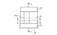
図1は、典型的なフィラメント型抵抗変化素子の動作方法の一例を示す模式図である。この抵抗変化素子は、上部電極252と抵抗変化層241と下部電極251とが積層された構成を有し、トランジスタ250に直列に接続されている。 FIG. 1 is a schematic diagram showing an example of a method for operating a typical filament variable resistance element. This resistance change element has a configuration in which an
初期化は電極間を絶縁破壊することにより行う。すなわち、(a)に示すように、上部電極252に印加する電圧VT.E.を2.5V、下部線極251に印加する電圧VB.E.を0V、トランジスタ250のゲートに印加する電圧VGを2Vに設定する。これにより、上部電極252と下部電極251との間に絶縁破壊電圧が印加される。その結果、(b)に示すように、抵抗変化層241の一部にフィラメント241aと呼ばれる低抵抗な導電性パスが、上部電極252と下部電極251との間を橋渡しするように形成される(Formingともいう)。この状態を低抵抗状態(LRS:Low Resistance State)と呼ぶ。このとき、絶縁破壊後にフィラメント241aに流れる電流を外部回路(図示されず)で制御することで、フィラメント241aが低抵抗になり過ぎないようにする。例えば、1kWの抵抗になるように流れる電流を調整する。Initialization is performed by dielectric breakdown between the electrodes. That is, as shown in (a), the voltageVT applied to the
高抵抗化はフィラメントの一部を切断することにより行う。すなわち、(b)に示すように、上部電極252に印加する電圧VT.E.を1.0V、下部線極251に印加する電圧VB.E.を0V、トランジスタ250のゲートに印加する電圧VGを5Vに設定する。その結果、(c)に示すように、フィラメント241aの一部が切断される(Resetともいう)。この状態を高抵抗状態(HRS:High Resistance state)と呼ぶ。フィラメント241aの切断は、閾値以上のパワーをフィラメント241aに投入することで発生する。このとき、フィラメント241aの両端には、閾値を越えるような電圧が印加される必要がある(P=V2/R、V>(RP)0.5)。フィラメント241aが切断された部分は、トンネル障壁モデルで説明できることがわかっている。High resistance is achieved by cutting a part of the filament. That is, as shown in (b), the voltageVT applied to the
低抵抗化は高抵抗化電圧より大きな電圧をフィラメントに印加して切断されたフィラメントを再び接続することにより行う。すなわち、(c)に示すように、上部電極252に印加する電圧VT.E.を2.5V、下部線極251に印加する電圧VB.E.を0V、トランジスタ250のゲートに印加する電圧VGを2Vに設定する。その結果、(b)に示すように、切断されたフィラメント241aが再び接続される(Setともいう)。この状態は低抵抗状態(LRS)である。フィラメント241aの再接続は、トンネル障壁の絶縁破壊をすることで発生する。Lowering the resistance is performed by applying a voltage higher than the higher resistance voltage to the filament and reconnecting the cut filament. That is, as shown in (c), the voltageVT applied to the
前述のように、抵抗変化素子の電極の材料としては、貴金属が用いられることが多い。この理由の一つとして、電極材料として貴金属を用いると、電極が酸化され難く、良好な抵抗変化特性が得られることが挙げられる。電極材料が、容易に酸化される材料であると、リテンション特性が悪化するなど、メモリセルの信頼性に悪影響を与える。 As described above, a noble metal is often used as the electrode material of the variable resistance element. One reason for this is that when a noble metal is used as the electrode material, the electrode is not easily oxidized and good resistance change characteristics can be obtained. If the electrode material is a material that is easily oxidized, the reliability of the memory cell is adversely affected, for example, the retention characteristics are deteriorated.
しかし、貴金属を用いる場合、以下のような問題点が有る。まず、貴金属をドライプロセスで加工することは困難である。加えて、貴金属はそれ自体が高価である。更に、貴金属の製造プロセスは、他の製造プロセスとの関係で、製造ラインのコンパチビリティが無いため、製造ラインの導入コストが高くなる。また、汚染の観点から、CMOSラインとの親和性も悪い。 However, when noble metals are used, there are the following problems. First, it is difficult to process a noble metal by a dry process. In addition, precious metals are themselves expensive. Furthermore, since the precious metal manufacturing process is not compatible with other manufacturing processes in relation to other manufacturing processes, the introduction cost of the manufacturing line becomes high. Further, from the viewpoint of contamination, the affinity with the CMOS line is also poor.
以上の問題点を回避するために、発明者は、抵抗変化素子の電極材料として、窒化チタンのようなラインコンパチビリティの高い既存材料を用いることを検討した。ここでは、フィラメント型の抵抗変化素子において、抵抗変化層にZrOx(酸化ジルコニウム)を用い、電極にRu(ルテニウム)又はTiNx(窒化チタン)を用いた場合について説明する。このとき、MIM(Metal/Insulator/Metal)部、すなわち、電極/抵抗変化素子/電極は、それぞれRu/ZrOx/Ru、及び、TiNx/ZrOx/TiNxである。素子サイズ及び各膜厚は、電極にRuを用いた場合とTiNxを用いた場合とで同じである。 In order to avoid the above problems, the inventor examined using an existing material having high line compatibility such as titanium nitride as the electrode material of the resistance change element. Here, the case where ZrOx (zirconium oxide) is used for the resistance change layer and Ru (ruthenium) or TiNx (titanium nitride) is used for the electrode in the filament type resistance change element will be described. At this time, the MIM (Metal / Insulator / Metal) portion, that is, the electrode / resistance change element / electrode is Ru / ZrOx / Ru and TiNx / ZrOx / TiNx, respectively. The element size and each film thickness are the same when Ru is used for the electrode and when TiNx is used.
電極にRuを用いた場合、MIM部の両端に0.5V程度の電圧を印加すると、抵抗変化素子は高抵抗化した。また、MIM部の両端に2.0V程度の電圧を印加すると、抵抗変化素子は低抵抗化した。それぞれの電圧のバラツキを考慮しても、高抵抗化電圧と低抵抗化電圧とに1.5V程度の十分なマージンがあることが分かった。したがって、電極にRuを用いた場合、高信頼な抵抗変化特性を得ることが可能である。 When Ru was used as the electrode, the resistance change element became high resistance when a voltage of about 0.5 V was applied to both ends of the MIM portion. Further, when a voltage of about 2.0 V was applied to both ends of the MIM portion, the resistance change element was reduced in resistance. It was found that there is a sufficient margin of about 1.5 V between the high resistance voltage and the low resistance voltage even when the variation of each voltage is taken into consideration. Therefore, when Ru is used for the electrode, it is possible to obtain a highly reliable resistance change characteristic.
一方、電極にTiNxを用いた場合、MIM部の両端に0.8V程度の電圧を印加しなければ、抵抗変化素子は高抵抗化しなかった。また、MIM部の両端に1.0V程度の電圧を印加すると、抵抗変化素子は低抵抗化した。それぞれの電圧バラツキを考慮すると、高抵抗化電圧と低抵抗化電圧とにほとんど電圧差が無く十分なマージンを取ることができないことが分かった。したがって、電極にTiNxを用いた場合、良好な抵抗変化特性を得ることができない。電極として貴金属を用いない場合でも、高信頼な抵抗変化素子を実現することが望まれる。比較的高い抵抗率を持つ導電体を電極に用いた場合でも、高信頼な抵抗変化素子を実現することが望まれる。他の製造プロセスとの製造ラインコパチビィティの高い材料を電極材料に用いた高信頼な抵抗変化素子を実現することが望まれる。 On the other hand, when TiNx was used for the electrode, the resistance change element did not increase in resistance unless a voltage of about 0.8 V was applied to both ends of the MIM portion. Further, when a voltage of about 1.0 V was applied to both ends of the MIM portion, the resistance change element was reduced in resistance. Considering each voltage variation, it was found that there is almost no voltage difference between the high resistance voltage and the low resistance voltage, and a sufficient margin cannot be obtained. Therefore, when TiNx is used for the electrode, good resistance change characteristics cannot be obtained. Even when noble metal is not used as an electrode, it is desired to realize a highly reliable variable resistance element. Even when a conductor having a relatively high resistivity is used for the electrode, it is desired to realize a highly reliable variable resistance element. It is desired to realize a highly reliable variable resistance element using, as an electrode material, a material having high manufacturing line compatibility with other manufacturing processes.
以下に、発明を実施するための形態で使用される番号・符号を用いて、課題を解決するための手段を説明する。これらの番号・符号は、特許請求の範囲の記載と発明を実施するための形態との対応関係を明らかにするために括弧付きで付加されたものである。ただし、それらの番号・符号を、特許請求の範囲に記載されている発明の技術的範囲の解釈に用いてはならない。 Hereinafter, means for solving the problem will be described using the numbers and symbols used in the embodiments for carrying out the invention. These numbers and symbols are added with parentheses in order to clarify the correspondence between the description of the claims and the mode for carrying out the invention. However, these numbers and symbols should not be used for interpreting the technical scope of the invention described in the claims.
本発明の不揮発性半導体記憶装置は、第1配線(54)と、第2配線(55)と、一端を第1配線(54)に、他端を第2配線(55)にそれぞれ電気的に接続されたメモリセル(70)とを具備している。メモリセル(10)は、抵抗値の変化で情報を記憶する抵抗変化層(41)と、抵抗変化層(41)の両端にそれぞれ接続され、貴金属を含まない第1電極(51)及び第2電極(52)とを備えている。第1電極(51)は、第1外側電極(43)と、第1外側電極(43)と抵抗変化層(41)との間に設けられた第1界面電極(42)とを含んでいる。第1界面電極(42)の膜厚は、第1外側電極(43)の膜厚よりも薄い。第1界面電極(42)の抵抗率は、第1外側電極(43)の抵抗率よりも高い。第1電極(51)の抵抗値(Rs)は、抵抗変化層(52)の低抵抗状態の抵抗値(Ron)よりも低い。 The nonvolatile semiconductor memory device of the present invention is electrically connected to the first wiring (54), the second wiring (55), one end to the first wiring (54), and the other end to the second wiring (55). And a connected memory cell (70). The memory cell (10) is connected to both ends of the resistance change layer (41) for storing information by a change in resistance value, and the resistance change layer (41), and includes a first electrode (51) and a second electrode that do not contain a noble metal. And an electrode (52). The first electrode (51) includes a first outer electrode (43) and a first interface electrode (42) provided between the first outer electrode (43) and the resistance change layer (41). . The film thickness of the first interface electrode (42) is thinner than the film thickness of the first outer electrode (43). The resistivity of the first interface electrode (42) is higher than the resistivity of the first outer electrode (43). The resistance value (Rs) of the first electrode (51) is lower than the resistance value (Ron) of the low resistance state of the resistance change layer (52).
本発明により、比較的高い抵抗率を持つ導電体を電極に用いた場合でも、高信頼な抵抗変化素子を実現可能となる。 According to the present invention, a highly reliable variable resistance element can be realized even when a conductor having a relatively high resistivity is used for the electrode.
以下、本発明の不揮発性半導体記憶装置及びその製造方法の実施の形態に関して、添付図面を参照して説明する。 Hereinafter, embodiments of a nonvolatile semiconductor memory device and a manufacturing method thereof according to the present invention will be described with reference to the accompanying drawings.
(第1の実施の形態)
本発明の第1の実施の形態に係る不揮発性半導体記憶装置について説明する。図2は、本発明の第1の実施の形態に係る不揮発性半導体記憶装置の抵抗変化素子の構成例を模式的に示す断面図である。抵抗変化素子40は、フィラメント型の抵抗変化素子であり、抵抗値の変化で情報を記憶する。一方の側を第1配線54に、他方の側を第2配線55にそれぞれ接続されている。第1配線54及び第2配線55は、例えばCu(銅)のようなメタル層45、49と、TaNx(窒化タンタル)のようなバリア層44、48との積層体に例示される。(First embodiment)
A nonvolatile semiconductor memory device according to a first embodiment of the present invention will be described. FIG. 2 is a cross-sectional view schematically showing a configuration example of the variable resistance element of the nonvolatile semiconductor memory device according to the first embodiment of the present invention. The
抵抗変化素子40は、抵抗値の変化で情報を記憶する。抵抗変化層41と、その両端に設けられた下部電極51及び上部電極52とを備えている。 The
下部電極51は、抵抗変化層41に電流・電圧を供給するための一方の電極である。貴金属を含まない導電性材料で形成されている。その詳細は後述される。下部電極51は、第1界面電極42と第1外側電極43とを備えている。第1界面電極42は、その一方の面を抵抗変化層41に接し、他方の面を第1外側電極43に接して形成されている。第1外側電極43は、その一方の面を第1界面電極42に接し、他方の面を第1配線54のバリア層44に接して形成されている。 The
第1界面電極42は、貴金属を含まない導電性材料であり、かつ抵抗変化層41に含まれる元素と比較して、酸化され難い材料で形成されている。例えば、第1界面電極42の材料の酸化の自由エネルギーの絶対値が抵抗変化層41に含まれる元素の酸化の自由エネルギーの絶対値よりも小さい。それにより、第1界面電極42が酸化され難くなり、良好な抵抗変化特性を得ることができ、メモリセルの信頼性が向上される。第1界面電極42の材料は、例えば、Al(アルミニウム)、Mg(マグネシウム)、W(タングステン)、Co(コバルト)、Zn(亜鉛)、Ni(ニッケル)、K(カリウム)、Li(リチウム)、Fe(鉄)、Sn(錫)、Cr(クロム)、Pb(鉛)、Ti(チタン)、Ta(タンタル)、又は、これらの合金、又は、これらの酸化物、窒化物、フッ化物、炭化物、シリサイドである。これらの材料の積層体であっても良い。このうち、上記特性の観点及び製造ラインコパチビィティの高い材料という観点から、特に、遷移金属窒化物がより好ましい。更に好ましくは、TiNx又はTaNxである。 The
第1界面電極42は、少なくとも下部電極51と抵抗変化層41との界面の酸化を防止する機能が求められているから、抵抗変化層41の表面を確実に覆うべく、2原子層程度以上であることが好ましい。一方で、上記材料は抵抗率が高い傾向にあるので、下部電極51の抵抗を低く抑えるべく、20原子層程度以下とすることが好ましい。あるいは、膜厚1nm以上、10nm程度であることが好ましい。 Since the
第1外側電極43は、貴金属を含まない導電性材料であり、かつ第1界面電極42の材料と比較して抵抗率が低い材料で形成されている。それにより、第1界面電極42が相対的に抵抗率の高い材料で形成さていても、下部電極51の全体の抵抗を下げることができる。第1外側電極43の材料は、例えば、Al(アルミニウム)、Mg(マグネシウム)、W(タングステン)、Co(コバルト)、Zn(亜鉛)、Ni(ニッケル)、K(カリウム)、Li(リチウム)、Fe(鉄)、Sn(錫)、Cr(クロム)、Pb(鉛)、Ti(チタン)、Ta(タンタル)、又は、これらの合金、又は、これらの酸化物、窒化物、フッ化物、炭化物、シリサイドである。これらの材料の積層体であっても良い。 The first
上部電極52は、抵抗変化層41に電流・電圧を供給するための他方の電極である。貴金属を含まない導電性材料で形成されている。上部電極52は、第1界面電極42及び第1外側電極43で使用可能ないずれかの材料を用いた一層の電極である。抵抗変化素子40では、少なくとも一方の電極が、上記下部電極51のような特性を有していればよいので、上部電極52は必ずしも二層構造を有している必要はない。ただし、上部電極52は、第2界面電極46と第2外側電極47とを備えていることが好ましい。第2界面電極46及び第2外側電極47は、それぞれ第1界面電極42及び第1外側電極43と同じである。その場合、酸化され難く良好な抵抗変化特性を有する低抵抗な電極とすることができる。 The
抵抗変化層41は、抵抗値の変化で情報を記憶する。抵抗変化層41の材料としては、遷移金属酸化物が例示され、好ましくはストイキオメトリックな組成(化学量論組成)のZrOx(酸化ジルコニウム)、TaOx(酸化タンタル)、又は、これらの材料の積層体が例示される。抵抗変化層41の膜厚は5nm以上、20nm程度であることが好ましい。 The
なお、本実施の形態における抵抗変化素子に含まれる構造は、隣接する層同士が、これらの少なくとも一部の領域において積層されていれば良い。 Note that in the structure included in the resistance change element in this embodiment mode, adjacent layers may be stacked in at least some of these regions.
次に、本実施の形態に係る抵抗変化素子について詳細に説明する。
本実施の形態に係る抵抗変化素子40では、初期化処理が重要となる。初期化処理は、抵抗変化層41を挟み込む下部電極51と上部電極52との間に初期化の電圧を加え、抵抗変化層41の抵抗値を電圧印加前の抵抗値よりも低くする処理であり、「Forming」と呼ばれている(非特許文献3、非特許文献4)。この処理を行った後、所定の電圧を下部電極51と上部電極52との間に印加することで、低抵抗状態から高抵抗状態、又は、高抵抗状態から低抵抗状態に抵抗変化させ、いずれかの抵抗状態を保持することができる。Next, the variable resistance element according to the present embodiment will be described in detail.
In the
本実施の形態に係る抵抗変化素子の具体例と、その比較例とについて説明する。
図3は、本発明の第1の実施の形態に係る抵抗変化素子の具体例と比較例とを模式的に示す断面図である。(a)は比較例であり、(b)は本実施の形態に係る抵抗変化素子の具体例である。A specific example of the variable resistance element according to the present embodiment and a comparative example thereof will be described.
FIG. 3 is a cross-sectional view schematically showing a specific example and a comparative example of the variable resistance element according to the first embodiment of the present invention. (A) is a comparative example, (b) is a specific example of the variable resistance element according to the present embodiment.
まず、比較例である(a)の試料の作製方法について説明する。
まず、半導体(単結晶シリコン)基板の上に、第1配線154として、膜厚50nmのCu(銅)のメタル層145及び膜厚5nmのTaNx(窒化タンタル)のバリア層144を積層する。次に、第1配線154上に、下部電極151として、膜厚5nmのTa(タンタル)の第1外側電極143及び膜厚10nmのTiNx(窒化チタン)の第1界面電極142を積層する。次に、第1界面電極142の上に、抵抗変化層141として、膜厚6nmのZrOx(酸化ジルコニウム)を形成する。次に、抵抗変化層141上に、上部電極152として、膜厚10nmのTiNx(窒化チタン)の第2界面電極146と膜厚50nmのTa(タンタル)の第2外側電極147を積層する。最後に、第2配線155として、膜厚5nmのTaNx(窒化タンタル)のバリア層148及び膜厚50nmのCu(銅)のメタル層149を積層する。各成膜方法は、DCスパッタ法、RFスパッタ法、CVD法、ALD法のいずれの方法でも良い。このようにして作製された(a)試料は、下部電極151及び上部電極152のTiNx(窒化チタン)の膜厚が相対的に厚くなっている。従って、両電極の抵抗値は相対的に高くなっている。First, a method for manufacturing a sample (a) as a comparative example will be described.
First, a 50 nm-thick Cu (copper)
次に、本実施の形態に係る抵抗変化素子の具体例である(b)の試料の作製方法について説明する。
まず、半導体(単結晶シリコン)基板の上に、第1配線54として、膜厚50nmのCu(銅)のメタル層45及び膜厚5nmのTaNx(窒化タンタル)のバリア層44を積層する。次に、第1配線54上に、下部電極51として、膜厚5nmのTa(タンタル)の第1外側電極43及び膜厚2nmのTiNx(窒化チタン)の第1界面電極42を積層する。次に、第1界面電極42の上に、抵抗変化層41として、膜厚6nmのZrOx(酸化ジルコニウム)を形成する。次に、抵抗変化層41上に、上部電極52として、膜厚2nmのTiNx(窒化チタン)の第2界面電極46と膜厚50nmのTa(タンタル)の第2外側電極47を積層する。最後に、第2配線55として、膜厚5nmのTaNx(窒化タンタル)のバリア層48及び膜厚50nmのCu(銅)のメタル層149を積層する。各成膜方法は、DCスパッタ法、RFスパッタ法、CVD法、ALD法のいずれの方法でも良い。このようにして作製された(b)試料は、下部電極51及び上部電極52のTiNx(窒化チタン)の膜厚が相対的に薄くなっている。従って、両電極の抵抗値は相対的に低くなっている。Next, a method for manufacturing a sample (b), which is a specific example of the variable resistance element according to this embodiment, will be described.
First, a 50 nm thick Cu (copper)
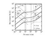
次に、上記図3の(a)試料と(b)試料の抵抗変化特性を評価した結果について説明する。図4A及び図4Bは、それぞれ図3の(a)試料及び図3の(b)試料の抵抗変化特性を示すグラフである。横軸は印加電圧、縦軸は流れる電流をそれぞれ示す。また、各グラフには複数回の抵抗変化動作が示されている。 Next, the results of evaluating the resistance change characteristics of the samples (a) and (b) in FIG. 3 will be described. 4A and 4B are graphs showing resistance change characteristics of the sample of FIG. 3A and the sample of FIG. 3B, respectively. The horizontal axis represents the applied voltage, and the vertical axis represents the flowing current. Further, each graph shows a plurality of resistance change operations.
いずれの場合にも、まず、抵抗変化層141、41の一部に導電性のフィラメントを形成するために、第1配線154、54を接地し、第2配線155、55の電圧を0Vから4Vまで挿引することで、Forming動作を行う。このとき、フィラメントの抵抗が小さくなり過ぎないように、流れる電流を300μA程度に外部の電源回路(図示されず)で電流制御する。その結果、抵抗変化素子141、41は3×10+3Ω程度の抵抗になる。In any case, first, in order to form a conductive filament in a part of the resistance change layers 141 and 41, the
高抵抗化動作は、電流制御を行わずに同様に電圧を印加することで行う。低抵抗化動作は、高抵抗化電圧以上の電圧を同様に印加することで行う。仮に、高抵抗化電圧と低抵抗化電圧が同程度の値を持つと、高抵抗状態と低抵抗状態の抵抗変化を高信頼に行うことができない。例えば、高抵抗化動作で、高抵抗化と低抵抗化が同時に発生する。 The high resistance operation is performed by applying a voltage in the same manner without performing current control. The low resistance operation is performed by similarly applying a voltage higher than the high resistance voltage. If the high resistance voltage and the low resistance voltage have similar values, the resistance change between the high resistance state and the low resistance state cannot be performed with high reliability. For example, in the high resistance operation, the high resistance and the low resistance occur simultaneously.
図4Aに示すように、図3の(a)試料の抵抗変化動作では、0.8V近傍で高抵抗化が、1.1V近傍で低抵抗化がそれぞれ発生していることがわかる。高抵抗化と低抵抗化との電圧マージンは、僅か0.3V程度である。そのため、電圧バラツキが存在することを考慮すると、抵抗変化動作を高い信頼性で行うことは非常に困難である。 As shown in FIG. 4A, it can be seen that in the resistance changing operation of the sample in FIG. 3A, a high resistance occurs near 0.8 V and a low resistance occurs near 1.1 V. The voltage margin between high resistance and low resistance is only about 0.3V. Therefore, it is very difficult to perform the resistance change operation with high reliability in consideration of the existence of voltage variation.
一方、図4Bに示すように、図3の(b)試料の抵抗変化動作では、0.5V近傍で高抵抗化が、1.5V近傍で低抵抗化がそれぞれ発生していることがわかる。高抵抗化と低抵抗化との電圧マージンは、1.0V程度である。そのため、電圧バラツキが存在することを考慮しても、抵抗変化動作を高い信頼性で行うことが可能である。 On the other hand, as shown in FIG. 4B, it can be seen that, in the resistance changing operation of the sample in FIG. 3B, a high resistance is generated in the vicinity of 0.5V and a low resistance is generated in the vicinity of 1.5V. The voltage margin between high resistance and low resistance is about 1.0V. Therefore, it is possible to perform the resistance change operation with high reliability even in consideration of the existence of voltage variation.
以上のように、(a)試料と(b)試料とでは、その抵抗変化特性が大きく異なることが分かる。両試料の相違点は、既述のように、下部電極及び上部電極のTiNx(窒化チタン)の膜厚、すなわち、下部電極及び上部電極の抵抗値である。膜厚が相対的に薄く抵抗値が低い(b)試料の方が、良好な抵抗変化特性を有することが分かる。以下では、その理由(メカニズム)について説明する。 As described above, it can be seen that the resistance change characteristics are greatly different between the sample (a) and the sample (b). As described above, the difference between the two samples is the film thickness of TiNx (titanium nitride) of the lower electrode and the upper electrode, that is, the resistance value of the lower electrode and the upper electrode. It can be seen that the sample having a relatively thin film thickness and a low resistance value (b) has better resistance change characteristics. The reason (mechanism) will be described below.
図5A〜図5Dは、電極の抵抗と抵抗変化動作との関係を説明するための模式図である。図5Aは抵抗変化素子における低抵抗状態の側面図であり、図5Bは図5Aの抵抗変化素子におけるQ−Q*断面図である。図5C及び図5Dは図5Aの抵抗変化素子の等価回路である。5A to 5D are schematic diagrams for explaining the relationship between the resistance of the electrode and the resistance changing operation. 5A is a side view of the variable resistance element in a low resistance state, and FIG. 5B is a QQ* cross-sectional view of the variable resistance element of FIG. 5A. 5C and 5D are equivalent circuits of the variable resistance element of FIG. 5A.
図5A及び図5Bに示すように、抵抗変化素子は、初期化動作により形成されたフィラメント41aを有する抵抗変化層41と、その上下に設けられた上部電極52及び下部電極51とを備えている。ここでは、抵抗変化層41の直径をF、フィラメント41aの直径をdとする。また、上部電極52及び下部電極51を区別する必要が無い場合、いずれか一方の電極を単に電極部58ともいう。 As shown in FIGS. 5A and 5B, the resistance change element includes a
低抵抗状態にある抵抗変化素子40のMIM部(上部電極52/抵抗変化層41/下部電極51)の抵抗RMINは、フィラメント41aの抵抗RFilamentに加えて、それに接続された上部電極52の抵抗RsT.E.及び下部電極51の抵抗RsB.E.も考慮する必要がある(図5C)。すなわち、
RMIN=RFilament+RsT.E.+RsB.E. … (0)
である。このとき、上部電極52及び下部電極51の抵抗RsT.E.及びRsB.E.がフィラメント41aの抵抗RFilamentと比較して無視できない場合、フィラメント41aに印加される実効的な電位差は、MIM部に印加される電圧と比較して、無視できない程度に小さくなっている。The resistance RMIN of the MIM portion (
RMIN = RFilament + RsT.R. E. + RsB.B. E. ... (0)
It is. At this time, the resistance RsT. of the
このとき、各電極の抵抗RsT.E.及びRsB.E.とフィラメントの抵抗RFilamentとの関係は以下のように考えられる。
式(1)に示されるように、フィラメント41aに印加される電圧VFilamentは、各電極部58で電圧降下が生じるために、上部電極52と下部電極51との間に印加される電圧VMINより小さくなる。したがって、式(2)に示されるように、フィラメント41aに高抵抗化するための十分な電圧を印加するためには、各電極部58での電圧降下を考慮して、より大きな電圧を印加する必要がある。仮に、式(3)(図5D)で示されるように電極部58の抵抗をRsとし、式(4)で示されるように高抵抗化させるためにフィラメント41aに印加しなければならない電圧をVRESETとする。そうすると、高抵抗化動作時に上部電極52と下部電極51との間に印加しなければならない電圧VMINは、式(2)〜式(4)より、式(5)のようになる。当然、その高抵抗化動作に必要な電圧VMIN(式(5))は、式(6)に示すように、低抵抗化電圧VSETよりも小さくなければならない。結果として、電極部58の抵抗Rsとフィラメント41aの抵抗RFilamentとの関係は、式(7)を満たさなければならない。式(7)を変形すれば、式(8)を満たさなければならない。例えば、高抵抗化させるためにフィラメント41aに印加しなければならない電圧VRESETが0.5V、低抵抗化させるためにフィラメント41aに印加しなければならない電圧VSETが1.5Vの場合、式(8)より、Rs<RFilamentとなる。従って、電極部58の抵抗Rsがフィラメント41aの抵抗RFilamentより小さくなければ抵抗変化を制御することができない。すなわち、抵抗変化動作の制御性を向上させるためには、電極部58の抵抗Rsをフィラメント41aの抵抗RFilamentよりも十分に小さくする必要がある。As shown in the equation (1), the voltage VFilament applied to the
ここで、電極部58の抵抗Rsについて更に検討する。図6は、電極部及びその周辺を示す模式図である。図6に示されるように、円盤状の電極部58が円柱状の導電性フィラメント41aに接していると仮定する。また、フィラメント41aの直径をd、長さをl、電極部58の直径をF、厚さをhとそれぞれ定義する。
フィラメント41aに接した電極部58の抵抗Rsは、式(9)に示されるように、電極部58のバルク抵抗RBulk、広がり抵抗RSp、接触抵抗RCOの3つの成分に分けて定義できる。バルク抵抗RBulkは、電極部58の材料そのものの抵抗である。広がり抵抗RSpは、フィラメント41aから電極部58へ電流が流れ込むとき、フィラメント41a(断面積小)から電極部58(断面積大)の全面へ電流が広がるときの抵抗、又はその逆の場合の抵抗である。接触抵抗RCOは、フィラメント41aと電極部58との間の接触抵抗である。The resistance Rs of the
電極部58のバルク抵抗RBulkは、内部に組成プロファイルがない場合、式(10)に示されるように、オームの法則で書き表される。ただし、電極部58の抵抗率をρ、電極部58の断面積をA(=πF2/4)とする。広がり抵抗RSpは、式(11)に示されるように、電極部58の厚さhと抵抗率ρ、フィラメント41aの直径dに依存する。接触抵抗RCOは、電極部58とフィラメント41aの界面のショットキー障壁が主要因であると考えられ、式(12)のように書き表すことができる。しかし、実際の計測結果では低抵抗状態の電流電圧特性がオーミックであることから、接触抵抗の効果は無視できるほど小さいと推察される(RCO≒0)。したがって、電極部58の抵抗Rsは、式(13)のようにモデル化される。The bulk resistance RBulk of the
ここで、広がり抵抗RSp(式(14);式(11)の再掲)は、電極部58の厚さhとフィラメント41aの直径dとの関係で値が異なってくる。
電極部58の厚さhがフィラメント41aの直径dより十分に大きい場合、式(14)は式(15)のように書き表される。すなわち、広がり抵抗RSpは、フィラメント41aの直径dと電極部58の抵抗率ρにのみ依存した量になる。一方、電極部58の厚さhがフィラメント41aの直径dより十分に小さい場合、式(14)は、フィラメント41aの断面積をSとして、式(16)のように書き表される。すなわち、広がり抵抗RSpは、フィラメント41aの断面積Sと電極部58の抵抗率ρ及び厚さhに依存した量になる。When the thickness h of the
次に、式(14)〜式(16)を考慮しつつ、式(13)の電極部58の抵抗Rsを計算した結果について説明する。図7は、電極部58の抵抗Rsを計算した結果を示すグラフである。横軸は電極部58の厚さh、縦軸は電極部58の抵抗Rsである。曲線A1、A2、A3は、それぞれフィラメント41aの直径dが1nm、10nm、100nmの場合での電極部58の抵抗Rs(式(13))の厚さh依存性を示している。このとき、電極部58の直径Fは100nm、抵抗率ρは300μΩcm(TiNx相当)と仮定している。 Next, the result of calculating the resistance Rs of the
例えば、フィラメント41aの直径dが10nmの場合(曲線A2)、電極部58の厚さhが1μm(1×10³nm)以下の領域において、電極部58のバルク抵抗RBulkより広がり抵抗RSpのほうが十分に大きくなる。したがって、フィラメント41aの直径dより電極部58の厚さhが大きい領域、つまり10(1×101)nmから1μm(1×10³nm)までの間で、電極部58の抵抗Rsは大きく変化しない。一方、電極部58の厚さhが10(1×101)nmより小さい場合、電極部58の抵抗Rsは電極部58の厚さhに比例して減少する。特に、電極部58の厚さhがフィラメント41aの直径dの60%程度(曲線A2ではh=6nm程度)以下の場合、電極部58の厚みhの減少に伴い抵抗Rsが顕著に減少している。なお、破線αIは、電極部58の抵抗Rsが電極部58の厚さhに比例して減少し始める点を示している。フィラメント41aの直径dが1、10、100nmの場合、それぞれの電極部58の厚さhがフィラメント41aの直径dの70%、60%、40%となる点となる。フィラメント41aの直径dは少なくとも100nm以下であるから、電極部58の厚みhを少なくとも80%以下とすることで、抵抗値が急激に減少し始める。For example, when the diameter d of the
図8は、電極部58の抵抗Rsを計算した結果を示すグラフである。横軸は電極部58の厚さh、縦軸は電極部58の抵抗Rsである。曲線B1、B2、B3は、それぞれ電極部58の低効率ρが300μΩcm(TiNx相当)、15μΩcm(Ru相当)、1.7μΩcm(Cu相当)の場合での電極部58の抵抗Rs(式(13))の厚さh依存性を示している。このとき、電極部58の直径Fは100nm、フィラメント41aの直径dは10nmと仮定している。 FIG. 8 is a graph showing the result of calculating the resistance Rs of the
電極部58の材料の抵抗率ρを変えた場合、抵抗率ρが小さいほうが、電極部58の抵抗Rsは小さい。なお、破線αI、αII、αIIIは、電極部58の抵抗Rsが電極部58の厚さhに比例して減少し始める点を示している。When the resistivity ρ of the material of the
以上のことから、膜厚が相対的に薄く抵抗値が低い(b)試料のような結果を得るためには、フィラメント41aの直径dが同じ場合、つまり、低抵抗状態の抵抗値が同じ場合、抵抗率ρの小さな電極材料を選択することが好ましい。また、電極部58の厚さhをフィラメント41aの直径の80%以下にすることが好ましい。それにより、抵抗変化の制御性が向上し、結果的に、信頼性の高い抵抗変化素子が実現される。なお、ここでの抵抗率ρは、電極部58全体での抵抗率である。したがって、上記図2や図3の(b)試料の抵抗変化素子40の場合、下部電極51で言えば、下部電極51を構成する第1界面電極42と第1外側電極43の平均抵抗率ということができる。上部電極52で言えば、上部電極52を構成する第2界面電極46と第2外側電極47の平均抵抗率ということができる。 From the above, in order to obtain a result like a sample having a relatively thin film thickness and a low resistance value, the diameter d of the
本実施の形態の抵抗変化素子では、少なくとも下部電極51及び上部電極52のうちの少なくとも一方の電極を二層構造とし、抵抗変化素子との界面側の界面電極を酸化し難い電極とし、その外側の外側電極を低抵抗な電極としている。それにより、その電極での抵抗を抵抗変化素子(フィラメント)での抵抗よりも十分に小さくすることができる。その結果、抵抗変化動作の制御性を向上させることができる。 In the resistance change element according to the present embodiment, at least one of the
(第2の実施の形態)
本発明の第2の実施の形態に係る不揮発性半導体記憶装置について説明する。図9は、本発明の第2の実施の形態に係る不揮発性半導体記憶装置の抵抗変化素子の構成例を模式的に示す断面図である。本実施の形態に係る抵抗変化素子40aは、第1の実施の形態の抵抗変化素子40と比較すると、下部電極51a及び上部電極52aの構成が第1の実施の形態の下部電極51及び上部電極52と相違している。以下では、相違点について主に説明する。(Second Embodiment)
A nonvolatile semiconductor memory device according to the second embodiment of the present invention will be described. FIG. 9 is a cross-sectional view schematically showing a configuration example of the variable resistance element of the nonvolatile semiconductor memory device according to the second embodiment of the present invention. The
抗変化素子40aは、抵抗値の変化で情報を記憶する。抵抗変化層41と、その両端に設けられた下部電極51a及び上部電極52aとを備えている。 The
下部電極51aは、貴金属を含まない導電性材料で形成されているが、その内部に低効率傾斜を有している。すなわち、抵抗変化層41側の抵抗率が高く、第1配線54側の抵抗率が低くなるように設けられている。途中は、抵抗変化層41側から第1配線54側に向かって、抵抗率が高い値から低い値に遷移している。例えば、抵抗変化層41側が金属の窒化物であり、第1配線54側がその金属単体である。途中は、抵抗変化層41側から第1配線54側に向かって、金属中の窒素が高濃度から低濃度に遷移している。一例としては、抵抗変化層41側がTiNxであり、第1配線54側がTiである。途中は、抵抗変化層41側から第1配線54側に向かって、Ti1−XNXのXが0.5から0に遷移している。遷移の仕方は、連続的に変化しても良いし、複数のステップ状に変化しても良い。The
このとき、金属の窒化物は、抵抗変化層41に含まれる元素と比較して、相対的に抵抗率は高いが酸化され難い材料である。すなわち、下部電極51aのうちの抵抗変化層41に接する側は、第1の実施の形態における第1界面電極(42)とみることができる。一方、金属単体は、その金属の窒化物と比較して、相対的に抵抗率が低い材料である。すなわち、下部電極51aのうち第1配線54に接する側は、第1の実施の形態における第1外側電極(43)とみることができる。従って、下部電極51aは、第1界面電極(42)及び第1外側電極(43)で構成された、抵抗率傾斜を有する疑似的な二層構造とみることもできる。ただし、この場合、第1界面電極(42)及び第1外側電極(43)は、いずれも膜中の組成が均一でなく段階的に変化している。 At this time, the metal nitride is a material that has a relatively high resistivity but is not easily oxidized as compared with the element included in the
下部電極51aの材料は、第1の実施の形態に既述したように、貴金属を含まない導電性材料であり、かつ抵抗変化層41に含まれる元素と比較して酸化され難い材料である。第1の実施の形態に既述した材料を用いることができる。ただし、本実施の形態では、金属とその窒化物、酸化物、炭化物を用いる。
特に、遷移金属とその窒化物を用いることが好ましい。例えば、TiとTiNx、TaとTaNx、WとWNxなどである。As described in the first embodiment, the material of the
In particular, it is preferable to use a transition metal and its nitride. For example, Ti and TiNx, Ta and TaNx, W and WNx, and the like.
下部電極51aの製造は、例えば、下部電極51aに用いる金属膜のうちの抵抗変化層41に接する側を窒化する方法が考えられる。第1の実施の形態に既述したように、第1界面電極(42)は薄くても良いからである。あるいは、下部電極51aに用いる金属膜をスパッタ法などにより成膜しつつ、抵抗変化層41に接する側に近づくに連れて窒素ガスを導入し、増加させて金属の窒化物膜とする方法が考えられる。 For manufacturing the
その他については、第1の実施の形態の第1界面電極42及び第1外側電極43と同様である。 Others are the same as those of the
上部電極52aは、第1の実施の形態と同じであっても良いし、好ましくは下部電極51aと同じ構成を有していてもよい。下部電極51aと同じ構成とする場合、下部電極51aに用いる金属の窒化物膜を、窒素ガスを用いたスパッタ法などにより成膜しつつ、抵抗変化層41に接する側から遠ざかるに連れて窒素ガスを減少させ、最終的に停止して金属膜とする方法が考えられる。 The
この場合にも、第1の実施の形態と同様の効果を得ることができる。
また、各電極として、二つの層を積層しなくて良いので、製造プロセスが容易化される。In this case, the same effect as that of the first embodiment can be obtained.
Moreover, since it is not necessary to laminate | stack two layers as each electrode, a manufacturing process is facilitated.
(第3の実施の形態)
本発明の第3の実施の形態に係る不揮発性半導体記憶装置について説明する。図10は、本発明の第3の実施の形態に係る不揮発性半導体記憶装置の構成例を示す断面図である。本実施の形態に係る不揮発性半導体記憶装置1は、第1の実施の形態の抵抗変化素子40(又は第2の実施の形態の抵抗変化素子40a)を含んだメモリセル70を備えている。なお、この図において、電流・電圧の供給・印加を行う回路の記載を省略している(以下同じ)。(Third embodiment)
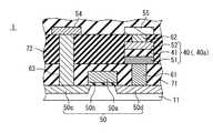
A nonvolatile semiconductor memory device according to the third embodiment of the present invention will be described. FIG. 10 is a cross-sectional view showing a configuration example of the nonvolatile semiconductor memory device according to the third embodiment of the present invention. The nonvolatile
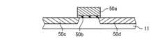
不揮発性半導体記憶装置1は、複数の第1配線54と、複数の第2配線55と、複数の第3配線(図示されず)と、複数のメモリセル70とを具備している。ただし、この図においては、一つのメモリセル70及びその周辺部を示しているため、第1配線54、第2配線55及びメモリセル70は、それぞれ一つ示している。 The nonvolatile
複数の第1配線54は、ビット線となる配線であり、例えば互いに平行にX方向に延在している。複数の第2配線55は、接地されている配線であり、例えば互いに平行にX方向に延在している。複数の第3配線(図示されず)は、ワード線になる配線であり、例えば互いに平行にY方向に延在している。複数のメモリセル70は、複数の第1配線54と複数の第3配線(図示されず)との交点の各々に対応して設けられている。メモリセル70は、トランジスタ50と、抵抗変化素子40(又は40a)とを備えている。 The plurality of
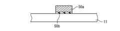
トランジスタ50は、制御トランジスタであり、MOSトランジスタに例示される。p型の単結晶シリコンからなる半導体基板11の表面領域に設けられている。ゲート50aとゲート絶縁層50bとソース50cとドレイン50dとを備えている。トランジスタ50上には、それを覆うように層間絶縁層71が設けられている。 The
抵抗変化素子40(又は40a)は、層間絶縁層71上に設けられている。下部電極51、抵抗変化層41及び上部電極52を備え、第1の実施の形態(又は第2の実施の形態)に記載のとおりである。例えば、下部電極51及び上部電極52はTiNxとWの積層構造である。例えば、抵抗変化層41はZrOxである。下部電極51は、層間絶縁膜71を貫通するコンタクトビア61により、ドレイン50dに接続されている。抵抗変化素子40及び層間絶縁層71上には、それらを覆うように層間絶縁膜72が設けられている。 The resistance change element 40 (or 40a) is provided on the
第1配線54は、層間絶縁層71、72を貫通するコンタクトビア63により、ソース50cに接続されている。第2配線55は、層間絶縁層72に設けられたビア62により、上部電極52に接続されている。第3配線(図示されず)は、メモリセル70の近傍でゲート50aに接続されている。 The
なお、上述した制御トランジスタ(トランジスタ50)は、n型電界効果トランジスタ(nFET)である。ただし、p型電界効果トランジスタ(pFET)であっても良い。ゲート絶縁層50bは、例えば、SiO2(酸化シリコン)から構成すればよい。例えば、半導体基板11の表面を熱酸化することで形成できる。ただし、HfOx(酸化ハフニウム)、ZrOx(酸化ジルコニウム)、及びAlOx(酸化アルミニウム)などの金属酸化物から構成してもよい。また、シリケートや窒化物であってもよく、これらの積層構造であっても良い。The control transistor (transistor 50) described above is an n-type field effect transistor (nFET). However, it may be a p-type field effect transistor (pFET). The
ゲート50aは、例えば、リンが添加されたポリシリコンで構成することができる。ただし、メタルゲートやシリサイドゲートであってもよい。下部電極51及び上部電極52は、例えば、膜厚2nmのTiNxと膜厚5nmのWの積層構造で構成することができる。ただし、前述したように、各電極は、第1の実施の形態において記述された材料を用いることもできる。また、抵抗変化層41は、層厚10nmのZrOxで構成することができる。ただし、第1の実施の形態において記述された材料を用いることもできる。 The
次に、図10に記載の不揮発性半導体記憶装置1の動作方法(抵抗変化素子40、40aの動作方法)について説明する。まず、「Forming」を行うため、例えば、ゲート50aに正の電圧を印加してトランジスタ50をオンの状態とし、第1配線54に正の電圧を印加して下部電極51に正の電圧を印加し、抵抗変化層41を低抵抗化する。このとき、ゲート50aに印加する電圧を調整して、トランジスタ50により電流制限がかかるようにし、抵抗変化層41が所望の抵抗値になるようにする。なお、「Forming」は、第1配線54の替わりに第2配線55に電圧を印加してもよい。 Next, an operation method of the nonvolatile
「Forming」後に低抵抗状態と高抵抗状態とを切り替えるときにも、トランジスタ50がオンの状態で、第1配線54に所定の電圧の正の電圧を印加する。低抵抗状態から高抵抗状態に抵抗変化をさせるときには、第1配線54に、低抵抗状態への抵抗変化をさせるときよりも低い電圧を印加する。ゲート50aに印加する電圧を調整し、トランジスタ50による電流制限がかからないようにする。一方、高抵抗状態から低抵抗状態に抵抗変化をさせるときには、第1配線54に、高抵抗状態への抵抗変化をさせるときよりも高い電圧を印加する。そのとき、ゲート50aに印加する電圧を調整し、トランジスタ50による電流制限がかかるようにし、抵抗変化層41が所望(所定)の抵抗値になるようにする。なお高抵抗状態から低抵抗状態へ抵抗変化をさせるときには、第1配線54の替わりに第2配線55に正の電圧を印加しても良い。 Even when the low resistance state and the high resistance state are switched after “Forming”, a positive voltage of a predetermined voltage is applied to the
次に、不揮発性半導体記憶装置1の製造方法について説明する。図11A〜図11Fは、本発明の第3の実施の形態に係る不揮発性半導体記憶装置の製造方法を示す断面図である。 Next, a method for manufacturing the nonvolatile
まず、図11Aに示すように、半導体基板11の上にゲート絶縁層50b及びゲート50aを形成する。例えば、SiO2(酸化シリコン)膜及びp−doped poly−Si(リン添加ポリシリコン)膜を堆積し、これらの膜を公知のフォトリソグラフィ技術及びエッチング技術を用いてパターニングする。それにより、ゲート絶縁層50b及びゲート50aを形成する。First, as illustrated in FIG. 11A, the
次に、図11Bに示すように、ゲート50aをマスクとし、2×1015cm−2(設定値)でP(リン)をイオン注入することで、ソース50c及びドレイン50bを形成する。Next, as shown in FIG. 11B, the
次に、図11Cに示すように、半導体基板11の全面にSiO2(酸化シリコン)を堆積し、この堆積膜の表面をCMP(Chemical Mechanical Polishing)法により平坦化して層間絶縁層71を形成する。次に、層間絶縁層71に、公知のフォトリソグラフィ技術及びエッチング技術を用いてドレイン50dに到達するコンタクトホールを形成する。続いて、TiNx(窒化チタン)及びW(タングステン)を積層してコンタクトホール内を充填する。その後、CMP法を用いて層間絶縁層71上の積層膜を除去し、コンタクトビア61を形成する。Next, as shown in FIG. 11C, SiO2 (silicon oxide) is deposited on the entire surface of the
次に、図11Dに示すように、コンタクトビア61を形成した層間絶縁層71上にW(タングステン)層を5nm、TiNx(窒化チタン)層を5nm、ZrOx(酸化ジルコニウム)層を10nm、TiNx(窒化チタン)層を5nm及びW(タングステン)層を5nmを順次堆積し、これらを公知のフォトリソグラフィ技術及びエッチング技術によりパターニングする。それにより、下部電極51、抵抗変化層41、及び上部電極52より構成された抵抗変化素子40を形成する。 Next, as shown in FIG. 11D, the W (tungsten) layer is 5 nm, the TiNx (titanium nitride) layer is 5 nm, the ZrOx (zirconium oxide) layer is 10 nm, and the TiNx (TiNx) layer is formed on the
次に、図11Eに示すように、抵抗変化素子40及び層間絶縁層71を覆うように、SiO2(酸化シリコン)を堆積し、この堆積膜の表面をCMP法により平坦化して層間絶縁層72を形成する。Next, as shown in FIG. 11E, SiO2 (silicon oxide) is deposited so as to cover the
次に、図11Fに示すように、公知のフォトリソグラフィ技術及びエッチング技術を用いたパターニングにより、層間絶縁層72及び層間絶縁層71に、ソース50cに到達する貫通孔および上部電極52に到達する貫通孔を形成する。次いで、TiN(窒化チタン)及びW(タングステン)を堆積し、これらで貫通孔内を充填する。この後、CMP法を用いて表面を平坦化するとともに、貫通孔以外の窒化チタンおよびタングステンを除去する。それにより、コンタクトビア63およびビア62を形成する。その後、層間絶縁層72の上にTiNx(窒化チタン)及びAl(アルミニウム)を堆積し、これら堆積膜を公知のフォトリソグラフィ技術及びエッチング技術によりパターニングすることで、第1配線54及び第2配線55を形成する。 Next, as shown in FIG. 11F, through-holes reaching the
上述したように製造された不揮発性半導体記憶装置1では、上記第1の実施の形態(又は第2の実施の形態)に係る抵抗変化素子40(又は40a)を、トランジスタ50のドレイン50dに接続して構成している。そのためメモリセル70の占める面積がトランジスタ50の占める面積のみとなるので、高集積化に有利である。また、不揮発性半導体記憶装置1では、初期リークが小さく、安定した抵抗変化動作を実現可能という本発明の特徴に加えて、「Forming」のための電圧印加時や高抵抗から低抵抗への抵抗変化時に、トランジスタ50のゲート電圧によって電流制御できるため、低バラツキの抵抗変化動作を実現できる。 In the nonvolatile
(第4の実施の形態)
本発明の第4の実施の形態に係る不揮発性半導体記憶装置について説明する。図12は、本発明の第4の実施の形態に係る不揮発性半導体記憶装置の構成例を模式的に示す斜視図である。不揮発性半導体記憶装置1Aは、抵抗変化型不揮発メモリ(ReRAM)であり、複数のビット線13と、複数のワード線20と、複数のメモリセル10とを具備している。なお、この図において、電流・電圧の供給・印加を行う回路の記載を省略している。(Fourth embodiment)
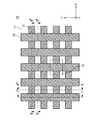
A nonvolatile semiconductor memory device according to the fourth embodiment of the present invention will be described. FIG. 12 is a perspective view schematically showing a configuration example of the nonvolatile semiconductor memory device according to the fourth embodiment of the present invention. The nonvolatile
複数のビット線13は、互いに平行にX方向に延在している。複数のビット線13は、基板11に埋設されている。複数のワード線20は、互いに平行に、X方向とは垂直なY方向に延在している。ビット線13及びワード線20は、例えば、それぞれ第1、2の実施の形態における第1配線54及び第2配線55である。複数のメモリセル10は、複数のビット線13と複数のワード線20との交点の各々に設けられている。メモリセル10は、一端をビット線13に他端をワード線20にそれぞれ接続されている。メモリセル10は、直列接続されたダイオード15と抵抗変化部19とを備えている。すなわち、1D1R構造である。 The plurality of
ダイオード15は、整流機能を有する。ビット線13上に設けられている。第1半導体層13と第2半導体層14とを含んでいる。第1半導体層13は、ビット線13に接して形成されている。第2半導体層14は、第1半導体層13の内部に埋設され、抵抗変化部19に接して形成されている。第1半導体層13及び第2半導体層14のうちの一方がアノードであり、他方がカソードである。 The
抵抗変化部19は、抵抗値の変化で情報を記憶する。ダイオード15の上方に設けられている。抵抗変化部19は、第1、2の実施の形態における抵抗変化素子40、40aである。上部電極18と下部電極16と抵抗変化層17とを含んでいる。上部電極18は、ワード線20に接続されている。下部電極16は、ダイオード15に接続されている。抵抗変化層17は、上部電極18と下部電極16との間に設けられ、両電極に印加される電圧(電流)により、抵抗値を変化させる。下部電極16と抵抗変化層17と上部電極18とワード線20とは、この順に積層されている。 The
上部電極18、下部電極16及び抵抗変化層17は、それぞれ第1の実施の形態における上部電極52、下部電極51及び抵抗変化層41であるか、又は、それぞれ第2の実施の形態における上部電極52a、下部電極51a及び抵抗変化層41である。すなわち、上部電極18及び下部電極16の少なくとも一方は、第1の実施の形態のように界面電極と外側電極の二層構造を有しているか、又は、第2の実施の形態のように抵抗率傾斜を有する疑似的な二層構造を有している。 The
次に、不揮発性半導体記憶装置1Aの詳細について説明する。
図13Aは、本発明の第4の実施の形態に係る不揮発性半導体記憶装置の構成例(図12)の平面図である。メモリセル10は、破線で示す領域である。この領域のX方向及びY方向の幅は、ワード線20及びビット線13の幅をいずれも最小加工寸法Fとすれば、いずれも2Fである。すなわち、メモリセル10の面積は、(2F)2=4F2であり、最小単位セル面積である。このように、このメモリセル10は、1D1R構造を有し、最小単位セル面積を可能にしている。Next, details of the nonvolatile
FIG. 13A is a plan view of a configuration example (FIG. 12) of the nonvolatile semiconductor memory device according to the fourth embodiment of the present invention. The
図13B〜図13Eは、それぞれ図13AにおけるI−I*断面図、II−II*断面図、III−III*断面図、及びIV−IV*断面図である。ただし、I−I*断面はワード線20を含むyz断面である。II−II*断面は、ワード線20を含まないyz断面である。III−III*断面はビット線13を含むxz断面である。IV−IV*断面はビット線13を含まないxz断面である。Figure 13B~ FIG. 13E, II* cross-sectional view respectively, in FIG 13A, II-II* cross-sectional view, III-III* sectional view, and a IV-IV* cross section. However, the II* section is a yz section including the
基板11は、第2導電型の半導体基板であり、p型Si(シリコン)基板に例示される。基板11は、複数の素子分離絶縁層12(Shallow Trench Insulator;STI)を備えている。複数の素子分離絶縁層12は、互いに平行にX方向に延在している。ただし、素子分離絶縁層12の底面(−z側の面)は平坦である。一方、素子分離絶縁層12の上面(+z側の面)は、ワード線20の直下(図13B)以外の部分では、上部が部分的に除去されて薄くなっている(図13C)。すなわち、素子分離絶縁層12は、ワード線20の配置の周期に対応して、膜厚が薄い部分と厚い部分とが交互に現れる(図13E)。素子分離絶縁層は、SiO2(酸化シリコン)に例示される。Y方向では、複数のビット線13は、複数の素子分離絶縁層12により分離されている。The
複数のビット線13は、基板11に接して形成されている。ビット線13の底面(−z側の面)は平坦である。一方、ビット線13の上面(+z側の面)は、メモリセル10が無い部分では、基板11の上面(素子分離絶縁層12の表面)と同じ面にある(図13C)。しかし、メモリセル10が有る部分では、ダイオード15(の第2半導体層14)の分だけ凹んでいる(薄くなっている;図13B)。すなわち、ビット線13は、メモリセル10の配置の周期に対応して、膜厚が薄い部分と厚い部分とが交互に現れる(図13D)。ビット線13は、基板11と異なる第1導電型の半導体の配線であり、n+型Si(シリコン)の配線に例示される。高濃度ドープ半導体(例示:n+型シリコン)を用いることで、ビット線13の抵抗を低減することができる。ビット線13の膜厚方向の第1導電型濃度は、必ずしも均一である必要はなく、所定の濃度範囲に入っていればよい。 The plurality of
ダイオード15の第1半導体層13は、ビット線13に含まれ、ビット線13におけるメモリセル10のある領域である(図13D)。第1半導体層13は、その領域のビット線13の少なくとも上部と実質的に同一である。すなわち、ビット線13(少なくともその上部)は、その領域において、第1半導体層13を兼ねている。第1半導体層13は、ビット線13と同じく、第1導電型であり、n+型Si(シリコン)に例示される。第1半導体層13の膜厚方向の第1導電型濃度は、必ずしも均一である必要はなく、所定の濃度範囲に入っていればよい。 The
ダイオード15の第2半導体層14は、ビット線13(第1半導体層13)の上部からその内部の途中まで伸びている(図13D)。第2半導体層14は、ビット線13(第1半導体層13)の凹部(又は窪み)に埋設されていると見ることもできる。すなわち、凹型形状を有する(又は窪みを有する)第1半導体層13の凹部(又は窪み)を埋めるように第2半導体層14が形成されている(図13D)。なお、図13Dの例では、第1半導体層13の凹部(又は第2半導体層14)の形状は、概ね直方体形状であるが、本実施の形態はこの例に限定されるものではない。すなわち、凹部(又は第2半導体層14)の形状は、第1半導体層13との接触面積(接合面積)を増加させるような他の形状を有していても良いし、その数は複数あっても良い。第2半導体層14は、それらの凹部(又は窪み)を埋めるように形成される。第2半導体層14は、第1導電型と異なる第2導電型であり、p+型Si(シリコン)に例示される。第1導電型濃度及び第2半導体層14の膜厚方向の第2導電型濃度は、必ずしも均一である必要はなく、所定の濃度範囲に入っていればよい。 The
第1半導体層13や第2半導体層14は、後述されるように基板11の半導体をそのまま利用して製造されることが好ましい。多結晶シリコンや選択エピタキシャル成長のシリコンの場合、既述のように、ダイオード15に流せる電流が制限されるおそれがあるからである。 The
ダイオード15がこのような構成を有することにより、第2半導体層14は、その−Z方向の底面だけでなく、そのX方向の両側面においても第1半導体層13と接触することができる。従って、第1半導体層と第2半導体層とを単純に積層して平面で接触させている場合と比較して、第1半導体層13と第2半導体層14との接触面積を大きくすることができる。この接触面積は、ダイオード15における接合面積に対応する。したがって、上記構成により、ダイオード15の接合面積を増加させ得ることができ、ダイオード15に流すことが出来る電流を増加させることが可能となる。 Since the
抵抗変化部19の下部電極16は、メモリセル10が有る部分において、基板11の上面(素子分離絶縁層12の表面)と同じ面にある(図13B)。抵抗変化層17と上部電極18とは、この順に積層されて、Y方向に延在している(図13B)。抵抗変化層17は、例えば膜厚10nm程度である。上部電極18及び下部電極16は、例えば膜厚20nm程度である。 The
ワード線20は、抵抗変化層17及び上部電極18の上に積層されて、Y方向に延在している(図13B)。 The
ワード線20、ビット線13及びメモリセル10を覆うように、層間絶縁層21が形成されている。層間絶縁層21の上部は平坦化されている。 An interlayer insulating
上記構成を有することにより、本実施の形態に係る不揮発性半導体記憶装置1Aでは、メモリセル10が1D1R構造を有し、最小単位セル面積4F2で構成することができる。その結果、高集積化を図ることができる。また、埋め込みビット線13は高濃度ドープ半導体を用いているので、その抵抗を低減することができる。その結果、動作速度を向上させることができる。また、第1半導体層13と第2半導体層14との接触面積を大きくすることができる。その結果、ダイオード15の接合面積を増加させ得ることができ、ダイオード15に流すことが出来る電流を増加させることが可能となる。By the above configuration, in the non-volatile
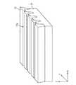
次に、本発明の第4の実施の形態に係る不揮発性半導体記憶装置の製造方法について説明する。図14A〜図14Hは、本発明の第4の実施の形態に係る不揮発性半導体記憶装置の製造方法を模式的に示す斜視図である。 Next, a method for manufacturing a nonvolatile semiconductor memory device according to the fourth embodiment of the present invention will be described. 14A to 14H are perspective views schematically showing the method for manufacturing the nonvolatile semiconductor memory device according to the fourth embodiment of the present invention.
まず、図14Aに示すように、基板11として、第2導電型半導体基板であるp型Si(シリコン)基板を準備する。 First, as shown in FIG. 14A, a p-type Si (silicon) substrate, which is a second conductivity type semiconductor substrate, is prepared as the
次に、図14Bに示すように、この基板11に、互いに平行にX方向に延在する複数の素子分離絶縁層12(例示:SiO2(酸化シリコン))を形成する。それにより、その複数の素子分離絶縁層12の間に、短冊状の複数の半導体領域11pが形成される。半導体領域11pは、素子分離絶縁層12の間にp型シリコンが露出した領域である。その複数の半導体領域11pは、互いに平行にX方向に延在する。Next, as shown in FIG. 14B, a plurality of element isolation insulating layers 12 (eg, SiO2 (silicon oxide)) extending in the X direction in parallel with each other are formed on the
続いて、図14Cに示すように、その複数の半導体領域11pの上部をエッチバックする。それにより、その複数の素子分離絶縁層12の間に、短冊状の複数の凹構造11qが形成される。凹構造11qは、底面が半導体領域11pの上面、側面が素子分離絶縁層12の側面である。その複数の凹構造11qは、互いにX方向に延在する。 Subsequently, as shown in FIG. 14C, the upper portions of the plurality of
その後、図14Dに示すように、その複数の半導体領域11pに、第1導電型の不純物で相対的に深くイオン注入を行う。それにより、半導体領域11pの深部に、第1導電型の第1イオン注入層13aが形成される。例えば、n型不純物のP(リン)イオンを含むイオン種を相対的に深くイオン注入して、深部を第1イオン注入層13aとしてのn+型Si(シリコン)層とする。続けて、その複数の半導体領域11pに、第2導電型の不純物で相対的に浅くイオン注を行う。それにより、半導体領域11pの浅部に、第2導電型の第2イオン注入層14aが形成される。例えば、p型不純物のB(ボロン)イオンを含むイオン種を相対的に浅くイオン注入して、浅部を第2イオン注入層14aとしてのp+型Si(シリコン)層とする。その結果、後段の工程でダイオード15となるpn接合構造が形成される。第1イオン注入層13aは、後段の工程でビット線13となる。 Thereafter, as shown in FIG. 14D, ion implantation is performed relatively deeply with the first conductivity type impurity into the plurality of
次に、図14Eに示すように、基板11の全面を覆うように下部電極膜16aを成膜する。例えば、下部電極膜16aとしてW(タングステン)層を5nm及びTiNx(窒化チタン)層を5nm、この順に積層する。それにより、複数の素子分離絶縁層12及び複数の凹構造11q(半導体領域11pの第2イオン注入層14a)が下部電極膜16aで覆われる。 Next, as shown in FIG. 14E, a
続いて、図14Fに示すように、複数の素子分離絶縁層12をストッパーとして、CMP(CMP:Chemical Mechanical Polishing)により平坦化処理を行う。それにより、複数の半導体領域11pの上部(凹構造11q)を埋めるように複数の下部電極膜16aの埋め込み構造が形成される。 Subsequently, as shown in FIG. 14F, a planarization process is performed by CMP (Chemical Mechanical Polishing) using the plurality of element
その後、図14Gに示すように、複数の素子分離絶縁層12及び埋め込まれた複数の下部電極膜16aを覆うように抵抗変化層膜17a、上部電極膜18a、及び、ワード線膜20aをこの順に成膜する。例えば、抵抗変化層膜17aとしてZrOx(酸化ジルコニウム)層を10nm、上部電極膜18aとしてTiNx(窒化チタン)層及びW(タングステン)層をこの順にそれぞれ5nm、及び、ワード線膜20aとしてTaNx(窒化タンタル)層及びCu(銅)層をこの順に、それぞれ成膜する。 Thereafter, as shown in FIG. 14G, the resistance
次に、図14Hに示すように、複数の第2イオン注入層14aをエッチングストッパーとして、Y方向に複数のワード線20が延在するように、ワード線膜20a、上部電極膜18a、抵抗変化層膜17a、複数の下部電極膜16a及び複数の素子分離絶縁層12をエッチングして、ワード線20と、その下方に上部電極18、抵抗変化層17及び下部電極16とを形成する。それにより、ワード線20下の、埋め込まれた下部電極16、抵抗変化層17及び上部電極18が抵抗変化部19となる。 Next, as shown in FIG. 14H, using the plurality of second ion implantation layers 14a as etching stoppers, the
続いて、図14Iに示すように、第2イオン注入層14aのうちの露出した部分を、第1導電型の不純物でイオン注入する。それにより、第2イオン注入層14aのうちの露出した部分が第1導電型になり、第2イオン注入層14aのうちの露出していない部分(下部電極16で覆われた部分)が第2導電型のままとなる。例えば、n型不純物のP(リン)イオンを含むイオン種を第2イオン注入層14aの露出した部分にイオン注入して第2イオン注入層14aの露出部分をn+型Si(シリコン)層とし、第2イオン注入層14aのうちの非露出部分をp+型Si(シリコン)層のままとする。その結果、第2イオン注入層14aのうちのイオン注入された部分及び第1イオン注入層13aが、ダイオード15の第1導電型の第1半導体層13となる。この第1半導体層13は、ビット線13兼ねている。一方、第2イオン注入層14aのうちの露出していない部分が、ダイオード15の第2導電型の第2半導体層14となる。 Subsequently, as shown in FIG. 14I, the exposed portion of the second
その後、基板11の全面を覆うように酸化シリコンのような層間絶縁膜(図示されず)を形成する。そして、CMPにより平坦化処理を行う。それにより、図13A〜図13Eに示すような不揮発性半導体記憶装置1を製造することができる。 Thereafter, an interlayer insulating film (not shown) such as silicon oxide is formed so as to cover the entire surface of the
上記のように、本実施の形態では、下部電極16直下の第2イオン注入層14a(第2導電型)を除く、その両側の第2イオン注入層14aをイオン注入により第1導電型の第1イオン注入層13aに変える(図14I)。その結果、ダイオード15の第2半導体層14は、第1半導体層13(ビット線13)の凹部(又は窪み)に埋設される。ダイオード15をこのように製造することにより、第1半導体層13と第2半導体層14とを単純に積層させて平面で接触させている場合と比較して、第1半導体層13と第2半導体層14との接触面積を大きくすることができる。すなわち、ダイオード15の接合面積を増加させ得ることができ、ダイオード15に流すことが出来る電流を増加させることが可能となる。更に、下部電極16直下を除いた第2イオン注入層14aを高濃度ドープの第1導電型にすることにより、埋め込みビット線13の抵抗も低減することが可能となる。 As described above, in the present embodiment, the second
上記製造方法により、抵抗変化部を格子状の配線で挟む構造での位置合わせが、図14Hの工程の1回だけになる。従って、位置合わせ精度を考慮したマージンが不要となる。すなわち、ビット線13とワード線20との間に自己整合的にメモリセル10を形成することが可能となる。その結果、メモリセルのサイズを4F2の最小単位セルを実現することができる。With the manufacturing method described above, alignment in the structure in which the resistance change portion is sandwiched between the grid-like wirings is performed only once in the process of FIG. 14H. Therefore, a margin considering the alignment accuracy becomes unnecessary. That is, the
本実施の形態により、第1、2の実施の形態と同様の効果を得ることができる。
加えて、本実施の形態により、メモリセル10の微細化にも拘わらず、ダイオード15のpn接合面積を相対的に広くすることができる。それにより、メモリセル10を微細化しても、メモリセル10に十分な電流を流すことができ、抵抗変化動作が可能となる。また、クロスポイント型のメモリセル10の構造を自己整合的に形成でき、メモリセルとして最小単セルを実現することができる。更に、高濃度ドープ半導体を用いることで、ビット線13の抵抗を低減することができる。According to the present embodiment, the same effects as those of the first and second embodiments can be obtained.
In addition, according to the present embodiment, the pn junction area of the
以上説明された各不揮発性半導体記憶装置や各抵抗変化素子は、不揮発性メモリ(例示:ReRAMのような大容量不揮発メモリ)として用いる場合だけでなく、アンチヒューズ、マスクROM(Read Only Memory)、FPGA(Field−Programmable Gate Array)、メモリ混載型システムLSI(Large Scale Integration)、ロジック混載型メモリのような半導体装置に適用することができる。 Each nonvolatile semiconductor memory device and each resistance change element described above are not only used as a nonvolatile memory (eg, large capacity nonvolatile memory such as ReRAM), but also an antifuse, a mask ROM (Read Only Memory), The present invention can be applied to semiconductor devices such as an FPGA (Field-Programmable Gate Array), a memory-embedded system LSI (Large Scale Integration), and a logic-embedded memory.
本発明は上記各実施の形態に限定されず、本発明の技術思想の範囲内において、各実施の形態は適宜変形又は変更され得ることは明らかである。また、各実施の形態に用いられた技術は、その実施の形態での適用に限定されず、技術的矛盾が発生しない限り、他の実施の形態においても適用が可能である。 The present invention is not limited to the embodiments described above, and it is obvious that the embodiments can be appropriately modified or changed within the scope of the technical idea of the present invention. In addition, the technology used in each embodiment is not limited to the application in the embodiment, and can be applied in other embodiments as long as no technical contradiction occurs.
1A 不揮発性半導体記憶装置
10 メモリセル
11 基板
11a シリコン層
11b 絶縁層
11p 半導体領域
11q、11qa 凹構造
12 素子分離絶縁層
13 ビット線、第1半導体層
13a 第1イオン注入層
14 第2半導体層
14a 第2イオン注入層
15 ダイオード
16 下部電極
16a 下部電極膜
17 抵抗変化層
17a 抵抗変化層膜
18 上部電極
18a 上部電極膜
19 抵抗変化部
20 ワード線
41、241 抵抗変化層
42 第1界面電極
43 第1外側電極
44、48 バリア層
45、49 メタル層
46 第2界面電極
47 第2外側電極
51、51a、251 下部電極
52、52a、252 上部電極
54 第1配線
55 第2配線
70 抵抗変化素子DESCRIPTION OF
Claims (7)
Translated fromJapanese第2配線と、
一端を前記第1配線に、他端を前記第2配線にそれぞれ電気的に接続され、フィラメント型抵抗変化素子を備えたメモリセルと
を具備し、
前記メモリセルは、
抵抗値の変化で情報を記憶する抵抗変化層と、
前記抵抗変化層の両端にそれぞれ接続され、貴金属を含まない第1電極及び第2電極と
を備え、
前記第1電極は、
第1外側電極と、
前記第1外側電極と前記抵抗変化層との間に設けられ、前記抵抗変化層に接し、窒化チタン又は窒化タンタルである第1界面電極と
を含み、
前記第1界面電極の膜厚は、前記第1外側電極の膜厚よりも薄く、かつ、1nm以上であり、かつ、10nm以下であり、
前記第1界面電極の抵抗率は、前記第1外側電極の抵抗率よりも高く、
前記第1電極の抵抗値は、前記抵抗変化層の低抵抗状態の抵抗値よりも低く、
前記第2電極は、
第2外側電極と、
前記第2外側電極と前記抵抗変化層との間に設けられ、前記抵抗変化層に接し、窒化チタン又は窒化タンタルである第2界面電極と
を含み、
前記第2界面電極の膜厚は、前記第2外側電極の膜厚よりも薄く、かつ、1nm以上であり、かつ、10nm以下であり、
前記第2界面電極の抵抗率は、前記第2外側電極の抵抗率よりも高く、
前記第2電極の抵抗値は、前記抵抗変化層の低抵抗状態の抵抗値よりも低い
不揮発性半導体記憶装置。A first wiring;
A second wiring;
A memory cell having one end electrically connected to the first wiring and the other end electrically connected to the second wiring and having a filament type resistance change element;
The memory cell is
A resistance change layer for storing information by a change in resistance value;
Which is connected to both ends of the variable resistancelayer, a first electrode and a second electrode that does not containnoble metal,
The first electrode is
A first outer electrode;
Provided between the variable resistance layer and the first outer electrode,and contact to the variable resistancelayer, and a first interface electrodeis titanium nitride or tantalum nitride,
The film thickness of the first interface electrode is thinner than the film thickness of the first outer electrode, and is 1 nm or moreand 10 nm or less ,
The resistivity of the first interface electrode is higher than the resistivity of the first outer electrode,
The resistance value of the first electrode is lower than the resistance value in the low resistance state of the variable resistance layer,
The second electrode is
A second outer electrode;
Provided between the variable resistance layer and the second outer electrode,and contact to the variable resistancelayer, and a second interface electrodeis titanium nitride or tantalum nitride,
The film thickness of the second interface electrode is thinner than the film thickness of the second outer electrode, and is 1 nm or moreand 10 nm or less ,
The resistivity of the second interface electrode is higher than the resistivity of the second outer electrode,
A nonvolatile semiconductor memory device, wherein a resistance value of the second electrode is lower than a resistance value of the resistance change layer in a low resistance state.
前記抵抗変化層は、前記第1界面電極および前記第2界面電極と比較して、酸化され易い
不揮発性半導体記憶装置。The nonvolatile semiconductor memory device according to claim 1,
The variable resistance layer is a non-volatile semiconductor memory device thatis more easily oxidized than the first interface electrode and the second interface electrode .
前記第1界面電極および前記第2界面電極は、2原子層以上、20原子層以下である
不揮発性半導体記憶装置。The nonvolatile semiconductor memory device according to claim 1or 2 ,
The non-volatile semiconductor memory device, wherein the first interface electrode and the second interface electrode are 2 atomic layers or more and 20 atomic layers or less.
前記第1外側電極および前記第2外側電極は、金属の膜であり、
前記第1界面電極および前記第2界面電極は、前記金属の窒化物である
不揮発性半導体記憶装置。The nonvolatile semiconductor memory device according to any one of claims 1 to3 ,
The first outer electrode and the second outer electrode are metal films,
The non-volatile semiconductor memory device, wherein the first interface electrode and the second interface electrode are nitrides of the metal.
前記第1界面電極中の窒素濃度は、前記第1界面電極から前記第1外側電極へ向かって
連続的に減少しており、
前記第2界面電極中の窒素濃度は、前記第2界面電極から前記第2外側電極へ向かって
連続的に減少している
不揮発性半導体記憶装置。The nonvolatile semiconductor memory device according to claim4 ,
The nitrogen concentration in the first interface electrode continuously decreases from the first interface electrode toward the first outer electrode,
The non-volatile semiconductor memory device, wherein the nitrogen concentration in the second interface electrode continuously decreases from the second interface electrode toward the second outer electrode.
前記メモリセルは、前記第1電極及び前記第2電極のうちのいずれか一方に直列に接続
されたトランジスタを更に備える
不揮発性半導体記憶装置。The nonvolatile semiconductor memory device according to any one of claims 1 to5 ,
The memory cell further includes a transistor connected in series to one of the first electrode and the second electrode.
前記メモリセルは、前記第1電極及び前記第2電極のうちのいずれか一方に直列に接続
されたダイオードを更に備える
不揮発性半導体記憶装置。The nonvolatile semiconductor memory device according to any one of claims 1 to5 ,
The memory cell further includes a diode connected in series to one of the first electrode and the second electrode.
Priority Applications (4)
| Application Number | Priority Date | Filing Date | Title |
|---|---|---|---|
| JP2011197398AJP6180700B2 (en) | 2011-09-09 | 2011-09-09 | Nonvolatile semiconductor memory device and manufacturing method thereof |
| TW101126636ATWI544607B (en) | 2011-09-09 | 2012-07-24 | Nonvolatile semiconductor memory device and manufacturing method thereof |
| US13/592,574US8598564B2 (en) | 2011-09-09 | 2012-08-23 | Nonvolatile semiconductor memory device and manufacturing method thereof |
| CN201210328180.7ACN103000653B (en) | 2011-09-09 | 2012-09-06 | Non-volatile memory semiconductor device and manufacture method thereof |
Applications Claiming Priority (1)
| Application Number | Priority Date | Filing Date | Title |
|---|---|---|---|
| JP2011197398AJP6180700B2 (en) | 2011-09-09 | 2011-09-09 | Nonvolatile semiconductor memory device and manufacturing method thereof |
Publications (2)
| Publication Number | Publication Date |
|---|---|
| JP2013058691A JP2013058691A (en) | 2013-03-28 |
| JP6180700B2true JP6180700B2 (en) | 2017-08-16 |
Family
ID=47829008
Family Applications (1)
| Application Number | Title | Priority Date | Filing Date |
|---|---|---|---|
| JP2011197398AExpired - Fee RelatedJP6180700B2 (en) | 2011-09-09 | 2011-09-09 | Nonvolatile semiconductor memory device and manufacturing method thereof |
Country Status (4)
| Country | Link |
|---|---|
| US (1) | US8598564B2 (en) |
| JP (1) | JP6180700B2 (en) |
| CN (1) | CN103000653B (en) |
| TW (1) | TWI544607B (en) |
Families Citing this family (23)
| Publication number | Priority date | Publication date | Assignee | Title |
|---|---|---|---|---|
| US20120241710A1 (en)* | 2011-03-21 | 2012-09-27 | Nanyang Technological University | Fabrication of RRAM Cell Using CMOS Compatible Processes |
| WO2013054515A1 (en)* | 2011-10-12 | 2013-04-18 | パナソニック株式会社 | Non-volatile semiconductor storage device and method of manufacture thereof |
| US9276041B2 (en) | 2012-03-19 | 2016-03-01 | Globalfoundries Singapore Pte Ltd | Three dimensional RRAM device, and methods of making same |
| US8956939B2 (en)* | 2013-04-29 | 2015-02-17 | Asm Ip Holding B.V. | Method of making a resistive random access memory device |
| US9543515B2 (en)* | 2013-11-07 | 2017-01-10 | Intel Corporation | Electrode materials and interface layers to minimize chalcogenide interface resistance |
| JP6367152B2 (en) | 2015-06-08 | 2018-08-01 | 東芝メモリ株式会社 | Storage device |
| JP6543129B2 (en)* | 2015-07-29 | 2019-07-10 | ルネサスエレクトロニクス株式会社 | Electronic device |
| JP2017092274A (en)* | 2015-11-11 | 2017-05-25 | ルネサスエレクトロニクス株式会社 | Semiconductor device and manufacturing method of the same |
| EP3391426B1 (en)* | 2015-12-14 | 2021-08-11 | Shih-Yuan Wang | Resistive random-access memory with protected switching layer |
| US10164179B2 (en)* | 2017-01-13 | 2018-12-25 | International Business Machines Corporation | Memristive device based on alkali-doping of transitional metal oxides |
| KR102228548B1 (en)* | 2017-04-18 | 2021-03-16 | 가부시키가이샤 아루박 | Method of manufacturing a resistance change element and a resistance change element |
| JP2019057544A (en)* | 2017-09-19 | 2019-04-11 | 東芝メモリ株式会社 | Memory element |
| US10734579B2 (en)* | 2018-01-03 | 2020-08-04 | International Business Machines Corporation | Protuberant contacts for resistive switching devices |
| US11088323B2 (en)* | 2018-08-30 | 2021-08-10 | Taiwan Semiconductor Manufacturing Company, Ltd. | Top electrode last scheme for memory cell to prevent metal redeposit |
| KR102557911B1 (en)* | 2018-08-31 | 2023-07-19 | 삼성전자주식회사 | Semiconductor device and method for fabricating the same |
| KR102749189B1 (en) | 2019-06-11 | 2025-01-06 | 삼성전자주식회사 | Magnetic memory device |
| JP2021048368A (en)* | 2019-09-20 | 2021-03-25 | キオクシア株式会社 | Storage device |
| JP7618593B2 (en) | 2020-01-24 | 2025-01-21 | パナソニックホールディングス株式会社 | Semiconductor device and driving method thereof |
| JP2021144968A (en)* | 2020-03-10 | 2021-09-24 | キオクシア株式会社 | Storage device and manufacturing method of storage device |
| JP2021150296A (en)* | 2020-03-16 | 2021-09-27 | キオクシア株式会社 | Semiconductor storage device |
| CN111416038B (en)* | 2020-04-27 | 2024-04-30 | 广东石油化工学院 | A GeSbTe phase change material thin film device with strong bonding ability and low resistance |
| US12342738B2 (en)* | 2021-09-23 | 2025-06-24 | International Business Machines Corporation | Resistive memory for analog computing |
| CN119959620A (en)* | 2025-04-03 | 2025-05-09 | 天津爱旭太阳能科技有限公司 | Contact resistivity determination method, device and computer readable storage medium |
Family Cites Families (12)
| Publication number | Priority date | Publication date | Assignee | Title |
|---|---|---|---|---|
| JP2007149170A (en) | 2005-11-24 | 2007-06-14 | Matsushita Electric Ind Co Ltd | Nonvolatile memory circuit and driving method thereof |
| JP2008186926A (en)* | 2007-01-29 | 2008-08-14 | Fujitsu Ltd | Semiconductor device and manufacturing method thereof |
| JPWO2008142768A1 (en)* | 2007-05-21 | 2010-08-05 | 株式会社ルネサステクノロジ | Semiconductor device and manufacturing method thereof |
| JP4252624B2 (en)* | 2007-06-01 | 2009-04-08 | パナソニック株式会社 | Resistance change memory device |
| US8253136B2 (en)* | 2007-10-30 | 2012-08-28 | Panasonic Corporation | Nonvolatile semiconductor memory device and manufacturing method thereof |
| US8742387B2 (en)* | 2008-06-25 | 2014-06-03 | Qimonda Ag | Resistive memory devices with improved resistive changing elements |
| WO2010009364A1 (en)* | 2008-07-18 | 2010-01-21 | Sandisk 3D, Llc | Carbon-based resistivity-switching materials and methods of forming the same |
| EP2202816B1 (en)* | 2008-12-24 | 2012-06-20 | Imec | Method for manufacturing a resistive switching memory device |
| JP4756079B2 (en)* | 2009-03-25 | 2011-08-24 | 株式会社東芝 | Nonvolatile memory device and manufacturing method thereof |
| JP2011054646A (en)* | 2009-08-31 | 2011-03-17 | Toshiba Corp | Semiconductor memory device |
| JP2011071167A (en)* | 2009-09-24 | 2011-04-07 | Toshiba Corp | Semiconductor memory device |
| US8432721B2 (en)* | 2010-02-02 | 2013-04-30 | Panasonic Corporation | Method of programming variable resistance element, method of initializing variable resistance element, and nonvolatile storage device |
- 2011
- 2011-09-09JPJP2011197398Apatent/JP6180700B2/ennot_activeExpired - Fee Related
- 2012
- 2012-07-24TWTW101126636Apatent/TWI544607B/ennot_activeIP Right Cessation
- 2012-08-23USUS13/592,574patent/US8598564B2/enactiveActive
- 2012-09-06CNCN201210328180.7Apatent/CN103000653B/ennot_activeExpired - Fee Related
Also Published As
| Publication number | Publication date |
|---|---|
| US20130062588A1 (en) | 2013-03-14 |
| CN103000653A (en) | 2013-03-27 |
| CN103000653B (en) | 2016-12-21 |
| TWI544607B (en) | 2016-08-01 |
| TW201330230A (en) | 2013-07-16 |
| JP2013058691A (en) | 2013-03-28 |
| US8598564B2 (en) | 2013-12-03 |
Similar Documents
| Publication | Publication Date | Title |
|---|---|---|
| JP6180700B2 (en) | Nonvolatile semiconductor memory device and manufacturing method thereof | |
| US9006793B2 (en) | Non-volatile memory cell, non-volatile memory cell array, and method of manufacturing the same | |
| JP5143349B2 (en) | Method for manufacturing intersection non-volatile memory element employing binary metal oxide film as data storage material film | |
| US9812505B2 (en) | Non-volatile memory device containing oxygen-scavenging material portions and method of making thereof | |
| JP5996324B2 (en) | Nonvolatile semiconductor memory device and manufacturing method thereof | |
| TWI450390B (en) | Non-volatile memory device using resistive material and internal electrode, and related method and processing system thereof | |
| CN101924062B (en) | Memory device and method for manufacturing an integrated circuit device | |
| TWI540775B (en) | Resistance change nonvolatile memory device, semiconductor device, and method of operating resistance change nonvolatile memory device | |
| JP4948688B2 (en) | Resistance variable nonvolatile memory element, variable resistance nonvolatile memory device, and method of manufacturing variable resistance nonvolatile memory element | |
| US9123889B2 (en) | Resistance change nonvolatile memory device, semiconductor device, and method of manufacturing resistance change nonvolatile memory device | |
| US8471235B2 (en) | Nonvolatile memory element having a resistance variable layer and manufacturing method thereof | |
| US20090283739A1 (en) | Nonvolatile storage device and method for manufacturing same | |
| JP2008277543A (en) | Nonvolatile semiconductor memory device | |
| US9048423B2 (en) | Memory storage device and method of manufacturing the same | |
| JP2010251529A (en) | Semiconductor memory device and manufacturing method thereof | |
| JP2010161307A (en) | Semiconductor memory device, and method of manufacturing the same | |
| JP5671413B2 (en) | Nonvolatile semiconductor memory device and manufacturing method thereof | |
| US9006701B2 (en) | Non-volatile memory device having bit lines and source lines arranged in parallel and manufacturing method thereof | |
| US9196656B2 (en) | Nonvolatile memory devices | |
| JP2010040728A (en) | Semiconductor device and its manufacturing method |
Legal Events
| Date | Code | Title | Description |
|---|---|---|---|
| A621 | Written request for application examination | Free format text:JAPANESE INTERMEDIATE CODE: A621 Effective date:20140508 | |
| A131 | Notification of reasons for refusal | Free format text:JAPANESE INTERMEDIATE CODE: A131 Effective date:20140930 | |
| A977 | Report on retrieval | Free format text:JAPANESE INTERMEDIATE CODE: A971007 Effective date:20140930 | |
| A521 | Request for written amendment filed | Free format text:JAPANESE INTERMEDIATE CODE: A523 Effective date:20141125 | |
| A131 | Notification of reasons for refusal | Free format text:JAPANESE INTERMEDIATE CODE: A131 Effective date:20150120 | |
| A521 | Request for written amendment filed | Free format text:JAPANESE INTERMEDIATE CODE: A523 Effective date:20150312 | |
| A02 | Decision of refusal | Free format text:JAPANESE INTERMEDIATE CODE: A02 Effective date:20150616 | |
| A521 | Request for written amendment filed | Free format text:JAPANESE INTERMEDIATE CODE: A523 Effective date:20161212 | |
| A521 | Request for written amendment filed | Free format text:JAPANESE INTERMEDIATE CODE: A523 Effective date:20170425 | |
| A61 | First payment of annual fees (during grant procedure) | Free format text:JAPANESE INTERMEDIATE CODE: A61 Effective date:20170719 | |
| R150 | Certificate of patent or registration of utility model | Ref document number:6180700 Country of ref document:JP Free format text:JAPANESE INTERMEDIATE CODE: R150 | |
| LAPS | Cancellation because of no payment of annual fees |