JP6170392B2 - Electronics - Google Patents
ElectronicsDownload PDFInfo
- Publication number
- JP6170392B2 JP6170392B2JP2013195855AJP2013195855AJP6170392B2JP 6170392 B2JP6170392 B2JP 6170392B2JP 2013195855 AJP2013195855 AJP 2013195855AJP 2013195855 AJP2013195855 AJP 2013195855AJP 6170392 B2JP6170392 B2JP 6170392B2
- Authority
- JP
- Japan
- Prior art keywords
- light
- light emitting
- light guide
- guide member
- electronic device
- Prior art date
- Legal status (The legal status is an assumption and is not a legal conclusion. Google has not performed a legal analysis and makes no representation as to the accuracy of the status listed.)
- Expired - Fee Related
Links
Images


Landscapes
- Telephone Set Structure (AREA)
Description
Translated fromJapanese本発明は、発光素子及びこの発光素子から照射された光の反射光を受光して被検出物を検出する受光素子を有する近接センサを備えた携帯電話機などの電子機器に関するものである。 The present invention relates to an electronic device such as a mobile phone including a light emitting element and a proximity sensor having a light receiving element that receives reflected light of light emitted from the light emitting element and detects an object to be detected.
従来より、発光素子と受光素子とを近接して配置すると共に、発光素子からの照射光と受光素子に入射する反射光とにより形成される光路側に透光性のカバーを設けるものは知られている(例えば、特許文献1参照)。発光素子と受光素子とを近付けすぎると、発光素子から出た照射光が直接受光素子に入射するおそれがあるが、このカバーにおける少なくとも発光素子と受光素子間に層状の光吸収部材を設け、受光素子に散乱光が反射しないようにしている。 Conventionally, a light-emitting element and a light-receiving element are arranged close to each other, and a light-transmitting cover is provided on an optical path formed by irradiation light from the light-emitting element and reflected light incident on the light-receiving element. (For example, refer to Patent Document 1). If the light emitting element and the light receiving element are too close together, the light emitted from the light emitting element may directly enter the light receiving element. However, a layered light absorbing member is provided at least between the light emitting element and the light receiving element in this cover to receive light. The scattered light is prevented from being reflected by the element.
しかしながら、特許文献1のように従来の電子機器では、通常、検出精度をよくするために発光部及び受光部の真正面にカバーが置かれ、カバーに近付いた被検出部を検出することが多いが、携帯電話機などの携帯性を重視するものでは、厚さ等が限られており、設置スペースを確保するのが難しいという問題がある。 However, in conventional electronic devices such as
本発明は、かかる点に鑑みてなされたものであり、その目的とするところは、電子機器のサイズを大きくすることなく、近接センサによる精度のよい検出を行えるようにすることにある。 The present invention has been made in view of such points, and an object of the present invention is to enable accurate detection by a proximity sensor without increasing the size of an electronic device.
上記の目的を達成するために、この発明では、筐体に照射光及び反射光を誘導する導光部材を嵌め込んだ。 In order to achieve the above object, in the present invention, a light guide member for guiding irradiation light and reflected light is fitted into the housing.
具体的には、本発明では、発光素子と、この発光素子から照射された光の反射光を受光して被検出物を検出する受光素子とを有する検出センサを備えた電子機器を前提とする。 Specifically, the present invention is premised on an electronic apparatus including a detection sensor having a light emitting element and a light receiving element that receives reflected light of light emitted from the light emitting element and detects an object to be detected. .
筐体に嵌め込まれ、上記発光素子からの照射光及び上記反射光を誘導する導光部材を有し、
上記導光部材は、上記照射光を誘導する発光部と、上記反射光を誘導する反射部と、該発光部及び反射部を連結する連結部とを有し、
上記筐体は、上記導光部材よりも透過率が低く、上記発光部と上記反射部との間に挿入されて該発光部と該反射部との間の光の通過を防止する遮光リブが一体成形されている。A light guide member that is fitted into a housing and guides the light emitted from the light emitting element and the reflected light;
The light guide member maypossess a light emitting unit to induce the irradiation light, a reflecting unit for inducing the reflected light, and a connecting portion for connecting the light emitting portion and the reflectiveportion,
The housing has a light transmittance rib lower than that of the light guide member, and a light-shielding rib that is inserted between the light emitting unit and the reflecting unit to prevent light from passing between the light emitting unit and the reflecting unit. It is integrally molded .
上記の構成によると、導光部材を設けることで光路変更の自由度が高まるので、被検出物の真正面に発光素子及び受光素子を配置する必要がなくなり、配置スペースを小さくすることができる。また、導光部材の発光部と反射部とを分割することで、照射光と反射光とが別々の光路を通るので、検出精度を上げることができると共に、連結部で連結されているので、取付が容易である。さらに、遮光リブが発光部と反射部との間での光の通過を確実に防止するので、検出精度が向上する。According to said structure, since the freedom degree of an optical path change increases by providing a light guide member, it becomes unnecessary to arrange | position a light emitting element and a light receiving element in front of a to-be-detected object, and arrangement | positioning space can be made small. In addition, by dividing the light emitting part and the reflection part of the light guide member, the irradiation light and the reflected light pass through different optical paths, so that the detection accuracy can be increased and the connection part is connected. Easy to install. Furthermore, since the light shielding rib reliably prevents the passage of light between the light emitting part and the reflecting part, the detection accuracy is improved.
以上説明したように、本発明によれば、発光素子からの照射光を誘導する発光部と、反射光を受光素子に誘導する反射部と、これらを連結する連結部とを有する導光部材を筐体に嵌め込むようにしたことにより、電子機器のサイズを大きくすることなく、発光部と反射部との間での光の通過を確実に防止し、近接センサの検出精度を高めることができる。As described above, according to the present invention, a light guide member having a light emitting part that guides irradiation light from a light emitting element, a reflecting part that guides reflected light to a light receiving element, and a connecting part that connects them is provided. By fitting into the housing, it is possibleto reliably prevent light from passing between the light emitting unit and the reflecting unit without increasing the size of the electronic device,and to increase the detection accuracy of the proximity sensor. .
以下、本発明の実施形態を図面に基づいて説明する。 Hereinafter, embodiments of the present invention will be described with reference to the drawings.
図2及び図3は本発明の実施形態の電子機器としての携帯電話機1を示し、この携帯電話機1は、例えばタッチパネルを含む液晶表示部2を備え、この液晶表示部2が筐体としての正面側キャビネット3に収容されている。図1に示すように、液晶表示部2の表面は、透明なガラスカバー2aで覆われている。ガラスカバー2aは、矩形枠状の両面テープ2b等により、正面側キャビネット3の周縁に貼り付けられて防水されている。 2 and 3 show a
正面側キャビネット3は、光学部品である導光部材10よりも透過率が低い不透明な樹脂成形品であり、矩形薄板状の金属製フレーム3aがインサート成形されている。正面側キャビネット3の正面側に液晶表示部2が収容されている。正面側キャビネット3の背面には、背面側キャビネット4が結合され、その背面がリアカバー5で覆われている。正面側キャビネット3と背面側キャビネット4との間に挟み込まれたシリコンゲル4aにより、正面側キャビネット3と背面側キャビネット4との間が防水され、この防水領域に回路基板6が収容されている。この回路基板6には、近接センサ7が搭載されている。この近接センサ7は、図4に示すように、発光素子8と、この発光素子8から照射された光(照射光)の反射光を受光して被検出物Dを検出する受光素子9とを有する。これら発光素子8及び受光素子9が上方を向くように近接センサ7が回路基板6に固定されている。なお、本実施形態の受光素子9は、明るさを検知する調光センサを兼ねていてもよい。 The front-
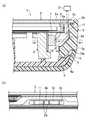
上記発光素子8からの照射光及び反射光を誘導する導光部材10は、正面側キャビネット3に嵌め込まれている。導光部材10は、図5に示すように、例えば透明なアクリル樹脂の一体成形品よりなり、発光素子8からの照射光を誘導する発光部11と、反射光を誘導する反射部12と、これら発光部11及び反射部12を連結する連結部13とを有する。この連結部13の下面には、指でつまむための取付用突起14が一体に成形されている。このため小さな導光部材10であっても、この取付用突起14をつまんで正面側キャビネット3に導光部材10を簡単に嵌め込むことができるようになっている。図1に示すように、導光部材10は、例えば両面テープ15により、正面側キャビネット3に貼り付けられている。なお、導光部材10の正面及び下面を除く外周は、メッキ、蒸着、塗装等を施して反射率を上げるようにしてもよい。これにより、光の漏れや減衰を防ぎ、被検出物Dを検出する感度を上げることができる。 The
図1(b)及び図6に示すように、導光部材10の一部は、液晶表示部2のガラスカバー2aを外したときに、正面側キャビネット3の上側周縁に形成したセンサ用開口3cから覗くことができる。なお、ガラスカバー2aの周縁には、黒色印刷が施されているが、概ねセンサ用開口3cに相当する範囲には、別工程によりIRインクにて印刷が行われており、ガラスカバー2aで正面側キャビネット3を覆ったときには、このセンサ用開口3cを肉眼で確認しにくくして見映えをよくしている。 As shown in FIGS. 1B and 6, a part of the
このセンサ用開口3cの奥側に発光部11と反射部12との間に挿入される遮光リブ3bが一体成形されている。この遮光リブ3bによって正面側キャビネット3の内部に一部が2つに枝分かれした導光用通路3dが形成されている。図1(a)に示すように、センサ用開口3cが正面側に形成され、近接センサ7が、このセンサ用開口3cよりも下側の位置に上方に向いて配置されていることから、導光用通路3dは、側面視L字状に折れ曲がっている。そして、導光部材10は、この導光用通路3dに嵌め込まれ、発光部11及び反射部12が遮光リブ3bを含む導光用通路3dで覆われている。これにより、遮光リブ3bが発光部11と反射部12との間での光の通過を確実に防止するので、検出精度が向上している。 A
導光用通路3dのセンサ用開口3cに近い部分は、金属製フレーム3aのプレス成形されて正面側に折り曲げられた縦壁部分で構成されている。このように、金属製フレーム3aであれば、剛性が高い上に光を通さないので、薄い壁面によって導光用通路3dを形成できる。 The portion of the
また、導光用通路3dにおける発光部11及び反射部12内で光を反射させる反射面のうち、特に背面に向かって下方へ折れ曲がっている反射面10aでは、照射光及び反射光をそれぞれ反射する役割を果たしている。このため、その裏側に対応する正面側キャビネット3の当接面3eは、黒色着色、シボ等による凹凸などにより、正面側キャビネット3の他の領域よりも反射率が低減されている。これにより、光の漏れや減衰を防ぎ、被検出物Dを検出する感度を上げることができるようになっている。 Of the reflecting surfaces that reflect light in the
このように、本実施形態では、導光部材10を設けることで光路変更の自由度が高まるので、被検出物Dの真正面に発光素子8及び受光素子9を配置する必要がなくなり、配置スペースを小さくすることができる。また、導光部材10の発光部11と反射部12とを分割することで、照射光と反射光とが別々の光路を通るので、検出精度を上げることができると共に、連結部13で連結されているので、取付が容易である。 Thus, in this embodiment, since the light path changing degree of freedom increases by providing the
したがって、本実施形態に係る携帯電話機1によると、発光素子8からの照射光を誘導する発光部11と、反射光を受光素子9に誘導する反射部12と、これらを連結する連結部13とを有する導光部材10を正面側キャビネット3に嵌め込むようにしたことにより、携帯電話機1のサイズを大きくすることなく、近接センサ7の検出精度を高めることができる。 Therefore, according to the
−変形例1−
図7は本発明の実施形態の変形例1を示し、導光部材10’の形状が異なる点で上記実施形態と異なる。なお、以下の各変形例では、図1〜図6と同じ部分については同じ符号を付してその詳細な説明は省略する。-Modification 1-
FIG. 7 shows a first modification of the embodiment of the present invention, which differs from the above embodiment in that the shape of the
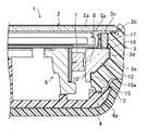
すなわち、本変形例の導光部材10’は、センサ用開口3cの周縁近傍まで直線状に伸びる延長部16を有する。この延長部16は、発光部11及び反射部12のそれぞれの先端から伸びている。延長部16を設けることで、被検出物Dと延長部16先端とが近付き、被検出物Dを検出する際の指向性がさらに向上している。 That is, the
−変形例2−
図8は本発明の実施形態の変形例2を示し、導光部材10”の形状が異なる点で上記実施形態と異なる。-Modification 2-
FIG. 8 shows a second modification of the embodiment of the present invention, which differs from the above embodiment in that the shape of the
すなわち、本変形例の導光部材10”は、センサ用開口3cの周縁近傍に嵌め込まれる第2導光部材17を有する。この第2導光部材17は、遮光リブ3bによって分離されている領域を含め、正面側から嵌め込まれる。図9に示すように、第2導光部材17は、正面側が左右に広がっており、広範囲の反射光を受光できるようになっている。第2導光部材17と導光部材10”とは、OCA両面テープ18で貼り付けられている。これにより、第2導光部材17の固定が行えると共に、感度の低下を防止できる。OCA両面テープ18の代わりに導光ゲルを用いれば、取り扱いが楽である。遮光リブ3bによって第2導光部材17の位置決めを行うことができると共に、照射光及び反射光を分割できるので、感度がよい。 That is, the
(その他の実施形態)
本発明は、実施形態について、以下のような構成としてもよい。(Other embodiments)
The present invention may have the following configurations for the embodiments.
すなわち、実施形態では、近接センサ7及び導光部材10を携帯電話機1の上側に配置し、正面に向かって照射光を放つようにしたが、近接センサ7及び導光部材10を別の位置に設けてもよく、照射光の方向も特に限定されない。 That is, in the embodiment, the
実施形態では、電子機器は、携帯電話機1としたが、PHS(Personal Handy-phone System)、PDA(Personal Digital Assistant)、スマートフォン、パソコン、モバイルツール、電子辞書、電卓、ゲーム機等であってもよく、液晶ディスプレイ、液晶テレビ、ブルーレイ(DVD)レコーダ等であってもよい。 In the embodiment, the electronic device is the
なお、以上の実施形態は、本質的に好ましい例示であって、本発明、その適用物や用途の範囲を制限することを意図するものではない。また、各実施形態に記載された技術的特徴は、互いに組合せ可能であり、組み合わせることにより、新しい技術的特徴を形成することができる。 In addition, the above embodiment is an essentially preferable illustration, Comprising: It does not intend restrict | limiting the range of this invention, its application thing, or a use. The technical features described in each embodiment can be combined with each other, and a new technical feature can be formed by combining them.
1 携帯電話機(電子機器)
2 液晶表示部
2a ガラスカバー
3 正面側キャビネット
3a 金属製フレーム
3b 遮光リブ
3c センサ用開口
3d 導光用通路
3e 当接面
4 背面側キャビネット
5 リアカバー
6 回路基板
7 近接センサ
8 発光素子
9 受光素子
10,10’,10” 導光部材
10a 反射面
11 発光部
12 反射部
13 連結部
14 取付用突起
15 両面テープ
16 延長部
17 第2導光部材
18 OCA両面テープ1 Mobile phone (electronic equipment)
2 Liquid crystal display
2a Glass cover
3 Front side cabinet
3a metal frame
3b Shading rib
3c Sensor opening
3d light guide passage
3e Contact surface
4 Rear cabinet
5 Rear cover
6 Circuit board
7 Proximity sensor
8 Light emitting elements
9 Light receiving element
10, 10 ', 10 "light guide member
10a Reflective surface
11 Light emitting part
12 Reflector
13 Connecting part
14 Mounting projection
15 Double-sided tape
16 Extension
17 Second light guide member
18 OCA double-sided tape
Claims (6)
Translated fromJapanese筐体に嵌め込まれ、上記発光素子からの照射光及び上記反射光を誘導する導光部材を有し、
上記導光部材は、上記照射光を誘導する発光部と、上記反射光を誘導する反射部と、該発光部及び反射部を連結する連結部とを有し、
上記筐体は、上記導光部材よりも透過率が低く、上記発光部と上記反射部との間に挿入されて該発光部と該反射部との間の光の通過を防止する遮光リブが一体成形されている
ことを特徴とする電子機器。In an electronic apparatus including a light emitting element and a proximity sensor having a light receiving element that receives reflected light of light emitted from the light emitting element and detects an object to be detected.
A light guide member that is fitted into a housing and guides the light emitted from the light emitting element and the reflected light;
The light guide member maypossess a light emitting unit to induce the irradiation light, a reflecting unit for inducing the reflected light, and a connecting portion for connecting the light emitting portion and the reflectiveportion,
The housing has a light transmittance rib lower than that of the light guide member, and a light-shielding rib that is inserted between the light emitting unit and the reflecting unit to prevent light from passing between the light emitting unit and the reflecting unit. An electronic device characterizedby being integrally molded .
上記発光部及び上記反射部は、上記筐体に成形した導光用通路で覆われており、
上記導光用通路は、上記遮光リブによって枝分かれしている
ことを特徴とする電子機器。The electronic device according to claim1 ,
The light emitting part and the reflecting part are covered with a light guide passage formed in the casing,
The electronic apparatus, wherein the light guide passage is branched by the light shielding rib .
筐体に嵌め込まれ、上記発光素子からの照射光及び上記反射光を誘導する導光部材を有し、
上記導光部材は、上記照射光を誘導する発光部と、上記反射光を誘導する反射部と、該発光部及び反射部を連結する連結部とを有し、
上記発光部及び上記反射部は、上記筐体に成形した導光用通路で覆われ、
上記導光用通路における、上記発光部及び上記反射部内で光を反射させる反射面の裏側は、上記筐体の他の領域よりも反射率が低減されている
ことを特徴とする電子機器。In an electronic apparatus including a light emitting element and a proximity sensor having a light receiving element that receives reflected light of light emitted from the light emitting element and detects an object to be detected.
A light guide member that is fitted into a housing and guides the light emitted from the light emitting element and the reflected light;
The light guide member includes a light emitting part that guides the irradiation light, a reflective part that guides the reflected light, and a connecting part that connects the light emitting part and the reflective part,
The light emitting part and the reflecting part are covered with a light guide passage formed in the casing,
The electronic device according to claim 1, wherein a reflectance of a back side of a reflection surface that reflects light in the light emitting portion and the reflection portion in the light guide passage is reduced as compared with other regions of the casing.
上記筐体は、光を通さない金属製フレームがインサート成形されており、
上記導光用通路の少なくとも一部が上記金属製フレームで構成されている
ことを特徴とする電子機器。The electronic device according to claim2 or3 ,
The casing is insert-molded with a metal framethat does not transmitlight ,
An electronic apparatus, wherein at least a part of the light guide passage is constituted by the metal frame.
上記連結部における上記発光部及び反射部の反対側には、指でつまむための取付用突起が一体に成形されている
ことを特徴とする電子機器。In the electronic device according to any one of claims 1 to4 ,
On the opposite side of the light emitting portion and a reflective portion which definitive in the connecting portion, an electronic apparatus for mounting for pinch a finger projection is characterized in that it is integrally formed.
上記発光部及び反射部の先端部には、上記筐体に設けたセンサ用開口の周縁まで伸びる延長部が設けられている
ことを特徴とする電子機器。The electronic device according to any one of請Motomeko 1 to 5,
At the tip of the light emitting part and the reflecting part, an extension part extending to the periphery of the sensor opening provided in the housing is provided.
An electronic device characterized by that.
Priority Applications (1)
| Application Number | Priority Date | Filing Date | Title |
|---|---|---|---|
| JP2013195855AJP6170392B2 (en) | 2013-09-20 | 2013-09-20 | Electronics |
Applications Claiming Priority (1)
| Application Number | Priority Date | Filing Date | Title |
|---|---|---|---|
| JP2013195855AJP6170392B2 (en) | 2013-09-20 | 2013-09-20 | Electronics |
Publications (2)
| Publication Number | Publication Date |
|---|---|
| JP2015061291A JP2015061291A (en) | 2015-03-30 |
| JP6170392B2true JP6170392B2 (en) | 2017-07-26 |
Family
ID=52818468
Family Applications (1)
| Application Number | Title | Priority Date | Filing Date |
|---|---|---|---|
| JP2013195855AExpired - Fee RelatedJP6170392B2 (en) | 2013-09-20 | 2013-09-20 | Electronics |
Country Status (1)
| Country | Link |
|---|---|
| JP (1) | JP6170392B2 (en) |
Families Citing this family (4)
| Publication number | Priority date | Publication date | Assignee | Title |
|---|---|---|---|---|
| JP2015079095A (en)* | 2013-10-16 | 2015-04-23 | 三菱電機株式会社 | Electrical apparatus |
| JP6491028B2 (en)* | 2015-04-23 | 2019-03-27 | シャープ株式会社 | Electronics |
| JP2018180850A (en)* | 2017-04-11 | 2018-11-15 | アルパイン株式会社 | Display device |
| WO2020179784A1 (en)* | 2019-03-04 | 2020-09-10 | 日本精機株式会社 | Display device |
Family Cites Families (5)
| Publication number | Priority date | Publication date | Assignee | Title |
|---|---|---|---|---|
| JP4746168B2 (en)* | 2000-04-25 | 2011-08-10 | 京セラ株式会社 | Mobile device |
| KR20100081052A (en)* | 2009-01-05 | 2010-07-14 | 삼성전자주식회사 | Detecting apparatus using a proximity sensor and mobile device having the same |
| JP5261320B2 (en)* | 2009-08-21 | 2013-08-14 | シャープ株式会社 | Optical distance measuring sensor and electronic device equipped with the same |
| US8761830B2 (en)* | 2011-03-15 | 2014-06-24 | Sony Corporation | Proximity sensor and portable terminal |
| JP2013187152A (en)* | 2012-03-09 | 2013-09-19 | Sharp Corp | Push button switch structure and electronic apparatus including the same |
- 2013
- 2013-09-20JPJP2013195855Apatent/JP6170392B2/ennot_activeExpired - Fee Related
Also Published As
| Publication number | Publication date |
|---|---|
| JP2015061291A (en) | 2015-03-30 |
Similar Documents
| Publication | Publication Date | Title |
|---|---|---|
| US11455018B2 (en) | Optical proximity sensor component comprising light guide | |
| KR20240042387A (en) | Electronic device including acoustic module | |
| CN107886927B (en) | electronic device | |
| JP5792348B1 (en) | Position input device and touch panel | |
| KR102763576B1 (en) | Electronic device incluidng optical sensor module | |
| TWI570400B (en) | Optical detecting device capable of preventing light leakage | |
| TWI526898B (en) | Optical touch panel and light guide module thereof | |
| JP2009176271A (en) | Optical joy stick and portable electronic equipment which includes it | |
| CN107978261B (en) | Electronic device | |
| JP6170392B2 (en) | Electronics | |
| US20110267314A1 (en) | Optical touch-sensing display module | |
| US8692146B2 (en) | Touchpad of an electronic apparatus and method for manufacturing the same | |
| JP2014029372A (en) | Electronic device | |
| CN109040362B (en) | Electronic device and method for assembling electronic device | |
| US20120262422A1 (en) | Optical touch module and method thereof | |
| CN210123563U (en) | Display screen assembly and electronic equipment | |
| TW201409124A (en) | Integrated backlight module and display device using the same | |
| US20150002473A1 (en) | Optical Touch Panel Device and Optical Touch Panel System Incorporating the Same | |
| CN111294435B (en) | mobile terminal | |
| CN107077620A (en) | Optical fingerprint imaging system and optical components | |
| TWI589906B (en) | Portable electronic device and proximity optical sensor module thereof | |
| CN107945662B (en) | Displays, Display Components and Electronic Equipment | |
| JP2013218677A (en) | Touch device and touch projection system | |
| KR101021072B1 (en) | Optical joysticks and portable electronic devices having the same | |
| CN210864742U (en) | Biometric detection system and electronic equipment |
Legal Events
| Date | Code | Title | Description |
|---|---|---|---|
| A621 | Written request for application examination | Free format text:JAPANESE INTERMEDIATE CODE: A621 Effective date:20160331 | |
| A977 | Report on retrieval | Free format text:JAPANESE INTERMEDIATE CODE: A971007 Effective date:20170113 | |
| A131 | Notification of reasons for refusal | Free format text:JAPANESE INTERMEDIATE CODE: A131 Effective date:20170214 | |
| A521 | Request for written amendment filed | Free format text:JAPANESE INTERMEDIATE CODE: A523 Effective date:20170404 | |
| TRDD | Decision of grant or rejection written | ||
| A01 | Written decision to grant a patent or to grant a registration (utility model) | Free format text:JAPANESE INTERMEDIATE CODE: A01 Effective date:20170613 | |
| A61 | First payment of annual fees (during grant procedure) | Free format text:JAPANESE INTERMEDIATE CODE: A61 Effective date:20170630 | |
| R150 | Certificate of patent or registration of utility model | Ref document number:6170392 Country of ref document:JP Free format text:JAPANESE INTERMEDIATE CODE: R150 | |
| LAPS | Cancellation because of no payment of annual fees |