JP6167646B2 - Information processing apparatus, control circuit, control program, and control method - Google Patents
Information processing apparatus, control circuit, control program, and control methodDownload PDFInfo
- Publication number
- JP6167646B2 JP6167646B2JP2013096046AJP2013096046AJP6167646B2JP 6167646 B2JP6167646 B2JP 6167646B2JP 2013096046 AJP2013096046 AJP 2013096046AJP 2013096046 AJP2013096046 AJP 2013096046AJP 6167646 B2JP6167646 B2JP 6167646B2
- Authority
- JP
- Japan
- Prior art keywords
- data
- value
- unit
- stored
- count value
- Prior art date
- Legal status (The legal status is an assumption and is not a legal conclusion. Google has not performed a legal analysis and makes no representation as to the accuracy of the status listed.)
- Expired - Fee Related
Links
Images


Classifications
- G—PHYSICS
- G06—COMPUTING OR CALCULATING; COUNTING
- G06F—ELECTRIC DIGITAL DATA PROCESSING
- G06F12/00—Accessing, addressing or allocating within memory systems or architectures
- G06F12/02—Addressing or allocation; Relocation
- G06F12/0223—User address space allocation, e.g. contiguous or non contiguous base addressing
- G06F12/023—Free address space management
- G06F12/0238—Memory management in non-volatile memory, e.g. resistive RAM or ferroelectric memory
- G06F12/0246—Memory management in non-volatile memory, e.g. resistive RAM or ferroelectric memory in block erasable memory, e.g. flash memory
- G—PHYSICS
- G11—INFORMATION STORAGE
- G11C—STATIC STORES
- G11C16/00—Erasable programmable read-only memories
- G11C16/02—Erasable programmable read-only memories electrically programmable
- G11C16/06—Auxiliary circuits, e.g. for writing into memory
- G11C16/34—Determination of programming status, e.g. threshold voltage, overprogramming or underprogramming, retention
- G11C16/349—Arrangements for evaluating degradation, retention or wearout, e.g. by counting erase cycles
- G11C16/3495—Circuits or methods to detect or delay wearout of nonvolatile EPROM or EEPROM memory devices, e.g. by counting numbers of erase or reprogram cycles, by using multiple memory areas serially or cyclically
- G—PHYSICS
- G06—COMPUTING OR CALCULATING; COUNTING
- G06F—ELECTRIC DIGITAL DATA PROCESSING
- G06F2212/00—Indexing scheme relating to accessing, addressing or allocation within memory systems or architectures
- G06F2212/72—Details relating to flash memory management
- G06F2212/7204—Capacity control, e.g. partitioning, end-of-life degradation
- G—PHYSICS
- G06—COMPUTING OR CALCULATING; COUNTING
- G06F—ELECTRIC DIGITAL DATA PROCESSING
- G06F2212/00—Indexing scheme relating to accessing, addressing or allocation within memory systems or architectures
- G06F2212/72—Details relating to flash memory management
- G06F2212/7207—Details relating to flash memory management management of metadata or control data
Landscapes
- Engineering & Computer Science (AREA)
- Theoretical Computer Science (AREA)
- Physics & Mathematics (AREA)
- General Engineering & Computer Science (AREA)
- General Physics & Mathematics (AREA)
- Memory System (AREA)
- Techniques For Improving Reliability Of Storages (AREA)
- Read Only Memory (AREA)
Description
Translated fromJapanese本発明は、情報処理装置、制御回路、制御プログラム、および制御方法に関する。 The present invention relates to an information processing device, a control circuit, a control program, and a control method.
従来、磁気ディスクよりも高速に動作する不揮発性メモリを用いた情報処理装置が知られている。このような情報処理システムの一例として、NANDフラッシュメモリデバイスをストレージ等の記憶装置として使用する情報処理装置が知られている。なお、以下の説明では、NANDフラッシュメモリデバイスをNANDデバイスと記載する。 Conventionally, an information processing apparatus using a nonvolatile memory that operates at a higher speed than a magnetic disk is known. As an example of such an information processing system, an information processing apparatus using a NAND flash memory device as a storage device such as a storage is known. In the following description, the NAND flash memory device is described as a NAND device.
ここで、NANDデバイスの各記憶領域は、情報を消去する際に劣化する。このため、頻繁に更新される情報が書込まれた記憶領域と、あまり更新されない情報が書込まれた記憶領域とでは、劣化する速度にばらつきが存在する。また、NANDデバイスは、情報を書込んだままにしておくと、データを書込んだ記憶領域の素子から電荷が抜け、ビット化けを発生させる場合がある。 Here, each storage area of the NAND device deteriorates when information is erased. For this reason, there is a variation in the deterioration speed between the storage area in which frequently updated information is written and the storage area in which information that is not updated much is written. In addition, if the NAND device is left written with information, the charge may be lost from the element in the storage area where the data is written, which may cause bit corruption.
かかる記憶領域の劣化を平準化したり、各記憶領域の素子から電荷が抜けることによるビット化けを防ぐため、情報を書込んだ際の時刻を記憶し、記憶した時刻と現在の時刻との比較結果に応じて情報の再書込みを行う技術が知られている。例えば、情報処理装置は、記憶領域ごとに、情報を書込んだ際の時刻を記憶する。そして、情報処理装置は、記憶した時刻と現在の時刻とを比較し、情報を書込んでから経過した経過時間を演算する。その後、情報処理装置は、経過時間と所定の閾値との比較結果に応じて、情報の再書込みを実行するか否か判定する。 Stores the time when the information was written in order to level the deterioration of the storage area and prevent bit corruption due to the loss of charge from the elements in each storage area, and the comparison result between the stored time and the current time A technique for rewriting information in response to the above is known. For example, the information processing apparatus stores the time when information is written for each storage area. Then, the information processing apparatus compares the stored time with the current time, and calculates the elapsed time that has elapsed since the information was written. Thereafter, the information processing apparatus determines whether to rewrite information according to a comparison result between the elapsed time and a predetermined threshold.
しかしながら、上述した情報の再書込みを実行する技術では、記憶領域ごとに、情報を書込んだ時刻をそのまま記憶するので、経過時間を演算するために記憶する時刻の総情報量が増大するという問題がある。 However, in the above-described technology for rewriting information, the time when information is written is stored as it is for each storage area, so that the total amount of information stored for calculating elapsed time increases. There is.
例えば、時刻の総情報量が増大した場合は、時刻を記憶する記憶装置の規模が増大するので、情報処理装置の回路規模が増大する。また、時刻の総情報量が増大すると、判定対象となる記憶領域にデータを書込んだ際の時刻を検索する時間が増大するので、NANDデバイスに対するアクセス性能が低下する。 For example, when the total amount of information at the time increases, the scale of the storage device that stores the time increases, so the circuit scale of the information processing apparatus increases. Further, when the total amount of information increases, the time for searching for the time when data is written to the storage area to be determined increases, and the access performance to the NAND device decreases.
1つの側面では、データを書込んだ時刻を示す情報の情報量を削減する情報処理装置、制御回路、制御プログラム、および制御方法を提供することを目的とする。 In one aspect, an object is to provide an information processing apparatus, a control circuit, a control program, and a control method that reduce the amount of information indicating the time at which data is written.
一態様の情報処理装置は、記憶装置を有する。また、情報処理装置は、記憶装置が有する複数の記憶領域の各々に記憶されたデータが移動の対象であるか判定する処理が、記憶装置が記憶する全てのデータに対して実行されるとカウント値を更新する計数部を有する。また、情報処理装置は、記憶装置にデータが書込まれる際に、計数部のカウント値をデータと対応付けて記憶する計数値記憶部を有する。また、情報処理装置は、記憶装置が記憶するデータごとに、計数値記憶部が記憶する値と計数部のカウント値とを比較して、各データが移動の対象であるか判定する判定部を有する。また、情報処理装置は、記憶装置に対して発行されたデータの読出し要求、または、記憶装置に対して発行されたデータの書込み要求の数を計数する要求計数部を有する。また、情報処理装置は、要求計数部が計数した読出し要求の数、または、書込み要求の数に応じて、データが移動の対象であるか判定するための閾値を設定する設定部を有する。また、判定部は、計数部のカウント値に設定部が設定した閾値を加算した値が、計数値記憶部が記憶する値以上となる場合は、当該値と対応付けて計数値記憶部が記憶するデータが移動の対象であると判定する。An information processing apparatus according to one embodiment includes a storage device. In addition, the information processing apparatus counts when the process of determining whether the data stored in each of the plurality of storage areas of the storage device is the object of movement is executed for all the data stored in the storage device. A counting unit for updating the value is included. In addition, the information processing apparatus includes a count value storage unit that stores the count value of the count unit in association with the data when data is written to the storage device. Further, the information processing device compares a value stored in the count value storage unit with a count value of the count unit for each data stored in the storage device, and determines a determination unit that determines whether each data is a target of movement. Have.The information processing apparatus also includes a request counting unit that counts the number of data read requests issued to the storage device or data write requests issued to the storage device. In addition, the information processing apparatus includes a setting unit that sets a threshold value for determining whether data is a target of movement according to the number of read requests or the number of write requests counted by the request counting unit. In addition, when the value obtained by adding the threshold set by the setting unit to the count value of the counting unit is equal to or greater than the value stored in the count value storage unit, the determination unit stores the count value storage unit in association with the value. It is determined that the data to be moved is the object of movement.
一実施形態によれば、データを書込んだ時刻を示す情報の情報量を削減できる。 According to one embodiment, it is possible to reduce the amount of information indicating the time when data is written.
以下に添付図面を参照して本願に係る情報処理装置、制御回路、制御プログラム、および制御方法の実施例を図面に基づいて詳細に説明する。なお、以下の実施例により開示技術が限定されるものではない。また、各実施例は、矛盾しない範囲で適宜組みあわせてもよい。 Hereinafter, embodiments of an information processing apparatus, a control circuit, a control program, and a control method according to the present application will be described in detail with reference to the accompanying drawings. The disclosed technology is not limited by the following embodiments. In addition, the embodiments may be combined as appropriate within a consistent range.
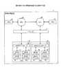
以下の実施例1では、図1を用いて、本願に係る情報処理装置の一例を説明する。図1は、実施例1に係る情報処理装置を説明する図である。図1に示す例では、情報処理装置1は、複数のメモリ2a、2b、複数のCPU(Central Processing Unit)3a、3b、I/O(Input Output)ハブ4、複数のSSD(Solid State Drive)5a、5bを有する。また、SSD5aは、NANDコントローラ6a、および複数のNANDデバイス7a〜10aを有する。 In Example 1 below, an example of an information processing apparatus according to the present application will be described with reference to FIG. FIG. 1 is a diagram illustrating the information processing apparatus according to the first embodiment. In the example shown in FIG. 1, the
また、SSD5bは、NANDコントローラ6b、および複数のNANDデバイス7b〜10bを有する。なお、以下の説明では、NANDコントローラ6b、および複数のNANDデバイス7b〜10bは、NANDコントローラ6a、および複数のNANDデバイス7a〜10aと同様の機能を発揮するものとして、説明を省略する。 The
各メモリ2a、2bは、各CPU3a、3bが演算処理に用いるデータを記憶する記憶装置である。また、各CPU3a、3bは、メモリ2a、2bが記憶するデータを用いて、各種演算処理を行う演算処理装置である。例えば、CPU3a、3bは、NUMA(Non-Uniform Memory Access)の技術を用いて、メモリ2a、2bが記憶するデータを取得し、取得したデータを用いて演算処理を実行する。 The
また、CPU3a、3bは、I/Oハブ4を介して、各SSD5a、5bが記憶するデータを取得し、取得したデータを用いて演算処理を実行する。詳細には、CPU3aは、SSD5aに対し、データの読出し要求や書込み要求を発行し、各NANDデバイス7a〜10aからデータの読出しや書込みを行う。例えば、CPU3aは、SSD5aに対し、読出し対象となるデータを指定する論理アドレスが格納された読出し要求を発行する。また、CPU3aは、データの書込み先を指定する論理アドレスと、書込み対象となるデータとが格納された書込み要求を発行する。 Further, the CPUs 3a and 3b acquire data stored in the
NANDデバイス7aは、各種データを記憶する不揮発性メモリである。詳細には、NANDデバイス7aは、データの記憶領域であるページを複数有し、ページ単位でデータの書込みを行う。また、NANDデバイス7aは、複数のページを有するブロックを複数有し、ブロック単位でデータの消去を行う。 The
NANDコントローラ6aは、各NANDデバイス7a〜10aに対してアクセスし、データの読出しや書込みを行う。例えば、NANDコントローラ6aは、各CPU3a、3bがデータが記憶された記憶領域を指定する際に用いる論理アドレスと、データが格納されたNANDデバイス7a〜10aの記憶領域を示す物理アドレスとを対応付けたアドレス変換テーブルを有する。 The
そして、NANDコントローラ6aは、読出し要求とともに論理アドレスを受信すると、アドレス変換テーブルを用いて、論理アドレスと対応付けられた物理アドレスを識別し、識別した物理アドレスが示す記憶領域からデータの読出しを行う。その後、NANDコントローラ6aは、I/Oハブ4を介して、読出したデータをCPU3aに送信する。 When the
なお、以下の説明では、理解を容易にするため、各ページの先頭アドレスとなる論理アドレスを単に論理アドレスと記載し、各ページの先頭アドレスとなる物理アドレスを単に物理アドレスと記載する。また、情報処理装置1が実行するシステムは、各ページの先頭アドレスとなる論理アドレスに対する読出し要求や書込み要求を発行するものとする。 In the following description, in order to facilitate understanding, a logical address that is the top address of each page is simply described as a logical address, and a physical address that is the top address of each page is simply described as a physical address. In addition, the system executed by the
例えば、NANDコントローラ6aは、NANDデバイス7a〜10aが、複数のブロックを有し、各ブロックに2q個のページが含まれている場合は、以下の処理を行う。まず、NANDコントローラ6aは、論理アドレスの下位qビットを論理的な1つのブロック内において、ページを識別するための論理ページ番号とし、残りの論理アドレスの上位pビットを論理的な1つのブロックを示す論理ブロックアドレスとする。For example,
また、NANDコントローラ6aは、物理アドレスの上位pビットを物理的な1つのブロックを示す物理ブロックアドレスとし、物理アドレスの下位qビットを物理的な1つのブロック内において、各ページを識別するための物理ページ番号とする。つまり、NANDコントローラ6aは、論理アドレスを、論理ブロックを示す論理ブロックアドレスと、論理ページを論理ブロックごとに示す論理ページ番号とに分割する。また、NANDコントローラ6aは、物理アドレスを、物理ブロックを示す物理ブロックアドレスと、物理ページを物理ブロックごとに示す物理ページ番号とに分割する。 Further, the
例えば、図2は、メモリアクセスの一例を説明する図である。なお、図2に示す例では、理解を容易にするため、ブロック数を「8」とし、各ブロック内のページ数が「4」のNANDデバイス7aについて記載した。また、図2に示す例では、論理ブロックアドレスと物理ブロックアドレスとを対応付けたアドレス変換テーブルを有するNANDコントローラ6aが実行する処理について記載した。 For example, FIG. 2 is a diagram illustrating an example of memory access. In the example illustrated in FIG. 2, the
例えば、CPU3aが実行するファイルシステムは、図2中(a)に示すように、論理ブロックアドレス「L4」に含まれる論理ページのうち、論理ページ番号「1」が示す論理ページに対する書込み要求を発行する。すなわち、ファイルシステムは、論理アドレス「L4−1」に対する書込み要求を発行する。すると、NANDコントローラ6aは、図2中(b)に示すように、論理ブロックアドレス「L4」に対応付けられた物理ブロックアドレス「P7」を取得し、図2中(c)に示すように、書込み対象となるページを含むブロックを識別する。 For example, the file system executed by the CPU 3a issues a write request for the logical page indicated by the logical page number “1” among the logical pages included in the logical block address “L4”, as shown in FIG. To do. That is, the file system issues a write request for the logical address “L4-1”. Then, the
続いて、NANDコントローラ6aは、図2中(d)に示すように、物理ブロックアドレス「P7」が示す物理ブロックの全データを予備ブロックにコピーする。この際、NANDコントローラ6aは、書込み要求の対象となる論理ページ番号「1」と同じ物理ページ番号「1」のデータを書込み対象となるデータで更新する。その後、NANDコントローラ6aは、図2中(e)に示すように、論理ブロックアドレス「L4」と対応付けられていた物理ブロックアドレス「P7」を予備ブロックの物理ブロックアドレス「P8」に更新する。そして、NANDコントローラ6aは、物理ブロックアドレス「P7」が示すブロックのデータを消去する。 Subsequently, as shown in FIG. 2D, the
ここで、従来のNANDコントローラは、劣化速度のばらつきを平準化したり、電荷が素子から抜けることで発生するビット化けを防ぐため、NANDデバイスの各ブロックにデータを書込んだ際の時刻をタイムスタンプとして記憶する。そして、従来のNANDコントローラは、各ブロックについて、記憶したタイムスタンプと現在の時刻との差が所定の閾値よりも大きい場合は、ブロックに格納されたデータを他のブロックに移動することで、データの再書込みを行う。 Here, the conventional NAND controller time-stamps the time when data was written to each block of the NAND device in order to level out the variation in the deterioration rate and prevent bit corruption that occurs when charges escape from the element. Remember as. When the difference between the stored time stamp and the current time is greater than a predetermined threshold for each block, the conventional NAND controller moves the data stored in the block to another block, thereby transferring the data Rewrite of.
以下、図3を用いて、従来のNANDコントローラが実行する処理の一例を説明する。図3は、従来のNANDコントローラが実行する処理の一例を説明する図である。例えば、NANDコントローラは、図3中(f)に示すように、I/Oハブから読出し又は書込み要求を受信する。すると、NANDコントローラは、読出し/書込み制御を実行する。例えば、NANDコントローラは、図3中(g)に示すように、アドレス変換テーブルを用いて論理アドレスを物理アドレスに変換する。そして、NANDコントローラは、図3中(h)に示すように、変換後の論理アドレスを用いて、NANDデバイスに対する読出しや書込み処理を実行する。 Hereinafter, an example of processing executed by a conventional NAND controller will be described with reference to FIG. FIG. 3 is a diagram for explaining an example of processing executed by a conventional NAND controller. For example, the NAND controller receives a read or write request from the I / O hub, as shown at (f) in FIG. Then, the NAND controller executes read / write control. For example, the NAND controller converts a logical address into a physical address using an address conversion table as shown in (g) of FIG. Then, as shown in (h) of FIG. 3, the NAND controller executes read and write processing for the NAND device using the converted logical address.
ここで、NANDコントローラは、NANDデバイスが有する各ブロックの物理アドレスと、データの書込みを行ったか否かを示すバリッドビットと、データの書込みを行った時刻を示すタイムスタンプとを対応付けた管理情報テーブルを有する。そして、NANDコントローラは、NANDデバイスに対する書込み処理を実行した場合は、図3中(i)に示すように、書込み処理を行った時刻と、データを書込んだブロックと、バリッドビットとを対応付けて管理情報テーブルに格納する。例えば、NANDコントローラは、図3中(j)に示すように、データの書込みを行った際に時刻カウンタがカウントしていた時刻と、データの書込みを行ったブロックの物理ブロックアドレスと、バリッドビット「1」とを対応付けて管理情報テーブルに格納する。 Here, the NAND controller associates the physical address of each block of the NAND device, the valid bit indicating whether or not data has been written, and the time stamp indicating the time when the data has been written. Has a table. When the NAND controller executes the write process to the NAND device, as shown in FIG. 3 (i), the NAND controller associates the write process time, the block in which the data is written, and the valid bit. Stored in the management information table. For example, the NAND controller, as shown in FIG. 3 (j), shows the time counted by the time counter when data was written, the physical block address of the block where data was written, and the valid bit. “1” is associated and stored in the management information table.
また、NANDコントローラは、データ移動制御を実行する。例えば、NANDコントローラは、図3中(k)に示すように、管理情報テーブルに格納された時刻と、時刻カウンタがカウントする現在の時刻とを比較し、書込まれてから所定の時間が経過したデータを識別する。そして、NANDコントローラは、図3中(l)に示すように、識別したデータを他のブロックに移動させる。その後、NANDコントローラは、図3中(m)に示すように、データの移動に応じて、アドレス変換テーブルを更新し、図3中(n)に示すように、管理情報テーブルを更新する。 Further, the NAND controller performs data movement control. For example, as shown in (k) in FIG. 3, the NAND controller compares the time stored in the management information table with the current time counted by the time counter, and a predetermined time has elapsed since the writing. Identified data. Then, the NAND controller moves the identified data to another block as indicated by (l) in FIG. Thereafter, the NAND controller updates the address conversion table in accordance with the movement of data as shown in (m) in FIG. 3, and updates the management information table as shown in (n) in FIG.
次に、図4を用いて、従来のNANDコントローラが、タイムスタンプを用いて移動するデータを識別する処理について説明する。図4は、従来のタイムスタンプを用いた処理を説明する図である。なお、図4には、従来のNANDコントローラが有する管理情報テーブルの内容と、時刻カウンタがカウントする値とを記載した。 Next, a process in which a conventional NAND controller identifies data to be moved using a time stamp will be described with reference to FIG. FIG. 4 is a diagram for explaining processing using a conventional time stamp. FIG. 4 shows the contents of the management information table of the conventional NAND controller and the values counted by the time counter.
例えば、NANDコントローラは、時刻カウント値が「12」の際に、物理ブロックアドレス「P1」が示すブロックにデータを書込んだ場合は、以下の処理を実行する。すなわち、NANDコントローラは、図4中(o)に示すように、物理ブロックアドレス「P1」とバリッドビット「1」とタイムスタンプ「12」を対応付けて格納する。 For example, when the time count value is “12”, the NAND controller executes the following processing when data is written in the block indicated by the physical block address “P1”. That is, the NAND controller stores the physical block address “P1”, the valid bit “1”, and the time stamp “12” in association with each other as shown in (o) of FIG.
また、NANDコントローラは、時刻カウント値が「810」の際に物理ブロックアドレス「P5」が示すブロックにデータを書込んだ場合は、以下の処理を実行する。すなわち、NANDコントローラは、図4中(p)に示すように、物理ブロックアドレス「P5」とバリッドビット「1」とタイムスタンプ「810」とを対応付けて管理情報テーブルに格納する。 In addition, when the time count value is “810”, the NAND controller executes the following processing when data is written in the block indicated by the physical block address “P5”. That is, the NAND controller stores the physical block address “P5”, the valid bit “1”, and the time stamp “810” in association with each other in the management information table, as shown in (p) of FIG.
また、NANDコントローラは、時刻カウント値が「5200」の際に物理ブロックアドレス「P6」が示すブロックにデータを書込んだ場合は、以下の処理を実行する。すなわち、NANDコントローラは、図4中(q)に示すように、物理ブロックアドレス「P6」とバリッドビット「1」とタイムスタンプ「5200」とを対応付けて管理情報テーブルに格納する。 In addition, when the time count value is “5200”, the NAND controller executes the following processing when data is written in the block indicated by the physical block address “P6”. That is, the NAND controller stores the physical block address “P6”, the valid bit “1”, and the time stamp “5200” in association with each other in the management information table, as indicated by (q) in FIG.
また、NANDコントローラは、所定の時間間隔で、管理情報テーブルに格納された各タイムスタンプの値を参照し、タイムスタンプの値と現在の時刻カウンタの値との差が所定の閾値よりも大きい物理ブロックを識別する。例えば、図4に示す例では、NANDコントローラは、現在の時刻カウンタの値「5510」との差分が大きいタイムスタンプ「12」が対応付けられた物理ブロックアドレス「P1」を識別する。そして、NANDコントローラは、物理ブロックアドレス「P1」が示すブロックのデータを、例えば、物理ブロックアドレス「P7」が示すブロックに移動させる。 In addition, the NAND controller refers to each time stamp value stored in the management information table at a predetermined time interval, and the difference between the time stamp value and the current time counter value is larger than a predetermined threshold value. Identify the block. For example, in the example illustrated in FIG. 4, the NAND controller identifies the physical block address “P1” associated with the time stamp “12” having a large difference from the current time counter value “5510”. Then, the NAND controller moves the data of the block indicated by the physical block address “P1” to, for example, the block indicated by the physical block address “P7”.
その後、NANDコントローラは、図4中(r)に示すように、物理ブロックアドレス「P7」と対応付けられたバリッドビットを「1」に更新し、タイムスタンプとして現在の時刻の値「5510」を対応付ける。また、NANDコントローラは、図4中(s)に示すように、物理ブロックアドレス「P1」と対応付けられたバリッドビットを「0」に更新し、タイムスタンプの値を削除する。 Thereafter, the NAND controller updates the valid bit associated with the physical block address “P7” to “1” as shown in (r) of FIG. 4, and sets the current time value “5510” as a time stamp. Associate. Further, as shown in (s) in FIG. 4, the NAND controller updates the valid bit associated with the physical block address “P1” to “0” and deletes the time stamp value.
しかしながら、従来のNANDコントローラは、各物理ブロックアドレスごとに、タイムスタンプを記憶するので、管理情報テーブルのデータサイズを増大させてしまう。例えば、NANDコントローラは、1ページの大きさが8キロバイトで、1つのブロックに128ページが含まれる場合は、1メガバイトごとに複数桁のタイムスタンプを管理情報テーブルに格納する。このため、NANDデバイス7a〜10aの容量が多くなるほど、管理情報テーブルのサイズが大きくなる。この結果、従来のNANDコントローラは、管理情報テーブルを記憶するために回路規模が増大したり、タイムスタンプを参照する際の時間が増大し、NANDデバイスに対するアクセス性能を低下させてしまう。 However, since the conventional NAND controller stores a time stamp for each physical block address, the data size of the management information table is increased. For example, when the size of one page is 8 kilobytes and 128 pages are included in one block, the NAND controller stores a multi-digit time stamp for each megabyte in the management information table. For this reason, the size of the management information table increases as the capacity of the
なお、管理情報テーブルのデータサイズを減少させるため、所定の桁数で時刻カウンタの値を初期値に戻す方法が考えられる。しかしながら、所定の桁数で時刻カウンタの値を初期値に戻した場合は、時刻カウンタの値が一巡した際に、誤動作が発生する場合がある。以下、図5を用いて、時刻カウンタの値が一巡した際に発生する誤動作の一例について説明する。 In order to reduce the data size of the management information table, a method of returning the value of the time counter to the initial value by a predetermined number of digits is conceivable. However, when the value of the time counter is returned to the initial value with a predetermined number of digits, a malfunction may occur when the value of the time counter makes a round. Hereinafter, an example of a malfunction that occurs when the value of the time counter makes a round will be described with reference to FIG.
図5は、従来のタイムスタンプを用いた処理の問題を説明する図である。なお、図5に示す例では、時刻カウンタの値が「9999」で桁あふれを起こし、初期値「0」に戻る例について説明する。例えば、NANDコントローラは、図5中(t)に示すように、時刻カウンタの値が「12」、「810」、「5200」の際に、物理ブロックアドレス「P1」、「P5」、「P6」が示すブロックにデータを書込んだ旨を管理情報テーブルに格納する。 FIG. 5 is a diagram for explaining a problem of processing using a conventional time stamp. In the example illustrated in FIG. 5, an example will be described in which the value of the time counter is “9999” and overflows and returns to the initial value “0”. For example, as shown in (t) of FIG. 5, the NAND controller has physical block addresses “P1”, “P5”, “P6” when the value of the time counter is “12”, “810”, “5200”. Is stored in the management information table.
続いて、NANDコントローラは、図5中(u)に示すように、時刻カウンタの値が「8100」の際に、物理ブロックアドレス「P2」が示すブロックにデータを書込んだ旨を管理情報テーブルに格納する。また、NANDコントローラは、時刻カウンタの値が一巡し、「35」となった際に、物理ブロックアドレス「P3」が示すブロックにデータを書込んだ旨を管理情報テーブルに格納する。 Subsequently, as illustrated in (u) of FIG. 5, the NAND controller indicates that the data is written in the block indicated by the physical block address “P2” when the value of the time counter is “8100”. To store. The NAND controller stores in the management information table that data has been written to the block indicated by the physical block address “P3” when the value of the time counter has reached “35”.
そして、NANDコントローラは、図5中(v)に示すように、時刻カウンタの値が「50」の際に、各タイムスタンプの値を参照し、時刻カウンタの値が一巡することを考慮して、時刻カウンタの値「50」と差分が大きいタイムスタンプを検索する。ここで、NANDデバイス7a〜10aが記憶するデータのうち、最も古いデータは、タイムスタンプ「12」と対応付けられた物理ブロックアドレス「P1」が示すブロックに格納されたデータである。 Then, as shown in FIG. 5 (v), the NAND controller refers to the value of each time stamp when the value of the time counter is “50”, and considers that the value of the time counter makes a round. A time stamp having a large difference from the time counter value “50” is searched. Here, among the data stored in the
しかしながら、NANDコントローラは、優先度が高い読出し要求や書込み要求が集中して発行された際に、データの移動処理が延期された場合や、移動処理の完了が遅れた場合等には、時刻カウンタの値がタイムスタンプの値を追い越す場合がある。かかる場合は、NANDコントローラは、タイムスタンプの値が、時刻カウンタの値が一巡する前の値であるか否かを判別できない。 However, the NAND controller does not provide a time counter when the data movement process is postponed or the completion of the movement process is delayed when read requests and write requests with high priority are issued in a concentrated manner. May overtake the timestamp value. In such a case, the NAND controller cannot determine whether or not the value of the time stamp is a value before the value of the time counter completes.
この結果、NANDコントローラは、図5中(w)に示すように、物理ブロックアドレス「P5」と対応付けられたタイムスタンプの値「810」が最も古いタイムスタンプの値であると判定する。そして、NANDコントローラは、物理ブロックアドレス「P5」と対応付けられたタイムスタンプの値「810」を削除する。また、NANDコントローラは、図5中(x)に示すように、物理ブロックアドレス「P5」が示すブロックに格納されていたデータを、物理ブロックアドレス「P7」が示すブロックに移動させる。 As a result, the NAND controller determines that the time stamp value “810” associated with the physical block address “P5” is the oldest time stamp value, as indicated by (w) in FIG. Then, the NAND controller deletes the time stamp value “810” associated with the physical block address “P5”. Further, as illustrated in (x) in FIG. 5, the NAND controller moves the data stored in the block indicated by the physical block address “P5” to the block indicated by the physical block address “P7”.
このように、従来のNANDコントローラは、図5中(y)に示すように、物理ブロックアドレス「P1」が示すブロックに格納されたデータが最も古いデータであるにもかかわらず、古いデータであると検出できない。そこで、実施例1に係るNANDコントローラ6aは、以下の処理を実行する。 Thus, as shown in FIG. 5 (y), the conventional NAND controller is old data even though the data stored in the block indicated by the physical block address “P1” is the oldest data. Cannot be detected. Therefore, the
まず、NANDコントローラ6aは、NANDデバイス7a〜10aが記憶するデータが移動の対象であるか判定する処理が、全てのデータに対して実行されると、カウント値を更新する巡回回数カウンタを有する。また、NANDコントローラ6aは、NANDデバイス7a〜10aにデータを書込む際に、巡回回数カウンタのカウント値を記憶する。詳細には、NANDコントローラ6aは、データの書込み先となるブロックの物理ブロックアドレスと巡回回数カウンタのカウント値とを対応付けて記憶する。 First, the
そして、NANDコントローラ6aは、データごとに、データが格納された物理ブロックアドレスと対応付けて記憶するカウント値と、巡回回数カウンタのカウント値とを比較して、各ブロックのデータが移動の対象であるか判定する。この結果、NANDコントローラ6aは、巡回回数カウンタが計数するカウント値の桁数を少なくしても、データ書込み時やデータ移動時に記憶したカウント値を追越す状態を防ぐことができる。 Then, for each data, the
次に、図6を用いて、NANDコントローラ6aが有する機能構成の一例について説明する。図6は、実施例1に係るNANDコントローラの機能構成を説明する図である。図6に示す例では、NANDコントローラ6aは、テーブル記憶部11、リクエスタインターフェース部12、リクエスト調停部13、テーブル制御部14、デバイスアクセス制御部15を有する。また、NANDコントローラ6aは、巡回回数カウンタ16、巡回参照制御部17、データ移動制御部18を有する。また、テーブル記憶部11は、アドレス変換テーブル19、管理情報テーブル20を記憶する。 Next, an example of a functional configuration of the
まず、図7、図8を用いて、テーブル記憶部11が記憶するアドレス変換テーブル19と、管理情報テーブル20に格納された情報について説明する。図7は、実施例1に係るアドレス変換テーブルに格納された情報の一例を説明する図である。図7に示すように、アドレス変換テーブル19には、論理ブロックアドレスと、物理ブロックアドレスとが対応付けて格納されている。 First, the information stored in the address conversion table 19 and the management information table 20 stored in the table storage unit 11 will be described with reference to FIGS. FIG. 7 is a schematic diagram illustrating an example of information stored in the address conversion table according to the first embodiment. As shown in FIG. 7, the address conversion table 19 stores a logical block address and a physical block address in association with each other.
例えば、図7に示す例では、アドレス変換テーブル19には、論理ブロックアドレス「L0」と物理ブロックアドレス「P4」とが対応付けて格納されている。すなわち、アドレス変換テーブル19は、物理ブロックアドレス「P4」が示すブロックに論理ブロックアドレス「L0」が指定するデータが格納されている旨を示す。 For example, in the example shown in FIG. 7, the address conversion table 19 stores the logical block address “L0” and the physical block address “P4” in association with each other. That is, the address conversion table 19 indicates that the data specified by the logical block address “L0” is stored in the block indicated by the physical block address “P4”.
同様に、図7に示す例では、アドレス変換テーブル19には、論理ブロックアドレス「L1」と物理ブロックアドレス「P2」とが対応付けて格納され、論理ブロックアドレス「L2」と物理ブロックアドレス「P3」とが対応付けて格納される。また、アドレス変換テーブル19には、論理ブロックアドレス「L3」と物理ブロックアドレス「P6」とが対応付けて格納され、論理ブロックアドレス「L4」と物理ブロックアドレス「P7」とが対応付けて格納される。 Similarly, in the example illustrated in FIG. 7, the address conversion table 19 stores the logical block address “L1” and the physical block address “P2” in association with each other, and the logical block address “L2” and the physical block address “P3”. Are stored in association with each other. The address conversion table 19 stores the logical block address “L3” and the physical block address “P6” in association with each other, and stores the logical block address “L4” and the physical block address “P7” in association with each other. The
また、アドレス変換テーブル19には、論理ブロックアドレス「L5」と物理ブロックアドレス「P1」とが対応付けて格納され、論理ブロックアドレス「L6」と物理ブロックアドレス「P0」とが対応付けて格納される。また、アドレス変換テーブル19には、論理ブロックアドレス「L7」と物理ブロックアドレス「P5」とが対応付けて格納される。 The address conversion table 19 stores the logical block address “L5” and the physical block address “P1” in association with each other, and stores the logical block address “L6” and the physical block address “P0” in association with each other. The The address conversion table 19 stores the logical block address “L7” and the physical block address “P5” in association with each other.
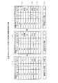
次に、図8を用いて、管理情報テーブル20に格納される情報について説明する。図8は、実施例1に係る管理情報テーブルに格納された情報の一例を説明する図である。図8に示すように、管理情報テーブル20には、物理ブロックアドレスと、バリッドビットと、タイムスタンプとが対応付けて格納される。ここで、バリッドビットとは、対応付けられた物理ブロックアドレスが示すブロックにデータが書込まれているか否かを示す情報である。また、タイムスタンプとは、対応付けられた物理ブロックアドレスが示すブロックにデータを書込んだ際に、巡回回数カウンタ16がカウントしていたカウント値である。すなわち、NANDコントローラ6aは、データを書込んだ際のカウント値を物理ブロックアドレスと対応付けて記憶する。 Next, information stored in the management information table 20 will be described with reference to FIG. FIG. 8 is a schematic diagram illustrating an example of information stored in the management information table according to the first embodiment. As shown in FIG. 8, the management information table 20 stores physical block addresses, valid bits, and time stamps in association with each other. Here, the valid bit is information indicating whether or not data is written in the block indicated by the associated physical block address. The time stamp is a count value counted by the
例えば、図8に示す例では、管理情報テーブル20には、物理ブロックアドレス「P0」と、バリッドビット「1」と、タイムスタンプ「2」とが対応付けて格納される。すなわち、管理情報テーブル20は、物理ブロックアドレス「P0」が示す記憶領域に対し、巡回回数カウンタ16のカウント値が「2」であったことを示す。 For example, in the example shown in FIG. 8, the management information table 20 stores the physical block address “P0”, the valid bit “1”, and the time stamp “2” in association with each other. That is, the management information table 20 indicates that the count value of the
同様に、図8に示す例では、管理情報テーブル20には、物理ブロックアドレス「P1」と、バリッドビット「1」と、タイムスタンプ「7」とが対応付けて格納される。また、管理情報テーブル20には、物理ブロックアドレス「P5」と、バリッドビット「1」と、タイムスタンプ「7」とが対応付けて格納される。このように、管理情報テーブル20には、データが書込まれた際の巡回回数カウンタ16の値が格納される。なお、管理情報テーブル20を記憶するテーブル記憶部11は、特許請求の範囲に記載の計数値記憶部の一例である。 Similarly, in the example shown in FIG. 8, the management information table 20 stores the physical block address “P1”, the valid bit “1”, and the time stamp “7” in association with each other. The management information table 20 stores the physical block address “P5”, the valid bit “1”, and the time stamp “7” in association with each other. As described above, the management information table 20 stores the value of the
図6に戻り、リクエスタインターフェース部12は、CPU3a、3bからNANDデバイス7a〜10aに対するリクエストのインターフェースである。例えば、リクエスタインターフェース部12は、CPU3a、3bからI/Oハブ4を介して、論理アドレスを含む読出し要求を受信する。かかる場合は、リクエスタインターフェース部12は、読出し要求をリクエスト調停部13に出力する。また、リクエスタインターフェース部12は、NANDデバイス7a〜10aから読出したデータをリクエスト調停部13から受信すると、読出し要求の発行元となるCPU3a、3bに対して、データを送信する。 Returning to FIG. 6, the
また、リクエスタインターフェース部12は、CPU3a、3bから、NANDデバイス7a〜10aに対して書込むデータと、書込み対象となるデータの論理アドレスとを含む書込み要求を受信する。かかる場合は、リクエスタインターフェース部12は、受信した書込み要求をリクエスト調停部13に出力する。また、リクエスタインターフェース部12は、リクエスト調停部13から、データ書込みが完了した旨の応答を受信すると、受信した応答を、書込み要求の発行元となるCPU3a、3bに対して、応答を送信する。 Further, the
リクエスト調停部13は、リクエスタインターフェース部12、データ移動制御部18、巡回参照制御部17が発行する各種リクエストの調停を行う。詳細には、リクエスト調停部13は、リクエスタインターフェース部12から受信する読出し要求、又は、書込み要求を受信する。また、リクエスト調停部13は、データ移動制御部18から、NANDデバイス7a〜10aが記憶するデータを、現在記憶するブロックから他のブロックに移動するよう要求する移動要求を受信する。また、リクエスト調停部13は、巡回参照制御部17から、管理情報テーブル20の参照を要求するテーブル参照要求を受信する。 The
そして、リクエスト調停部13は、リクエスタインターフェース部12、データ移動制御部18、巡回参照制御部17から受信する読出し要求、書込み要求、移動要求、テーブル参照要求の調停を行う。例えば、リクエスト調停部13は、CPU3a、3bからNANDデバイス7a〜10aに対するデータの読出しや書込みが阻害されないよう、リクエスタインターフェース部12が発行する読出し要求、および、書込み要求を最優先で実行する。また、例えば、リクエスト調停部13は、移動要求をテーブル参照要求よりも優先して実行する。なお、リクエスト調停部13が各要求を調停するルールについては、上述した処理に限定されるものではなく、任意のルールを適用してよい。 The
以下、リクエスト調停部13が読出し要求、書込み要求、移動要求、テーブル参照要求を受信した際に実行する処理の一例を説明する。例えば、リクエスト調停部13は、読出し要求を受信すると、読出し要求に含まれる論理アドレスをテーブル制御部14に出力する。そして、リクエスト調停部13は、テーブル制御部14から、読出し対象となる物理アドレスを受信すると、受信した物理アドレスを格納した読出し要求をデバイスアクセス制御部15に発行する。その後、リクエスト調停部13は、読出し対象となるデータをデバイスアクセス制御部15から受信すると、受信したデータをリクエスタインターフェース部12に出力する。 Hereinafter, an example of processing executed when the
また、リクエスト調停部13は、書込み要求を受信すると、書込み要求に含まれる論理アドレスをテーブル制御部14に出力する。この結果、リクエスト調停部13は、書込み対象のデータが新たなデータである場合は、データが格納されていない予備ブロックのうち、データの書込み先となるページの物理アドレスをテーブル制御部14から受信する。 Further, when receiving the write request, the
その後、リクエスト調停部13は、テーブル制御部14から受信した物理アドレスと、書込み対象のデータとを含む書込み要求をデバイスアクセス制御部15に発行する。また、リクエスト調停部13は、データの書込み先となるページの物理アドレスと、書込み要求に含まれる論理アドレスとを含むテーブル更新要求をテーブル制御部14に出力する。 Thereafter, the
また、リクエスト調停部13は、書込みがデータの更新を目的とする場合は、更新元のデータが格納されたページの物理アドレスを更新元物理アドレスとしてテーブル制御部14から受信する。また、リクエスト調停部13は、テーブル制御部14から、予備ブロックに含まれるページの物理アドレス、すなわちデータの書込み先となるページの物理アドレスを更新先物理アドレスとして受信する。 Further, when the write is intended to update the data, the
そして、リクエスト調停部13は、更新元物理アドレスと、更新先物理アドレスとをテーブル制御部14から受信した場合は、データの更新を要求する更新要求をデバイスアクセス制御部15に発行する。詳細には、リクエスト調停部13は、更新元物理アドレスと、更新先物理アドレスと、書込むデータとを含む更新要求をデバイスアクセス制御部15に発行する。 When the
また、リクエスト調停部13は、更新元物理アドレスと、更新先物理アドレスと、書込み要求に含まれる論理アドレスとを含むテーブル更新要求をテーブル制御部14に出力する。その後、リクエスト調停部13は、デバイスアクセス制御部15からデータの書込みが完了した旨の応答を受信すると、受信した応答をリクエスタインターフェース部12に出力する。 Further, the
また、リクエスト調停部13は、移動対象のデータが格納されたブロックの物理ブロックアドレスを含む移動要求を受信する。以下、移動対象のデータが格納されたブロックの物理ブロックアドレスを移動元物理ブロックアドレスと記載する。また、リクエスト調停部13は、テーブル制御部14に問い合わせる等して、予備ブロックの物理ブロックアドレス、すなわちデータの移動先となるブロックの物理ブロックアドレスを移動先物理ブロックアドレスとして取得する。 Further, the
そして、リクエスト調停部13は、移動元物理ブロックアドレスと、移動先物理ブロックアドレスとを含む移動要求をデバイスアクセス制御部15に発行する。また、リクエスト調停部13は、移動元物理ブロックアドレスと、移動先物理ブロックアドレスとを含むテーブル更新要求をテーブル制御部14に出力する。その後、リクエスト調停部13は、デバイスアクセス制御部15からデータの移動が完了した旨の応答を受信すると、データ移動制御部18に対して、データの移動が完了した旨の応答を出力する。 Then, the
また、リクエスト調停部13は、テーブル参照要求を受信した場合は、テーブル制御部14に対し、管理情報テーブル20の参照要求を送信する。そして、リクエスト調停部13は、テーブル制御部14から管理情報テーブル20を受信すると、受信した情報を巡回参照制御部17に出力する。 When the
テーブル制御部14は、論理アドレスを物理アドレスに変換する。例えば、テーブル制御部14は、リクエスト調停部13から読出し要求に格納された論理アドレスを受信すると、受信した論理アドレスに含まれる論理ブロックアドレスを抽出する。また、テーブル制御部14は、アドレス変換テーブル19を参照し、抽出した論理ブロックアドレスと対応付けられた物理ブロックアドレスを取得する。 The
そして、テーブル制御部14は、受信した論理アドレスに含まれる論理ページ番号と、取得した物理ブロックアドレスとを組み合わせて物理アドレスを生成する。つまり、テーブル制御部14は、論理アドレスの上位ビットを物理ブロックアドレスに変換し、物理ブロックアドレスと、論理アドレスの下位ビットとを組み合わせて物理アドレスを生成する。そして、テーブル制御部14は、生成した物理アドレスをリクエスト調停部13に出力する。 Then, the
また、テーブル制御部14は、リクエスト調停部13から書込み要求に格納された論理アドレスを受信すると、論理ブロックアドレスと対応付けられた物理ブロックアドレスをアドレス変換テーブル19から検索する。そして、テーブル制御部14は、論理ブロックアドレスと対応付けられた物理ブロックアドレスがアドレス変換テーブル19に格納されていない場合、すなわち、書込み対象のデータが新たなデータである場合は、以下の処理を実行する。 When the
まず、テーブル制御部14は、管理情報テーブル20を参照し、データが格納されていない物理ブロックアドレス、すなわち、予備ブロックの物理ブロックアドレスを識別する。例えば、テーブル制御部14は、管理情報テーブル20を参照し、バリッドビット「0」と対応付けられた物理ブロックアドレスを検索し、検出した物理ブロックアドレスを予備ブロックの物理ブロックアドレスとする。そして、テーブル制御部14は、識別した物理ブロックアドレスと、受信した論理アドレスの論理ページ番号とを組み合わせた物理アドレスをリクエスト調停部13に出力する。 First, the
一方、テーブル制御部14は、受信した論理ブロックアドレスと対応付けられた物理ブロックアドレスがアドレス変換テーブル19に格納されている場合、すなわち、書込みがデータの更新を目的とする場合は、以下の処理を実行する。まず、テーブル制御部14は、受信した論理ブロックアドレスと対応付けられた物理ブロックアドレスを取得し、取得した物理ブロックアドレスに論理ページ番号を組み合わせた物理アドレスを更新元物理アドレスとしてリクエスト調停部13に出力する。また、テーブル制御部14は、予備ブロックの物理ブロックアドレスと、受信した論理アドレスの論理ページ番号とを組み合わせた物理アドレスを更新先物理アドレスとしてリクエスト調停部13に出力する。 On the other hand, when the physical block address associated with the received logical block address is stored in the address conversion table 19, that is, when the write is intended to update data, the
また、テーブル制御部14は、リクエスト調停部13が移動要求を受信した際には、リクエスト調停部13から予備ブロックの物理ブロックアドレスの問い合わせを受ける。かかる場合は、テーブル制御部14は、管理情報テーブル20を参照し、バリッドビット「0」と対応付けられた物理ブロックアドレスを識別する。そして、テーブル制御部14は、識別した物理ブロックアドレスを移動先物理ブロックアドレスとしてリクエスト調停部13に出力する。 Further, when the
また、テーブル制御部14は、データの書込みや移動に応じて、アドレス変換テーブル19、および、管理情報テーブル20の更新を行う。例えば、テーブル制御部14は、リクエスト調停部13が新たなデータの書込みを行う場合は、データの書込み先となるページの物理アドレスと、書込み要求に含まれる論理アドレスとを含むテーブル更新要求を受信する。 Further, the
かかる場合は、テーブル制御部14は、書込み要求に含まれる論理アドレスから論理ブロックアドレスを抽出し、書込み要求に含まれる物理アドレスから物理ブロックアドレスを抽出する。そして、テーブル制御部14は、抽出した論理ブロックアドレスと抽出した物理ブロックアドレスとを対応付けてアドレス変換テーブル19に格納する。 In such a case, the
また、テーブル制御部14は、管理情報テーブル20のエントリのうち、抽出した物理ブロックアドレスが格納されたエントリを抽出し、抽出したエントリに格納されたバリッドビットを「1」に更新する。また、テーブル制御部14は、巡回回数カウンタ16の値を取得し、取得した値をタイムスタンプとして、抽出したエントリに格納する。 Further, the
例えば、テーブル制御部14は、巡回回数カウンタ16のカウント値が「7」である際に、物理ブロックアドレス「P1」を含む物理アドレスが格納されたテーブル更新要求を受信する。かかる例では、テーブル制御部14は、物理ブロックアドレス「P1」が格納されたエントリを管理情報テーブル20から抽出する。 For example, when the count value of the
そして、テーブル制御部14は、抽出したエントリの、バリッドビットを「1」に更新し、タイムスタンプ「7」を格納する。この結果、管理情報テーブル20は、物理ブロックアドレス「P1」と、バリッドビット「1」と、タイムスタンプ「7」とを対応付けて記憶する。 Then, the
また、テーブル制御部14は、リクエスト調停部13がデータの更新を行う場合は、更新元物理アドレスと、更新先物理アドレスと、書込み要求に含まれる論理アドレスとを含むテーブル更新要求を受信する。かかる場合は、テーブル制御部14は、更新元物理アドレスに含まれる物理ブロックアドレスを更新元物理ブロックアドレスとして抽出し、更新先物理アドレスに含まれる物理ブロックアドレスを更新先物理ブロックアドレスとして抽出する。また、テーブル制御部14は、テーブル更新要求に含まれる論理アドレスから論理ブロックアドレスを抽出する。 In addition, when the
また、テーブル制御部14は、論理ブロックアドレスが格納されたエントリをアドレス変換テーブル19から抽出する。そして、テーブル制御部14は、抽出したエントリに格納された物理ブロックアドレスを、更新先物理ブロックアドレスに更新する。 Further, the
また、テーブル制御部14は、管理情報テーブル20から、更新元物理ブロックアドレスが格納されたエントリを抽出し、抽出したエントリに格納されたバリッドビットを「0」に更新し、タイムスタンプの値を削除する。また、テーブル制御部14は、管理情報テーブル20から、更新先物理ブロックアドレスが格納されたエントリを抽出し、抽出したエントリに格納されたバリッドビットを「1」に更新する。そして、テーブル制御部14は、巡回回数カウンタ16の値を取得し、取得した値をタイムスタンプとして、抽出したエントリに格納する。 Further, the
また、テーブル制御部14は、リクエスト調停部13がデータの移動を行う場合は、移動元物理ブロックアドレスと、移動先物理ブロックアドレスとを含むテーブル更新要求を受信する。かかる場合は、テーブル制御部14は、移動元物理ブロックアドレスが格納されたエントリをアドレス変換テーブル19から抽出する。そして、テーブル制御部14は、抽出したエントリに格納された移動元物理ブロックアドレスを、移動先物理ブロックアドレスに更新する。 In addition, when the
また、テーブル制御部14は、管理情報テーブル20から、移動元物理ブロックアドレスが格納されたエントリを抽出し、抽出したエントリに格納されたバリッドビットを「0」に更新し、タイムスタンプの値を削除する。そして、テーブル制御部14は、管理情報テーブル20から、移動先物理ブロックアドレスが格納されたエントリを抽出し、抽出したエントリに格納されたバリッドビットを「1」に更新する。また、テーブル制御部14は、巡回回数カウンタ16の値を取得し、取得した値をタイムスタンプとして、抽出したエントリに格納する。 Further, the
例えば、テーブル制御部14は、巡回回数カウンタ16のカウント値が「7」である際に、移動元物理ブロックアドレス「P0」、移動先物理ブロックアドレス「P4」が格納されたテーブル更新要求を受信する。かかる例では、テーブル制御部14は、論理アドレスブロック「P0」が格納されたエントリをアドレス変換テーブル19から抽出し、抽出したエントリの物理ブロックアドレス「P0」を移動先物理ブロックアドレス「P4」に更新する。 For example, the
また、テーブル制御部14は、移動元物理ブロックアドレス「P0」が格納されたエントリを管理情報テーブル20から抽出する。そして、テーブル制御部14は、抽出したエントリのバリッドビット「1」を「0」に更新し、タイムスタンプの値を削除する。また、テーブル制御部14は、移動先物理ブロックアドレス「P4」が格納されたエントリを管理情報テーブル20から抽出し、抽出したエントリのバリッドビットを「1」に更新する。そして、テーブル制御部14は、抽出したエントリに、巡回回数カウンタ16の値「7」をタイムスタンプとして格納する。 In addition, the
また、テーブル制御部14は、テーブル参照要求を受信した場合は、テーブル記憶部11から管理情報テーブル20を取得する。そして、テーブル制御部14は、取得した管理情報テーブル20をリクエスト調停部13に出力する。 In addition, when receiving a table reference request, the
デバイスアクセス制御部15は、リクエスト調停部13からの各種リクエストに従って、NANDデバイス7a〜10aに対するデバイスアクセスを実行する。例えば、デバイスアクセス制御部15は、リクエスト調停部13から、物理アドレスを含む読出し要求を受信する。かかる場合は、デバイスアクセス制御部15は、NANDデバイス7a〜10aが有するページのうち、読出し要求に格納されていた物理アドレスが示すページに格納されたデータの読み出しを実行する。そして、デバイスアクセス制御部15は、読み出したデータをリクエスト調停部13に出力する。 The device
また、例えば、デバイスアクセス制御部15は、リクエスト調停部13から、物理アドレスと、書込み対象のデータとを含む書込み要求を受信する。係る場合は、デバイスアクセス制御部15は、書込み要求に含まれる物理アドレスが示すページに書込み対象のデータを格納する。その後、デバイスアクセス制御部15は、データの書込みを終了した旨の応答をリクエスト調停部13に出力する。 For example, the device
また、例えば、デバイスアクセス制御部15は、更新元物理アドレスと、更新先物理アドレスと、書込むデータとを含む更新要求をリクエスト調停部13から受信する。かかる場合は、デバイスアクセス制御部15は、更新元物理アドレスが示すページを含むブロックのデータを読み出す。続いて、デバイスアクセス制御部15は、読み出したデータのうち、更新元物理アドレスが示すページに格納されたデータを更新要求に含まれるデータに更新する。 For example, the device
そして、デバイスアクセス制御部15は、更新したデータを含む各データを、更新先物理アドレスが示すページを含むブロックに格納する。なお、デバイスアクセス制御部15は、データ更新元に各データが格納されたページのページ番号と、データ更新先に各データが格納されるページのページ番号とが同一となるように、データを格納する。その後、デバイスアクセス制御部15は、データの書込みを終了した旨の応答をリクエスト調停部13に出力する。 Then, the device
また、デバイスアクセス制御部15は、移動元物理ブロックアドレスと、移動先物理ブロックアドレスとを含む移動要求をリクエスト調停部13から受信する。かかる場合は、デバイスアクセス制御部15は、移動元物理ブロックアドレスが示すブロックからデータの読み出しを行う。そして、デバイスアクセス制御部15は、移動先物理ブロックアドレスが示すブロックに、読み出したデータを格納する。なお、デバイスアクセス制御部15は、移動元と移動先とで、各データが格納されたページのページ番号が同一となるように、データを格納する。その後、デバイスアクセス制御部15は、データの移動を終了した旨の応答をリクエスト調停部13に出力する。 Further, the device
巡回回数カウンタ16は、NANDデバイス7a〜10aの全ブロックについて、データが書込まれてから所定の期間が経過したか否かを判定する巡回参照処理をNANDコントローラ6aが実行した回数をカウントする。つまり、巡回回数カウンタ16は、時間等の独立したタイミングでカウントを行うカウンタではなく、NANDコントローラ6aが実行する巡回参照処理が終了した際にカウント値を更新するカウンタである。また、巡回回数カウンタ16は、所定の桁数、例えば1桁のみのカウンタであり、桁あふれが発生した場合には、カウント値が初期値「0」に戻るカウンタである。なお、巡回回数カウンタ16は、特許請求の範囲に記載の計数部の一例である。 The cyclic number counter 16 counts the number of times that the
巡回参照制御部17は、所定のタイミングで、巡回参照制御を実行する。例えば、巡回参照制御部17は、所定の時間間隔、所定の時刻、情報処理装置1が実行するアプリケーションプログラムの指示等を契機として、巡回参照制御を実行する。 The cyclic
以下、巡回参照制御部17が実行する巡回参照制御の処理内容について説明する。例えば、巡回参照制御部17は、管理情報テーブル20の参照要求をリクエスト調停部13に出力する。また、巡回参照制御部17は、巡回回数カウンタ16のカウント値を取得する。また、巡回参照制御部17は、リクエスト調停部13から管理情報テーブル20を受信すると、管理情報テーブル20から先頭のエントリを抽出し、以下の判定処理を実行する。 Hereinafter, the processing content of the cyclic reference control executed by the cyclic
まず、巡回参照制御部17は、抽出したエントリのバリッドビットが「1」であるか否かを判定する。また、巡回参照制御部17は、抽出したエントリのバリッドビットが「1」ではない場合は、管理情報テーブル20から、次のエントリを抽出する。一方、巡回参照制御部17は、抽出したエントリのバリッドビットが「1」である場合は、抽出したエントリに格納されたタイムスタンプの値と、巡回回数カウンタ16のカウント値とを比較する。 First, the cyclic
そして、巡回参照制御部17は、比較結果に応じて、データの移動を行うか否かを判定する。例えば、巡回参照制御部17は、データが書き込まれてから所定の期間が経過するまでの間、データが更新されていない場合は、データの移動を行うと判定する。その後、巡回参照制御部17は、データの移動を行うと判定した場合は、抽出したエントリの物理ブロックアドレスをデータ移動制御部18に出力する。そして、巡回参照制御部17は、データの移動が終了した旨の応答をデータ移動制御部18から受信した場合は、管理情報テーブル20から次のエントリを抽出し、抽出したエントリに対して、判定処理を実行する。 Then, the cyclic
例えば、巡回参照制御部17は、巡回回数カウンタ16の値に1を加算した値と抽出したエントリに格納されたタイムスタンプの値とが一致した場合は、抽出したエントリに格納された物理ブロックアドレスをデータ移動制御部18に出力する。すなわち、巡回参照制御部17は、抽出したエントリに格納された物理ブロックアドレスが示すブロックにデータを書込んでから、巡回回数カウンタ16が一巡するまでの間、移動や更新が行われなかった場合は、データの移動をデータ移動制御部18に依頼する。 For example, when the value obtained by adding 1 to the value of the number-of-times counter 16 matches the value of the time stamp stored in the extracted entry, the cyclic
また、巡回参照制御部17は、移動すると判定した全てのデータについて、データ移動制御部18から移動が終了した旨の応答を受信した場合は、巡回回数カウンタ16の値を1つインクリメントする。つまり、巡回回数カウンタ16の値は、管理情報テーブル20の全てのエントリについて、判定処理を実行した場合には、巡回回数カウンタ16の値を1インクリメントする。このため、NANDコントローラ6aは、移動対象のデータを確実に移動させるので、巡回回数カウンタ16のカウント値が管理情報テーブル20に格納されるタイムスタンプの値を追い越すことが無い。この結果、情報処理装置1は、巡回回数カウンタ16の桁数を削減することができる。 In addition, the cyclic
詳細な例を挙げると、巡回参照制御部17は、図8に示す管理情報テーブル20から、物理ブロックアドレス「P0」が格納されたエントリを抽出し、抽出したエントリのタイムスタンプの値と、巡回回数カウンタ16のカウント値、例えば「1」、とを比較する。この結果、巡回参照制御部17は、巡回回数カウンタ16のカウント値「1」に1を加算した値「2」と、物理ブロックアドレス「P0」が格納されたエントリのタイムスタンプ「2」とが一致するので、物理ブロック「P0」をデータ移動制御部18に出力する。 To give a detailed example, the cyclic
その後、巡回参照制御部17は、データ移動制御部18から応答を受信すると、管理情報テーブル20から物理ブロックアドレス「P1」が格納されたエントリを抽出し、抽出したエントリについて、判定処理を実行する。また、巡回参照制御部17は、管理情報テーブル20の最後のエントリについて判定処理を行い、データの移動を行わないと判定した場合や、データの移動が完了した旨の応答を受信した場合は、巡回回数カウンタ16のカウント値「1」を「2」に更新する。 Thereafter, when receiving a response from the data
なお、巡回参照制御部17は、設定に応じて、書込まれてから任意の期間が経過したデータが格納されているブロックの物理ブロックアドレスをデータ移動制御部18に出力することができる。例えば、巡回参照制御部17は、任意の閾値「N」を巡回回数カウンタ16のカウント値に加算した値よりも、管理情報テーブル20に格納されたタイムスタンプの値が小さい場合は、データを移動すると判定してよい。なお、巡回参照制御部17は、特許請求の範囲に記載の判定部の一例である。 Note that the cyclic
データ移動制御部18は、書込まれてから所定の期間が経過したデータを他のブロックに移動させる。すなわち、データ移動制御部18は、書込まれてから所定の期間が経過したデータの移動を行う。例えば、データ移動制御部18は、巡回参照制御部17から物理ブロックアドレスを受信した場合は、受信した物理ブロックアドレスを含む移動要求をリクエスト調停部13に出力する。 The data
また、データ移動制御部18は、データの移動が終了した場合は、リクエスト調停部13から、データの移動が終了した旨の応答を受信する。かかる場合は、データ移動制御部18は、巡回参照制御部17に対し、データの移動が終了した旨の応答を出力する。 Further, when the data movement is completed, the data
なお、例えば、リクエスタインターフェース部12、リクエスト調停部13、テーブル制御部14、デバイスアクセス制御部15、巡回回数カウンタ16、巡回参照制御部17、データ移動制御部18とは、電子回路である。ここで、電子回路の例として、ASIC(Application Specific Integrated Circuit)やFPGA(Field Programmable Gate Array)などの集積回路、またはCPU(Central Processing Unit)やMPU(Micro Processing Unit)などを適用する。 For example, the
また、テーブル記憶部11とは、RAM(Random Access Memory)、フラッシュメモリ(flash memory)などの半導体メモリ素子などの記憶装置である。 The table storage unit 11 is a storage device such as a semiconductor memory element such as a RAM (Random Access Memory) and a flash memory.
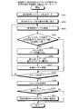
次に、図9を用いて、NANDコントローラ6aが実行する処理の流れについて説明する。図9は、NANDコントローラが実行する処理を説明する図である。例えば、NANDコントローラ6aは、図9中(A)に示すように、I/Oハブ4を介して、読出し要求や書込み要求を受信すると、読出し/書込み制御を実行する。詳細には、NANDコントローラ6aは、図9中(B)に示すように、アドレス変換テーブル19を参照して、論理アドレスと物理アドレスとのアドレス変換を実行する。 Next, the flow of processing executed by the
そして、NANDコントローラ6aは、図9中(C)に示すように、アドレス変換した物理アドレスを用いて、NANDデバイス7a〜10aに対する読出しや書込みを実行する。また、NANDコントローラ6aは、データの書込みを実行した場合は、図9中(D)に示すように、管理情報テーブル20の更新を行う。詳細には、NANDコントローラ6aは、図6中(E)に示すように、データ書込みの際に巡回回数カウンタ16がカウントしていたカウント値を管理情報テーブル20に格納する。 Then, as shown in FIG. 9C, the
また、NANDコントローラ6aは、所定の時間間隔等で、巡回参照制御を実行する。詳細には、NANDコントローラ6aは、図9中(F)に示すように、巡回回数カウンタ16の値を取得する。そして、NANDコントローラ6aは、図9中(G)に示すように、管理情報テーブル20の各エントリごとに、タイムスタンプの値と巡回回数カウンタ16の値とを比較し、データが書込まれてから所定の期間が経過したブロックを識別する。 Further, the
そして、NANDコントローラ6aは、図9中(H)に示すように、識別したブロックのデータ移動制御を実行する。例えば、NANDコントローラ6aは、図9中(I)に示すように、識別したブロックから他のブロックにデータを移動させる。そして、NANDコントローラ6aは、データの移動に従って、図9中(J)に示すように、アドレス変換テーブル19を更新し、図9中(K)に示すように、管理情報テーブル20を更新する。 Then, the
また、NANDコントローラ6aは、管理情報テーブル20の全エントリについて、タイムスタンプの値と巡回回数カウンタ16の値との比較が終了した場合は、図9中(L)に示すように、巡回回数カウンタ16の値をインクリメントする。この結果、NANDコントローラ6aは、カウンタの桁数を少ない桁数とした場合にも、カウント値が管理情報テーブル20に格納されたタイムスタンプの値を追越さないので、書込まれてから所定の期間が経過したデータの移動を行うことができる。 Further, when the comparison between the time stamp value and the value of the
次に、図10を用いて、NANDコントローラ6aが管理情報テーブル20を用いてデータ移動制御の対象となるデータを識別し、データ移動後に管理情報テーブル20を更新する例について説明する。図10は、データ移動制御を説明する図である。なお、図10に示す例では、巡回回数カウンタ16のカウント値は1桁であるものとする。 Next, an example in which the
また、図10に示す例では、NANDコントローラ6aは、タイムスタンプの値と、巡回回数カウンタ16のカウント値に「5」を加算した値とが一致する場合は、データの移動を行うものとする。また、図10に示す例では、物理ブロックアドレス「P0」が示すブロックのデータを物理ブロックアドレス「P4」が示すブロックに移動する例について説明する。 In the example shown in FIG. 10, the
例えば、NANDコントローラ6aは、巡回回数カウンタ16のカウント値が「7」の際に、物理ブロックアドレス「P1」、「P5」が示すブロックにデータを格納する。この結果、NANDコントローラ6aは、図10中(M)に示すように、物理ブロックアドレス「P1」が格納されたエントリのバリッドビットを「1」に更新し、タイムスタンプとして、巡回回数カウンタ16のカウント値「7」を格納する。また、NANDコントローラ6aは、図10中(N)に示すように、物理ブロックアドレス「P5」が格納されたエントリのバリッドビットを「1」に更新し、タイムスタンプとして、巡回回数カウンタ16のカウント値「7」を格納する。 For example, when the count value of the
ここで、巡回回数カウンタ16のカウント値「7」に「5」を加算した値は「12」であるが、桁あふれを考慮すると、加算した値は「2」となる。この結果、NANDコントローラ6aは、図10中(O)に示すように、物理ブロックアドレス「P0」が格納されたエントリのタイムスタンプが「2」であるので、物理ブロックアドレス「P0」が示すブロックのデータを移動する。また、NANDコントローラ6aは、物理ブロックアドレス「P0」が格納されたエントリのバリッドビットを「0」に更新し、タイムスタンプの値を削除する。 Here, the value obtained by adding “5” to the count value “7” of the
また、NANDコントローラ6aは、図10中(P)に示すように、データの移動先ブロックを示す物理ブロックアドレス「P4」のエントリを抽出する。そして、NANDコントローラ6aは、抽出したエントリのバリッドビットを「1」に更新し、タイムスタンプとして、巡回回数カウンタ16のカウント値「7」を格納する。その後、NANDコントローラ6aは、図10中(Q)に示すように、巡回回数カウンタ16のカウント値を「8」にインクリメントする。 Further, the
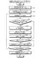
次に、図11を用いて、NANDコントローラ6aが実行する処理の流れについて説明する。図11は、実施例1に係るNANDコントローラが実行する処理の流れを説明するフローチャートである。例えば、NANDコントローラ6aは、管理情報テーブル20を参照する(ステップS101)。そして、NANDコントローラ6aは、参照した管理情報テーブル20からエントリを1つ抽出し、抽出したエントリのタイムスタンプの値が巡回回数カウンタ16のカウント値に1を加算した値か否かを判定する(ステップS102)。 Next, the flow of processing executed by the
また、NANDコントローラ6aは、タイムスタンプの値が巡回回数カウンタ16のカウント値に1を加算した値であると判定した場合は(ステップS102肯定)、以下のステップS103〜S105に示すデータ移動制御を実行する。詳細には、NANDコントローラ6aは、抽出したエントリに格納された物理ブロックアドレスが示すブロック内のデータを読み出す(ステップS103)。次に、NANDコントローラ6aは、読み出したデータを新たなブロックに書込む(ステップS104)。 If the
そして、NANDコントローラ6aは、データの移動に応じて、アドレス変換テーブル19、および、管理情報テーブル20の更新を行う(ステップS105)。なお、ステップS103〜ステップS105の処理は、リクエスト調停部13、テーブル制御部14によってアトミックに実行される。一方、NANDコントローラ6aは、タイムスタンプの値が巡回回数カウンタ16のカウント値に1を加算した値ではないと判定した場合は(ステップS102否定)、ステップS103〜S105に示すデータ移動制御をスキップする。 Then, the
また、NANDコントローラ6aは、管理情報テーブル20の全てのエントリについて、ステップS102〜S105の処理を実行したか否かを判定する(ステップS106)。そして、NANDコントローラ6aは、管理情報テーブル20の全てのエントリについて、ステップS102〜S105の処理を実行していないと判定した場合は(ステップS106否定)、以下の処理を実行する。すなわち、NANDコントローラ6aは、管理情報テーブル20の各エントリのうち、ステップS102の処理を実行していない他のエントリについてステップS102を再度実行する。 Further, the
また、NANDコントローラ6aは、管理情報テーブル20の全てのエントリについて、ステップS102〜S105の処理を実行したと判定した場合は(ステップS106肯定)、以下の処理を実行する。すなわち、NANDコントローラ6aは、巡回回数カウンタ16の値を1進め(ステップS107)、処理を終了する。 If the
[情報処理装置1の効果]
上述したように、情報処理装置1は、NANDデバイス7a〜10aが記憶するデータが移動の対象であるか判定する処理が、全てのデータに対して実行された場合は、巡回回数カウンタ16のカウント値を更新する。また、情報処理装置1は、NANDデバイス7a〜10aにデータが書込まれる際に、巡回回数カウンタ16のカウント値をデータの書込み先となるブロックの物理ブロックアドレスと対応付けて記憶する。そして、情報処理装置1は、データごとに、データが書込まれた物理ブロックアドレスと対応付けて記憶するカウント値と、巡回回数カウンタ16のカウント値とを比較して、各ブロックのデータが移動の対象であるか判定する。[Effect of information processing apparatus 1]
As described above, the
このため、情報処理装置1は、巡回回数カウンタ16のカウント値が少ない桁数であっても、管理情報テーブル20が記憶するタイムスタンプの値の追い越しを防げる。この結果、情報処理装置1は、タイムスタンプの桁数を削減することができる。また、テーブル記憶部11の記憶容量を削減できるので、NANDコントローラ6aの回路規模を小さくすることができる。また、情報処理装置1は、管理情報テーブル20のサイズを削減する結果、検索処理の時間を短縮し、NANDデバイス7a〜10aに対するアクセス性能を向上させることができる。 For this reason, the
また、情報処理装置1は、物理ブロックアドレスと、物理ブロックアドレスが示すブロックにデータを書込んだ際のカウント値であるタイムスタンプとを対応付けて管理情報テーブル20に格納する。そして、情報処理装置1は、物理ブロックアドレスごとに、巡回回数カウンタ16のカウント値と管理情報テーブル20に格納された各タイムスタンプの値とを比較して、各データを再度NANDデバイス7a〜10aに書込むか否か判定する。 Further, the
このため、情報処理装置1は、各ブロックごとに、データが書込まれてから所定の期間が経過したデータを判定できる。この結果、情報処理装置1は、NANDデバイス7a〜10aが有する各ブロックごとに、素子の劣化を平準化し、電荷が抜けることによるビット化けを防げる。 Therefore, the
また、情報処理装置1は、巡回回数カウンタ16のカウント値を所定の値で初期値に戻す。そして、情報処理装置1は、カウント値に1を加算した値と、あるデータについて管理情報テーブル20に格納されたタイムスタンプの値とが一致する場合は、データが移動の対象であると判定する。この結果、情報処理装置1は、NANDデバイス7a〜10aに格納されたデータのうち、最も古いデータの移動を行うことができる。 Further, the
上述したNANDコントローラ6aは、1回の巡回参照制御で、全ての物理ブロックアドレスについて、データの移動を行うか否か判定した。しかし、実施例はこれに限定されるものではない。例えば、実施例2に係るNANDコントローラ6cは、1回の巡回参照処理で、全ての物理ブロックアドレスのうち、一部の物理ブロックアドレスのみについて判定処理を行ってもよい。 The
以下、NANDコントローラ6cが実行する処理について説明する。まず、図12を用いて、NANDコントローラ6cの機能構成について説明する。図12は、実施例2に係るNANDコントローラの機能構成を説明する図である。なお、図12に示すNANDコントローラ6cの機能構成のうち、図6に示すNANDコントローラ6aの機能構成と同様の機能構成については、同一の符号を付し、説明を省略する。 Hereinafter, processing executed by the
図12に示す例では、NANDコントローラ6cは、巡回参照制御部17aと巡回済対象記憶部21とを有する。巡回済対象記憶部21は、巡回参照制御部17aが判定処理を行った対象を記憶するためのメモリである。巡回参照制御部17aは、図6に示す巡回参照制御部17と同様の機能を有し、所定の時間間隔で巡回参照制御を実行する。 In the example illustrated in FIG. 12, the
ここで、巡回参照制御部17aは、管理情報テーブル20の各エントリのうち、物理ブロックアドレスが「P0」のエントリから順番に判定処理を実行する。例えば、巡回参照制御部17aは、物理ブロックアドレスが「P0」のエントリを抽出し、抽出したエントリのタイムスタンプの値と巡回回数カウンタ16のカウント値とを比較し、判定処理を実行する。次に、巡回参照制御部17aは、物理ブロックアドレスが「P1」のエントリを抽出し、抽出したエントリについて判定処理を実行する。 Here, the cyclic
ここで、巡回参照制御部17aは、巡回参照制御を開始してから所定の時間が経過した場合は、最後に判定処理を実行したエントリに格納された物理ブロックアドレスを巡回済対象記憶部21に格納する。その後、巡回参照制御部17aは、巡回参照処理を再開した場合は、巡回済対象記憶部21に格納した物理ブロックアドレスの次の物理ブロックアドレスが格納されたエントリから、順番に判定処理を実行する。その後、巡回参照制御部17aは、管理情報テーブル20の全てのエントリについて判定処理を実行した場合は、巡回回数カウンタ16の値を1つインクリメントする。 Here, when a predetermined time has elapsed since the start of the cyclic reference control, the cyclic
例えば、巡回参照制御部17aは、物理ブロックアドレス「P7」のエントリについて判定処理を終了した際に、所定の時間が経過した場合は、物理ブロックアドレス「P7」を巡回済対象記憶部21に格納する。かかる場合は、巡回参照制御部17aは、巡回参照制御を再開した際に、巡回済対象記憶部21から物理ブロックアドレス「P7」を取得する。そして、巡回参照制御部17aは、管理情報テーブル20から、物理ブロックアドレス「P7」の次の物理ブロックアドレス「P8」が格納されたエントリを抽出し、抽出したエントリに対して判定処理を実行する。 For example, the cyclic
なお、巡回参照制御部17aは、所定の時間内で判別対象を区切るのではなく、他の方法で判別対象を区切ってもよい。例えば、巡回参照制御部17aは、物理ブロックアドレスを所定の数ごとにグループ分けする。そして、巡回参照制御部17aは、一回の巡回参照制御で、1つのグループに含まれる物理ブロックアドレスに対して判定処理を実行してもよい。 Note that the cyclic
例えば、巡回参照制御部17aは、物理ブロックアドレス「P0」〜「P7」をグループ「No1」とし、物理ブロックアドレス「P8」〜「P15」をグループ「No2」とする。すなわち、巡回参照制御部17aは、物理ブロックアドレスの上位ビットの値ごとに、8個の連続する物理ブロックアドレスを1つのグループとする。そして、巡回参照制御部17aは、管理情報テーブル20の各エントリのうち、グループ「No1」に含まれる物理ブロックアドレスが格納された各エントリについて判定処理を実行する。 For example, the cyclic
また、巡回参照制御部17aは、グループ「No1」に含まれる物理ブロックアドレスが格納された各エントリについて判定処理を実行した場合は、判定処理を実行したグループを示す情報として、「No1」を巡回済対象記憶部21に格納する。そして、巡回参照制御部17aは、巡回参照制御の再開時には、巡回済対象記憶部21からグループを示す情報「No1」を取得する。かかる場合は、巡回参照制御部17aは、管理情報テーブル20から、グループ「No1」の次のグループ「No2」に含まれる物理ブロックアドレスが格納された各エントリについて判定処理を実行する。 In addition, when the cyclic
なお、巡回参照制御部17aは、グループを示す情報として、任意の情報を用いることができる。例えば、巡回参照制御部17aは、物理ブロックアドレスの上位ビットでグループ分けを行う場合は、判定処理を終了したグループの物理ブロックアドレスの上位ビットを巡回済対象記憶部21に格納してもよい。 The cyclic
次に、図13を用いて、NANDコントローラ6cが実行する処理の流れについて説明する。図13は、実施例2に係るNANDコントローラが実行する処理の流れを説明する第1のフローチャートである。なお、図13に示す例では、NANDコントローラ6cが、所定の時間内で判別対象となるブロックを区切る例について記載した。また、図13に示す処理のうち、ステップS203〜ステップS207の処理については、図11に示すステップS101〜ステップS105と同様の処理であるものとして、説明を省略する。 Next, the flow of processing executed by the
まず、NANDコントローラ6cは、巡回済対象記憶部21から、前回、判定処理が終了したブロックの物理ブロックアドレスを読み出す(ステップS201)。次に、NANDコントローラ6cは、読み出した物理ブロックアドレスの次の物理ブロックアドレスが示すブロックを開始ブロックに設定する(ステップS202)。そして、NANDコントローラ6cは、ステップS203〜ステップS207の処理を実行する。 First, the
また、NANDコントローラ6cは、ステップS207を実行すると、判定対象とした物理ブロックアドレスが示すブロックが、最終ブロックであるか否かを判定する(ステップS208)。そして、NANDコントローラ6cは、判定対象とした物理ブロックアドレスが示すブロックが、最終ブロックであると判定した場合は(ステップS208肯定)、巡回回数カウンタ16のカウント値を1進める(ステップS209)。一方、NANDコントローラ6cは、判定対象とした物理ブロックアドレスが示すブロックが、最終ブロックではないと判定した場合は(ステップS208否定)、ステップS209をスキップする。 In addition, when executing step S207, the
次に、NANDコントローラ6cは、巡回参照処理を開始してから所定の時間が経過したか否かを判定する(ステップS210)。そして、NANDコントローラ6cは、巡回参照処理を開始してから所定の時間が経過したと判定した場合は(ステップS210肯定)、判定処理が終了したブロックの物理ブロックアドレスを巡回済対象記憶部21に保存し(ステップS211)、処理を終了する。一方、NANDコントローラ6cは、巡回参照処理を開始してから所定の時間が経過していないと判定した場合は(ステップS210否定)、ステップS203の処理を実行する。 Next, the
次に、図14を用いて、NANDコントローラ6cが実行する処理の他の例について説明する。図14は、実施例2に係るNANDコントローラが実行する処理の流れを説明する第2のフローチャートである。なお、図14に示す例では、NANDコントローラ6cが、物理ブロックアドレスを所定の数ごとにグループ分けし、1回の巡回参照制御で1つのグループに含まれるブロックを判定処理の対象となる例について記載した。また、図14に示す処理のうち、ステップS303〜ステップS307の処理については、図11に示すステップS101〜ステップS105と同様の判定処理であるものとして、説明を省略する。 Next, another example of processing executed by the
まず、NANDコントローラ6cは、巡回済対象記憶部21から、前回、判定処理が終了したグループのグループNoを読み出す(ステップS301)。次に、NANDコントローラ6cは、読み出したグループNoの次のグループNoが示すグループを巡回参照処理の対象に設定する(ステップS302)。そして、NANDコントローラ6cは、巡回参照処理の対象となるグループに含まれる各ブロックについて、ステップS303〜ステップS307の処理を実行する。 First, the
また、NANDコントローラ6cは、ステップS307を実行すると、判定対象とした物理ブロックアドレスが示すブロックが、巡回参照処理の対象となるグループの最終ブロックであるか判定する(ステップS308)。そして、NANDコントローラ6cは、判定対象とした物理ブロックアドレスが示すブロックが、巡回参照処理の対象となるグループの最終ブロックであると判定した場合は(ステップS308肯定)、以下の処理を実行する。すなわち、NANDコントローラ6cは、巡回参照処理の対象となるグループのグループNoを巡回済対象記憶部21に格納する(ステップS309)。 Further, when executing the step S307, the
また、NANDコントローラ6cは、巡回参照処理を実行したグループが最終グループであるか否かを判定する(ステップS310)。すなわち、NANDコントローラ6cは、管理情報テーブル20の全てのエントリについて判定処理を実行したか否かを判定する。そして、NANDコントローラ6cは、巡回参照処理を実行したグループが最終グループであると判定した場合は(ステップS310肯定)、巡回回数カウンタ16のカウント値を1進め(ステップS311)、処理を終了する。 Also, the
一方、NANDコントローラ6cは、巡回参照処理を実行したグループが最終グループではないと判定した場合は(ステップS310否定)、ステップS311をスキップして処理を終了する。また、NANDコントローラ6cは、判定対象とした物理ブロックアドレスが示すブロックが、巡回参照処理の対象となるグループの最終ブロックではないと判定した場合は(ステップS308否定)、ステップS303の処理を実行する。 On the other hand, if the
[NANDコントローラ6cの効果]
上述したように、NANDコントローラ6cは、巡回参照制御を開始してから所定の時間が経過した場合は、最後に判定処理の対象となったブロックの物理ブロックアドレスを記憶する。その後、NANDコントローラ6cは、巡回参照処理の再開時には、記憶した物理ブロックアドレスの次の物理ブロックアドレスが示すブロックから、物理ブロックアドレスの順で、巡回参照処理を実行する。[Effect of
As described above, the
このため、NANDコントローラ6cは、巡回参照処理を1回実行する際の処理時間を短縮することができる。この結果、NANDコントローラ6cは、例えば、情報処理装置1が処理を実行していない夜間等に、巡回参照処理を実行する等、柔軟なスケジューリングを実現することができる。また、NANDコントローラ6cは、巡回参照処理によってNANDデバイス7a〜10aにアクセスできない時間を短縮化するので、NANDデバイス7a〜10aに対するアクセス性能を向上させることができる。 For this reason, the
また、NANDコントローラ6cは、NANDデバイス7a〜10aの記憶領域を複数のグループに分割し、グループごとに、巡回参照処理を実行する。このため、NANDコントローラ6cは、巡回参照処理を1回実行する際の処理時間を短縮し、柔軟なスケジューリングを実現できる。また、NANDコントローラ6cは、NANDデバイス7a〜10aに対するアクセス性能を向上させることができる。 The
上述したNANDコントローラ6a〜6cは、巡回回数カウンタ16のカウント値に所定の閾値を加算した値と、タイムスタンプの値とが一致した場合は、データの移動処理を実行した。しかし、実施例は、これに限定されるものではない。例えば、NANDコントローラ6a〜6cは、各ブロックに対するリクエストの数に応じて、閾値を動的に設定してもよい。 The
以下、実施例3に係るNANDコントローラとして、各ブロックに対するリクエストの数に応じて、異なる閾値を設定するNANDコントローラ6dについて説明する。まず、図15を用いて、NANDコントローラ6dの機能構成について説明する。図15は、実施例3に係るNANDコントローラの機能構成を説明する図である。なお、図15に示すNANDコントローラ6dの機能構成のうち、図6に示すNANDコントローラ6aの機能構成と同様の機能構成については、同一の符号を付し、説明を省略する。 A NAND controller 6d that sets different thresholds according to the number of requests for each block will be described below as a NAND controller according to the third embodiment. First, the functional configuration of the NAND controller 6d will be described with reference to FIG. FIG. 15 is a diagram illustrating a functional configuration of the NAND controller according to the third embodiment. Of the functional configuration of the NAND controller 6d shown in FIG. 15, the same functional configuration as that of the
例えば、NANDコントローラ6dは、巡回参照制御部17bと、リクエスト数計測部22とを有する。リクエスト数計測部22は、NANDデバイス7a〜10aが有するブロックごとに、以下の処理を実行する。まず、リクエスト数計測部22は、リクエスト調停部13とテーブル制御部14とを接続する信号線やバスを監視し、各ブロックに対して発行されたリクエストの数を計数する。詳細には、リクエスト数計測部22は、所定の時間間隔で、各ブロックに対して発行されたリクエストの数、例えば、読出し要求や書込み要求の数をブロックごとに計測する。 For example, the NAND controller 6 d includes a cyclic
なお、リクエスト数計測部22は、読出し要求、又は、書込み要求のいずれか一方の数を計数してもよい。また、リクエスト数計測部22は、リクエスト調停部13とデバイスアクセス制御部15とを接続する信号線やバスを監視することで、各ブロックに対するリクエストの数を計数しても良い。 Note that the request
また、リクエスト数計測部22は、計測結果から、10秒間に発行されたリクエストの平均値である平均要求発行数をブロックごとに算出する。そして、リクエスト数計測部22は、算出した平均要求発行数に応じた閾値をブロックごとに設定する。その後、リクエスト数計測部22は、ブロックごとに設定した閾値を巡回参照制御部17bに出力する。なお、リクエスト数計数部22は、特許請求の範囲に記載の要求計数部、および、設定部の一例である。 Moreover, the request
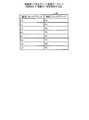
ここで、図16を用いて、リクエスト数計測部22が、平均要求発行数に応じて設定する閾値の一例について説明する。図16は、平均要求発行数に応じた閾値の一例を説明する図である。例えば、図16に示すように、リクエスト数計測部22は、平均要求発行数が「0」から「9」の間であるブロックの閾値を「4」とし、平均要求発行数が「10」から「49」の間であるブロックの閾値を「3」とする。 Here, an example of the threshold set by the request
また、リクエスト数計測部22は、平均要求発行数が「50」から「99」の間であるブロックの閾値を「2」とし、平均要求発行数が「100」以上であるブロックの閾値を「1」とする。なお、図16に示す平均要求発行数と閾値との対応は、あくまで一例であり、NANDコントローラ6dは、平均要求発行数の数に応じた閾値を設定するのであれば、任意の閾値を設定できる。 Further, the request
図15に戻り、巡回参照制御部17bは、図6に示す巡回参照制御部17と同様の機能を発揮する。また、巡回参照制御部17bは、管理情報テーブル20の各エントリについて、判定処理を実行する場合は、以下の処理を実行する。まず、巡回参照制御部17bは、管理情報テーブル20から判定処理の対象となるエントリを抽出する。 Returning to FIG. 15, the cyclic
また、巡回参照制御部17bは、抽出したエントリに格納された物理ブロックアドレスが示すブロックに対してリクエスト数計測部22が設定した閾値と、現在の巡回回数カウンタ16のカウント値との和の値を算出する。そして、巡回参照制御部17bは、抽出したエントリに格納されたタイムスタンプの値が算出した和の値以下となるか否かを判定する。 In addition, the cyclic
また、巡回参照制御部17bは、抽出したエントリに格納されたタイムスタンプの値が算出した和の値以下となる場合は、抽出したエントリに格納された物理ブロックアドレスをデータ移動制御部18に出力し、データを移動させる。一方、巡回参照制御部17bは、抽出したエントリに格納されたタイムスタンプの値が算出した和の値より大きい場合は、データを移動させずに、管理情報テーブル20の次のエントリについて判定処理を実行する。 The cyclic
この結果、NANDコントローラ6dは、読出し要求や書込み要求が頻繁に発行されるブロックについては、データの移動を先延ばしするので、読出し要求や書込み要求が阻害されずに実行される結果、アクセス性能の悪化を防ぐことができる。一方、NANDコントローラ6dは、読出し要求や書込み要求があまり発行されていないブロックについては、データの移動を前倒しで実行するので、アクセス性能の悪化を防ぎつつ、ビット化けを防ぐことができる。 As a result, since the NAND controller 6d postpones the movement of data for a block in which read requests and write requests are frequently issued, the read request and write request are executed without being obstructed, resulting in an increase in access performance. Deterioration can be prevented. On the other hand, since the NAND controller 6d executes data movement ahead of time for blocks for which read requests and write requests are not issued much, it can prevent bit corruption while preventing deterioration in access performance.
次に、図17を用いて、NANDコントローラ6dが実行する処理の他の例について説明する。図17は、実施例3に係るNANDコントローラが実行する処理の流れを説明するフローチャートである。また、図17に示す処理のうち、ステップS401、ステップS403〜ステップS407の処理については、図11に示すステップS101、ステップS103〜ステップS107と同様の判定処理であるものとして、説明を省略する。 Next, another example of processing executed by the NAND controller 6d will be described with reference to FIG. FIG. 17 is a flowchart illustrating the flow of processing executed by the NAND controller according to the third embodiment. In addition, among the processes shown in FIG. 17, the processes in steps S401 and S403 to S407 are the same as the determination processes in steps S101 and S103 to S107 shown in FIG.
例えば、NANDコントローラ6dは、判定処理の対象となるエントリについて、巡回回数カウンタ16のカウント値に平均要求発行数に応じた閾値を加算した値がタイムスタンプの値以上か否かを判定する(ステップS402)。そして、NANDコントローラ6dは、巡回回数カウンタ16のカウント値に平均要求発行数に応じた閾値を加算した値がタイムスタンプの値以上である場合は(ステップS402肯定)、ステップS403の処理を実行する。一方、NANDコントローラ6dは、巡回回数カウンタ16のカウント値に平均要求発行数に応じた閾値を加算した値がタイムスタンプの値より少ない場合は(ステップS402否定)、ステップS406を実行する。 For example, the NAND controller 6d determines whether or not a value obtained by adding a threshold corresponding to the average number of issued requests to the count value of the
[NANDコントローラ6dの効果]
上述したように、NANDコントローラ6dは、ブロックごとに、発行された読出し要求、および、書込み要求の数を計数する。また、NANDコントローラ6dは、計数した数に応じて、各ブロックのデータを移動させるか否かを判定するための閾値、すなわち、各ブロックのデータが移動の対象であるか判定するための閾値をブロックごとに設定する。[Effect of NAND controller 6d]
As described above, the NAND controller 6d counts the number of issued read requests and write requests for each block. In addition, the NAND controller 6d sets a threshold value for determining whether or not to move the data of each block according to the counted number, that is, a threshold value for determining whether or not the data of each block is a movement target. Set for each block.
そして、NANDコントローラ6dは、ブロックごとに、巡回回数カウンタ16のカウント値と設定した閾値との和を算出し、算出した値が管理情報テーブル20に格納されたタイムスタンプの値以上となるか否かを判定する。その後、NANDコントローラ6dは、算出した値が管理情報テーブル20に格納されたタイムスタンプの値以上となる場合は、判断対象のブロックに格納されたデータが移動の対象であると判定する。 Then, the NAND controller 6d calculates the sum of the count value of the
このため、NANDコントローラ6dは、CPU3a、3bが発行するリクエストの数に応じて、データの移動のを行うことができる。例えば、NANDコントローラ6dは、読出し要求や書込み要求が頻繁に発行されるブロックについては、データの移動を先延ばし、読出し要求や書込み要求があまり発行されていないブロックについては、データの移動を前倒しして実行する。この結果、NANDコントローラ6dは、アクセス性能の悪化や、ビット化けを防ぐことができる。 Therefore, the NAND controller 6d can move data according to the number of requests issued by the CPUs 3a and 3b. For example, the NAND controller 6d defers data movement for a block in which read requests and write requests are frequently issued, and advances data movement for a block in which read requests and write requests are not issued frequently. And execute. As a result, the NAND controller 6d can prevent deterioration in access performance and bit corruption.
これまで本発明の実施例について説明したが実施例は、上述した実施例以外にも様々な異なる形態にて実施されてよいものである。そこで、以下では実施例4として本発明に含まれる他の実施例を説明する。 Although the embodiments of the present invention have been described so far, the embodiments may be implemented in various different forms other than the embodiments described above. Accordingly, another embodiment included in the present invention will be described below as a fourth embodiment.
(1)データ移動の粒度について
上述したNANDコントローラ6a〜6dは、NANDデバイス7a〜10aが有するブロックごとに、データを移動させるか否かを判定した。しかしながら、実施例はこれに限定されるものではない。すなわち、NANDコントローラ6a〜6dは、任意の単位でデータの移動を行うか否かを判定することができる。例えば、NANDコントローラ6a〜6dは、複数のブロックごとにデータの移動を行うか否かを判定してもよい。また、NANDコントローラ6a〜6dは、管理情報テーブル20がタイムスタンプを管理する単位と、データ書込みの単位とに異なる粒度を採用してもよい。(1) Granularity of data movement The
(2)NANDコントローラ6a〜6dの機能構成について
上述したNANDコントローラ6a〜6dの機能構成は、あくまで一例であり、NANDコントローラ6a〜6dとして同様の処理を実行できるのであれば、任意の構成を採用することができる。例えば、NANDコントローラ6aは、巡回参照制御部17とデータ移動制御部18との機能を有する移動制御部を有してもよい。(2) Regarding the functional configuration of the
なお、上述した例では、NANDコントローラ6a〜6dがNANDデバイス7a〜10aに格納されたデータの移動を判定する処理について記載した。しかしながら、実施例はこれに限定されるものではない。すなわち、NANDコントローラ6a〜6dは、データの移動のを行うのであれば、任意の技術が適用された記憶媒体、例えばメモリ等のメモリコントローラとして動作してもよい。 In the example described above, the
(3)リクエストの調停について
上述したNANDコントローラ6a〜6dは、リクエスタインターフェース部12から受信する読出し要求や書込み要求を優先して実行した。しかし、実施例はこれに限定されるものではなく、NANDコントローラ6a〜6dは、NANDデバイス7a〜10aの各セルの寿命が平準化するように、各リクエストの調停を行ってもよい。(3) Request Arbitration
(4)予備ブロックについて
上述したテーブル制御部14は、データが格納されていない予備ブロックをデータの移動先とした。しかしながら、実施例はこれに限定されるものではない。例えば、テーブル制御部14は、データが格納されていないブロックのうち、最も余命が長いブロックを識別する。そして、テーブル制御部14は、識別したブロックを示す物理ブロックアドレスをリクエスト調停部13に通知してもよい。かかる処理を実行した場合は、NANDコントローラ6a〜6dは、NANDデバイス7a〜10aが有する各ブロックのセルの劣化を平準化し、寿命を使いきることができる。(4) Spare Block The
(5)巡回回数カウンタについて
上述したNANDコントローラ6a〜6dは、「0」から「9」までカウントする巡回回数カウンタ16を有する。しかしながら、実施例はこれに限定されるものではない。すなわち、巡回回数カウンタ16がカウントする値は、任意の範囲や桁数を設定することができる。例えば、NANDコントローラ6a〜6dは、「0」または「1」をカウントする巡回回数カウンタ16を有し、2回の巡回参照制御で全てのデータを移動させてもよい。(5) Cyclic Count Counter The
また、NANDコントローラ6a〜6dは、カウンタを巡回回数カウンタ16として有する必要はない。例えば、NANDコントローラ6a〜6dは、所定の桁数の数値を記憶可能なメモリを有し、メモリ上にカウント値を格納する。そして、NANDコントローラ6a〜6dは、管理情報テーブル20の全てのエントリについて判定処理を完了した場合は、メモリ上のカウント値を読出し、読み出した値に1を加算した値を再度メモリに書込むことで、巡回回数カウンタ16を再現してもよい。 Further, the
なお、NANDコントローラ6a〜6dは、任意の記憶装置に巡回参照制御を実行した回数を格納し、巡回参照制御を実行後に、記憶装置に格納した回数を更新することで、巡回回数カウンタ16の機能を実現してもよい。 The
また、NANDコントローラ6a〜6dは、各ブロックごとに、巡回参照制御を行った後でデータの書込みが行われたか否かを示す書込ビットを管理情報テーブル20に格納する。そして、NANDコントローラ6a〜6dは、管理情報テーブル20の書込ビットを参照し、巡回参照制御を行った後でデータの書込みが行われなかったブロックを識別する。その後、NANDコントローラ6a〜6dは、識別したブロックのデータを移動させ、管理情報テーブル20のフラグをリセットしてもよい。 The
すなわち、NANDコントローラ6a〜6dは、前回巡回参照処理を行ってから書込みが行われなかったブロックについて、データの再書込を行う場合は、巡回回数カウンタ16を有さず、書込ビットを用いて処理を行っても良い。以下、図18を用いて、NANDコントローラ6aが巡回回数カウンタ16を用いずに、巡回参照処理を実行する処理の一例について説明する。 That is, the
図18は、書込ビットを用いた処理の一例を説明する図である。なお、図18に示す例では、NANDコントローラ6aが、巡回回数カウンタ16を用いずに巡回参照処理を実行する際に、管理情報テーブル20に格納する情報について記載した。図18に示すように、NANDコントローラ6aは、管理情報テーブル20に、タイムスタンプに変えて書込ビットを格納する。ここで、書込ビットとは、前回巡回参照処理が実行されてから、データの書込みや移動が行われたか否かを示す情報である。 FIG. 18 is a diagram illustrating an example of processing using a write bit. In the example illustrated in FIG. 18, the information stored in the management information table 20 when the
例えば、図18に示す例では、管理情報テーブル20は、物理ブロックアドレス「P0」、「P5」が示すブロックにデータが格納されている旨を示す。ここで、NANDコントローラ6aは、データの更新や移動を行った結果、物理ブロックアドレス「P5」が示すブロックに格納されたデータを物理ブロックアドレス「P1」が示すブロックに移動する。 For example, in the example shown in FIG. 18, the management information table 20 indicates that data is stored in the blocks indicated by the physical block addresses “P0” and “P5”. Here, as a result of updating or moving the data, the
そして、NANDコントローラ6aは、管理情報テーブル20の各エントリのうち、物理ブロックアドレス「P5」のバリッドビットを「0」に更新し、物理ブロックアドレス「P1」のバリッドビットを「1」に更新する。また、NANDコントローラ6aは、図18中(R)に示すように、物理ブロックアドレス「P1」の書込ビットを「1」に更新する。 Then, the
ここで、NANDコントローラ6aは、巡回参照処理を実行する場合は、以下の処理を実行する。まず、NANDコントローラ6aは、管理情報テーブル20の各エントリのうち、バリッドビットが「1」で書込ビットが「0」のエントリを識別する。すなわち、NANDコントローラ6aは、前回巡回参照処理が実行された後で書込みや移動が行われたブロックの物理ブロックアドレスを識別する。そして、NANDコントローラ6aは、識別した物理ブロックアドレスが示すブロックのデータを他のブロックに移動する。 Here, when executing the cyclic reference process, the
例えば、NANDコントローラ6aは、図18に示す管理情報テーブル20から、バリッドビットが「1」で書込みビットが「0」のエントリに格納された物理ブロックアドレス「P0」を識別する。そして、NANDコントローラ6aは、図18中(S)に示すように、物理ブロックアドレス「P0」が示すブロックのデータを物理ブロックアドレス「P2」が示すブロックに移動させ、管理情報テーブル20を更新する。また、NANDコントローラ6aは、管理情報テーブル20の全エントリについて、上述した処理を実行し、全エントリについて処理が終了した場合は、管理情報テーブル20に格納された全ての書込みビットを「0」にリセットする。 For example, the
この結果、NANDコントローラ6aは、カウンタを用いずとも、書込みから所定の期間が経過したデータを移動させることができるので、管理情報テーブル20のデータ量を削減できる。なお、NANDコントローラ6aは、データの移動を行った際に書込ビットの値を「1」に更新し、全エントリについて処理が終了した場合は、管理情報テーブル20に格納された全ての書込ビットを「0」にリセットしなくともよい。かかる場合は、NANDコントローラ6aは、任意のタイミングで、書込ビットのリセットを行えばよい。 As a result, the
(6)リクエスト数計測の粒度について
上述したNANDコントローラ6dは、各ブロックに対して発行されたリクエストの数をリクエスト数計測部22がブロックごとに計測し、ブロックごとに閾値を設定した。しかし、実施例はこれに限定されるものではなく、NANDコントローラ6dは、異なる粒度でリクエスト数の計測と閾値の設定を行ってもよい。例えば、NANDコントローラ6dは、すべてのブロックに対して発行されたリクエストを共通のカウンタで計測し、NANDコントローラ6d全体で共通の閾値を1つ設定してもよい。また、NANDコントローラ6dは、複数のブロックを含むグループごとに、リクエストが発行された数に応じた閾値を設定してもよい。(6) Granularity of Request Count Measurement In the NAND controller 6d described above, the request
このように、NANDコントローラ6dは、すべてのブロックに対して発行されたリクエストの数に応じて、データの移動を判定する閾値を設定した場合は、例えば、読出しや書込みが頻繁に発行される場合は、データの移動を先延ばしできる。また、NANDコントローラ6dは、読出し要求や書込み要求があまり発行されていない場合は、データの移動を前倒しして実行できる。この結果、NANDコントローラ6dは、アクセス性能の悪化や、ビット化けを防ぐことができる。 As described above, when the threshold value for determining data movement is set according to the number of requests issued to all blocks, the NAND controller 6d, for example, when reading and writing are frequently issued Can postpone data movement. Further, the NAND controller 6d can execute data movement ahead of schedule when there are not many read requests or write requests issued. As a result, the NAND controller 6d can prevent deterioration in access performance and bit corruption.
(7)プログラム
上記の実施例で説明したNANDコントローラ6a〜6dが発揮する機能は、予め用意された制御プログラムをNANDコントローラ内の演算処理装置が実行することで実現してもよい。そこで、以下では、図19を用いて、上記のNANDコントローラ6aと同様の機能を有する制御プログラムを実行するコンピュータの一例について説明する。(7) Program The functions exhibited by the
図19は、制御プログラムを実行するNANDコントローラの一例を説明する図である。図19に示すように、NANDコントローラ6eは、CPU40、デバイスアクセス制御部15を有する。また、CPU40は、メモリデバイス11aと接続される。なお、メモリデバイス11aは、NANDコントローラ6eに内蔵されるメモリであってもよい。 FIG. 19 is a diagram illustrating an example of a NAND controller that executes a control program. As illustrated in FIG. 19, the NAND controller 6 e includes a
メモリデバイス11aには、巡回回数カウンタ16、アドレス変換テーブル19、管理情報テーブル20があらかじめ記憶される。ここで、CPU40が制御プログラム30を
読出して展開して実行することにより、制御プログラム30は、以下の様に機能する。すなわち、制御プログラム30は、CPU40をテーブル制御部31、リクエスト調停部32、巡回参照制御部33、データ移動制御部34として動作させる。ここで、テーブル制御部31、リクエスト調停部32、巡回参照制御部33、データ移動制御部34は、図6に示すテーブル制御部14、リクエスト調停部13、巡回参照制御部17、データ移動制御部18と同様の機能を発揮する。In the
なお、上記の制御プログラム30は、CPU40に、巡回参照制御の実行回数を巡回回数カウンタ16としてメモリデバイス11a上に格納させる。そして、制御プログラム30は、CPU40に、全てのブロックに対して巡回参照制御を実行させた場合は、巡回回数カウンタ16の値を更新させる。また、NANDコントローラ6eは、CPUではなく、例えばMPUやFPGA等の演算装置を用いて制御プログラム30を実行しても良い。 The
また、上記の制御プログラム30については、例えば、メモリデバイス11aや、NANDデバイス7a〜10aに記憶させてもよいし、他の方法でCPU40に実行させてもよい。例えば、フレキシブルディスク、いわゆるFD(Flexible Disk)、CD(Compact Disk)−ROM、DVD(Digital Versatile Disk)、光磁気ディスク、ICカードなどの「可搬用の物理媒体」に各プログラムを記憶させる。 Further, the
そして、NANDコントローラ6eが各CPU3a、3bを介して、これらの可搬用の物理媒体から各プログラムを取得して実行するようにしてもよい。また、公衆回線、インターネット、LAN、WAN(Wide Area Network)などを介して他のコンピュータまたはサーバ装置などに記憶させた各プログラムを取得して実行するようにしてもよい。 Then, the NAND controller 6e may acquire and execute each program from these portable physical media via the CPUs 3a and 3b. Further, each program stored in another computer or a server device may be acquired and executed via a public line, the Internet, a LAN, a WAN (Wide Area Network), or the like.
1 情報処理装置
2a、2b メモリ
3a、3b、40 CPU
4 I/Oハブ
5a、5b SSD
6a〜6e NANDコントローラ
7a〜10a、7b〜10b NANDデバイス
11 テーブル記憶部
12 リクエスタインターフェース部
13、32 リクエスト調停部
14、31 テーブル制御部
15 デバイスアクセス制御部
16 巡回回数カウンタ
17、33 巡回参照制御部
18、34 データ移動制御部
19 アドレス変換テーブル
20 管理情報テーブル
21 巡回済対象記憶部
22 リクエスト数計測部
30 制御プログラム1
4 I /
6a to 6e
Claims (9)
Translated fromJapanese前記記憶装置が有する複数の記憶領域の各々に記憶されたデータが移動の対象であるか判定する処理が、前記記憶装置が記憶する全てのデータに対して実行されるとカウント値を更新する計数部と、
前記記憶装置にデータが書込まれる際に、前記計数部のカウント値を前記データと対応付けて記憶する計数値記憶部と、
前記記憶装置が記憶するデータごとに、前記計数値記憶部が記憶する値と前記計数部のカウント値とを比較して、各データが移動の対象であるか判定する判定部と、
前記記憶装置に対して発行されたデータの読出し要求、または、前記記憶装置に対して発行されたデータの書込み要求の数を計数する要求計数部と、
前記要求計数部が計数した前記読出し要求の数、または、前記書込み要求の数に応じて、前記データが移動の対象であるか判定するための閾値を設定する設定部と、
を有し、
前記判定部は、前記計数部のカウント値に前記設定部が設定した閾値を加算した値が、前記計数値記憶部が記憶する値以上となる場合は、当該値と対応付けて前記計数値記憶部が記憶するデータが移動の対象であると判定する、
ことを特徴とする情報処理装置。A storage device;
Count that updates the count value when the process of determining whether the data stored in each of the plurality of storage areas of the storage device is the object of movement is executed for all the data stored in the storage device And
A count value storage unit that stores the count value of the counting unit in association with the data when data is written to the storage device;
For each data stored in the storage device, a determination unit that compares the value stored in the count value storage unit with the count value of the counting unit to determine whether each data is a target of movement;
A request counter for counting the number of data read requests issued to the storage device or the number of data write requests issued to the storage device;
A setting unit that sets a threshold for determining whether the data is a target of movement according to the number of read requests counted by the request counting unit or the number of write requests;
Have
When the value obtained by adding the threshold set by the setting unit to the count value of the counting unit is equal to or greater than the value stored in the count value storage unit, the determination unit stores the count value in association with the value. Determine that the data stored in the part is the object of movement,
An information processing apparatus characterized by that.
前記判定部は、前記領域識別子ごとに、前記計数値記憶部が記憶する値と前記計数部のカウント値とを比較して、前記領域識別子が示す記憶領域に書込まれたデータが移動の対象であるか判定することを特徴とする請求項1に記載の情報処理装置。The count value storage unit stores a count value of the count unit in association with the data when data is written in a storage area indicated by the area identifier and the storage area indicated by the area identifier,
For each region identifier, the determination unit compares the value stored in the count value storage unit with the count value of the counter unit, and the data written in the storage region indicated by the region identifier is the object of movement. The information processing apparatus according to claim 1, wherein the information processing apparatus determines whether or not.
前記判定部は、前記計数部のカウント値に1を加算した値と、前記計数値記憶部が記憶する値とが一致する場合は、当該値と対応付けられたデータが移動の対象であると判定することを特徴とする請求項1〜4のいずれか1つに記載の情報処理装置。When the count value becomes a predetermined value as a result of the update, the counting unit returns the count value to an initial value,
When the value obtained by adding 1 to the count value of the counting unit matches the value stored in the count value storage unit, the determination unit determines that the data associated with the value is a target of movement. The information processing device according to claim 1, wherein the information processing device is determined.
前記設定部は、前記要求計数部が計数した前記読出し要求の数、または、前記書込み要求の数に応じて、前記閾値を前記記憶領域ごとに設定し、
前記判定部は、前記記憶装置が有する記憶領域ごとに、前記設定部が設定した閾値と前記計数部のカウント値とを加算した値が、前記記憶領域に書込まれたデータと対応付けて前記計数値記憶部が記憶する値以上となる場合は、前記記憶領域に書込まれたデータが移動の対象であると判定することを特徴とする請求項1〜5のいずれか1つに記載の情報処理装置。The request counting unit counts the number of read requests issued or the number of write requests issued for each storage area,
The setting unit sets the threshold for each storage area according to the number of read requests counted by the request counting unit or the number of write requests.
For each storage area of the storage device, the determination unit adds a threshold value set by the setting unit and a count value of the counting unit in association with data written in the storage area. If the count storage unit is equal to or greater than the value to be stored is according toany one of claims1 to5, characterized in that data written in the storage area is determined to be the movement of the object Information processing device.
前記記憶装置にデータが書込まれる際に、前記計数部のカウント値を前記データと対応付けて記憶する計数値記憶部と、
前記記憶装置が記憶するデータごとに、前記計数値記憶部が記憶する値と前記計数部のカウント値とを比較して、各データが移動の対象であるか判定する判定部と、
前記記憶装置に対して発行されたデータの読出し要求、または、前記記憶装置に対して発行されたデータの書込み要求の数を計数する要求計数部と、
前記要求計数部が計数した前記読出し要求の数、または、前記書込み要求の数に応じて、前記データが移動の対象であるか判定するための閾値を設定する設定部と、
を有し、
前記判定部は、前記計数部のカウント値に前記設定部が設定した閾値を加算した値が、前記計数値記憶部が記憶する値以上となる場合は、当該値と対応付けて前記計数値記憶部が記憶するデータが移動の対象であると判定する、
ことを特徴とする前記記憶装置の制御回路。A counting unit that updates the count value when the process of determining whether the data stored in each of the plurality of storage areas of the storage device is the object of movement is executed for all the data stored in the storage device When,
A count value storage unit that stores the count value of the counting unit in association with the data when data is written to the storage device;
For each data stored in the storage device, a determination unit that compares the value stored in the count value storage unit with the count value of the counting unit to determine whether each data is a target of movement;
A request counter for counting the number of data read requests issued to the storage device or the number of data write requests issued to the storage device;
A setting unit that sets a threshold for determining whether the data is a target of movement according to the number of read requests counted by the request counting unit or the number of write requests;
Have
When the value obtained by adding the threshold set by the setting unit to the count value of the counting unit is equal to or greater than the value stored in the count value storage unit, the determination unit stores the count value in association with the value. Determine that the data stored in the part is the object of movement,
A control circuit for the storage device.
記憶装置が有する複数の記憶領域の各々に記憶されたデータが移動の対象であるか判定する処理が、前記記憶装置が記憶する全てのデータに対して実行されるとカウント値を更新し、
前記記憶装置にデータが書込まれる際に、カウント値と前記データとを対応付けて所定の記憶部に記憶し、
前記記憶装置が記憶するデータごとに、前記所定の記憶部が記憶する値と前記カウント値とを比較して、各データが移動の対象であるか判定し、
前記記憶装置に対して発行されたデータの読出し要求、または、前記記憶装置に対して発行されたデータの書込み要求の数を計数し、
計数した前記読出し要求の数、または、前記書込み要求の数に応じて、前記データが移動の対象であるか判定するための閾値を設定する、各処理を実行させ、
前記判定する処理は、前記計数する処理のカウント値に前記設定する処理が設定した閾値を加算した値が、前記記憶する処理が記憶する値以上となる場合は、当該値と対応付けて前記記憶する処理が記憶するデータが移動の対象であると判定する、
ことを特徴とする制御プログラム。On the computer,
When the process of determining whether the data stored in each of the plurality of storage areas of the storage device is the object of movement is executed for all the data stored in the storage device, the count value is updated,
When data is written to the storage device, the count value and the data are associated with each other and stored in a predetermined storage unit,
For each data stored in the storage device, the value stored in the predetermined storage unit is compared with the count value to determine whether each data is a target of movement,
Count the number of data read requests issued to the storage device or data write requests issued to the storage device,
Depending on the number of read requests counted or the number of write requests, a threshold for determining whether the data is an object of movement is set to execute each process,
If the value obtained by adding the threshold value set by the setting process to the count value of the counting process is equal to or greater than the value stored by the storing process, the determining process associates the value with the value. Determining that the data stored by the process to be moved is the object of movement,
A control program characterized by that.
記憶装置が有する複数の記憶領域の各々に記憶されたデータが移動の対象であるか判定する処理が、前記記憶装置が記憶する全てのデータに対して実行されるとカウント値を更新し、
前記記憶装置にデータが書込まれる際に、カウント値と前記データとを対応付けて所定の記憶部に記憶し、
前記記憶装置が記憶するデータごとに、前記所定の記憶部が記憶する値と前記カウント値とを比較して、各データが移動の対象であるか判定し、
前記記憶装置に対して発行されたデータの読出し要求、または、前記記憶装置に対して発行されたデータの書込み要求の数を計数し、
計数した前記読出し要求の数、または、前記書込み要求の数に応じて、前記データが移動の対象であるか判定するための閾値を設定する、各処理を実行し、
前記判定する処理は、前記計数する処理のカウント値に前記設定する処理が設定した閾値を加算した値が、前記記憶する処理が記憶する値以上となる場合は、当該値と対応付けて前記記憶する処理が記憶するデータが移動の対象であると判定する、
ことを特徴とする前記記憶装置の制御方法。Information processing device
When the process of determining whether the data stored in each of the plurality of storage areas of the storage device is the object of movement is executed for all the data stored in the storage device, the count value is updated,
When data is written to the storage device, the count value and the data are associated with each other and stored in a predetermined storage unit,
For each data stored in the storage device, the value stored in the predetermined storage unit is compared with the count value to determine whether each data is a target of movement,
Count the number of data read requests issued to the storage device or data write requests issued to the storage device,
Depending on the number of read requests counted or the number of write requests, a threshold for determining whether the data is a target of movement is executed,
If the value obtained by adding the threshold value set by the setting process to the count value of the counting process is equal to or greater than the value stored by the storing process, the determining process associates the value with the value. Determining that the data stored by the process to be moved is the object of movement,
A method for controlling the storage device.
Priority Applications (3)
| Application Number | Priority Date | Filing Date | Title |
|---|---|---|---|
| JP2013096046AJP6167646B2 (en) | 2013-04-30 | 2013-04-30 | Information processing apparatus, control circuit, control program, and control method |
| US14/228,655US20140325123A1 (en) | 2013-04-30 | 2014-03-28 | Information processing apparatus, control circuit, and control method |
| EP20140162321EP2799996A1 (en) | 2013-04-30 | 2014-03-28 | Information processing apparatus, control circuit, control program, and control method |
Applications Claiming Priority (1)
| Application Number | Priority Date | Filing Date | Title |
|---|---|---|---|
| JP2013096046AJP6167646B2 (en) | 2013-04-30 | 2013-04-30 | Information processing apparatus, control circuit, control program, and control method |
Publications (2)
| Publication Number | Publication Date |
|---|---|
| JP2014220021A JP2014220021A (en) | 2014-11-20 |
| JP6167646B2true JP6167646B2 (en) | 2017-07-26 |
Family
ID=50624377
Family Applications (1)
| Application Number | Title | Priority Date | Filing Date |
|---|---|---|---|
| JP2013096046AExpired - Fee RelatedJP6167646B2 (en) | 2013-04-30 | 2013-04-30 | Information processing apparatus, control circuit, control program, and control method |
Country Status (3)
| Country | Link |
|---|---|
| US (1) | US20140325123A1 (en) |
| EP (1) | EP2799996A1 (en) |
| JP (1) | JP6167646B2 (en) |
Families Citing this family (7)
| Publication number | Priority date | Publication date | Assignee | Title |
|---|---|---|---|---|
| KR102292172B1 (en)* | 2014-06-23 | 2021-08-25 | 삼성전자주식회사 | Nonvolatile memory system and operating method of memory controller |
| CN106469126B (en)* | 2015-08-12 | 2020-07-07 | 北京忆恒创源科技有限公司 | Method for processing IO request and storage controller thereof |
| US10162526B2 (en) | 2015-10-20 | 2018-12-25 | Micron Technology, Inc. | Logical address history management in memory device |
| CN110928737B (en)* | 2018-09-19 | 2021-05-18 | 华为技术有限公司 | Method and apparatus for monitoring memory access behavior of sample process |
| US11023172B2 (en)* | 2019-07-26 | 2021-06-01 | Micron Technology, Inc. | Selecting read voltage using write transaction data |
| KR102691952B1 (en)* | 2019-10-14 | 2024-08-06 | 에스케이하이닉스 주식회사 | Controller and data storage system having the same |
| CN114168077A (en)* | 2021-12-07 | 2022-03-11 | 深圳忆联信息系统有限公司 | Timestamp management method and device for solid state disk, computer equipment and storage medium |
Family Cites Families (17)
| Publication number | Priority date | Publication date | Assignee | Title |
|---|---|---|---|---|
| JP3251968B2 (en) | 1992-01-20 | 2002-01-28 | 富士通株式会社 | Semiconductor storage device |
| JP3412839B2 (en)* | 1992-07-01 | 2003-06-03 | 株式会社東芝 | Nonvolatile semiconductor memory device |
| JPH08147988A (en) | 1994-11-17 | 1996-06-07 | Sony Corp | Semiconductor nonvolatile storage |
| US7012835B2 (en)* | 2003-10-03 | 2006-03-14 | Sandisk Corporation | Flash memory data correction and scrub techniques |
| US7173852B2 (en)* | 2003-10-03 | 2007-02-06 | Sandisk Corporation | Corrected data storage and handling methods |
| JP4643315B2 (en) | 2005-03-11 | 2011-03-02 | 株式会社東芝 | Semiconductor integrated circuit device |
| JP4366420B2 (en)* | 2007-10-30 | 2009-11-18 | Tdk株式会社 | MEMORY CONTROLLER, FLASH MEMORY SYSTEM HAVING MEMORY CONTROLLER, AND FLASH MEMORY CONTROL METHOD |
| US8239612B2 (en)* | 2007-09-27 | 2012-08-07 | Tdk Corporation | Memory controller, flash memory system with memory controller, and control method of flash memory |
| JP4488048B2 (en)* | 2007-09-27 | 2010-06-23 | Tdk株式会社 | MEMORY CONTROLLER, FLASH MEMORY SYSTEM HAVING MEMORY CONTROLLER, AND FLASH MEMORY CONTROL METHOD |
| JP2009087509A (en)* | 2007-10-03 | 2009-04-23 | Toshiba Corp | Semiconductor memory device |
| TWI352354B (en)* | 2007-12-31 | 2011-11-11 | Phison Electronics Corp | Method for preventing read-disturb happened in non |
| JP4821845B2 (en)* | 2008-12-22 | 2011-11-24 | Tdk株式会社 | MEMORY CONTROLLER, FLASH MEMORY SYSTEM HAVING MEMORY CONTROLLER, AND FLASH MEMORY CONTROL METHOD |
| JP4821844B2 (en)* | 2008-12-22 | 2011-11-24 | Tdk株式会社 | MEMORY CONTROLLER, FLASH MEMORY SYSTEM HAVING MEMORY CONTROLLER, AND FLASH MEMORY CONTROL METHOD |
| JP4952740B2 (en)* | 2009-04-13 | 2012-06-13 | Tdk株式会社 | MEMORY CONTROLLER, FLASH MEMORY SYSTEM HAVING MEMORY CONTROLLER, AND FLASH MEMORY CONTROL METHOD |
| US8806144B2 (en)* | 2009-05-12 | 2014-08-12 | Stec, Inc. | Flash storage device with read cache |
| US7818525B1 (en)* | 2009-08-12 | 2010-10-19 | Texas Memory Systems, Inc. | Efficient reduction of read disturb errors in NAND FLASH memory |
| JP2012033047A (en)* | 2010-07-30 | 2012-02-16 | Toshiba Corp | Information processor, memory management device, memory management method and program |
- 2013
- 2013-04-30JPJP2013096046Apatent/JP6167646B2/ennot_activeExpired - Fee Related
- 2014
- 2014-03-28EPEP20140162321patent/EP2799996A1/ennot_activeWithdrawn
- 2014-03-28USUS14/228,655patent/US20140325123A1/ennot_activeAbandoned
Also Published As
| Publication number | Publication date |
|---|---|
| US20140325123A1 (en) | 2014-10-30 |
| JP2014220021A (en) | 2014-11-20 |
| EP2799996A1 (en) | 2014-11-05 |
Similar Documents
| Publication | Publication Date | Title |
|---|---|---|
| JP6167646B2 (en) | Information processing apparatus, control circuit, control program, and control method | |
| US11704239B2 (en) | Garbage collection method for storage medium, storage medium, and program product | |
| JP4802284B2 (en) | Semiconductor memory device and control method thereof | |
| CN107608908B (en) | Wear leveling method for data storage devices | |
| US8417878B2 (en) | Selection of units for garbage collection in flash memory | |
| JP2015001908A (en) | Information processing device, control circuit, control program, and control method | |
| JP6102515B2 (en) | Information processing apparatus, control circuit, control program, and control method | |
| JP2015001909A (en) | Information processing apparatus, control circuit, control program, and control method | |
| WO2016086411A1 (en) | Controller, flash memory device, method for identifying data block stability and method for storing data on flash memory device | |
| CN105917303B (en) | Controller, method for identifying stability of data block and storage system | |
| CN111159059A (en) | Garbage recycling method and device and nonvolatile storage equipment | |
| US10872015B2 (en) | Data storage system with strategic contention avoidance | |
| JPWO2014203315A1 (en) | Information processing apparatus, control circuit, control program, and control method | |
| JP2015088069A (en) | Information processing device, data transfer control method, and data transfer control program | |
| TWI417889B (en) | Write timeout methods for a flash memory and memory device using the same | |
| JP5967308B2 (en) | Information processing apparatus, control circuit, control program, and control method | |
| JP5253471B2 (en) | Memory controller | |
| JP6132010B2 (en) | Control device, control program, and control method | |
| CN115878025B (en) | Tree structure node compression priority | |
| JP4837144B2 (en) | Semiconductor memory device and control method thereof | |
| JP6028866B2 (en) | Information processing apparatus, control circuit, control program, and control method | |
| CN117785055A (en) | Garbage collection method, flash memory device controller and flash memory device | |
| CN120560568A (en) | Method for determining data heat, memory controller and memory system |
Legal Events
| Date | Code | Title | Description |
|---|---|---|---|
| A621 | Written request for application examination | Free format text:JAPANESE INTERMEDIATE CODE: A621 Effective date:20160113 | |
| A977 | Report on retrieval | Free format text:JAPANESE INTERMEDIATE CODE: A971007 Effective date:20161007 | |
| A131 | Notification of reasons for refusal | Free format text:JAPANESE INTERMEDIATE CODE: A131 Effective date:20161129 | |
| A521 | Request for written amendment filed | Free format text:JAPANESE INTERMEDIATE CODE: A523 Effective date:20170124 | |
| TRDD | Decision of grant or rejection written | ||
| A01 | Written decision to grant a patent or to grant a registration (utility model) | Free format text:JAPANESE INTERMEDIATE CODE: A01 Effective date:20170530 | |
| A61 | First payment of annual fees (during grant procedure) | Free format text:JAPANESE INTERMEDIATE CODE: A61 Effective date:20170612 | |
| R150 | Certificate of patent or registration of utility model | Ref document number:6167646 Country of ref document:JP Free format text:JAPANESE INTERMEDIATE CODE: R150 | |
| LAPS | Cancellation because of no payment of annual fees |