JP6156643B2 - Power supply device and lighting device - Google Patents
Power supply device and lighting deviceDownload PDFInfo
- Publication number
- JP6156643B2 JP6156643B2JP2013198451AJP2013198451AJP6156643B2JP 6156643 B2JP6156643 B2JP 6156643B2JP 2013198451 AJP2013198451 AJP 2013198451AJP 2013198451 AJP2013198451 AJP 2013198451AJP 6156643 B2JP6156643 B2JP 6156643B2
- Authority
- JP
- Japan
- Prior art keywords
- switching element
- power supply
- supply device
- voltage
- current control
- Prior art date
- Legal status (The legal status is an assumption and is not a legal conclusion. Google has not performed a legal analysis and makes no representation as to the accuracy of the status listed.)
- Active
Links
Images


Classifications
- H—ELECTRICITY
- H05—ELECTRIC TECHNIQUES NOT OTHERWISE PROVIDED FOR
- H05B—ELECTRIC HEATING; ELECTRIC LIGHT SOURCES NOT OTHERWISE PROVIDED FOR; CIRCUIT ARRANGEMENTS FOR ELECTRIC LIGHT SOURCES, IN GENERAL
- H05B47/00—Circuit arrangements for operating light sources in general, i.e. where the type of light source is not relevant
- H05B47/10—Controlling the light source
- H—ELECTRICITY
- H02—GENERATION; CONVERSION OR DISTRIBUTION OF ELECTRIC POWER
- H02M—APPARATUS FOR CONVERSION BETWEEN AC AND AC, BETWEEN AC AND DC, OR BETWEEN DC AND DC, AND FOR USE WITH MAINS OR SIMILAR POWER SUPPLY SYSTEMS; CONVERSION OF DC OR AC INPUT POWER INTO SURGE OUTPUT POWER; CONTROL OR REGULATION THEREOF
- H02M7/00—Conversion of AC power input into DC power output; Conversion of DC power input into AC power output
- H02M7/02—Conversion of AC power input into DC power output without possibility of reversal
- H02M7/04—Conversion of AC power input into DC power output without possibility of reversal by static converters
- H02M7/06—Conversion of AC power input into DC power output without possibility of reversal by static converters using discharge tubes without control electrode or semiconductor devices without control electrode
- H—ELECTRICITY
- H05—ELECTRIC TECHNIQUES NOT OTHERWISE PROVIDED FOR
- H05B—ELECTRIC HEATING; ELECTRIC LIGHT SOURCES NOT OTHERWISE PROVIDED FOR; CIRCUIT ARRANGEMENTS FOR ELECTRIC LIGHT SOURCES, IN GENERAL
- H05B45/00—Circuit arrangements for operating light-emitting diodes [LED]
- H05B45/30—Driver circuits
- H05B45/37—Converter circuits
- H05B45/3725—Switched mode power supply [SMPS]
- Y—GENERAL TAGGING OF NEW TECHNOLOGICAL DEVELOPMENTS; GENERAL TAGGING OF CROSS-SECTIONAL TECHNOLOGIES SPANNING OVER SEVERAL SECTIONS OF THE IPC; TECHNICAL SUBJECTS COVERED BY FORMER USPC CROSS-REFERENCE ART COLLECTIONS [XRACs] AND DIGESTS
- Y02—TECHNOLOGIES OR APPLICATIONS FOR MITIGATION OR ADAPTATION AGAINST CLIMATE CHANGE
- Y02B—CLIMATE CHANGE MITIGATION TECHNOLOGIES RELATED TO BUILDINGS, e.g. HOUSING, HOUSE APPLIANCES OR RELATED END-USER APPLICATIONS
- Y02B20/00—Energy efficient lighting technologies, e.g. halogen lamps or gas discharge lamps
- Y02B20/30—Semiconductor lamps, e.g. solid state lamps [SSL] light emitting diodes [LED] or organic LED [OLED]
Landscapes
- Engineering & Computer Science (AREA)
- Power Engineering (AREA)
- Dc-Dc Converters (AREA)
- Circuit Arrangement For Electric Light Sources In General (AREA)
- Junction Field-Effect Transistors (AREA)
Description
Translated fromJapanese本発明の実施形態は、電源装置および照明装置に関する。 Embodiments described herein relate generally to a power supply device and a lighting device.
近年、照明装置において、照明光源は、白熱電球や蛍光灯から省エネルギー・長寿命の光源、例えば発光ダイオード(Light-emitting diode:LED)への置き換えが進んでいる。例えば、EL(Electro-Luminescence)や有機発光ダイオード(Organic light-emitting diode:OLED)など新たな照明光源も開発されている。
これらの照明光源の輝度は、流れる電流値に依存する。照明装置を安定に点灯させるためには、定電流出力型の電源装置が必要になる。入力される電源電圧をLEDなどの照明光源の定格電圧に合わせるために、電圧を変換する必要もある。高効率で省電力化・小型化に適した電源として、チョッパ方式のDC−DCコンバータなどのスイッチング電源がある。2. Description of the Related Art In recent years, in illumination devices, an illumination light source has been replaced with an energy-saving and long-life light source such as a light-emitting diode (LED) instead of an incandescent bulb or a fluorescent lamp. For example, new illumination light sources such as EL (Electro-Luminescence) and organic light-emitting diodes (OLED) have been developed.
The luminance of these illumination light sources depends on the value of the flowing current. In order to light the lighting device stably, a constant current output type power supply device is required. In order to adjust the input power supply voltage to the rated voltage of an illumination light source such as an LED, it is also necessary to convert the voltage. A switching power supply such as a chopper type DC-DC converter is available as a power source that is highly efficient and suitable for power saving and downsizing.
このスイッチング電源に使用されるスイッチング素子として、ワイドバンドギャップの化合物半導体によるスイッチング素子がある。中でも、窒化ガリウム(GaN)などの窒化物半導体により形成された高電子移動度トランジスタ(High Electron Mobility Transistor:HEMT)が注目されている。高耐圧かつ低いオン抵抗特性を持ち、高周波スイッチング可能なためである。オン抵抗が下がり、高速スイッチングが可能となれば、出力フィルタを構成するインダクタ、コンデンサを小型化できる。電源装置全体の小型化を図るためには、素子自体の小型化も必要である。窒化物半導体の特性を踏まえた、高効率化も同時に進める必要がある。 As a switching element used for this switching power supply, there is a switching element made of a wide band gap compound semiconductor. Among them, attention is paid to a high electron mobility transistor (HEMT) formed of a nitride semiconductor such as gallium nitride (GaN). This is because it has high withstand voltage and low on-resistance characteristics and can be switched at high frequency. If the on-resistance decreases and high-speed switching is possible, the inductors and capacitors constituting the output filter can be reduced in size. In order to reduce the overall size of the power supply device, it is necessary to reduce the size of the element itself. It is also necessary to improve efficiency based on the characteristics of nitride semiconductors.
本発明が解決しようとする課題は、小型で、高効率な電源装置、照明装置を提供することである。 The problem to be solved by the present invention is to provide a power supply device and a lighting device that are small and highly efficient.
実施形態の電源装置は、導電性の第1の実装基板と、前記第1の実装基板の上に実装された第1のスイッチング素子と、前記第1の実装基板の上に実装され、前記第1の実装基板に接続された主端子を有し、前記第1のスイッチング素子と直列に接続され、前記第1のスイッチング素子の電流を制限する電流制御素子と、前記電流制御素子に直列に接続され、前記第1のスイッチング素子がオフのとき電流が流れる第2のスイッチング素子と、を備える。前記電流制御素子はHEMTであり、前記主端子は前記HEMTのソース端子である。
The power supply device of the embodiment is mounted on the first mounting board, the first switching element mounted on the first mounting board, the first switching element mounted on the first mounting board, and the first mounting board. A main terminal connected to one mounting substrate, connected in series with the first switching element, and connected in series with the current control element; and a current control element for limiting a current of the first switching element And a second switching element through which a current flows when the first switching element is off.The current control element is a HEMT, and the main terminal is a source terminal of the HEMT.
本発明によれば、小型で、高効率な電源装置、照明装置の提供が可能となる。 According to the present invention, it is possible to provide a small-sized and highly efficient power supply device and lighting device.
以下、図面を参照しつつ、実施形態について説明する。以下の説明では、同一の部材には同一の符号を付し、一度説明した部材については適宜その説明を省略する。 Hereinafter, embodiments will be described with reference to the drawings. In the following description, the same members are denoted by the same reference numerals, and the description of the members once described is omitted as appropriate.
(第1実施形態)
図1は、第1の実施形態に係る電源装置を含む照明装置の回路図である。(First embodiment)
FIG. 1 is a circuit diagram of a lighting device including a power supply device according to the first embodiment.
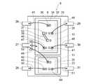
図2は、本実施形態の電源装置に設けられた半導体パッケージの模式的平面配置図である。
照明装置1は、直流電圧源2の出力電圧を所望の電圧に変換する電源装置3と、電源装置3の負荷回路となり電源装置3から電力を供給されて点灯する照明負荷4と、を備えている。照明負荷4は、例えばLEDなどの照明光源を有する。直流電圧源2は、例えば交流電源5と整流器6とを有する。図1においては、直流電圧源2として、交流電源5として例えば商用交流電源の交流電圧を、整流器6として例えばブリッジ形整流回路により整流し、直流電圧を出力するものを示した。FIG. 2 is a schematic plan view of a semiconductor package provided in the power supply device of this embodiment.
The lighting device 1 includes a
電源装置3は、入力フィルタコンデンサ7と、半導体パッケージ8と、ダイオード12、13、14と、定電圧ダイオード15と、抵抗16と、コンデンサ17と、インダクタ18、19と、出力フィルタコンデンサ20と、を備えている。半導体パッケージ8は、第1のスイッチング素子9と、電流制御素子10と、第2のスイッチング素子11と、を有する。これらは、化合物半導体よりなるノーマリーオン型トランジスタであり、例えば、窒化ガリウム(GaN)などの窒化物半導体により形成された高電子移動度トランジスタ(High Electron Mobility Transistor:HEMT)である。ダイオード12は、例えば、シリコンショットキーバリアダイオードである。インダクタ18とインダクタ19とは、磁気結合している。 The
なお、本願明細書において「窒化物半導体」とは、BxInyAlzGa1−x−y−zN(0≦x≦1,0≦y≦1,0≦z≦1,x+y+z≦1)なる化学式において組成比x、y及びzをそれぞれの範囲内で変化させた全ての組成の半導体を含むものとする。またさらに、上記化学式において、N(窒素)以外のV族元素もさらに含むもの、導電型などの各種の物性を制御するために添加される各種の元素をさらに含むもの、及び、意図せずに含まれる各種の元素をさらに含むものも、「窒化物半導体」に含まれるものとする。 In the present specification, the term “nitride semiconductor” refers to a composition ratio x in a chemical formula of BxInyAlzGa1-xyZN (0 ≦ x ≦ 1, 0 ≦ y ≦ 1, 0 ≦ z ≦ 1, x + y + z ≦ 1). , Y and z are included in the respective ranges, and semiconductors having all compositions are included. Furthermore, in the above chemical formula, those further containing a group V element other than N (nitrogen), those further containing various elements added for controlling various physical properties such as conductivity type, and unintentionally Those further including various elements included are also included in the “nitride semiconductor”.
直流電圧源2の出力は、電源装置3の高電位入力端子21と低電位入力端子22との間に入力される。入力フィルタコンデンサ7は、電源装置3の高電位入力端子21と低電位入力端子22との間に接続されている。電源装置3の高電位入力端子21は、第1のスイッチング素子9のドレインに接続され、第1のスイッチング素子9のソースは、第2の電流制御素子10のドレインに接続されている。電流制御素子10のソースは、第2のスイッチング素子11のドレインに接続され、第2のスイッチング素子11のソースは、ダイオード12のカソードに接続されている。 The output of the
ダイオード12のアノードは、電源装置3の低電位入力端子22に接続されている。第2のスイッチング素子11のドレインは、第1のインダクタ18の一端に接続されている。第1のインダクタ18の他端は、出力フィルタコンデンサ20の一端に接続されている。出力フィルタコンデンサ20の他端は、電源装置3の低電位入力端子に接続されている。第2のインダクタ19の一端は、第2のスイッチング素子11のドレインに接続され、他端はコンデンサ17を介して第1のスイッチング素子9のゲートに接続される。第2のインダクタ19は、第1のインダクタ18の電流が増加しているとき第1のスイッチング素子9をオンさせる電圧が誘起され、第1のインダクタ18の電流が減少しているとき、第1のスイッチング素子9をオフさせる電圧が誘起される結線とされている。 The anode of the
ダイオード14のアノードは、第1のスイッチング素子9のゲートに接続され、ダイオード14のカソードは、電流制御素子10のソースに接続されている。ダイオード13のアノードは、電流制御素子10のゲートに接続され、ダイオード13のカソードは、電流制御素子10のソースに接続されている。第2のスイッチング素子11のゲートは、ダイオード12のアノードに接続されている。定電圧ダイオード15のカソードは、第2のスイッチング素子11のドレインに接続され、定電圧ダイオード15のアノードは、抵抗16の一端に接続されている。抵抗16の他端は、電源装置3の低電位入力端子22に接続されている。電流制御素子10のゲートが定電圧ダイオード15のアノードに接続されている。電源装置3の出力は、出力フィルタコンデンサ20の両端から高電位出力端子23、低電位出力端子24に取り出され、照明負荷4に供給される。 The anode of the
図2に示したように、半導体チップ35と、半導体チップ35は、半導体パッケージ8内に実装されている。なお、図2は、半導体パッケージ8の内部構造を模式的に表した平面図であり、実際には、半導体チップ34や半導体チップ35などは、封止樹脂25によりモールドされている。半導体チップ34は、リードフレームのランド(第1の実装基板)32上に実装され、半導体チップ35は、リードフレームのランド(第2の実装基板)33上に実装されている。ランド32、33は、導電性である。これらは、封止樹脂25で覆われてパッケージングされている。 As shown in FIG. 2, the
半導体チップ34は、第1のスイッチング素子9、電流制御素子10を含んでいる。半導体チップ35には、第2のスイッチング素子11を含んでいる。半導体チップ34、35にはボンディングパッドが形成されている。ボンディングパッド36、39、42は、それぞれ第1のスイッチング素子9、電流制御素子10および第2のスイッチング素子11の主端子としてのドレイン電極に対応している。また、ボンディングパッド37、40、43は、それぞれ第1のスイッチング素子9、電流制御素子10および第2のスイッチング素子11の主端子としてのソース電極に対応している。さらに、ボンディングパッド38、41、44は、それぞれ第1のスイッチング素子9、電流制御素子10および第2のスイッチング素子11の制御端子としてのゲート電極に対応している。ボンディングパッド37、39を除いて、これらのボンディングパッドは、それぞれボンディングワイヤー45〜51により近傍のリードフレームに接続されている。 The
これらのリードフレームは、端子26〜31として、外部に引き出されている。スイッチング素子9のドレインは、端子26に接続され、スイッチング素子9のゲートは、端子29に接続されている。電流制御素子10のソースは、端子27に接続され、電流制御素子10のゲートは、端子30に接続されている。スイッチング素子11のドレインは、端子27に接続され、スイッチング素子11のソースは、端子28に接続されている。スイッチング素子11のゲートは、端子31に接続されている。 These lead frames are pulled out as
スイッチング素子9のソースは、パッド間に形成された金属配線53により、電流制御素子10のドレインに接続されている。 The source of the
電流制御素子10のソースは、ボンディングワイヤー47、リードフレーム、ボンディングワイヤー52を介してリードフレームのランド32に電気的に接続されている。 The source of the
次に、電源装置3の動作について説明する。
まず、第2のスイッチング素子11とダイオード12の動作を説明する。これらは整流手段として動作する。ダイオード12のアノード側に正の電圧が印加された場合、ダイオード12は、導通する。ノーマリーオン型の素子である第2のスイッチング素子11も、オンする。順方向に電圧が印加された状態であり、整流手段は、オン状態となる。ダイオード12のアノード側に負の電圧が印加された場合、ダイオード12は、非導通となる。第2のスイッチング素子11のゲート・ソース間Vgs11が負の値となるため、第2のスイッチング素子11も、オフとなる。逆方向に電圧が印加された状態であり、整流手段は、オフ状態となる。Next, the operation of the
First, the operation of the
逆方向に電圧が印加された場合に、ダイオード12にかかる逆電圧は、第2のスイッチング素子11のVgs11である。この電圧は数V程度なため、ダイオード12としては、低耐圧のシリコンショットキーバリアダイオードなどを用いることができる。一般に、低耐圧のシリコンショットキーバリアダイオードは、順電圧が低い。第2のスイッチング素子11のオン時の順電圧も低いため、整流手段全体としてみた順電圧は、GaNダイオード単体より低くすることができる。 When a voltage is applied in the reverse direction, the reverse voltage applied to the
続いて、電流制御素子10の動作を説明する。
定電圧ダイオード15、抵抗16の作用により、電流制御素子10のゲート・ソース間電圧Vgs10は、負の電圧となっている。電流制御素子10は、このVgs10に対応した閾値電流を持つ。電流制御素子10のドレイン電流がこの閾値より小さいとき、電流制御素子10は、低いオン抵抗を示す。ドレイン電流が閾値を超えると、電流制御素子10のオン抵抗が急増し、電流制御素子10は定電流特性を示すようになる。Subsequently, the operation of the
Due to the action of the
このような、第2のスイッチング素子11とダイオード12からなる整流手段、および電流制御素子10の特性を参照しつつ、電源装置3の動作について、以下に説明する。 The operation of the
(1)直流電源2の出力電圧が高電位入力端子21と低電位入力端子22との間に印加されるとき、第1のスイッチング素子9および電流制御素子10は、ノーマリオン型の素子であるため、オン状態にある。すると、高電位入力端子21、第1のスイッチング素子9、電流制御素子10、インダクタ18、出力フィルタコンデンサ20、低電位入力端子22の経路で電流が流れ、出力フィルタコンデンサ20が充電される。インダクタ18には、電磁エネルギーが蓄積される。 (1) When the output voltage of the
(2)第1のスイッチング素子9および電流制御素子10がオンしているため、第2のスイッチング素子11とダイオード12からなる整流手段の両端には、電源装置3の入力電圧が印加される。逆方向に電圧が印加されるため、整流手段は、非導通の状態となる。 (2) Since the
(3)インダクタ18を流れる電流は、時間の経過とともに増加していく。インダクタ19はインダクタ18と磁気結合しているため、インダクタ19には、結合コンデンサとして働くコンデンサ17側を高電位とする極性の起電力が誘起される。第1のスイッチング素子9のゲートには、コンデンサ17を介してソースに対して正の電位が供給され、第1のスイッチング素子9は、オンの状態を維持する。 (3) The current flowing through the
(4)インダクタ18を流れる電流が電流制御素子10の閾値を超えると、電流制御素子10のドレイン・ソース間の電圧は、オン抵抗の急増により、急激に上昇する。第1のスイッチング素子9のゲート・ソース間の電圧が負の大きな値となり、第1のスイッチング素子9は、オフとなる。 (4) When the current flowing through the
(5)インダクタ18には、逆起電力が発生する。順方向に電圧が印加されるため、第2のスイッチング素子11とダイオード12からなる整流手段は、オン状態となる。電流は、整流手段、インダクタ18、出力フィルタコンデンサ20の経路で、流れ続ける。電磁エネルギーを放出するため、インダクタ18の電流は、減少していく。インダクタ19に誘起された負の電圧は、維持され、第1のスイッチング素子9は、オフの状態を継続する。 (5) Back electromotive force is generated in the
(6)インダクタ18に蓄積されていた電磁エネルギーがゼロになると、インダクタ18を流れる電流は、ゼロになる。起電力の方向が再び反転し、インダクタ19には、コンデンサ17側を高電位とするような起電力が誘起される。第1のスイッチング素子9のゲートにソースよりも高い電圧が供給され、第1のスイッチング素子9は、オンする。上記(1)の状態に戻る。 (6) When the electromagnetic energy accumulated in the
以後、(1)〜(6)を繰り返す。入力電圧は、変換されて、照明負荷4に供給される。第1の実施形態では電源装置3は、降圧コンバータとして動作する。ダイオード13、14は、それぞれ、第1のスイッチング素子9、電流制御素子10のゲートの電位を制限する。 Thereafter, (1) to (6) are repeated. The input voltage is converted and supplied to the
ところで、GaN系半導体により形成されたHEMTでは、ドレイン電流がドレイン・ソース間電圧の影響を受ける、電流コラプスという現象がある。高電圧が印加された直後のGaN HEMTのオン抵抗が高くなるという現象である。対策として、GaN HEMTのソース端子または、ゲート端子をリードフレームのランドに電気的に接続する方法がある。 By the way, in the HEMT formed of a GaN-based semiconductor, there is a phenomenon called current collapse in which the drain current is affected by the drain-source voltage. This is a phenomenon in which the on-resistance of the GaN HEMT immediately after a high voltage is applied increases. As a countermeasure, there is a method of electrically connecting the source terminal or gate terminal of the GaN HEMT to the land of the lead frame.
対策の効果を表1を用いて説明する。
表1は、GaN HEMTの電圧印加前後のオン抵抗の変化を例示する表である。すなわち、表1は、GaN HEMTのドレイン・ソース間に500Vの電圧を印加する前後のオン抵抗の変化を、電圧印加前を基準として表したものである。
ソースまたはゲートをリードフレームのランドに接続した場合、接続しない場合に比べて、オン抵抗の増加が少ないことが分かる。前述したように、図2に表した半導体パッケージでは、電流制御素子10のソースがリードフレームのランド33に接続されている。こうすることにより、スイッチング素子9と電流制御素子10について電流コラプスの影響を小さくすることができる。The effect of the countermeasure will be described with reference to Table 1.
Table 1 is a table exemplifying a change in on-resistance before and after voltage application of the GaN HEMT. That is, Table 1 shows changes in on-resistance before and after applying a voltage of 500 V between the drain and source of the GaN HEMT, with reference to before voltage application.
It can be seen that when the source or gate is connected to the land of the lead frame, the increase in on-resistance is smaller than when the source or gate is not connected. As described above, in the semiconductor package shown in FIG. 2, the source of the
他の効果について、図3を用いて説明する。
図3は、GaN HEMTのリーク電流特性を示す特性図である。
図3の横軸はGaN HEMTとダイオードによる整流手段に逆電圧を印加し、GaN HEMTをオフ状態とした場合の、GaN HEMTのドレイン・ゲート間電圧Vdgを表す。図3の縦軸は、第1軸がソース・ゲート間電圧Vsgを表し、第2軸がリーク電流IR表す。Other effects will be described with reference to FIG.
FIG. 3 is a characteristic diagram showing leakage current characteristics of the GaN HEMT.
The horizontal axis of FIG. 3 represents the drain-gate voltage Vdg of the GaN HEMT when a reverse voltage is applied to the rectifying means using the GaN HEMT and the diode to turn off the GaN HEMT. In the vertical axis of FIG. 3, the first axis represents the source-gate voltage Vsg, and the second axis represents the leakage current IR.
ゲートをリードフレームのランドに接続した場合は、Vdgの増加に伴ってIRも増加することが分かる。IRが増加すると、電源装置の変換効率が低下することとなる。IRの増加は、Vsgの増加も引き起こし、さらなる変換効率低下の原因となる。順方向電圧を印加し、GaN HEMTをオンさせるためには、Vsgを放電する必要があり、この放電電力が損失となるためである。 It can be seen that when the gate is connected to the land of the lead frame, the IR increases as Vdg increases. If IR increases, the conversion efficiency of a power supply device will fall. An increase in IR also causes an increase in Vsg, causing further reduction in conversion efficiency. This is because in order to apply a forward voltage and turn on the GaN HEMT, it is necessary to discharge Vsg, and this discharge power is lost.
一方、ソースをリードフレームのランドに接続した場合や、どの端子も接続しない場合、IRとVsgは、ほとんど増加しない。 On the other hand, when the source is connected to the land of the lead frame or when no terminal is connected, IR and Vsg hardly increase.
これらの結果から、GaN HEMTのソースをリードフレームのランドに接続することによって、電流コラプスとリーク電流の両者に対処可能なことが分かる。 From these results, it can be seen that both current collapse and leakage current can be dealt with by connecting the source of the GaN HEMT to the land of the lead frame.
第1の実施形態の効果について説明する。第1のスイッチング素子9、電流制御素子10、第2のスイッチング素子11を一つの半導体パッケージ8に実装することにより、小型化できるという効果が得られる。電流制御素子のソースをリードフレームのランドに接続することにより、電流コラプスの影響を小さくし、オン抵抗の増加が抑えられる。同時に、リーク電流の増加も抑えることができる。これらにより、変換効率の低下を抑えるという効果も得られる。 The effect of the first embodiment will be described. By mounting the
なお、本実施形態においては、半導体パッケージ8において端子27を端子26および28と同一の側部に設けたが、端子27を端子29〜31と同じ半導体パッケージ8の側部に設けてもよい。端子27を端子29〜31と同じ側部に設けることで、直流電圧または低周波の脈流が印加される部分と高周波が印加される部分を分けることができ、半導体パッケージ8において、沿面距離を確保できるとともに半導体パッケージ8への静電気対策が可能になる。 In the present embodiment, the terminal 27 is provided on the same side as the
(第2実施形態)
第2の実施形態について説明する。
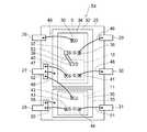
図4は、第2の実施形態に係る電源装置に設けられた半導体パッケージの模式平面配置図である。
第2の実施形態に係る電源装置の他の部分は、第1の実施形態と同様とすることができる。(Second Embodiment)
A second embodiment will be described.
FIG. 4 is a schematic plan layout view of a semiconductor package provided in the power supply device according to the second embodiment.
Other parts of the power supply device according to the second embodiment can be the same as those of the first embodiment.
本実施形態の電源装置の半導体パッケージ54は、第1実施形態の半導体パッケージ8に対して、ボンディングワイヤー55による接続を追加したものである。第2のスイッチング素子11のソースは、ボンディングワイヤー50、リードフレーム、ボンディングワイヤー55を介して、リードフレームのランド33に電気的に接続されている。図4から明らかなように、ランド32とランド33とは、分離されている。 The
第2のスイッチング素子11のソースが、リードフレームのランド33に接続されているため、第2のスイッチング素子11についても、電流コラプスとリーク電流の影響を小さくすることができる。 Since the source of the
ところで、第1のスイッチング素子9、電流制御素子10、第2のスイッチング素子11が、単一のランド上に配置され、電流制御素子10のソースではなく、第2のスイッチング素子11のソースが当該ランドに接続されるという構造も考えられる。しかし、この構造の場合、次のような問題が生じる。 By the way, the
第2のスイッチング素子11のソースを単一のランドに接続したため、第2のスイッチング素子11のドレイン・ソース間は、大きな容量が接続された状態となる。この様子を図5に示す。 Since the source of the
図5は、半導体パッケージの模式回路図である。
第1のスイッチング素子9、電流制御素子10、第2のスイッチング素子11は、ランド32上に配置されている。第2のスイッチング素子11のソースは、ボンディングワイヤー50、55を介してランド32に接続されている。Cdsは、並列接続された第2のスイッチング素子11のドレイン・ソース間容量とドレイン・ランド間容量とを足し合わせたものである。Cdは、ダイオード12の容量である。FIG. 5 is a schematic circuit diagram of the semiconductor package.
The
Cdsは、大きな面積のランド32が第2のスイッチング素子11のソースに接続されたため、Cdに対して大きな値となる。第1のスイッチング素子9と電流制御素子10がオン状態の時、第2のスイッチング素子11とダイオード12には、電源装置3の入力電圧をCdsとCdで分圧した電圧が印加される。Cdに対しCdsが大きいため、ダイオード12には、比較的大きな電圧が印加される。第2のスイッチング素子11のゲート・ソース間の耐圧を超えてしまい、第2のスイッチング素子11は、破壊されるおそれがある。 Cds has a large value with respect to Cd because the
次に、ランドを3つに分ける場合について検討する。
第1のスイッチング素子9、電流制御素子10、第2のスイッチング素子11を単一の半導体チップとする。各半導体チップをそれぞれランドに配置し、かつソースをそれぞれのランドに接続する。この構造の場合も、問題が生じる。Next, consider the case where the land is divided into three.
The
高電圧が印加されるため、第1のスイッチング素子9では、この構造は、電流コラプス、リーク電流対策として、有効である。一方、第1のスイッチング素子9のドレイン・ソース間には、図5におけるスイッチング素子11と同様に、大きな容量が接続された状態となる。このため、第1のスイッチング素子9のスイッチング動作が遅くなってしまうという問題が生じる。 Since a high voltage is applied, in the
一方、電流制御素子10では、オフ状態の時の印加電圧が低いため、電流コラプスがあまり問題とはならない。電流制御素子10のソースをランドに接続する必要性は、ほとんど無い。 On the other hand, in the
以上の検討を踏まえ、図4の実施形態に示したように、第1のスイッチング素子9と電流制御素子10は、ランド32に配置され、第2のスイッチング素子11は、これと異なるランド33に配置される。電流制御素子10のソースをランド32に接続し、第2のスイッチング素子11のソースをランド33に接続する方式が望ましい形態であると考えられる。 Based on the above consideration, as shown in the embodiment of FIG. 4, the
第2の実施形態の効果について、説明する。
第1の実施形態と同様、第1のスイッチング素子9、電流制御素子10、第2のスイッチング素子11を一つの半導体パッケージ54に実装することにより小型化できるという効果が得られる。第1のスイッチング素子9、電流制御素子10だけでなく、第2のスイッチング素子11の電流コラプスとリーク電流の影響も抑えることができ、変換効率の低下を抑えるという効果も得られる。The effect of the second embodiment will be described.
Similar to the first embodiment, by mounting the
なお、本実施形態も第1の実施形態と同様に端子27を端子29〜31と同じ半導体パッケージ54の側部に設けてもよい。端子27を端子29〜31と同じ側部に設けることで、直流電圧または低周波の脈流が印加される部分と高周波が印加される部分を分けることができ、半導体パッケージ54において、沿面距離を確保できるとともに半導体パッケージ54への静電気対策が可能になる。 In the present embodiment, the terminal 27 may be provided on the same side of the
(第3実施形態)
次に、第3の実施形態について説明する。
図6は、第3の実施形態に係る電源装置を含む照明装置の回路図である。(Third embodiment)
Next, a third embodiment will be described.
FIG. 6 is a circuit diagram of a lighting device including the power supply device according to the third embodiment.
図7は、本実施形態の電源装置に設けられた半導体パッケージの模式平面配置図である。
図6に表したように、照明装置56は、直流電圧源2と、電源装置57と、照明負荷4と、を備えている。FIG. 7 is a schematic plan view of a semiconductor package provided in the power supply device of this embodiment.
As illustrated in FIG. 6, the
電源装置57は、入力フィルタコンデンサ7と、半導体パッケージ58と、ダイオード13、14と、定電圧ダイオード15と、抵抗16と、コンデンサ17と、インダクタ18、19と、出力フィルタコンデンサ20と、を有する。 The
図7に表したように、本実施形態における半導体パッケージ58は、第1のスイッチング素子9と、電流制御素子10と、第2のスイッチング素子11と、ダイオード12と、を有している。ダイオード12は、第2のスイッチング素子11と同じGaN半導体である。 As shown in FIG. 7, the
ボンディングパッド59は、アノード電極に対応し、ボンディングパッド60は、カソード電極に対応している。ダイオード12のアノードは、ボンディングワイヤー61を介して端子31に接続されている。スイッチング素子11のソースは、パッド間に形成された金属配線62により、ダイオード12のカソードに接続されている。 The
本実施形態の電源装置は、第1の実施の形態の電源装置3において、半導体パッケージ8内にダイオード12が含まれ、半導体パッケージ58とされたものである。これ以外は、第1の実施の形態の電源装置3と同様とすることができる。電源装置57の動作も、電源装置3と同じである。 The power supply device according to the present embodiment is the same as the
第3の実施形態の効果について説明する。本実施形態によれば、第1の実施形態と同様に、第1のスイッチング素子9と電流制御素子10の電流コラプスとリーク電流の影響を抑えることができ、変換効率の低下を抑えるという効果が得られる。第1のスイッチング素子9、電流制御素子10、第2のスイッチング素子11、ダイオード12がひとつの半導体パッケージ58内に実装されているため、第1の実施形態以上に小型化できるという効果も得られる。 The effect of the third embodiment will be described. According to the present embodiment, as in the first embodiment, the effects of current collapse and leakage current of the
なお、本実施形態も第1および2の実施形態と同様に端子27を端子29〜31と同じ半導体パッケージ58の側部に設けてもよい。端子27を端子29〜31と同じ側部に設けることで、直流電圧または低周波の脈流が印加される部分と高周波が印加される部分を分けることができ、半導体パッケージ58において、沿面距離を確保できるとともに半導体パッケージ58への静電気対策が可能になる。 In this embodiment as well, the
以上、具体例を参照しつつ実施形態について説明したが、それらに限定されるものではなく、種々の変形が可能である。 As described above, the embodiments have been described with reference to specific examples. However, the embodiments are not limited thereto, and various modifications are possible.
例えば、第1のスイッチング素子9、電流制御素子10および第2のスイッチング素子11はGaN系HEMTには限定されない。例えば、半導体基板に炭化珪素(SiC)や窒化ガリウム(GaN)やダイヤモンドのようなワイドバンドギャップを有する半導体(ワイドバンドギャップ半導体)を用いて形成した半導体素子でもよい。ここで、ワイドバンドギャップ半導体とは、バンドギャップが約1.4eVのヒ化ガリウム(GaAs)よりもバンドギャップの広い半導体をいう。例えば、バンドギャップが1.5eV以上の半導体、リン化ガリウム(GaP、バンドギャップ約2.3eV)、窒化ガリウム(GaN、バンドギャップ約3.4eV)、ダイアモンド(C、バンドギャップ約5.27eV)、窒化アルミニウム(AlN、バンドギャップ約5.9eV)、炭化ケイ素(SiC)などが含まれる。 For example, the
なお、照明負荷4はLEDに限らず、例えば、有機EL(Electro-Luminescence)やOLED(Organic light-emitting diode)などでもよい。 The
以上、具体例を参照しつつ実施形態について説明した。しかし、実施形態はこれらの具体例に限定されるものではない。すなわち、これら具体例に、当業者が適宜設計変更を加えたものも、実施形態の特徴を備えている限り、実施形態の範囲に包含される。前述した各具体例が備える各要素およびその配置、材料、条件、形状、サイズなどは、例示したものに限定されるわけではなく適宜変更することができる。 The embodiment has been described above with reference to specific examples. However, the embodiments are not limited to these specific examples. In other words, those specific examples that have been appropriately modified by those skilled in the art are also included in the scope of the embodiments as long as they include the features of the embodiments. Each element included in each of the specific examples described above and their arrangement, material, condition, shape, size, and the like are not limited to those illustrated, and can be appropriately changed.
また、前述した各実施形態が備える各要素は、技術的に可能な限りにおいて複合させることができ、これらを組み合わせたものも実施形態の特徴を含む限り実施形態の範囲に包含される。その他、実施形態の思想の範疇において、当業者であれば、各種の変更例および修正例に想到し得るものであり、それら変更例および修正例についても実施形態の範囲に属するものと了解される。 In addition, each element included in each of the above-described embodiments can be combined as long as technically possible, and combinations thereof are also included in the scope of the embodiment as long as they include the features of the embodiment. In addition, in the category of the idea of the embodiment, those skilled in the art can conceive various changes and modifications, and it is understood that these changes and modifications also belong to the scope of the embodiment. .
本発明のいくつかの実施形態を説明したが、これらの実施形態は、例として提示したものであり、発明の範囲を限定することは意図していない。これら新規な実施形態は、その他の様々な形態で実施されることが可能であり、発明の要旨を逸脱しない範囲で、種々の省略、置き換え、変更を行うことができる。これら実施形態やその変形は、発明の範囲や要旨に含まれるとともに、特許請求の範囲に記載された発明とその均等の範囲に含まれる。 Although several embodiments of the present invention have been described, these embodiments are presented by way of example and are not intended to limit the scope of the invention. These novel embodiments can be implemented in various other forms, and various omissions, replacements, and changes can be made without departing from the scope of the invention. These embodiments and modifications thereof are included in the scope and gist of the invention, and are included in the invention described in the claims and the equivalents thereof.
1…照明装置、2…直流電圧源、3…電源装置、4…照明負荷、5…交流電源、6…整流器、7…入力フィルタコンデンサ、8…半導体パッケージ、9…スイッチング素子、10…電流制御素子、11…スイッチング素子、12〜14…ダイオード、15…定電圧ダイオード、16…抵抗、17…コンデンサ、18、19…インダクタ、20…出力フィルタコンデンサ、21…高電位入力端子、22…低電位入力端子、23…高電位出力端子、24…低電位出力端子、25…封止樹脂、26〜31…端子、32、33…ランド、34、35…半導体チップ、36〜44…ボンディングパッド、45〜52…ボンディングワイヤー、53…金属配線、54…半導体パッケージ、55…ボンディングワイヤー、56…照明装置、57…電源装置、58…半導体パッケージ、59…ボンディングパッド、59…半導体パッケージ、60…ボンディングパッド、61…ボンディングワイヤー、62…金属配線 DESCRIPTION OF SYMBOLS 1 ... Illuminating device, 2 ... DC voltage source, 3 ... Power supply device, 4 ... Illumination load, 5 ... AC power supply, 6 ... Rectifier, 7 ... Input filter capacitor, 8 ... Semiconductor package, 9 ... Switching element, 10 ...
Claims (5)
Translated fromJapanese前記第1の実装基板の上に実装された第1のスイッチング素子と、
前記第1の実装基板の上に実装され、前記第1の実装基板に接続された主端子を有し、前記第1のスイッチング素子と直列に接続され、前記第1のスイッチング素子の電流を制限する電流制御素子と、
前記電流制御素子に直列に接続され、前記第1のスイッチング素子がオフのとき電流が流れる第2のスイッチング素子と、
を備え、
前記電流制御素子はHEMTであり、前記主端子は前記HEMTのソース端子である電源装置。A conductive first mounting substrate;
A first switching element mounted on the first mounting substrate;
A main terminal mounted on the first mounting board and connected to the first mounting board, connected in series with the first switching element, and limiting a current of the first switching element Current control element to
A second switching element connected in series to the current control element and through which a current flows when the first switching element is off;
Equipped witha,
The power supply device,wherein the current control element is a HEMT and the main terminal is a source terminal of the HEMT .
前記第2のスイッチング素子の主端子は、前記第2の実装基板と接続され、
前記第1の実装基板と、前記第2の実装基板とは、分離されている請求項1に記載の電源装置。A second mounting board on which the second switching element is mounted;
The main terminal of the second switching element is connected to the second mounting substrate,
The power supply device according to claim 1, wherein the first mounting board and the second mounting board are separated.
前記電源装置の負荷回路となる照明負荷と、
を備えた照明装置。The power supply device according to any one of claims 1 to 4,
A lighting load serving as a load circuit of the power supply device;
A lighting device comprising:
Priority Applications (4)
| Application Number | Priority Date | Filing Date | Title |
|---|---|---|---|
| JP2013198451AJP6156643B2 (en) | 2013-09-25 | 2013-09-25 | Power supply device and lighting device |
| EP20140159159EP2863710A2 (en) | 2013-09-25 | 2014-03-12 | Power supply device and luminaire |
| US14/211,214US20150084530A1 (en) | 2013-09-25 | 2014-03-14 | Power Supply Device and Luminaire |
| CN201410095297.4ACN104470048B (en) | 2013-09-25 | 2014-03-14 | Supply unit and lighting device |
Applications Claiming Priority (1)
| Application Number | Priority Date | Filing Date | Title |
|---|---|---|---|
| JP2013198451AJP6156643B2 (en) | 2013-09-25 | 2013-09-25 | Power supply device and lighting device |
Related Child Applications (1)
| Application Number | Title | Priority Date | Filing Date |
|---|---|---|---|
| JP2017113136ADivisionJP6388181B2 (en) | 2017-06-08 | 2017-06-08 | Semiconductor package and power supply device |
Publications (2)
| Publication Number | Publication Date |
|---|---|
| JP2015065044A JP2015065044A (en) | 2015-04-09 |
| JP6156643B2true JP6156643B2 (en) | 2017-07-05 |
Family
ID=50241235
Family Applications (1)
| Application Number | Title | Priority Date | Filing Date |
|---|---|---|---|
| JP2013198451AActiveJP6156643B2 (en) | 2013-09-25 | 2013-09-25 | Power supply device and lighting device |
Country Status (4)
| Country | Link |
|---|---|
| US (1) | US20150084530A1 (en) |
| EP (1) | EP2863710A2 (en) |
| JP (1) | JP6156643B2 (en) |
| CN (1) | CN104470048B (en) |
Families Citing this family (8)
| Publication number | Priority date | Publication date | Assignee | Title |
|---|---|---|---|---|
| US8488342B2 (en) | 2008-10-21 | 2013-07-16 | On-Bright Electronics (Shanghai) Co., Ltd. | Systems and methods for constant voltage mode and constant current mode in flyback power converters with primary-side sensing and regulation |
| CN102769383B (en) | 2011-05-05 | 2015-02-04 | 广州昂宝电子有限公司 | System and method for constant-current control via primary side sensing and regulating |
| CN105246194B (en) | 2011-11-15 | 2018-07-03 | 昂宝电子(上海)有限公司 | For the LED illumination System and method of the current constant control in various operation modes |
| CN103368400B (en) | 2012-03-31 | 2015-02-18 | 昂宝电子(上海)有限公司 | System and method for constant voltage control and constant current control |
| CN102790531B (en) | 2012-07-24 | 2015-05-27 | 昂宝电子(上海)有限公司 | System for electric current control of power supply alternation system |
| CN103956900B (en)* | 2014-04-23 | 2017-08-11 | 广州昂宝电子有限公司 | Systems and methods for output current regulation in power conversion systems |
| US9991776B2 (en)* | 2015-12-16 | 2018-06-05 | Semiconductor Components Industries, Llc | Switched mode power supply converter |
| JP7178184B2 (en)* | 2018-06-07 | 2022-11-25 | ローム株式会社 | semiconductor equipment |
Family Cites Families (5)
| Publication number | Priority date | Publication date | Assignee | Title |
|---|---|---|---|---|
| JP5358882B2 (en)* | 2007-02-09 | 2013-12-04 | サンケン電気株式会社 | Composite semiconductor device including rectifying element |
| JP5297104B2 (en)* | 2008-07-01 | 2013-09-25 | ルネサスエレクトロニクス株式会社 | Semiconductor device |
| JP5751483B2 (en)* | 2010-06-28 | 2015-07-22 | 東芝ライテック株式会社 | Switching power supply device, switching power supply circuit, and electrical equipment |
| JP2013013231A (en)* | 2011-06-29 | 2013-01-17 | Toshiba Lighting & Technology Corp | Switching power supply and illumination apparatus |
| JP5780428B2 (en)* | 2011-09-20 | 2015-09-16 | 東芝ライテック株式会社 | Switching power supply and lighting device |
- 2013
- 2013-09-25JPJP2013198451Apatent/JP6156643B2/enactiveActive
- 2014
- 2014-03-12EPEP20140159159patent/EP2863710A2/ennot_activeWithdrawn
- 2014-03-14CNCN201410095297.4Apatent/CN104470048B/enactiveActive
- 2014-03-14USUS14/211,214patent/US20150084530A1/ennot_activeAbandoned
Also Published As
| Publication number | Publication date |
|---|---|
| CN104470048B (en) | 2018-09-18 |
| JP2015065044A (en) | 2015-04-09 |
| CN104470048A (en) | 2015-03-25 |
| EP2863710A2 (en) | 2015-04-22 |
| US20150084530A1 (en) | 2015-03-26 |
Similar Documents
| Publication | Publication Date | Title |
|---|---|---|
| JP6156643B2 (en) | Power supply device and lighting device | |
| US8497573B2 (en) | High power semiconductor package with conductive clip on multiple transistors | |
| JP2013013231A (en) | Switching power supply and illumination apparatus | |
| TWI663893B (en) | Led driver and illumination system related to the same | |
| JP6388181B2 (en) | Semiconductor package and power supply device | |
| JP5831807B2 (en) | Lighting power supply and lighting device | |
| JP5660351B2 (en) | Switching power supply and lighting device | |
| US8767413B2 (en) | Integrated switching power supply device and electric apparatus | |
| TWI678946B (en) | Led driver and illumination system related to the same | |
| JP7242487B2 (en) | semiconductor equipment | |
| US20150084528A1 (en) | Power Supply Device and Luminaire | |
| CN104467468A (en) | Rectifying circuit, electronic circuit, and electronic apparatus | |
| TW201715915A (en) | LED driver and illumination system related to the same | |
| CN105188225A (en) | LED (Light Emitting Diode) driver and LED lamp | |
| JP2015029040A (en) | Semiconductor module, LED driving device, and LED lighting device | |
| JP2014183639A (en) | Power-supply device and lighting device | |
| JP2015065776A (en) | Power supply device and lighting device | |
| TWI729540B (en) | Led driver and illumination system related to the same | |
| CN104470051A (en) | Power supply unit and lighting unit | |
| CN104467399A (en) | Switching power device and lighting device |
Legal Events
| Date | Code | Title | Description |
|---|---|---|---|
| A621 | Written request for application examination | Free format text:JAPANESE INTERMEDIATE CODE: A621 Effective date:20160322 | |
| A131 | Notification of reasons for refusal | Free format text:JAPANESE INTERMEDIATE CODE: A131 Effective date:20161206 | |
| A521 | Written amendment | Free format text:JAPANESE INTERMEDIATE CODE: A523 Effective date:20170206 | |
| TRDD | Decision of grant or rejection written | ||
| A01 | Written decision to grant a patent or to grant a registration (utility model) | Free format text:JAPANESE INTERMEDIATE CODE: A01 Effective date:20170510 | |
| A61 | First payment of annual fees (during grant procedure) | Free format text:JAPANESE INTERMEDIATE CODE: A61 Effective date:20170523 | |
| R151 | Written notification of patent or utility model registration | Ref document number:6156643 Country of ref document:JP Free format text:JAPANESE INTERMEDIATE CODE: R151 |