JP6143485B2 - Electronic device and antenna device - Google Patents
Electronic device and antenna deviceDownload PDFInfo
- Publication number
- JP6143485B2 JP6143485B2JP2013021617AJP2013021617AJP6143485B2JP 6143485 B2JP6143485 B2JP 6143485B2JP 2013021617 AJP2013021617 AJP 2013021617AJP 2013021617 AJP2013021617 AJP 2013021617AJP 6143485 B2JP6143485 B2JP 6143485B2
- Authority
- JP
- Japan
- Prior art keywords
- coil
- magnetic sheet
- module
- loop coil
- internal structure
- Prior art date
- Legal status (The legal status is an assumption and is not a legal conclusion. Google has not performed a legal analysis and makes no representation as to the accuracy of the status listed.)
- Active
Links
Images


Classifications
- H—ELECTRICITY
- H01—ELECTRIC ELEMENTS
- H01Q—ANTENNAS, i.e. RADIO AERIALS
- H01Q1/00—Details of, or arrangements associated with, antennas
- H01Q1/12—Supports; Mounting means
- H01Q1/22—Supports; Mounting means by structural association with other equipment or articles
- H01Q1/24—Supports; Mounting means by structural association with other equipment or articles with receiving set
- H01Q1/241—Supports; Mounting means by structural association with other equipment or articles with receiving set used in mobile communications, e.g. GSM
- H01Q1/242—Supports; Mounting means by structural association with other equipment or articles with receiving set used in mobile communications, e.g. GSM specially adapted for hand-held use
- H01Q1/243—Supports; Mounting means by structural association with other equipment or articles with receiving set used in mobile communications, e.g. GSM specially adapted for hand-held use with built-in antennas
- H—ELECTRICITY
- H01—ELECTRIC ELEMENTS
- H01Q—ANTENNAS, i.e. RADIO AERIALS
- H01Q1/00—Details of, or arrangements associated with, antennas
- H01Q1/12—Supports; Mounting means
- H01Q1/22—Supports; Mounting means by structural association with other equipment or articles
- H01Q1/24—Supports; Mounting means by structural association with other equipment or articles with receiving set
- H01Q1/248—Supports; Mounting means by structural association with other equipment or articles with receiving set provided with an AC/DC converting device, e.g. rectennas
- H—ELECTRICITY
- H01—ELECTRIC ELEMENTS
- H01Q—ANTENNAS, i.e. RADIO AERIALS
- H01Q1/00—Details of, or arrangements associated with, antennas
- H01Q1/36—Structural form of radiating elements, e.g. cone, spiral, umbrella; Particular materials used therewith
- H01Q1/38—Structural form of radiating elements, e.g. cone, spiral, umbrella; Particular materials used therewith formed by a conductive layer on an insulating support
- H—ELECTRICITY
- H01—ELECTRIC ELEMENTS
- H01Q—ANTENNAS, i.e. RADIO AERIALS
- H01Q1/00—Details of, or arrangements associated with, antennas
- H01Q1/40—Radiating elements coated with or embedded in protective material
- H—ELECTRICITY
- H01—ELECTRIC ELEMENTS
- H01Q—ANTENNAS, i.e. RADIO AERIALS
- H01Q1/00—Details of, or arrangements associated with, antennas
- H01Q1/52—Means for reducing coupling between antennas; Means for reducing coupling between an antenna and another structure
- H—ELECTRICITY
- H01—ELECTRIC ELEMENTS
- H01Q—ANTENNAS, i.e. RADIO AERIALS
- H01Q7/00—Loop antennas with a substantially uniform current distribution around the loop and having a directional radiation pattern in a plane perpendicular to the plane of the loop
- H—ELECTRICITY
- H01—ELECTRIC ELEMENTS
- H01Q—ANTENNAS, i.e. RADIO AERIALS
- H01Q7/00—Loop antennas with a substantially uniform current distribution around the loop and having a directional radiation pattern in a plane perpendicular to the plane of the loop
- H01Q7/06—Loop antennas with a substantially uniform current distribution around the loop and having a directional radiation pattern in a plane perpendicular to the plane of the loop with core of ferromagnetic material
- H—ELECTRICITY
- H04—ELECTRIC COMMUNICATION TECHNIQUE
- H04B—TRANSMISSION
- H04B5/00—Near-field transmission systems, e.g. inductive or capacitive transmission systems
- H04B5/20—Near-field transmission systems, e.g. inductive or capacitive transmission systems characterised by the transmission technique; characterised by the transmission medium
- H04B5/24—Inductive coupling
- H04B5/26—Inductive coupling using coils
- H04B5/266—One coil at each side, e.g. with primary and secondary coils
- H—ELECTRICITY
- H04—ELECTRIC COMMUNICATION TECHNIQUE
- H04B—TRANSMISSION
- H04B5/00—Near-field transmission systems, e.g. inductive or capacitive transmission systems
- H04B5/40—Near-field transmission systems, e.g. inductive or capacitive transmission systems characterised by components specially adapted for near-field transmission
- H04B5/43—Antennas
- H—ELECTRICITY
- H04—ELECTRIC COMMUNICATION TECHNIQUE
- H04M—TELEPHONIC COMMUNICATION
- H04M1/00—Substation equipment, e.g. for use by subscribers
- H04M1/02—Constructional features of telephone sets
- H04M1/0202—Portable telephone sets, e.g. cordless phones, mobile phones or bar type handsets
- H04M1/026—Details of the structure or mounting of specific components
Landscapes
- Engineering & Computer Science (AREA)
- Computer Networks & Wireless Communication (AREA)
- Signal Processing (AREA)
- Support Of Aerials (AREA)
- Details Of Aerials (AREA)
- Near-Field Transmission Systems (AREA)
- Telephone Set Structure (AREA)
Description
Translated fromJapanese本発明は、ループコイルと磁性シートとを備えたコイルモジュールが内蔵された電子機器及びアンテナ装置に関する。 The present invention relates to an electronic apparatus and an antenna device in which a coil module including a loop coil and a magnetic sheet is incorporated.
近年の無線通信機器においては、電話通信用アンテナ、GPS用アンテナ、無線LAN/BLUETOOTH(登録商標)用アンテナ、さらにはRFID(Radio Frequency Identification)といった複数のRFアンテナが搭載されている。これらに加えて、非接触充電の導入に伴って、電力伝送用のループコイルも搭載されるようになってきた。非接触充電方式で用いられる電力伝送方式には、電磁誘導方式、電波受信方式、磁気共鳴方式等が挙げられる。これらは、いずれも一次側コイルと二次側コイル間の電磁誘導や磁気共鳴を利用したものであり、たとえば非接触充電のQi規格やRFIDのNFC(Near Field Communication)規格では、電磁誘導を利用している。 In recent wireless communication devices, a plurality of RF antennas such as a telephone communication antenna, a GPS antenna, a wireless LAN / BLUETOOTH (registered trademark) antenna, and an RFID (Radio Frequency Identification) are mounted. In addition to these, with the introduction of non-contact charging, loop coils for power transmission have also been installed. Examples of the power transmission method used in the non-contact charging method include an electromagnetic induction method, a radio wave reception method, and a magnetic resonance method. These use electromagnetic induction and magnetic resonance between the primary coil and the secondary coil. For example, the Qi standard for non-contact charging and the NFC (Near Field Communication) standard for RFID use electromagnetic induction. doing.
これらのアンテナは、アンテナ単体で目的の周波数において最大の特性が得られるように設計されていても、実際に電子機器に実装されると、目的の特性を得ることは困難である。これは、アンテナ周辺の磁界成分が周辺に位置する金属等と干渉(結合)し、アンテナコイルのインダクタンスが実質的に減少するために、共振周波数がシフトしてしまうことによる。また、インダクタンスの実質的減少によって、受信感度が低下してしまう。これらの対策として、アンテナコイルとその周辺に存在する金属との間にフェライト等の磁性材料からなる磁気シールド材を介在させることによって、アンテナコイルから発生した磁束を磁気シールド材に集めることによって、金属による干渉を低減させることができる。 Even if these antennas are designed so that the maximum characteristics can be obtained at a target frequency with a single antenna, it is difficult to obtain the target characteristics when actually mounted on an electronic device. This is because the magnetic field component around the antenna interferes (couples) with the surrounding metal and the like, and the inductance of the antenna coil is substantially reduced, so that the resonance frequency is shifted. In addition, the reception sensitivity is lowered due to a substantial decrease in inductance. As a countermeasure for these problems, by interposing a magnetic shield material made of a magnetic material such as ferrite between the antenna coil and the metal existing in the vicinity thereof, the magnetic flux generated from the antenna coil is collected on the magnetic shield material. The interference due to can be reduced.
携帯端末機器等の電子機器の小型化、高機能化による部品点数の増大、消費電力の増加によるバッテリ容量の増加等に伴い、電子機器筐体内において、上述のようなコイルモジュールを搭載するのに割り当てられるスペースは極めて小さくなってきている。そこで、RFID用のアンテナモジュールや非接触充電用の充電モジュールを狭小化されたスペースに搭載するために、モジュールの薄型化の要求が強まっている。 In order to mount the coil module as described above in the electronic device casing as the number of parts is increased due to downsizing and high functionality of electronic devices such as portable terminal devices and the battery capacity is increased due to the increase in power consumption. The allocated space is becoming very small. Therefore, in order to mount an RFID antenna module and a charging module for non-contact charging in a narrowed space, there is an increasing demand for a thinner module.
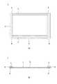
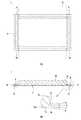
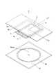
ここで、図17(A)及び図17(B)に示すように、一般的なアンテナモジュール60は、スパイラルコイル状のアンテナコイル61に磁束集束用の磁性シート62を、接着剤を塗布した接着剤層63によって貼付した構成となっている。そして、図18に示すように、シート状のアンテナモジュール60は、電子機器に搭載される際、配置スペースの制約上、多くの場合バッテリ65の金属筐体65aの主面部と重畳する位置に配置される。 Here, as shown in FIGS. 17A and 17B, a
このため、この電子機器は、バッテリ65の厚さに加えてアンテナモジュール60全体の厚さが加わることから、さらなる薄型化が求められていた。一方で、アンテナモジュール60全体の薄型化を図るべく、磁性シート62を薄く形成すると、磁気シールドの効果が減少し、通信特性に影響が出るため、薄型化を図るにも限界があった。 For this reason, since the thickness of the
そこで、本発明は、コイルモジュールの特性を損なうことなく、薄型化を実現し、狭小化されたスペースにも搭載可能なコイルモジュールを用いた電子機器を提供することを目的とする。 Accordingly, an object of the present invention is to provide an electronic apparatus using a coil module that can be thinned and can be mounted in a narrow space without impairing the characteristics of the coil module.
上述した課題を解決するために、本発明に係る電子機器は、面状に巻回されたループコイルと、磁性材料により形成され、上記ループコイルの少なくとも一部と重畳するシート状の磁性シートとを有するコイルモジュールを備え、上記コイルモジュールは、上記ループコイルの一部が筐体の内部構造物と重畳されるとともに、上記磁性シートが、上記ループコイルの上記内部構造物と重畳する面側の上記内部構造物と重畳しない位置に設けられ、上記内部構造物は、一部又は全部が金属体であるものである。In order to solve the above-described problems, an electronic apparatus according to the present invention includes a loop coil wound in a planar shape, a sheet-like magnetic sheet formed of a magnetic material and overlapping at least a part of the loop coil. A part of the loop coil is superposed on the internal structure of the housing, and the magnetic sheet is on the surface side of the loop coil superposed on the internal structure of the loop coil. It is provided ata position where it does not overlap with the internal structure, and theinternal structure is a part or all of a metal body .
また、本発明に係る電子機器は、面状に巻回されたループコイルと、磁性材料により形成され、ループコイルの少なくとも一部と重畳するシート状の磁性シートとを有するコイルモジュールと、ループコイルの一部に重畳する導電体とを備える。磁性シートは、導電体と重畳するループコイルの面とは反対側で導電体と重畳しない位置に設けられているものである。In addition, an electronic device according to the present invention includes a coil module having a loop coil wound in a planar shape, a sheet-like magnetic sheet formed of a magnetic material and overlapping at least a partof the loop coil, and a loop coil And a conductor superposed on a part thereof. Magnetic sheet is the face of the loop coil which overlaps with the conductive member in which is provided at a position which does not overlap with the conductor on the opposite side.
また、本発明のアンテナ装置は、電子機器に組み込まれ、外部機器と電磁界信号を介して通信するアンテナ装置である。このアンテナ装置は、面状に巻回されたループコイルと、磁性材料により形成され、ループコイルの少なくとも一部と重畳するシート状の磁性シートとを有し、電子機器の筐体を構成する一方の部材の内面に設けられたコイルモジュールと、一方の部材の一部を構成する導電体とを備える。そして、コイルモジュールは、ループコイルの一部が導電体と重畳されるとともに、磁性シートが、導電体と重畳するループコイルの面側とは反対側で導電体と重畳しない位置に設けられている。 The antenna device of the present invention is an antenna device that is incorporated in an electronic device and communicates with an external device via an electromagnetic field signal. The antenna device includes a loop coil wound in a planar shape and a sheet-like magnetic sheet formed of a magnetic material and overlapping at least a part of the loop coil, and constitutes a casing of an electronic device. A coil module provided on the inner surface of the member and a conductor constituting a part of the one member. In the coil module, a part of the loop coil is overlapped with the conductor, and the magnetic sheet is provided at a position opposite to the surface side of the loop coil that overlaps with the conductor and does not overlap with the conductor. .
本発明によれば、磁性シートが内部構造物又は導電体と重畳しない位置に設けられているため、電子機器筐体内において、コイルモジュールは、ループコイルのみが内部構造物又は導電体と重畳し、磁性シートは重畳されない。したがって、電子機器筐体は、内部構造物の厚さ方向において、磁性シート及び接着剤層の厚み分、薄型化を図ることができる。 According to the present invention, since the magnetic sheet is provided at a position where it does not overlap with the internal structure or conductor, in the electronic device casing, only the loop coil overlaps with the internal structure or conductor, Magnetic sheets are not superimposed. Therefore, the electronic device casing can be thinned by the thickness of the magnetic sheet and the adhesive layer in the thickness direction of the internal structure.
また、本発明では、磁性シートが、内部構造物の主面部又は導電体の側縁部近傍に配置されることで、強磁界領域における多くの磁束を効率よく引き込み、コイルモジュールの特性を維持、向上させることができる。 Further, in the present invention, the magnetic sheet is disposed in the vicinity of the main surface portion of the internal structure or the side edge portion of the conductor, thereby efficiently drawing a large amount of magnetic flux in the strong magnetic field region, and maintaining the characteristics of the coil module. Can be improved.
以下、本発明が適用された電子機器について、図面を参照しながら詳細に説明する。なお、本発明は、以下の実施形態のみに限定されるものではなく、本発明の要旨を逸脱しない範囲内において種々の変更が可能であることは勿論である。また、図面は模式的なものであり、各寸法の比率等は現実のものとは異なることがある。具体的な寸法等は以下の説明を参酌して判断すべきものである。また、図面相互間においても互いの寸法の関係や比率が異なる部分が含まれていることは勿論である。 Hereinafter, electronic devices to which the present invention is applied will be described in detail with reference to the drawings. It should be noted that the present invention is not limited to the following embodiments, and various modifications can be made without departing from the scope of the present invention. Further, the drawings are schematic, and the ratio of each dimension may be different from the actual one. Specific dimensions should be determined in consideration of the following description. Moreover, it is a matter of course that portions having different dimensional relationships and ratios are included between the drawings.
[アンテナ装置の構成]
本発明が適用されたコイルモジュール1は、携帯電話等の電子機器に組み込まれるものであって、近距離無線通信機能を実現するものである。具体的に、本発明が適用されたコイルモジュール1は、図1に示すように、NFC等のRFID用のモジュールであり、磁性材料により形成されたシート状の磁性シート4と、磁性シート4上に設けられ、面状に巻回されたスパイラルコイル状のアンテナコイル5とを備える。[Configuration of antenna device]
The
磁性シート4は、たとえば、NiZn系フェライトの焼結体からなる。磁性シート4は、あらかじめ薄くシート状に塗布したフェライト粒子を高温環境下で焼結させることによりシート化し、その後、所定の形状に型抜きすることにより形成される。あるいは、磁性シート4は、あらかじめ最終形状と同形状にフェライト粒子をシート状に塗布し、焼結することにより形成することもできる。その他、磁性シート4は、長方形断面を持った型に、フェライト粒子を詰め込み、平面視矩形状の直方体にフェライト粒子を焼結し、この焼結体を薄くスライスすることにより、所定の形状を得ることもできる。 The
なお、磁性シート4は、軟磁性粉末からなる磁性粒子と結合材としての樹脂とを含んでいてもよい。 The
また、磁性粒子は、フェライト等の酸化物磁性体、センダスト、パーマロイ等のFe系、Co系、Ni系、Fe−Ni系、Fe−Co系、Fe−Al系、Fe−Si系、Fe−Si−Al系、Fe−Ni−Si−Al系等の結晶系、微結晶系磁性体、あるいはFe−Si−B系、Fe−Si−B−C系、Co−Si−B系、Co−Zr系、Co−Nb系、Co−Ta系等のアモルファス金属磁性体の粒子を用いることができる。 The magnetic particles include oxide magnetic materials such as ferrite, Fe-based materials such as Sendust and Permalloy, Co-based, Ni-based, Fe-Ni-based, Fe-Co-based, Fe-Al-based, Fe-Si-based, Fe-- Crystal system such as Si-Al system, Fe-Ni-Si-Al system, microcrystalline system, Fe-Si-B system, Fe-Si-BC system, Co-Si-B system, Co- Amorphous metal magnetic particles such as Zr-based, Co-Nb-based, and Co-Ta-based particles can be used.
なかでも、NFC等のRFID用アンテナモジュールに用いられる磁性シート4は、磁性材料として上述したNiZn系フェライトが好適に用いられる。 Among them, the above-described NiZn-based ferrite is preferably used as the magnetic material for the
結合材は、熱、紫外線照射等により硬化する樹脂等を用いることができる。結合材としては、たとえばエポキシ樹脂、フェノール樹脂、メラミン樹脂、ユリア樹脂、不飽和ポリエステル等の樹脂、あるいはシリコーンゴム、ウレタンゴム、アクリルゴム、ブチルゴム、エチレンプロピレンゴム等の周知の材料を用いることができる。なお、結合材は、上述の樹脂又はゴムに、難燃剤、反応調整剤、架橋剤又はシランカップリング剤等の表面処理剤を適量加えてもよい。 As the binder, a resin that is cured by heat, ultraviolet irradiation, or the like can be used. As the binder, for example, a resin such as an epoxy resin, a phenol resin, a melamine resin, a urea resin, an unsaturated polyester, or a known material such as silicone rubber, urethane rubber, acrylic rubber, butyl rubber, or ethylene propylene rubber can be used. . In addition, the binder may add an appropriate amount of a surface treatment agent such as a flame retardant, a reaction modifier, a crosslinking agent, or a silane coupling agent to the above-described resin or rubber.
なお、磁性シート4は、単一の磁性材料で構成する場合のみに限らず、2種類以上の磁性材料を、混合して用いてもよく、あるいは多層に積層して形成してもよい。また、磁性シート4は、同一の磁性材料であっても、磁性粒子の粒径及び/又は形状を複数選択して混合してもよく、あるいは多層に積層して形成してもよい。 The
アンテナコイル5は、ポリイミド等によるフレキシブル基板7にCu箔等からなる導電パターンがスパイラルコイル状に形成されてなる。 The
磁性シート4は、フレキシブル基板7の一面7a上に、接着剤層6を介して重畳されている。接着剤層6は、接着剤や接着テープなど公知のものを用いることができる。また、磁性シート4は、アンテナコイル5の少なくとも一部と重畳される。これにより、コイルモジュール1は、磁束をアンテナコイル5に効率よく引き込み、リーダライタと誘導結合によって磁気的に結合され、変調された電磁波を受信する。受信信号は、アンテナコイル5と連続された端子部を介してメモリに供給される。 The
[本願構成]
ここで、コイルモジュール1は、図2に示すように、アンテナコイル5の一部が電子機器筐体の内部構造物10と重畳される重畳部1aと内部構造物10の主面部10aより外側に張り出す張出部1bとを有する。コイルモジュール1は、磁性シート4が、アンテナコイル5の内部構造物10と重畳する面側の内部構造物10と重畳しない位置、すなわち張出部1bに設けられている。[Application structure]
Here, as shown in FIG. 2, the
ここで、内部構造物10は、通信を行うリーダライタと対向する主面部10aを有し、シート状のコイルモジュール1は、この主面部10aに重畳して配置されるものとする。すなわち、コイルモジュール1は、アンテナコイル5が形成されたフレキシブル基板7が、電子機器筐体内に設けられたバッテリ缶等の内部構造物10と一部が重畳するとともに、この内部構造物10の外縁部から外側へ張り出すように配置される。 Here, the
これにより、コイルモジュール1は、アンテナコイル5も、一部が内部構造物10と重畳するとともに、他の一部が内部構造物10と重畳しないこととなる。そして、磁性シート4は、このアンテナコイル5の内部構造物10と重畳する面側の、アンテナコイル5の内部構造物10と重畳しない位置に重畳される。 Thereby, in the
したがって、コイルモジュール1は、張出部1bに設けられている磁性シート4がバッテリ缶等の内部構造物10と重畳されない。これにより、この電子機器筐体内において、コイルモジュール1は、アンテナコイル5が形成されたフレキシブル基板7のみが内部構造物10と重畳し、磁性シート4は重畳されない。したがって、電子機器筐体は、内部構造物10の厚さ方向において、磁性シート4及び接着剤層の厚み分、薄型化を図ることができる。 Therefore, in the
たとえば、磁性シート4は0.3〜0.4mm程度の厚みを確保することが磁気シールド効果上、好ましい。携帯電話の筐体厚みが7mm程度であるため、磁性シート4及び接着剤層の厚さを合わせた分、筐体厚みが薄くできる効果は大きいといえる。 For example, the
また、コイルモジュール1は、内部構造物10と重畳しない張出部1bにおいて、磁性シート4がアンテナコイル5と重畳して配置されているため、磁界を効率的に引き込むことができ、通信特性を損なうことがない。特に、内部構造物10の主面部10aに向かう磁束は主面部10aによって両側縁に向かって流れるため、主面部10aの両側縁部の磁界強度が高い。そして、コイルモジュール1は、磁性シート4が、内部構造物10の主面部10aの側縁部近傍に配置されることで、強磁界領域における多くの磁束を効率よく引き込み、コイルモジュール1の通信特性を向上させることができる。 Moreover, since the
特に、内部構造物10が、バッテリ缶等の金属体である場合、コイルモジュール1周辺の磁界成分が金属体と干渉(結合)し、アンテナコイル5のインダクタンスが実質的に減少するために、共振周波数がシフトしてしまうおそれや、また、インダクタンスの実質的減少によって、受信感度が低下してしまうおそれがある。しかし、コイルモジュール1は、アンテナコイル5の少なくとも一部に磁性シート4を介在させることによって、磁束を磁性シート4に集めることによって、金属体による干渉を低減させることができる。 In particular, when the
[他の構成1]
また、コイルモジュール1は、図1に示すように、内部構造物10と重畳しない張出部1bを内部構造物10の主面部10aの両側に設け、両側の張出部1bにアンテナコイル5の中心を挟んだ一方側及び他方側を形成するとともに、磁性シート4を、アンテナコイル5の当該一方側及び他方側と重畳するようにしてもよい。[Other configuration 1]
Further, as shown in FIG. 1, the
この場合も、コイルモジュール1は、磁性シート4を張出部1bに設けることで、内部構造物10と重畳する位置に磁性シート4を貼着することなく、内部構造物10を含めた電子機器筐体の薄型化を図ることができる。また、コイルモジュール1は、アンテナコイル5の中心を介した一方側及び他方側に設けられた各磁性シート4によって、内部構造物10の主面部10aを両側縁に向かって流れる磁束を引き込み、アンテナコイル5の一方側及び他方側に効率よく同一方向の電流を発生させることができ、互いに反対向きの電流の発生を防止することで効率のよい通信を行うことができる。 Also in this case, the
なお、コイルモジュール1は、図3に示すように、内部構造物10との重畳部を主面部10aの一側縁まで形成すると共に、張出部1bを内部構造物10の主面部10aの他方の側に設け、張出部1bにアンテナコイル5の中心を挟んだ他方側を形成するとともに、磁性シート4を、アンテナコイル5の当該一方側と重畳するようにしてもよい。さらに、コイルモジュール1は、図4に示すように、張出部1bを内部構造物10の主面部10aの3辺に沿って設け、各辺における張出部1bにアンテナコイル5の中心を挟んだ3方の各一方側を形成するとともに磁性シート4をそれぞれ重畳するようにしてもよい。 In addition, as shown in FIG. 3, the
これらの場合も、内部構造物10を含めた電子機器筐体の薄型化を図るとともに、磁性シート4によって、主面部10aの外縁部に向かって流れる磁束を引き込み、通信特性を維持することができる。 Also in these cases, the electronic device casing including the
[他の構成2]
また、コイルモジュール1は、図5に示すように、磁性シート4を張出部1bに形成されたアンテナコイル5の当該一方側及び/又は他方側と重畳させる場合において、磁性シート4を、アンテナコイル5の一方側及び/又は他方側の一部と重畳させるようにしてもよい。また、コイルモジュール1は、図6に示すように、磁性シート4を、張出部1bに形成されたアンテナコイル5の一方側又は他方側のみと重畳させるようにしてもよい。これにより、張出部1b上にスイッチやボタン等の他の構成部品を配置する場合にも、当該構成部品と干渉することなく磁性シート4を配置することができる。この場合も、張出部1bに磁性シート4を設けることで、磁界を効率よく引き込み、通信特性を維持、向上させることができる。[Other configuration 2]
Further, as shown in FIG. 5, the
[他の構成3]
また、コイルモジュール1は、図7に示すように、アンテナコイル5の中心Cを、内部構造物10の主面部10aの外縁部に合わせて配置するようにしてもよい。すなわち、アンテナコイル5は、中心Cを介して一方側が重畳部1aに形成され、他方側が張出部1bに形成されるとともに、当該他方側に磁性シート4が貼着される。[Other configuration 3]
In addition, the
これにより、コイルモジュール1は、アンテナコイル5を通過するリーダライタからの磁束Fが、コイルの導線が一方向に周回するループコイルの一方側と、コイルの導線が他方向に周回するループコイルの他方側とで、反対方向の電流を生じさせ、効率よく結合させることができないという問題を軽減することができる。 As a result, the
すなわち、図7に示すように、コイルモジュール1は、内部構造物10の主面部10aと重畳する重畳部1aには磁性シート4が設けられていないため、重畳部1a周辺の磁界成分が主面部10aを構成する金属と干渉し、受信感度が低下する。一方、コイルモジュール1は、内部構造物10の主面部10aと重畳しない張出部1bに磁性シート4を設けることで、磁束を効率よく引き込む。これにより、重畳部1aにおける結合を抑制して、張出部1bにおいて発生する電流と反対向きの電流量を相対的に低くするとともに、重畳部1aから張出部1bへ磁束を誘導させ、張出部1bにおける結合を促進させ、通信特性の向上を図ることができる。 That is, as shown in FIG. 7, in the
また、リーダライタからの磁界は、内部構造物10の主面部10aを構成する金属と干渉するが、内部構造物10に沿うように、すなわち図中Y軸方向に沿って、内部構造物の端部に向かって流れるようになる。内部構造物の端部10b付近(図の破線の円内D)では、磁束が集まっており、磁界の強度が強まり、強まった磁界が張出部1bに設けられた磁性シート4に導かれるので、アンテナの感度が高まり、通信特性の向上が図られる。 Further, the magnetic field from the reader / writer interferes with the metal constituting the
[他の構成4]
上述したように、導電性のある内部構造物10の端部10bの位置によって、アンテナの感度を向上させることができる。その一方で、電子機器の内部は狭く、各部品、各モジュール等内部構造物の配置の自由度は少ないのが一般的である。そのため、内部構造物10の端部10bの位置と磁性シート4の位置とを、上述した位置に設定することが困難な場合が多い。このように、各部品等の配置の自由度が少ない場合であっても、限られたスペースに、高い通信性能を実現するアンテナを搭載する手法について述べる。[Other configuration 4]
As described above, the sensitivity of the antenna can be improved by the position of the
図8(A)に示すように、電子機器の内部には、バッテリパック等の内部構造物10が存在する。ここで、他の部品等による配置の制限によって、アンテナを構成するコイルモジュール1を内部構造物10に近接して配置できない場合には、Cu等の高導電率を有する導電体からなる金属箔11がコイルモジュール1の一部を覆うように配置される。この場合において、金属箔11の端部11dは、コイルモジュール1の中心Cの近傍に配置されるのが好ましく、金属箔11の他方の端部は、内部構造物10に近接するように、又は近傍に配置される。内部構造物10は、バッテリパックの金属缶のような金属製であることが好ましいが、金属箔11と内部構造物10とは、必ずしも電気的に接続されている必要はない。このように、金属箔11を配置し、金属箔11が重畳する面の反対側の面に磁性シート4を配置することによって、リーダライタから放射された電波の磁束は、金属箔11の端部11dの付近に集まるようになる。磁界Fは、張出部に設けられた磁性シート4に導かれるので、アンテナの感度が高まり、通信特性の向上が図られる。 As shown in FIG. 8A, an
金属箔11は、たとえば図8(B)に示すように、Cu等の高導電率金属11bの一方の面に接着剤を塗布することによって形成される接着剤層11aと、他方の面に形成される樹脂等からなる絶縁層11cとを有するようにしてもよい。接着剤層11aをフレキシブル基板7及び内部構造物10に接するようにして接続する。金属箔11は、絶縁層11cによって、他の構成部品等の金属部分から絶縁される。 For example, as shown in FIG. 8B, the
電子機器の内部に配置されたアンテナを構成するコイルモジュール1の一部を覆うように金属箔11を貼付することによって、コイルモジュール1の位置と金属箔11との位置を最適にすることができ、電子機器の内部構造によらず、アンテナの性能を最適にし、通信性能を向上させることができる。 The position of the
また、このように両面が加工された金属箔11からなるテープを用意することによって、後発的に、アンテナ近傍、周辺に金属箔11を付加することによって、アンテナの受信感度を最適に調整することも可能である。 In addition, by preparing a tape made of the
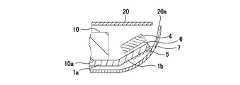
[他の構成5]
また、コイルモジュール1は、図9に示すように、内部構造物10と重畳しない張出部1bが、電子機器の筐体20の側壁20aや他の構成部品等の形状に応じて、折り曲げるようにしてもよい。たとえば、コイルモジュール1は、筐体20の側壁20aが湾曲している場合、この側壁に応じて張出部1bを折り曲げることにより、省スペース化が図られた筐体20内に収納することができる。なお、張出部1bは、筐体20aの曲面に沿って円弧状(曲面状)に曲げてもよい。[Other configuration 5]
In addition, as shown in FIG. 9, the
[他の構成6]
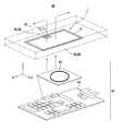
図10に示すように、スマートフォンのような電子機器の筐体20は、内面にコイルモジュール1が搭載される一方の筐体部材20bと、バッテリパックのバッテリ缶45やCPU等を含む本体の制御回路等が制御基板44上に搭載される他方の筐体部材20cとからなる。筐体20は、一方の筐体部材20bによって蓋をするようにして、バッテリ缶45等が含まれる筐体部材20cに結合させることによって構成される。筐体部材20b,20cは、互いにネジ止めや係合爪と係合孔と組合せ等周知の方法によって、取り外し可能に結合される。筐体部材20bには、コイルモジュール1のほかに、カメラモジュール等他の機能モジュールがあらかじめ単一であるいは複合して搭載されていてもよい。コイルモジュール1等の機能モジュールが搭載された筐体部材20bは、スマートフォン等の電子機器のユーザによって、筐体部材20cから取り外されて、他の機能モジュールを搭載する筐体部材が取り付けられるようにしてもよい。[Other configuration 6]
As shown in FIG. 10, a
筐体部材20bは、電子機器自体で美観を呈するようなデザイン上の目的や筐体の薄型化による強度不足を補うために、マグネシウム合金等の金属材料と樹脂材料とを複合的に組み合わせた複合材料によって形成される場合が増えている。すなわち、筐体部材20bは、金属材料からなるメタルカバー21aと、樹脂材料からなる樹脂部分21bとを含んでいる。 The
蓋状に用いられる筐体部材20bには、コイルモジュール1があらかじめ搭載されており、コイルモジュール1は、アンテナコイル5を含む面が、筐体部材20bを介してリーダライタに対向するように配置される。好ましくは、コイルモジュール1は、筐体部材20bの外周壁付近に配置される。図10に示すように、アンテナコイル5の一部が、筐体部材20bを構成するメタルカバー21aを覆うように配置される。アンテナコイル5は、メタルカバー21aの端部が、アンテナコイル5の中心Cに近接するように配置されるのが好ましい。 A
上述のように、コイルモジュール1を配置することによって、アンテナコイル5の中心C付近(図中のD円内)の磁界の強度が強まり、コイルモジュール1上の磁性シート4に磁界が導かれることになる。これによって、通信特性を安定させることができる。 As described above, by arranging the
図11(A)に示すように、通信特性をより安定させるために、磁性シート4は、アンテナコイル5の中心Cよりも、金属部分21a側に延設されるようにしてもよい。図11(B)に示すように、磁性シート4をアンテナコイル5の中心Cよりもさらに金属部分21a側に延設することによって、より安定した通信特性を得ることができる。なお、アンテナコイル5が図8のように、他方の筐体側にある場合おいても、磁性シート4の位置を延設させることによって、より安定した通信特性を実現できる。また、図9のように、張出部1bを筐体の側壁の形状に応じて折り曲げたり、曲面状に加工してもよいのは言うまでもない。また、基材の強度や美観の向上を図るために、筐体部材20bの全体の基材を樹脂等により形成し、その内面、あるいは外面を金属コートすることによってメタルカバーを構成してもよい。そのような場合についても同様に、アンテナコイル5の一部が、メタルカバー21aの一部を覆うように配置される。 As shown in FIG. 11A, the
[近距離無線通信システム]
次に、コイルモジュール1による近距離無線通信機能について説明する。たとえば図12に示すように、コイルモジュール1は、たとえば携帯電話機30の筐体20内部に組み込まれ、コイルモジュール1は、RFID用の無線通信システム40として使用される。[Near field communication system]
Next, the short-range wireless communication function by the
無線通信システム40は、リーダライタ41が、コイルモジュール1とともに携帯電話機30に組み込まれたメモリモジュール42に対してアクセスするものである。ここで、コイルモジュール1とリーダライタ41とは、三次元直交座標系xyzのxy平面において互いに対向するように配置されているものとする。 In the
リーダライタ41は、xy平面において互いに対向するコイルモジュール1のアンテナコイル5に対して、z軸方向に磁界を発信する発信器として機能し、具体的には、アンテナコイル5に向けて磁界を発信するアンテナ43と、メモリモジュール42と通信を行う制御基板44とを備える。 The reader /
すなわち、リーダライタ41は、アンテナ43と電気的に接続された制御基板44が配設されている。この制御基板44には、一又は複数の集積回路チップ等の電子部品からなる制御回路が実装されている。この制御回路は、アンテナコイル5を介してメモリモジュール42から受信されたデータに基づいて、各種の処理を実行する。たとえば、制御回路は、メモリモジュール42に対してデータを送信する場合、データを符号化し、符号化したデータに基づいて、所定の周波数(たとえば、13.56MHz)の搬送波を変調し、変調した変調信号を増幅し、増幅した変調信号でアンテナ43を駆動する。また、制御回路は、メモリモジュール42からデータを読み出す場合、アンテナ43で受信されたデータの変調信号を増幅し、増幅したデータの変調信号を復調し、復調したデータを復号する。なお、制御回路では、一般的なリーダライタで用いられる符号化方式及び変調方式が用いられ、たとえば、マンチェスタ符号化方式やASK(Amplitude Shift Keying)変調方式が用いられている。 That is, the reader /
コイルモジュール1は、アンテナコイル5が、リーダライタ41から発信される磁界を受けリーダライタ41と誘導結合して、携帯電話機30に組み込まれた記憶媒体であるメモリモジュール42に信号を供給する。 In the
アンテナコイル5は、リーダライタ41から発信される磁界を受けると、リーダライタ41と誘導結合によって磁気的に結合され、変調された電磁波を受信して、端子部8a、8bを介して受信信号をメモリモジュール42に供給する。 When the
メモリモジュール42は、アンテナコイル5に流れる電流により駆動し、リーダライタ41との間で通信を行う。具体的に、メモリモジュール42は、受信された変調信号を復調し、復調したデータを復号して、復号したデータを、当該メモリモジュール42が有する内部メモリに書き込む。また、メモリモジュール42は、リーダライタ41に送信するデータを内部メモリから読み出し、読み出したデータを符号化し、符号化したデータに基づいて搬送波を変調し、誘導結合によって磁気的に結合されたアンテナコイル5を介して変調された電波をリーダライタ41に送信する。 The
以上、本発明に係るコイルモジュール1として、RFID用のアンテナモジュールに適用した場合を例に説明したが、本発明は、RFID用のアンテナモジュールの他にも、たとえばQi等の非接触充電用のモジュールやその他のアンテナモジュールに適用してもよい。 As described above, the case where the
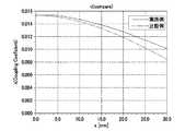
次いで、本発明が適用されたコイルモジュール1と従来のコイルモジュールとを比較した実施例について説明する。実施例及び比較例ともに、図13及び図14に示すように、コイルモジュールをリーダライタに対向させて配置し、徐々にリーダライタを図13及び図14中矢印Y軸方向へ移動させたときの結合係数k値の変化をシミュレーションで求めた。 Next, an embodiment in which the
<比較例>
比較例に係るアンテナ装置では、図13に示すように、コイルモジュール50の全体を金属製のバッテリ缶45の主面部45aに重畳させるとともに、コイルモジュール50とリーダライタ41とを対向させて、リーダライタ41とコイルモジュール50との相対的な位置関係を変化させたときの通信特性について評価した。<Comparative example>
In the antenna device according to the comparative example, as shown in FIG. 13, the
具体的な評価条件としては、次のようにした。すなわち、リーダライタ41のアンテナ43は、XY軸方向で規定される外形が70mm×70mmで1.5mmピッチの2巻コイルとした。また、バッテリ缶45はXYZ軸方向で規定される寸法が60mm×50mm×5mmのアルミブロックとした。コイルモジュール50のアンテナコイル51は、XY軸方向で規定される外形が50mm×40mmで1mmピッチの4巻のコイルである。コイルモジュール50の磁性シート52は、非透磁率120で、厚さ0.2mmのフェライトシートを保護フィルムで覆ったものを用い、アンテナコイル51の全面に亘って接着剤層を介して接着した。 Specific evaluation conditions were as follows. That is, the
バッテリ缶45の主面部45aとアンテナコイル51との距離は0.5mmである。さらに、Z軸方向で規定される、リーダライタ41のアンテナ43からアンテナコイル51までの距離は40mmとした。そして、電子機器筐体に見立てたステンレス製の補強プレート53の上に、バッテリ缶45、コイルモジュール50を、この順で重畳させた。 The distance between the
ここで、リーダライタ41とアンテナコイル51との相対的な位置関係を示す値として、次のaを用いた。すなわち、aは、リーダライタ41のアンテナ43の中心を通るZ軸方向の軸線43aとアンテナコイル51の中心を通るZ軸方向の軸線51aとを想定したときに、両軸線43a,51aが一致した位置から、図13中矢印Y軸方向にリーダライタ41を移動させたときの、両軸線43a,51a間の距離である。 Here, the following a is used as a value indicating the relative positional relationship between the reader /
以上のような条件の下、aの値を0mmから30mmまで変化させたときの、アンテナコイル51の結合係数をシミュレーションで求めた。結合係数の変化を図15に示す。 Under the above conditions, the coupling coefficient of the
<実施例>
本実施例では、図14に示すように、金属製のバッテリ缶45と重畳する重畳部1aとバッテリ缶45の一側縁より外方に張り出す張出部1bとを備えたコイルモジュール1を用いた。張出部1bにはアンテナコイル5の一部が形成されるとともに、磁性シート4が貼着されている。そして、本実施例においても、コイルモジュール1とリーダライタ41とを対向させて、リーダライタ41とコイルモジュール1との相対的な位置関係を変化させたときの通信特性について評価した。<Example>
In the present embodiment, as shown in FIG. 14, the
具体的な評価条件は、リーダライタ41、バッテリ缶45、補強プレート53、リーダライタ41のアンテナ43からアンテナコイル5までの距離については、上述した比較例と同じである。コイルモジュール1のアンテナコイル5は、比較例に係るアンテナコイル51と略同面積となるように、XY軸方向で規定される外形が33.3mm×60mmで1.5mmピッチの2巻コイルとした。磁性シート4は、比較例に係る磁性シート52と同じ非透磁率120で、厚さ0.2mmのフェライトシートを保護フィルムで覆ったものを用い、コイルモジュール1の張出部1bに接着剤層を介して接着した。実施例に係る磁性シート4は、比較例に係る磁性シート52に比して、フェライトの使用量を20%に削減している。 Specific evaluation conditions are the same as those in the comparative example described above with respect to the reader /
実施例においては、バッテリ缶45と重畳する重畳部1aに磁性シート4が設けられていないため、バッテリ缶45の主面部45aとアンテナコイル5との距離は0.1mmである。すなわち、実施例の構成によれば、比較例の構成に比して、バッテリ缶45の厚さ方向に0.4mmの薄型化が図られたこととなる。これは、実施例によれば、比較例に比して、磁性シート4の厚さに加え、磁性シート4を保護する保護フィルムや、磁性シート4を貼着する接着剤層の厚さも削減できたことによる。 In the embodiment, since the
また、実施例では、電子機器筐体に見立てたステンレス製の補強プレート53の上に、バッテリ缶45、コイルモジュール1を、この順で重畳させた。リーダライタ41とアンテナコイル5との相対的な位置関係を示す値としては、比較例と同様に、リーダライタ41のアンテナ43の中心を通るZ軸方向の軸線43aとアンテナコイル5の中心を通るZ軸方向の軸線5aとを想定したときに、両軸線43a,5aが一致した位置から、図14中矢印Y軸方向にリーダライタ41を移動させたときの、両軸線43a,5a間の距離aを用いた。 In the embodiment, the battery can 45 and the
以上のような条件の下、aの値を0mmから30mmまで変化させたときの、アンテナコイル5の結合係数をシミュレーションで求めた。結合係数の変化を図16に示す。実施例によれば、比較例に比して結合係数が向上されていることが分かる。これは、アンテナコイル5の長手方向にリーダライタ41を移動させている点で、アンテナコイル51の短手方向にリーダライタ41を移動させている比較例に比して、実施例は有利であることにもよるが、少なくとも実施例は比較例と同等以上の結合係数を有するといえる。 Under the above conditions, the coupling coefficient of the
すなわち、実施例に係る構成によれば、コイルモジュールの特性を損なうことなく、バッテリ缶45の厚さ方向に薄型化を図ることができ、狭小化されたスペースにも搭載可能なコイルモジュールを用いた電子機器を提供することができる。 That is, according to the configuration according to the embodiment, the coil module can be thinned in the thickness direction of the battery can 45 without impairing the characteristics of the coil module, and can be mounted in a narrow space. Can be provided.
1 コイルモジュール、1a 重畳部、1b 張出部、4 磁性シート、5 アンテナコイル、6 接着剤層、7 フレキシブル基板、10 内部構造物、10a 主面部、10b 端部、20 電子機器筐体、11 金属箔、11a 接着剤層、11b 高導電率金属、11c 絶縁層、11d 端部、20a 側壁、20b,20c 筐体部材、21a メタルカバー、21b 樹脂部分、30 携帯電話機、40 無線通信システム、41 リーダライタ、42 メモリモジュール、43 アンテナ、44 制御基板、45 バッテリ缶、45a 主面部DESCRIPTION OF
Claims (16)
Translated fromJapanese上記コイルモジュールは、上記ループコイルの一部が筐体の内部構造物と重畳されるとともに、上記磁性シートが、上記ループコイルの上記内部構造物と重畳する面側の上記内部構造物と重畳しない位置に設けられ、
上記内部構造物は、一部又は全部が金属体である、
電子機器。A coil module having a loop coil wound in a planar shape and a sheet-like magnetic sheet formed of a magnetic material and overlapping at least a part of the loop coil;
In the coil module, a part of the loop coil is overlapped with the internal structure of the casing, and the magnetic sheet is not overlapped with the internal structure on a surface side overlapping the internal structure of the loop coil. In place,
The internal structure is part or all of a metal body.
Electronics.
上記ループコイルの一部に重畳する導電体とを備え、
上記磁性シートは、上記導電体と重畳する上記ループコイルの面とは反対側で該導電体と重畳しない位置に設けられている電子機器。A coil module including a loop coil wound in a planar shape and a sheet-like magnetic sheet formed of a magnetic material and overlapping at least a part of the loop coil;
A conductor superposed on a part of the loop coil,
The electronic device is provided in a position where the magnetic sheet is not overlapped with the conductor on the side opposite to the surface of the loop coil overlapping with the conductor.
上記内部構造物は、一部又は全部が金属体である、請求項6記載の電子機器The conductor is partially overlapped or connected to the internal structure of the housing,
The electronic device according to claim6, wherein a part or all of the internal structure is a metal body.
上記磁性シートは、上記ループコイルの上記一方側及び/又は他方側と重畳する請求項6記載の電子機器。In the coil module, one side and / or the other side through the center of the loop coil is formed at a position that does not overlap the conductor.
The electronic device according to claim6 , wherein the magnetic sheet overlaps with the one side and / or the other side of the loop coil.
面状に巻回されたループコイルと、磁性材料により形成され、該ループコイルの少なくとも一部と重畳するシート状の磁性シートとを有し、上記電子機器の筐体を構成する一方の部材の内面に設けられたコイルモジュールと、
上記一方の部材の一部を構成する導電体とを備え、
上記コイルモジュールは、上記ループコイルの一部が上記導電体と重畳されるとともに、上記磁性シートが、該導電体と重畳する該ループコイルの面側とは反対側で該導電体と重畳しない位置に設けられているアンテナ装置。In an antenna device incorporated in an electronic device and communicating with an external device via an electromagnetic field signal,
A loop coil wound in a planar shape, and a sheet-like magnetic sheet formed of a magnetic material and overlapping at least a part of the loop coil, and one member constituting the casing of the electronic device A coil module provided on the inner surface;
A conductor constituting a part of the one member,
The coil module is configured such that a part of the loop coil is overlapped with the conductor, and the magnetic sheet is not overlapped with the conductor on the opposite side of the surface of the loop coil that is overlapped with the conductor. Antenna device provided in
Priority Applications (7)
| Application Number | Priority Date | Filing Date | Title |
|---|---|---|---|
| JP2013021617AJP6143485B2 (en) | 2012-10-17 | 2013-02-06 | Electronic device and antenna device |
| KR1020157012936AKR102067517B1 (en) | 2012-10-17 | 2013-10-16 | Electronic device and antenna device |
| EP13846675.0AEP2911243B1 (en) | 2012-10-17 | 2013-10-16 | Electronic device and antenna device |
| PCT/JP2013/078086WO2014061704A1 (en) | 2012-10-17 | 2013-10-16 | Electronic device and antenna device |
| US14/436,413US10236557B2 (en) | 2012-10-17 | 2013-10-16 | Electronic device and antenna device |
| CN201380054451.7ACN104737371B (en) | 2012-10-17 | 2013-10-16 | Electronic equipment and antenna assembly |
| TW102137467ATWI611632B (en) | 2012-10-17 | 2013-10-17 | Electronic equipment and antenna device |
Applications Claiming Priority (3)
| Application Number | Priority Date | Filing Date | Title |
|---|---|---|---|
| JP2012230266 | 2012-10-17 | ||
| JP2012230266 | 2012-10-17 | ||
| JP2013021617AJP6143485B2 (en) | 2012-10-17 | 2013-02-06 | Electronic device and antenna device |
Publications (2)
| Publication Number | Publication Date |
|---|---|
| JP2014099833A JP2014099833A (en) | 2014-05-29 |
| JP6143485B2true JP6143485B2 (en) | 2017-06-07 |
Family
ID=50488265
Family Applications (1)
| Application Number | Title | Priority Date | Filing Date |
|---|---|---|---|
| JP2013021617AActiveJP6143485B2 (en) | 2012-10-17 | 2013-02-06 | Electronic device and antenna device |
Country Status (7)
| Country | Link |
|---|---|
| US (1) | US10236557B2 (en) |
| EP (1) | EP2911243B1 (en) |
| JP (1) | JP6143485B2 (en) |
| KR (1) | KR102067517B1 (en) |
| CN (1) | CN104737371B (en) |
| TW (1) | TWI611632B (en) |
| WO (1) | WO2014061704A1 (en) |
Families Citing this family (7)
| Publication number | Priority date | Publication date | Assignee | Title |
|---|---|---|---|---|
| US9369185B2 (en)* | 2013-10-28 | 2016-06-14 | Stmicroelectronics, Inc. | Method and apparatus for inductive coupling utilizing an amorphous metal barrier |
| KR101762778B1 (en) | 2014-03-04 | 2017-07-28 | 엘지이노텍 주식회사 | Wireless communication and charge substrate and wireless communication and charge device |
| US10090592B2 (en)* | 2015-10-29 | 2018-10-02 | Sonitus Technologies Inc. | Communication device |
| JP2020031246A (en)* | 2016-11-10 | 2020-02-27 | 株式会社村田製作所 | Communication terminal |
| CN110832959B (en)* | 2017-07-07 | 2020-11-24 | 株式会社村田制作所 | High-frequency power circuit module |
| KR102388342B1 (en)* | 2017-09-07 | 2022-04-20 | 삼성전자주식회사 | An electronic device comprising antenna |
| CN116053782A (en)* | 2021-04-19 | 2023-05-02 | 荣耀终端有限公司 | Electronic equipment |
Family Cites Families (18)
| Publication number | Priority date | Publication date | Assignee | Title |
|---|---|---|---|---|
| TW531976B (en)* | 2001-01-11 | 2003-05-11 | Hanex Co Ltd | Communication apparatus and installing structure, manufacturing method and communication method |
| EP1439608A4 (en) | 2001-09-28 | 2008-02-06 | Mitsubishi Materials Corp | Antenna coil and rfid-use tag using it, transponder-use antenna |
| JP3896965B2 (en)* | 2002-01-17 | 2007-03-22 | 三菱マテリアル株式会社 | Reader / writer antenna and reader / writer equipped with the antenna |
| JP4273314B2 (en)* | 2003-08-27 | 2009-06-03 | 三菱マテリアル株式会社 | RFID tag and manufacturing method thereof |
| JP2006113944A (en)* | 2004-10-18 | 2006-04-27 | Hanex Co Ltd | Data carrier structure and its installation structure |
| JP3933191B1 (en) | 2006-03-13 | 2007-06-20 | 株式会社村田製作所 | Portable electronic devices |
| US7762472B2 (en) | 2007-07-04 | 2010-07-27 | Murata Manufacturing Co., Ltd | Wireless IC device |
| US8235299B2 (en) | 2007-07-04 | 2012-08-07 | Murata Manufacturing Co., Ltd. | Wireless IC device and component for wireless IC device |
| EP3364501A1 (en)* | 2007-07-04 | 2018-08-22 | Murata Manufacturing Co., Ltd. | Wireless ic device and component for wireless ic device |
| JP4978657B2 (en)* | 2009-05-08 | 2012-07-18 | 株式会社村田製作所 | Antenna device |
| EP3057178A1 (en)* | 2009-09-25 | 2016-08-17 | Murata Manufacturing Co., Ltd. | Antenna device and mobile terminal |
| GB2488450B (en)* | 2009-12-24 | 2014-08-20 | Murata Manufacturing Co | Antenna and mobile terminal |
| CN102474000B (en)* | 2009-12-24 | 2015-07-22 | 株式会社村田制作所 | Antenna and Portable Terminal |
| JP5135450B2 (en) | 2010-03-31 | 2013-02-06 | デクセリアルズ株式会社 | Antenna device, communication device |
| WO2012050037A1 (en)* | 2010-10-12 | 2012-04-19 | 株式会社村田製作所 | Antenna apparatus and communication terminal apparatus |
| JP5848120B2 (en) | 2010-12-28 | 2016-01-27 | デクセリアルズ株式会社 | ANTENNA MODULE, COMMUNICATION DEVICE, AND ANTENNA MODULE MANUFACTURING METHOD |
| CN104638342B (en)* | 2011-11-09 | 2018-02-09 | 株式会社村田制作所 | Antenna assembly and electronic equipment |
| CN202434688U (en)* | 2011-12-20 | 2012-09-12 | 瑞声声学科技(常州)有限公司 | Near-field communication antenna |
- 2013
- 2013-02-06JPJP2013021617Apatent/JP6143485B2/enactiveActive
- 2013-10-16KRKR1020157012936Apatent/KR102067517B1/enactiveActive
- 2013-10-16EPEP13846675.0Apatent/EP2911243B1/enactiveActive
- 2013-10-16CNCN201380054451.7Apatent/CN104737371B/enactiveActive
- 2013-10-16WOPCT/JP2013/078086patent/WO2014061704A1/enactiveApplication Filing
- 2013-10-16USUS14/436,413patent/US10236557B2/enactiveActive
- 2013-10-17TWTW102137467Apatent/TWI611632B/enactive
Also Published As
| Publication number | Publication date |
|---|---|
| JP2014099833A (en) | 2014-05-29 |
| KR20150070361A (en) | 2015-06-24 |
| TWI611632B (en) | 2018-01-11 |
| WO2014061704A1 (en) | 2014-04-24 |
| CN104737371A (en) | 2015-06-24 |
| US10236557B2 (en) | 2019-03-19 |
| EP2911243A4 (en) | 2016-06-08 |
| US20150288054A1 (en) | 2015-10-08 |
| EP2911243B1 (en) | 2024-04-03 |
| KR102067517B1 (en) | 2020-02-11 |
| CN104737371B (en) | 2018-03-30 |
| TW201417403A (en) | 2014-05-01 |
| EP2911243A1 (en) | 2015-08-26 |
Similar Documents
| Publication | Publication Date | Title |
|---|---|---|
| JP6034644B2 (en) | Composite coil module and portable device | |
| TWI618298B (en) | Composite coil module and electronic machine | |
| JP6110656B2 (en) | Wireless communication system, antenna module, and electronic device | |
| JP6143485B2 (en) | Electronic device and antenna device | |
| JP6099352B2 (en) | Electronic device and coil module | |
| JP6223067B2 (en) | Electronics |
Legal Events
| Date | Code | Title | Description |
|---|---|---|---|
| RD03 | Notification of appointment of power of attorney | Free format text:JAPANESE INTERMEDIATE CODE: A7423 Effective date:20151111 | |
| A621 | Written request for application examination | Free format text:JAPANESE INTERMEDIATE CODE: A621 Effective date:20160112 | |
| A131 | Notification of reasons for refusal | Free format text:JAPANESE INTERMEDIATE CODE: A131 Effective date:20161025 | |
| A521 | Request for written amendment filed | Free format text:JAPANESE INTERMEDIATE CODE: A523 Effective date:20161215 | |
| TRDD | Decision of grant or rejection written | ||
| A01 | Written decision to grant a patent or to grant a registration (utility model) | Free format text:JAPANESE INTERMEDIATE CODE: A01 Effective date:20170418 | |
| A61 | First payment of annual fees (during grant procedure) | Free format text:JAPANESE INTERMEDIATE CODE: A61 Effective date:20170509 | |
| R150 | Certificate of patent or registration of utility model | Ref document number:6143485 Country of ref document:JP Free format text:JAPANESE INTERMEDIATE CODE: R150 | |
| R250 | Receipt of annual fees | Free format text:JAPANESE INTERMEDIATE CODE: R250 | |
| R250 | Receipt of annual fees | Free format text:JAPANESE INTERMEDIATE CODE: R250 | |
| R250 | Receipt of annual fees | Free format text:JAPANESE INTERMEDIATE CODE: R250 | |
| R250 | Receipt of annual fees | Free format text:JAPANESE INTERMEDIATE CODE: R250 | |
| R250 | Receipt of annual fees | Free format text:JAPANESE INTERMEDIATE CODE: R250 | |
| R250 | Receipt of annual fees | Free format text:JAPANESE INTERMEDIATE CODE: R250 |