JP6135840B2 - LASER DEVICE AND METHOD FOR MANUFACTURING LASER DEVICE - Google Patents
LASER DEVICE AND METHOD FOR MANUFACTURING LASER DEVICEDownload PDFInfo
- Publication number
- JP6135840B2 JP6135840B2JP2012195896AJP2012195896AJP6135840B2JP 6135840 B2JP6135840 B2JP 6135840B2JP 2012195896 AJP2012195896 AJP 2012195896AJP 2012195896 AJP2012195896 AJP 2012195896AJP 6135840 B2JP6135840 B2JP 6135840B2
- Authority
- JP
- Japan
- Prior art keywords
- holder
- laser
- incident
- shaping lens
- emission
- Prior art date
- Legal status (The legal status is an assumption and is not a legal conclusion. Google has not performed a legal analysis and makes no representation as to the accuracy of the status listed.)
- Active
Links
Images


Landscapes
- Semiconductor Lasers (AREA)
Description
Translated fromJapanese本発明は、半導体レーザと複数の光学素子により構成されたレーザ装置及びレーザ装置の製造方法に関する。 The present invention relates to a laser device including a semiconductor laser and a plurality of optical elements, and a method for manufacturing the laser device.
レーザ装置に用いられる各種の光学素子は、光学調整を行った後に様々な手法によって固定される。光学調整には、例えば、ミラーで反射させるレーザ光の角度を摺動により調整する方法などが提案されている(例えば特許文献1参照。)。また、接着剤や止めネジを用いたり、光学素子を保持する金属ホルダをレーザ溶接や半田付けしたりすることによって、光学素子が固定される。例えば、波長安定化レーザについて、光学素子の一部として光ファイバに回折格子を形成したファイバーブラッググレーティング(FBG)が使用され、FBGを保持する金属ホルダが半田付けやレーザ溶接を用いて固定される。 Various optical elements used in the laser device are fixed by various methods after optical adjustment. For optical adjustment, for example, a method of adjusting the angle of laser light reflected by a mirror by sliding has been proposed (see, for example, Patent Document 1). Further, the optical element is fixed by using an adhesive or a set screw, or by laser welding or soldering a metal holder for holding the optical element. For example, for a wavelength stabilized laser, a fiber Bragg grating (FBG) in which a diffraction grating is formed on an optical fiber is used as a part of an optical element, and a metal holder that holds the FBG is fixed by soldering or laser welding. .
透過型グレーティング素子を用いて半導体レーザと外部共振器を構成する場合には、光学調整を行う調整機構と光学素子の固定方法が重要である。例えば、整形レンズ、透過型グレーティング素子などについてそれぞれ光学調整を行い、これらを接着剤、溶接、止めネジなどにより固定する。 When a semiconductor laser and an external resonator are configured using a transmissive grating element, an adjustment mechanism that performs optical adjustment and an optical element fixing method are important. For example, optical adjustment is performed for each of the shaping lens, the transmission type grating element, and the like, and these are fixed by an adhesive, welding, a set screw, or the like.
光学調整に関しては、それぞれの光学素子を独立に調整することで、レーザ光整形調整や外部共振器調整の自由度が増し、製造性もよい。しかし、部品点数が増えたり、装置が大きくなったりする。 Regarding optical adjustment, by independently adjusting each optical element, the degree of freedom of laser beam shaping adjustment and external resonator adjustment is increased, and manufacturability is also good. However, the number of parts increases and the apparatus becomes large.
光学素子の固定方法に関しては、接着剤による固定は、リードタイムの増加、アウトガスの発生、強度などの長期信頼性などについて問題がある。止めネジによる固定は、光学素子への応力、強度、振動時の信頼性などに問題が生じる可能性がある。 Regarding the fixing method of the optical element, fixing with an adhesive has problems in terms of increase in lead time, generation of outgas, long-term reliability such as strength, and the like. Fixing with a set screw may cause problems in stress, strength, reliability during vibration, etc. to the optical element.
これらに対し、レーザ溶接による固定は、接着剤による固定におけるアウトガスの発生がなく、硬化時間も必要ない。更に、強度的に問題がなく、長期信頼性を確保できる。しかし、レーザ溶接による固定には、溶接出力の大きさや光学素子の形状にもよるが、溶接歪みによる光学素子の位置変動や溶接中に飛散するスラグや微粒子粒などの溶接スパッタによる光学素子への汚染が生じる恐れがある。 On the other hand, fixing by laser welding does not generate outgas in fixing by an adhesive and does not require curing time. Furthermore, there is no problem in strength, and long-term reliability can be ensured. However, fixing by laser welding depends on the size of the welding output and the shape of the optical element. However, the position of the optical element varies due to welding distortion, and the optical element due to welding spatter such as slag and fine particles scattered during welding. Contamination may occur.
例えば波長安定化レーザ装置に関しては、利用分野が多岐にわたり、様々な条件下で使用され、また、最近の多波長、高出力化によってレーザ光源として使用される半導体レーザに準ずるサイズ、信頼性、価格が求められている。このため、レーザ装置の長期信頼性の確保、歩留まり低下の抑制が必須である。 For example, the wavelength-stabilized laser device has a wide range of fields of application and is used under various conditions. Also, the size, reliability, and price are the same as those of semiconductor lasers that are used as laser light sources due to the recent multi-wavelength and high output. Is required. For this reason, it is essential to ensure long-term reliability of the laser device and to suppress a decrease in yield.
本発明は、光学素子がレーザ溶接によって固定された、長期信頼性が確保され、且つ歩留まりの低下が抑制されたレーザ装置及びレーザ装置の製造方法を提供することを目的とする。 An object of the present invention is to provide a laser device in which an optical element is fixed by laser welding, long-term reliability is ensured, and a decrease in yield is suppressed, and a method for manufacturing the laser device.
本発明の一態様によれば、(イ)レーザ光を出射する半導体レーザと、(ロ)半導体レーザが内部に保持された管形状の第1のホルダと、(ハ)レーザ光を整形する整形レンズと、(ニ)整形レンズが内部に保持された管形状であって、レーザ光が入射する入射口が形成された入射面、及び整形レンズを透過したレーザ光が出射する出射口が形成され、且つ出射口周囲の外縁部が球面形状である出射面を有し、入射面の外周部が第1のホルダにレーザ溶接された第2のホルダと、(ホ)整形レンズを透過したレーザ光が入射される透過型グレーティング素子と、(ヘ)透過型グレーティング素子が内部に保持された管形状であって、レーザ光が入射される入射開口部が、第2のホルダの出射口の周囲を覆うように球面形状の外縁部に線接触して、第2のホルダにレーザ溶接された第3のホルダとを備え、第3のホルダの入射開口部に外側よりも内側が低く形成された段差が外周に沿って配置され、段差の2つの角部において第2のホルダの出射面の外縁部に第3のホルダが互いに離間した2つの円周線で線接触接し、2つの円周線のうちの外側の円周線において第2のホルダと第3のホルダがレーザ溶接されているレーザ装置が提供される。According to one aspect of the present invention, (b) a semiconductor laser that emits laser light, (b) a tube-shaped first holder in which the semiconductor laser is held, and (c) shaping that shapes the laser light. A lens, and (d) a tube shape in which a shaping lens is held inside, an incident surface on which an incident port through which laser light is incident is formed, and an exit port from which laser light that has passed through the shaping lens is emitted. And a second holder in which an outer edge portion around the emission port has a spherical emission surface, and an outer peripheral portion of the incident surface is laser-welded to the first holder, and (e) laser light transmitted through the shaping lens And (f) a tube shape in which the transmissive grating element is held inside, and an incident opening portion into which the laser beam is incident is provided around the emission port of the second holder. Line contact with the outer edge of the spherical shape to cover , And a third holder is laser welded to a secondholder, a step in which the inner is formed lower than the outside entrance aperture of the third holder are arranged along the outer circumference, the two corners of the step The third holder is in line-contact contact with two outer circumferential lines spaced from each other at the outer edge of the emission surface of the second holder, and the second holder is connected to the outer circumference of the two circumferential lines. A laser device is provided in whichthe third holder is laser welded .
本発明の他の態様によれば、(イ)半導体レーザを内部に保持する第1のホルダを準備するステップと、(ロ)整形レンズを内部に保持し、半導体レーザから出射されるレーザ光が入射される入射口が形成された入射面と、整形レンズを透過したレーザ光が出射する出射口が形成され、且つ出射口周囲の外縁部が球面形状である出射面とを有する第2のホルダを準備し、第1のホルダに第2のホルダを連結するステップと、(ハ)整形レンズの光学調整を行った後、入射面の外周部を第1のホルダにレーザ溶接することによって第2のホルダを第1のホルダに固定するステップと、(ニ)透過型グレーティング素子を内部に保持し、レーザ光が入射される入射開口部に外側よりも内側が低く形成された段差が外周に沿って配置された環形状の第3のホルダを準備し、第3のホルダの入射開口部を第2のホルダの出射口の周囲を覆うように球面形状の外縁部に線接触させるステップと、(ホ)第2のホルダに線接触した状態で第3のホルダを摺動させて外部共振器調整を行った後、第2のホルダの外縁部に第3のホルダの入射開口部をレーザ溶接することによって第3のホルダを第2のホルダに固定するステップとを含み、第2のホルダの出射面の外縁部に第3のホルダの段差の2つの角部を接触させることにより、第2のホルダと第3のホルダを互いに離間した2つの円周線で線接触させ、2つの円周線のうちの外側の円周線において第2のホルダと第3のホルダをレーザ溶接するレーザ装置の製造方法が提供される。According to another aspect of the present invention, (b) a step of preparing a first holder for holding the semiconductor laser therein; and (b) a laser beam emitted from the semiconductor laser holding the shaping lens inside. A second holder having an incident surface on which an incident port is formed and an exit surface on which an exit port from which laser light transmitted through the shaping lens is emitted is formed and an outer edge portion around the exit port is spherical. And (2) connecting the second holder to the first holder, and (c) performing optical adjustment of the shaping lens, and then laser welding the outer peripheral portion of the incident surface to the first holder. A step of fixing the holder to the first holder, and (d)a step formed by holding the transmissive grating element inside andforming the laser beam incident on theinner side lower than the outer side along the outer periphery. It has been ring-shaped arrangement Te 3 is prepared, and a step of bringing the incident opening of the third holder into line contact with the outer peripheral portion of the spherical shape so as to cover the periphery of the exit of the second holder; After adjusting the external resonator by sliding the third holder in contact with the third holder, the third holder is attached to the outer edge of the second holder by laser welding the incident opening of the third holder. and securing the second holderseen including, by contacting the two corners of the step of the third holder on the outer edge of the exit surface of the second holder, the second holder and a third holder A method of manufacturinga laser device is provided inwhich line contact is made between two circumferential lines spaced apart from each other, and the second holder and the third holder are laser-welded on the outer circumferential line of the two circumferential lines .
本発明によれば、光学素子がレーザ溶接によって固定された、長期信頼性が確保され、且つ歩留まりの低下が抑制されたレーザ装置及びレーザ装置の製造方法を提供できる。 ADVANTAGE OF THE INVENTION According to this invention, the optical element was fixed by laser welding, long-term reliability was ensured, and the manufacturing method of a laser apparatus by which the fall of the yield was suppressed can be provided.
図面を参照して、本発明の実施形態を説明する。以下の図面の記載において、同一又は類似の部分には同一又は類似の符号を付している。ただし、図面は模式的なものであることに留意すべきである。又、以下に示す実施形態は、この発明の技術的思想を具体化するための装置や方法を例示するものであって、この発明の実施形態は、構成部品の構造、配置などを下記のものに特定するものでない。この発明の実施形態は、特許請求の範囲において、種々の変更を加えることができる。 Embodiments of the present invention will be described with reference to the drawings. In the following description of the drawings, the same or similar parts are denoted by the same or similar reference numerals. However, it should be noted that the drawings are schematic. Further, the embodiment described below exemplifies an apparatus and a method for embodying the technical idea of the present invention, and the embodiment of the present invention has the following structure and arrangement of components. It is not something specific. The embodiment of the present invention can be variously modified within the scope of the claims.
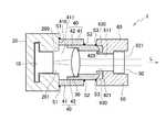
本発明の実施形態に係るレーザ装置1は、図1に示すように、レーザ光Lを出射する半導体レーザ10と、入射されたレーザ光Lを整形する整形レンズ30と、整形レンズ30を透過したレーザ光Lが入射される透過型グレーティング素子50とを備える。 As shown in FIG. 1, the
整形レンズ30によって、半導体レーザ10の出射するレーザ光Lの光径と出射方向が調整される。透過型グレーティング素子50は、入射されるレーザ光Lの一部を反射して半導体レーザ10との間で外部共振器を構成する。これにより、レーザ装置1はレーザ光Lの波長を狭帯域化、安定化する。 The shaping
透過型グレーティング素子50は、例えばボリュームブラッググレーティング(Volume Bragg Grating:VBG)やボリュームホログラフィックグレーティング(Volume Holographic Grating:VHG)などである。なお、半導体レーザ10との間で外部共振器を構成するために、透過型グレーティング素子50のレーザ光Lに対する反射率は、10%〜40%程度であることが好ましい。 The
半導体レーザ10は、管形状の第1のホルダ20の内部に保持される。第1のホルダ20は、例えば円筒形状である。半導体レーザ10から出射されたレーザ光Lは、出射開口部201から整形レンズ30に出射される
整形レンズ30は、管形状の第2のホルダ40の内部に保持される。第2のホルダ40は、レーザ光Lが入射する入射口411が形成された入射面410、及び入射口411に対向する出射口421が形成された出射面420を有する。そして、入射面410の外周部が、溶接照射箇所S1において第1のホルダ20にレーザ溶接されている。図1において、レーザ溶接光が照射されてレーザ溶接された箇所を黒丸「●」で示している(以下において同様。)。第2のホルダ40は、例えば円筒形状である。The
第2のホルダ40の入射面410から入射されて整形レンズ30を透過したレーザ光Lは、第2のホルダ40の出射面420に形成された出射口421から出射される。出射口421周囲の出射面420の外縁部は、外側に凸状の球面形状である。 The laser light L incident from the
透過型グレーティング素子50は、管形状の第3のホルダ60の内部に保持される。第3のホルダ60は、例えば円筒形状である。透過型グレーティング素子50を透過したレーザ光Lは、第3のホルダ60の出力開口部621から外部に出力される。 The
レーザ光Lが入射される第3のホルダ60の入射開口部611は、第2のホルダ40の出射口421の周囲を覆って出射面420の球面形状の外縁部に接している。そして、入射開口部611が出射面420に接する溶接照射箇所S3において、第3のホルダ60が第2のホルダ40にレーザ溶接されている。このため、第2のホルダ40の出射面420の先端部分が入射開口部611の内部に位置する状態で、第2のホルダ40に第3のホルダ60が固定されている。 The incident opening 611 of the
例えば、第2のホルダ40及び第3のホルダ60が円筒形状であり、第3のホルダ60と第2のホルダ40とは円周線で接触する。このとき、第3のホルダ60の入射開口部611の内径は、少なくとも第2のホルダ40と接触する領域において、第2のホルダ40の外径よりも小さい。 For example, the
図1に示したレーザ装置1では、半導体レーザ10から出射されて整形レンズ30及び透過型グレーティング素子50を経由したレーザ光Lが、所望の波長で安定して出力されるように各光学素子が光学調整されて、第1のホルダ20、第2のホルダ40及び第3のホルダ60が連結されている。図1において、レーザ光Lの光路を破線で示している。図1に示した例では、整形レンズ30は、半導体レーザ10から出射されたレーザ光Lを平行光とするためのコリメートレンズである。なお、第1のホルダ20、第2のホルダ40及び第3のホルダ60は、例えばステンレスやコバールなどの金属材料からなる。 In the
図1に示すように、第2のホルダ40は、入射側部41と出射側部42を有する。出射側部42の一部が入射側部41の内側に嵌め合わされた状態であり、出射側部42の嵌め合わされた部分の外壁が入射側部41に内接している。 As shown in FIG. 1, the
入射側部41は、一方の端部が入射面410である管形状であって、入射面410は溶接照射箇所S1において第1のホルダ20にレーザ溶接されている。入射面410に対向する入射側部41の他方の端部の外周部に、出射側部42の外部側面がレーザ溶接されている。これにより、入射側部41に出射側部42が固定されている。図1において、入射側部41と出射側部42との溶接箇所を溶接照射箇所S2として示している。 The
出射側部42は、一方の端部が出射面420である管形状であって、整形レンズ30が内部に保持されている。出射側部42の他方の端部は、入射側部41の内部に位置している。詳細は後述するが、入射側部41に出射側部42を固定する前は、レーザ光Lの光軸方向(以下において、単に「光軸方向」という。)に沿って出射側部42をスライドさせることにより、整形レンズ30の光軸方向の光学調整を行える。 The
図2に、第2のホルダ40の例を示す。図2に示すように、第2のホルダ40の出射面420は、レーザ光Lが通過する開口部である出射口421が中央領域に形成された球面形状である。 FIG. 2 shows an example of the
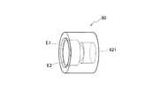
図1に示す第3のホルダ60では、入射開口部611に外側よりも内側が低く形成された段差が外周に沿って配置されている。入射開口部611に段差が形成されていることにより、段差の2つの角部において第2のホルダ40の出射面420の外縁部に第3のホルダ60が互いに離間した2つの円周線で接している。そして、外側の円周線において第2のホルダ40と第3のホルダ60がレーザ溶接されている。 In the
図3に、第3のホルダ60の例を示す。段差の角部E1、E2において、第3のホルダ60が第2のホルダ40の出射面420の球面形状部分に線接触する。そして、外側の角部E1において第3のホルダ60が第2のホルダ40にレーザ溶接される。 FIG. 3 shows an example of the
図1に示したレーザ装置1の製造方法の例を以下に説明する。 An example of a method for manufacturing the
先ず、半導体レーザ10を第1のホルダ20の内部に搭載する。そして、第1のホルダ20の出射開口部201の周囲を入射口411が覆うように、第1のホルダ20に第2のホルダ40を連結する。 First, the
第2のホルダ40は、半導体レーザ10から出射されるレーザ光Lのビーム調整を行えるように構成されている。即ち、第2のホルダ40は、光軸方向に垂直な方向(以下において「光軸垂直方向」という。)に位置が調整可能な入射側部41と、入射側部41に一部が嵌め合わされ、光軸方向の調整が行えるように位置を調整可能な出射側部42を有する。 The
具体的には、入射側部41を光軸垂直方向に動かして、光軸垂直方向に関して整形レンズ30の光学調整を行う。一方、出射側部42を入射側部41に対して光軸方向にスライドさせることによって、光軸方向に関して整形レンズ30の光学調整を行う。そして、入射面410の外周部を出射開口部201の周囲で第1のホルダ20にレーザ溶接する(溶接照射箇所S1)。これにより、入射側部41が第1のホルダ20に固定される。更に、入射面410である端部に対向する入射側部41の他方の端部の外周部と、出射側部42の外部側面とをレーザ溶接する(溶接照射箇所S2)。 Specifically, the
次いで、レーザ光Lの波長を狭帯域化、安定化するために、透過型グレーティング素子50を内部に保持した第3のホルダ60を第2のホルダ40に連結する。このとき、第3のホルダ60の入射開口部611の内径が、第2のホルダ40の出射面420の外径よりも小さく、且つ、出射口421の内径よりも大きい。このため、第3のホルダ60の入射開口部611が第2のホルダ40の出射口421の周囲を覆って、第2のホルダ40の球面形状の外縁部において第3のホルダ60が第2のホルダ40に線接触する。 Next, in order to narrow and stabilize the wavelength of the laser light L, the
第3のホルダ60と第2のホルダ40は円周線でのみ接触するため、摺動性よく自在に第2のホルダ40に対する第3のホルダ60の角度調整を行うことができる。このため、第2のホルダ40に対する第3のホルダ60の角度を調整することにより、半導体レーザ10と透過型グレーティング素子50との間で外部共振器を構成するように、透過型グレーティング素子50の光学調整を行うことができる。 Since the
第2のホルダ40に線接触させた状態の第3のホルダ60を摺動させて外部共振器調整を行った後、第2のホルダ40の出射面420の外縁部に第3のホルダ60の入射開口部611をレーザ溶接する(溶接照射箇所S3)。これにより、第3のホルダ60を第2のホルダ40に固定する。以上により、図1に示したレーザ装置1が完成する。 After adjusting the external resonator by sliding the
なお、図1に示した第3のホルダ60では、入射開口部611に外側よりも内側が低く形成された段差が外周に沿って配置されている。第2のホルダ40の出射面420の外縁部に第3のホルダ60の段差の2つの角部E1、E2を接触させることにより、第2のホルダ40と第3のホルダ60とは、互いに離間した2つの円周線で線接触する。そして、外側の円周線において第2のホルダ40と第3のホルダ60をレーザ溶接する。第3のホルダ60に形成される段差の大きさは、第2のホルダ40の出射面420の曲率の大きさに応じて設定される。 In the
一般的に、線接触の箇所にレーザ溶接を行うと、レーザ溶接光入射側の裏側にも溶接スパッタが飛散するおそれがある。このため、レーザ溶接による固定では、クリーニング作業の追加が必要になることがある。また、場合によっては第3のホルダ60内部の透過型グレーティング素子50が溶接スパッタによって汚染され、所定の特性が得られなかったり、歩留まりや長期信頼性が低下するなどの問題が生じたりする。 Generally, when laser welding is performed on a line contact portion, there is a possibility that welding spatter may be scattered on the back side of the laser welding light incident side. For this reason, the fixing by laser welding may require an additional cleaning operation. In some cases, the
しかしながら、図1に示したように第3のホルダ60の入射開口部611には段差が形成されている。第2のホルダ40と第3のホルダ60のレーザ溶接箇所の内部側の段差によって、発生した溶接スパッタを閉じ込めておくことができる。溶接スパッタが第3のホルダ60内部に飛散する場合は、溶接照射箇所S3を溶接するレーザ溶接光の光軸を延長した方向で溶接スパッタが内部に拡散される。このため、溶接スパッタを上記のように閉じ込める方法は効果的である。 However, as shown in FIG. 1, a step is formed in the incident opening 611 of the
或いは、レーザ溶接箇所と光学素子との間に溶接スパッタを塞き止める構造を採用するなどの、他の方法によって溶接スパッタが第3のホルダ60内部に飛散することを防止してもよい。 Alternatively, the welding spatter may be prevented from being scattered inside the
例えば図4に示すように、第3のホルダ60の入射開口部611の内側に、入射開口部611の外周に沿って溝630を形成する。第2のホルダ40と第3のホルダ60を連結すると、第2のホルダ40の出射面420の先端部分は溝630の内部に位置する。このとき、溝630の外側の縁を第2のホルダ40の出射面420の外縁部に環状に線接触させる。一方、溝630の内側の縁は、第2のホルダ40に接触させない。そして、溝630の外側の縁(溶接照射箇所S3)において第2のホルダ40と第3のホルダ60をレーザ溶接する。 For example, as shown in FIG. 4, a
図4に示した第3のホルダ60の構造を採用した場合、レーザ溶接箇所から第3のホルダ60の内部に飛散した溶接スパッタは、溝630の内壁に衝突し、そこで即座に冷却されて付着固定する。このため、透過型グレーティング素子50は溶接スパッタから保護される。なお、図4に示した構造を採用した場合にも、第3のホルダ60は第2のホルダ40に対して摺動性よく自在に角度調整を行える。 When the structure of the
上記のように、透過型グレーティング素子50が溶接スパッタによって汚染されないようにするためには、第2のホルダ40と第3のホルダ60とがレーザ溶接された溶接照射箇所S3と透過型グレーティング素子50とを結ぶ直線上に、溶接照射箇所S3から透過型グレーティング素子50を見通すことができないように第3のホルダ60内に遮蔽物が配置されていればよい。なお、レーザ溶接光の光軸上に位置し、且つ、レーザ光Lの光軸上に位置しないように遮蔽物が配置されるのはもちろんである。図3に示した例では、角部Eから外壁方向に延伸する面が遮蔽物として機能する。図4に示した例では、溝630の内壁が遮蔽物として機能する。 As described above, in order to prevent the transmission
また、図5に示すように、入射開口部611と透過型グレーティング素子50との間で、レーザ溶接光Wの光軸上に壁面が位置するように、第3のホルダ60の内壁の一部に凸部65を形成してもよい。凸部65の高さは、溶接照射箇所S3に照射されるレーザ溶接光Wの光軸方向に凸部65が位置するのに十分な高さであり、且つ、レーザ光Lが当たらない高さである。図5に示した構造を採用することによっても、第3のホルダ60内に浸入した溶接スパッタは凸部65に遮られるため、透過型グレーティング素子50が溶接スパッタによって汚染されることが防止される。 Further, as shown in FIG. 5, a part of the inner wall of the
ところで、第3のホルダ60の第2のホルダ40との接触部分を球面形状とすることによっても、溶接スパッタの内部飛散を抑制できる。しかし、この場合は、毎回の加工精度により球面形状部の接触状態が変わる。このため、外部共振器調整後の溶接歪みがどのように発生するかがわかりにくくなり、また、摩擦が不規則になって精密な調整を行いにくくなる。 By the way, the internal scattering of the welding spatter can also be suppressed by making the contact portion of the
これに対し、第3のホルダ60と第2のホルダ40とを円周線で接触させる場合には、加工精度に依らず、常にそれぞれの部材同士の組み合わせに応じて円周線で接触する。このため、溶接歪みが少なく、且つ、摺動性のよい角度調整が可能である。そして、その調整状態のまま、第3のホルダ60と第2のホルダ40とを固定することができる。 On the other hand, when the
なお、整形レンズ30の光学調整後に第2のホルダ40をレーザ溶接によって固定する際に、光学調整するために移動可能となっている方向に溶接歪みがランダムに発生する。このため、例えば図6に示すように、整形レンズ30から出射されるレーザ光Lに、出射方向に数〜20mrad程度の光軸ずれが生じる場合がある。図6において、光軸の設計値を一点差線で示し、レーザ溶接により光軸ずれが生じた後の光路を破線で示した。角度θが光軸ずれの大きさである。 In addition, when the
レーザ装置1では、第1のホルダ20、第2のホルダ40及び第3のホルダ60を順次光軸方向に連結しながら光学調整を行う際に、透過型グレーティング素子50に関しては角度調整のみが行われる。これに対して、整形レンズ30から出射されるレーザ光Lの光軸ずれの発生を考慮して、歩留まり低下を防ぐために工程追加や装置を複雑な形状にするなどの光軸ずれの対策を検討することも考えられる。 In the
しかし、下記のように設定することにより、整形レンズ30から出射されるレーザ光Lに光軸ずれが生じても、透過型グレーティング素子50の角度調整のみによって光学調整が可能であり、光軸ずれ対策を行う必要はない。即ち、整形レンズ30と透過型グレーティング素子50間の距離dを例えば10mm以内とする。そして、透過型グレーティング素子50の受光面でありレーザ光Lが入射する入射開口部611の有効径を、整形レンズ30を透過後のレーザ光Lの光径の2.5倍以上とする。ここでのレーザ光Lの光径は、ピーク強度値から1/e2に低下したときの幅である。However, by setting as follows, even if the optical axis shift occurs in the laser light L emitted from the shaping
入射開口部611の有効径をレーザ光Lの光径の2.5倍以上とするのは、ビームの光軸ずれに対して十分な値であるためである。一般的にガウシアンビームは、1/e2で規定されるビーム径に対して約2倍の幅の光路を考慮しておけば、ガウシアンビーム全体を周囲にぶつかることなく伝送することができる。このため、整形レンズ30透過後に光軸ずれが生じても、レーザ光Lを透過型グレーティング素子50に入射させることができる。The reason why the effective diameter of the incident opening 611 is 2.5 times or more the light diameter of the laser light L is that it is a sufficient value for the optical axis deviation of the beam. In general, a Gaussian beam can be transmitted without hitting the surroundings if an optical path having a width approximately twice as large as the beam diameter defined by 1 / e2 is taken into consideration. For this reason, even if the optical axis shift occurs after passing through the shaping
上記のように、レーザ装置1によれば、第2のホルダ40を固定するためのレーザ溶接での溶接歪みに起因してレーザ光Lの光軸ずれが生じても、想定される光軸ずれ分以上の余裕を透過型グレーティング素子50の受光面サイズ(入射開口部611の有効径)に持たせることにより、透過型グレーティング素子50の光軸垂直方向の直線的な移動が不要である。つまり、第2のホルダ40に線接触する第3のホルダ60の角度を摺動によって調整することにより、光学調整を行うことができる。 As described above, according to the
以上に説明したように、本発明の実施形態に係るレーザ装置1では、光学調整を行いながら光軸方向に沿って光学素子を順次連結してレーザ溶接によって固定する。このとき、整形レンズ30を保持する第2のホルダ40と透過型グレーティング素子50を保持する第3のホルダ60とが線接触により連結される。そして、摺動による第2のホルダ40に対する第3のホルダ60の角度調整のみにより、摩擦が少ない滑らかな動作によって容易に外部共振器調整を行うことができる。 As described above, in the
なお、レーザ装置1は、整形レンズ30と透過型グレーティング素子50間の距離が例えば10mm以内であるような、小型のレーザ装置を製造する場合に特に有効である。第3のホルダ60の角度調整のみによらない他の外部共振器調整方法によっても、外部共振器調整は可能である。しかし、その場合には、整形レンズ30と透過型グレーティング素子50間の距離が長くなり、レーザ溶接時の光軸ずれを考慮すれば、透過型グレーティング素子50のレーザ光Lの照射面を広くする必要がある。その場合、透過型グレーティング素子50に採用されるVBGやVHGは高価であるため、レーザ装置のコストが増大する。 The
これに対し、整形レンズ30と透過型グレーティング素子50間の距離を例えば10mm以内とすることにより、整形レンズ30を透過したレーザ光Lに20mradの光軸ずれが発生しても、透過型グレーティング素子50のレーザ光Lが照射される面の一辺の長さは2mm程度でよい。その結果、レーザ装置1の製造コストの増大が抑制される。 On the other hand, by setting the distance between the shaping
また、レーザ装置1によれば、レーザ溶接時に発生するおそれのある溶接スパッタの透過型グレーティング素子50への飛散、汚染を抑制できる。その結果、長期信頼性の確保、及び歩留まりの劣化が抑制された、小型で製造性のよいレーザ装置1が得られる。 Further, according to the
なお、半導体レーザを用いたレーザ装置では、出射されるレーザ光の波長が一般的には不安定である。このため、このレーザ装置を用いて構成された波長変換機能などを有するレーザモジュールには、レーザモジュールから出力されるレーザ光の波長を一定にするために、半導体レーザや波長変換素子の温度を所定値に制御するための温度調整機構が必要である。 In a laser device using a semiconductor laser, the wavelength of emitted laser light is generally unstable. For this reason, in a laser module configured using this laser device and having a wavelength conversion function or the like, the temperature of the semiconductor laser or the wavelength conversion element is set to a predetermined value in order to keep the wavelength of the laser light output from the laser module constant. A temperature adjustment mechanism is required to control the value.
しかしながら、本発明の実施形態に係るレーザ装置1では、VHGやVBGといった透過型グレーティング素子50が特定の波長のレーザ光のみを半導体レーザ10の活性層に一部フィードバックし、そして、誘電放出により出力されるレーザ光がその特定の波長に遷移するため、レーザ光Lの波長が安定である。このため、レーザ装置1を使用したレーザモジュールでは、サーモモジュール、ヒータ、サーミスタ、熱電対などの温度調整機構を必要としない。したがって、小型で取り扱い性のよいレーザモジュールを実現できる。レーザ装置1は、例えば固体レーザ装置、波長変換型レーザ装置、加工用レーザ装置などに使用される。 However, in the
上記のように、本発明は実施形態によって記載したが、この開示の一部をなす論述及び図面はこの発明を限定するものであると理解すべきではない。この開示から当業者には様々な代替実施形態、実施例及び運用技術が明らかとなろう。 As mentioned above, although this invention was described by embodiment, it should not be understood that the description and drawing which form a part of this indication limit this invention. From this disclosure, various alternative embodiments, examples and operational techniques will be apparent to those skilled in the art.
例えば、第1のホルダ20、第2のホルダ40及び第3のホルダ60の形状は、光軸方向に垂直な断面が円形状である円筒形状以外であってもよく、例えば断面が矩形状や多角形状であってもよい。 For example, the shape of the
このように、本発明はここでは記載していない様々な実施形態等を含むことは勿論である。したがって、本発明の技術的範囲は上記の説明から妥当な特許請求の範囲に係る発明特定事項によってのみ定められるものである。 As described above, the present invention naturally includes various embodiments not described herein. Therefore, the technical scope of the present invention is defined only by the invention specifying matters according to the scope of claims reasonable from the above description.
1…レーザ装置
10…半導体レーザ
20…第1のホルダ
30…整形レンズ
40…第2のホルダ
41…入射側部
42…出射側部
50…透過型グレーティング素子
60…第3のホルダ
201…出射開口部
410…入射面
411…入射口
420…出射面
421…出射口
611…入射開口部
621…出力開口部
630…溝
L…レーザ光DESCRIPTION OF
Claims (6)
Translated fromJapanese前記半導体レーザが内部に保持された管形状の第1のホルダと、
前記レーザ光を整形する整形レンズと、
前記整形レンズが内部に保持された管形状であって、前記レーザ光が入射する入射口が形成された入射面、及び前記整形レンズを透過した前記レーザ光が出射する出射口が形成され、且つ前記出射口周囲の外縁部が球面形状である出射面を有し、前記入射面の外周部が前記第1のホルダにレーザ溶接された第2のホルダと、
前記整形レンズを透過した前記レーザ光が入射される透過型グレーティング素子と、
前記透過型グレーティング素子が内部に保持された管形状であって、前記レーザ光が入射される入射開口部が、前記第2のホルダの前記出射口の周囲を覆うように球面形状の前記外縁部に線接触して、前記第2のホルダにレーザ溶接された第3のホルダとを備え、
前記第3のホルダの前記入射開口部に外側よりも内側が低く形成された段差が外周に沿って配置され、前記段差の2つの角部において前記第2のホルダの前記出射面の前記外縁部に前記第3のホルダが互いに離間した2つの円周線で線接触接し、前記2つの円周線のうちの外側の円周線において前記第2のホルダと前記第3のホルダがレーザ溶接されていることを特徴とするレーザ装置。A semiconductor laser that emits laser light;
A tube-shaped first holder in which the semiconductor laser is held;
A shaping lens for shaping the laser beam;
A tube shape in which the shaping lens is held; an incident surface on which an incident port for incident laser light is formed; and an emission port for emitting the laser beam transmitted through the shaping lens; and A second holder in which an outer edge portion around the emission port has a spherical emission surface, and an outer peripheral portion of the incident surface is laser-welded to the first holder;
A transmissive grating element on which the laser beam transmitted through the shaping lens is incident;
The outer edge having a spherical shape so that an incident opening into which the laser light is incident covers the periphery of the emission port of the second holder, the tube having the transmission type grating element held therein And a third holder laser-welded to the second holder,
A step formed on the entrance opening of the third holder so that the inside is lower than the outside is arranged along the outer periphery, and the outer edge of the exit surface of the second holder at two corners of the step The third holder is in line-contact contact with two circumferential lines separated from each other, and the second holder and the third holder are laser-welded on the outer circumferential line of the two circumferential lines. A laser device characterized by comprising:
一方の端部が前記入射面である管形状であって、前記第1のホルダにレーザ溶接された入射側部と、
一方の端部が前記出射面である管形状であって、前記整形レンズが内部に保持され、前記入射側部の内側に一部が嵌め合わされた状態で前記入射側部の他方の端部の外周部に外部側面がレーザ溶接された出射側部と
を備えることを特徴とする請求項1に記載のレーザ装置。The second holder is
One end portion is a tube shape that is the incident surface, and the incident side portion laser-welded to the first holder;
One end is a tube shape that is the exit surface, the shaping lens is held inside, and a part of the entrance side is fitted inside the entrance side, and the other end of the entrance side is The laser device according to claim 1, further comprising: an emission side portion whose outer side surface is laser-welded to the outer peripheral portion.
整形レンズを内部に保持し、前記半導体レーザから出射されるレーザ光が入射される入射口が形成された入射面と、前記整形レンズを透過した前記レーザ光が出射する出射口が形成され、且つ前記出射口周囲の外縁部が球面形状である出射面とを有する第2のホルダを準備し、前記第1のホルダに前記第2のホルダを連結するステップと、
前記整形レンズの光学調整を行った後、前記入射面の外周部を前記第1のホルダにレーザ溶接することによって前記第2のホルダを前記第1のホルダに固定するステップと、
透過型グレーティング素子を内部に保持し、前記レーザ光が入射される入射開口部に外側よりも内側が低く形成された段差が外周に沿って配置された環形状の第3のホルダを準備し、前記第3のホルダの前記入射開口部を前記第2のホルダの前記出射口の周囲を覆うように球面形状の前記外縁部に線接触させるステップと、
前記第2のホルダに線接触した状態で前記第3のホルダを摺動させて外部共振器調整を行った後、前記第2のホルダの前記外縁部に前記第3のホルダの前記入射開口部をレーザ溶接することによって前記第3のホルダを前記第2のホルダに固定するステップと
を含み、
前記第2のホルダの前記出射面の前記外縁部に前記第3のホルダの前記段差の2つの角部を接触させることにより、前記第2のホルダと前記第3のホルダを互いに離間した2つの円周線で線接触させ、前記2つの円周線のうちの外側の円周線において前記第2のホルダと前記第3のホルダをレーザ溶接することを特徴とするレーザ装置の製造方法。Providing a first holder for holding a semiconductor laser therein;
An shaping surface is formed inside, an entrance surface on which an entrance for receiving laser light emitted from the semiconductor laser is formed, and an exit for emitting the laser light transmitted through the shaping lens are formed, and Preparing a second holder having an emission surface whose outer edge around the emission port is a spherical shape, and connecting the second holder to the first holder;
After optically adjusting the shaping lens, fixing the second holder to the first holder by laser welding an outer peripheral portion of the incident surface to the first holder;
A transmissive grating element is held inside, and a ring-shaped third holder in which a step formed on the inside of the entrance opening into which the laser light is incident is formed lower than the outside is arranged along the outer periphery, Bringing the incident opening of the third holder into line contact with the outer edge of the spherical shape so as to cover the periphery of the emission port of the second holder;
After adjusting the external resonator by sliding the third holder in line contact with the second holder, the incident opening of the third holder is formed on the outer edge of the second holder. Fixing the third holder to the second holder by laser welding
Two corners of the step difference of the third holder are brought into contact with the outer edge portion of the emission surface of the second holder, thereby separating the second holder and the third holder from each other. A method of manufacturing a laser device comprising: bringing a line contact with a circumferential line; and laser welding the second holder and the third holder on an outer circumferential line of the two circumferential lines.
である入射側部と、一方の端部が前記出射面である管形状であり、前記整形レンズが内部に保持された出射側部とを有する前記第2のホルダを準備し、
前記整形レンズの光学調整を行うステップが、前記入射側部の内側に一部が嵌め合わされた状態の前記出射側部を前記入射側部に対して前記レーザ光の光軸方向にスライドさせることによって、前記光軸方向に関して前記整形レンズの光学調整を行うステップを含み、
前記整形レンズの前記光軸方向に関する光学調整後に、前記入射側部の他方の端部の外周部と前記出射側部の外部側面とをレーザ溶接するステップを更に含むことを特徴とする請求項4に記載のレーザ装置の製造方法。In the step of preparing the second holder, one end is a tube-shaped incident side that is the incident surface, and one end is a tube-shaped that is the emission surface. Preparing the second holder having an exit side held by
The step of optically adjusting the shaping lens includes sliding the emission side part, which is partially fitted inside the incident side part, with respect to the incident side part in the optical axis direction of the laser light. Performing optical adjustment of the shaping lens with respect to the optical axis direction,
5. The method according to claim 4, further comprising laser welding the outer peripheral portion of the other end portion of the incident side portion and the outer side surface of the emission side portion after optical adjustment of the shaping lens in the optical axis direction. The manufacturing method of the laser apparatus as described in 2.
Priority Applications (1)
| Application Number | Priority Date | Filing Date | Title |
|---|---|---|---|
| JP2012195896AJP6135840B2 (en) | 2012-09-06 | 2012-09-06 | LASER DEVICE AND METHOD FOR MANUFACTURING LASER DEVICE |
Applications Claiming Priority (1)
| Application Number | Priority Date | Filing Date | Title |
|---|---|---|---|
| JP2012195896AJP6135840B2 (en) | 2012-09-06 | 2012-09-06 | LASER DEVICE AND METHOD FOR MANUFACTURING LASER DEVICE |
Publications (2)
| Publication Number | Publication Date |
|---|---|
| JP2014053401A JP2014053401A (en) | 2014-03-20 |
| JP6135840B2true JP6135840B2 (en) | 2017-05-31 |
Family
ID=50611628
Family Applications (1)
| Application Number | Title | Priority Date | Filing Date |
|---|---|---|---|
| JP2012195896AActiveJP6135840B2 (en) | 2012-09-06 | 2012-09-06 | LASER DEVICE AND METHOD FOR MANUFACTURING LASER DEVICE |
Country Status (1)
| Country | Link |
|---|---|
| JP (1) | JP6135840B2 (en) |
Families Citing this family (4)
| Publication number | Priority date | Publication date | Assignee | Title |
|---|---|---|---|---|
| JP6375695B2 (en)* | 2014-05-28 | 2018-08-22 | 船井電機株式会社 | Light source unit, projector, and light source unit manufacturing method |
| JP6394134B2 (en)* | 2014-07-11 | 2018-09-26 | 船井電機株式会社 | Projector and head-up display device |
| CN111069800B (en)* | 2018-10-19 | 2025-05-09 | 中信国安盟固利动力科技有限公司 | Laser welding protective lens mounting frame |
| JP7237578B2 (en) | 2018-12-28 | 2023-03-13 | 浜松ホトニクス株式会社 | Light source unit, projection display device, method for manufacturing light source unit |
Family Cites Families (12)
| Publication number | Priority date | Publication date | Assignee | Title |
|---|---|---|---|---|
| JPH0340478A (en)* | 1989-07-07 | 1991-02-21 | Hitachi Cable Ltd | laser diode module |
| JPH0645859A (en)* | 1991-07-31 | 1994-02-18 | Nippon Dempa Kogyo Co Ltd | Metal container for oscillator and crystal oscillator using the same |
| JPH05333247A (en)* | 1992-05-29 | 1993-12-17 | Matsushita Electron Corp | Optical coupler |
| JP2003215407A (en)* | 2002-01-23 | 2003-07-30 | Mitsubishi Electric Corp | Optical module |
| JP2007304469A (en)* | 2006-05-15 | 2007-11-22 | Fujifilm Corp | Laser module and assembly apparatus thereof |
| JP2008060120A (en)* | 2006-08-29 | 2008-03-13 | Victor Co Of Japan Ltd | Method of assembling external cavity laser |
| JP2008109099A (en)* | 2006-09-26 | 2008-05-08 | Sumitomo Electric Ind Ltd | Welded part structure of stem and welded member, semiconductor device having the welded part structure, optical module, and manufacturing method thereof |
| US8553737B2 (en)* | 2007-12-17 | 2013-10-08 | Oclaro Photonics, Inc. | Laser emitter modules and methods of assembly |
| JP2010034287A (en)* | 2008-07-29 | 2010-02-12 | Sumitomo Electric Ind Ltd | Cap, and optical module |
| JP5428506B2 (en)* | 2009-05-07 | 2014-02-26 | 日亜化学工業株式会社 | Semiconductor laser module and manufacturing method thereof |
| JP5453927B2 (en)* | 2009-05-28 | 2014-03-26 | 日亜化学工業株式会社 | Method for manufacturing light emitting device |
| JP5548422B2 (en)* | 2009-10-15 | 2014-07-16 | シチズンホールディングス株式会社 | Laser light source |
- 2012
- 2012-09-06JPJP2012195896Apatent/JP6135840B2/enactiveActive
Also Published As
| Publication number | Publication date |
|---|---|
| JP2014053401A (en) | 2014-03-20 |
Similar Documents
| Publication | Publication Date | Title |
|---|---|---|
| JP6462140B2 (en) | Equipment for measuring weld seam depth in real time | |
| JP6135840B2 (en) | LASER DEVICE AND METHOD FOR MANUFACTURING LASER DEVICE | |
| CN101797663B (en) | Laser processing head integrated with sensor device for monitoring focus position | |
| CN101883658B (en) | Method for machining material using laser radiation and apparatus for carrying out the method | |
| EP3700030A1 (en) | Light source device, direct diode laser system, and optical coupling device | |
| JP2016157863A (en) | Laser light source device and adjustment method therefor | |
| US20240042546A1 (en) | Laser processing machine | |
| KR20120053044A (en) | A vertical cavity surface emitting laser device with angular-selective feedback | |
| JP5453927B2 (en) | Method for manufacturing light emitting device | |
| EP3477348A1 (en) | Optical device and laser device | |
| JP2014115144A (en) | Shape measurement apparatus, optical device, method of manufacturing shape measurement apparatus, structure manufacturing system, and structure manufacturing method | |
| JP7280498B2 (en) | Light source device | |
| TW202316169A (en) | Beamforming device | |
| US11757258B2 (en) | Light source device and direct diode laser system | |
| CN114728372B (en) | Method for laser welding a workpiece by means of beam shaping of axicon and optical device | |
| WO2019216040A1 (en) | Laser beam processing machine and method for detecting state of optical component | |
| JP6738218B2 (en) | Optical device and laser device | |
| JP2016221545A (en) | Laser processing device, and converging angle setting method for laser processing device | |
| JP7126062B2 (en) | Alignment method | |
| JP6436963B2 (en) | Detection equipment, fiber laser, fiber laser system | |
| JP4672278B2 (en) | Optical lens device, laser device, and optical lens positioning method | |
| WO2019225174A1 (en) | Processing head | |
| JP2020088110A (en) | Laser oscillator and laser processing machine | |
| KR102658982B1 (en) | Spatial frequency filter device for use with a laser beam, spatial frequency filter assembly having such spatial frequency filter device, and method for spatial frequency filtering of a laser beam | |
| JP6233189B2 (en) | Beam scanning apparatus, optical wireless communication system, and beam scanning method |
Legal Events
| Date | Code | Title | Description |
|---|---|---|---|
| A621 | Written request for application examination | Free format text:JAPANESE INTERMEDIATE CODE: A621 Effective date:20141202 | |
| A977 | Report on retrieval | Free format text:JAPANESE INTERMEDIATE CODE: A971007 Effective date:20150819 | |
| A131 | Notification of reasons for refusal | Free format text:JAPANESE INTERMEDIATE CODE: A131 Effective date:20150908 | |
| A521 | Written amendment | Free format text:JAPANESE INTERMEDIATE CODE: A523 Effective date:20151109 | |
| A131 | Notification of reasons for refusal | Free format text:JAPANESE INTERMEDIATE CODE: A131 Effective date:20160412 | |
| A02 | Decision of refusal | Free format text:JAPANESE INTERMEDIATE CODE: A02 Effective date:20161101 | |
| A521 | Written amendment | Free format text:JAPANESE INTERMEDIATE CODE: A523 Effective date:20170201 | |
| A911 | Transfer to examiner for re-examination before appeal (zenchi) | Free format text:JAPANESE INTERMEDIATE CODE: A911 Effective date:20170208 | |
| TRDD | Decision of grant or rejection written | ||
| A01 | Written decision to grant a patent or to grant a registration (utility model) | Free format text:JAPANESE INTERMEDIATE CODE: A01 Effective date:20170329 | |
| A61 | First payment of annual fees (during grant procedure) | Free format text:JAPANESE INTERMEDIATE CODE: A61 Effective date:20170411 | |
| R151 | Written notification of patent or utility model registration | Ref document number:6135840 Country of ref document:JP Free format text:JAPANESE INTERMEDIATE CODE: R151 |