Movatterモバイル変換


[0]ホーム

URL:


JP6135751B2 - Light emitting element - Google Patents

Light emitting element
Download PDF

Info

Publication number
JP6135751B2
JP6135751B2JP2015246747AJP2015246747AJP6135751B2JP 6135751 B2JP6135751 B2JP 6135751B2JP 2015246747 AJP2015246747 AJP 2015246747AJP 2015246747 AJP2015246747 AJP 2015246747AJP 6135751 B2JP6135751 B2JP 6135751B2
Authority
JP
Japan
Prior art keywords
convex portion
axis
region
unit
interval
Prior art date
Legal status (The legal status is an assumption and is not a legal conclusion. Google has not performed a legal analysis and makes no representation as to the accuracy of the status listed.)
Active
Application number
JP2015246747A
Other languages
Japanese (ja)
Other versions
JP2016154216A (en
Inventor
真 阿部
真 阿部
圭介 東谷
圭介 東谷
直樹 東
直樹 東
章喜 木内
章喜 木内
Current Assignee (The listed assignees may be inaccurate. Google has not performed a legal analysis and makes no representation or warranty as to the accuracy of the list.)
Nichia Corp
Original Assignee
Nichia Corp
Priority date (The priority date is an assumption and is not a legal conclusion. Google has not performed a legal analysis and makes no representation as to the accuracy of the date listed.)
Filing date
Publication date
Application filed by Nichia CorpfiledCriticalNichia Corp
Priority to US15/044,868priorityCriticalpatent/US9773946B2/en
Priority to CN201610089939.9Aprioritypatent/CN105895767B/en
Priority to CN201910787409.5Aprioritypatent/CN110444643B/en
Priority to BR102016003305-5Aprioritypatent/BR102016003305B1/en
Priority to AU2016200996Aprioritypatent/AU2016200996B2/en
Priority to EP16156090.9Aprioritypatent/EP3059766B1/en
Priority to EP17202535.5Aprioritypatent/EP3327798B1/en
Publication of JP2016154216ApublicationCriticalpatent/JP2016154216A/en
Application grantedgrantedCritical
Publication of JP6135751B2publicationCriticalpatent/JP6135751B2/en
Priority to US15/691,551prioritypatent/US10461222B2/en
Activelegal-statusCriticalCurrent
Anticipated expirationlegal-statusCritical

Links

Images

Classifications

Landscapes

Description

Translated fromJapanese

本開示は、発光素子に関する。  The present disclosure relates to a light emitting device.

一般に、窒化物半導体等の半導体からなる発光素子(発光ダイオード:LED)は通常、サファイア基板上にn型半導体層、活性層、p型半導体層を順に積層することにより構成される。従来、発光素子の光取り出し効率を向上させるために、サファイア基板上に予め長尺状の凹部構造や、長尺状の凹部と凸部の複合構造を設ける技術が提案されている(特許文献1〜3参照)。  In general, a light-emitting element (light-emitting diode: LED) made of a semiconductor such as a nitride semiconductor is generally configured by sequentially stacking an n-type semiconductor layer, an active layer, and a p-type semiconductor layer on a sapphire substrate. Conventionally, in order to improve the light extraction efficiency of a light-emitting element, a technique has been proposed in which a long concave structure or a composite structure of long concave and convex portions is provided in advance on a sapphire substrate (Patent Document 1). To 3).

特開2008−53385号公報JP 2008-53385 A特開2008−91942号公報JP 2008-91942 A特開2012−114204号公報JP 2012-114204 A

本開示の実施形態は、転位密度をより低減することができると共に、結晶配向の良い半導体層を有する発光素子を提供することを課題とする。  An object of the embodiment of the present disclosure is to provide a light-emitting element that can further reduce the dislocation density and has a semiconductor layer with good crystal orientation.

前記課題を解決するために、本開示の実施形態に係る発光素子は、c面を主面に有するサファイア基板と、前記サファイア基板の主面側に設けられた半導体層と、を備える発光素子であって、前記サファイア基板は、主面側からみて正六角形を菱形に3等分するように、第1のm軸及び第2のm軸に平行な辺で区画される第1領域と、第2のm軸及び第3のm軸に平行な辺で区画される第2領域と、第1のm軸及び第3のm軸に平行な辺で区画される第3領域とからなる第1ユニットであって、前記第1領域内において、前記第1のm軸に平行な辺を外縁に有する複数の第1凸部が配列され、前記第2領域内において、前記第2のm軸に平行な辺を外縁に有する複数の第2凸部が配列され、前記第3領域内において、前記第3のm軸に平行な辺を外縁に有する複数の第3凸部が配列され、前記正六角形の中心に最も近い前記第1凸部は、前記中心に最も近い前記第2凸部における前記中心側の端部に接する前記第3のm軸と平行をなす接線と交わらないように配置され、前記正六角形の中心に最も近い前記第2凸部は、前記中心に最も近い前記第3凸部における前記中心側の端部に接する前記第1のm軸と平行をなす接線と交わらないように配置された第1ユニットと、前記第1ユニットの頂角を通るa軸に対して、前記第1ユニットと鏡面対称の関係となるように前記第1領域、前記第2領域および前記第3領域が配置された第2ユニットとを有し、前記第1のユニットおよび前記第2のユニットは、前記第1ユニットの正六角形の辺に前記第2ユニットの正六角形の辺が合うように配置されたことを特徴とする
In order to solve the above problem, a light emitting device according to an embodiment of the present disclosure is a light emitting device includinga sapphire substrate having ac-plane as a main surface and a semiconductor layer provided on the main surface side of the sapphire substrate. The sapphire substrate includes a first region partitioned by sides parallel to the first m-axis and the second m-axis so as to divide the regular hexagon into a rhombus when viewed from the main surface side, A first region comprising a second region defined by sides parallel to the two m-axis and the third m-axis, and a third region defined by sides parallel to the first m-axis and the third m-axis. A plurality of first protrusions having an edge parallel to the first m-axis at the outer edge in the first region; and the second m-axis in the second region. A plurality of second convex portions having parallel sides as outer edges are arranged, and are parallel to the third m-axis in the third region. A plurality of third convex portions having sides as outer edges are arranged, and the first convex portion closest to the center of the regular hexagon contacts the end portion on the center side of the second convex portion closest to the center. The second convex portion that is arranged so as not to intersect a tangent line parallel to the third m-axis and that is closest to the center of the regular hexagon is an end on the center side of the third convex portion that is closest to the center A first unit disposed so as not to intersect a tangent line parallel to the first m-axis in contact with the first unit, and a mirror-symmetrical relationship with the first unit with respect to the a-axis passing through the apex angle of the first unit And the first unit, the second region, and the second unit in which the third region is disposed, and the first unit and the second unit are regular hexagons of the first unit. The side of the regular hexagon of the second unit matches the side of Characterized in that disposed.

本開示の実施形態に係る発光素子は、転位密度をより低減することができると共に、結晶配向の良い半導体層を有することができる。  The light-emitting element according to the embodiment of the present disclosure can further reduce the dislocation density and have a semiconductor layer with good crystal orientation.

第1実施形態に係る発光素子の全体構成を模式的に示す断面図である。It is sectional drawing which shows typically the whole structure of the light emitting element which concerns on 1st Embodiment.サファイア基板におけるサファイア結晶の面方位を模式的に示すユニットセル図である。It is a unit cell figure which shows typically the surface orientation of the sapphire crystal in a sapphire substrate.サファイア基板におけるサファイア結晶の面方位を模式的に示すサファイア結晶構造の平面図である。It is a top view of the sapphire crystal structure which shows typically the surface orientation of the sapphire crystal in a sapphire substrate.第1実施形態に係る発光素子のサファイア基板の一部を拡大して模式的に示す平面図である。It is a top view which expands and schematically shows a part of sapphire substrate of the light emitting element concerning a 1st embodiment.第1実施形態に係る発光素子の基板に形成された凸部を拡大して模式的に示す平面図である。It is a top view which expands and shows typically the convex part formed in the board | substrate of the light emitting element which concerns on 1st Embodiment.第1実施形態に係る発光素子のサファイア基板に形成された凸部の集合を表す第1ユニット及び第2ユニットを説明するために拡大して模式的に示す平面図である。It is a top view which expands and illustrates typically in order to demonstrate the 1st unit and 2nd unit showing the collection of the convex part formed in the sapphire substrate of the light emitting element which concerns on 1st Embodiment.第1実施形態に係る発光素子の基板に形成された凸部であって図4BのX1−X1断面図である。FIG. 4 is a cross-sectional view taken along the line X1-X1 of FIG.第1実施形態に係る発光素子の基板に形成された凸部であって図4BのX2−X2断面図である。FIG. 4 is a cross-sectional view taken along the line X2-X2 of FIG.第1実施形態に係る発光素子の基板に形成された凸部であって図4BのX3−X3断面図である。FIG. 4 is a cross-sectional view taken along the line X3-X3 of FIG.第1実施形態に係る発光素子の基板に形成された凸部の間隔及び第1ユニットと第2ユニットとの関係を説明する平面図である。It is a top view explaining the space | interval of the convex part formed in the board | substrate of the light emitting element which concerns on 1st Embodiment, and the relationship between a 1st unit and a 2nd unit.第1実施形態に係る発光素子の基板に形成された凸部の第1ユニットと第2ユニットとの間隔及びサブユニット間の間隔を説明する平面図である。It is a top view explaining the space | interval of the 1st unit of a convex part formed in the board | substrate of the light emitting element which concerns on 1st Embodiment, and a 2nd unit, and the space | interval between subunits.第1実施形態に係る発光素子において窒化物半導体の結晶成長の方向と転位の収束についての結果の状態を模式的に断面状態で示す説明図である。In the light emitting element which concerns on 1st Embodiment, it is explanatory drawing which shows the state of the result about the direction of crystal growth of a nitride semiconductor, and the convergence of a dislocation in a cross-sectional state typically.第1実施形態に係る発光素子において窒化物半導体の結晶成長の方向と転位の収束についての途中の状態を模式的に断面状態で示す説明図である。In the light emitting element which concerns on 1st Embodiment, it is explanatory drawing which shows the state in the middle about the direction of crystal growth of a nitride semiconductor, and the convergence of a dislocation in a cross-sectional state typically.第1実施形態に係る発光素子のサファイア基板に凸部を形成するために、マスク形成工程の状態を基板の一部を省略して断面にして模式的に示す断面図である。In order to form a convex part in the sapphire board | substrate of the light emitting element which concerns on 1st Embodiment, it is sectional drawing which shows the state of a mask formation process by omitting a part of board | substrate and making it a cross section.第1実施形態に係る発光素子のサファイア基板に凸部を形成するために、エッチング工程の途中経過を基板の一部を省略して断面にして模式的に示す断面図である。In order to form a convex part in the sapphire substrate of the light emitting element concerning a 1st embodiment, it is a sectional view showing a middle process of an etching process, omitting a part of a substrate, and making it a section.第1実施形態に係る発光素子のサファイア基板に凸部を形成するために、エッチング工程においてドライエッチングが終了した状態を基板の一部を省略して断面にして模式的に示す断面図である。In order to form a convex part in the sapphire substrate of the light emitting device according to the first embodiment, a cross-sectional view schematically showing a state in which dry etching has been completed in an etching process with a part of the substrate omitted.第1実施形態に係る発光素子の製造方法を模式的に示す図であって、バッファ層形成工程でバッファ層を形成した状態を基板の一部を省略して模式的に示す断面図である。It is a figure which shows typically the manufacturing method of the light emitting element which concerns on 1st Embodiment, Comprising: It is sectional drawing which abbreviate | omits a part of board | substrate and shows the state which formed the buffer layer in the buffer layer formation process.第1実施形態に係る発光素子の製造方法を模式的に示す図であって、半導体成長工程における途中経過を基板の一部を省略して断面にして模式的に示す断面図である。It is a figure which shows typically the manufacturing method of the light emitting element which concerns on 1st Embodiment, Comprising: It is sectional drawing which shows a middle process in a semiconductor growth process, omitting a part of board | substrate and making it a cross section.第1実施形態に係る発光素子の製造方法を模式的に示す図であって、半導体成長工程における途中経過を基板の一部を省略して断面にして模式的に示す断面図である。It is a figure which shows typically the manufacturing method of the light emitting element which concerns on 1st Embodiment, Comprising: It is sectional drawing which shows a middle process in a semiconductor growth process, omitting a part of board | substrate and making it a cross section.第1実施形態に係る発光素子の製造方法を模式的に示す図であって、半導体層成長工程で半導体層を設けた状態を基板の一部を省略して断面にして模式的に示す断面図である。FIG. 3 is a diagram schematically illustrating a method for manufacturing the light emitting device according to the first embodiment, and is a sectional view schematically illustrating a state in which a semiconductor layer is provided in a semiconductor layer growth step with a part of a substrate omitted. It is.第1実施形態に係る発光素子の製造方法を模式的に示す図であって、半導体層成長工程の後に電極を形成した発光素子の一例を示す平面図である。It is a figure which shows typically the manufacturing method of the light emitting element which concerns on 1st Embodiment, Comprising: It is a top view which shows an example of the light emitting element which formed the electrode after the semiconductor layer growth process.第1実施形態に係る発光素子の製造方法を模式的に示す図であって、半導体層成長工程の後に電極を形成した発光素子の一例を示す断面図であって、図9HのX4−X4断面図である。It is a figure which shows typically the manufacturing method of the light emitting element which concerns on 1st Embodiment, Comprising: It is sectional drawing which shows an example of the light emitting element which formed the electrode after the semiconductor layer growth process, Comprising: It is X4-X4 cross section of FIG. FIG.第1実施形態の比較例となる構成におけるサファイア基板に形成した凸部の配置状態を模式的に示す平面図である。It is a top view which shows typically the arrangement | positioning state of the convex part formed in the sapphire substrate in the structure used as the comparative example of 1st Embodiment.第1実施形態の比較例となる構成におけるサファイア基板に窒化物半導体層を2μm結晶成長させた状態を平面から見て模式的に示す平面図である。It is a top view which shows typically the state which made thenitride semiconductor layer 2 micrometer crystal growth on the sapphire substrate in the structure used as the comparative example of 1st Embodiment seeing from a plane.第1実施形態の比較例となる構成におけるサファイア基板に窒化物半導体層を3.5μm結晶成長させた状態を平面から見て模式的に示す平面図である。It is a top view which shows typically the state which made the nitride semiconductor layer the 3.5 micrometer crystal growth on the sapphire substrate in the structure used as the comparative example of 1st Embodiment seeing from a plane.第1実施形態の比較例となる構成におけるサファイア基板に窒化物半導体層を4.5μm結晶成長させた状態を平面から見て模式的に示す平面図である。It is a top view which shows typically the state which made the nitride semiconductor layer 4.5 micrometer crystal growth on the sapphire substrate in the structure used as the comparative example of 1st Embodiment seeing from a plane.第1実施形態に係るサファイア基板に形成した凸部の配置状態を模式的に示す平面図である。It is a top view which shows typically the arrangement | positioning state of the convex part formed in the sapphire substrate which concerns on 1st Embodiment.第1実施形態に係るサファイア基板に窒化物半導体層を2μm結晶成長させた状態を平面から見て模式的に示す平面図である。It is a top view which shows typically the state which grew thenitride semiconductor layer 2 micrometer crystal | crystallization on the sapphire substrate which concerns on 1st Embodiment seeing from a plane.第1実施形態に係るサファイア基板に窒化物半導体層を3.5μm結晶成長させた状態を平面から見て模式的に示す平面図である。It is a top view which shows typically the state which made the nitride semiconductor layer 3.5 micrometer crystal growth on the sapphire substrate which concerns on 1st Embodiment seeing from a plane.第1実施形態に係るサファイア基板に窒化物半導体層を4.5μm結晶成長させた状態を平面から見て模式的に示す平面図である。It is a top view which shows typically the state which made the nitride semiconductor layer 4.5 micrometer crystal growth on the sapphire substrate which concerns on 1st Embodiment seeing from a plane.第2実施形態に係る発光素子のサファイア基板に形成した凸部を拡大して模式的に示す平面図である。It is a top view which expands and shows typically the convex part formed in the sapphire substrate of the light emitting element which concerns on 2nd Embodiment.第3実施形態に係る発光素子のサファイア基板に形成した凸部を拡大して模式的に示す平面図である。It is a top view which expands and shows typically the convex part formed in the sapphire substrate of the light emitting element which concerns on 3rd Embodiment.第4実施形態に係る発光素子のサファイア基板に形成した凸部を拡大して模式的に示す平面図である。It is a top view which expands and shows typically the convex part formed in the sapphire substrate of the light emitting element which concerns on 4th Embodiment.第1実施形態〜第4実施形態の変形例1を示す発光素子のサファイア基板に形成された凸部を拡大して模式的に示す平面図である。It is a top view which expands and shows typically the convex part formed in the sapphire substrate of the light emitting element which shows the modification 1 of 1st Embodiment-4th Embodiment.第1実施形態〜第4実施形態の変形例2を示す発光素子のサファイア基板に形成された凸部を拡大して模式的に示す平面図である。It is a top view which expands and shows typically the convex part formed in the sapphire substrate of the light emitting element which shows themodification 2 of 1st Embodiment-4th Embodiment.第1実施形態〜第4実施形態の変形例3を示す発光素子のサファイア基板に形成された凸部を拡大して模式的に示す平面図である。It is a top view which expands and shows typically the convex part formed in the sapphire substrate of the light emitting element which shows the modification 3 of 1st Embodiment-4th Embodiment.

以下、各実施形態に係る発光素子及びその製造方法について、図面を参照しながら説明する。なお、以下の説明において参照する図面は、各実施形態を概略的に示したものであるため、各部材のスケールや間隔、位置関係等が誇張、あるいは、部材の一部の図示が省略されている場合がある。また、以下の説明では、同一の名称及び符号については原則として同一もしくは同質の部材を示しており、詳細説明を適宜省略することとする。  Hereinafter, a light emitting device and a method for manufacturing the same according to each embodiment will be described with reference to the drawings. The drawings referred to in the following description schematically show the respective embodiments, and therefore the scale, spacing, positional relationship, etc. of each member are exaggerated, or some of the members are not shown. There may be. Moreover, in the following description, the same name and code | symbol indicate the same or the same member in principle, and detailed description is abbreviate | omitted suitably.

<第1実施形態>
[発光素子の構成]
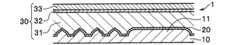
第1実施形態に係る発光素子は、一例として窒化物半導体素子の構成として、図1〜図7を参照しながら説明する。発光素子1は、サファイア基板10と、バッファ層20と、窒化物半導体層30とが積層された構造を備えている。
<First Embodiment>
[Configuration of Light Emitting Element]
The light emitting device according to the first embodiment will be described with reference to FIGS. 1 to 7 as a configuration of a nitride semiconductor device as an example. The light emitting element 1 has a structure in which asapphire substrate 10, abuffer layer 20, and anitride semiconductor layer 30 are stacked.

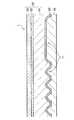
図1及び図3に示すように、サファイア基板10は、窒化物半導体層30を支持するとともに窒化物半導体(例えばGaN)を成長させるためのものである。サファイア基板10は、その主面側となるc面側の上面に平面視で長尺形状の凸部11が複数形成されている。また、サファイア基板10は、前記した凸部11(第1凸部11A、第2凸部11B、第3凸部11C)を含めて、全体として例えば50μm〜300μmの範囲の厚さを有している。なお、第1凸部11A〜第3凸部11Cは、まとめて説明する場合は凸部11として説明する。  As shown in FIGS. 1 and 3, thesapphire substrate 10 supports thenitride semiconductor layer 30 and grows a nitride semiconductor (for example, GaN). Thesapphire substrate 10 is formed with a plurality of longconvex portions 11 in plan view on the upper surface on the c-plane side that is the main surface side. Thesapphire substrate 10 has a thickness in the range of, for example, 50 μm to 300 μm as a whole, including the above-described convex portions 11 (thefirst convex portion 11A, thesecond convex portion 11B, and thethird convex portion 11C). Yes. In addition, the1st convex part 11A-3rd convex part 11C are demonstrated as theconvex part 11, when it demonstrates collectively.

凸部11は、サファイア基板10上に窒化物半導体を結晶成長させる際に、平坦性を改善させる結果、転位密度を低減させると共に結晶配向の良い窒化物半導体層30を形成することができるものである。ここで、図2A及び図2Bに示すように、サファイア基板10は、六方晶の結晶構造を有するサファイア結晶SCで構成されており、c面((0001)面)を主面としている。なお、本明細書におけるc面とは、c面に対してやや傾斜したオフ角が付されたものであってもよい。オフ角の角度は例えば3°以下程度である。前記した凸部11は、この主面であるc面側の表面に形成されている。また、サファイア結晶SCは、c面の他にも、ユニットセル図における六角柱の側面である6つのm面と、a軸、a軸、a軸にそれぞれ直交する3つのa面、すなわち、第1のa面、第2のa面、第3のa面を有している。さらに、m面に直交する方向がm軸方向であり、m軸方向は、a軸、a軸、a軸とそれぞれ30度異なる方向に延びる3つの方向がある。また、m軸は、それぞれ第1のa面〜第3のa面に平行となるように位置しており、ここでは、それぞれ、第1のm軸Sa1、第2のm軸Sa2、第3のm軸Sa3として説明する。Theconvex portion 11 is capable of forming anitride semiconductor layer 30 having a good crystal orientation while reducing dislocation density as a result of improving flatness when a nitride semiconductor is grown on thesapphire substrate 10. is there. Here, as shown in FIGS. 2A and 2B, thesapphire substrate 10 is composed of a sapphire crystal SC having a hexagonal crystal structure, and has a c-plane ((0001) plane) as a main surface. Note that the c-plane in the present specification may have an off angle slightly inclined with respect to the c-plane. The off angle is, for example, about 3 ° or less. The above-mentionedconvex part 11 is formed on the surface on the c-plane side which is this main surface. In addition to the c-plane, the sapphire crystal SC has six m-planes, which are side surfaces of the hexagonal column in the unit cell diagram, and three a-planes orthogonal to the a1 axis, a2 axis, and a3 axis, That is, it has a first a-plane, a second a-plane, and a third a-plane. Furthermore, the direction orthogonal to the m-plane is the m-axis direction, and the m-axis direction includesthree directions extending in directions different from the a1 axis, the a2 axis, and the a3 axis by 30 degrees. Further, the m-axis is positioned so as to be parallel to the first a-plane to the third a-plane, respectively, and here, the first m-axis Sa1, the second m-axis Sa2, the third a-plane, respectively. The m-axis Sa3 will be described.

図3及び図4Aに示すように、凸部11は、それぞれ同一形状で第1のm軸Sa1、第2のm軸Sa2及び第3のm軸Sa3に沿って所定数(例えば、3〜5本:図3では4本)が所定間隔で平行に配列するように形成されている。凸部11(第1凸部11A〜第3凸部11C)は、例えば、その間隔(最短距離)が、長手方向及び短手方向ともに0.3μm〜4μmの範囲内とすることが好ましい。また、凸部11の長手方向の長さ(コア全長L1)及び短手方向の長さ(コア径Da)は、例えば、それぞれ5μm〜25μm及び1μm〜5μmの範囲内とすることが好ましい。そして、凸部11の高さは、例えば0.5μm〜2.5μmの範囲内とすることが好ましい。
また、凸部11は、平面視で長尺形状の長手方向の長さ(各m軸Sa1〜Sa3のそれぞれに平行な方向の長さ)が短手方向の長さ(各m軸Sa1〜Sa3のそれぞれに垂直な方向の長さ)の3倍以上であることが好ましい(6倍〜15倍、あるいは、5倍〜12倍であることが更に好ましい)。そして、凸部11は、長手方向の両端のそれぞれが略同一形状に形成されており、ここでは、平面視でそれぞれ直線状の端部に半円形状に形成されている。なお、凸部11の長手方向における直線部分をコア長さL2とし、凸部11の一端から他端までをコア全長L1とする。そして、ここでは、凸部11は、一例として、コア長さL2と、コア全長L1との比を1対1.05〜1.6の範囲としている。
凸部11は、それぞれのm軸Sa1〜Sa3に平行な直線部分を辺11a〜11cとして外縁にそれぞれ有している。例えば、第1凸部11Aは、平面視において、第1のm軸Sa1に平行な直線状の辺11aを対向して有し、その辺11aの両端部に円弧状の外縁となるような形状に形成されている。そして、第1凸部11Aは、第2凸部11B及び第3凸部11Cの延伸方向に対して60度をなす角度に形成されている。なお、第2凸部11B及び第3凸部11Cについても同様の構成を備えることとなり、詳細は後記する。
As shown in FIGS. 3 and 4A, theconvex portions 11 have the same shape and a predetermined number (for example, 3 to 5) along the first m-axis Sa1, the second m-axis Sa2, and the third m-axis Sa3. (4 in FIG. 3) are arranged in parallel at a predetermined interval. It is preferable that the convex part 11 (1stconvex part 11A-3rdconvex part 11C) makes the space | interval (shortest distance) into the range of 0.3 micrometer-4 micrometers in a longitudinal direction and a transversal direction, for example. Moreover, it is preferable that the length (core total length L1) of theconvex part 11 and the length (core diameter Da) of a transversal direction are the range of 5 micrometers-25 micrometers and 1 micrometer-5 micrometers, respectively, for example. And it is preferable that the height of theconvex part 11 shall be in the range of 0.5 micrometer-2.5 micrometers, for example.
In addition, theconvex portion 11 has a long length in the plan view (length in a direction parallel to each of the m-axis Sa1 to Sa3) and a length in the short direction (each m-axis Sa1 to Sa3). (Length in the direction perpendicular to each) is preferably at least 3 times (6 to 15 times, or more preferably 5 to 12 times). Theconvex portions 11 are formed in substantially the same shape at both ends in the longitudinal direction. Here, theconvex portions 11 are each formed in a semicircular shape at a linear end portion in plan view. In addition, let the linear part in the longitudinal direction of theconvex part 11 be the core length L2, and let the core full length L1 from the one end of theconvex part 11 to the other end. Here, as an example, theconvex portion 11 has a ratio of the core length L2 and the core total length L1 in a range of 1: 1 to 0.05 to 1.6.
Theconvex part 11 has the linear part parallel to each m-axis Sa1-Sa3 as anedge 11a-11c in an outer edge, respectively. For example, the firstconvex portion 11A has alinear side 11a that is parallel to the first m-axis Sa1 in plan view, and has a shape that forms arcuate outer edges at both ends of theside 11a. Is formed. The firstconvex portion 11A is formed at an angle of 60 degrees with respect to the extending direction of the secondconvex portion 11B and the thirdconvex portion 11C. The secondconvex portion 11B and the thirdconvex portion 11C have the same configuration, and details will be described later.

また、図5A〜図5Cに示すように、凸部11は、短手方向(各m軸Sa1〜Sa3のそれぞれに垂直な方向)における断面の上部が平面ではなく尖っている形状を呈している。つまり、凸部11は、短手方向の断面形状において、高さの所定位置から頂部に向かって三角形頂部となるように形成されている。これは、サファイア基板10の上面に垂直な軸であるc軸に対して傾斜した側面を有するドーム形状の凸部11が形成されていることを示している。
さらに、凸部11の全体の個数は、サファイア基板10の面積に応じて、前記した凸部11のそれぞれの間隔及び長さを考慮して決定される。例えば、凸部11は、サファイア基板10の全面にわたって均等に配置されている。
Further, as shown in FIGS. 5A to 5C, theconvex portion 11 has a shape in which the upper part of the cross section in the short direction (direction perpendicular to each of the m-axis Sa1 to Sa3) is not flat but sharp. . That is, theconvex part 11 is formed so that it may become a triangle top part from the predetermined position of height to the top part in the cross-sectional shape of a transversal direction. This indicates that a dome-shapedconvex portion 11 having a side surface inclined with respect to the c-axis that is an axis perpendicular to the upper surface of thesapphire substrate 10 is formed.
Furthermore, the total number of theconvex portions 11 is determined in consideration of the interval and length of each of theconvex portions 11 according to the area of thesapphire substrate 10. For example, theconvex portions 11 are arranged uniformly over the entire surface of thesapphire substrate 10.

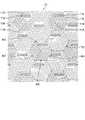
図3及び図4Aに示すように、第1実施形態では、凸部11として、第1のm軸Sa1に沿って配置した第1凸部11Aと、第2のm軸Sa2に沿って配置した第2凸部11Bと、第3のm軸Sa3に沿って配置した第3凸部11Cとを備えている。ここでは、第1凸部11Aの集まり(第1凸部群)を第1サブユニットSU1とし、第2凸部11Bの集まり(第2凸部群)を第2サブユニットSU2とし、第3凸部11Cの集まり(第3凸部群)を第3サブユニットSU3としている。  As shown in FIGS. 3 and 4A, in the first embodiment, as theconvex portion 11, the firstconvex portion 11A disposed along the first m-axis Sa1 and the second m-axis Sa2 are disposed. A secondconvex portion 11B and a thirdconvex portion 11C arranged along the third m-axis Sa3 are provided. Here, a group offirst protrusions 11A (first protrusion group) is a first subunit SU1, a group ofsecond protrusions 11B (second protrusion group) is a second subunit SU2, and a third protrusion A group ofthird portions 11C (third convex portion group) is defined as a third subunit SU3.

さらに、第1凸部11Aは、仮想的な正六角形を三等分する仮想的な菱形の区域となる第1領域Ar1に配置され、第2凸部11Bは、前記した菱形の他の区域となる第2領域Ar2に配置され、第3凸部11Cは、前記した菱形の他の区域となる第3領域Ar3に配置されている。そして、第1凸部11Aが形成された第1領域Ar1と、第2凸部11Bが形成された第2領域Ar2と、第3凸部11Cが形成された第3領域Ar3とを合せた仮想的な六角形を形成する領域を第1ユニットKUとしている。つまり、第1ユニットKUを三等分する各領域が第1領域Ar1〜第3領域Ar3となる。また、第1凸部11A〜第3凸部11Cのそれぞれは、第1ユニットKUにおいて、三回転対称となるように配置されている。  Furthermore, 11 A of 1st convex parts are arrange | positioned in 1st area | region Ar1 used as the area of the virtual rhombus which divides a virtual regular hexagon into three equal parts, and the 2ndconvex part 11B is the other area of the rhombus mentioned above. The 3rdconvex part 11C is arranged in the 3rd field Ar3 used as the other area of the above-mentioned rhombus. Then, the first region Ar1 where the firstconvex portion 11A is formed, the second region Ar2 where the secondconvex portion 11B is formed, and the third region Ar3 where the thirdconvex portion 11C is formed are combined. A region forming a typical hexagon is defined as a first unit KU. That is, each region that divides the first unit KU into three equal parts is the first region Ar1 to the third region Ar3. Moreover, each of the 1stconvex part 11A-the 3rdconvex part 11C is arrange | positioned so that it may become three-fold symmetry in the 1st unit KU.

なお、第1領域Ar1は、第1のm軸Sa1及び第2のm軸Sa2に平行な辺を有する正六角形の第1ユニットKUにおける菱形の領域として、ここでは設定されている。また、第2領域Ar2は、第2のm軸Sa2及び第3のm軸Sa3に平行な辺を有する正六角形の第1ユニットKUにおける菱形の領域として、ここでは設定されている。さらに、第3領域Ar3は、第1のm軸Sa1及び第3のm軸Sa3に平行な辺を有する正六角形の第1ユニットKUにおける菱形の領域として、ここでは設定されている。  The first region Ar1 is set here as a rhombus region in the regular hexagonal first unit KU having sides parallel to the first m-axis Sa1 and the second m-axis Sa2. The second region Ar2 is set here as a rhombic region in the regular hexagonal first unit KU having sides parallel to the second m-axis Sa2 and the third m-axis Sa3. Further, the third region Ar3 is set here as a rhombic region in the regular hexagonal first unit KU having sides parallel to the first m-axis Sa1 and the third m-axis Sa3.

さらに、図3及び図4Bに示すように、サファイア基板10では、第1ユニットKUと、この第1ユニットKUの鏡面対称となる第2ユニットTUとによりユニットパターンを形成するように構成されている。このユニットパターンは、仮想的な正六角形とする第1ユニットKUの第1領域Ar1、第2領域Ar2及び第3領域Ar3の配置が、鏡面対称となり仮想的な正六角形とする第2ユニットTUとの組み合わせにより形成されている。そして、ここでは、第1ユニットKUと第2ユニットTUの組み合わせとして、第1ユニットKUの仮想的な正六角形の各辺に、第2ユニットTUの仮想的な正六角形の1つの辺を合せて配置されるようにユニットパターンが形成されている。  Further, as shown in FIGS. 3 and 4B, thesapphire substrate 10 is configured to form a unit pattern by the first unit KU and the second unit TU that is mirror-symmetrical to the first unit KU. . The unit pattern includes a second unit TU in which the arrangement of the first region Ar1, the second region Ar2, and the third region Ar3 of the first unit KU that is a virtual regular hexagon is mirror-symmetrical and a virtual regular hexagon. It is formed by the combination of. And here, as a combination of the first unit KU and the second unit TU, one side of the virtual regular hexagon of the second unit TU is aligned with each side of the virtual regular hexagon of the first unit KU. Unit patterns are formed so as to be arranged.

なお、第1ユニットKU及び第2ユニットTUとして仮想的に区画される正六角形は、第1凸部11A〜第3凸部11Cを配置するときの仮想的な基準線であり、実際の基板には形成されることはない。また、第1領域Ar1〜第3領域Ar3、あるいは、第1サブユニットSU1〜第3サブユニットSU3として仮想的に区画される菱形は、仮想的な基準線であり、実際の基板には形成されることはない。  Note that the regular hexagons virtually divided as the first unit KU and the second unit TU are virtual reference lines when the firstconvex portion 11A to the thirdconvex portion 11C are arranged, and are formed on the actual substrate. Will not be formed. The rhombus virtually divided as the first region Ar1 to the third region Ar3 or the first subunit SU1 to the third subunit SU3 is a virtual reference line and is formed on an actual substrate. Never happen.

また、第1ユニットKUと第2ユニットTUとが鏡面(鏡像)対称である関係とは、図4Bに示すように、対称軸MGを挟んで一方側に仮想的な正六角形の第1ユニットKUが位置したときの第1領域Ar1〜第3領域Ar3の配置が、対称軸MGの他側に鏡像として写されたときに鏡面対称の位置となる第1領域Ar1〜第3領域Ar3の配置となる仮想的な正六角形の第2ユニットTUである関係をいう。そして、頂角を起点にした第2ユニットTUを平行移動させて第1ユニットKUの各辺に合せるように配置している。例えば、図3に示すように、第1ユニットKUの辺Ha1に第2ユニットTUの辺Hb6を合せ、同様に、辺Ha2に辺Hb5に合せ、辺Ha3に辺Hb4に合せ、辺Ha4に辺Hb3に合せ、辺Ha5に辺Hb2、辺Ha6に辺Hb1を合せるようにしている。  Further, the relationship in which the first unit KU and the second unit TU are mirror-surface (mirror image) symmetrical is, as shown in FIG. 4B, a virtual regular hexagonal first unit KU on one side across the symmetry axis MG. The arrangement of the first area Ar1 to the third area Ar3 when the first area Ar1 to the third area Ar3 are mirror-symmetrical when the arrangement of the first area Ar1 to the third area Ar3 is mirrored on the other side of the symmetry axis MG. The relationship is a virtual regular hexagonal second unit TU. And it arrange | positions so that the 2nd unit TU which made the vertex angle the starting point may be moved in parallel, and it may match with each edge | side of the 1st unit KU. For example, as shown in FIG. 3, the side Hb6 of the second unit TU is aligned with the side Ha1 of the first unit KU, similarly, the side Ha2 is aligned with the side Hb5, the side Ha3 is aligned with the side Hb4, and the side Ha4 is aligned with the side Ha4. According to Hb3, side Hb2 is aligned with side Ha5, and side Hb1 is aligned with side Ha6.

ここでは、第1ユニットKUの頂角が起点となって鏡面対称とし、平行に移動させることで各辺に合せるようにしているが、第1ユニットKUの一辺を対称軸MGに平行にした状態での鏡面対称となる第2ユニットTUでも同様である。つまり、第2ユニットTUは、第1ユニットKUの第1領域Ar1〜第3領域Ar3の配置の関係が鏡面対称となっていればよい。なお、第1ユニットKUの一辺を対称軸MGに平行にした場合の第2ユニットTUは、30度角度を変更して平行移動することで、前記したように、第1ユニットUKの各辺Ha1〜Ha6に、辺Hb1〜Hb6を合せてユニットパターンを形成することになる。また、図4Bに示すように、第2ユニットTUでは、第1凸部11Aは、鏡面対称としているので、傾斜方向が図面上では、第2のm軸に沿った傾斜角度となっている。さらに、第2ユニットTUでは、第2凸部11Bは、鏡面対称となっているので、傾斜方向が図面上では、第1のm軸に沿った傾斜角度となっている。
言い換えると、第2ユニットTUは、第1ユニットKUの正六角形領域を構成する1辺の垂直二等分線に平行をなす直線を基準としたときに、第1ユニットKUと鏡面対称の関係にある(基準となる直線に対して180度回転させた凸部11の配置)。さらに、第2ユニットTUは、1つの第1ユニットKUの正六角形領域を構成する6つの辺Ha1〜Ha6それぞれと、6つの第2ユニットTUの正六角形領域それぞれを構成する辺Hb1〜Hb6のうちの1辺と一致するように、1つの第1ユニットKUに対して6つが配置される。
また、図4Bに示すように、第2ユニットTUでは、第1凸部11Aは、鏡面対称としているので、傾斜方向が図面上では、第2のm軸に沿った傾斜角度となっている。さらに、第2ユニットTUでは、第2凸部11Bは、鏡面対称となっているので、傾斜方向が図面上では、第1のm軸に沿った傾斜角度となっている。
Here, the vertex angle of the first unit KU is the starting point to make it mirror-symmetrical, and it is made to match each side by moving in parallel, but one side of the first unit KU is parallel to the symmetry axis MG. The same applies to the second unit TU that is mirror-symmetrical. That is, in the second unit TU, it is only necessary that the arrangement relationship of the first region Ar1 to the third region Ar3 of the first unit KU is mirror-symmetric. Note that the second unit TU in the case where one side of the first unit KU is parallel to the symmetry axis MG is translated by changing the angle by 30 degrees, and as described above, each side Ha1 of the first unit UK. A unit pattern is formed by aligning the sides Hb1 to Hb6 with .about.Ha6. Further, as shown in FIG. 4B, in the second unit TU, the firstconvex portion 11A is mirror-symmetrical, so that the inclination direction is an inclination angle along the second m-axis in the drawing. Further, in the second unit TU, since the secondconvex portion 11B is mirror-symmetrical, the inclination direction is an inclination angle along the first m-axis in the drawing.
In other words, the second unit TU has a mirror-symmetrical relationship with the first unit KU when a straight line parallel to the vertical bisector of one side constituting the regular hexagonal region of the first unit KU is used as a reference. There is (arrangement of theconvex portions 11 rotated 180 degrees with respect to the reference straight line). Further, the second unit TU includes six sides Ha1 to Ha6 that constitute a regular hexagonal region of one first unit KU and sides Hb1 to Hb6 that constitute a regular hexagonal region of six second units TU. Six are arranged with respect to one first unit KU so as to coincide with one side.
Further, as shown in FIG. 4B, in the second unit TU, the firstconvex portion 11A is mirror-symmetrical, so that the inclination direction is an inclination angle along the second m-axis in the drawing. Further, in the second unit TU, since the secondconvex portion 11B is mirror-symmetrical, the inclination direction is an inclination angle along the first m-axis in the drawing.

図3及び図4Aに示すように、複数の第1凸部11Aは、第1のm軸Sa1に沿ってそれぞれが形成され、同じ形状となるように構成されている。第1ユニットKUの第1凸部11Aは、仮想的に形成した正六角形を三等分する菱形の第1領域Ar1内において、第1のm軸Sa1に沿って延伸させて長尺形状に形成して配置されている。そして、第1凸部11Aは、4本のそれぞれの一端部及び他端部が第2のm軸Sa2に沿って揃うように等間隔で並列して配置されている。
つまり、複数の第1凸部11Aは、第1領域Ar1となる菱形領域の一対の対辺に平行に延伸すると共に他の一対の対辺に沿って等間隔に配置されている。そして、第1領域Ar1内に配置された複数の第1凸部11Aは、その延伸方向が、隣接する他の2つの菱形領域となる第2領域Ar2及び第3領域Ar3に設けられた凸部11B,11Cの延伸方向と60度をなすように配置されている。
第1凸部11Aは、4本の集合を第1サブユニットSU1として、第1領域Ar1に第1間隔da1を空けると共に、第4間隔ds1を空けて配置されている。第1サブユニットSU1では、第1凸部11Aが、その一側の端部を正六角形状の一辺に接するように揃え、その他側の端部を第2領域Ar2側から所定間隔となる第1間隔da1を空けて同一の第2のm軸Sa2に揃うように配置されている。なお、第4間隔ds1は、第1領域Ar1において、仮想的な正六角形の中心点側から一番遠くに位置する第1凸部11Aと、前記正六角形の一辺との間の間隔であり、ここでは、第1凸部11A同士間の間隔と略同等となるように設定されている。
As shown in FIGS. 3 and 4A, the plurality of firstconvex portions 11A are formed along the first m-axis Sa1 so as to have the same shape. The firstconvex portion 11A of the first unit KU is formed in a long shape by extending along the first m-axis Sa1 in the rhombic first region Ar1 that divides the virtually formed regular hexagon into three equal parts. Are arranged. The firstconvex portions 11A are arranged in parallel at equal intervals so that the respective one end portions and the other end portions of the four protrusions are aligned along the second m-axis Sa2.
That is, the plurality offirst protrusions 11A extend in parallel to a pair of opposite sides of the rhombic region that becomes the first region Ar1, and are arranged at equal intervals along the other pair of opposite sides. The plurality of firstconvex portions 11A arranged in the first region Ar1 are convex portions provided in the second region Ar2 and the third region Ar3 whose extending directions are the other two adjacent rhombic regions. It arrange | positions so that the extending | stretching direction of 11B and 11C may make 60 degree | times.
The firstconvex portion 11A is arranged with four sets as the first subunit SU1, with a first interval da1 and a fourth interval ds1 in the first region Ar1. In the first subunit SU1, the firstconvex portion 11A is arranged so that one end thereof is in contact with one side of the regular hexagon, and the other end is set at a predetermined interval from the second region Ar2 side. They are arranged so as to be aligned with the same second m-axis Sa2 with an interval da1. The fourth interval ds1 is the interval between the firstconvex portion 11A located farthest from the center point side of the virtual regular hexagon in the first region Ar1 and one side of the regular hexagon. Here, it is set to be substantially equal to the interval between the firstconvex portions 11A.

したがって、図4Aに示すように、第1凸部11Aの他側の端部から第2領域Ar2までの間となる第1間隔da1は、第1凸部11Aが4本とも均等となるように構成されている。そして、第2のm軸Sa2に沿って第1間隔da1の略範囲のままで連続することができる領域は、第3領域Ar3において正六角形の中心に最も近い第3凸部11Cを越えて当該中心に2番目に近い第3凸部11Cに到達するまで形成されている。特に、第1領域Ar1において正六角形の中心に最も近い第1凸部11Aの位置が、当該中心に最も近い第2凸部11Bの端部から、第3のm軸Sa3に平行で第1領域Ar1に向かう接線Ya2に交わらないように離間して配置されている。そのため、ユニット中央において、第2のm軸Sa2に沿って連続する領域は、第1間隔da1の間隔のまま第1領域Ar1から第3領域Ar3に亘って形成することができる。なお、接線Ya2は、第2凸部11Bの端部に接する第3のm軸Sa3と平行をなす仮想的な線である。  Therefore, as shown in FIG. 4A, the first interval da1 between the other end of thefirst protrusion 11A and the second region Ar2 is such that all fourfirst protrusions 11A are equal. It is configured. Then, the region that can continue in the approximate range of the first interval da1 along the second m-axis Sa2 exceeds the thirdconvex portion 11C closest to the center of the regular hexagon in the third region Ar3. It is formed until it reaches the thirdconvex portion 11C that is second closest to the center. In particular, the position of the firstconvex portion 11A closest to the center of the regular hexagon in the first region Ar1 is parallel to the third m-axis Sa3 from the end of the secondconvex portion 11B closest to the center. They are spaced apart so as not to intersect the tangent line Ya2 toward Ar1. Therefore, in the center of the unit, a region continuous along the second m-axis Sa2 can be formed from the first region Ar1 to the third region Ar3 while maintaining the interval of the first interval da1. The tangent line Ya2 is a virtual line that is parallel to the third m-axis Sa3 that is in contact with the end of the secondconvex portion 11B.

また、第1ユニットKUの第2凸部11Bは、仮想的に形成した正六角形を三等分する菱形の第2領域Ar2内において、第2のm軸Sa2に沿って延伸させて長尺形状に形成して配置されている。そして、第2凸部11Bは、4本のそれぞれの一端部及び他端部が第3のm軸Sa3に沿って揃うように等間隔で並列して配置されている。
つまり、複数の第2凸部11Bは、第2領域Ar2となる菱形領域の一対の対辺に平行に延伸すると共に他の一対の対辺に沿って等間隔に配置されている。そして、第2領域Ar2内に配置された複数の第2凸部11Bは、その延伸方向が、隣接する他の2つの菱形領域となる第1領域Ar1及び第3領域Ar3に設けられた凸部11A,11Cの延伸方向と60度をなすように配置されている。
第2凸部11Bは、4本の集合を第2サブユニットSU2として、第2領域Ar2に第2間隔da2を空けると共に、第5間隔ds2を空けて配置されている。第2サブユニットSU2では、第2凸部11Bが、その一側の端部を正六角形状の一辺に接するように揃え、その他側の端部を第3領域Ar3側から所定間隔を空けて同一の第3のm軸Sa3に揃うように配置されている。なお、第5間隔ds2は、第2領域Ar2において、仮想的な正六角形の中心点側から一番遠くに位置する第2凸部11Bと、前記正六角形の一辺との間の間隔であり、ここでは、第2凸部11B同士間の間隔と略同等となるように設定されている。
Further, the secondconvex portion 11B of the first unit KU is elongated by extending along the second m-axis Sa2 in the rhombic second region Ar2 that divides the virtually formed regular hexagon into three equal parts. It is formed and arranged. And the 2ndconvex part 11B is arrange | positioned in parallel at equal intervals so that each one end part and other end part of four may align along 3rd m-axis Sa3.
That is, the plurality of secondconvex portions 11B extend in parallel to the pair of opposite sides of the rhombic region that becomes the second region Ar2, and are arranged at equal intervals along the other pair of opposite sides. And the 2ndconvex part 11B arrange | positioned in 2nd area | region Ar2 is the convex part provided in 1st area | region Ar1 and 3rd area | region Ar3 whose extension direction becomes other two adjacent rhombus area | regions It arrange | positions so that the extending | stretching direction of 11A and 11C may make 60 degree | times.
The secondconvex portion 11B is arranged with a set of four as the second subunit SU2, with a second interval da2 and a fifth interval ds2 in the second region Ar2. In the second subunit SU2, the secondconvex portion 11B is aligned so that one end thereof is in contact with one side of the regular hexagon, and the other end is the same with a predetermined interval from the third region Ar3 side. Are arranged so as to be aligned with the third m-axis Sa3. The fifth interval ds2 is the interval between the secondconvex portion 11B located farthest from the center point side of the virtual regular hexagon and the one side of the regular hexagon in the second region Ar2. Here, it is set to be substantially equal to the interval between the secondconvex portions 11B.

したがって、図4Aに示すように、第2凸部11Bの他側の端部から第3領域Ar3までの間となる第2間隔da2は、第2凸部11Bが4本とも均等となるように構成されている。そして、第3のm軸Sa3に沿って第2間隔da2の略範囲のままで連続することができる領域は、第2領域Ar2において正六角形の中心に最も近い第1凸部11Aを越えて当該中心に2番目に近い第1凸部11Aに到達するまで形成されている。特に、第2領域Ar2において正六角形の中心に最も近い第2凸部11Bの位置が、当該中心に最も近い第3凸部11Cの端部から、第1のm軸Sa1に平行で第2領域Ar2に向かう接線Ya3に交わらないように離間して配置されている。そのため、ユニット中央において、第3のm軸Sa3に沿って連続する領域は、第2間隔da2の間隔のまま第2領域Ar2から第1領域Ar1に亘って形成することができる。なお、接線Ya3は、第3凸部11Cの端部に接する第1のm軸Sa1と平行をなす仮想的な線である。  Therefore, as shown in FIG. 4A, the second interval da2 between the other end of the secondconvex portion 11B and the third region Ar3 is such that all the four secondconvex portions 11B are equal. It is configured. Then, the region that can continue in the approximate range of the second interval da2 along the third m-axis Sa3 exceeds the firstconvex portion 11A closest to the center of the regular hexagon in the second region Ar2. It is formed until it reaches the firstconvex portion 11A that is second closest to the center. In particular, the position of the secondconvex portion 11B closest to the center of the regular hexagon in the second region Ar2 is parallel to the first m-axis Sa1 from the end of the thirdconvex portion 11C closest to the center. They are spaced apart so as not to intersect the tangent line Ya3 toward Ar2. For this reason, in the center of the unit, a region continuous along the third m-axis Sa3 can be formed from the second region Ar2 to the first region Ar1 with the interval of the second interval da2. The tangent line Ya3 is a virtual line that is parallel to the first m-axis Sa1 that is in contact with the end of the thirdconvex portion 11C.

さらに、第1ユニットKUの第3凸部11Cは、仮想的に形成した正六角形を三等分する菱形の第3領域Ar3内において、第3のm軸Sa3に沿って延伸させて長尺形状に形成して配置されている。そして、第3凸部11Cは、4本のそれぞれの一端部及び他端部が第1のm軸Sa1に沿って揃うように等間隔で並列して配置されている。
つまり、複数の第3凸部11Cは、第3領域Ar3となる菱形領域の一対の対辺に平行に延伸すると共に他の一対の対辺に沿って等間隔に配置されている。そして、第3領域Ar3内に配置された第3凸部11Cは、その延伸方向が、隣接する他の2つの菱形領域となる第1領域Ar1及び第2領域Ar2に設けられた凸部11A,11Bの延伸方向と60度をなすように配置されている。
第3凸部11Cは、4本の集合を第3サブユニットSU3として、第3領域Ar3に第3間隔da3を空けると共に、第6間隔ds3を空けて配置されている。第3サブユニットSU3では、第3凸部11Cが、その一側の端部を正六角形状の一辺に接するように揃え、その他側の端部を第1領域Ar1側から所定間隔を空けて同一の第1のm軸Sa1に揃うように配置されている。なお、第6間隔ds3は、第3領域Ar3において、仮想的な正六角形の中心点側から一番遠くに位置する第3凸部11Cと、前記正六角形の一辺との間の間隔であり、ここでは、第3凸部11C同士間の間隔と略同等となるように構成されている。
Furthermore, the 3rdconvex part 11C of 1st unit KU is extended | stretched along the 3rd m-axis Sa3 in 3rd rhombus 3rd area | region Ar3 which divides the regular hexagon formed virtually into three equal parts. It is formed and arranged. Thethird protrusions 11C are arranged in parallel at equal intervals so that the one end and the other end of each of the four are aligned along the first m-axis Sa1.
That is, the plurality of thirdconvex portions 11C extend in parallel to a pair of opposite sides of the rhombic region that becomes the third region Ar3 and are arranged at equal intervals along the other pair of opposite sides. And the 3rdconvex part 11C arrange | positioned in 3rd area | region Ar3 is 11 A of convex parts provided in 1st area | region Ar1 and 2nd area | region Ar2 from which the extending | stretching direction becomes two adjacent rhombus area | regions. It arrange | positions so that the extending | stretching direction of 11B may make 60 degree | times.
The thirdconvex portion 11C is arranged with a set of four as the third subunit SU3, with a third interval da3 and a sixth interval ds3 in the third region Ar3. In the third subunit SU3, thethird protrusion 11C is aligned so that one end thereof is in contact with one side of the regular hexagon, and the other end is the same at a predetermined interval from the first region Ar1 side. Are arranged so as to be aligned with the first m-axis Sa1. Note that the sixth interval ds3 is an interval between the thirdconvex portion 11C located farthest from the center point side of the virtual regular hexagon in the third region Ar3 and one side of the regular hexagon. Here, it is comprised so that it may become substantially equivalent to the space | interval between the 3rdconvex parts 11C.

したがって、図4Aに示すように、第3凸部11Cの他側の端部から第1領域Ar1までの間となる第3間隔da3は、4本とも均等となるように構成されている。そして、第1のm軸Sa1に沿って第3間隔da3の略範囲のままで連続することができる領域は、第2領域Ar2において正六角形の中心に最も近い第2凸部11Bを越えて当該中心に2番目に近い第2凸部11Bに到達するまで形成されている。特に、第3領域Ar3において正六角形の中心に最も近い第3凸部11Cの位置が、当該中心に最も近い第1凸部11Aの端部から、第2のm軸Sa2に平行で第3領域Ar3に向かう接線Ya1に交わらないように離間して配置されている。そのため、ユニット中央において、第1のm軸Sa1に沿って連続する領域は、第3間隔da3の間隔のまま第3領域Ar3から第2領域Ar2に亘って形成することができる。なお、接線Ya1は、第1凸部11Aの端部に接する第2のm軸Sa2と平行をなす仮想的な線である。  Therefore, as shown to FIG. 4A, the 3rd space | interval da3 from the other edge part of the 3rdconvex part 11C to 1st area | region Ar1 is comprised so that all four may become equal. Then, the region that can continue in the approximate range of the third interval da3 along the first m-axis Sa1 exceeds the secondconvex portion 11B closest to the center of the regular hexagon in the second region Ar2. It is formed until it reaches the secondconvex portion 11B that is second closest to the center. In particular, the position of the thirdconvex portion 11C closest to the center of the regular hexagon in the third region Ar3 is parallel to the second m-axis Sa2 from the end of the firstconvex portion 11A closest to the center. They are spaced apart so as not to intersect the tangent line Ya1 that faces Ar3. For this reason, in the center of the unit, a region continuous along the first m-axis Sa1 can be formed from the third region Ar3 to the second region Ar2 with the interval of the third interval da3. The tangent line Ya1 is a virtual line that is parallel to the second m-axis Sa2 that is in contact with the end of the firstconvex portion 11A.

なお、第1ユニットKU及び第2ユニットTUでは、仮想的な正六角形の中心に最も近い第1凸部11A、第2凸部11B及び第3凸部11Cのうちの少なくとも2つが、対応する接線Ya1、接線Ya2、接線Ya3のいずれかと交わることがないように離間して配置されていればよい。例えば、第1凸部11Aが第1間隔da1を狭くするように接線Ya2に当接するように配置されていても、第2凸部11B及び第3凸部11Cが接線Ya1あるいは接線Ya3から離間して配置されていればよい。第2凸部11B及び第3凸部11Cについても同様である。
つまり、第1ユニットKU及び第2ユニットTUでは、正六角形の中心に最も近い第1凸部11Aは、前記中心に最も近い第2凸部11Bにおける前記中心側の端部に接する第3のm軸Sa3と平行をなす接線Ya2と交わらないように配置されることになる。また、第1ユニットKU及び第2ユニットTUでは、正六角形の中心に最も近い第2凸部11Bは、前記中心に最も近い第3凸部11Cにおける前記中心側の端部に接する第1のm軸Sa1と平行をなす接線Ya3と交わらないように配置されている。
In the first unit KU and the second unit TU, at least two of the firstconvex portion 11A, the secondconvex portion 11B, and the thirdconvex portion 11C that are closest to the center of the virtual regular hexagon are corresponding tangent lines. What is necessary is just to be spaced apart so that it may not cross any of Ya1, tangent line Ya2, and tangent line Ya3. For example, even if the firstconvex portion 11A is disposed so as to contact the tangent line Ya2 so as to narrow the first interval da1, the secondconvex portion 11B and the thirdconvex portion 11C are separated from the tangent line Ya1 or the tangent line Ya3. As long as they are arranged. The same applies to the secondconvex portion 11B and the thirdconvex portion 11C.
That is, in the first unit KU and the second unit TU, the firstconvex portion 11A closest to the center of the regular hexagon is the third m in contact with the center-side end portion of the secondconvex portion 11B closest to the center. It is arranged so as not to intersect the tangent line Ya2 that is parallel to the axis Sa3. Further, in the first unit KU and the second unit TU, the secondconvex portion 11B closest to the center of the regular hexagon is the first m in contact with the end portion on the center side of the thirdconvex portion 11C closest to the center. They are arranged so as not to intersect the tangent line Ya3 that is parallel to the axis Sa1.

また、図6及び図7に示すように、第1ユニットKU及び第2ユニットTUは、第1凸部11Aを、第1領域Ar1に第1間隔da1及び第4間隔ds1を空けて配置させ、第2凸部11Bを、第2領域Ar2に第2間隔da2及び第5間隔ds2を空けて配置させ、さらに、第3凸部11Cを、第3領域Ar3に第3間隔da3及び第6間隔ds3を空けて配置させている。そのため、第1凸部11A〜第3凸部11Cの設置間隔がユニットパターンにおいて互いに略均等となるように配置されることになる。  As shown in FIGS. 6 and 7, the first unit KU and the second unit TU have thefirst protrusion 11A arranged in the first area Ar1 with a first interval da1 and a fourth interval ds1. The secondconvex portion 11B is arranged in the second region Ar2 with the second interval da2 and the fifth interval ds2, and the thirdconvex portion 11C is arranged in the third region Ar3 with the third interval da3 and the sixth interval ds3. It is arranged with a gap. Therefore, the installation intervals of the firstconvex portion 11A to the thirdconvex portion 11C are arranged so as to be substantially equal to each other in the unit pattern.

図7に示すように、第1ユニットKU及び第2ユニットTUは、凸部11同士の間隔において、仮想的な正六角形の中央の領域CE1,CE2及び、仮想的な正六角形の頂角同士の各領域SEにおいても、他の領域との関係で極端に間隔が異なる部分が改善され略均等になるように構成される。
したがって、第1ユニットKU及び第2ユニットTUは、このようなユニットパターンを備えることで、従来の構成と比較して、窒化物半導体、例えば、GaNの結晶成長において成長速度がサファイア基板10の面内で整う(言い換えると、成長過程における窒化物半導体層30の転位密度が低減できる傾向にあると共に、窒化物半導体層30の結晶配光も良くなる)。
As shown in FIG. 7, the first unit KU and the second unit TU have a virtual regular hexagonal central region CE1, CE2 and a virtual regular hexagonal apex angle between theconvex portions 11. Each region SE is also configured so that portions with extremely different intervals in relation to other regions are improved and become substantially equal.
Therefore, the first unit KU and the second unit TU are provided with such a unit pattern, so that the growth rate in the crystal growth of the nitride semiconductor, for example, GaN, is higher than that of the conventional configuration. (In other words, the dislocation density of thenitride semiconductor layer 30 in the growth process tends to be reduced, and the crystal light distribution of thenitride semiconductor layer 30 is improved).

なお、凸部11の配置パターンでは、第1ユニットKU及び第2ユニットTUの対向する頂角部分が6箇所形成されることになる。そして、ユニット同士の対向する6箇所の頂角部分では、前記したサブユニット単位あるいは領域単位であると、仮想的な菱形の頂角を4カ所対向させた部分と、仮想的な菱形の頂角を5カ所対向させた部分とが形成される。また、ユニット中央において、仮想的な菱形の頂角を3つ対向させた部分が形成されることになる(従来の構成は例えば図10A参照:図10Aでは、頂角は6つと3つの2種類のみの配置)。つまり、第1ユニットKU及び第2ユニットTUによるユニットパターンとすることで、仮想的な頂角の位置において、サブユニット単位あるいは領域単位で、頂角の数の異なる部分が設定され、凸部11の間隔を調整しやすい配置にすることができる。  In addition, in the arrangement pattern of theconvex part 11, the apex angle part which the 1st unit KU and the 2nd unit TU oppose is formed in six places. And in the 6 apex portions where the units are opposed to each other, the unit of the subunit or the area unit described above is a portion where the apex angles of the virtual rhombus are opposed to 4 locations, and the apex angle of the virtual rhombus Are formed at five locations facing each other. Further, in the center of the unit, a portion in which three vertices of the virtual rhombus are opposed to each other is formed (see, for example, FIG. 10A for the conventional configuration: in FIG. Only placement). That is, by forming a unit pattern by the first unit KU and the second unit TU, portions having different numbers of apex angles are set in units of subunits or regions at the position of the virtual apex angle, and theconvex portion 11 It is possible to make the arrangement easy to adjust the interval.

また、図5A〜図5Cに示すように、第1凸部11A〜第3凸部11Cは、短手方向における断面の上部が平面ではなく尖っている形状を呈しているため、窒化物半導体の表面に現れる貫通転位の数を減少させることができる。なお、仮に、凸部11の断面形状が図示しない台形状等の上平面のある形状である場合では、その上平面(c面)からも窒化物半導体が成長することになる。そして、この上面から成長する窒化物半導体は横方向にほとんど成長しないため、成長方向に発生した複数の転位が収束せず、窒化物半導体表面の転位密度が増大することになる。一方、前記したように凸部11の断面形状に上平面が存在しない場合、凸部11の上部からの成長が抑制されて窒化物半導体が横方向に成長する。そのため、この凸部11は、成長方向に発生した複数の転位が収束し、転位密度が低減されることになる。  Further, as shown in FIGS. 5A to 5C, the firstconvex portion 11A to the thirdconvex portion 11C have a shape in which the upper part of the cross section in the lateral direction is pointed instead of a flat surface, so that the nitride semiconductor The number of threading dislocations appearing on the surface can be reduced. If the cross-sectional shape of theconvex portion 11 is a shape having an upper plane such as a trapezoidal shape (not shown), the nitride semiconductor grows also from the upper plane (c-plane). Since the nitride semiconductor grown from the upper surface hardly grows in the lateral direction, a plurality of dislocations generated in the growth direction do not converge, and the dislocation density on the nitride semiconductor surface increases. On the other hand, when there is no upper plane in the cross-sectional shape of theconvex portion 11 as described above, the growth from the upper portion of theconvex portion 11 is suppressed and the nitride semiconductor grows in the lateral direction. Therefore, in theconvex portion 11, a plurality of dislocations generated in the growth direction converge and the dislocation density is reduced.

さらに、結晶成長においては比較的安定な結晶面がファセット面として現れる傾向があり、六方晶の窒化物半導体(例えばGaN)は、窒化物半導体のm面からやや傾斜した面をファセット面として結晶成長する。よって、凸部11の長手方向の先端が平面視で半円形状であれば、各ファセット面をほぼ均等な幅で成長させることができ、窒化物半導体を当該半円の中心付近に向かって接合させることができる。窒化物半導体の結晶成長の際に、窒化物半導体がサファイア基板10のc面(凸部11が形成されていない平坦面)から主に成長するため、凸部11上で合わさるように横方向にも均等に成長させることができる(図8A及び図8Bにおいて、転位の詳細な説明は後記する)。  Furthermore, in crystal growth, a relatively stable crystal plane tends to appear as a facet plane, and a hexagonal nitride semiconductor (eg, GaN) grows with a plane slightly inclined from the m plane of the nitride semiconductor as a facet plane. To do. Therefore, if the front end in the longitudinal direction of theconvex portion 11 is a semicircular shape in plan view, each facet surface can be grown with a substantially uniform width, and the nitride semiconductor is bonded toward the vicinity of the center of the semicircle. Can be made. During the crystal growth of the nitride semiconductor, the nitride semiconductor grows mainly from the c-plane of the sapphire substrate 10 (a flat surface on which theconvex portions 11 are not formed). Can be grown evenly (in FIGS. 8A and 8B, a detailed description of dislocations will be given later).

図1に戻って発光素子1の構成について説明を続ける。バッファ層20は、サファイア基板10と当該サファイア基板10上に成長させる窒化物半導体との格子定数差を緩衝させるためのものである。バッファ層20は、サファイア基板10と窒化物半導体層30との間に形成されている。このバッファ層20は例えばAlNやAlGaNで構成される。バッファ層20は、後記するように、製造方法のバッファ層形成工程において、例えば所定条件下でスパッタリングを行うことで形成することができる。バッファ層20は、例えば図1に示すようなサファイア基板10を被覆する層状であるが、一部でサファイア基板10が露出していてもよい。  Returning to FIG. 1, the description of the configuration of the light-emitting element 1 will be continued. Thebuffer layer 20 is for buffering the lattice constant difference between thesapphire substrate 10 and the nitride semiconductor grown on thesapphire substrate 10. Thebuffer layer 20 is formed between thesapphire substrate 10 and thenitride semiconductor layer 30. Thebuffer layer 20 is made of, for example, AlN or AlGaN. As will be described later, thebuffer layer 20 can be formed, for example, by performing sputtering under predetermined conditions in the buffer layer forming step of the manufacturing method. Thebuffer layer 20 is, for example, a layer that covers thesapphire substrate 10 as shown in FIG. 1, but thesapphire substrate 10 may be partially exposed.

窒化物半導体層30は、発光素子1の発光部を構成するものであり、例えば、InAlGa1−X−YN(0≦X,0≦Y,X+Y≦1))等の窒化物半導体が用いられる。窒化物半導体層30は、図1に示すように、サファイア基板10のc面(主面)上にバッファ層20を介して形成されており、n型半導体層31、活性層32及びp型半導体層33が下からこの順に積層された構造を有している。活性層32は、例えば井戸層(発光層)と障壁層とを有する量子井戸構造である。Thenitride semiconductor layer 30 constitutes a light-emitting portion of the light-emitting element 1, for example, nitriding such as InX AlY Ga1- XYN (0 ≦ X, 0 ≦ Y, X + Y ≦ 1)) A physical semiconductor is used. As shown in FIG. 1, thenitride semiconductor layer 30 is formed on the c-plane (main surface) of thesapphire substrate 10 via thebuffer layer 20, and includes an n-type semiconductor layer 31, anactive layer 32, and a p-type semiconductor. Thelayer 33 has a structure in which the layers are stacked in this order from the bottom. Theactive layer 32 has a quantum well structure having, for example, a well layer (light emitting layer) and a barrier layer.

ここで、図8A及び図8Bを参照して、結晶成長と転位についての説明をする。凸部11が形成されていない平坦なサファイア基板10を用いる場合は窒化物半導体が横方向に成長することができないが、前記したようにサファイア基板10上に凸部11が形成されている場合、窒化物半導体の成長時において、窒化物半導体が横方向にも成長することができる。基本的に転位は結晶の成長方向に進行するため、図8A及び図8Bに示すように、窒化物半導体が凸部11上に向かって横方向に成長することで、窒化物半導体中の転位も凸部11上に向かって横方向に進行する。そして、凸部11上において窒化物半導体が接合されることで転位も接合され、閉ループを作る等して最終的な窒化物半導体の表面に転位が現れにくくなる。なお、図8A及び図8Bでは、時間的には図8Bの状態から図8Aの状態に成長するように図示している。  Here, crystal growth and dislocation will be described with reference to FIGS. 8A and 8B. In the case of using aflat sapphire substrate 10 on which theconvex portion 11 is not formed, the nitride semiconductor cannot grow in the lateral direction, but when theconvex portion 11 is formed on thesapphire substrate 10 as described above, During the growth of the nitride semiconductor, the nitride semiconductor can also grow in the lateral direction. Since dislocations basically proceed in the crystal growth direction, as shown in FIGS. 8A and 8B, the nitride semiconductor grows laterally on theconvex portion 11, so that dislocations in the nitride semiconductor also occur. It proceeds in the lateral direction toward theconvex portion 11. Then, dislocations are also joined by joining the nitride semiconductor on theconvex portion 11, and dislocations hardly appear on the surface of the final nitride semiconductor by creating a closed loop. In FIGS. 8A and 8B, the state is shown so as to grow from the state of FIG. 8B to the state of FIG. 8A in terms of time.

このように、窒化物半導体がファセット面を露出した状態を維持しながら徐々に接合されていくことで、転位の数が減少し、窒化物半導体層30の転位密度が低くなる。このとき、図8Bから図8Aの状態として示すように、窒化物半導体がファセット面を露出した状態の時間が長い(ファセット面を露出した状態で成長した膜厚が厚い)方が、転位が収束されやすく、転位の数を減少させやすい。なお、凸部11のユニットパターンを前記したように構成することで、従来に比較して短時間で転位を収束してサファイア基板10から近い位置において平坦な面となるように結晶成長することができる。また、図8A及び図8Bでは、横方向成長中の転位の進行方向が一方向であるが、転位の進行方向は途中で変化することがある。例えば、初期は上方向に進行し、途中から横方向または斜め上方向に進行することがある。  As described above, the nitride semiconductor is gradually joined while maintaining the facet face exposed state, whereby the number of dislocations is reduced and the dislocation density of thenitride semiconductor layer 30 is lowered. At this time, as shown in the states of FIG. 8B to FIG. 8A, dislocations converge when the nitride semiconductor has a longer time in which the facet surface is exposed (thick film grown with the facet surface exposed). It is easy to reduce the number of dislocations. In addition, by constructing the unit pattern of theconvex portion 11 as described above, the dislocations can be converged in a short time compared to the conventional case, and the crystal can be grown so as to be a flat surface at a position near thesapphire substrate 10. it can. Further, in FIGS. 8A and 8B, although the dislocation progress direction during lateral growth is one direction, the dislocation progress direction may change midway. For example, it may progress upward in the initial stage, and may progress laterally or obliquely upward from the middle.

凸部11を、その長手方向に延びる外縁がサファイア基板10の第1のm軸Sa1〜第3のm軸Sa3に沿った角度となる方向に延びる形状とすることで、窒化物半導体が凸部11上で合わさるまで成長速度が整えられ短い時間で平坦面にすることができる。これについて、以下、窒化物半導体の代表的な1つであるGaNを例にして説明する。  By forming theprotrusion 11 in a shape in which the outer edge extending in the longitudinal direction extends in an angle along the first m-axis Sa1 to the third m-axis Sa3 of thesapphire substrate 10, the nitride semiconductor is a protrusion. The growth rate is adjusted until they are combined on 11, and a flat surface can be obtained in a short time. This will be described below using GaN, which is a typical nitride semiconductor, as an example.

六方晶系のGaNは、上方向をc軸方向として結晶成長する。そして、横方向においてはa軸方向よりもm軸方向のほうが成長しにくいため、平面視でGaNのm面(サファイア基板10のc面と垂直に交わる面)に等価な面とサファイア基板10のc面の交線を底辺とするファセット面を維持して成長する傾向がある。このとき、GaNのm面は、サファイア基板10のa面と同一平面に沿って位置している。つまり、GaNは、平面視でサファイア基板10のa面と一致する線を底辺とするファセット面を維持して成長する傾向にある。そこで、サファイア基板10の表面に、サファイア基板10のm面と異なる面(典型的にはa面)に沿って、長手方向に外縁が延びる長尺状の凸部11を配置する。これにより、凸部11の長手方向に延びる外縁がGaNのa面と一致しなくなり、ファセット面の底辺が凸部11の長手方向に延びる外縁と平行になる。  Hexagonal GaN grows with the upper direction as the c-axis direction. In the lateral direction, the m-axis direction is less likely to grow than the a-axis direction. Therefore, a plane equivalent to the m-plane of GaN (a plane perpendicular to the c-plane of the sapphire substrate 10) and thesapphire substrate 10 in plan view. There is a tendency to grow while maintaining the facet plane with the intersection of the c-plane as the base. At this time, the m-plane of GaN is located along the same plane as the a-plane of thesapphire substrate 10. That is, GaN tends to grow while maintaining a facet plane with a line that coincides with the a-plane of thesapphire substrate 10 in plan view. In view of this, on the surface of thesapphire substrate 10, along the surface different from the m-plane of the sapphire substrate 10 (typically the a-plane), an elongatedconvex portion 11 whose outer edge extends in the longitudinal direction is disposed. As a result, the outer edge extending in the longitudinal direction of theconvex portion 11 does not coincide with the a-plane of GaN, and the base of the facet surface is parallel to the outer edge extending in the longitudinal direction of theconvex portion 11.

その結果、凸部11の長手方向に延びる外縁がGaNのa面と一致する場合、つまりファセット面の底辺が凸部11の長手方向に延びる外縁と非平行である場合と比べて、凸部11の短手方向におけるGaNの成長速度が遅くなる。従って、上方向成長よりも凸部11上において横方向成長をする時間が長くなり、転位が収束しやすいので、転位密度を低減することができる。また、窒化物半導体が成長しやすい方向(GaNのa軸方向)が凸部11の短手方向と一致していると、凸部11の短手方向の両側から成長した窒化物半導体が広範囲で接合するため、接合する際に新たな転位が発生するおそれがある。そこで、凸部11の短手方向を、窒化物半導体が成長しやすいGaNのa軸方向からずらして配置する(ここではサファイア基板10の凸部11の長手方向を、サファイア基板10の各m軸に沿って配置する)ことにより、凸部11の長手方向の両側から成長した窒化物半導体が接合することになるため、新たな転位の発生を抑制することができると考えられる。  As a result, when the outer edge extending in the longitudinal direction of theconvex portion 11 coincides with the a-plane of GaN, that is, compared with the case where the bottom of the facet surface is not parallel to the outer edge extending in the longitudinal direction of theconvex portion 11. The growth rate of GaN in the short direction is slow. Therefore, the time for lateral growth on theconvex portion 11 is longer than the upward growth, and the dislocations are likely to converge, so that the dislocation density can be reduced. Further, when the direction in which the nitride semiconductor is likely to grow (a-axis direction of GaN) coincides with the short direction of theconvex portion 11, a wide range of nitride semiconductors grown from both sides of theconvex portion 11 in the short direction. Because of the joining, new dislocations may occur when joining. Therefore, the short direction of theconvex portion 11 is shifted from the a-axis direction of GaN on which the nitride semiconductor is likely to grow (here, the longitudinal direction of theconvex portion 11 of thesapphire substrate 10 is each m-axis of the sapphire substrate 10). , The nitride semiconductor grown from both sides in the longitudinal direction of theconvex portion 11 is joined, so that it is considered that generation of new dislocations can be suppressed.

また、発光素子1は、前記したように窒化物半導体のファセット面が凸部11の長手方向に延びる外縁と一致しているので、先端部付近から徐々に窒化物半導体が成長し、凸部11の中心付近に収束する。そのため、平面視で、凸部11の上方となる位置において、凸部11の長手方向における中央に転位が残る範囲が小さく(狭く)、さらに転位密度も小さくなる傾向にある。一方、例えば、凸部11の長手方向に延びる外縁がサファイア基板10の各m軸に対して±10°の範囲を越える方向である場合(例えば第1のm軸Sa1方向と直交する方向に長手方向が一致する場合)、凸部11の長手方向に延びる外縁が窒化物半導体のファセット面と一致しないので、凸部11の長手方向の中心線付近でほぼ同時に窒化物半導体が合わさり、それ以上は横方向に成長することができない。  Further, in the light emitting element 1, since the facet surface of the nitride semiconductor coincides with the outer edge extending in the longitudinal direction of theconvex portion 11 as described above, the nitride semiconductor gradually grows from the vicinity of the tip portion, and theconvex portion 11 Converge near the center of. For this reason, in a plan view, at a position above theconvex portion 11, the range in which the dislocation remains in the center in the longitudinal direction of theconvex portion 11 is small (narrow), and the dislocation density tends to be small. On the other hand, for example, when the outer edge extending in the longitudinal direction of theconvex portion 11 is in a direction exceeding the range of ± 10 ° with respect to each m-axis of the sapphire substrate 10 (for example, long in the direction orthogonal to the first m-axis Sa1 direction). When the direction coincides), the outer edge extending in the longitudinal direction of theconvex portion 11 does not coincide with the facet surface of the nitride semiconductor, so that the nitride semiconductor is joined almost simultaneously near the center line in the longitudinal direction of theconvex portion 11, and more Can't grow sideways.

さらに、第1ユニットKU及び第2ユニットTUのユニットパターンとすることで、第1ユニットKU及び第2ユニットTUと隣り合う位置での凸部11の間隔が狭い場合と比較して、サファイア基板10の面内において窒化物半導体の成長速度の差を小さく(成長過程における窒化物半導体の平坦性を改善)することができることにより、窒化物半導体層30の転位密度をより小さくすることができる傾向にある。それと共に、窒化物半導体層30の結晶成長も良くすることができる。なお、例えば、ユニット同士の間隔が確保されても、ユニット中央の間隔の調整ができていない場合、結晶成長においてさらなる平坦性の確保ができない。そこで、第1ユニットKUと鏡面対称となる第2ユニットTUを配置してユニット中央の配置を広くした状態(サファイア基板の±m軸方向にスペースが有る)のユニットパターンとすることで更なる平坦性を確保することができる。  Furthermore, by using the unit pattern of the first unit KU and the second unit TU, thesapphire substrate 10 is compared with the case where the interval between theconvex portions 11 at the position adjacent to the first unit KU and the second unit TU is narrow. The difference in the growth rate of the nitride semiconductor in the plane of (1) can be reduced (improvement of the flatness of the nitride semiconductor during the growth process), so that the dislocation density of thenitride semiconductor layer 30 tends to be further reduced. is there. At the same time, the crystal growth of thenitride semiconductor layer 30 can be improved. For example, even if the spacing between the units is secured, if the spacing between the centers of the units is not adjusted, further flatness cannot be secured in crystal growth. Therefore, the second unit TU, which is mirror-symmetrical with the first unit KU, is arranged to make the unit pattern wider (there is a space in the ± m-axis direction of the sapphire substrate). Sex can be secured.

以上のような構成を備える第1実施形態に係る発光素子1は、長尺形状の凸部11を備えるサファイア基板10から成長した、転位密度が低い窒化物半導体層30を備えているため、温度特性を向上することができる。ここでいう温度特性の向上とは、雰囲気温度を上昇させたときの出力の変化度合が小さいことを指す。例えば常温雰囲気(例えば25℃)で駆動させたときの発光素子1の光出力を1とすると、高温雰囲気(例えば100℃)で駆動させたときの発光素子1の光出力は1よりも低くなるが、その低下度合が小さいことを指す。  Since the light-emitting element 1 according to the first embodiment having the above-described configuration includes thenitride semiconductor layer 30 having a low dislocation density, which is grown from thesapphire substrate 10 having the elongatedprotrusions 11, the temperature The characteristics can be improved. The improvement of temperature characteristics here means that the degree of change in output when the ambient temperature is raised is small. For example, when the light output of the light emitting element 1 when driven in a normal temperature atmosphere (for example, 25 ° C.) is 1, the light output of the light emitting element 1 when driven in a high temperature atmosphere (for example, 100 ° C.) is lower than 1. However, it indicates that the degree of decrease is small.

このような温度特性の向上は、転位密度の低減により、転位に起因する電子のトラップが減少したことによると推測される。より詳細に言えば、窒化物半導体層30のうち特に活性層32の転位密度が低いことで温度特性が向上すると考えられる。活性層32の転位密度は、その下地となるn型半導体層31の表面に現れる転位の密度で決定することができるため、特にn型半導体層31の表面の転位密度を小さくすることが好ましい。
また、通常、発光素子において、転位密度を下げると温度特性が改善される一方で、Vfは上昇し、光出力は低下する(つまり、順方向電圧(Vf)及び光出力(Po)が悪化する)傾向にある。しかしながら、本開示のような構成とする発光素子1では、結晶配向も改善されることによって、温度特性を維持又は改善しつつ、順方向電圧(Vf)を低下させ、光出力(Po)は向上させることができる。これに伴って、発光素子1は、発光効率も良くなる。
Such an improvement in temperature characteristics is presumed to be due to a decrease in the number of trapped electrons due to the dislocation due to the reduction in the dislocation density. More specifically, it is considered that the temperature characteristics are improved by the low dislocation density of theactive layer 32 in thenitride semiconductor layer 30. Since the dislocation density of theactive layer 32 can be determined by the density of dislocations appearing on the surface of the n-type semiconductor layer 31 serving as the base, it is particularly preferable to reduce the dislocation density on the surface of the n-type semiconductor layer 31.
In general, in a light emitting device, when the dislocation density is lowered, temperature characteristics are improved, while Vf rises and light output falls (that is, forward voltage (Vf) and light output (Po) deteriorate. )There is a tendency. However, in the light-emitting element 1 configured as in the present disclosure, the crystal orientation is also improved, so that the forward voltage (Vf) is reduced and the light output (Po) is improved while maintaining or improving the temperature characteristics. Can be made. Along with this, the light emitting element 1 also has improved luminous efficiency.

[発光素子の製造方法]
次に、第1実施形態に係る発光素子1の製造方法について、図9A〜図9Iを参照しながら説明する。なお、以下では、発光素子1が外部接続電極を有する発光素子2である場合の製造方法を説明する。なお、基板断面は、第1ユニットKUの中心点に最も近い第3凸部の中心を長手方向に沿って切断した状態での断面を示している。
[Method for Manufacturing Light-Emitting Element]
Next, a method for manufacturing the light-emitting element 1 according to the first embodiment will be described with reference to FIGS. 9A to 9I. Hereinafter, a manufacturing method in the case where the light emitting element 1 is thelight emitting element 2 having the external connection electrode will be described. In addition, the board | substrate cross section has shown the cross section in the state which cut | disconnected the center of the 3rd convex part nearest to the center point of the 1st unit KU along a longitudinal direction.

まず、サファイア基板の主面に凸部11を形成する方法について説明する。サファイア基板の凸部11は、図9Aに示すマスク形成工程と、図9B、図9Cに示すエッチング工程と、をこの順で行うことで形成される。
マスク形成工程は、サファイア基板10上にマスクMを設ける工程である。マスク形成工程では、具体的には図9Aに示すように、サファイア基板10のc面側の表面に例えばSiOやレジストを成膜し、パターニングすることで、凸部11を形成する領域を被覆する複数の長尺形状のマスクMを形成する。
First, a method for forming theconvex portion 11 on the main surface of the sapphire substrate will be described. Theconvex part 11 of a sapphire substrate is formed by performing the mask formation process shown to FIG. 9A, and the etching process shown to FIG. 9B and FIG. 9C in this order.
The mask forming step is a step of providing a mask M on thesapphire substrate 10. Specifically, in the mask formation step, as shown in FIG. 9A, for example, SiO2 or a resist is formed on the surface of the c-plane side of thesapphire substrate 10 and patterned to cover the region where theconvex portion 11 is to be formed. A plurality of elongated masks M are formed.

エッチング工程は、サファイア基板10をエッチングする工程である。エッチング工程では、具体的には図9B〜図9Cに示すように、マスクMが配置されたサファイア基板10をドライエッチングすることで、当該サファイア基板10のc面側の表面に、第1のm軸Sa1、第2のm軸Sa2及び第3のm軸Sa3に沿って長尺形状であり、仮想的な正六角形となる第1ユニットKU及び第2ユニットTUの内側に凸部11が複数形成される。  The etching process is a process of etching thesapphire substrate 10. In the etching process, specifically, as shown in FIGS. 9B to 9C, thesapphire substrate 10 on which the mask M is arranged is dry-etched, so that the first m is formed on the surface of thesapphire substrate 10 on the c-plane side. A plurality ofconvex portions 11 are formed inside the first unit KU and the second unit TU, which are elongated along the axis Sa1, the second m-axis Sa2, and the third m-axis Sa3 and are virtual regular hexagons. Is done.

本実施形態ではマスクMとして基板よりも遅くエッチングされる材料を用いることで、この第1エッチング工程において、サファイア基板10上のマスクMもエッチングされ、マスクMが上面だけでなく側面からも徐々にエッチングされ、マスクMの径が小さくなるため、サファイア基板10上に凸部11の上部が正面視で上端が尖った半球状等のドーム状にエッチングされる。なお、凸部11が上面(c面)のある形状であると、上面から窒化物半導体が成長してしまうため、半球状等の上面のない上端が尖った形状であることが好ましい。  In this embodiment, by using a material that is etched later than the substrate as the mask M, the mask M on thesapphire substrate 10 is also etched in the first etching step, and the mask M is gradually not only from the top surface but also from the side surface. Since the diameter of the mask M is reduced by etching, the upper portion of theconvex portion 11 is etched on thesapphire substrate 10 in a dome shape such as a hemisphere with a sharp upper end in front view. If theconvex portion 11 has a shape with an upper surface (c-plane), a nitride semiconductor grows from the upper surface. Therefore, it is preferable that the upper end without the upper surface, such as a hemisphere, has a sharp shape.

ドライエッチングの具体的な手法としては、例えば気相エッチング、プラズマエッチング、反応性イオンエッチング等を用いることができ、その際のエッチングガスとしては、例えばCl,SiCl,BCl,HBr,SF,CH,CH,CHF,C,CF、不活性ガスのAr等が挙げられる。As a specific method of dry etching, for example, gas phase etching, plasma etching, reactive ion etching, or the like can be used. As etching gas at that time, for example, Cl2 , SiCl4 , BCl3 , HBr, SF6 , CH4 , CH2 F2 , CHF3 , C4 F8 , CF4 , inert gas Ar, and the like.

次に発光素子1の製造方法について説明する。
発光素子1の製造方法は、前記したサファイア基板10の凸部11(第1凸部11A〜第3凸部11C)を形成した後に、さらに、図9Dに示すバッファ層形成工程と、図9E及び図9Fに示す半導体層成長工程と、をこの順で行う。
Next, a method for manufacturing the light emitting element 1 will be described.
The method for manufacturing the light-emitting element 1 includes the step of forming a buffer layer shown in FIG. 9D, the step of forming the protrusion 11 (first protrusion 11 </ b> A tothird protrusion 11 </ b> C) of thesapphire substrate 10, and FIG. 9E. The semiconductor layer growth step shown in FIG. 9F is performed in this order.

バッファ層形成工程は、サファイア基板10上にバッファ層20を形成する工程である。バッファ層形成工程では、具体的には図9Dに示すように、凸部11が形成されたサファイア基板10上に、例えばスパッタリングによってバッファ層20を形成する。バッファ層形成工程は省略することもできるが、行うことが好ましい。バッファ層20は、例えば図9Dに示すようにサファイア基板10を被覆する層状であるが、完全に層状に被覆される必要はなく層厚さを薄くすることで斑状に一部でサファイア基板10が露出していてもよい。  The buffer layer forming step is a step of forming thebuffer layer 20 on thesapphire substrate 10. In the buffer layer forming step, specifically, as shown in FIG. 9D, thebuffer layer 20 is formed on thesapphire substrate 10 on which theconvex portions 11 are formed by, for example, sputtering. The buffer layer forming step can be omitted, but is preferably performed. Thebuffer layer 20 has a layer shape that covers thesapphire substrate 10 as shown in FIG. 9D, for example. However, thebuffer layer 20 does not need to be completely layered, and thesapphire substrate 10 is partially formed in a patch shape by reducing the layer thickness. It may be exposed.

半導体層成長工程は、サファイア基板10の凸部11が形成された側の面上に窒化物半導体層30を成長させ、発光素子構造を形成する工程である。半導体層成長工程では、具体的には図9E〜図9Fに示すように、凸部11が形成されたサファイア基板10のc面側の表面に、バッファ層20を介してn型半導体層31を結晶成長させる。その際、n型半導体層31は、各凸部11の間の領域から上方向及び横方向に成長し、凸部11を覆うように成長する。凸部11を完全に覆うまでは、n型半導体層31を構成する窒化物半導体はサファイア基板10の表面に対して斜めの成長面(ファセット面)を維持しながら成長する。なお、n型半導体層31が成長する場合に、図8A及び図8Bを参照して既に説明したように転位が収束して転位を従来の構成よりも減少させることができる。  The semiconductor layer growth step is a step of growing thenitride semiconductor layer 30 on the surface of thesapphire substrate 10 on which theconvex portions 11 are formed to form a light emitting element structure. In the semiconductor layer growth step, specifically, as shown in FIGS. 9E to 9F, the n-type semiconductor layer 31 is formed on the surface of the c-plane side of thesapphire substrate 10 on which theconvex portions 11 are formed via thebuffer layer 20. Crystal growth. At that time, the n-type semiconductor layer 31 grows upward and laterally from the region between theconvex portions 11 and grows so as to cover theconvex portions 11. Until theprotrusion 11 is completely covered, the nitride semiconductor constituting the n-type semiconductor layer 31 grows while maintaining an oblique growth surface (facet surface) with respect to the surface of thesapphire substrate 10. When the n-type semiconductor layer 31 grows, the dislocations converge and the dislocations can be reduced as compared with the conventional configuration as already described with reference to FIGS. 8A and 8B.

続いて、図9Gに示すように、n型半導体層31の上に活性層32を成長させ、さらにp型半導体層33を成長させ、活性層32を含む発光素子構造を形成する。なお、凸部11上で接合するまでは意図的に不純物を添加しないアンドープの窒化物半導体層を成長させ、その後、n型不純物を添加してn型の窒化物半導体層を成長させてもよい。また、少なくとも凸部11上で接合するまでは、GaNからなる窒化物半導体を成長させることがさらに好ましい。  Subsequently, as shown in FIG. 9G, anactive layer 32 is grown on the n-type semiconductor layer 31, and a p-type semiconductor layer 33 is further grown to form a light emitting element structure including theactive layer 32. Note that an undoped nitride semiconductor layer to which no impurity is intentionally added until the bonding is performed on theconvex portion 11 may be grown, and then an n-type impurity may be added to grow an n-type nitride semiconductor layer. . Further, it is more preferable to grow a nitride semiconductor made of GaN until bonding is performed at least on theconvex portion 11.

以上の工程を経ることで、図9Gに示すような電極を設けていない状態の発光素子1を製造することができる。
次に、発光素子1に外部接続電極を設けた発光素子2の製造方法の具体例を、図9H及び図9Iに示す。図9H及び図9Iに示す発光素子2は、凸部11を有するサファイア基板10と、その上に設けられたn型半導体層31、活性層32、p型半導体層33を有しており、部分的にn型半導体層31が露出されてn側電極40が設けられ、p型半導体層33の表面に透光性電極(例えばITO)50及びp側電極60が設けられている。前記した半導体層成長工程の後に電極形成工程を行うことで、発光素子1に、これらの電極を備えた発光素子2を製造することもできる。
By passing through the above process, the light emitting element 1 in the state which does not provide the electrode as shown to FIG. 9G can be manufactured.
Next, a specific example of a manufacturing method of the light-emittingelement 2 in which the external connection electrode is provided in the light-emitting element 1 is illustrated in FIGS. 9H and 9I. 9H and 9I includes asapphire substrate 10 having aconvex portion 11, an n-type semiconductor layer 31, anactive layer 32, and a p-type semiconductor layer 33 provided thereon. In particular, the n-type semiconductor layer 31 is exposed, an n-side electrode 40 is provided, and a translucent electrode (for example, ITO) 50 and a p-side electrode 60 are provided on the surface of the p-type semiconductor layer 33. By performing an electrode formation process after the above-described semiconductor layer growth process, the light-emittingelement 2 including these electrodes can be manufactured in the light-emitting element 1.

すなわち、まずドライエッチング等によってp型半導体層33及び活性層32の一部領域を除去してn型半導体層31の一部を露出させる。次に、露出させたn型半導体層31上にn側電極40を形成し、p型半導体層33上に透光性電極50を形成し、透光性電極50上にp側電極60を形成することで、図9H及び図9Iに示すような発光素子2を製造することができる。なお、前記した半導体層成長工程の後に、前記した発光素子構造及びサファイア基板10を分割し、素子に個片化する個片化工程を含んでよい。このとき、電極形成工程は、半導体層成長工程の後であって個片化工程の前に行われる。  That is, first, a part of the p-type semiconductor layer 33 and theactive layer 32 is removed by dry etching or the like to expose a part of the n-type semiconductor layer 31. Next, the n-side electrode 40 is formed on the exposed n-type semiconductor layer 31, thetranslucent electrode 50 is formed on the p-type semiconductor layer 33, and the p-side electrode 60 is formed on thetranslucent electrode 50. Thus, thelight emitting device 2 as shown in FIGS. 9H and 9I can be manufactured. In addition, after the above-described semiconductor layer growth step, the above-described light emitting device structure and thesapphire substrate 10 may be divided and separated into devices. At this time, the electrode formation step is performed after the semiconductor layer growth step and before the individualization step.

このように、発光素子1の製造方法は、サファイア基板10上に形成された凸部11が、頂部が平坦でない構成であり、各m軸に沿って延伸して形成され仮想的な正六角形である第1ユニットKU及び第2ユニットTUの範囲に配置されると共に、各ユニット内で所定の間隔となるように整列している。したがって、発光素子1の製造方法において、サファイア基板10の面内において窒化物半導体の成長速度の差を小さく(成長過程における窒化物半導体の平坦性を改善)することができることにより、窒化物半導体層30の転位密度をより小さくすることができる傾向にある。それと共に、窒化物半導体層30の結晶成長も良くすることができる。そのため、本開示のような構成とする発光素子1では、結晶配向も改善されることによって、温度特性を維持又は改善しつつ、順方向電圧(Vf)を低下させ、光出力(Po)は向上させることができる。これに伴って、発光素子1は、発光効率も良くなる。  Thus, the manufacturing method of the light-emitting element 1 is a virtual regular hexagonal shape in which theconvex portion 11 formed on thesapphire substrate 10 has a configuration in which the top portion is not flat and extends along each m-axis. They are arranged in a range of a certain first unit KU and second unit TU, and are aligned so as to have a predetermined interval in each unit. Therefore, in the method for manufacturing the light-emitting element 1, the difference in the growth rate of the nitride semiconductor in the plane of thesapphire substrate 10 can be reduced (the flatness of the nitride semiconductor in the growth process can be improved). There is a tendency that the dislocation density of 30 can be further reduced. At the same time, the crystal growth of thenitride semiconductor layer 30 can be improved. Therefore, in the light emitting device 1 configured as in the present disclosure, the crystal orientation is also improved, so that the forward voltage (Vf) is reduced and the light output (Po) is improved while maintaining or improving the temperature characteristics. Can be made. Along with this, the light emitting element 1 also has improved luminous efficiency.

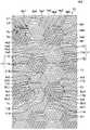
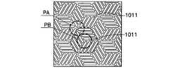
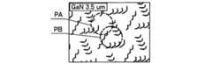
次に、基板の特徴について説明する。図10A〜図10Dに示すように、第1ユニットKUのみでユニット中央の凸部11の配置を狭くした状態のユニットパターンと、図11A〜図11Dに示すように、第1ユニットKUと鏡面対称となる第2ユニットTUを配置してユニット中央の配置を広くした状態のユニットパターンと、の場合において、結晶成長の過程における平坦度を比較して説明する。なお、図10A〜図10Dでは、PBの領域で中央の凸部1011の端部の間隔が狭く、各m軸方向に連続する領域が小さくなった状態(接線Ya1〜Ya3を凸部11の端部が越えている状態)としている。そして、図10A〜図10Dでは、比較例として、凸部1011を設けたサファイア基板上にGaNを成長させた例として、走査型電子顕微鏡(SEM)写真を元に作成した模式図を参照して説明する。また、図11A〜図11Dは、実施形態1として、長尺状の凸部11を設けたサファイア基板上にGaNを成長させた例として、走査型電子顕微鏡(SEM)写真を参考に作成した模式図を参照して説明する。  Next, features of the substrate will be described. As shown in FIGS. 10A to 10D, a unit pattern in which the arrangement of theprojections 11 at the center of the unit is narrowed only by the first unit KU and mirror-symmetric with the first unit KU as shown in FIGS. 11A to 11D. In the case of the unit pattern in which the second unit TU is arranged and the unit center is widened, the flatness in the crystal growth process is compared and described. 10A to 10D, in the PB region, the interval between the end portions of the centralconvex portion 1011 is narrow, and the regions continuous in the m-axis direction are small (the tangents Ya1 to Ya3 are the ends of the convex portion 11). Part is over). 10A to 10D, as comparative examples, refer to schematic diagrams created based on scanning electron microscope (SEM) photographs as examples of growing GaN on a sapphire substrate provided withconvex portions 1011. explain. In addition, FIGS. 11A to 11D are schematic diagrams created by referring to a scanning electron microscope (SEM) photograph as an example in which GaN is grown on a sapphire substrate provided with along projection 11 as Embodiment 1. FIG. This will be described with reference to the drawings.

凸部11及び凸部1011はそれぞれ、長手方向の長さが約10μmであり、短手方向の長さが約2.6μmであり、高さが約1.4μmである。凸部11及び凸部1011は、長手方向に延びる外縁がサファイア基板の第1のm軸Sa1、第2のm軸Sa2、第3のm軸Sa3の方向に沿って延伸して形成されており、GaNの膜厚は、図10B及び図11Bにおいて約2μmであり、図10C及び図11Cにおいて約3.5μmであり
、図10D及び図11Dにおいて約4.5μmである。なお、GaNは、ガリウム原料ガスであるTMGを供給する流量を、例えば、膜厚が2μm程度になるまで20sccm、それ以降を60sccmにして成膜する。他のプロセス条件としては、GaNの膜厚が2μm程度になるまで、圧力を1気圧、V/III比は2000程度とし、それ以降は、圧力を1気圧、V/III比を1500程度とする。また、+c面を主面とするサファイア基板を用いており、このサフィイア基板の主面に、バッファ層としてAlGaNを膜厚が20nm程度となるように成膜した後、GaNを成膜する。
Each of theconvex portion 11 and theconvex portion 1011 has a length in the longitudinal direction of about 10 μm, a length in the lateral direction of about 2.6 μm, and a height of about 1.4 μm. Theconvex portion 11 and theconvex portion 1011 are formed such that outer edges extending in the longitudinal direction extend along the direction of the first m-axis Sa1, the second m-axis Sa2, and the third m-axis Sa3 of the sapphire substrate. The film thickness of GaN is about 2 μm in FIGS. 10B and 11B, about 3.5 μm in FIGS. 10C and 11C, and about 4.5 μm in FIGS. 10D and 11D. Note that GaN is formed by setting the flow rate of supplying TMG, which is a gallium source gas, to, for example, 20 sccm until the film thickness reaches about 2 μm and 60 sccm thereafter. As other process conditions, the pressure is 1 atm and the V / III ratio is about 2000 until the film thickness of GaN is about 2 μm, and thereafter, the pressure is 1 atm and the V / III ratio is about 1500. . Further, a sapphire substrate having a + c plane as a main surface is used, and AlGaN is formed as a buffer layer on the main surface of the sapphire substrate so as to have a thickness of about 20 nm, and then GaN is formed.

図中のPAで示す位置と、PBで示す位置との状態を比較すると、次のようなことが分かる。すなわち、図10B〜図10Dでは、第1ユニットKUのみで、かつ、ユニット中央で凸部1011が密集した状態であるため、GaNの結晶成長による膜厚が4.5μmの状態が、PA及びPBの位置において異なっている。つまり、図10Dに示すように、PAの位置では、結晶成長が早く既に平坦になっているが、PBの位置では成長し易いGaNの±a軸方向(サファイア基板の±m軸方向)にスペースが無いために、結晶成長がPAの位置よりも遅いことでまだ凹状である。  Comparing the state indicated by PA and the position indicated by PB in the figure, the following can be understood. That is, in FIGS. 10B to 10D, since only the first unit KU and theconvex portions 1011 are densely arranged at the center of the unit, the state where the film thickness by the GaN crystal growth is 4.5 μm is PA and PB. Are different in position. That is, as shown in FIG. 10D, at the position of PA, the crystal growth is already fast and flat, but at the position of PB, the GaN easily grows in the ± a axis direction (± m axis direction of the sapphire substrate). Since the crystal growth is slower than the position of PA, it is still concave.

一方、図11Aでは、ユニット中央の凸部11の端部同士が間隔を空けている状態(接線Ya1〜Ya3を凸部11の端部が越えていない状態)で、第1ユニットKU及び第2ユニットTUによるユニットパターンであるため、図11B〜図11Dに示すように、GaNの成長膜厚が4.5μmの位置では、PA及びPBの位置において、ほぼ平坦な状態に整っている。つまり、ユニット中央において、GaNの±a軸方向(サファイア基板の±m軸方向)にスペースが有ることと、第1ユニット及び第2ユニットのユニットパターンを用いていることにより、基板全体の成長速度が略同じ状態となり、GaNを凹凸状態がより少なくなるように成長させた平坦な構成にできる。  On the other hand, in FIG. 11A, the first unit KU and the second unit in the state where the ends of theprotrusions 11 at the center of the unit are spaced apart (the tangents Ya1 to Ya3 do not exceed the ends of the protrusions 11). Since the unit pattern is a unit TU, as shown in FIGS. 11B to 11D, the GaN growth film thickness is 4.5 μm, and the PA and PB positions are almost flat. That is, at the center of the unit, there is a space in the ± a-axis direction of GaN (± m-axis direction of the sapphire substrate), and the unit pattern of the first unit and the second unit is used, so that the growth rate of the entire substrate Are substantially in the same state, and a flat structure can be obtained in which GaN is grown so as to have less unevenness.

次に、比較例として、図10AのPBに示される配置の凸部11が形成されたサファイア基板に、窒化物半導体層を成長させたウェハを準備する。さらに、実施例として、図11AのPBに示される配置の凸部1011が形成されたサファイア基板に窒化物半導体層を成長させたウェハを準備する。準備した比較例のウェハと実施例のウェハのそれぞれ中央領域において、(002)面のXRC半値幅と、貫通転位に起因したピット数とを測定し、それらの値を表1に示す。  Next, as a comparative example, a wafer is prepared by growing a nitride semiconductor layer on a sapphire substrate on which theprotrusions 11 having the arrangement shown in PB of FIG. 10A are formed. Further, as an example, a wafer is prepared in which a nitride semiconductor layer is grown on a sapphire substrate on whichconvex portions 1011 having the arrangement shown in PB of FIG. 11A are formed. Table 1 shows the XRC half-value width of the (002) plane and the number of pits due to threading dislocations in the respective central regions of the prepared comparative example wafer and the example wafer.

また、比較例及び実施例のいずれにおいても、(002)面のXRC半値幅を測定する場合は、図10C又は図11C上に、さらにn型半導体層、活性層、p型半導体層を順に成長させた窒化物半導体層を測定している。
そして、貫通転位に起因したピット数を測定する場合は、図10C又は図11C上にn型半導体層を成長させた窒化物半導体層に、さらに測定のためのGaNを成長させた状態で、窒化物半導体層の上面から10μm×10μmの範囲を測定している。なお、このピット数の測定において、n型半導体層上にさらに成長させたGaNは、転位密度を簡易的に測定するために、わざと横方向成長が遅くなる条件で成長させ、転位を起点としたピットを生じさせることによって、窒化物半導体層の上面から当該転位をピットとして目視できるようにしたものである。
In both the comparative example and the example, when measuring the XRC half-value width of the (002) plane, an n-type semiconductor layer, an active layer, and a p-type semiconductor layer are further grown in order on FIG. 10C or FIG. 11C. The nitride semiconductor layer is measured.
When measuring the number of pits due to threading dislocations, the nitride semiconductor layer on which the n-type semiconductor layer is grown on FIG. 10C or FIG. 11C is further nitrided with GaN for measurement grown. A range of 10 μm × 10 μm from the upper surface of the physical semiconductor layer is measured. In this measurement of the number of pits, the GaN further grown on the n-type semiconductor layer was grown on the condition that the lateral growth was intentionally slowed in order to easily measure the dislocation density. By generating pits, the dislocations can be seen as pits from the upper surface of the nitride semiconductor layer.

Figure 0006135751
Figure 0006135751

表1に示すように、図10Aで示す凸部1011の構成を備える比較例よりも、図11Aで示す凸部11の構成を備える実施例の方が、(002)面のXRC半値幅の値が小さく、さらに貫通転位に起因のピット数から転位密度も少ないことが分かる。  As shown in Table 1, the value of the XRC half-value width of the (002) plane is higher in the example having the configuration of theconvex portion 11 shown in FIG. 11A than in the comparative example having the configuration of theconvex portion 1011 shown in FIG. 10A. From the number of pits due to threading dislocations, the dislocation density is low.

次に、比較例として図10Aで示す凸部1011の構成を有するサファイア基板、及び、実施例として図11Aで示す凸部11の構成を有するサファイア基板に、それぞれGaNを成長させてn型半導体層、活性層、p型半導体層を順に積層したウェハを個片化して、発光素子を採取する。採取した比較例と実施例のそれぞれの発光素子において、順方向電圧(Vf)と、光出力(Po)と、電力変換効率(WPE)と、温度特性とを測定し、それらの値を表2に示す。なお、表2に示される値は、比較例及び実施例のいずれも、ウェハの中央領域から採取した発光素子に電極を形成したサンプルを測定した値である。
また、温度特性は、発光素子に65mAの電流を流して雰囲気温度を100℃としたときの光出力(Po)と、25℃としたときの光出力(Po)とから、以下の数式1により算出する。この温度特性の値が高いほど温度変化に対する光出力の低下が少ない(温度特性がよい)ことになる。
Next, GaN is grown on the sapphire substrate having the configuration of theconvex portion 1011 shown in FIG. 10A as a comparative example and the sapphire substrate having the configuration of theconvex portion 11 shown in FIG. Then, the wafer in which the active layer and the p-type semiconductor layer are sequentially laminated is separated into individual pieces, and the light emitting element is collected. In each of the collected light emitting elements of the comparative example and the example, the forward voltage (Vf), the light output (Po), the power conversion efficiency (WPE), and the temperature characteristic were measured, and the values are shown in Table 2. Shown in In addition, the value shown in Table 2 is a value obtained by measuring a sample in which an electrode is formed on a light emitting element taken from the central region of the wafer in both the comparative example and the example.
Further, the temperature characteristics are expressed by the following formula 1 from the light output (Po) when the ambient temperature is set to 100 ° C. by flowing a current of 65 mA to the light emitting element and the light output (Po) when the temperature is set to 25 ° C. calculate. The higher the value of this temperature characteristic, the smaller the decrease in light output with respect to temperature change (the temperature characteristic is better).

Figure 0006135751
Figure 0006135751

Figure 0006135751
Figure 0006135751

表2に示すように、図10Aで示す凸部1011を有する比較例の発光素子よりも、図11Aで示す凸部11を有する実施例の発光素子の構成の方が、順方向電圧(Vf)の値が小さく、光出力(Po)の値が大きく、電力変換効率(WPE)の値も高く、かつ、温度特性の値が大きいことが分かる。つまり、本開示のような構成とする発光素子1では、結晶配向も改善されることによって、温度特性を維持又は改善しつつ、順方向電圧(Vf)を低下させ、光出力(Po)は向上させることができる。これに伴って、発光素子1は、発光効率も良くなる構成であるといえる。  As shown in Table 2, the forward voltage (Vf) of the configuration of the light emitting element of the example having theconvex portion 11 shown in FIG. 11A is more than that of the light emitting element of the comparative example having theconvex portion 1011 shown in FIG. 10A. It can be seen that the value of is small, the value of optical output (Po) is large, the value of power conversion efficiency (WPE) is high, and the value of the temperature characteristic is large. That is, in the light-emitting element 1 configured as in the present disclosure, the crystal orientation is also improved, so that the forward voltage (Vf) is reduced and the light output (Po) is improved while maintaining or improving the temperature characteristics. Can be made. Accordingly, it can be said that the light emitting element 1 has a configuration in which the light emission efficiency is improved.

以上のように、第1実施形態に係る発光素子1及びその製造方法について、具体的に説明したが、本開示の趣旨はこれらの記載に限定されるものではなく、特許請求の範囲の記載に基づいて広く解釈されなければならない。また、これらの記載に基づいて種々変更、改変等したものも本発明の趣旨に含まれることはいうまでもない。
以下では、第2〜第4実施形態及び変形例1〜3について図12〜図17を参照して図面で説明する。なお、図12〜図16は、凸部の配置の構成について、第1実施形態と異なる部分を主に説明する。また、以下で説明する第2〜第4実施形態に係る発光素子は、サファイア基板の凸部以外の構成及び製造方法については第1実施形態に係る発光素子1と同様であるため、それらの説明は省略する。
As described above, the light-emitting element 1 and the manufacturing method thereof according to the first embodiment have been specifically described. However, the gist of the present disclosure is not limited to these descriptions, and the description of the claims. Should be widely interpreted on the basis. Needless to say, various changes and modifications based on these descriptions are also included in the spirit of the present invention.
Below, 2nd-4th embodiment and the modifications 1-3 are demonstrated with drawing with reference to FIGS. 12-17. FIGS. 12 to 16 mainly describe portions different from the first embodiment with respect to the arrangement of the convex portions. Moreover, since the light-emitting elements according to the second to fourth embodiments described below are the same as the light-emitting element 1 according to the first embodiment with respect to the configuration and the manufacturing method other than the convex portion of the sapphire substrate, the description thereof is omitted. Is omitted.

<第2実施形態>
図12に示すように、第2実施形態で示す発光素子の第1凸部11A〜第3凸部11Cでは、第1間隔da1〜第3間隔da3及び第4間隔ds1〜第6間隔ds3を、図3で示す構成よりも大きくとり、かつ、第1凸部11A〜第3凸部11Cのそれぞれの間隔も広くしている。このように構成された発光素子は、サファイア基板10Aの第1凸部11A〜第3凸部11Cが、第1ユニットKU及び第2ユニットTUのユニットパターンで、かつ、図3で示す構成よりも各間隔が20〜40%の範囲で広く構成されているので、半導体層が成長したときに平坦性をより確保し易くなる。なお、図3で示す凸部11の間隔が、例えば、3μmを基準とした場合であれば、図12に示す凸部11の間隔は、3.6〜4.2μmである。なお、各間隔が20〜40%の範囲で広くとは、許容範囲内において、平均的な値を基準値とした場合、その基準値の20〜40%広くしたことをいう。つまり、各間隔は、基準値に対して許容範囲内の上限側に設定されていることが好ましい。
Second Embodiment
As shown in FIG. 12, in the firstconvex portion 11A to the thirdconvex portion 11C of the light emitting element shown in the second embodiment, the first interval da1 to the third interval da3 and the fourth interval ds1 to the sixth interval ds3 are It is larger than the configuration shown in FIG. 3, and the intervals between the firstconvex portion 11A to the thirdconvex portion 11C are also widened. In the light emitting element configured as described above, the firstconvex portion 11A to the thirdconvex portion 11C of thesapphire substrate 10A are unit patterns of the first unit KU and the second unit TU, and the configuration shown in FIG. Since each space | interval is comprised widely in 20 to 40% of range, when a semiconductor layer grows, it becomes easier to ensure flatness. In addition, if the space | interval of theconvex part 11 shown in FIG. 3 is a case on the basis of 3 micrometers, for example, the space | interval of theconvex part 11 shown in FIG. 12 is 3.6-4.2 micrometers. In addition, when each interval is 20 to 40% in a wide range, when an average value is set as a reference value within an allowable range, it means that the interval is increased by 20 to 40% of the reference value. In other words, each interval is preferably set on the upper limit side within an allowable range with respect to the reference value.

以上のような構成を備える第2実施形態に係る発光素子は、サファイア基板10A上に配置された凸部11の長手方向の外縁が、サファイア基板10Aの各m軸に沿って延伸して配置され設置間隔も基準値となるものよりも20〜40%広く形成されているため、窒化物半導体の結晶成長の際に窒化物半導体が横方向に成長する時間が長くなる。これにより、窒化物半導体の結晶成長時に発生した転位が狭い範囲に収束しやすくなり、窒化物半導体層30の転位密度が低くなる。さらに、第2実施形態に係る発光素子は、結晶配向も改善され、温度特性を維持又は改善しつつ、順方向電圧(Vf)を低下させ、光出力(Po)は向上させることができ、これに伴って、発光効率も良くなる。  In the light emitting device according to the second embodiment having the above-described configuration, the outer edge in the longitudinal direction of theconvex portion 11 arranged on thesapphire substrate 10A is arranged extending along each m-axis of thesapphire substrate 10A. Since the installation interval is 20 to 40% wider than the reference value, the time during which the nitride semiconductor grows in the lateral direction becomes longer during the crystal growth of the nitride semiconductor. Thereby, the dislocations generated during the crystal growth of the nitride semiconductor are easily converged in a narrow range, and the dislocation density of thenitride semiconductor layer 30 is lowered. Furthermore, the light emitting device according to the second embodiment has improved crystal orientation, and can maintain or improve temperature characteristics while reducing the forward voltage (Vf) and improving the light output (Po). As a result, the luminous efficiency is improved.

<第3実施形態>
図13に示すように、第3実施形態に係る発光素子のサファイア基板10Bを平面視すると、サファイア基板10Bのc面側の表面において、仮想的に示す菱形の各領域には凸部111が長手方向の外縁を各m軸に沿って延伸させて3本ずつ配置されている。凸部111は、具体的には、長尺形状の長手方向の外縁が第1のm軸Sa1に沿って延伸して配置される第1凸部111Aと、長尺形状の長手方向の外縁が第2のm軸Sa2に沿って延伸して配置される第2凸部111Bと、長尺形状の長手方向の外縁が第3のm軸Sa3に沿って延伸して配置される第3凸部111Cと、から構成される。
<Third Embodiment>
As shown in FIG. 13, when thesapphire substrate 10B of the light emitting device according to the third embodiment is viewed in plan, theconvex portion 111 is elongated in each region of the rhombus virtually shown on the surface on the c-plane side of thesapphire substrate 10B. Three outer edges in the direction are extended along each m-axis. Specifically, theconvex portion 111 includes a firstconvex portion 111A in which the outer edge of the elongated shape in the longitudinal direction is arranged along the first m-axis Sa1, and the outer edge of the elongated shape in the longitudinal direction. The secondconvex portion 111B arranged to extend along the second m-axis Sa2, and the third convex portion arranged so that the outer edge in the longitudinal direction of the elongated shape extends along the third m-axis Sa3. 111C.

ここで、第1凸部111A〜第3凸部111Cでは、各凸部間の間隔が当該凸部のコア径と同等か、それ以上となるように設定されている。なお、凸部111のピッチ(凸部のコア径中心に凸部長手方向に沿って中心線を引いたときに、隣の凸部の当該中心線までの距離)Pcは、コア径Daを越えるように設定されている。第1凸部111A〜第3凸部111Cでは、凸部間の間隔及びピッチPcが広く、また、第1間隔da1〜第3間隔da3及び第4間隔ds1〜第6間隔ds3の間隔も凸部間の間隔に合せて広く設定されている。第1凸部111A〜第3凸部111Cは、一例として、コア径Daとコア全長L1との比が1対5〜6となるようにここでは設定されている。また、コア径DaとピッチPcとの関係は、一例として、1対2となるように設定されている。  Here, in 1stconvex part 111A-3rdconvex part 111C, the space | interval between each convex part is set so that it may become equal to or more than the core diameter of the said convex part. Note that the pitch Pc of the convex portions 111 (the distance to the central line of the adjacent convex portion when a center line is drawn along the longitudinal direction of the convex portion at the center of the core diameter of the convex portion) Pc exceeds the core diameter Da. Is set to In the firstconvex portion 111A to the thirdconvex portion 111C, the interval between the convex portions and the pitch Pc are wide, and the first interval da1 to the third interval da3 and the fourth interval ds1 to the sixth interval ds3 are also convex portions. Widely set according to the interval between them. As an example, the firstconvex portion 111A to the thirdconvex portion 111C are set so that the ratio of the core diameter Da to the total length L1 of the core is 1 to 5-6. Further, the relationship between the core diameter Da and the pitch Pc is set to be 1 to 2, as an example.

以上のような構成を備える第3実施形態に係る発光素子は、サファイア基板10B上に形成された凸部111と凸部111が形成されていない平坦部分との間隔がより適切であるので、結晶成長の際に窒化物半導体が横方向に成長する時間が長くなり、結晶成長時に発生した転位が狭い範囲に収束しやすくなり、窒化物半導体層30の転位密度が低くなる。さらに、第3実施形態に係る発光素子は、結晶配向も改善され、温度特性を維持又は改善しつつ、順方向電圧(Vf)を低下させ、光出力(Po)は向上させることができ、これに伴って、発光効率も良くなる。  In the light emitting device according to the third embodiment having the above-described configuration, the distance between theconvex portion 111 formed on thesapphire substrate 10B and the flat portion where theconvex portion 111 is not formed is more appropriate. During the growth, the time for the nitride semiconductor to grow in the lateral direction becomes longer, dislocations generated during crystal growth tend to converge in a narrow range, and the dislocation density of thenitride semiconductor layer 30 becomes lower. Furthermore, the light emitting device according to the third embodiment has improved crystal orientation, and can maintain or improve temperature characteristics while reducing the forward voltage (Vf) and increasing the light output (Po). As a result, the luminous efficiency is improved.

<第4実施形態>
図14に示すように、第4実施形態に係る発光素子のサファイア基板10Cを平面視すると、サファイア基板10Cのc面側の表面において、仮想的に示す菱形の領域内には各m軸にそれぞれ延伸して所定間隔で5本の凸部211が配置されている。第1ユニットの凸部211は、具体的には、長尺形状の長手方向の外縁が第1のm軸Sa1に沿って延伸する第1凸部211Aと、長尺形状の長手方向の外縁が第2のm軸Sa2に沿って延伸する第2凸部211Bと、長尺形状の長手方向の外縁が第3のm軸Sa3に沿って延伸する第3凸部211Cと、から構成される。第1凸部211A〜第3凸部211Cは、コア径Daとコア全長L1との比が1対11.5となっており、コア径DaとピッチPcとの比は1対2.5となるように設定されている。
<Fourth embodiment>
As shown in FIG. 14, when thesapphire substrate 10 </ b> C of the light emitting device according to the fourth embodiment is viewed in plan, on the surface of thesapphire substrate 10 </ b> C on the c-plane side, The fiveconvex portions 211 are arranged at predetermined intervals by extending. Specifically, theconvex portion 211 of the first unit has a long convex outer edge in the longitudinal direction extending along the first m-axis Sa1, and a long convex outer edge in the longitudinal direction. A secondconvex portion 211B extending along the second m-axis Sa2 and a thirdconvex portion 211C having an elongated outer edge extending along the third m-axis Sa3 are configured. In the firstconvex portion 211A to the thirdconvex portion 211C, the ratio of the core diameter Da to the total length L1 of the core is 1 to 11.5, and the ratio of the core diameter Da to the pitch Pc is 1 to 2.5. It is set to be.

このように、凸部211は、コア径Daとコア全長L1との比が図3で示す構成よりも小さくなっても、第1ユニットKUと第2ユニットTUとによるユニットパターン、及び、ユニット中央部分の間隔を空ける構成としている。そのため、前記したものと同様に、発光素子において、結晶配向も改善され、温度特性を維持又は改善しつつ、Vfを低下させ、光出力は向上させることができ、これに伴って、発光効率も良くなる。
なお、第2実施形態〜第4実施形態では、仮想的に示す菱形の各領域内において、凸部の数を3〜5本とした構成について説明したが、6本あるいは7本以上であってもよい。
Thus, even if the ratio of the core diameter Da and the core total length L1 becomes smaller than the structure shown in FIG. 3, theconvex part 211 has the unit pattern by the 1st unit KU and the 2nd unit TU, and the unit center. The configuration is such that the portions are spaced apart. Therefore, similar to the above, in the light emitting element, the crystal orientation is also improved, and while maintaining or improving the temperature characteristics, Vf can be reduced and the light output can be improved, and accordingly, the light emission efficiency is also improved. Get better.
In addition, in 2nd Embodiment-4th Embodiment, in each area | region of the rhombus shown virtually, although the structure which made the number of convex parts 3-5 was demonstrated, it is 6 or 7 or more, Also good.

また、前記した第1実施形態〜第4実施形態に係る窒化物半導体素子のサファイア基板10〜10Cは、長尺形状の凸部11、111,211の両端が揃った配列として説明したが、例えば、図15〜図17に示すように、その一部あるいは全部の両端の位置が異なるように第1領域Ar1〜第3領域Ar3の内部において配置されていてもよい。ここでは、図3のサファイア基板10の凸部11の構成を代表して説明するが他の実施形態でも同様の作用効果が生じる。また、ここでは、第3凸部11Cの第1ユニットKUにおいて中心に最も近い凸部の位置を変更した例として説明するが、第3凸部11Cの他のもの、あるいは、第1凸部11A又は第2凸部11Bの一部であってもよい。  Moreover, although thesapphire substrates 10 to 10C of the nitride semiconductor elements according to the first to fourth embodiments described above have been described as an array in which both ends of the elongatedconvex portions 11, 111, and 211 are aligned, As shown in FIGS. 15 to 17, the first and second regions Ar <b> 1 to Ar <b> 3 may be arranged so that the positions of some or all of the both ends are different. Here, the configuration of theconvex portion 11 of thesapphire substrate 10 in FIG. 3 will be described as a representative, but the same function and effect are produced in other embodiments. In addition, here, an example in which the position of the convex portion closest to the center in the first unit KU of the thirdconvex portion 11C is changed will be described, but the other one of the thirdconvex portion 11C or the firstconvex portion 11A. Or a part of 2ndconvex part 11B may be sufficient.

<変形例1>
図15に示すように、第1ユニットKUの第1凸部11A〜第3凸部11Cは、その一部として、例えば、第3凸部11Cの1つの端部が他のものと異なるように配置する凸部11d(ハッチングを施した凸部)を備える構成としてもよい。そして、この凸部11dは、第1ユニットKUのみに形成され、第2ユニットTUには形成されないように構成されている。つまり、第2ユニットTUは、第1領域Ar1〜第3領域Ar3の配置が鏡面対称となることが必要で、その領域内に配置される凸部11dを含む第1凸部11A〜第3凸部11Cの配置を鏡面対称としていない。
<Modification 1>
As shown in FIG. 15, the firstconvex portion 11 </ b> A to the thirdconvex portion 11 </ b> C of the first unit KU are, for example, such that one end of the thirdconvex portion 11 </ b> C is different from the other. It is good also as a structure provided with theconvex part 11d (convex part which gave the hatching) to arrange | position. And thisconvex part 11d is formed only in the 1st unit KU, and it is comprised so that it may not be formed in the 2nd unit TU. That is, in the second unit TU, the arrangement of the first area Ar1 to the third area Ar3 needs to be mirror-symmetrical, and thefirst protrusion 11A to the third protrusion including theprotrusion 11d arranged in the area. The arrangement of thepart 11C is not mirror-symmetric.

そして、図15で示すように、凸部11dを含む第1凸部11A〜第3凸部11Cの配置の第1ユニットKUと、凸部11dを含まない第1凸部11A〜第3凸部11Cの配置の第2ユニットTUと、からなるユニットパターンであっても、全体的に見れば、第1ユニットKUを中心とする単位で同一なパターンを繰り返す状態となる。また、凸部11dは、第1ユニットKUの中心に最も近い第3凸部11Cの位置を他の第3凸部11Cから異ならせたものであり、接線Ya1に当接して交わるように配置されている。ただし、第2間隔da2が第2領域Ar2から第1領域Ar1に連続しているので、第1ユニットKUの中央における領域は広く確保されることになる。したがって、前記したように、このようなサファイア基板10の凸部11dを含む凸部11であっても、第1ユニットKU及び第2ユニットTUのユニットパターンと、ユニット中央部分での領域の構成を備えることで、前記したものと同様に、従来の構成と比較して、発光素子において、結晶配向も改善され、温度特性を維持又は改善しつつ、順方向電圧(Vf)を低下させ、光出力(Po)は向上させることができ、これに伴って、発光効率も良くなる。  And as shown in FIG. 15, 1st unit 11K of arrangement | positioning of the 1stconvex part 11A-3rdconvex part 11C including theconvex part 11d, and the 1stconvex part 11A-3rd convex part which does not contain theconvex part 11d Even if the unit pattern is composed of the second unit TU having the arrangement of 11C, the same pattern is repeated in units centered on the first unit KU as a whole. Further, theconvex portion 11d is obtained by making the position of the thirdconvex portion 11C closest to the center of the first unit KU different from the other thirdconvex portion 11C, and is arranged so as to abut on the tangent line Ya1. ing. However, since the second interval da2 is continuous from the second region Ar2 to the first region Ar1, a region in the center of the first unit KU is secured widely. Therefore, as described above, even in theconvex portion 11 including theconvex portion 11d of thesapphire substrate 10, the unit pattern of the first unit KU and the second unit TU and the configuration of the region in the central portion of the unit. In the same manner as described above, in the light emitting device, the crystal orientation is improved and the forward voltage (Vf) is reduced while maintaining or improving the temperature characteristics, as compared with the conventional structure, and the light output (Po) can be improved, and the luminous efficiency is improved accordingly.

<変形例2>
また、図16に示すように、第1ユニットKU及び第2ユニットTUにおいて、第3凸部11Cの1つを凸部11e(ハッチングを施した凸部)として、端部が他の第3凸部11Cと異なるように配置した構成としても構わない。ここでは、凸部11eの配置を含めて、第1ユニットKUの鏡面対称に第2ユニットTUが構成されている。このように、第1ユニットKU及び第2ユニットTUにおいて端部の位置が他のものと異なるような凸部11eが存在しても、全体的に見れば、第1ユニットKUの各辺に第2ユニットTUの辺が合わさるユニットパターンの単位毎においては、均等な配置となる。したがって、前記したように、このようなサファイア基板10の凸部11eを含む凸部11であっても、第1ユニットKU及び第2ユニットTUのユニットパターンと、ユニット中央部分での領域の構成を備えることで、前記したものと同様に、従来の構成と比較して、発光素子において、結晶配向も改善され、温度特性を維持又は改善しつつ、順方向電圧(Vf)を低下させ、光出力(Po)は向上させることができ、これに伴って、発光効率も良くなる。
<Modification 2>
In addition, as shown in FIG. 16, in the first unit KU and the second unit TU, one of the thirdconvex portions 11C is defined as aconvex portion 11e (hatched convex portion), and the end portion is another third convex portion. The configuration may be different from that of thepart 11C. Here, the second unit TU is configured with mirror symmetry of the first unit KU including the arrangement of theconvex portions 11e. In this way, even if there is aconvex portion 11e whose end portion is different from the other ones in the first unit KU and the second unit TU, on the whole, the first unit KU has a first portion KU on each side. In the unit pattern unit in which the sides of the two units TU are combined, the arrangement is equal. Therefore, as described above, even in theconvex portion 11 including theconvex portion 11e of thesapphire substrate 10, the unit pattern of the first unit KU and the second unit TU and the configuration of the region in the central portion of the unit. In the same manner as described above, in the light emitting device, the crystal orientation is improved and the forward voltage (Vf) is reduced while maintaining or improving the temperature characteristics, as compared with the conventional structure, and the light output (Po) can be improved, and the luminous efficiency is improved accordingly.

<変形例3>
さらに、図17に示すように、第1ユニットKUは、第1領域Ar1の領域内において配置される第1凸部11Aと、第2領域の領域内において配置される第2凸部11Bと、第3領域Ar3の領域内において配置される第3凸部11Cとが、領域ごとに異なる配置となるように構成しても構わない。なお、図17において、第1間隔da1〜第3間隔da3は、最大の間隔の幅を示している。また、ユニットパターンとしては、第1ユニットKUの第1凸部11A〜第3凸部11Cの配置が鏡面対称となる第2ユニットTUの一辺を、第1ユニットKUの各辺に合せて配置する構成としてもよい。さらに、第1ユニットの第1凸部11A〜第3凸部11Cの配置とは異なる、例えば、図3に示す構成の第2ユニットTUを図17の第1ユニットKUの各辺に配置するように構成しても構わない。
<Modification 3>
Further, as shown in FIG. 17, the first unit KU includes a firstconvex portion 11A disposed in the region of the first region Ar1, a secondconvex portion 11B disposed in the region of the second region, You may comprise so that the 3rdconvex part 11C arrange | positioned in the area | region of 3rd area | region Ar3 may become arrangement | positioning different for every area | region. In FIG. 17, the first interval da1 to the third interval da3 indicate the width of the maximum interval. Further, as the unit pattern, one side of the second unit TU in which the arrangement of the firstconvex portion 11A to the thirdconvex portion 11C of the first unit KU is mirror-symmetric is arranged according to each side of the first unit KU. It is good also as a structure. Further, for example, the second unit TU having the configuration shown in FIG. 3 is arranged on each side of the first unit KU in FIG. 17, which is different from the arrangement of thefirst protrusions 11 </ b> A to 11 </ b> C of the first unit. You may comprise.

図17に示すように、第1ユニットKUの第1凸部11A〜第3凸部11Cのそれぞれの端部が異なるように構成されていても、第1ユニットKU及びその第1ユニットKUを中心として配置される第2ユニットTUのユニット単位毎においては、同じ凸部11の配置の繰り返しとなる。したがって、前記したように、このようなサファイア基板10の凸部11の配置であっても、第1ユニットKU及び第2ユニットTUのユニットパターンと、ユニット中央部分での領域の構成を備えることで、前記したものと同様に、従来の構成と比較して、発光素子において、結晶配向も改善され、温度特性を維持又は改善しつつ、、順方向電圧(Vf)を低下させ、光出力(Po)は向上させることができ、これに伴って、発光効率も良くなる。  As shown in FIG. 17, the first unit KU and the first unit KU are centered even if the end portions of the firstconvex portion 11A to the thirdconvex portion 11C of the first unit KU are different from each other. In each unit unit of the second unit TU arranged as, the sameconvex portion 11 is repeatedly arranged. Therefore, as described above, even with such an arrangement of theconvex portions 11 of thesapphire substrate 10, the unit pattern of the first unit KU and the second unit TU and the configuration of the region at the center portion of the unit are provided. As described above, the crystal orientation is improved in the light emitting device as compared with the conventional structure, and the forward voltage (Vf) is reduced while maintaining or improving the temperature characteristics, and the light output (Po) is reduced. ) Can be improved, and with this, the luminous efficiency is improved.

以上説明した各実施形態における発光素子では以下のような構成としてもよい。すなわち、サファイア基板では、凸部は、第1領域Ar1〜第3領域Ar3に各m軸に沿って配置することができれば、図3、図12〜図17で示したように、凸部の端部が揃っていても、一部あるいは全く揃っていなくても構わない。つまり、第1ユニットKUは、正六角形の中心に最も近い3つの凸部の内の2つが、対向する接線Ya1〜Ya3のいずれかに交わり合うことなく離間して配置されて、かつ、他の凸部は第1間隔da1〜第3間隔da3を形成するように配置されていれば構わない。そして、第1ユニットKU及びその鏡面対称となる第2ユニットTUのユニットパターンを用いていれば既に説明したような、発光素子において、順方向電圧(Vf)の値が低くなり、温度特性が向上し、電力変換効率(WPE)も向上させることができる。
また、第1ユニットと第2ユニットとによるユニットパターンは、第2ユニットの正六角形の各辺に第1ユニットの正六角形の辺を合せて配置させた構成としてもよい。
The light emitting element in each embodiment described above may have the following configuration. That is, in the sapphire substrate, if the protrusions can be arranged along the m-axis in the first region Ar1 to the third region Ar3, as shown in FIGS. It does not matter if the parts are aligned, or part or not at all. That is, the first unit KU is arranged such that two of the three convex portions closest to the center of the regular hexagon are separated from each other without intersecting any of the opposing tangent lines Ya1 to Ya3, and the other The convex portions may be arranged so as to form the first interval da1 to the third interval da3. Then, if the unit pattern of the first unit KU and the second unit TU that is mirror-symmetrical to the first unit KU is used, in the light emitting device, the value of the forward voltage (Vf) is lowered and the temperature characteristics are improved. In addition, power conversion efficiency (WPE) can be improved.
The unit pattern of the first unit and the second unit may be configured such that the regular hexagonal sides of the first unit are aligned with the regular hexagonal sides of the second unit.

なお、サファイア基板において、各m軸に沿って各ユニット単位で配置した凸部11としているので、長手方向の延長線上に別の凸部11が配置されることになり、光の横漏れを抑制し、ランバーシアンに近い配光特性を得ることができる。
なお、図3、図12〜図17では、凸部11,111,211において、両端が半円形で略同一形状に形成されているが、凸部11,111,211の形状はこれに限定されない。
さらに、凸部11,111,211は、c面から上方向に突出して、高さ方向の所定位置から稜線に対して角度θとなるように傾斜面を介して尖って形成される構成であってもよい。これにより、前記した凸部11,111,211と同様に、窒化物半導体の結晶成長の際に凸部12の上部からの成長が抑制されて窒化物半導体が横方向に成長するため、成長方向に発生した複数の転位が収束し、転位の数が減少することになる。
なお、傾斜面を形成する場合には、ドライエッチングの次にウェットエッチングすることで、凸部11,111,211の頂部に向かって傾斜する傾斜面を形成することができる。
In addition, in the sapphire substrate, since it is set as theconvex part 11 arrange | positioned in each unit unit along each m-axis, anotherconvex part 11 will be arrange | positioned on the extension line | wire of a longitudinal direction, and the side leakage of light is suppressed. In addition, light distribution characteristics close to Lambertian can be obtained.
In FIGS. 3 and 12 to 17, both ends of theconvex portions 11, 111, and 211 are semicircular and substantially the same shape, but the shape of theconvex portions 11, 111, and 211 is not limited to this. .
Further, theprotrusions 11, 111, 211 are configured to protrude upward from the c-plane and be pointed through an inclined surface so as to have an angle θ with respect to the ridge line from a predetermined position in the height direction. May be. As a result, similar to theconvex portions 11, 111, 211 described above, the growth from the top of the convex portion 12 is suppressed during the crystal growth of the nitride semiconductor, and the nitride semiconductor grows in the lateral direction. A plurality of dislocations occurring in the region converge and the number of dislocations decreases.
In addition, when forming an inclined surface, the inclined surface which inclines toward the top part of theconvex parts 11, 111, 211 can be formed by performing wet etching after dry etching.

なお、発光素子1、2では、第1ユニットKU及び第2ユニットTUで、第1領域Ar1とは別の他の2つの菱形領域(第2領域Ar2及び第3領域Ar3)のうち一方の菱形領域において、第1凸部11A(111A,211A)の延伸方向に沿って端部を揃えて配置される複数の第3凸部11Cを有し、正六角形領域(第1ユニットKU及び第2ユニットTU)の中心に最も近い第3凸部11C(111C,211C)が、中心に最も近い第1凸部11A(111A,211A)における中心側の端部に接すると共に第1凸部11A(111A,211A)が配置される方向に平行をなす接線Ya3と、交わらないように配置されていることとしてもよい。  In thelight emitting elements 1 and 2, the first unit KU and the second unit TU have one rhombus of the other two rhombus regions (the second region Ar2 and the third region Ar3) different from the first region Ar1. The region has a plurality of thirdconvex portions 11C arranged with the end portions aligned along the extending direction of the firstconvex portions 11A (111A, 211A), and a regular hexagonal region (the first unit KU and the second unit). The thirdconvex portion 11C (111C, 211C) closest to the center of (TU) is in contact with the center-side end portion of the firstconvex portion 11A (111A, 211A) closest to the center and the firstconvex portion 11A (111A, 111A, 211A) may be arranged so as not to intersect the tangent line Ya3 that is parallel to the direction in which it is arranged.

さらに、前記した他の2つの菱形領域(第2領域Ar2及び第3領域Ar3)のうちの他方の菱形領域において、第3凸部11C(111C,211C)の延伸方向に沿って端部を揃えて配置される複数の第2凸部11B(111B,211B)を有し、正六角形領域(第1ユニットKU及び第2ユニットTU)の中心に最も近い第2凸部11B(111B,211B)は、前記中心に最も近い第3凸部11C(111C,211C)における中心側の端部に接すると共に第3凸部11C(111C,211C)が配置される方向に平行をなす接線と、交わらないように配置されているように前記した発光素子1、2を構成してもよい。
また、空間と間隔とは、使用される位置が異なることで、用語を分けることがあるが実質的に同意である。
Furthermore, in the other rhombus region of the other two rhombus regions (second region Ar2 and third region Ar3), the end portions are aligned along the extending direction of the thirdconvex portion 11C (111C, 211C). The secondconvex portions 11B (111B, 211B) that are closest to the center of the regular hexagonal region (first unit KU and second unit TU) The thirdconvex portion 11C (111C, 211C) closest to the center does not intersect with the tangent line that is in contact with the center side end and parallel to the direction in which the thirdconvex portion 11C (111C, 211C) is arranged. The light-emittingelements 1 and 2 described above may be configured so as to be arranged in the above.
Moreover, although space and a space | interval may use a different position and may divide terms, it is substantially agreed.

1,2 発光素子
10,10A,10B,10C,10D サファイア基板(窒化物半導体素子用基板)
11,111,211 凸部
11A,111A,211A 第1凸部
11B,111B,211B 第2凸部
11C,111C,211C 第3凸部
20 バッファ層
30 窒化物半導体層(半導体層)
31 n型半導体層
32 活性層
33 p型半導体層
40 n側電極
50 透光性電極
60 p側電極
M マスク
SC サファイア結晶
1, 2Light emitting device 10, 10A, 10B, 10C, 10D Sapphire substrate (substrate for nitride semiconductor device)
11, 111, 211convex portion 11A, 111A, 211A firstconvex portion 11B, 111B, 211B secondconvex portion 11C, 111C, 211C thirdconvex portion 20buffer layer 30 nitride semiconductor layer (semiconductor layer)
31 n-type semiconductor layer 32 active layer 33 p-type semiconductor layer 40 n-side electrode 50 translucent electrode 60 p-side electrode M mask SC sapphire crystal

Claims (9)

Translated fromJapanese
c面を主面に有するサファイア基板と、前記サファイア基板の主面側に設けられた半導
体層と、を備える発光素子であって、
前記サファイア基板は、
主面側からみて正六角形を菱形に3等分するように、第1のm軸及び第2のm軸に平行な辺で区画される第1領域と、第2のm軸及び第3のm軸に平行な辺で区画される第2領域と、第1のm軸及び第3のm軸に平行な辺で区画される第3領域とからなる第1ユニットであって、
前記第1領域内において、前記第1のm軸に平行な辺を外縁に有する複数の第1凸部が配列され、前記第2領域内において、前記第2のm軸に平行な辺を外縁に有する複数の第2凸部が配列され、前記第3領域内において、前記第3のm軸に平行な辺を外縁に有する複数の第3凸部が配列され、
前記正六角形の中心に最も近い前記第1凸部は、前記中心に最も近い前記第2凸部における前記中心側の端部に接する前記第3のm軸と平行をなす接線と交わらないように配置され、前記正六角形の中心に最も近い前記第2凸部は、前記中心に最も近い前記第3凸部における前記中心側の端部に接する前記第1のm軸と平行をなす接線と交わらないように配置された第1ユニットと
前記第1ユニットの頂角を通るa軸に対して、前記第1ユニットと鏡面対称の関係となるように前記第1領域、前記第2領域および前記第3領域が配置された第2ユニットとを有し、
前記第1のユニットおよび前記第2のユニットは、前記第1ユニットの正六角形の辺に前記第2ユニットの正六角形の辺が合うように配置されたことを特徴とする発光素子。
A light emitting device comprising: a sapphire substrate having a c-plane as a main surface; and a semiconductor layer provided on the main surface side of the sapphire substrate,
The sapphire substrate is
A first region defined by sides parallel to the first m-axis and the second m-axis, and the second m-axis and the third a first unit comprising a second region partitioned by a side parallel to the m-axis and a third region partitioned by a side parallel to the first m-axis and the third m-axis,
In the first region, a plurality of first convex portions having sides parallel to the first m-axis at the outer edge are arranged, and in the second region, the side parallel to the second m-axis is defined as an outer edge. A plurality of second convex portions having a side parallel to the third m-axis at the outer edge in the third region;
The first convex portion closest to the center of the regular hexagon does not intersect with a tangent line parallel to the third m-axis in contact with the center-side end portion of the second convex portion closest to the center. The second convex portion that is arranged and is closest to the center of the regular hexagon intersects a tangent line that is parallel to the first m-axis that is in contact with the center-side end portion of the third convex portion that is closest to the center. Afirst unit arranged so that there is no
A second unit in which the first region, the second region, and the third region are arranged so as to have a mirror-symmetrical relationship with the first unit with respect to the a-axis passing through the apex angle of the first unit; Have
The light emitting element, wherein the first unit and the second unit are arranged so that a regular hexagonal side of the first unit is aligned with a regular hexagonal side of the first unit .
前記第1凸部は、前記第2のm軸に平行な同一線上に複数の前記第1凸部の端部が揃って当該第1凸部同士が同一のピッチで配置され、前記第2凸部は、前記第3のm軸に平行な同一線上に複数の前記第2凸部の端部が揃って当該第2凸部同士が同一のピッチで配置され、前記第3凸部は、前記第1のm軸に平行な同一線上に複数の前記第3凸部の端部が揃って当該第3凸部同士が同一のピッチで配置されている請求項1に記載の発光素子。  The first convex portions are arranged such that ends of the plurality of first convex portions are aligned on the same line parallel to the second m-axis, and the first convex portions are arranged at the same pitch. The end portions of the plurality of second convex portions are aligned on the same line parallel to the third m-axis, and the second convex portions are arranged at the same pitch, and the third convex portion is 2. The light emitting device according to claim 1, wherein ends of the plurality of third convex portions are aligned on the same line parallel to the first m-axis, and the third convex portions are arranged at the same pitch. 前記第1凸部は、前記第1領域内において、前記第2領域側に所定の間隔となる第1間隔を空けて整列され、前記第2凸部は、前記第2領域内において、前記第3領域側に所定の間隔となる第2間隔を空けて整列され、前記第3凸部は、前記第3領域内において、前記第1領域側に所定の間隔となる第3間隔を空けて整列され、
前記第1間隔、前記第2間隔及び前記第3間隔が同じ間隔である請求項1又は請求項2に記載の発光素子。
The first convex portions are aligned at a first interval that is a predetermined interval on the second region side in the first region, and the second convex portions are arranged in the second region in the first region. The third protrusions are aligned with a second interval that is a predetermined interval on the three region side, and the third protrusions are aligned with a third interval that is a predetermined interval on the first region side in the third region. And
The light emitting device according to claim 1, wherein the first interval, the second interval, and the third interval are the same interval.
前記六角形の中心から最も遠い第1凸部は、前記六角形の前記第1のm軸に平行な外形線から所定の間隔となる第4間隔を空けて配置され、前記六角形の中心から最も遠い第2凸部は、前記六角形の前記第2のm軸に平行な外形線から所定の間隔となる第5間隔を空けて配置され、前記六角形の中心から最も遠い第3凸部は、前記六角形の前記第3のm軸に平行な外形線から所定の間隔となる第6間隔を空けて配置され、
前記第4間隔、前記第5間隔及び前記第6間隔が同じ間隔である請求項1から請求項3のいずれか一項に記載の発光素子。
The first convex portion farthest from the center of the hexagon is disposed at a fourth interval that is a predetermined interval from the outline parallel to the first m-axis of the hexagon, and from the center of the hexagon. The furthest second convex portion is arranged at a fifth interval, which is a predetermined interval from the outer shape of the hexagon parallel to the second m-axis, and is the third furthest farthest from the hexagonal center. Is arranged at a sixth interval which is a predetermined interval from the outer shape parallel to the third m-axis of the hexagon,
The light emitting device according to any one of claims 1 to 3, wherein the fourth interval, the fifth interval, and the sixth interval are the same interval.
前記第1凸部、前記第2凸部及び前記第3凸部は、三回転対称となるように配置されている請求項1から請求項4のいずれか一項に記載の発光素子。  The light emitting element according to any one of claims 1 to 4, wherein the first convex portion, the second convex portion, and the third convex portion are arranged so as to be three-fold symmetric. 前記第1凸部、前記第2凸部及び前記第3凸部は、複数として3から5つの範囲で同数が、前記第1領域、前記第2領域及び前記第3領域にそれぞれ配置されている請求項1から請求項5のいずれか一項に記載の発光素子。  A plurality of the first protrusions, the second protrusions, and the third protrusions are arranged in the first region, the second region, and the third region in a range of 3 to 5, respectively. The light emitting device according to any one of claims 1 to 5. 前記第1凸部、前記第2凸部及び前記第3凸部は、それぞれ前記第1のm軸に平行な方向の長さが前記第1のm軸に垂直な方向の長さの2倍以上である請求項1から請求項6のいずれか一項に記載の発光素子。  Each of the first convex portion, the second convex portion, and the third convex portion has a length in a direction parallel to the first m-axis that is twice a length in a direction perpendicular to the first m-axis. It is the above, The light emitting element as described in any one of Claims 1-6. 前記第1凸部、前記第2凸部及び前記第3凸部は、それぞれ前記第1のm軸に垂直な方向における断面の上部が尖っている形状である請求項1から請求項7のいずれか一項に記載の発光素子。  The said 1st convex part, the said 2nd convex part, and the said 3rd convex part are the shapes where the upper part of the cross section in the direction perpendicular | vertical to the said 1st m-axis is respectively sharp. The light-emitting device according to any one of the above items. 前記第1凸部、前記第2凸部及び前記第3凸部は、それぞれ前記第1のm軸に平行な方向の先端が平面視で半円形である請求項1から請求項8のいずれか一項に記載の発光素子。  The tip of each of the first convex portion, the second convex portion, and the third convex portion in a direction parallel to the first m-axis is a semicircular shape in plan view. The light emitting element according to one item.
JP2015246747A2015-02-182015-12-17 Light emitting elementActiveJP6135751B2 (en)

Priority Applications (8)

Application NumberPriority DateFiling DateTitle
US15/044,868US9773946B2 (en)2015-02-182016-02-16Light-emitting element comprising a partitioned sapphire substrate
CN201910787409.5ACN110444643B (en)2015-02-182016-02-17Light emitting element
BR102016003305-5ABR102016003305B1 (en)2015-02-182016-02-17 LIGHT EMITTING ELEMENT
AU2016200996AAU2016200996B2 (en)2015-02-182016-02-17Light-emitting element
CN201610089939.9ACN105895767B (en)2015-02-182016-02-17 light-emitting element
EP16156090.9AEP3059766B1 (en)2015-02-182016-02-17Light-emitting element
EP17202535.5AEP3327798B1 (en)2015-02-182016-02-17Light-emitting element
US15/691,551US10461222B2 (en)2015-02-182017-08-30Light-emitting element comprising sapphire substrate with convex portions

Applications Claiming Priority (2)

Application NumberPriority DateFiling DateTitle
JP20150298352015-02-18

Publications (2)

Publication NumberPublication Date
JP2016154216A JP2016154216A (en)2016-08-25
JP6135751B2true JP6135751B2 (en)2017-05-31

Family

ID=56761383

Family Applications (1)

Application NumberTitlePriority DateFiling Date
JP2015246747AActiveJP6135751B2 (en)2015-02-182015-12-17 Light emitting element

Country Status (4)

CountryLink
JP (1)JP6135751B2 (en)
CN (2)CN110444643B (en)
AU (1)AU2016200996B2 (en)
BR (1)BR102016003305B1 (en)

Families Citing this family (1)

* Cited by examiner, † Cited by third party
Publication numberPriority datePublication dateAssigneeTitle
KR102506441B1 (en)*2017-12-042023-03-06삼성전자주식회사Fabrication method of semiconductor light emitting array and semiconductor light emitting array

Family Cites Families (18)

* Cited by examiner, † Cited by third party
Publication numberPriority datePublication dateAssigneeTitle
JP4055503B2 (en)*2001-07-242008-03-05日亜化学工業株式会社 Semiconductor light emitting device
JP5800452B2 (en)*2001-07-242015-10-28日亜化学工業株式会社 Semiconductor light emitting device
JP5082278B2 (en)*2005-05-162012-11-28ソニー株式会社 Light emitting diode manufacturing method, integrated light emitting diode manufacturing method, and nitride III-V compound semiconductor growth method
KR20060127743A (en)*2005-06-062006-12-13스미토모덴키고교가부시키가이샤 Nitride Semiconductor Substrate and Manufacturing Method Thereof
JP4462249B2 (en)*2005-09-222010-05-12ソニー株式会社 Light emitting diode manufacturing method, integrated light emitting diode manufacturing method, and nitride III-V compound semiconductor growth method
JP5267462B2 (en)*2007-08-032013-08-21日亜化学工業株式会社 Semiconductor light emitting device and manufacturing method thereof
CN101939820B (en)*2008-02-152012-02-08三菱化学株式会社 Substrate for epitaxial growth, method of manufacturing GaN-based semiconductor film, GaN-based semiconductor film, method of manufacturing GaN-based semiconductor light-emitting device, and GaN-based semiconductor light-emitting device
JP5311408B2 (en)*2008-12-262013-10-09シャープ株式会社 Nitride semiconductor light emitting device
JP5273081B2 (en)*2010-03-302013-08-28豊田合成株式会社 Semiconductor light emitting device
JP5725023B2 (en)*2010-06-282015-05-27日亜化学工業株式会社 Sapphire substrate, manufacturing method thereof, and nitride semiconductor light emitting device
EP2602836A1 (en)*2010-08-062013-06-12Panasonic CorporationSemiconductor light-emitting element
WO2012018116A1 (en)*2010-08-062012-02-09日亜化学工業株式会社Sapphire substrate and semiconductor light-emitting element
JP5573632B2 (en)*2010-11-252014-08-20豊田合成株式会社 Group III nitride semiconductor light emitting device
CN102255024B (en)*2011-03-172013-06-12中国科学院苏州纳米技术与纳米仿生研究所Micronanometer structure for improving quality of GaN epitaxial material and application thereof
JP5509394B2 (en)*2012-02-012014-06-04パナソニック株式会社 Semiconductor light emitting device, method for manufacturing the same, and light source device
JP5673581B2 (en)*2012-02-242015-02-18豊田合成株式会社 Group III nitride semiconductor light emitting device manufacturing method, group III nitride semiconductor light emitting device, lamp, and reticle
TWI640104B (en)*2014-05-302018-11-01日商日亞化學工業股份有限公司 Nitride semiconductor device and method of manufacturing same
JP6550926B2 (en)*2014-05-302019-07-31日亜化学工業株式会社 Nitride semiconductor device and manufacturing method thereof

Also Published As

Publication numberPublication date
JP2016154216A (en)2016-08-25
CN110444643B (en)2022-08-26
AU2016200996A1 (en)2016-09-01
BR102016003305A2 (en)2016-09-13
BR102016003305B1 (en)2021-06-29
CN110444643A (en)2019-11-12
CN105895767A (en)2016-08-24
AU2016200996B2 (en)2020-11-12
CN105895767B (en)2019-09-24

Similar Documents

PublicationPublication DateTitle
US9680060B2 (en)Light emitting diode having a plurality of light emitting units
US8779463B2 (en)Sapphire substrate and nitride semiconductor light emitting device
US9711685B2 (en)Sapphire substrate and method for manufacturing the same and nitride semiconductor light emitting element
JP5811009B2 (en) Group III nitride semiconductor manufacturing method and group III nitride semiconductor
JP2012160502A (en)Substrate for semiconductor light-emitting element, method of manufacturing the same, and semiconductor light-emitting element using substrate
JP2014234324A (en)Method of manufacturing group iii nitride semiconductor, and group iii nitride semiconductor
CN101926012A (en) Method for manufacturing light emitting device
US10461222B2 (en)Light-emitting element comprising sapphire substrate with convex portions
JP2009038377A (en) Group III nitride semiconductor light emitting device
JP6550926B2 (en) Nitride semiconductor device and manufacturing method thereof
JP6135751B2 (en) Light emitting element
US10312409B2 (en)Patterned sapphire substrate, light emitting diode and fabrication method thereof
TWI640104B (en) Nitride semiconductor device and method of manufacturing same
JP7305428B2 (en) Semiconductor growth substrate, semiconductor device, semiconductor light-emitting device, and semiconductor device manufacturing method
WO2019235459A1 (en)Substrate for semiconductor growth, semiconductor element, semiconductor light emitting element and method for producing semiconductor element
KR20160029940A (en)Substrate for manufacturing light emitting diode and light emitting diode using the same

Legal Events

DateCodeTitleDescription
A131Notification of reasons for refusal

Free format text:JAPANESE INTERMEDIATE CODE: A131

Effective date:20161122

A521Request for written amendment filed

Free format text:JAPANESE INTERMEDIATE CODE: A523

Effective date:20170119

TRDDDecision of grant or rejection written
A01Written decision to grant a patent or to grant a registration (utility model)

Free format text:JAPANESE INTERMEDIATE CODE: A01

Effective date:20170328

A61First payment of annual fees (during grant procedure)

Free format text:JAPANESE INTERMEDIATE CODE: A61

Effective date:20170410

R150Certificate of patent or registration of utility model

Ref document number:6135751

Country of ref document:JP

Free format text:JAPANESE INTERMEDIATE CODE: R150

R250Receipt of annual fees

Free format text:JAPANESE INTERMEDIATE CODE: R250

R250Receipt of annual fees

Free format text:JAPANESE INTERMEDIATE CODE: R250

R250Receipt of annual fees

Free format text:JAPANESE INTERMEDIATE CODE: R250

R250Receipt of annual fees

Free format text:JAPANESE INTERMEDIATE CODE: R250

R250Receipt of annual fees

Free format text:JAPANESE INTERMEDIATE CODE: R250


[8]ページ先頭

©2009-2025 Movatter.jp