JP6128046B2 - Mounting board and electronic equipment - Google Patents
Mounting board and electronic equipmentDownload PDFInfo
- Publication number
- JP6128046B2 JP6128046B2JP2014074844AJP2014074844AJP6128046B2JP 6128046 B2JP6128046 B2JP 6128046B2JP 2014074844 AJP2014074844 AJP 2014074844AJP 2014074844 AJP2014074844 AJP 2014074844AJP 6128046 B2JP6128046 B2JP 6128046B2
- Authority
- JP
- Japan
- Prior art keywords
- wiring
- layer
- wirings
- wiring board
- board
- Prior art date
- Legal status (The legal status is an assumption and is not a legal conclusion. Google has not performed a legal analysis and makes no representation as to the accuracy of the status listed.)
- Active
Links
- 239000000758substrateSubstances0.000claimsdescription123
- 239000011159matrix materialSubstances0.000claimsdescription9
- 239000010410layerSubstances0.000description213
- 101100537098Mus musculus Alyref geneProteins0.000description22
- 101150095908apex1 geneProteins0.000description22
- 10210003628525-hydroxyvitamin D-1 alpha hydroxylase, mitochondrialHuman genes0.000description21
- 101000875403Homo sapiens 25-hydroxyvitamin D-1 alpha hydroxylase, mitochondrialProteins0.000description21
- 101100269674Mus musculus Alyref2 geneProteins0.000description21
- 238000005516engineering processMethods0.000description21
- 238000000034methodMethods0.000description21
- 230000004048modificationEffects0.000description18
- 238000012986modificationMethods0.000description18
- 238000007747platingMethods0.000description16
- 238000010586diagramMethods0.000description10
- 230000000694effectsEffects0.000description10
- 239000011347resinSubstances0.000description9
- 229920005989resinPolymers0.000description9
- 238000005286illuminationMethods0.000description8
- 239000003086colorantSubstances0.000description6
- 238000004519manufacturing processMethods0.000description6
- RYGMFSIKBFXOCR-UHFFFAOYSA-NCopperChemical compound[Cu]RYGMFSIKBFXOCR-UHFFFAOYSA-N0.000description5
- 229910052802copperInorganic materials0.000description5
- 239000010949copperSubstances0.000description5
- 230000015572biosynthetic processEffects0.000description4
- 239000011521glassSubstances0.000description4
- 239000000853adhesiveSubstances0.000description3
- 230000001070adhesive effectEffects0.000description3
- 230000000052comparative effectEffects0.000description3
- 239000002184metalSubstances0.000description3
- 229910052751metalInorganic materials0.000description3
- 239000000203mixtureSubstances0.000description3
- 239000004065semiconductorSubstances0.000description3
- 239000000463materialSubstances0.000description2
- 229910000679solderInorganic materials0.000description2
- 238000004544sputter depositionMethods0.000description2
- 229920001187thermosetting polymerPolymers0.000description2
- 239000004593EpoxySubstances0.000description1
- 239000004820Pressure-sensitive adhesiveSubstances0.000description1
- 229910000831SteelInorganic materials0.000description1
- 208000004350StrabismusDiseases0.000description1
- NIXOWILDQLNWCW-UHFFFAOYSA-Nacrylic acid groupChemical groupC(C=C)(=O)ONIXOWILDQLNWCW-UHFFFAOYSA-N0.000description1
- 238000001312dry etchingMethods0.000description1
- 238000007654immersionMethods0.000description1
- 239000003960organic solventSubstances0.000description1
- 229920001296polysiloxanePolymers0.000description1
- 230000001681protective effectEffects0.000description1
- 230000001012protectorEffects0.000description1
- 238000005070samplingMethods0.000description1
- 239000010959steelSubstances0.000description1
Images


Classifications
- H—ELECTRICITY
- H01—ELECTRIC ELEMENTS
- H01L—SEMICONDUCTOR DEVICES NOT COVERED BY CLASS H10
- H01L23/00—Details of semiconductor or other solid state devices
- H01L23/52—Arrangements for conducting electric current within the device in operation from one component to another, i.e. interconnections, e.g. wires, lead frames
- H01L23/538—Arrangements for conducting electric current within the device in operation from one component to another, i.e. interconnections, e.g. wires, lead frames the interconnection structure between a plurality of semiconductor chips being formed on, or in, insulating substrates
- H01L23/5386—Geometry or layout of the interconnection structure
- H—ELECTRICITY
- H01—ELECTRIC ELEMENTS
- H01L—SEMICONDUCTOR DEVICES NOT COVERED BY CLASS H10
- H01L21/00—Processes or apparatus adapted for the manufacture or treatment of semiconductor or solid state devices or of parts thereof
- H01L21/02—Manufacture or treatment of semiconductor devices or of parts thereof
- H01L21/04—Manufacture or treatment of semiconductor devices or of parts thereof the devices having potential barriers, e.g. a PN junction, depletion layer or carrier concentration layer
- H01L21/48—Manufacture or treatment of parts, e.g. containers, prior to assembly of the devices, using processes not provided for in a single one of the groups H01L21/18 - H01L21/326 or H10D48/04 - H10D48/07
- H01L21/4814—Conductive parts
- H01L21/4846—Leads on or in insulating or insulated substrates, e.g. metallisation
- H01L21/4853—Connection or disconnection of other leads to or from a metallisation, e.g. pins, wires, bumps
- H—ELECTRICITY
- H01—ELECTRIC ELEMENTS
- H01L—SEMICONDUCTOR DEVICES NOT COVERED BY CLASS H10
- H01L21/00—Processes or apparatus adapted for the manufacture or treatment of semiconductor or solid state devices or of parts thereof
- H01L21/02—Manufacture or treatment of semiconductor devices or of parts thereof
- H01L21/04—Manufacture or treatment of semiconductor devices or of parts thereof the devices having potential barriers, e.g. a PN junction, depletion layer or carrier concentration layer
- H01L21/48—Manufacture or treatment of parts, e.g. containers, prior to assembly of the devices, using processes not provided for in a single one of the groups H01L21/18 - H01L21/326 or H10D48/04 - H10D48/07
- H01L21/4814—Conductive parts
- H01L21/4846—Leads on or in insulating or insulated substrates, e.g. metallisation
- H01L21/4857—Multilayer substrates
- H—ELECTRICITY
- H01—ELECTRIC ELEMENTS
- H01L—SEMICONDUCTOR DEVICES NOT COVERED BY CLASS H10
- H01L21/00—Processes or apparatus adapted for the manufacture or treatment of semiconductor or solid state devices or of parts thereof
- H01L21/02—Manufacture or treatment of semiconductor devices or of parts thereof
- H01L21/04—Manufacture or treatment of semiconductor devices or of parts thereof the devices having potential barriers, e.g. a PN junction, depletion layer or carrier concentration layer
- H01L21/48—Manufacture or treatment of parts, e.g. containers, prior to assembly of the devices, using processes not provided for in a single one of the groups H01L21/18 - H01L21/326 or H10D48/04 - H10D48/07
- H01L21/4814—Conductive parts
- H01L21/4846—Leads on or in insulating or insulated substrates, e.g. metallisation
- H01L21/486—Via connections through the substrate with or without pins
- H—ELECTRICITY
- H01—ELECTRIC ELEMENTS
- H01L—SEMICONDUCTOR DEVICES NOT COVERED BY CLASS H10
- H01L23/00—Details of semiconductor or other solid state devices
- H01L23/52—Arrangements for conducting electric current within the device in operation from one component to another, i.e. interconnections, e.g. wires, lead frames
- H01L23/538—Arrangements for conducting electric current within the device in operation from one component to another, i.e. interconnections, e.g. wires, lead frames the interconnection structure between a plurality of semiconductor chips being formed on, or in, insulating substrates
- H01L23/5383—Multilayer substrates
- H—ELECTRICITY
- H01—ELECTRIC ELEMENTS
- H01L—SEMICONDUCTOR DEVICES NOT COVERED BY CLASS H10
- H01L23/00—Details of semiconductor or other solid state devices
- H01L23/52—Arrangements for conducting electric current within the device in operation from one component to another, i.e. interconnections, e.g. wires, lead frames
- H01L23/538—Arrangements for conducting electric current within the device in operation from one component to another, i.e. interconnections, e.g. wires, lead frames the interconnection structure between a plurality of semiconductor chips being formed on, or in, insulating substrates
- H01L23/5384—Conductive vias through the substrate with or without pins, e.g. buried coaxial conductors
- H—ELECTRICITY
- H01—ELECTRIC ELEMENTS
- H01L—SEMICONDUCTOR DEVICES NOT COVERED BY CLASS H10
- H01L25/00—Assemblies consisting of a plurality of semiconductor or other solid state devices
- H01L25/16—Assemblies consisting of a plurality of semiconductor or other solid state devices the devices being of types provided for in two or more different subclasses of H10B, H10D, H10F, H10H, H10K or H10N, e.g. forming hybrid circuits
- H01L25/167—Assemblies consisting of a plurality of semiconductor or other solid state devices the devices being of types provided for in two or more different subclasses of H10B, H10D, H10F, H10H, H10K or H10N, e.g. forming hybrid circuits comprising optoelectronic devices, e.g. LED, photodiodes
- H—ELECTRICITY
- H10—SEMICONDUCTOR DEVICES; ELECTRIC SOLID-STATE DEVICES NOT OTHERWISE PROVIDED FOR
- H10F—INORGANIC SEMICONDUCTOR DEVICES SENSITIVE TO INFRARED RADIATION, LIGHT, ELECTROMAGNETIC RADIATION OF SHORTER WAVELENGTH OR CORPUSCULAR RADIATION
- H10F77/00—Constructional details of devices covered by this subclass
- H10F77/93—Interconnections
- H10F77/933—Interconnections for devices having potential barriers
- H—ELECTRICITY
- H10—SEMICONDUCTOR DEVICES; ELECTRIC SOLID-STATE DEVICES NOT OTHERWISE PROVIDED FOR
- H10H—INORGANIC LIGHT-EMITTING SEMICONDUCTOR DEVICES HAVING POTENTIAL BARRIERS
- H10H20/00—Individual inorganic light-emitting semiconductor devices having potential barriers, e.g. light-emitting diodes [LED]
- H10H20/80—Constructional details
- H10H20/85—Packages
- H10H20/857—Interconnections, e.g. lead-frames, bond wires or solder balls
- H—ELECTRICITY
- H01—ELECTRIC ELEMENTS
- H01L—SEMICONDUCTOR DEVICES NOT COVERED BY CLASS H10
- H01L2924/00—Indexing scheme for arrangements or methods for connecting or disconnecting semiconductor or solid-state bodies as covered by H01L24/00
- H01L2924/0001—Technical content checked by a classifier
- H01L2924/0002—Not covered by any one of groups H01L24/00, H01L24/00 and H01L2224/00
- H—ELECTRICITY
- H05—ELECTRIC TECHNIQUES NOT OTHERWISE PROVIDED FOR
- H05K—PRINTED CIRCUITS; CASINGS OR CONSTRUCTIONAL DETAILS OF ELECTRIC APPARATUS; MANUFACTURE OF ASSEMBLAGES OF ELECTRICAL COMPONENTS
- H05K1/00—Printed circuits
- H05K1/18—Printed circuits structurally associated with non-printed electric components
- H05K1/182—Printed circuits structurally associated with non-printed electric components associated with components mounted in the printed circuit board, e.g. insert mounted components [IMC]
- H05K1/185—Components encapsulated in the insulating substrate of the printed circuit or incorporated in internal layers of a multilayer circuit
- H—ELECTRICITY
- H05—ELECTRIC TECHNIQUES NOT OTHERWISE PROVIDED FOR
- H05K—PRINTED CIRCUITS; CASINGS OR CONSTRUCTIONAL DETAILS OF ELECTRIC APPARATUS; MANUFACTURE OF ASSEMBLAGES OF ELECTRICAL COMPONENTS
- H05K2201/00—Indexing scheme relating to printed circuits covered by H05K1/00
- H05K2201/10—Details of components or other objects attached to or integrated in a printed circuit board
- H05K2201/10007—Types of components
- H05K2201/10106—Light emitting diode [LED]
- H—ELECTRICITY
- H05—ELECTRIC TECHNIQUES NOT OTHERWISE PROVIDED FOR
- H05K—PRINTED CIRCUITS; CASINGS OR CONSTRUCTIONAL DETAILS OF ELECTRIC APPARATUS; MANUFACTURE OF ASSEMBLAGES OF ELECTRICAL COMPONENTS
- H05K2201/00—Indexing scheme relating to printed circuits covered by H05K1/00
- H05K2201/10—Details of components or other objects attached to or integrated in a printed circuit board
- H05K2201/10007—Types of components
- H05K2201/10128—Display
- H—ELECTRICITY
- H05—ELECTRIC TECHNIQUES NOT OTHERWISE PROVIDED FOR
- H05K—PRINTED CIRCUITS; CASINGS OR CONSTRUCTIONAL DETAILS OF ELECTRIC APPARATUS; MANUFACTURE OF ASSEMBLAGES OF ELECTRICAL COMPONENTS
- H05K3/00—Apparatus or processes for manufacturing printed circuits
- H05K3/46—Manufacturing multilayer circuits
- H05K3/4602—Manufacturing multilayer circuits characterized by a special circuit board as base or central core whereon additional circuit layers are built or additional circuit boards are laminated
Landscapes
- Engineering & Computer Science (AREA)
- Microelectronics & Electronic Packaging (AREA)
- Physics & Mathematics (AREA)
- Computer Hardware Design (AREA)
- General Physics & Mathematics (AREA)
- Condensed Matter Physics & Semiconductors (AREA)
- Power Engineering (AREA)
- Manufacturing & Machinery (AREA)
- Ceramic Engineering (AREA)
- Geometry (AREA)
- Devices For Indicating Variable Information By Combining Individual Elements (AREA)
- Electroluminescent Light Sources (AREA)
- Production Of Multi-Layered Print Wiring Board (AREA)
- Led Device Packages (AREA)
- Structure Of Printed Boards (AREA)
Description
Translated fromJapanese本技術は、配線基板の配線ピッチと、配線基板上の配線層の配線ピッチとが異なる実装基板、およびそれを備えた電子機器に関する。 The present technology relates to a mounting board in which a wiring pitch of a wiring board is different from a wiring pitch of a wiring layer on the wiring board, and an electronic apparatus including the mounting board.
特許文献1には、格子状に配置された信号線および走査線をオンオフすることにより、信号線と走査線との交点に設けられた各LED(Light Emitting Diode)を駆動する表示装置が開示されている。この駆動方法では、走査線の順次走査によって映像表示がなされるので、表示輝度を高くすることが容易ではない。そこで、例えば、特許文献2に記載されているように、画素ごとにLEDと駆動ICを設け、各LEDをアクティブ駆動することが考えられる。
特許文献2に記載の方法では、駆動ICに接続する多くの配線を、配線基板上の配線層の表面(実装面)に設けることが必要となるので、実装面の配線ピッチが狭くなる。しかし、配線基板は、ビア接合を利用した積層基板であるので、実装面の配線ピッチに応じて配線基板の配線ピッチを狭くすることは技術的な側面またはコストの側面から容易ではない。そのため、実装面の配線ピッチと配線基板の配線ピッチとが乖離するような場合には、例えば、配線層を多層にして、実装面の配線ピッチと配線基板の配線ピッチとの中間値を採る配線ピッチの層を設けることが考えられる。ただし、そのようにした場合には、配線層を多層にした分だけコストが増大してしまう。 In the method described in
なお、このような問題は、表示装置の分野だけでなく、配線基板の配線ピッチと、配線基板上の配線層の配線ピッチとが異なる分野において生じ得るものである。 Such a problem may occur not only in the field of display devices but also in a field where the wiring pitch of the wiring board is different from the wiring pitch of the wiring layer on the wiring board.
本技術はかかる問題点に鑑みてなされたもので、その目的は、配線基板上の配線層を多層にすることなく、実装面の配線ピッチを狭くすることの可能な実装基板およびそれを備えた電子機器を提供することにある。 The present technology has been made in view of such problems, and an object of the present technology is to provide a mounting substrate capable of narrowing the wiring pitch on the mounting surface without using a multilayer wiring layer on the wiring substrate, and the same. To provide electronic equipment.
本技術の実装基板は、配線基板と、配線基板の上面に接して形成された微細L/S(line and space)層と、微細L/S層の上面に行列状に配置された複数の素子とを備えている。配線基板は、層内で所定の方向に延在する複数の第1配線と、第1配線ごとに複数設けられ、かつ複数の素子の配列周期の整数倍の周期で配置された複数のビアとを有している。微細L/S層は、ビアごとに1つ以上設けられた複数の第2配線と、絶縁層とを有している。絶縁層は、各第2配線と、配線基板の上面との間に設けられており、各第2配線と、配線基板の上面とに接している。微細L/S層のL/Sは、複数の第1配線のL/Sよりも小さくなっている。隣り合う複数の素子が、1または複数の第2配線を介して、共通のビアに電気的に接続されている。L/Sとは、面内で最も狭い配線ピッチを指している。 The mounting substrate of the present technology includes a wiring substrate, a fine L / S (line and space) layer formed in contact with the upper surface of the wiring substrate, and a plurality of elements arranged in a matrix on the upper surface of the fine L / S layer And. The wiring board includes a plurality of first wirings extending in a predetermined direction in the layer, a plurality of vias provided for each of the first wirings, and arranged at a cycle that is an integral multiple of the arrangement cycle of the plurality of elements. have. The fine L / S layer has a plurality of second wirings provided at least one for each via and an insulating layer. The insulating layer is provided between each second wiring and the upper surface of the wiring substrate, and is in contact with each second wiring and the upper surface of the wiring substrate. The L / S of the fine L / S layer is smaller than the L / S of the plurality of first wirings. A plurality of adjacent elements are electrically connected to a common via via one or a plurality of second wirings. L / S indicates the narrowest wiring pitch in the plane.
本技術の電子機器は、1または複数の上記実装基板と、1または複数の上記実装基板を制御する制御回路とを備えている。 The electronic device of the present technology includes one or more mounting boards and a control circuit that controls the one or more mounting boards.
本技術の実装基板および電子機器では、配線基板において、層内で所定の方向に延在する第1配線ごとに複数のビアが設けられており、第1配線ごとに設けられた複数のビアが、複数の素子の配列周期の整数倍の周期で配置されている。そして、微細L/S層上で隣り合う複数の素子が、微細L/S層内の1または複数の第2配線を介して、共通のビアに電気的に接続されている。このように、隣り合う複数の素子でビアを共有することにより、素子ごとにビアを設けた場合と比べて、1つの素子あたりに必要となるビアの数が少なくなる。その結果、配線基板上の微細L/S層のL/Sを、配線基板内の複数の第1配線のL/Sよりも小さくした場合に、配線基板上の配線層の数を1つとすることができる。 In the mounting substrate and the electronic device of the present technology, in the wiring substrate, a plurality of vias are provided for each first wiring extending in a predetermined direction within the layer, and a plurality of vias provided for each first wiring are provided. These are arranged at a cycle that is an integral multiple of the array cycle of the plurality of elements. A plurality of elements adjacent on the fine L / S layer are electrically connected to a common via via one or more second wirings in the fine L / S layer. In this way, by sharing a via between a plurality of adjacent elements, the number of vias required for one element is reduced as compared with a case where a via is provided for each element. As a result, when the L / S of the fine L / S layer on the wiring board is made smaller than the L / S of the plurality of first wirings in the wiring board, the number of wiring layers on the wiring board is one. be able to.
本技術の実装基板および電子機器によれば、隣り合う複数の素子でビアを共有することにより、素子ごとにビアを設けた場合と比べて、1つの素子あたりに必要となるビアの数を少なくしたので、配線基板上の配線層を多層にすることなく、実装面の配線ピッチを狭くすることができる。なお、ここに記載された効果は必ずしも限定されるものではなく、本開示中に記載されたいずれの効果であってもよい。 According to the mounting substrate and the electronic apparatus of the present technology, by sharing a via with a plurality of adjacent elements, the number of vias required for one element is reduced as compared with a case where a via is provided for each element. Therefore, the wiring pitch on the mounting surface can be narrowed without making the wiring layer on the wiring board multi-layered. Note that the effects described here are not necessarily limited, and may be any effects described in the present disclosure.
以下、本技術を実施するための形態について、図面を参照して詳細に説明する。なお、説明は以下の順序で行う。
1.第1の実施の形態(表示装置)
2.変形例(表示装置)
3.第2の実施の形態(照明装置)
4.変形例(照明装置)
5.第3の実施の形態(受光装置)
6.各実施の形態に共通の変形例
Hereinafter, modes for carrying out the present technology will be described in detail with reference to the drawings. The description will be given in the following order.
1. First embodiment (display device)
2. Modified example (display device)
3. Second embodiment (lighting device)
4). Modified example (lighting device)
5. Third embodiment (light receiving device)
6). Modification common to each embodiment
<1.第1の実施の形態>
[構成]
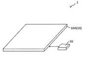
図1は、本技術の第1の実施の形態に係る表示装置1の斜視構成の一例を表す。表示装置1は、いわゆるLEDディスプレイと呼ばれるものであり、表示画素としてLEDが用いられたものである。表示装置1は、例えば、図1に示したように、表示パネル10と、表示パネル10(具体的には後述するセル10E)を制御する制御回路20とを備えている。<1. First Embodiment>
[Constitution]
FIG. 1 illustrates an example of a perspective configuration of the
(表示パネル10)
表示パネル10は、実装基板10Aと、対向基板10Bとを互いに重ね合わせたものである。対向基板10Bの表面が映像表示面となっており、中央部分に表示領域を有し、その周囲に、非表示領域であるフレーム領域を有している。対向基板10Bは、例えば、所定の間隙を介して、実装基板10Aと対向する位置に配置されている。なお、対向基板10Bが、実装基板10Aの上面に接していてもよい。対向基板10Bは、例えば、可視光を透過する光透過性の基板を有しており、例えば、ガラス基板、透明樹脂基板、または透明樹脂フィルムなどを有している。(Display panel 10)
The
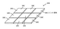
(実装基板10A)
図2は、実装基板10Aの斜視構成の一例を表す。実装基板10Aは、例えば、図2に示したように、タイル状に配置された複数のユニット基板10Cで構成されている。図3は、ユニット基板10Cの斜視構成の一例を表す。ユニット基板12Cは、例えば、タイル状に配置された複数のセル10Eと、各セル10Eを支持する支持基板10Dとを有している。各ユニット基板10Cは、さらに、制御基板(図示せず)を有している。制御基板は、例えば、後述の各電極パッド34を介して、各セル10Eと電気的に接続されている。支持基板10Dは、例えば、金属フレーム、もしくは、配線基板などで構成されている。支持基板10Dが配線基板で構成されている場合には、制御基板を兼ねることも可能である。このとき、支持基板10Dおよび制御基板の少なくとも一方が、各電極パッド34を介して、各セル10E(または後述の配線基板30)と電気的に接続されている。支持基板10Dが、本技術の「支持基板」の一具体例に相当する。電極パッド34が、本技術の「電極パッド」の一具体例に相当する。(Mounting
FIG. 2 illustrates an example of a perspective configuration of the mounting
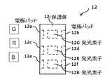
(セル10Eの回路構成)
図4は、セル10Eにおける回路構成の一例を表す。セル10Eは、上述の表示領域と対向する領域に、所定の方向(具体的には列方向)に延在する複数のデータ線Sigと、所定の方向(具体的には行方向)に延在する複数のゲート線Gateとを有している。データ線Sigおよびゲート線Gateは、例えば、銅によって形成されている。データ線Sigまたはゲート線Gateが、本技術の「第1配線」の一具体例に相当する。セル10Eは、さらに、上述の表示領域と対向する領域に、行列状に配置された複数の画素11を有している。各画素11は、発光素子12と、発光素子12を駆動する駆動IC13とを含んでいる。発光素子12が、本技術の「発光素子」の一具体例に相当する。駆動IC13が、本技術の「駆動回路」の一具体例に相当する。(Circuit configuration of
FIG. 4 illustrates an example of a circuit configuration in the
セル10Eは、さらに、上述の表示領域と対向する領域に、例えば、複数ののこぎり電圧線Sawと、複数の電源線VDD1,VDD2と、複数の参照電圧線Ref1,Ref2と、複数のグラウンド線GNDとを有している。各のこぎり電圧線Sawは、例えば、所定の方向(具体的には行方向)に延在している。各電源線VDD1、各電源線VDD2、各参照電圧線Ref1、各参照電圧線Ref2および各グラウンド線GNDは、それぞれ、例えば、所定の方向(具体的には列方向)に延在している。のこぎり電圧線Saw、電源線VDD1,VDD2、参照電圧線Ref1,Ref2およびグラウンド線GNDの少なくとも1つについては、駆動方式によっては省略され得る。のこぎり電圧線Saw、電源線VDD1,VDD2、参照電圧線Ref1,Ref2およびグラウンド線GNDは、例えば、銅によって形成されている。なお、以下では、データ線Sig、電源線VDD1、電源線VDD2、参照電圧線Ref1、参照電圧線Ref2およびグラウンド線GNDの総称として、列配線を用いる。また、以下では、ゲート線Gateおよびのこぎり電圧線Sawの総称として、行配線を用いる。 The
各データ線Sigは、映像信号に応じた信号が制御回路20によって入力される配線である。映像信号に応じた信号は、例えば、発光素子12の発光輝度を制御する信号である。複数のデータ線Sigは、例えば、発光素子12の発光色数に対応した種類の配線からなる。発光素子12が3色の発光色を有する場合には、複数のデータ線Sigは、例えば、複数のデータ線SigRと、複数のデータ線SigGと、複数のデータ線SigBとを含む。各データ線SigRは、赤色の映像信号に応じた信号が制御回路20によって入力される配線である。各データ線SigGは、緑色の映像信号に応じた信号が制御回路20によって入力される配線である。各データ線SigBは、青色の映像信号に応じた信号が制御回路20によって入力される配線である。 Each data line Sig is a wiring through which a signal corresponding to the video signal is input by the
発光素子12の発光色は、3色に限られず、4色以上であってもよい。複数のデータ線Sigが、複数のデータ線SigRと、複数のデータ線SigGと、複数のデータ線SigBとを含む場合には、1つのデータ線SigR、1つのデータ線SigGおよび1つのデータ線SigRからなる一組のデータ線Sigが、例えば、1画素列ごとに割り当てられる。駆動方式によっては、上記の一組のデータ線Sigは、複数画素列ごとに割り当てられる。また、駆動方式によっては、上記の一組のデータ線Sigは、単一のデータ線Sigに置き換えられ得る。 The light emission color of the
各ゲート線Gateは、発光素子12を選択する信号が制御回路20によって入力される配線である。発光素子12を選択する信号は、例えば、データ線Sigに入力された信号のサンプリングを開始するとともに、サンプリングされた信号を発光素子12に入力させ、発光素子12の発光を開始させる信号である。1つのゲート線Gateが、例えば、1画素行ごとに割り当てられる。各のこぎり電圧線Sawは、例えば、のこぎり状の波形を有する信号が制御回路20によって入力される配線である。のこぎり状の波形を有する信号は、サンプリングされた信号と対比され、例えば、のこぎり状の波形を有する信号の波高値が、サンプリングされた信号の波高値よりも高くなっている期間だけ、サンプリングされた信号が発光素子12に入力される。1つののこぎり電圧線Sawが、例えば、2画素行ごとに割り当てられる。各電源線VDD2は、発光素子12に対して供給する駆動電流が制御回路20によって入力される配線である。1つの電源線VDD2が、例えば、2画素列ごとに割り当てられる。各電源線VDD1、各参照電圧線Ref1、各参照電圧線Ref2および各グラウンド線GNDは、固定の電圧が制御回路20によって入力される配線である。各グラウンド線GNDには、グラウンド電位が入力される。1つの電源線VDD1が、例えば、2画素列ごとに割り当てられる。1つの参照電圧線Ref1が、例えば、2画素列ごとに割り当てられている。1つの参照電圧線Ref2が、例えば、2画素列ごとに割り当てられている。1つのグラウンド線GNDが、例えば、2画素列ごとに割り当てられる。 Each gate line Gate is a wiring through which a signal for selecting the
図5は、発光素子12の平面構成の一例を表す。図5において四角で囲まれた記号は、その記号に隣接する端子が後述の図6に記載の同一の記号に隣接する端子に電気的に接続されることを示している。発光素子12は、複数色の光を発するチップ状部品である。発光素子12の発光色が3色である場合、発光素子12は、例えば、赤色光を発する発光素子12R、緑色光を発する発光素子12Gおよび青色光を発する発光素子12Bを含んでいる。発光素子12R,12G,12Bは、例えば、樹脂などからなる保護体12iによって被覆されている。 FIG. 5 illustrates an example of a planar configuration of the
発光素子12R,12G,12Bは、例えば、LEDチップである。ここで、上記のLEDチップは、マイクロメータオーダーのチップサイズとなっており、例えば、数10μm角となっている。LEDチップは、例えば、導電型の互いに異なる半導体層で活性層を挟み込んだ積層構造を含む半導体層と、この半導体層の共通の面(同一面)に配置された2つの電極とを有している。発光素子12R,12G,12Bは、互いに別々のチップとなっていてもよいし、互いに共通の単一のチップとなっていてもよい。 The light emitting elements 12R, 12G, and 12B are, for example, LED chips. Here, the LED chip has a micrometer order chip size, for example, several tens of μm square. The LED chip has, for example, a semiconductor layer including a stacked structure in which an active layer is sandwiched between semiconductor layers having different conductivity types, and two electrodes disposed on a common surface (same surface) of the semiconductor layer. Yes. The light emitting elements 12R, 12G, and 12B may be separate chips, or may be a single chip that is common to each other.
発光素子12は、例えば、6つの電極パッド12a〜12fを有している。発光素子12Gにおいて、一方の電極は、電極パッド12aおよび配線16(図4参照)を介して駆動IC13の電極パッド13mと電気的に接続されており、他方の電極は、電極パッド12bおよび配線16を介してグラウンド線GNDと電気的に接続されている。発光素子12Rにおいて、一方の電極は、電極パッド12cおよび配線16を介して駆動IC13の電極パッド13oと電気的に接続されており、他方の電極は、電極パッド12dおよび配線16を介してグラウンド線GNDと電気的に接続されている。発光素子12Bにおいて、一方の電極は、電極パッド12eおよび配線16を介して駆動IC13の電極パッド13pと電気的に接続されており、他方の電極は、電極パッド12fおよび配線16を介してグラウンド線GNDと電気的に接続されている。 The
配線16は、例えば、画素11と、データ線Sig、ゲート線Gate、電源線VDD1、電源線VDD2、参照電圧線Ref1、参照電圧線Ref2、のこぎり電圧線Saw、またはグラウンド線GNDとを互いに電気的に接続する配線である。配線16は、例えば、画素11内において、発光素子12と、駆動IC13とを互いに電気的に接続する配線でもある。配線16は、例えば、スパッタリングやめっきによって形成されている。複数の配線16のうち一部の配線16は、画素11と、上記各種行配線や上記各種列配線とを互いに直接、接続している。複数の配線16のうち他の配線16は、断続的に形成された複数の部分配線からなっている。複数の部分配線からなる各配線16では、各部分電極は、例えば、後述の配線基板30の上面(例えば後述の配線層32E)に形成された1または複数の中継配線15を介して連結されている。中継配線15は、例えば、銅で形成されている。 For example, the
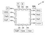
図6は、駆動IC13の平面構成の一例を表す。図6において四角で囲まれた配線名は、その配線名に隣接する端子に電気的に接続される配線の名称を示している。駆動IC13は、発光素子12の発光を制御する。駆動IC13は、例えば、14個の電極パッド13a,13b,13c,13d,13e,13f,13g,13h,13i,13k,13m,13n,13o,13pを有している。 FIG. 6 illustrates an example of a planar configuration of the
電極パッド13a,13b,13cは、配線16を介して、データ線SigG,SigR,SigBに電気的に接続されている。電極パッド13d,13eは、配線16を介して、電源線VDD1,VDD2に電気的に接続されている。電極パッド13f,13gは、配線16を介して、参照電位線Ref1,Ref2に電気的に接続されている。電極パッド13hは、配線16を介して、グラウンド線GNDに電気的に接続されている。電極パッド13iは、配線16を介して、ゲート線Gateに電気的に接続されている。電極パッド13kは、配線16を介して、のこぎり電圧線Sawに電気的に接続されている。電極パッド13m,13o,13nは、配線16を介して、発光素子12の電極パッド12a,12c,12eに電気的に接続されている。電極パッド13pは、配線16に接続されていない。 The
(セル10Eの構造)
図7は、セル10Eの断面構成の一例を表す。図7には、セル10Eにおいて、発光素子12、駆動IC13、データ線SigB1およびゲート線Gate2の形成されている箇所の断面構成の一例が示されている。図8は、セル10Eの配線レイアウトの一例を表す。図8には、2x2行列に対応する4つの画素11に接続された配線16等の配線レイアウトの一例が示されている。各セル10Eの配線レイアウトは、例えば、図8に記載のレイアウトが行方向および列方向に繰り返し配置されたレイアウトとなっている。図8において四角で囲まれた配線名は、その配線名に隣接するビア14(後述)に電気的に接続される配線の名称を示している。(Structure of
FIG. 7 illustrates an example of a cross-sectional configuration of the
セル10Eは、配線基板30と、配線基板30の上面に接して形成された微細L/S層40と、微細L/S層40の上面に行列状に配置された複数の画素11とを有している。配線基板30は、配線基板10Dとの関係では中間基板としての役割を有している。配線基板30は、本技術の「配線基板」の一具体例に相当する。微細L/S層40は、本技術の「微細L/S層」の一具体例に相当する。画素11が、本技術の「素子」の一具体例に相当する。 The
セル10Eは、さらに、例えば、各画素11を含む表面を被覆する埋め込み層44と、埋め込み層44に接して形成された遮光層45と、配線基板30の裏面に接して形成された絶縁層50とを有している。埋め込み層44は、可視光を透過する光透過性の材料で構成されている。遮光層45は、可視光を吸収する材料を含んで構成されている。絶縁層50は、例えば、紫外線硬化樹脂、または、熱硬化性樹脂で形成されている。 The
遮光層45は、各発光素子12と対向する箇所に開口45Aを有している。各発光素子12から発せられた光は各開口45Aを介して外部に出射される。絶縁層50は、セル10Eの外部接続端子としての各電極パッド34と対向する箇所に開口50Aを有している。従って、各電極パッド34は、開口50Aを介して、セル10E(配線基板30)の裏面に露出している。例えば、開口50A内に設けた金属バンプや半田バンプを介して、電極パッド34と配線基板10Dとが互いに電気的に接続されている。 The light shielding layer 45 has an opening 45 </ b> A at a location facing each light emitting
(配線基板30)
配線基板30は、例えば、層間の電気的な接続がビアでなされた積層基板である。配線基板30は、配線基板30の裏面に、外部接続端子としての複数の電極パッド34を有している。複数の電極パッド34は、例えば、データ線SigR1、データ線SigG1、データ線SigB1、ゲート線Gate1、ゲート線Gate2、電源線VDD1、参照電圧線Ref1、参照電圧線Ref2およびのこぎり電圧線Sawごとに、1つ以上設けられている。(Wiring board 30)
The
配線基板30は、微細L/S層40内で引き回された複数の配線16と、複数の電極パッド34とを電気的に接続する。配線基板30は、複数の配線16と、複数の電極パッド34とを電気的に接続する複数の貫通配線17を有している。各貫通配線17は、配線基板30を厚さ方向に貫通する配線である。ある貫通配線17は、ある層内で列方向に延在するデータ線Sigと、データ線Sigの上(または上方)に形成されると共に配線基板30の上面に露出する複数のビア14とを含んでいる。ある貫通配線17は、ある層内で行方向に延在するゲート線Gateと、ゲート線Gateの上(または上方)に形成されると共に配線基板30の上面に露出する複数のビア14とを含んでいる。 The
ある貫通配線17は、ある層内で列方向に延在する電源線VDD1と、電源線VDD1の上(または上方)に形成されると共に配線基板30の上面に露出する複数のビア14とを含んでいる。ある貫通配線17は、ある層内で列方向に延在する参照電圧線Ref1と、参照電圧線Ref1の上(または上方)に形成されると共に配線基板30の上面に露出する複数のビア14とを含んでいる。ある貫通配線17は、ある層内で列方向に延在する参照電圧線Ref2と、参照電圧線Ref2の上(または上方)に形成されると共に配線基板30の上面に露出する複数のビア14とを含んでいる。ある貫通配線17は、ある層内で列方向に延在するのこぎり電圧線Sawと、のこぎり電圧線Sawの上(または上方)に形成されると共に配線基板30の上面に露出する複数のビア14とを含んでいる。 A certain through
つまり、配線基板30において、複数のビア14は、データ線SigR1、データ線SigG1、データ線SigB1、ゲート線Gate1、ゲート線Gate2、電源線VDD1、参照電圧線Ref1、参照電圧線Ref2およびのこぎり電圧線Sawごとに、複数個ずつ設けられている。 That is, in the
ビア14は、絶縁層(例えば後述の絶縁層32D)の開口内に設けられている。ビア14は、絶縁層(例えば後述の絶縁層32D)の上面の配線(例えば配線16)と、絶縁層(例えば後述の絶縁層32D)の裏面の配線(例えばデータ線Sigやゲート線Gateなど)とを互いに電気的に接続する柱状配線である。ビア14は、例えば、コンフォーマルビア、または、フィルドビア(filled via)である。 The via 14 is provided in an opening of an insulating layer (for example, an insulating
複数のビア14は、複数の画素11の配列周期の整数倍の周期で配置されている。具体的には、データ線Sigの上(または上方)に形成された複数のビア14は、複数の画素11における、データ線Sigの延在方向(列方向)の配列周期の整数倍の周期で配置されている。同様に、ゲート線Gateの上(または上方)に形成された複数のビア14は、複数の画素11における、ゲート線Gateの延在方向(行方向)の配列周期の整数倍の周期で配置されている。電源線VDD1の上(または上方)に形成された複数のビア14は、複数の画素11における、電源線VDD1の延在方向(列方向)の配列周期の整数倍の周期で配置されている。参照電圧線Ref1の上(または上方)に形成された複数のビア14は、複数の画素11における、参照電圧線Ref1の延在方向(列方向)の配列周期の整数倍の周期で配置されている。参照電圧線Ref2の上(または上方)に形成された複数のビア14は、複数の画素11における、参照電圧線Ref2の延在方向(列方向)の配列周期の整数倍の周期で配置されている。のこぎり電圧線Sawの上(または上方)に形成された複数のビア14は、複数の画素11における、のこぎり電圧線Sawの延在方向(行方向)の配列周期の整数倍の周期で配置されている。 The plurality of
隣り合う複数の画素11が、1または複数の配線16を介して、共通の1つのビア14に電気的に接続されている。具体的には、データ線Sigの延在方向(列方向)に並んだ複数の画素11が、1または複数の配線16を介して、データ線Sigの上(または上方)に形成された共通の1つのビアに電気的に接続されている。同様に、ゲート線Gateの延在方向(行方向)に並んだ複数の画素11が、1または複数の配線16を介して、ゲート線Gateの上(または上方)に形成された共通の1つのビアに電気的に接続されている。電源線VDD1の延在方向(列方向)に並んだ複数の画素11が、1または複数の配線16を介して、電源線VDD1の上(または上方)に形成された共通の1つのビアに電気的に接続されている。参照電圧線Ref1の延在方向(列方向)に並んだ複数の画素11が、1または複数の配線16を介して、参照電圧線Ref1の上(または上方)に形成された共通の1つのビアに電気的に接続されている。参照電圧線Ref2の延在方向(列方向)に並んだ複数の画素11が、1または複数の配線16を介して、参照電圧線Ref2の上(または上方)に形成された共通の1つのビアに電気的に接続されている。のこぎり電圧線Sawの延在方向(行方向)に並んだ複数の画素11が、1または複数の配線16を介して、のこぎり電圧線Sawの上(または上方)に形成された共通の1つのビアに電気的に接続されている。 A plurality of
図8では、行方向に並んだ2つの画素11、列方向に並んだ2つの画素11、および2x2行列に対応する4つの画素11において、ビア14の共有化がなされている。例えば、列方向に並んだ2つの画素11が、1または複数の配線16を介して、データ線SigB1に電気的に接続された共通の1つのビア14に電気的に接続されている。このとき、データ線SigB1に電気的に接続された複数のビア14は、複数の画素11の列方向の配列周期の2倍の周期で配置されている。例えば、行方向に並んだ2つの画素11が、1または複数の配線16を介して、ゲート線Gate1に電気的に接続された共通の1つのビア14に電気的に接続されている。このとき、ゲート線Gate1に電気的に接続された複数のビア14は、複数の画素11の行方向の配列周期の2倍の周期で配置されている。例えば、2x2に対応する4つの画素11が、1または複数の配線16を介して、参照電圧線Ref1に電気的に接続された共通の1つのビア14に電気的に接続されている。このとき、参照電圧線Ref1に電気的に接続された複数のビア14は、複数の画素11の列方向の配列周期の2倍の周期で配置されている。 In FIG. 8, the via 14 is shared by the two
図8に記載の配線レイアウト(実施例の配線レイアウト)と、下記の比較例の配線レイアウトとを比較すると、2x2に対応する4つの画素11において必要となるビア14の数は、以下のようになる。なお、比較例では、各画素11において、データ線SigR1、データ線SigG1、データ線SigB1、ゲート線Gate1、ゲート線Gate2、電源線VDD1、参照電圧線Ref1、参照電圧線Ref2およびのこぎり電圧線Sawごとに、1つずつ、ビア14が設けられている。 When the wiring layout shown in FIG. 8 (the wiring layout of the embodiment) is compared with the wiring layout of the following comparative example, the number of
実施例 比較例
SigR1 2 2
SigG1 1 2
SigB1 1 2
SigR2 1 2
SigG2 1 2
SigB2 1 2
VDD1 1 4
Ref1 1 4
Ref2 1 4
Gate1 1 2
Gate2 1 2
Saw 2 4
合計 14 32Examples
Total 14 32
以上のことから、隣り合う複数の画素11でビア14を共有することにより、画素11ごとにビア14を設けた場合と比べて、1つの画素11あたりに必要となるビア14の数が少なくなることがわかる。 From the above, by sharing the
ところで、上述したように、各セル10Eの配線レイアウトは、例えば、図8に記載のレイアウトが行方向および列方向に繰り返し配置されたレイアウトとなっている。このとき、画素11のピッチは、各セル10E内だけでなく、隣接する2つのセル10E間においても、等ピッチとなっていることが好ましい。各セル10Eでは、各セル10Eの外部接続端子としての複数の電極パッド34が、セル10Eの裏面に設けられている。そのため、実装面の上面の外縁に外部接続端子を設けたときのような、画素11配置に使用できない額縁領域を省略したり、最小限にしたりすることができる。従って、各セル10Eから、そのような額縁領域が省略されているか、または、各セル10Eにおける、そのような額縁領域が最小限となっている場合には、隣接する2つのセル10E間においても、画素11のピッチを等ピッチにすることができる。 By the way, as described above, the wiring layout of each
配線基板30は、例えば、ビルドアップ基板であり、コア基板31と、コア基板31の上面に接して形成されたビルドアップ層32と、コア基板31の裏面に接して形成されたビルドアップ層33とを有している。配線基板30は、本技術の「ビルドアップ基板」の一具体例に相当する。ビルドアップ層32,33は、本技術の「ビルドアップ層」の一具体例に相当する。 The
コア基板31は、セル10Eの剛性の確保するものであり、例えば、ガラスエポキシ基板である。ビルドアップ層32は、1層以上の配線層を有している。ビルドアップ層32は、例えば、図7に示したように、配線層32A、絶縁層32B、配線層32C、絶縁層32Dおよび配線層32Eを、コア基板31の上面側からこの順に有している。ビルドアップ層33は、1層以上の配線層を有している。ビルドアップ層33は、例えば、図7に示したように、配線層33A、絶縁層33B、配線層33C、絶縁層33Dおよび配線層33Eを、コア基板31の裏面側からこの順に有している。配線層32A,32C,32E,33A,33C,33Eは、例えば、銅で形成されている。絶縁層32B,32D,33B,33Dは、例えば、紫外線硬化樹脂、または、熱硬化性樹脂で形成されている。 The
各データ線Sigは、例えば、配線層32Cに形成されている。図7には、データ線SigB1が、配線層32Cに形成されている様子が例示されている。各ゲート線Gateは、データ線Sigとは異なる層に形成されており、例えば、配線層32Aに形成されている。図7には、ゲート線Gate2が、配線層32Aに形成されている様子が例示されている。各電源線VDD2および各グラウンド線GNDは、例えば、配線層32Eに形成されている。各ビア14は、少なくともビルドアップ層32に形成されており、例えば、少なくとも絶縁層32Dと同一の層内に形成されている。図7には、各ビア14が、絶縁層32Dおよび配線層32Eと同一の層内に形成されている様子が例示されている。各電極パッド34は、ビルドアップ層33に形成されており、例えば、配線層33Eと同一の層内に形成されている。後述の中継配線15は、配線基板30の上面の配線層である配線層32Eに形成されている。 Each data line Sig is formed in the
(微細L/S層40)
微細L/S層40は、配線層42と、配線層42と配線基板30の上面との間に設けられた絶縁層41とを有している。絶縁層41は、配線層42と、配線基板30の上面とに接している。配線層42は、各配線16を含む層である。従って、絶縁層41は、各配線16と配線基板30の上面との間に設けられており、各配線16と、配線基板30の上面とに接している。絶縁層41は、各ビア14の上面と対向する位置に開口41Aを有している。絶縁層41は、ビア14と対向する位置ではなく、ビア14と電気的に接続された中継配線15と対向する位置に開口41Aを有していてもよい。絶縁層41は、さらに、上記部分電極と電気的に接続された中継配線15と対向する位置に開口41Aを有している。開口41Aの底面には、ビア14の一部、または、中継配線15の一部が露出している。絶縁層41は、例えば、VPAで形成されている。VPAは、レジストとして一般に使われるものであり、例えば、新日鉄化学社製のVPAが上市されている。絶縁層41がVPAで形成されている場合、例えば、VPAを選択的に露光・現像することによりVPAに開口41を形成することができる。(Fine L / S layer 40)
The fine L /
配線層42において、一部の配線16は、ビア14ごとに1本ずつ以上設けられており、別の配線16は、中間配線15ごとに1本ずつ以上設けられており、残りの配線16は、電源線VDD2およびグラウンド線GNDごとに複数本ずつ以上設けられている。配線層42(各配線16)は、例えば、開口41Aの底面および側面を含む配線基板30の上面に接するシード層42Aと、シード層42Aの上面に接するめっき層42Bとを有している。シード層42Aは、製造過程においてめっき層42Bをめっきで形成する際のめっき成長面となる。シード層42Aは、開口41Aの底面と接しており、ビア14および中継配線15と電気的に接続されている。シード層42Aは、例えば、銅で形成されている。めっき層42Bは、製造過程においてシード層42Aをめっき成長面としてめっき処理により形成されたものである。なお、配線層42(各配線16)は、例えば、スパッタリングにより形成された層であってもよい。 In the
上述したように、配線層42(各配線16)は、絶縁層41の上面に接して形成されている。一方、各画素11の電極は、シード層42Aの上面に接して形成されている。そのため、発光素子12および駆動IC13は、互いに同一の面(シード層42Aの上面)上に形成されているが、厳密には、配線層42(各配線16)の形成面(絶縁層41の上面)とは別の面に形成されている。しかし、各画素11の実装という観点からは、絶縁層41の上面とシード層42Aの上面とを含む面が実装面41Sとなっていると言える。従って、配線層42(各配線16)は、各画素11の実装面41Sに形成されており、かつ、各画素11と実質的に共通の面に形成されている。 As described above, the wiring layer 42 (each wiring 16) is formed in contact with the upper surface of the insulating
配線層42(各配線16)は、例えば、ビア14、ビア14と電気的に接続された部材(例えば中継配線15)、および、上記部分電極と電気的に接続された中継配線15とめっき接合されている。配線層42(各配線16)をめっきにより形成する際に、配線層42(各配線16)と、ビア14等との接合が、配線層42(各配線16)の形成プロセスの中で一括して行われてもよい。配線層42(各配線16)は、例えば、画素11(発光素子12および駆動IC13)とめっき接合されている。配線層42(各配線16)をめっきにより形成する際に、配線層42(各配線16)と、画素11との接合が、配線層42(各配線16)の形成プロセスの中で一括して行われてもよい。 The wiring layer 42 (each wiring 16) includes, for example, a via 14 and a member (for example, the relay wiring 15) electrically connected to the via 14 and the
微細L/S層40のL/S(line and space)は、配線基板30のL/Sよりも小さくなっている。L/Sとは、面内で最も狭い配線ピッチを指している。微細L/S層40のL/Sは、複数の信号線Sig、複数のゲート線Gate、複数の電圧線VDD1、複数の参照電圧線Ref1、複数の参照電圧線Ref2、およびのこぎり電圧線SawのL/Sよりも小さくなっている。微細L/S層40のL/Sは、例えば、25μm程度である。一方、配線基板30のL/Sは、例えば、75μm程度である。 The L / S (line and space) of the fine L /
[製造方法]
次に、図9〜図13を参照しつつ、セル10Eの製造方法の一例について説明する。図9〜図13は、セル10Eの製造過程の一例を工程順に表す。[Production method]
Next, an example of a method for manufacturing the
まず、配線基板30を用意する。次に、配線基板30の上面に絶縁層41を形成したのち、所定の方法で、絶縁層41のうち、ビア14の上面と対向する位置に開口41Aを形成する(図9)。このとき、図示しないが、所定の方法で、ビア14や上記部分配線と電気的に接続された中継配線15の上面と対向する位置にも開口41Aを形成する。次に、開口41Aの底面および側面を含む配線基板30の上面にシード層42Aを形成する(図10)。 First, the
次に、表面全体に絶縁性の接着剤を塗布するなどして、発光素子12や駆動IC13を仮固定するための固定層43Aを形成する(図11参照)。接着剤の代わりに、シリコーン系やアクリル系で代表されるような粘着剤の層を固定層43Aとして形成してもよい。続いて、発光素子12や駆動IC13を固定層43Aによって仮固定する(図11)。このとき、発光素子12の電極パッド12a〜12eや、駆動IC13の電極パッド13a〜13pを、後述のめっき処理において成長する金属体(めっき層42B)と接続可能となる程度に近づけて配置する。 Next, a
次に、発光素子12や駆動IC13を仮固定している部分(固定層43Aのうち、発光素子12や駆動IC13の底面に存在する部分)以外の固定層43Aを除去する。その結果、発光素子12や駆動IC13の底面だけに固定層43Aが残る(図12)。図12では、残った固定層43Aを固定層43と記載した。固定層43Aの除去に際して、例えば、ドライエッチングや有機溶剤浸漬等を行うことができる。なお、あらかじめ、発光素子12や駆動IC13を仮固定する場所にだけ、絶縁性の接着剤を塗布しておいてもよい。 Next, the fixed
次に、シード層42Aをめっき成長面としてめっき処理を行い、シード層42Aの上面にめっき層42Bを形成する(図13)。これにより、配線層42(各配線16)が形成される。このとき、配線層42(各配線16)と、ビア14等との接合が、配線層42(各配線16)の形成プロセスの中で一括して行われる。また、配線層42(各配線16)と、画素11との接合が、配線層42(各配線16)の形成プロセスの中で一括して行われる。その後は、発光素子12や駆動IC13を埋め込み層43で埋め込んだ後に、遮光層45を形成する(図7参照)。このようにして、セル10Eが製造される。 Next, a plating process is performed using the
[作用・効果]
次に、表示装置1の作用、効果について説明する。本実施の形態では、配線基板30において、層内で所定の方向に延在する配線(例えば、データ線Sig、ゲート線Gate)ごとに複数のビア14が設けられている。層内で所定の方向に延在する配線ごとに設けられた複数のビア14が、複数の画素11の配列周期の整数倍の周期で配置されている。そして、微細L/S層40上で隣り合う複数の画素11が、微細L/S層40内の1または複数の配線16を介して、共通のビア14に電気的に接続されている。このように、隣り合う複数の画素11でビア14を共有することにより、画素11ごとにビア14を設けた場合と比べて、1つの画素11あたりに必要となるビア14の数が少なくなる。その結果、配線基板30上の微細L/S層40のL/Sを、配線基板30内の複数の配線(例えば、複数のデータ線Sig、または、複数のゲート線Gate)のL/Sよりも小さくした場合に、配線基板30上の配線層42の数を1つとすることができる。従って、本実施の形態では、配線基板30上の配線層42を多層にすることなく、実装面41Sの配線ピッチを狭くすることができる。[Action / Effect]
Next, the operation and effect of the
<2.変形例>
[変形例1]
上記実施の形態において、例えば、図14に示したように、画素11が、発光素子12および駆動IC13を一体に形成したものであってもよい。<2. Modification>
[Modification 1]
In the above embodiment, for example, as shown in FIG. 14, the
[変形例2]
上記実施の形態およびその変形例において、発光素子12の発光色が単一であってもよい。この場合に、セル10Eが、例えば、開口45A内に、複数色のカラーフィルタを有していてもよい。また、上記変形例2において、発光素子12の発光色が単一であってもよい。この場合に、対向基板10Bが、例えば、開口45A内に、複数色のカラーフィルタを有していてもよい。[Modification 2]
In the above embodiment and its modifications, the
<3.第2の実施の形態>
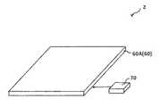
図15は、本技術の第2の実施の形態に係る照明装置2の斜視構成の一例を表す。照明装置2は、上記第1の実施の形態の表示装置1およびその変形例(変形例1,2)において、データ線Sigに入力される信号が、映像信号のような時々刻々、変化するものではなく、照明光の明るさに応じた固定値となっているものに相当する。照明装置2は、例えば、図15に示したように、照明パネル60と、照明パネル60を制御する制御回路70とを備えている。<3. Second Embodiment>
FIG. 15 illustrates an example of a perspective configuration of the
照明パネル60は、実装基板60Aと、対向基板60Bとを互いに重ね合わせたものである。対向基板60Bの表面が光出射面となっている。対向基板60Bは、所定の間隙を介して、実装基板60Aと対向する位置に配置されている。対向基板60Bは、例えば、可視光を透過する光透過性の基板を有しており、例えば、ガラス基板、または透明樹脂基板などを有している。 The
実装基板60Aは、例えば、図2と同様に、タイル状に配置された複数のユニット基板で構成されている。ユニット基板は、例えば、タイル状に配置された複数のセルと、各セルを支持する配線基板とを有している。各セルでは、例えば、図4、図7、図8、図14において、データ線Sigに入力される信号が、照明光の明るさに応じた固定値となっている場合に、画素11の駆動にとって必要のない配線が、適宜、省略される。 For example, the mounting
[作用・効果]
次に、照明装置2の作用、効果について説明する。本実施の形態では、上記第1の実施の形態およびその変形例に係る表示装置1と同様に、配線基板30において、層内で所定の方向に延在する配線ごとに複数のビア14が設けられている。層内で所定の方向に延在する配線ごとに設けられた複数のビア14が、複数の画素11の配列周期の整数倍の周期で配置されている。そして、微細L/S層40上で隣り合う複数の受光素子が、微細L/S層40内の1または複数の配線16を介して、共通のビア14に電気的に接続されている。このように、隣り合う複数の画素11でビア14を共有することにより、画素11ごとにビア14を設けた場合と比べて、1つの画素11あたりに必要となるビア14の数が少なくなる。その結果、配線基板30上の微細L/S層40のL/Sを、配線基板30内の複数の配線のL/Sよりも小さくした場合に、配線基板30上の配線層42の数を1つとすることができる。従って、本実施の形態では、配線基板30上の配線層42を多層にすることなく、実装面41Sの配線ピッチを狭くすることができる。[Action / Effect]
Next, functions and effects of the
<4.第3の実施の形態>
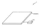
図16は、本技術の第3の実施の形態に係る受光装置3の斜視構成の一例を表す。受光装置3は、上記第1の実施の形態の表示装置1において、画素11の代わりに受光素子を設けたものに相当する。受光装置2は、例えば、図16に示したように、受光パネル80と、受光パネル80を制御する制御回路90とを備えている。<4. Third Embodiment>
FIG. 16 illustrates an example of a perspective configuration of the
受光パネル80は、実装基板80Aと、対向基板80Bとを互いに重ね合わせたものである。対向基板80Bの表面が受光面となっている。対向基板80Bは、所定の間隙を介して、実装基板80Aと対向する位置に配置されている。対向基板80Bは、例えば、可視光を透過する光透過性の基板を有しており、例えば、ガラス基板、または透明樹脂基板などを有している。 The
実装基板80Aは、例えば、図2と同様に、タイル状に配置された複数のユニット基板で構成されている。ユニット基板は、例えば、タイル状に配置された複数のセルと、各セルを支持する配線基板とを有している。各セルは、例えば、図4、図7、図14において、画素11の代わりに受光素子を設けたものに相当する。ただし、受光素子の駆動にとって必要のない配線は、適宜、省略される。 The mounting
[作用・効果]
次に、受光装置3の作用、効果について説明する。本実施の形態では、上記第1の実施の形態およびその変形例に係る表示装置1と同様に、配線基板30において、層内で所定の方向に延在する配線ごとに複数のビア14が設けられている。層内で所定の方向に延在する配線ごとに設けられた複数のビア14が、複数の受光素子の配列周期の整数倍の周期で配置されている。そして、微細L/S層40上で隣り合う複数の受光素子が、微細L/S層40内の1または複数の配線16を介して、共通のビア14に電気的に接続されている。このように、隣り合う複数の受光素子でビア14を共有することにより、受光素子ごとにビア14を設けた場合と比べて、1つの画素11あたりに必要となるビア14の数が少なくなる。その結果、配線基板30上の微細L/S層40のL/Sを、配線基板30内の複数の配線のL/Sよりも小さくした場合に、配線基板30上の配線層42の数を1つとすることができる。従って、本実施の形態では、配線基板30上の配線層42を多層にすることなく、実装面41Sの配線ピッチを狭くすることができる。[Action / Effect]
Next, functions and effects of the
<5.各実施の形態に共通の変形例>
上記各実施の形態およびその変形例において、遮光層45が対向基板10B,60B,80Bの裏面(実装基板10A,60A,80A側の表面)に配置されていてもよい。<5. Modification common to each embodiment>
In each of the above embodiments and modifications thereof, the light shielding layer 45 may be disposed on the back surface of the
上記各実施の形態およびその変形例において、例えば、図17〜図19に示したように、対向基板10B,60B,80Bが省略されていてもよい。また、上記各実施の形態およびその変形例において、対向基板10B,60B,80Bが、ユニット基板10Cごとに、またはセル12Eごとに1つずつ設けられていてもよい。 In each of the above-described embodiments and modifications thereof, for example, as illustrated in FIGS. 17 to 19, the
上記各実施の形態およびその変形例において、遮光層45が省略されていてもよい。 In each of the above embodiments and modifications thereof, the light shielding layer 45 may be omitted.
また、上記各実施の形態およびその変形例では、各画素11(発光素子12および駆動IC13)が、配線層42(各配線16)とめっき接合されていたが、例えば、半田接合されていてもよい。例えば、発光素子12および駆動IC13の電極パッドに半田バンプを設けた上で、発光素子12および駆動IC13を、各配線16上に配置したのち、リフローを行う。これにより、発光素子12および駆動IC13を、各配線16に半田接合することができる。なお、本明細書中に記載された効果はあくまで例示であって限定されるものではなく、また、他の効果があってもよい。 Further, in each of the above embodiments and modifications thereof, each pixel 11 (
また、例えば、本技術は以下のような構成を取ることができる。
(1)
配線基板と、
前記配線基板の上面に接して形成された微細L/S(line and space)層と、
前記微細L/S層の上面に行列状に配置された複数の素子と
を備え、
前記配線基板は、
層内で所定の方向に延在する複数の第1配線と、
前記第1配線ごとに複数設けられ、かつ複数の前記素子の配列周期の整数倍の周期で配置された複数のビアと
を有し、
前記微細L/S層は、
前記ビアごとに1つ以上設けられた複数の第2配線と、
各前記第2配線と、前記配線基板の上面との間に設けられ、各前記第2配線と、前記配線基板の上面とに接する絶縁層と
を有し、
前記微細L/S層のL/Sは、複数の前記第1配線のL/Sよりも小さくなっており、
隣り合う複数の前記素子が、1または複数の前記第2配線を介して、共通の前記ビアに電気的に接続されている
実装基板。
(2)
複数の前記第1配線は、行方向または列方向に延在し、
複数の前記ビアは、複数の前記素子における、前記第1配線の延在方向の配列周期の整数倍の周期で配置され、
前記第1配線の延在方向に並んだ複数の前記素子が、1または複数の前記第2配線を介して、共通の前記ビアに電気的に接続されている
(1)に記載の実装基板。
(3)
各前記ビアは、前記第2配線の上または上方に形成されると共に前記配線基板の上面に露出している
(1)または(2)に記載の実装基板。
(4)
前記配線基板は、前記第1配線ごとに1つ以上設けられ、前記配線基板の裏面に露出する複数の電極パッドを有する
(1)ないし(3)のいずれか1つに記載の実装基板。
(5)
前記第2配線は、前記ビアまたは前記ビアと電気的に接続された部材とめっき接合されており、さらに、各前記素子とめっき接合されている
(1)ないし(4)のいずれか1つに記載の実装基板。
(6)
前記配線基板は、コア基板と、前記コア基板の両面にそれぞれ1層以上形成されたビルドアップ層とを有するビルドアップ基板であり、
各前記ビアは、少なくとも前記配線基板の上面側の前記ビルドアップ層に形成され、
各前記電極パッドは、前記配線基板の裏面側の前記ビルドアップ層に形成されている
(1)ないし(5)のいずれか1つに記載の実装基板。
(7)
各前記素子は、発光素子と、前記発光素子を駆動する駆動回路とを含む
(1)ないし(6)のいずれか1つに記載の実装基板。
(8)
1または複数の実装基板と、
1または複数の前記実装基板を制御する制御回路と
を備え、
前記実装基板は、
配線基板と、
前記配線基板の上面に接して形成された微細L/S(line and space)層と、
前記微細L/S層の上面に行列状に配置された複数の素子と
を有し、
前記配線基板は、
層内で所定の方向に延在する複数の第1配線と、
前記第1配線ごとに複数設けられ、かつ複数の前記素子の配列周期の整数倍の周期で配置された複数のビアと
を有し、
前記微細L/S層は、
前記ビアごとに1つ以上設けられた複数の第2配線と、
各前記第2配線と、前記配線基板の上面との間に設けられ、各前記第2配線と、前記配線基板の上面とに接する絶縁層と
を有し、
前記微細L/S層のL/S(line and space)は、複数の前記第1配線のL/Sよりも小さくなっており、
隣り合う複数の前記素子が、1または複数の前記第2配線を介して、共通の前記ビアに電気的に接続されている
電子機器。
(9)
当該電子機器は、
複数の前記実装基板を支持する支持基板と、
複数の前記実装基板を制御する制御基板と
をさらに備え、
複数の前記実装基板は、前記支持基板上にタイル状に配置され、
各前記配線基板は、前記第1配線ごとに1つ以上設けられ、前記第1配線と電気的に接続されると共に、前記配線基板の裏面に露出する複数の電極パッドを有し、
前記支持基板および前記制御基板の少なくとも一方は、各前記電極パッドを介して、各前記配線基板と電気的に接続されている
(8)に記載の電子機器。For example, this technique can take the following composition.
(1)
A wiring board;
A fine L / S (line and space) layer formed in contact with the upper surface of the wiring board;
A plurality of elements arranged in a matrix on the upper surface of the fine L / S layer,
The wiring board is
A plurality of first wires extending in a predetermined direction within the layer;
A plurality of vias provided for each of the first wirings and arranged with a period that is an integral multiple of the array period of the plurality of elements;
The fine L / S layer is
A plurality of second wirings provided at least one for each via;
An insulating layer provided between each of the second wirings and the upper surface of the wiring board and in contact with each of the second wirings and the upper surface of the wiring board;
L / S of the fine L / S layer is smaller than L / S of the plurality of first wirings,
A plurality of adjacent elements are electrically connected to the common via via one or more second wirings.
(2)
The plurality of first wirings extend in a row direction or a column direction,
The plurality of vias are arranged at a cycle that is an integral multiple of the arrangement cycle in the extending direction of the first wiring in the plurality of elements.
The mounting substrate according to (1), wherein the plurality of elements arranged in the extending direction of the first wiring are electrically connected to the common via via one or more second wirings.
(3)
Each of the vias is formed on or above the second wiring and is exposed on an upper surface of the wiring board. (1) or (2).
(4)
One or more said wiring boards are provided for every said 1st wiring, and have a several electrode pad exposed to the back surface of the said wiring board. The mounting board | substrate as described in any one of (1) thru | or (3).
(5)
The second wiring is plated and bonded to the via or a member electrically connected to the via, and is further plated and bonded to each of the elements (1) to (4) The mounting board described.
(6)
The wiring board is a build-up board having a core board and a build-up layer formed on each of both surfaces of the core board.
Each of the vias is formed in at least the build-up layer on the upper surface side of the wiring board,
Each said electrode pad is formed in the said buildup layer of the back surface side of the said wiring board. The mounting board | substrate as described in any one of (1) thru | or (5).
(7)
Each said element contains a light emitting element and the drive circuit which drives the said light emitting element. The mounting board | substrate as described in any one of (1) thru | or (6).
(8)
One or more mounting boards;
A control circuit for controlling one or a plurality of the mounting boards,
The mounting substrate is
A wiring board;
A fine L / S (line and space) layer formed in contact with the upper surface of the wiring board;
A plurality of elements arranged in a matrix on the upper surface of the fine L / S layer,
The wiring board is
A plurality of first wires extending in a predetermined direction within the layer;
A plurality of vias provided for each of the first wirings and arranged with a period that is an integral multiple of the array period of the plurality of elements;
The fine L / S layer is
A plurality of second wirings provided at least one for each via;
An insulating layer provided between each of the second wirings and the upper surface of the wiring board and in contact with each of the second wirings and the upper surface of the wiring board;
L / S (line and space) of the fine L / S layer is smaller than L / S of the plurality of first wirings,
An electronic apparatus in which a plurality of adjacent elements are electrically connected to the common via via one or more second wirings.
(9)
The electronic device
A support substrate for supporting a plurality of the mounting substrates;
A control board for controlling a plurality of the mounting boards,
The plurality of mounting substrates are arranged in a tile shape on the support substrate,
Each of the wiring boards is provided with one or more for each of the first wirings, and has a plurality of electrode pads that are electrically connected to the first wiring and exposed on the back surface of the wiring board;
The electronic device according to (8), wherein at least one of the support substrate and the control substrate is electrically connected to each wiring substrate via each electrode pad.
1…表示装置、10…表示パネル、10A…実装基板、10B…対向基板、10C…ユニット基板、10D…配線基板、10E…セル、11…画素、12,12B,12G,12R…発光素子、12a,12b,12c,12d,12e,12f,13a,13b,13c,13d,13e,13f,13g,13h,13i,13k,13m,13n,13o,13p…電極パッド、12i…保護体、13…駆動IC、15…中継配線、16…配線、17…貫通配線、20…制御回路、30…配線基板、31…コア基板、32,33…ビルドアップ基板、32A,32C,32E,33A,33C,33E…配線層、32B,32D,33B,33D…絶縁層、34…電極パッド、40…微細L/S層、41…絶縁層、41A…開口、41S…実装面、42…配線層、42A…シード層、42B…めっき層、43,43A…固定層、44…埋め込み層、45…遮光層、45A…開口、50…絶縁層、50A…開口、Gate,Gate1,Gate2…ゲート線、GND…グラウンド線、Ref1,Ref2…参照電圧線、Saw…のこぎり電圧線、Sig,SigB,SigB1,SigB2,SigG,SigG1,SigG2,SigR,SigR1,SigR2…データ線、VDD1,VDD2…電源線。 DESCRIPTION OF
Claims (9)
Translated fromJapanese前記配線基板の上面に接して形成された微細L/S(line and space)層と、
前記微細L/S層の上面に行列状に配置された複数の素子と
を備え、
前記配線基板は、
層内で所定の方向に延在する複数の第1配線と、
前記第1配線ごとに複数設けられ、かつ複数の前記素子の配列周期の整数倍の周期で配置された複数のビアと
を有し、
前記微細L/S層は、
前記ビアごとに1つ以上設けられた複数の第2配線と、
各前記第2配線と、前記配線基板の上面との間に設けられ、各前記第2配線と、前記配線基板の上面とに接する絶縁層と
を有し、
前記微細L/S層のL/Sは、複数の前記第1配線のL/Sよりも小さくなっており、
隣り合う複数の前記素子が、1または複数の前記第2配線を介して、共通の前記ビアに電気的に接続されている
実装基板。A wiring board;
A fine L / S (line and space) layer formed in contact with the upper surface of the wiring board;
A plurality of elements arranged in a matrix on the upper surface of the fine L / S layer,
The wiring board is
A plurality of first wires extending in a predetermined direction within the layer;
A plurality of vias provided for each of the first wirings and arranged with a period that is an integral multiple of the array period of the plurality of elements;
The fine L / S layer is
A plurality of second wirings provided at least one for each via;
An insulating layer provided between each of the second wirings and the upper surface of the wiring board and in contact with each of the second wirings and the upper surface of the wiring board;
L / S of the fine L / S layer is smaller than L / S of the plurality of first wirings,
A plurality of adjacent elements are electrically connected to the common via via one or more second wirings.
複数の前記ビアは、複数の前記素子における、前記第1配線の延在方向の配列周期の整数倍の周期で配置され、
前記第1配線の延在方向に並んだ複数の前記素子が、1または複数の前記第2配線を介して、共通の前記ビアに電気的に接続されている
請求項1に記載の実装基板。The plurality of first wirings extend in a row direction or a column direction,
The plurality of vias are arranged at a cycle that is an integral multiple of the arrangement cycle in the extending direction of the first wiring in the plurality of elements.
The mounting substrate according to claim 1, wherein the plurality of elements arranged in the extending direction of the first wiring are electrically connected to the common via via the one or more second wirings.
請求項2に記載の実装基板。The mounting board according to claim 2, wherein each of the vias is formed on or above thefirst wiring and is exposed on an upper surface of the wiring board.
請求項3に記載の実装基板。The mounting substrate according to claim 3, wherein one or more wiring boards are provided for each of the first wirings and have a plurality of electrode pads exposed on a back surface of the wiring board.
請求項4に記載の実装基板。The mounting substrate according to claim 4, wherein the second wiring is plated and bonded to the via or a member electrically connected to the via, and is further plated and bonded to each of the elements.
各前記ビアは、少なくとも前記配線基板の上面側の前記ビルドアップ層に形成され、
各前記電極パッドは、前記配線基板の裏面側の前記ビルドアップ層に形成されている
請求項5に記載の実装基板。The wiring board is a build-up board having a core board and a build-up layer formed on each of both surfaces of the core board.
Each of the vias is formed in at least the build-up layer on the upper surface side of the wiring board,
The mounting board according to claim 5, wherein each of the electrode pads is formed on the build-up layer on the back side of the wiring board.
請求項5に記載の実装基板。The mounting board according to claim 5, wherein each of the elements includes a light emitting element and a drive circuit that drives the light emitting element.
1または複数の前記実装基板を制御する制御回路と
を備え、
前記実装基板は、
配線基板と、
前記配線基板の上面に接して形成された微細L/S(line and space)層と、
前記微細L/S層の上面に行列状に配置された複数の素子と
を有し、
前記配線基板は、
層内で所定の方向に延在する複数の第1配線と、
前記第1配線ごとに複数設けられ、かつ複数の前記素子の配列周期の整数倍の周期で配置された複数のビアと
を有し、
前記微細L/S層は、
前記ビアごとに1つ以上設けられた複数の第2配線と、
各前記第2配線と、前記配線基板の上面との間に設けられ、各前記第2配線と、前記配線基板の上面とに接する絶縁層と
を有し、
前記微細L/S層のL/S(line and space)は、複数の前記第1配線のL/Sよりも小さくなっており、
隣り合う複数の前記素子が、1または複数の前記第2配線を介して、共通の前記ビアに電気的に接続されている
電子機器。One or more mounting boards;
A control circuit for controlling one or a plurality of the mounting boards,
The mounting substrate is
A wiring board;
A fine L / S (line and space) layer formed in contact with the upper surface of the wiring board;
A plurality of elements arranged in a matrix on the upper surface of the fine L / S layer,
The wiring board is
A plurality of first wires extending in a predetermined direction within the layer;
A plurality of vias provided for each of the first wirings and arranged with a period that is an integral multiple of the array period of the plurality of elements;
The fine L / S layer is
A plurality of second wirings provided at least one for each via;
An insulating layer provided between each of the second wirings and the upper surface of the wiring board and in contact with each of the second wirings and the upper surface of the wiring board;
L / S (line and space) of the fine L / S layer is smaller than L / S of the plurality of first wirings,
An electronic apparatus in which a plurality of adjacent elements are electrically connected to the common via via one or more second wirings.
複数の前記実装基板を支持する支持基板と、
複数の前記実装基板を制御する制御基板と
をさらに備え、
複数の前記実装基板は、前記支持基板上にタイル状に配置され、
各前記配線基板は、前記第1配線ごとに1つ以上設けられ、前記第1配線と電気的に接続されると共に、前記配線基板の裏面に露出する複数の電極パッドを有し、
前記支持基板および前記制御基板の少なくとも一方は、各前記電極パッドを介して、各前記配線基板と電気的に接続されている
請求項8に記載の電子機器。
The electronic device
A support substrate for supporting a plurality of the mounting substrates;
A control board for controlling a plurality of the mounting boards,
The plurality of mounting substrates are arranged in a tile shape on the support substrate,
Each of the wiring boards is provided with one or more for each of the first wirings, and has a plurality of electrode pads that are electrically connected to the first wiring and exposed on the back surface of the wiring board;
The electronic device according to claim 8, wherein at least one of the support substrate and the control substrate is electrically connected to each wiring substrate via each electrode pad.
Priority Applications (6)
| Application Number | Priority Date | Filing Date | Title |
|---|---|---|---|
| JP2014074844AJP6128046B2 (en) | 2014-03-31 | 2014-03-31 | Mounting board and electronic equipment |
| US15/128,443US11139248B2 (en) | 2014-03-31 | 2015-03-17 | Mounting substrate and electronic apparatus |
| EP15773964.0AEP3128504B1 (en) | 2014-03-31 | 2015-03-17 | Mounting substrate and electronic device |
| PCT/JP2015/057847WO2015151796A1 (en) | 2014-03-31 | 2015-03-17 | Mounting substrate and electronic device |
| CN201580015737.3ACN106133814B (en) | 2014-03-31 | 2015-03-17 | Mounting substrates and electronic devices |
| CN201910145904.6ACN110060978B (en) | 2014-03-31 | 2015-03-17 | Install the substrate and electronics |
Applications Claiming Priority (1)
| Application Number | Priority Date | Filing Date | Title |
|---|---|---|---|
| JP2014074844AJP6128046B2 (en) | 2014-03-31 | 2014-03-31 | Mounting board and electronic equipment |
Related Child Applications (1)
| Application Number | Title | Priority Date | Filing Date |
|---|---|---|---|
| JP2017080090ADivisionJP6527194B2 (en) | 2017-04-13 | 2017-04-13 | Display device |
Publications (2)
| Publication Number | Publication Date |
|---|---|
| JP2015198145A JP2015198145A (en) | 2015-11-09 |
| JP6128046B2true JP6128046B2 (en) | 2017-05-17 |
Family
ID=54240128
Family Applications (1)
| Application Number | Title | Priority Date | Filing Date |
|---|---|---|---|
| JP2014074844AActiveJP6128046B2 (en) | 2014-03-31 | 2014-03-31 | Mounting board and electronic equipment |
Country Status (5)
| Country | Link |
|---|---|
| US (1) | US11139248B2 (en) |
| EP (1) | EP3128504B1 (en) |
| JP (1) | JP6128046B2 (en) |
| CN (2) | CN110060978B (en) |
| WO (1) | WO2015151796A1 (en) |
Families Citing this family (19)
| Publication number | Priority date | Publication date | Assignee | Title |
|---|---|---|---|---|
| JP2015197544A (en) | 2014-03-31 | 2015-11-09 | ソニー株式会社 | Mounting board and electronic apparatus |
| JP2015197543A (en) | 2014-03-31 | 2015-11-09 | ソニー株式会社 | Mounting board and electronic equipment |
| JP2017009725A (en)* | 2015-06-19 | 2017-01-12 | ソニー株式会社 | Display device |
| CN104979326B (en)* | 2015-07-09 | 2017-12-05 | 深圳市晶泓科技有限公司 | LED luminescence components, LED luminescent panels and LED display |
| WO2018074611A1 (en)* | 2016-10-19 | 2018-04-26 | 株式会社オルガノサーキット | Active matrix led display |
| CN106773415A (en)* | 2017-01-16 | 2017-05-31 | 京东方科技集团股份有限公司 | A kind of array base palte, display panel and display device |
| JP6781087B2 (en)* | 2017-02-28 | 2020-11-04 | 京セラ株式会社 | Display device |
| JP6527194B2 (en)* | 2017-04-13 | 2019-06-05 | ソニーセミコンダクタソリューションズ株式会社 | Display device |
| JP7173653B2 (en)* | 2017-06-27 | 2022-11-16 | ソニーグループ株式会社 | Display element mounting board and display device |
| JP7267683B2 (en)* | 2018-04-25 | 2023-05-02 | シャープ株式会社 | Light-emitting element module |
| US10593852B2 (en)* | 2018-06-20 | 2020-03-17 | Innolux Corporation | Display device having a plurality of main pads, a plurality of redundant pads, and a light-emitting device |
| KR102182584B1 (en)* | 2019-03-20 | 2020-11-24 | 주식회사 테토스 | LED display module |
| JP6883874B2 (en)* | 2019-05-31 | 2021-06-09 | エイテックス株式会社 | Printed circuit board for surface light emitting device and surface light emitting device |
| US11508704B2 (en)* | 2019-12-17 | 2022-11-22 | Seoul Viosys Co., Ltd. | Method of repairing light emitting device and display panel having repaired light emitting device |
| US11476301B2 (en)* | 2020-01-14 | 2022-10-18 | Au Optronics Corporation | Display apparatus and manufacturing method thereof |
| CN114280841B (en)* | 2020-09-27 | 2023-06-20 | 合肥鑫晟光电科技有限公司 | Light-emitting substrate and display device |
| JP7368338B2 (en)* | 2020-10-07 | 2023-10-24 | エルジー ディスプレイ カンパニー リミテッド | Micro LED display device |
| JP7618830B2 (en)* | 2021-09-09 | 2025-01-21 | 京セラ株式会社 | Display device and multi-display |
| CN114999339B (en)* | 2022-05-30 | 2023-12-05 | 安徽精卓光显技术有限责任公司 | Display panel, display screen and electronic equipment |
Family Cites Families (55)
| Publication number | Priority date | Publication date | Assignee | Title |
|---|---|---|---|---|
| US5812105A (en) | 1996-06-10 | 1998-09-22 | Cree Research, Inc. | Led dot matrix drive method and apparatus |
| CA2241555C (en) | 1995-12-29 | 2006-07-11 | Cree Research, Inc. | True color flat panel display using an led dot matrix and led dot matrix drive method and apparatus |
| JP3560756B2 (en) | 1997-02-13 | 2004-09-02 | アルプス電気株式会社 | Driving method of display device |
| US6897855B1 (en) | 1998-02-17 | 2005-05-24 | Sarnoff Corporation | Tiled electronic display structure |
| JP2004500731A (en) | 1998-06-18 | 2004-01-08 | ソニー エレクトロニクス インク | Method and apparatus for splitting, scaling and displaying video and / or graphic images across multiple display devices |
| TW512653B (en)* | 1999-11-26 | 2002-12-01 | Ibiden Co Ltd | Multilayer circuit board and semiconductor device |
| JP3246502B2 (en)* | 2000-01-27 | 2002-01-15 | 松下電器産業株式会社 | Method for manufacturing component-embedded double-sided wiring board and method for manufacturing electronic circuit component |
| JP2001215528A (en) | 2000-02-03 | 2001-08-10 | Matsushita Electric Ind Co Ltd | LCD panel with built-in peripheral drive circuit |
| JP4887587B2 (en)* | 2001-08-01 | 2012-02-29 | ソニー株式会社 | Image display device and manufacturing method thereof |
| WO2003023745A1 (en) | 2001-09-07 | 2003-03-20 | Matsushita Electric Industrial Co., Ltd. | Display apparatus and its manufacturing method |
| US7034470B2 (en) | 2002-08-07 | 2006-04-25 | Eastman Kodak Company | Serially connecting OLED devices for area illumination |
| KR20040013957A (en) | 2002-08-09 | 2004-02-14 | 엘지전자 주식회사 | multi-vision and picture visualizing method the same |
| JP2005033141A (en)* | 2003-07-11 | 2005-02-03 | Sony Corp | Semiconductor device, its manufacturing method, false wafer, its manufacturing method, and packaging structure of semiconductor device |
| JP2005093649A (en)* | 2003-09-17 | 2005-04-07 | Oki Data Corp | Semiconductor composite device, LED print head, and image forming apparatus using the same |
| CN101388245B (en)* | 2003-11-13 | 2012-01-25 | 瑞萨电子株式会社 | Semiconductor integrated circuit device |
| WO2005052666A1 (en)* | 2003-11-27 | 2005-06-09 | Ibiden Co., Ltd. | Ic chip mounting board, substrate for mother board, device for optical communication, method for manufacturing substrate for mounting ic chip thereon, and method for manufacturing substrate for mother board |
| KR101074402B1 (en) | 2004-09-23 | 2011-10-17 | 엘지디스플레이 주식회사 | Liquid crystal display device and method for driving the same |
| US7812794B2 (en) | 2004-12-06 | 2010-10-12 | Semiconductor Energy Laboratory Co., Ltd. | Display device and driving method thereof |
| JP2006251534A (en) | 2005-03-11 | 2006-09-21 | Sharp Corp | Display device |
| EP1770788A3 (en) | 2005-09-29 | 2011-09-21 | Semiconductor Energy Laboratory Co., Ltd. | Semiconductor device having oxide semiconductor layer and manufacturing method thereof |
| KR101115026B1 (en) | 2006-01-10 | 2012-03-06 | 삼성전자주식회사 | Gate driver, thin film transistor substrate and liquid crystal display having the same |
| JP2007293329A (en)* | 2006-03-31 | 2007-11-08 | Canon Inc | Display device |
| JP5336700B2 (en) | 2006-11-30 | 2013-11-06 | ローム株式会社 | Semiconductor device and electronic apparatus using the same |
| US20080211760A1 (en) | 2006-12-11 | 2008-09-04 | Seung-Soo Baek | Liquid Crystal Display and Gate Driving Circuit Thereof |
| US7919849B2 (en)* | 2007-04-04 | 2011-04-05 | Ibiden Co., Ltd. | Package substrate and device for optical communication |
| GB0718656D0 (en) | 2007-05-16 | 2007-11-07 | Seereal Technologies Sa | Holograms |
| JP4483905B2 (en)* | 2007-08-03 | 2010-06-16 | ソニー株式会社 | Display device and wiring routing method |
| KR20090078577A (en) | 2008-01-15 | 2009-07-20 | 삼성에스디아이 주식회사 | Scan driver and flat panel display using the same |
| JP4479827B2 (en)* | 2008-05-12 | 2010-06-09 | ソニー株式会社 | Light emitting diode display device and manufacturing method thereof |
| KR101490789B1 (en) | 2008-12-18 | 2015-02-06 | 삼성디스플레이 주식회사 | Liqiud crystal display |
| TW201027502A (en) | 2009-01-15 | 2010-07-16 | Novatek Microelectronics Corp | Gate driver and display driver using thereof |
| US8279145B2 (en) | 2009-02-17 | 2012-10-02 | Global Oled Technology Llc | Chiplet driver pairs for two-dimensional display |
| JP2010238323A (en) | 2009-03-31 | 2010-10-21 | Casio Computer Co Ltd | Shift register and electronic device |
| US8305294B2 (en) | 2009-09-08 | 2012-11-06 | Global Oled Technology Llc | Tiled display with overlapping flexible substrates |
| KR101654834B1 (en) | 2009-11-05 | 2016-09-07 | 삼성디스플레이 주식회사 | Thin film transistor display panel and method of manufacturing the same |
| US8865522B2 (en) | 2010-07-15 | 2014-10-21 | Infineon Technologies Austria Ag | Method for manufacturing semiconductor devices having a glass substrate |
| JP2012042567A (en) | 2010-08-16 | 2012-03-01 | Funai Electric Co Ltd | Liquid crystal display and liquid crystal module |
| JP2012142376A (en)* | 2010-12-28 | 2012-07-26 | Sanyo Electric Co Ltd | Element mounting substrate, portable device, and method for manufacturing element mounting substrate |
| JP5674516B2 (en) | 2011-03-14 | 2015-02-25 | 日東電工株式会社 | Opto-electric hybrid board and manufacturing method thereof |
| JP5966412B2 (en)* | 2011-04-08 | 2016-08-10 | ソニー株式会社 | Pixel chip, display panel, lighting panel, display device and lighting device |
| KR101850990B1 (en) | 2011-07-06 | 2018-04-23 | 삼성디스플레이 주식회사 | Display device and driving method thereof |
| KR101823930B1 (en) | 2011-08-29 | 2018-01-31 | 삼성전자주식회사 | Light Emitting Diode Package Array and Method of Manufacturing Light Emitting Diode Package |
| JP6176117B2 (en) | 2012-01-10 | 2017-08-09 | 株式会社Joled | Display device and display method |
| JP5989420B2 (en)* | 2012-06-28 | 2016-09-07 | 株式会社東芝 | Semiconductor light emitting device |
| KR101484681B1 (en) | 2012-11-01 | 2015-01-20 | 엘지디스플레이 주식회사 | Organic light emitting display device |
| CN103021359B (en) | 2012-12-10 | 2015-11-25 | 京东方科技集团股份有限公司 | A kind of array base palte and drived control method thereof and display device |
| US9153171B2 (en) | 2012-12-17 | 2015-10-06 | LuxVue Technology Corporation | Smart pixel lighting and display microcontroller |
| GB2519587A (en) | 2013-10-28 | 2015-04-29 | Barco Nv | Tiled Display and method for assembling same |
| KR102204976B1 (en) | 2013-11-13 | 2021-01-20 | 삼성디스플레이 주식회사 | Display apparatus and fabrication method thereof |
| KR20150066901A (en) | 2013-12-09 | 2015-06-17 | 삼성전자주식회사 | Driving apparatus and method of a display panel |
| US9367094B2 (en) | 2013-12-17 | 2016-06-14 | Apple Inc. | Display module and system applications |
| US9490276B2 (en) | 2014-02-25 | 2016-11-08 | Lg Display Co., Ltd. | Display backplane and method of fabricating the same |
| JP2015197544A (en) | 2014-03-31 | 2015-11-09 | ソニー株式会社 | Mounting board and electronic apparatus |
| KR102119583B1 (en) | 2014-03-31 | 2020-06-17 | 엘지디스플레이 주식회사 | Liquid crystal display device |
| JP2015197543A (en) | 2014-03-31 | 2015-11-09 | ソニー株式会社 | Mounting board and electronic equipment |
- 2014
- 2014-03-31JPJP2014074844Apatent/JP6128046B2/enactiveActive
- 2015
- 2015-03-17EPEP15773964.0Apatent/EP3128504B1/enactiveActive
- 2015-03-17WOPCT/JP2015/057847patent/WO2015151796A1/enactiveApplication Filing
- 2015-03-17CNCN201910145904.6Apatent/CN110060978B/enactiveActive
- 2015-03-17USUS15/128,443patent/US11139248B2/enactiveActive
- 2015-03-17CNCN201580015737.3Apatent/CN106133814B/enactiveActive
Also Published As
| Publication number | Publication date |
|---|---|
| CN106133814A (en) | 2016-11-16 |
| EP3128504B1 (en) | 2020-11-18 |
| WO2015151796A1 (en) | 2015-10-08 |
| CN106133814B (en) | 2019-04-05 |
| EP3128504A4 (en) | 2017-08-09 |
| CN110060978B (en) | 2023-06-27 |
| US11139248B2 (en) | 2021-10-05 |
| US20180174973A1 (en) | 2018-06-21 |
| EP3128504A1 (en) | 2017-02-08 |
| CN110060978A (en) | 2019-07-26 |
| JP2015198145A (en) | 2015-11-09 |
Similar Documents
| Publication | Publication Date | Title |
|---|---|---|
| JP6128046B2 (en) | Mounting board and electronic equipment | |
| US12027429B2 (en) | Mounting substrate and electronic apparatus | |
| CN110277050B (en) | Electronic device | |
| JP6754410B2 (en) | LED display device | |
| WO2017154400A1 (en) | Display member device and display device | |
| JP7477647B2 (en) | Laminated structure, display screen, and display device | |
| JP2014039035A (en) | Led display panel and led display device | |
| KR20190008124A (en) | Transparent active matrix display comprising emitting pixels with colored light-emitting diodes | |
| US20240290927A1 (en) | Light emitting module for a light emitting display | |
| JP6527194B2 (en) | Display device | |
| JP2022551619A (en) | Display device and display unit | |
| KR102871318B1 (en) | Display apparatus and method of manufacturing the same | |
| TW202308155A (en) | Electronic device | |
| CN115706129A (en) | Electronic device | |
| KR20220112661A (en) | Display apparatus and method of manufacturing the same |
Legal Events
| Date | Code | Title | Description |
|---|---|---|---|
| A621 | Written request for application examination | Free format text:JAPANESE INTERMEDIATE CODE: A621 Effective date:20160128 | |
| A131 | Notification of reasons for refusal | Free format text:JAPANESE INTERMEDIATE CODE: A131 Effective date:20161004 | |
| A521 | Request for written amendment filed | Free format text:JAPANESE INTERMEDIATE CODE: A523 Effective date:20161111 | |
| TRDD | Decision of grant or rejection written | ||
| A01 | Written decision to grant a patent or to grant a registration (utility model) | Free format text:JAPANESE INTERMEDIATE CODE: A01 Effective date:20170314 | |
| A61 | First payment of annual fees (during grant procedure) | Free format text:JAPANESE INTERMEDIATE CODE: A61 Effective date:20170327 | |
| R151 | Written notification of patent or utility model registration | Ref document number:6128046 Country of ref document:JP Free format text:JAPANESE INTERMEDIATE CODE: R151 | |
| S111 | Request for change of ownership or part of ownership | Free format text:JAPANESE INTERMEDIATE CODE: R313111 | |
| R350 | Written notification of registration of transfer | Free format text:JAPANESE INTERMEDIATE CODE: R350 | |
| R250 | Receipt of annual fees | Free format text:JAPANESE INTERMEDIATE CODE: R250 |