JP6127251B2 - Touch panel - Google Patents
Touch panelDownload PDFInfo
- Publication number
- JP6127251B2 JP6127251B2JP2012210193AJP2012210193AJP6127251B2JP 6127251 B2JP6127251 B2JP 6127251B2JP 2012210193 AJP2012210193 AJP 2012210193AJP 2012210193 AJP2012210193 AJP 2012210193AJP 6127251 B2JP6127251 B2JP 6127251B2
- Authority
- JP
- Japan
- Prior art keywords
- electrode
- substrate
- lead
- touch panel
- electrode layer
- Prior art date
- Legal status (The legal status is an assumption and is not a legal conclusion. Google has not performed a legal analysis and makes no representation as to the accuracy of the status listed.)
- Active
Links
- 239000000758substrateSubstances0.000claimsdescription67
- WABPQHHGFIMREM-UHFFFAOYSA-Nlead(0)Chemical compound[Pb]WABPQHHGFIMREM-UHFFFAOYSA-N0.000claimsdescription4
- 230000003287optical effectEffects0.000claimsdescription4
- 238000001514detection methodMethods0.000claimsdescription3
- 239000010410layerSubstances0.000description44
- 239000010408filmSubstances0.000description25
- 239000000463materialSubstances0.000description18
- 238000000034methodMethods0.000description13
- XLOMVQKBTHCTTD-UHFFFAOYSA-NZinc monoxideChemical compound[Zn]=OXLOMVQKBTHCTTD-UHFFFAOYSA-N0.000description11
- 239000012790adhesive layerSubstances0.000description11
- OKTJSMMVPCPJKN-UHFFFAOYSA-NCarbonChemical compound[C]OKTJSMMVPCPJKN-UHFFFAOYSA-N0.000description8
- 238000005452bendingMethods0.000description7
- 229920005989resinPolymers0.000description7
- 239000011347resinSubstances0.000description7
- RYGMFSIKBFXOCR-UHFFFAOYSA-NCopperChemical compound[Cu]RYGMFSIKBFXOCR-UHFFFAOYSA-N0.000description6
- 239000004372Polyvinyl alcoholSubstances0.000description6
- 239000000853adhesiveSubstances0.000description6
- 230000001070adhesive effectEffects0.000description6
- 229920001940conductive polymerPolymers0.000description6
- 239000010949copperSubstances0.000description6
- 239000011521glassSubstances0.000description6
- 229910052751metalInorganic materials0.000description6
- 239000002184metalSubstances0.000description6
- -1polyethylene terephthalatePolymers0.000description6
- 229920002451polyvinyl alcoholPolymers0.000description6
- 239000004332silverSubstances0.000description6
- 239000011787zinc oxideSubstances0.000description6
- 229910021393carbon nanotubeInorganic materials0.000description5
- 239000002041carbon nanotubeSubstances0.000description5
- 229920000089Cyclic olefin copolymerPolymers0.000description4
- 239000004696Poly ether ether ketoneSubstances0.000description4
- 239000004952PolyamideSubstances0.000description4
- 239000004743PolypropyleneSubstances0.000description4
- 239000004020conductorSubstances0.000description4
- JFNLZVQOOSMTJK-KNVOCYPGSA-NnorborneneChemical compoundC1[C@@H]2CC[C@H]1C=C2JFNLZVQOOSMTJK-KNVOCYPGSA-N0.000description4
- 229920002647polyamidePolymers0.000description4
- 239000004417polycarbonateSubstances0.000description4
- 229920000515polycarbonatePolymers0.000description4
- 229920002530polyetherether ketonePolymers0.000description4
- 229920000139polyethylene terephthalatePolymers0.000description4
- 239000005020polyethylene terephthalateSubstances0.000description4
- 239000002861polymer materialSubstances0.000description4
- 229920000098polyolefinPolymers0.000description4
- 229920005672polyolefin resinPolymers0.000description4
- 229920001155polypropylenePolymers0.000description4
- 229910052709silverInorganic materials0.000description4
- 229910001316Ag alloyInorganic materials0.000description3
- 229910001020Au alloyInorganic materials0.000description3
- 229910000881Cu alloyInorganic materials0.000description3
- 229920001609Poly(3,4-ethylenedioxythiophene)Polymers0.000description3
- 229920012266Poly(ether sulfone) PESPolymers0.000description3
- 239000004642PolyimideSubstances0.000description3
- NIXOWILDQLNWCW-UHFFFAOYSA-Nacrylic acid groupChemical groupC(C=C)(=O)ONIXOWILDQLNWCW-UHFFFAOYSA-N0.000description3
- 230000015572biosynthetic processEffects0.000description3
- 229920001577copolymerPolymers0.000description3
- 229910052802copperInorganic materials0.000description3
- 238000005336crackingMethods0.000description3
- 125000004122cyclic groupChemical group0.000description3
- 239000010419fine particleSubstances0.000description3
- 239000011888foilSubstances0.000description3
- 229910003437indium oxideInorganic materials0.000description3
- PJXISJQVUVHSOJ-UHFFFAOYSA-Nindium(iii) oxideChemical compound[O-2].[O-2].[O-2].[In+3].[In+3]PJXISJQVUVHSOJ-UHFFFAOYSA-N0.000description3
- AMGQUBHHOARCQH-UHFFFAOYSA-Nindium;oxotinChemical compound[In].[Sn]=OAMGQUBHHOARCQH-UHFFFAOYSA-N0.000description3
- 239000002070nanowireSubstances0.000description3
- 239000002245particleSubstances0.000description3
- 230000010287polarizationEffects0.000description3
- 229920001721polyimidePolymers0.000description3
- 229920001169thermoplasticPolymers0.000description3
- 239000004416thermosoftening plasticSubstances0.000description3
- XOLBLPGZBRYERU-UHFFFAOYSA-Ntin dioxideChemical compoundO=[Sn]=OXOLBLPGZBRYERU-UHFFFAOYSA-N0.000description3
- 229910001887tin oxideInorganic materials0.000description3
- QNRATNLHPGXHMA-XZHTYLCXSA-N(r)-(6-ethoxyquinolin-4-yl)-[(2s,4s,5r)-5-ethyl-1-azabicyclo[2.2.2]octan-2-yl]methanol;hydrochlorideChemical compoundCl.C([C@H]([C@H](C1)CC)C2)CN1[C@@H]2[C@H](O)C1=CC=NC2=CC=C(OCC)C=C21QNRATNLHPGXHMA-XZHTYLCXSA-N0.000description2
- PXHVJJICTQNCMI-UHFFFAOYSA-NNickelChemical compound[Ni]PXHVJJICTQNCMI-UHFFFAOYSA-N0.000description2
- VYPSYNLAJGMNEJ-UHFFFAOYSA-NSilicium dioxideChemical compoundO=[Si]=OVYPSYNLAJGMNEJ-UHFFFAOYSA-N0.000description2
- BQCADISMDOOEFD-UHFFFAOYSA-NSilverChemical compound[Ag]BQCADISMDOOEFD-UHFFFAOYSA-N0.000description2
- 239000002253acidSubstances0.000description2
- 239000003513alkaliSubstances0.000description2
- 230000005540biological transmissionEffects0.000description2
- 229910052799carbonInorganic materials0.000description2
- 239000002131composite materialSubstances0.000description2
- 150000001925cycloalkenesChemical class0.000description2
- 238000005530etchingMethods0.000description2
- 238000000605extractionMethods0.000description2
- 239000000835fiberSubstances0.000description2
- VNWKTOKETHGBQD-UHFFFAOYSA-NmethaneChemical compoundCVNWKTOKETHGBQD-UHFFFAOYSA-N0.000description2
- 238000000059patterningMethods0.000description2
- 239000011112polyethylene naphthalateSubstances0.000description2
- 238000007639printingMethods0.000description2
- 230000003014reinforcing effectEffects0.000description2
- 125000006850spacer groupChemical group0.000description2
- 238000004544sputter depositionMethods0.000description2
- 239000000126substanceSubstances0.000description2
- 229920003002synthetic resinPolymers0.000description2
- 239000000057synthetic resinSubstances0.000description2
- GKWLILHTTGWKLQ-UHFFFAOYSA-N2,3-dihydrothieno[3,4-b][1,4]dioxineChemical compoundO1CCOC2=CSC=C21GKWLILHTTGWKLQ-UHFFFAOYSA-N0.000description1
- ZCYVEMRRCGMTRW-UHFFFAOYSA-N7553-56-2Chemical compound[I]ZCYVEMRRCGMTRW-UHFFFAOYSA-N0.000description1
- 229920000049Carbon (fiber)Polymers0.000description1
- VYZAMTAEIAYCRO-UHFFFAOYSA-NChromiumChemical compound[Cr]VYZAMTAEIAYCRO-UHFFFAOYSA-N0.000description1
- 239000004593EpoxySubstances0.000description1
- LFQSCWFLJHTTHZ-UHFFFAOYSA-NEthanolChemical compoundCCOLFQSCWFLJHTTHZ-UHFFFAOYSA-N0.000description1
- VGGSQFUCUMXWEO-UHFFFAOYSA-NEtheneChemical compoundC=CVGGSQFUCUMXWEO-UHFFFAOYSA-N0.000description1
- 239000005977EthyleneSubstances0.000description1
- 239000004734Polyphenylene sulfideSubstances0.000description1
- CDBYLPFSWZWCQE-UHFFFAOYSA-LSodium CarbonateChemical compound[Na+].[Na+].[O-]C([O-])=OCDBYLPFSWZWCQE-UHFFFAOYSA-L0.000description1
- ATJFFYVFTNAWJD-UHFFFAOYSA-NTinChemical compound[Sn]ATJFFYVFTNAWJD-UHFFFAOYSA-N0.000description1
- XBJOBWPPZLJOLG-UHFFFAOYSA-N[O-2].[Mg+2].[O-2].[In+3].[O-2].[Zn+2]Chemical compound[O-2].[Mg+2].[O-2].[In+3].[O-2].[Zn+2]XBJOBWPPZLJOLG-UHFFFAOYSA-N0.000description1
- AZWHFTKIBIQKCA-UHFFFAOYSA-N[Sn+2]=O.[O-2].[In+3]Chemical compound[Sn+2]=O.[O-2].[In+3]AZWHFTKIBIQKCA-UHFFFAOYSA-N0.000description1
- KKEYTLVFLSCKDE-UHFFFAOYSA-N[Sn+2]=O.[O-2].[Zn+2].[O-2]Chemical compound[Sn+2]=O.[O-2].[Zn+2].[O-2]KKEYTLVFLSCKDE-UHFFFAOYSA-N0.000description1
- HSFWRNGVRCDJHI-UHFFFAOYSA-Nalpha-acetyleneNatural productsC#CHSFWRNGVRCDJHI-UHFFFAOYSA-N0.000description1
- 229910052782aluminiumInorganic materials0.000description1
- XAGFODPZIPBFFR-UHFFFAOYSA-NaluminiumChemical compound[Al]XAGFODPZIPBFFR-UHFFFAOYSA-N0.000description1
- 230000003666anti-fingerprintEffects0.000description1
- 239000011230binding agentSubstances0.000description1
- 239000005388borosilicate glassSubstances0.000description1
- 239000004917carbon fiberSubstances0.000description1
- 239000002134carbon nanofiberSubstances0.000description1
- 238000005266castingMethods0.000description1
- 230000003098cholesteric effectEffects0.000description1
- 229910052804chromiumInorganic materials0.000description1
- 239000011651chromiumSubstances0.000description1
- 239000011248coating agentSubstances0.000description1
- 238000000576coating methodMethods0.000description1
- 239000013039cover filmSubstances0.000description1
- 239000006059cover glassSubstances0.000description1
- 239000006185dispersionSubstances0.000description1
- 239000000975dyeSubstances0.000description1
- 239000003822epoxy resinSubstances0.000description1
- 125000005678ethenylene groupChemical group[H]C([*:1])=C([H])[*:2]0.000description1
- 238000001125extrusionMethods0.000description1
- PCHJSUWPFVWCPO-UHFFFAOYSA-NgoldChemical compound[Au]PCHJSUWPFVWCPO-UHFFFAOYSA-N0.000description1
- 229910052737goldInorganic materials0.000description1
- 239000010931goldSubstances0.000description1
- 239000010439graphiteSubstances0.000description1
- 229910002804graphiteInorganic materials0.000description1
- 238000007646gravure printingMethods0.000description1
- LNEPOXFFQSENCJ-UHFFFAOYSA-NhaloperidolChemical compoundC1CC(O)(C=2C=CC(Cl)=CC=2)CCN1CCCC(=O)C1=CC=C(F)C=C1LNEPOXFFQSENCJ-UHFFFAOYSA-N0.000description1
- 229920001477hydrophilic polymerPolymers0.000description1
- NJWNEWQMQCGRDO-UHFFFAOYSA-Nindium zincChemical compound[Zn].[In]NJWNEWQMQCGRDO-UHFFFAOYSA-N0.000description1
- 229910052740iodineInorganic materials0.000description1
- 239000011630iodineSubstances0.000description1
- 238000007733ion platingMethods0.000description1
- 238000010030laminatingMethods0.000description1
- 238000001459lithographyMethods0.000description1
- 238000004519manufacturing processMethods0.000description1
- 239000007769metal materialSubstances0.000description1
- 229910044991metal oxideInorganic materials0.000description1
- 150000004706metal oxidesChemical class0.000description1
- 229910052759nickelInorganic materials0.000description1
- 230000010363phase shiftEffects0.000description1
- 239000005011phenolic resinSubstances0.000description1
- 238000005240physical vapour depositionMethods0.000description1
- 238000009832plasma treatmentMethods0.000description1
- 229920000553poly(phenylenevinylene)Polymers0.000description1
- 229920001197polyacetylenePolymers0.000description1
- 229920000767polyanilinePolymers0.000description1
- 150000004291polyenesChemical class0.000description1
- 229920000647polyepoxidePolymers0.000description1
- 229920001225polyester resinPolymers0.000description1
- 239000004645polyester resinSubstances0.000description1
- 229920000069polyphenylene sulfidePolymers0.000description1
- 229920000128polypyrrolePolymers0.000description1
- 229920000123polythiophenePolymers0.000description1
- 239000004800polyvinyl chlorideSubstances0.000description1
- 229920000915polyvinyl chloridePolymers0.000description1
- 238000007650screen-printingMethods0.000description1
- 229910052814silicon oxideInorganic materials0.000description1
- 229920005992thermoplastic resinPolymers0.000description1
- 229910052718tinInorganic materials0.000description1
- 239000011135tinSubstances0.000description1
- 239000012780transparent materialSubstances0.000description1
- 238000001771vacuum depositionMethods0.000description1
Images


Landscapes
- Position Input By Displaying (AREA)
Description
Translated fromJapanese本発明は、タッチパネルに関する。 The present invention relates to a touch panel.
入力位置を検出するためのタッチパネルの構成は、従来から種々検討されており、例えば、図5(a)(b)にそれぞれ示すような透明面状体101,102を重ね合わせた構造を有している。各透明面状体101,102は、透明基板103,104と、この透明基板103,104の一方面上に形成された所定のパターン形状を有する透明電極105,106と、各透明電極105,106を構成する各電極部105a,106aに一方端が接続し、他方端が各基板103,104の側縁部に配置されるように延びる引き出し配線107,108とを備えている。複数の引き出し配線107,108の他方端は、各透明基板103,104の側縁部の所定個所に一纏まりとなるように配置されている。 Various configurations of a touch panel for detecting an input position have been conventionally studied. For example, the touch panel has a structure in which transparent
また、各透明基板103,104の側縁部の所定個所に一纏まりとなるように配置される複数の引き出し配線107,108の他方端には、図6の概略構成断面図に示すように、外部のタッチ位置判別用回路にタッチ信号(入力信号)を導くフレキシブル配線板112のコネクタ部112aが接続されている。また、このようなタッチパネルは、ゲーム機や、券売機、会議テーブル、銀行端末(キャッシュディスペンサー)、パソコン、電子手帳、PDA、携帯電話等における表示装置のディスプレイ表面との間に空気層Gを設けて該表示装置に設置されて使用される。なお、フレキシブル配線板112は、通常、表示装置111側に曲げられてタッチ位置判別用回路に接続される。 Further, as shown in the schematic configuration cross-sectional view of FIG. 6, the other ends of the plurality of lead-out
ここで、ディスプレイ表面との間に空気層Gを設けた状態でタッチパネルを表示装置に設置する場合、ディスプレイ表面との間に設けられる空気層Gが存在するため、タッチパネル外からディスプレイ表面に向けて入射した光が、ディスプレイ表面において反射しやすく、当該反射光によって、ディスプレイに表示される文字情報や図形情報等をタッチパネル使用者が視認しにくいという問題が発生する。このような空気層Gにおける反射を防止するため、図6に示すように、タッチパネルの表面に、λ/4位相差板109及び直線偏光板110を更に設けるように構成されている(例えば、特許文献1)。なお、λ/4位相差板109は、粘着層を介して透明面状体101に貼着されており、直線偏光板110は、粘着層を介してλ/4位相差板109に貼着されている。 Here, when the touch panel is installed on the display device in a state where the air layer G is provided between the display surface and the display surface, the air layer G provided between the display surface and the display surface is present. Incident light is easily reflected on the display surface, and the reflected light causes a problem that it is difficult for a touch panel user to visually recognize character information, graphic information, and the like displayed on the display. In order to prevent such reflection in the air layer G, a λ / 4
上述のフレキシブル配線板の接続構造においては、フレキシブル配線板を屈曲させて外部のタッチ位置判別用回路に接続するような場合に、フレキシブル配線板の屈曲に伴って、フレキシブル配線板のコネクタ部と引き出し配線との接続個所において大きな曲げ応力が発生し、透明面状体が折れ曲がったり、割れてしまうといった破損が発生するという問題があった。 In the above-mentioned flexible wiring board connection structure, when the flexible wiring board is bent and connected to an external touch position determination circuit, the connector part of the flexible wiring board is pulled out along with the bending of the flexible wiring board. There is a problem that a large bending stress is generated at a connection point with the wiring, and the transparent planar body is broken or broken.
本発明は、このような問題を解決するためになされたものであって、折れ曲がったり、割れてしまうといった破損を効果的に防止することができるタッチパネルを提供することを目的とする。 The present invention has been made to solve such problems, and an object of the present invention is to provide a touch panel that can effectively prevent breakage such as bending or cracking.
本発明の上記目的は、表示装置のディスプレイ表面との間に空気層を設けて前記表示装置に設置されるタッチパネルであって、前記表示装置側から順に、λ/4位相差板、タッチ位置検出用の電極層及び直線偏光板が配置されており、前記電極層上に前記直線偏光板が積層されていることを特徴とするタッチパネルにより達成される。
The above object of the present invention is a touch panel installed on the display device by providing an air layer between the display surface of the display device, and in order from the display device side, aλ / 4 phase difference plate, a touch position detection An electrode layer and alinear polarizing plate are disposed, and thelinear polarizing plate is laminated on the electrode layer.
このように、タッチ位置検出用の電極層を偏光板と位相差板とで挟み込むようにタッチパネルを構成することにより、偏光板及び位相差板が電極層の補強板として機能することとなる。この結果、電極層における電極に接続し当該電極層の側方から外部に引き出されるフレキシブル配線板が屈曲したとしても、フレキシブル配線板と電極層との接続部分において、大きな曲げ応力が発生することを効果的に抑制することができ、電極層が折れ曲がったり、割れてしまうことを効果的に防止することができると共に、ディスプレイ表面において反射する反射光を効果的にカットすることができ、ディスプレイに表示される文字情報や画像情報の視認性を向上させることが可能となる。 As described above, by configuring the touch panel so that the electrode layer for detecting the touch position is sandwiched between the polarizing plate and the retardation plate, the polarizing plate and the retardation plate function as a reinforcing plate for the electrode layer. As a result, even if the flexible wiring board connected to the electrode in the electrode layer and pulled out from the side of the electrode layer is bent, a large bending stress is generated in the connection portion between the flexible wiring board and the electrode layer. It can be effectively suppressed, and the electrode layer can be effectively prevented from being bent or broken, and the reflected light reflected on the display surface can be effectively cut and displayed on the display. It is possible to improve the visibility of text information and image information.
また、このタッチパネルにおいて、前記電極層は、第1基板の一方面上にパターニングされた第1電極及び前記第1電極に電気的に接続する第1引き出し配線を有する第1面状体を備えており、前記第1引き出し配線の接続端子とする一端部分が配置される前記第1基板の側縁部において前記第1引き出し配線の一端部分に重ね合わせて電気的に接続する第1コネクタ部を有し、前記第1面状体の側方から外部へ引き出されるフレキシブル配線板を備えることが好ましい。 In this touch panel, the electrode layer includes a first planar body having a first electrode patterned on one surface of the first substrate and a first lead wiring electrically connected to the first electrode. And having a first connector portion that is electrically connected to the one end portion of the first lead-out wiring at the side edge portion of the first substrate where the one end portion serving as the connection terminal of the first lead-out wiring is disposed. And it is preferable to provide the flexible wiring board pulled outside from the side of the said 1st planar body.
また、前記電極層は、第1基板の一方面上にパターニングされた第1電極及び前記第1電極に電気的に接続する第1引き出し配線を有する第1面状体と、第2基板の一方面上にパターニングされた第2電極及び前記第2電極に電気的に接続する第2引き出し配線を有する第2面状体とを備えており、前記第1引き出し配線の接続端子とする一端部分が配置される前記第1基板の側縁部において、前記第1引き出し配線の一端部分に重ね合わせて電気的に接続する第1コネクタ部と、前記第2引き出し配線の接続端子とする一端部分が配置される前記第2基板の側縁部において、前記第2引き出し配線の一端部分に重ね合わせて電気的に接続する第2コネクタ部とを有し、前記電極層の側方から外部へ引き出されるフレキシブル配線板を備えることが好ましい。 The electrode layer includes a first electrode patterned on one surface of the first substrate, a first planar body having a first lead wire electrically connected to the first electrode, and a second substrate. A second electrode patterned on the surface and a second planar body having a second lead wiring electrically connected to the second electrode, and one end portion serving as a connection terminal of the first lead wiring is In the side edge portion of the first substrate to be arranged, a first connector portion that overlaps and electrically connects to one end portion of the first lead-out wiring, and one end portion that serves as a connection terminal of the second lead-out wiring are arranged. And a second connector portion that overlaps and electrically connects to one end portion of the second lead wiring at the side edge portion of the second substrate, and is flexible to be drawn out from the side of the electrode layer Provide wiring board Door is preferable.
また、前記第1基板及び前記第2基板は、光等方性フィルムにより形成されることが好ましい。また、上記タッチパネルは、前記電極層と人体との間の静電容量の変化に基づいてタッチ位置を検出するように構成することが好ましい。 The first substrate and the second substrate are preferably formed of a light isotropic film. The touch panel is preferably configured to detect a touch position based on a change in capacitance between the electrode layer and the human body.
本発明によれば、折れ曲がったり、割れてしまうといった破損を効果的に防止することができるタッチパネルを提供することができる。 According to the present invention, it is possible to provide a touch panel that can effectively prevent breakage such as bending or cracking.
以下、本発明の実態形態にかかるタッチパネル100について添付図面を参照して説明する。尚、各図面は、構成の理解を容易にするため、実寸比ではなく部分的に拡大又は縮小されている。本発明の一実施形態に係るタッチパネル100は、例えば、銀行端末(キャッシュディスペンサー)、券売機、パソコン、OA機器、電子手帳、PDA、携帯電話等の表示装置のディスプレイ表面8aに取り付けられて使用される静電容量式のタッチパネルである。このタッチパネル100は、表示装置のディスプレイ表面8aとの間に空気層Gを設けて該表示装置8に設置されている。具体的には、図1の概略構成断面図に示すように、表示装置8のディスプレイの側縁部に沿って配置される枠状のスペーサ部材9を介して、ディスプレイ表面8aとタッチパネル100との間に空気層Gを形成するようにしてタッチパネル100は取り付けられている。なお、枠状のスペーサ部材9は、粘着剤により形成されることが好ましい。また、このタッチパネル100は、図1の概略構成断面図に示すように、表示装置8側から順に配置されるλ/4位相差板4、タッチ位置検出用の電極層1及び直線偏光板5を備えている。λ/4位相差板4及び電極層1、並びに、電極層1及び直線偏光板5は、それぞれ粘着層6a,6cにより貼着されている。 Hereinafter, a
λ/4位相差板4は、フィルム面内に略1/4波長分の位相差を生じさせる位相フィルムであり、ポリビニルアルコール(PVA)やポリカーボネート(PC)、ノルボルネン系の熱可塑性樹脂、環状ポリオレフィン樹脂、シクロオレフィン重合体(COP)又はシクロオレフィン共重合体(COC)からなるシクロオレフィン系樹脂などの透明なフィルムを延伸して複屈曲性を付与したものを例示することができる。このλ/4位相差板4は、その遅相軸と、直線偏光板5の透過軸とが45度の角度を成すように貼り合わせられる。λ/4位相差板4の厚みは、50μm〜200μm程度とすることが好ましく、70μm150μm程度とすることがさらに好ましい。またλ/4位相差板4の位相差は、リタデーション値が138nm±20nm程度とすることが好ましく、138nm±10nm程度とすることがさらに好ましい。 The λ / 4
直線偏光板5は、入射する光を直交する2つの偏光成分に分離し、一方の偏光成分を透過させ、他方の偏光成分を、吸収又は反射させる機能を有する偏光子を有するフィルム体である。偏光成分を吸収する吸収型偏光子としては、例えば、ポリビニルアルコール系フィルム、部分ホルマール化ポリビニルアルコール系フィルム、エチレン・酢酸ビニル共重合体系部分ケン化フィルム等の親水性高分子フィルムに、ヨウ素や二色性染料等の二色性物質を吸着させて一軸延伸したもの、ポリビニルアルコールの脱水処理物やポリ塩化ビニルの脱塩酸処理物等ポリエン系配向フィルム等が挙げられる。これらのなかでも、ポリビニルアルコール系フィルムにヨウ素などの二色性物質を吸着させて一軸延伸した偏光子が、偏光二色比が高く特に好ましい。また、偏光成分を反射する反射型偏光子としては、例えば、多層反射偏光子や、コレスレリック反射偏光子、分散位相反射偏光子、ワイヤーグリッド反射偏光子等を挙げることができる。直線偏光板5の厚みは、100μm〜200μm程度とすることが好ましい。 The linearly polarizing
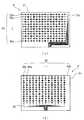
電極層1は、第1面状体2及び第2面状体3を備えている。第1面状体2は、図1の断面図及び図2(a)の平面図に示すように、第1基板21と、第1基板21の一方面上にパターニングされた第1電極22と、当該第1電極22を構成する各電極部22aに電気的に接続する第1引き出し配線23とを備えている。同様に、第2面状体3は、図1の断面図及び図2(b)の平面図に示すように、第2基板31と、第2基板31の一方面上にパターニングされた第2電極32と、当該第2電極32を構成する電極部32aに電気的に接続する第2引き出し配線33とを備えている。第1面状体2と第2面状体3とは、図1に示すように、第1電極22及び第2基板31の他方面側(第2電極32が形成されていない面側)が互いに離間して対向するようにして、粘着層6bを介して貼着されている。なお、第1電極22及び第2電極32が互いに離間して対向するようにして、第1面状体2と第2面状体3とを粘着層6bを介して貼着してもよく、或いは、第1基板21の他方面と第2電極32が互いに離間して対向するように、粘着層6bを介して貼着してもよい。更には、第1基板21の他方面側(第1電極22が形成されていない面側)と、第2基板31の他方面側(第2電極32が形成されていない面側)とが、互いに離間して対向するように粘着層6bを介して第1面状体2と第2面状体3とを貼着し、第1電極22及び第2電極32が互いに反対方向を向くように構成してもよい。 The electrode layer 1 includes a first planar body 2 and a second planar body 3. As shown in the cross-sectional view of FIG. 1 and the plan view of FIG. 2A, the first planar body 2 includes a
第1基板21及び第2基板31は、絶縁層を構成する誘電体基板であり、透明性が高い材料からなることが好ましい。例えば、ポリエチレンテレフタレート(PET)、ポリイミド(PI)、ポリエチレンナフタレート(PEN)、ポリエーテルサルフォン(PES)、ポリエーテルエーテルケトン(PEEK)、ポリカーボネート(PC)、ポリプロピレン(PP)、ポリアミド(PA)、アクリル、非晶性ポリオレフィン系樹脂、環状ポリオレフィン系樹脂、脂肪族環状ポリオレフィン、ノルボルネン系の熱可塑性透明樹脂、シクロオレフィン重合体(COP)又はシクロオレフィン共重合体(COC)からなるシクロオレフィン系樹脂などのなどの合成樹脂製の可撓性フィルムやこれら2種以上の積層体、或いは、ソーダガラス、無アルカリガラス、ホウケイ酸ガラス、石英ガラスなどのガラス板により形成される。第1基板21及び第2基板31の厚みは、特に限定されないが、例えば、合成樹脂製の可撓性フィルムにより第1基板21及び第2基板31を構成する場合には、10μm〜2000μm程度とすることが好ましく、50μm〜500μm程度とすることがさらに好ましい。 The
また、可撓性を有する材料から第1基板21及び第2基板31を形成する場合、当該第1基板21及び第2基板31に剛性を付与するために支持体を貼着してもよい。支持体としては、ガラス板や、ガラスに準ずる硬度を有する樹脂材料を例示することができ、その厚さは100μm以上であることが好ましく、0.2mm〜10mmであることがより好ましい。なお、第1基板21及び第2基板31の表面に、濡れ性向上の為にプラズマ処理を行ったり、表面保護のためのハードコート層や、第1電極22及び第2電極32との密着性改善や光学特性改善の為にアンダーコート層を設けるなど、必要な機能性膜を追加してもよい。 Moreover, when forming the 1st board |
また、第1基板21及び第2基板31を光等方性材料により形成した光等方性フィルムにより構成してもよい。光等方性材料は、入射する全ての光に対して偏光性を有しない材料(リタデーション値が0nm〜10nm程度)で、例えば、ポリカーボネート(PC)、ポリエーテルサルフォン(PES)、ポリアクリル(PAC)、非晶質ポリオリフィン系樹脂、環状ポリオリフィン系樹脂、脂肪族環状ポリオレフィン、ノルボルネン系の熱可塑性透明樹脂、ガラス材料などを例示することができる。これらの材料を用いて第1基板21及び第2基板31を形成する方法としては、キャストや押し出しという手法を用いることができる。 Moreover, you may comprise the 1st board |
第1基板21及び第2基板31の一方の主面上にそれぞれ形成されるパターニングされた第1電極22及び第2電極32は、図2(a)(b)に示すように、それぞれ所定間隔をあけて互いに平行に延びるように形成されている帯状電極部22a,32aの集合体として形成されている。第1電極22及び第2電極32を構成する帯状電極部22a,32aは、複数の菱形状電極体が直線状に連結された構成であり、第1電極22及び第2電極32における菱形状電極部の連結方向が互いに直交し、且つ、平面視において上下の菱形状電極部が重なり合わないように配置されている。なお、第1電極22及び第2電極32のパターン形状は、本実施形態のものに限定されず、指などの接触ポイントを検出可能である限り任意の形状とすることが可能である。例えば、帯状電極部22a,32aの形状として、図5に示すように矩形状とすることも可能である。ただし、タッチパネル100の分解能などの動作性能については、第1面状体2と第2面状体3とを重ね合わせた場合に、電極部22a,32aが存在しない領域を少なくする構成を採用する方が優れている。このような観点から、第1電極22及び第2電極32のパターン形状として、矩形状の構成よりも、複数の菱形状電極部が直線状に連結された構成の方が望ましい。但し、本実施形態のものに限定されず、適切なパターン形状が選択されうる。 As shown in FIGS. 2A and 2B, the patterned
第1電極22及び第2電極32の材料としては、インジウム錫酸化物(ITO)、酸化インジウム、アンチモン添加酸化錫、フッ素添加酸化錫、アルミニウム添加酸化亜鉛、カリウム添加酸化亜鉛、シリコン添加酸化亜鉛や、酸化亜鉛−酸化錫系、酸化インジウム−酸化錫系、酸化亜鉛−酸化インジウム−酸化マグネシウム系、酸化亜鉛、スズ酸化膜等の透明導電材料、或いは、スズ、銅、アルミニウム、ニッケル、クロムなどの金属材料、金属酸化物材料を例示することができ、これら2種以上を複合して形成してもよい。また、酸やアルカリに弱い金属単体でも導電材料として使用できる。 Examples of materials for the
また、カーボンナノチューブやカーボンナノホーン、カーボンナノワイヤ、カーボンナノファイバー、グラファイトフィブリルなどの極細導電炭素繊維や、銀素材等からなる極細導電繊維を、バインダーとして機能するポリマー材料に分散させた複合材を第1電極22及び第2電極32の材料として用いることもできる。ここでポリマー材料としては、ポリアニリン、ポリピロール、ポリアセチレン、ポリチオフェン、ポリフェニレンビニレン、ポリフェニレンスルフィド、ポリp−フェニレン、ポリ複素環ビニレン、PEDOT:poly(3,4-ethylenedioxythiophene)などの導電性ポリマーを採用することができる。また、ポリエチレンテレフタレート(PET)、ポリエチレンナフタレート(PEN)、ポリエーテルサルフォン(PES)、ポリエーテルエーテルケト
ン(PEEK)、ポリカーボネート(PC)、ポリプロピレン(PP)、ポリアミド(PA)、アクリル、ポリイミド、エポキシ樹脂、フェノール樹脂、脂肪族環状ポリオレフィン、ノルボルネン系の熱可塑性透明樹脂などの非導電性ポリマーを採用することができる。In addition, a composite material in which ultrafine conductive carbon fibers such as carbon nanotubes, carbon nanohorns, carbon nanowires, carbon nanofibers, and graphite fibrils, and ultrafine conductive fibers made of silver or the like are dispersed in a polymer material functioning as a binder is first. It can also be used as a material for the
第1電極22及び第2電極32の材料として、特にカーボンナノチューブを非導電性ポリマー材料に分散させたカーボンナノチューブ複合材を採用した場合、カーボンナノチューブは、直径が一般的には0.8nm〜1.4nm(1nm前後)と極めて細いので、1本或いは1束ずつ非導電性ポリマー材料中に分散することでカーボンナノチューブが光透過を阻害することが少なくなり、透明導電膜3の透明性を確保する上で好ましい。 When a carbon nanotube composite material in which carbon nanotubes are dispersed in a non-conductive polymer material is employed as the material of the
第1電極22及び第2電極32の形成方法は、スパッタリング法、真空蒸着法、イオンプレーティング法などのPVD法や、CVD法、塗工法、印刷法などを例示することができる。また、第1電極22及び第2電極32の厚みは、例えばスパッタリング法でITO膜を成膜する場合は、60nm以下であることが好ましく、30nm以下であることがより好ましい。なお、膜厚が5nm以下では連続した膜になり難く、安定な導電層を形成することは困難である。 Examples of the method for forming the
第1電極22及び第2電極32のパターニングは、第1基板21及び第2基板31上に形成されたITO膜等の表面に、所望のパターン形状を有するマスク部を形成して露出部分を酸液などでエッチング除去した後、アルカリ液などによりマスク部を溶解させて行うことができる。 The patterning of the
第1電極22における各帯状電極部22aに電気的に接続する第1引き出し配線23や、第2電極32における各帯状電極部32aに電気的に接続する第2引き出し配線33は、第1電極22及び第2電極32が検出したタッチ信号を、外部に配置されるタッチ位置判別用回路(図示せず)に導くためのものである。図2(a)(b)に示すように、各第1引き出し配線23の一方の端部は、各帯状電極部22aに接続し、他方の端部は、第1基板21の側縁部に配置されている。同様に、各第2引き出し配線33の一方の端部は、各帯状電極部32aに接続し、他方の端部は、第2基板31の側縁部に配置されている。また、第1基板21及び第2基板31の側縁部にそれぞれ配置される第1引き出し配線23及び第2引き出し配線33の一端部分は、所定間隔をあけて一纏まりとなるように配置されている。この一纏まりとなるように配置される第1引き出し配線23及び第2引き出し配線33の一端部分は、接続端子を構成しており、当該接続端子にフレキシブル配線板7が接続される。 The
第1引き出し配線23及び第2引き出し配線33の形成方法は、(A)銀などの金属の導電性粒子を含む導電性ペーストを第1及び第2基板21,31上にスクリーン印刷する方法、(B)銅などの金属箔を第1及び第2基板21,31上に積層し、金属箔の上にレジストパターンを形成し、金属箔をエッチングする方法(特開2008−32884等参照)が挙げられる。また、第1及び第2引き出し配線23,33を上述の第1電極22及び第2電極32と同様の材料(インジウム錫酸化物(ITO)や導電性ポリマー等)により形成してもよい。第1及び第2引き出し配線23,33を第1電極22及び第2電極32と同じ材料で形成する場合、第1電極22及び第2電極32のパターニング手法と同手法や、上記(B)の形成方法、レーザー照射により不要な領域を除去する方法等を採用することができる。 The first lead-
上記(A)の形成方法における導電性粒子としては、銀を主成分とする微粒子を挙げることができる。また、例えば、金、銀、銅、金と銀の合金、金と銅の合金、銀と銅の合金、金と銀と銅の合金のいずれか一を主成分とする微粒子でもよい。また、インジウム錫酸化物(ITO)、酸化インジウムに酸化亜鉛を混合した導電性酸化物(IZO[indium
zinc oxide])、または酸化インジウムに酸化珪素を混合した導電性酸化物(ITSO)を主成分とする微粒子でもよい。また、他の導電性ペーストとして、PEDOT(ポリ−3,4−エチレンジオキシチオフェン)等の導電性高分子や、カーボンナノワイヤーや金属ナノワイヤーなどの極細導電繊維を導電体とする導電性材料を使用することができる。なお、引き出し配線23,33の形成方法は、上記(A)(B)の形成方法に限定されることはなく、上記(A)以外のグラビア印刷などの印刷方法や上記(B)以外のフォトリソグラフィを使用してもよい。Examples of the conductive particles in the forming method (A) include fine particles containing silver as a main component. Further, for example, fine particles mainly containing any one of gold, silver, copper, an alloy of gold and silver, an alloy of gold and copper, an alloy of silver and copper, and an alloy of gold, silver, and copper may be used. In addition, indium tin oxide (ITO), conductive oxide in which zinc oxide is mixed with indium oxide (IZO [indium
zinc oxide]), or fine particles mainly composed of conductive oxide (ITSO) in which silicon oxide is mixed with indium oxide. In addition, as another conductive paste, a conductive material using a conductive polymer such as PEDOT (poly-3,4-ethylenedioxythiophene), or a fine conductive fiber such as carbon nanowire or metal nanowire as a conductor. Can be used. The formation method of the lead-
粘着層6a,6b,6cは、エポキシ系やアクリル系など、一般的な透明接着剤を用いることができ、ポリエステル系樹脂の透明性フィルムからなる芯材を含むものであってもよい。また、シート状粘着材を複数枚重ね合わせることにより粘着層6a,6b,6cを形成してもよく、更に、複数種類のシート状粘着材を重ね合わせて形成してもよい。粘着層6a,6b,6cの厚みは、特に指定はないが、実用上では20μmから500μmであることが好ましい。 The
フレキシブル配線板7は、フィルム状で柔軟性があり、自由に曲げることのできる配線板であり、第1面状体2、第2面状体3からなる電極層1の側方から外部へ引き出されるように配置される。本実施形態におけるフレキシブル配線板7は、図3に示すように、先端部が二股状に分割された形状を有するコネクタ部71を備えており、一方が、図1の断面図に示すように第2引き出し配線32の接続端子に重ね合わされて電気的に接続する第1コネクタ部71aを構成し、他方が、図4の断面図に示すように第1引き出し配線23の接続端子に重ね合わされて電気的に接続する第2コネクタ部71bを構成している。第1コネクタ部71a及び第2コネクタ部71bは、略同一の厚みを有するように構成されている。なお、コネクタ部71は、絶縁性の高い接着剤中に導電粒子を均一分散させた異方性導電接着剤により引き出し配線の接続端子に接続されている。 The
また、上記構成においては、フレキシブル配線板7のコネクタ部71が二股状に分割された形状を有するように構成し、一方を、第1引き出し配線23の接続端子に接続すると共に、他方を、第2引き出し配線33の接続端子と接続するように構成しているが、例えば、2つのフレキシブル配線板7を準備し、各フレキシブル配線板7をそれぞれ第1引き出し配線23の接続端子及び第2引き出し配線33の接続端子に接続するように構成してもよい。 Further, in the above configuration, the
以上の構成を備えるタッチパネル100において、タッチ位置の検出方法は、従来の静電容量式のタッチスイッチと同様であり、タッチパネル100の表面側における任意の位置を指などで触れると、電極層1における第1電極22及び第2電極32は接触位置において人体の静電容量を介して接地され、第1電極22及び第2電極32を流れる電流値を検出すること(人体との間の静電容量の変化を検出すること)により、接触位置の座標が演算される。 In
本実施形態のタッチパネル100は、直線偏光板5と、λ/4位相差板4とを備えているため、ディスプレイ表面8aにおいて反射する反射光を効果的にカットすることができ、ディスプレイに表示される文字情報や画像情報の視認性を向上させることが可能となる。具体的に説明すると、タッチパネル100に入射した外光は、直線偏光板5を通過する際に水平の直線偏光に偏光されて、電極層1を通過し、λ/4位相差板4に入射する。λ/4位相差板4に入射した水平の直線偏光は、右回りの円偏光に偏光されて、ディスプレイ表面8aにて反射する。反射した右回りの円偏光は、反射時に左回りの円偏光になり、再度λ/4位相差板4に入射する。λ/4位相差板4に入射した左回りの円偏光は、λ/4位相差板4通過時に垂直の直線偏光に偏光されて、電極層1を通過して直線偏光板5に入射する。直線偏光板5に入射した垂直の直線偏光は、この直線偏光板5を通過することができないため、ディスプレイ表面8aでの反射光が視認できなくなる。このように直線偏光板5とλ/4位相差板4とを備えることにより、ディスプレイ表面8aでの反射を防止できる結果、ディスプレイにより表示される文字情報や画像情報の視認性を向上させることができる。 Since the
また、フレキシブル配線板7が接続される電極層1を直線偏光板5とλ/4位相差板4とで挟み込む形態を有しているため、直線偏光板5及びλ/4位相差板4が電極層1の補強板として機能することとなり、フレキシブル配線板7を屈曲させて外部のタッチ位置判別用回路に接続する場合に、フレキシブル配線板7のコネクタ部71と引き出し配線23,33との接続個所において大きな曲げ応力が発生することを効果的に抑制することができる。この結果、電極層1を構成する第1面状体2や第2面状体3が、折れ曲がったり、割れてしまうことを効果的に防止することができる。 Further, since the electrode layer 1 to which the
特に、電極層1における第1基板21や第2基板31を光等方性材料により構成した場合、光等方性材料からなる第1基板21や第2基板31は脆くて割れやすいという問題を有するが、本発明のように、電極層1の両側に直線偏光板5及びλ/4位相差板4をそれぞれ配置する構成を採用することにより、フレキシブル配線板7の屈曲時に第1基板21や第2基板31が割れてしまうことを極めて効果的に防止することが可能となる。 In particular, when the
以上、本発明に係るタッチパネル100の一実施形態について説明したが、具体的構成は、上記実施形態に限定されない。例えば、上記実施形態において、直線偏光板5の露出面(タッチ面)に、タッチパネル100保護用のカバーガラスや、耐指紋フィルムや反射防止フィルム等のカバーフィルムを配置するように構成してもよい。また、λ/4位相差板4の一方面(ディスプレイ表面8aとの対向面)に、傷付防止用のハードコート層や、アンチグレア(防眩)処理層等を設けるように構成してもよい。 As mentioned above, although one Embodiment of the
また、上記実施形態においては、電極層1の構成として、第1面状体2と第2面状体3とを備えるように構成し、それぞれが第1電極22及び第2電極32を備えるように構成しているが、例えば、第2面状体3を省略し、第1面状体2における第1基板21の両面に、第1電極22及び第2電極32をそれぞれ形成するようにして電極層1を構成してもよい。または、第1基板21の片側表面に、第1電極22及び第2電極32をそれぞれ形成(第1電極22及び第2電極32の重なり部分は絶縁)するようにして電極層1を構成してもよい。または、第1基板21の片側表面に、第1電極22を形成した上に誘電体層を形成し、さらに第2電極32形成するようにして電極層1を構成してもよい。 In the above embodiment, the electrode layer 1 is configured to include the first planar body 2 and the second planar body 3, and each includes the
また、上記実施形態においては、図1に示すように、表示装置8のディスプレイ表面8aに第2λ/4位相差板10を配置することが好ましい。第2λ/4位相差板10を備えるように構成する場合、当該第2λ/4位相差板10の遅相軸と、λ/4位相差板4の遅相軸とが90度の角度をなすように、第2λ/4位相差板10は配置される。このような構成を採用することにより、表示装置8から照射される光の位相のずれを打ち消しあうことができるため、タッチパネル100の視認性を向上させることが可能となる。 Moreover, in the said embodiment, as shown in FIG. 1, it is preferable to arrange | position the 2 (lambda) / 4
100 タッチパネル
1 電極層
2 第1面状体
21 第1基板
22 第1電極
23 第1引き出し配線
3 第2面状体
31 第2基板
31a 切欠き部
32 第2電極
33 第2引き出し配線
4 λ/4位相差板
5 直線偏光板
6a、6b、6c 粘着層
7 フレキシブル配線板
71 コネクタ部
71a 第1コネクタ部
71b 第2コネクタ部
8 表示装置
8a ディスプレイ表面DESCRIPTION OF
Claims (5)
Translated fromJapanese前記表示装置側から順に、λ/4位相差板、タッチ位置検出用の電極層及び直線偏光板が配置されており、
前記電極層上に前記直線偏光板が積層されていることを特徴とするタッチパネル。A touch panel installed on the display device by providing an air layer between the display surface of the display device,
In order from the display device side, aλ / 4 phase difference plate, an electrode layer for touch position detection, and alinear polarizing plate are arranged,
The touch panel, wherein thelinearly polarizing plate is laminated on the electrode layer.
前記第1引き出し配線の接続端子とする一端部分が配置される前記第1基板の側縁部において前記第1引き出し配線の一端部分に重ね合わせて電気的に接続する第1コネクタ部を有し、前記第1面状体の側方から外部へ引き出されるフレキシブル配線板を備える請求項1に記載のタッチパネル。The electrode layer includes a first planar body having a first electrode patterned on one surface of a first substrate and a first lead wiring electrically connected to the first electrode;
A first connector portion that overlaps and electrically connects to one end portion of the first lead-out wiring at a side edge portion of the first substrate where one end portion serving as a connection terminal of the first lead-out wiring is disposed; The touch panel as set forth in claim 1, further comprising a flexible wiring board drawn out from a side of the first planar body.
前記第1引き出し配線の接続端子とする一端部分が配置される前記第1基板の側縁部において、前記第1引き出し配線の一端部分に重ね合わせて電気的に接続する第1コネクタ部と、前記第2引き出し配線の接続端子とする一端部分が配置される前記第2基板の側縁部において、前記第2引き出し配線の一端部分に重ね合わせて電気的に接続する第2コネクタ部とを有し、前記電極層の側方から外部へ引き出されるフレキシブル配線板を備える請求項1に記載のタッチパネル。The electrode layer has a first electrode patterned on one surface of the first substrate, a first planar body having a first lead wire electrically connected to the first electrode, and one surface of the second substrate. And a second planar body having a second electrode patterned and a second lead wiring electrically connected to the second electrode,
A first connector portion that overlaps and is electrically connected to one end portion of the first lead wiring at a side edge portion of the first substrate where one end portion serving as a connection terminal of the first lead wiring is disposed; A second connector portion that overlaps and electrically connects to one end portion of the second lead-out wiring at a side edge portion of the second substrate on which one end portion serving as a connection terminal of the second lead-out wiring is disposed; The touch panel according to claim 1, further comprising a flexible wiring board drawn out from a side of the electrode layer.
The touch panel according to any one of claims 1 to 4, wherein a touch position is detected based on a change in capacitance between the electrode layer and a human body.
Priority Applications (1)
| Application Number | Priority Date | Filing Date | Title |
|---|---|---|---|
| JP2012210193AJP6127251B2 (en) | 2012-09-24 | 2012-09-24 | Touch panel |
Applications Claiming Priority (1)
| Application Number | Priority Date | Filing Date | Title |
|---|---|---|---|
| JP2012210193AJP6127251B2 (en) | 2012-09-24 | 2012-09-24 | Touch panel |
Publications (2)
| Publication Number | Publication Date |
|---|---|
| JP2014067103A JP2014067103A (en) | 2014-04-17 |
| JP6127251B2true JP6127251B2 (en) | 2017-05-17 |
Family
ID=50743469
Family Applications (1)
| Application Number | Title | Priority Date | Filing Date |
|---|---|---|---|
| JP2012210193AActiveJP6127251B2 (en) | 2012-09-24 | 2012-09-24 | Touch panel |
Country Status (1)
| Country | Link |
|---|---|
| JP (1) | JP6127251B2 (en) |
Families Citing this family (4)
| Publication number | Priority date | Publication date | Assignee | Title |
|---|---|---|---|---|
| WO2015194074A1 (en)* | 2014-06-18 | 2015-12-23 | パナソニックIpマネジメント株式会社 | Capacitive touch panel |
| JP6085647B2 (en)* | 2015-08-11 | 2017-02-22 | 株式会社フジクラ | Wiring assembly, structure with conductor layer, and touch sensor |
| KR102548931B1 (en)* | 2016-03-22 | 2023-06-30 | 삼성디스플레이 주식회사 | Display device |
| US10788943B2 (en) | 2016-12-15 | 2020-09-29 | Sharp Kabushiki Kaisha | Touch panel-equipped display device |
Family Cites Families (5)
| Publication number | Priority date | Publication date | Assignee | Title |
|---|---|---|---|---|
| EP1892609A4 (en)* | 2005-05-26 | 2013-03-27 | Gunze Kk | Transparent planar body and transparent touch switch |
| JP2008262326A (en)* | 2007-04-11 | 2008-10-30 | Matsushita Electric Ind Co Ltd | Touch panel |
| JP5601944B2 (en)* | 2010-06-28 | 2014-10-08 | 帝人株式会社 | Touch panel device and display device with touch panel device |
| CN102834796B (en)* | 2010-07-07 | 2016-04-27 | 阿尔卑斯电气株式会社 | input device |
| JP2012027622A (en)* | 2010-07-21 | 2012-02-09 | Nissha Printing Co Ltd | Capacitance touch sensor and liquid crystal display device having capacitance touch input function |
- 2012
- 2012-09-24JPJP2012210193Apatent/JP6127251B2/enactiveActive
Also Published As
| Publication number | Publication date |
|---|---|
| JP2014067103A (en) | 2014-04-17 |
Similar Documents
| Publication | Publication Date | Title |
|---|---|---|
| JP5078534B2 (en) | Transparent sheet and transparent touch switch | |
| JP5569891B2 (en) | Touch panel and manufacturing method thereof | |
| CN100552606C (en) | Transparent planar body and transparent touch switch | |
| JP6098787B2 (en) | Display device with touch panel | |
| US10481743B2 (en) | High-performance touch sensor and manufacturing method thereof | |
| JP5512624B2 (en) | Capacitive touch sensor and display device having the same | |
| JP5374457B2 (en) | Planar body and touch panel | |
| TW201523386A (en) | Composite polarizing plate-integrated touch sensing electrode and touch screen panel including the same | |
| JP2014229136A (en) | Touch panel, display device and electronic device | |
| JP6127251B2 (en) | Touch panel | |
| JP2015035173A (en) | Display device with input function | |
| JP6477164B2 (en) | Intermediate member for touch panel sensor, and electrical inspection method for intermediate member for touch panel sensor | |
| JP6134968B2 (en) | Display device | |
| JP6134965B2 (en) | Touch panel device | |
| JP2012226498A (en) | Touch switch | |
| JP6610107B2 (en) | Image display device | |
| JP2016194746A (en) | Intermediate member for touch panel sensor and method for manufacturing touch panel sensor | |
| JP2016194751A (en) | Touch panel sensor | |
| JP2015164007A (en) | Touch panel sensor, touch panel device, display device, and method for manufacturing touch panel sensor |
Legal Events
| Date | Code | Title | Description |
|---|---|---|---|
| A621 | Written request for application examination | Free format text:JAPANESE INTERMEDIATE CODE: A621 Effective date:20150605 | |
| A977 | Report on retrieval | Free format text:JAPANESE INTERMEDIATE CODE: A971007 Effective date:20160413 | |
| A131 | Notification of reasons for refusal | Free format text:JAPANESE INTERMEDIATE CODE: A131 Effective date:20160415 | |
| A521 | Request for written amendment filed | Free format text:JAPANESE INTERMEDIATE CODE: A523 Effective date:20160430 | |
| A521 | Request for written amendment filed | Free format text:JAPANESE INTERMEDIATE CODE: A523 Effective date:20160430 | |
| A131 | Notification of reasons for refusal | Free format text:JAPANESE INTERMEDIATE CODE: A131 Effective date:20160810 | |
| A131 | Notification of reasons for refusal | Free format text:JAPANESE INTERMEDIATE CODE: A131 Effective date:20170105 | |
| A521 | Request for written amendment filed | Free format text:JAPANESE INTERMEDIATE CODE: A523 Effective date:20170219 | |
| TRDD | Decision of grant or rejection written | ||
| A01 | Written decision to grant a patent or to grant a registration (utility model) | Free format text:JAPANESE INTERMEDIATE CODE: A01 Effective date:20170303 | |
| A61 | First payment of annual fees (during grant procedure) | Free format text:JAPANESE INTERMEDIATE CODE: A61 Effective date:20170308 | |
| R150 | Certificate of patent or registration of utility model | Ref document number:6127251 Country of ref document:JP Free format text:JAPANESE INTERMEDIATE CODE: R150 | |
| R250 | Receipt of annual fees | Free format text:JAPANESE INTERMEDIATE CODE: R250 | |
| R250 | Receipt of annual fees | Free format text:JAPANESE INTERMEDIATE CODE: R250 | |
| R250 | Receipt of annual fees | Free format text:JAPANESE INTERMEDIATE CODE: R250 | |
| R250 | Receipt of annual fees | Free format text:JAPANESE INTERMEDIATE CODE: R250 | |
| R250 | Receipt of annual fees | Free format text:JAPANESE INTERMEDIATE CODE: R250 | |
| S111 | Request for change of ownership or part of ownership | Free format text:JAPANESE INTERMEDIATE CODE: R313113 | |
| R250 | Receipt of annual fees | Free format text:JAPANESE INTERMEDIATE CODE: R250 | |
| R350 | Written notification of registration of transfer | Free format text:JAPANESE INTERMEDIATE CODE: R350 |