JP6126775B2 - Display device - Google Patents
Display deviceDownload PDFInfo
- Publication number
- JP6126775B2 JP6126775B2JP2011136107AJP2011136107AJP6126775B2JP 6126775 B2JP6126775 B2JP 6126775B2JP 2011136107 AJP2011136107 AJP 2011136107AJP 2011136107 AJP2011136107 AJP 2011136107AJP 6126775 B2JP6126775 B2JP 6126775B2
- Authority
- JP
- Japan
- Prior art keywords
- pixel electrode
- electrode
- pixel
- gap
- pixel electrodes
- Prior art date
- Legal status (The legal status is an assumption and is not a legal conclusion. Google has not performed a legal analysis and makes no representation as to the accuracy of the status listed.)
- Active
Links
Images


Classifications
- G—PHYSICS
- G02—OPTICS
- G02F—OPTICAL DEVICES OR ARRANGEMENTS FOR THE CONTROL OF LIGHT BY MODIFICATION OF THE OPTICAL PROPERTIES OF THE MEDIA OF THE ELEMENTS INVOLVED THEREIN; NON-LINEAR OPTICS; FREQUENCY-CHANGING OF LIGHT; OPTICAL LOGIC ELEMENTS; OPTICAL ANALOGUE/DIGITAL CONVERTERS
- G02F1/00—Devices or arrangements for the control of the intensity, colour, phase, polarisation or direction of light arriving from an independent light source, e.g. switching, gating or modulating; Non-linear optics
- G02F1/01—Devices or arrangements for the control of the intensity, colour, phase, polarisation or direction of light arriving from an independent light source, e.g. switching, gating or modulating; Non-linear optics for the control of the intensity, phase, polarisation or colour
- G02F1/165—Devices or arrangements for the control of the intensity, colour, phase, polarisation or direction of light arriving from an independent light source, e.g. switching, gating or modulating; Non-linear optics for the control of the intensity, phase, polarisation or colour based on translational movement of particles in a fluid under the influence of an applied field
- G02F1/166—Devices or arrangements for the control of the intensity, colour, phase, polarisation or direction of light arriving from an independent light source, e.g. switching, gating or modulating; Non-linear optics for the control of the intensity, phase, polarisation or colour based on translational movement of particles in a fluid under the influence of an applied field characterised by the electro-optical or magneto-optical effect
- G02F1/167—Devices or arrangements for the control of the intensity, colour, phase, polarisation or direction of light arriving from an independent light source, e.g. switching, gating or modulating; Non-linear optics for the control of the intensity, phase, polarisation or colour based on translational movement of particles in a fluid under the influence of an applied field characterised by the electro-optical or magneto-optical effect by electrophoresis
- G—PHYSICS
- G02—OPTICS
- G02F—OPTICAL DEVICES OR ARRANGEMENTS FOR THE CONTROL OF LIGHT BY MODIFICATION OF THE OPTICAL PROPERTIES OF THE MEDIA OF THE ELEMENTS INVOLVED THEREIN; NON-LINEAR OPTICS; FREQUENCY-CHANGING OF LIGHT; OPTICAL LOGIC ELEMENTS; OPTICAL ANALOGUE/DIGITAL CONVERTERS
- G02F1/00—Devices or arrangements for the control of the intensity, colour, phase, polarisation or direction of light arriving from an independent light source, e.g. switching, gating or modulating; Non-linear optics
- G02F1/01—Devices or arrangements for the control of the intensity, colour, phase, polarisation or direction of light arriving from an independent light source, e.g. switching, gating or modulating; Non-linear optics for the control of the intensity, phase, polarisation or colour
- G02F1/165—Devices or arrangements for the control of the intensity, colour, phase, polarisation or direction of light arriving from an independent light source, e.g. switching, gating or modulating; Non-linear optics for the control of the intensity, phase, polarisation or colour based on translational movement of particles in a fluid under the influence of an applied field
- G02F1/1675—Constructional details
- G02F1/1676—Electrodes
- G02F1/16766—Electrodes for active matrices
- G—PHYSICS
- G09—EDUCATION; CRYPTOGRAPHY; DISPLAY; ADVERTISING; SEALS
- G09G—ARRANGEMENTS OR CIRCUITS FOR CONTROL OF INDICATING DEVICES USING STATIC MEANS TO PRESENT VARIABLE INFORMATION
- G09G3/00—Control arrangements or circuits, of interest only in connection with visual indicators other than cathode-ray tubes
- G09G3/20—Control arrangements or circuits, of interest only in connection with visual indicators other than cathode-ray tubes for presentation of an assembly of a number of characters, e.g. a page, by composing the assembly by combination of individual elements arranged in a matrix no fixed position being assigned to or needed to be assigned to the individual characters or partial characters
- G09G3/34—Control arrangements or circuits, of interest only in connection with visual indicators other than cathode-ray tubes for presentation of an assembly of a number of characters, e.g. a page, by composing the assembly by combination of individual elements arranged in a matrix no fixed position being assigned to or needed to be assigned to the individual characters or partial characters by control of light from an independent source
- G09G3/3433—Control arrangements or circuits, of interest only in connection with visual indicators other than cathode-ray tubes for presentation of an assembly of a number of characters, e.g. a page, by composing the assembly by combination of individual elements arranged in a matrix no fixed position being assigned to or needed to be assigned to the individual characters or partial characters by control of light from an independent source using light modulating elements actuated by an electric field and being other than liquid crystal devices and electrochromic devices
- G09G3/344—Control arrangements or circuits, of interest only in connection with visual indicators other than cathode-ray tubes for presentation of an assembly of a number of characters, e.g. a page, by composing the assembly by combination of individual elements arranged in a matrix no fixed position being assigned to or needed to be assigned to the individual characters or partial characters by control of light from an independent source using light modulating elements actuated by an electric field and being other than liquid crystal devices and electrochromic devices based on particles moving in a fluid or in a gas, e.g. electrophoretic devices
- G09G3/3446—Control arrangements or circuits, of interest only in connection with visual indicators other than cathode-ray tubes for presentation of an assembly of a number of characters, e.g. a page, by composing the assembly by combination of individual elements arranged in a matrix no fixed position being assigned to or needed to be assigned to the individual characters or partial characters by control of light from an independent source using light modulating elements actuated by an electric field and being other than liquid crystal devices and electrochromic devices based on particles moving in a fluid or in a gas, e.g. electrophoretic devices with more than two electrodes controlling the modulating element
- G—PHYSICS
- G02—OPTICS
- G02F—OPTICAL DEVICES OR ARRANGEMENTS FOR THE CONTROL OF LIGHT BY MODIFICATION OF THE OPTICAL PROPERTIES OF THE MEDIA OF THE ELEMENTS INVOLVED THEREIN; NON-LINEAR OPTICS; FREQUENCY-CHANGING OF LIGHT; OPTICAL LOGIC ELEMENTS; OPTICAL ANALOGUE/DIGITAL CONVERTERS
- G02F2201/00—Constructional arrangements not provided for in groups G02F1/00 - G02F7/00
- G02F2201/12—Constructional arrangements not provided for in groups G02F1/00 - G02F7/00 electrode
- G02F2201/123—Constructional arrangements not provided for in groups G02F1/00 - G02F7/00 electrode pixel
- G—PHYSICS
- G09—EDUCATION; CRYPTOGRAPHY; DISPLAY; ADVERTISING; SEALS
- G09G—ARRANGEMENTS OR CIRCUITS FOR CONTROL OF INDICATING DEVICES USING STATIC MEANS TO PRESENT VARIABLE INFORMATION
- G09G2310/00—Command of the display device
- G09G2310/02—Addressing, scanning or driving the display screen or processing steps related thereto
- G09G2310/0264—Details of driving circuits
- G09G2310/0272—Details of drivers for data electrodes, the drivers communicating data to the pixels by means of a current
Landscapes
- Physics & Mathematics (AREA)
- Nonlinear Science (AREA)
- General Physics & Mathematics (AREA)
- Optics & Photonics (AREA)
- Engineering & Computer Science (AREA)
- Theoretical Computer Science (AREA)
- Computer Hardware Design (AREA)
- Molecular Biology (AREA)
- Electrochemistry (AREA)
- Chemical Kinetics & Catalysis (AREA)
- Chemical & Material Sciences (AREA)
- Life Sciences & Earth Sciences (AREA)
- Health & Medical Sciences (AREA)
- Electrochromic Elements, Electrophoresis, Or Variable Reflection Or Absorption Elements (AREA)
- Devices For Indicating Variable Information By Combining Individual Elements (AREA)
- Vehicle Body Suspensions (AREA)
- Diaphragms For Electromechanical Transducers (AREA)
- Measuring Pulse, Heart Rate, Blood Pressure Or Blood Flow (AREA)
Description
Translated fromJapanese技術分野は、表示装置及びその駆動方法に関する。また、表示装置の作製方法に関する。 The technical field relates to a display device and a driving method thereof. Further, the present invention relates to a method for manufacturing a display device.
近年、デジタル化技術の進歩に伴い、新聞、雑誌などの文字情報や画像情報を電子データとして提供できるようになっている。この種の電子データは、一般に、テレビ、パーソナルコンピュータ、または携帯型電子端末などが備える表示装置に表示されることで、その内容が閲覧される。 In recent years, with the advance of digitization technology, character information and image information such as newspapers and magazines can be provided as electronic data. This type of electronic data is generally viewed by being displayed on a display device provided in a television, personal computer, portable electronic terminal, or the like.
そして、紙面と同等の高い視認性を有する表示装置として、電気泳動素子などの電子インクを用いたものが開発されている。電子インクを用いた表示装置としては、例えば、画素電極と対向電極との間にマイクロカプセルを有するものが挙げられる。2つの電極間に電圧を印加し、マイクロカプセル中に存在する着色された粒子を電界方向に移動させることで、表示を行うものである(特許文献1参照)。 As a display device having high visibility equivalent to that of the paper surface, a display device using electronic ink such as an electrophoretic element has been developed. As a display device using electronic ink, for example, a display device having a microcapsule between a pixel electrode and a counter electrode can be given. Display is performed by applying a voltage between the two electrodes and moving the colored particles present in the microcapsule in the direction of the electric field (see Patent Document 1).
上記特許文献1では、表示画像を切り替える際に、残像が生じるという問題があった。 In the above-mentioned Patent Document 1, there is a problem that an afterimage is generated when a display image is switched.
その原因の一つとして、図13(A)に示すように、画素電極5001の端部5003が直線形状であることが挙げられる。端部5003が直線形状であると、表示を行った際に、図13(B)に示すように、画素電極間の隙間5005において電界が正しく印加されない可能性があるため、残像が生じてしまう。なお、残像を消すために初期化処理を行う場合、表示速度が遅くなってしまう。 One of the causes is that the
上記問題に鑑み、残像の低減をはじめとする表示装置の諸性能を向上することを課題の一とする。 In view of the above problems, an object is to improve various performances of a display device including reduction of afterimages.
本明細書で開示する表示装置は、帯電物質に電界を印加することで表示を行う装置である。複数の画素電極を有し、隣接する2つの画素電極の端部の一部又は全部を直線形状としないことで、画素電極間の隙間において、帯電物質に正しく電界を印加するものである。 The display device disclosed in this specification is a device that performs display by applying an electric field to a charged substance. By having a plurality of pixel electrodes and not forming a part or all of the ends of two adjacent pixel electrodes in a straight line shape, an electric field is correctly applied to the charged substance in the gap between the pixel electrodes.
本発明の一態様は、複数の画素電極と、画素電極上に設けられた帯電層(帯電物質を有する層とも呼ぶ)とを有し、複数の画素電極のうち隣接する2つの画素電極の端部は、端面方向に屈曲している部分(屈曲部ともいう)を有する表示装置である。本明細書において、端面方向とは、画素電極の上面に対して平行な方向を指す。また、屈曲している部分は、頂点を有する形状(折れている形状ともいう)でもよく、頂点を有さない形状(曲がっている形状ともいう)でもよい。そして、2つの画素電極における屈曲している部分が、互いに噛み合っていることが好ましい。 One embodiment of the present invention includes a plurality of pixel electrodes and a charged layer (also referred to as a layer having a charged substance) provided over the pixel electrodes, and the ends of two adjacent pixel electrodes among the plurality of pixel electrodes. The portion is a display device having a portion bent also in the end face direction (also referred to as a bent portion). In this specification, the end surface direction refers to a direction parallel to the upper surface of the pixel electrode. Further, the bent portion may be a shape having a vertex (also referred to as a bent shape) or a shape not having a vertex (also referred to as a bent shape). The bent portions of the two pixel electrodes are preferably engaged with each other.
本発明の他の一態様は、複数の画素電極と、画素電極上に設けられた帯電層とを有し、複数の画素電極のうち隣接する2つの画素電極の間において、一方の画素電極の端部は端面方向に凹部(又は凹凸部)を有し、他方の画素電極の端部は端面方向に凸部(又は凹凸部)を有し、一方の画素電極の凹部(又は凹凸部)と、他方の画素電極の凸部(又は凹凸部)とが対になることで、2つの画素電極の間に隙間が形成されている表示装置である。本明細書において、凹部と凸部が対(又は凹凸部が対)になるとは、凹部に対し、凸部が入り込んでいる状態を指す。また、この状態を、凹部と凸部が互いに噛み合っていると表現してもよい。 Another embodiment of the present invention includes a plurality of pixel electrodes and a charging layer provided on the pixel electrode, and one pixel electrode is disposed between two adjacent pixel electrodes among the plurality of pixel electrodes. The end portion has a concave portion (or uneven portion) in the end face direction, the end portion of the other pixel electrode has a convex portion (or uneven portion) in the end face direction, and the concave portion (or uneven portion) of one pixel electrode In the display device, a gap is formed between two pixel electrodes by forming a pair with a convex portion (or an uneven portion) of the other pixel electrode. In this specification, the phrase “a concave portion and a convex portion are paired (or a concave and convex portion is a pair)” refers to a state in which the convex portion enters the concave portion. Moreover, you may express this state as a recessed part and a convex part mutually meshing | engaged.
本発明の他の一態様は、複数の画素電極と、画素電極上に設けられた帯電層とを有し、複数の画素電極のうち隣接する2つの画素電極の間に隙間が形成されており、隙間は三カ所以上の間隔が等しい部分を有し、三カ所以上の部分において、各々の間隔の中点を線分で結ぶと、一つ以上の頂点を有する表示装置である。 Another embodiment of the present invention includes a plurality of pixel electrodes and a charging layer provided on the pixel electrode, and a gap is formed between two adjacent pixel electrodes among the plurality of pixel electrodes. The gap has a portion having equal intervals at three or more places, and the three or more portions are display devices having one or more vertices when the midpoints of the intervals are connected by line segments.
本発明の他の一態様は、複数の画素電極と、画素電極上に設けられた帯電層とを有し、複数の画素電極のうち隣接する2つの画素電極の間において、2つの画素電極の端部はともに屈曲し、且つ、隙間を形成しており、隙間は、三カ所以上の間隔が等しい部分を有する表示装置である。 Another embodiment of the present invention includes a plurality of pixel electrodes and a charging layer provided on the pixel electrode, and the two pixel electrodes are disposed between two adjacent pixel electrodes among the plurality of pixel electrodes. Both end portions are bent and a gap is formed, and the gap is a display device having a portion having three or more equal intervals.
本発明の他の一態様は、複数の画素電極と、画素電極上に設けられた帯電層とを有し、複数の画素電極のうち一の画素電極の右辺の端部と、一の画素電極の右辺において隣接する画素電極の左辺の端部とが屈曲し、且つ、隙間を形成しており、一の画素電極の上辺の端部と、一の画素電極の上辺において隣接する画素電極の下辺の端部とが屈曲し、且つ、隙間を形成しており、前記一の画素電極の右辺における隙間と、前記一の画素電極の上辺における隙間とは、二カ所以上の間隔が等しい部分を有する表示装置である。 Another embodiment of the present invention includes a plurality of pixel electrodes and a charging layer provided on the pixel electrode, and an end portion on the right side of one pixel electrode of the plurality of pixel electrodes and one pixel electrode The edge of the left side of the adjacent pixel electrode is bent and forms a gap, and the edge of the upper side of one pixel electrode and the lower side of the adjacent pixel electrode on the upper side of the one pixel electrode Are bent and form a gap, and the gap on the right side of the one pixel electrode and the gap on the upper side of the one pixel electrode have two or more equal portions. It is a display device.
残像の低減など表示装置の性能を向上させることができる。 The performance of the display device can be improved such as reduction of afterimages.
以下に、実施の形態について、図面を用いて詳細に説明する。但し、以下の実施の形態は多くの異なる態様で実施することが可能であり、趣旨及びその範囲から逸脱することなくその形態及び詳細を様々に変更し得ることは、当業者であれば容易に理解される。従って、以下に示す実施の形態の記載内容に限定して解釈されるものではない。なお、実施の形態を説明するための全図において、同一部分又は同様な機能を有する部分には同一の符号を付し、その繰り返しの説明は省略する。 Hereinafter, embodiments will be described in detail with reference to the drawings. However, the following embodiments can be implemented in many different modes, and it is easy for those skilled in the art to change the modes and details in various ways without departing from the spirit and scope thereof. Understood. Therefore, the present invention is not construed as being limited to the description of the embodiments below. Note that in all the drawings for describing the embodiments, the same portions or portions having similar functions are denoted by the same reference numerals, and repetitive description thereof is omitted.
(実施の形態1)
本実施の形態では、表示装置の構造の一例について説明する。(Embodiment 1)
In this embodiment, an example of a structure of a display device is described.
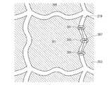
図1は、表示装置の画素部の上面図である。なお、図1では画素部の一部を示している。 FIG. 1 is a top view of a pixel portion of a display device. FIG. 1 shows a part of the pixel portion.
画素部は、複数の画素を有し、該複数の画素は、それぞれ画素電極101を有している。本発明の一態様は、画素電極101の端部の一部又は全部が直線形状ではないことを特徴としている。すなわち、画素電極101の端部が、端面方向に屈曲している部分103を有している。なお、直線形状である部分105を有していてもよい。そして、隣接する2つの画素電極101における屈曲している部分103と部分104とが、互いに噛み合っていることが好ましい。 The pixel portion includes a plurality of pixels, and each of the plurality of pixels includes a
ここで、画素電極101の構造の詳細な条件について、図1の拡大図である図2乃至図5を用いて説明する。 Here, detailed conditions of the structure of the
まず条件1を説明する。隣接する2つの画素電極の間において、一方の画素電極の端部は端面方向に凹部を有し、他方の画素電極の端部は端面方向に凸部を有している。そして、一方の画素電極の凹部と他方の画素電極の凸部とが対になり、2つの画素電極の間に隙間が形成されている。また、2つの画素電極の端部に凹凸部(凹部及び凸部とも呼ぶ)を有し、一方の画素電極の凹凸部と他方の画素電極の凹凸部が対になっていてもよい。 First, condition 1 will be described. Between two adjacent pixel electrodes, an end portion of one pixel electrode has a concave portion in the end surface direction, and an end portion of the other pixel electrode has a convex portion in the end surface direction. Then, the concave portion of one pixel electrode and the convex portion of the other pixel electrode are paired to form a gap between the two pixel electrodes. In addition, an uneven portion (also referred to as a concave portion and a convex portion) may be provided at the end portions of the two pixel electrodes, and the uneven portion of one pixel electrode and the uneven portion of the other pixel electrode may be paired.
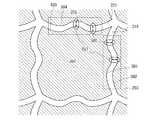
条件1の具体例を、図2に示す。画素電極201は凹部211及び凸部213を有し、画素電極203は凹部215及び凸部217を有している。そして、画素電極201の凹部211と画素電極203の凸部217とが対になり、画素電極201の凸部213と画素電極203の凹部215とが対になっている。すなわち、画素電極201の凹凸部と画素電極203の凹凸部とが対になり、2つの画素電極201、203の間に隙間219が形成されている。条件1を適用することで、図1における画素電極の突出する部分103が形成される。 A specific example of condition 1 is shown in FIG. The
また、別の条件2を説明する。隣接する2つの画素電極の間に隙間が形成されており、該隙間は三カ所以上の間隔が等しい部分を有する。そして、該三カ所以上の部分において、各々の間隔の中点を線分で結ぶと、一つ以上の頂点を有する。すなわち、該三カ所以上の部分における各々の間隔の中点が、一直線上に並ばないことを意味している。 Another condition 2 will be described. A gap is formed between two adjacent pixel electrodes, and the gap has three or more equal portions. And in these three or more parts, when the midpoint of each space | interval is connected with a line segment, it has one or more vertexes. That is, it means that the midpoints of the intervals in the three or more portions are not aligned on a straight line.
条件2の具体例を、図3に示す。隣接する2つの画素電極201、203の間に隙間219が形成されており、隙間219は三カ所の間隔が等しい部分301、303、305を有する。そして、三カ所における各々の間隔の中点を線分で結ぶと、一つの頂点307を有する。条件2を適用することで、図1における画素電極の突出する部分103が形成される。 A specific example of condition 2 is shown in FIG. A
また、別の条件3を説明する。隣接する2つの画素電極の間において、2つの画素電極の端部はともに屈曲しており、且つ、隙間を形成している。そして、該隙間は三カ所以上の間隔が等しい部分を有している。特に、2つの画素電極の一辺の半分以上の部分で間隔が等しいことが好ましい。 Another condition 3 will be described. Between two adjacent pixel electrodes, both ends of the two pixel electrodes are bent and a gap is formed. And this clearance gap has the part where the space | interval of three or more places is equal. In particular, it is preferable that the interval is equal in a part of one side or more of two pixel electrodes.
条件3の具体例を、図4に示す。画素電極201、203の端部401と端部403とはともに屈曲しており、隙間219が形成されている。そして、画素電極の一辺に渡り、隙間219の間隔が等しい。条件3を適用することで、図1における画素電極の突出する部分103が形成される。 A specific example of condition 3 is shown in FIG. The
また、別の条件4を説明する。一の画素電極の右辺の端部と、該右辺において隣接する画素電極の左辺の端部とが屈曲し、且つ、両端部の間に隙間を形成している。そして、該一の画素電極の上辺の端部と、該上辺において隣接する画素電極の下辺の端部とが屈曲し、且つ、両端部の間に隙間を形成している。更に、該一の画素電極の右辺における隙間と上辺における隙間とは、二カ所以上の間隔が等しい部分を有している。 Another condition 4 will be described. The end of the right side of one pixel electrode and the end of the left side of the adjacent pixel electrode on the right side are bent, and a gap is formed between both ends. The end of the upper side of the one pixel electrode and the end of the lower side of the pixel electrode adjacent to the upper side are bent, and a gap is formed between both ends. Furthermore, the gap on the right side of the one pixel electrode and the gap on the upper side have a portion where the distance between two or more is equal.
条件4の具体例を、図5に示す。画素電極201の右辺の端部501及び画素電極203の左辺の端部502がともに屈曲しており、隙間219が形成されている。そして、画素電極201の上辺の端部503及び画素電極205の下辺の端部504がともに屈曲しており、隙間221が形成されている。そして、隙間219と隙間221とは、二カ所の間隔が等しい部分505、507を有している。条件4を適用することで、図1における画素電極の突出する部分103が形成される。 A specific example of condition 4 is shown in FIG. The
なお、上記において間隔が等しいとは、誤差を考慮し、間隔が概ね等しい場合も含むものとする。 In the above description, the same interval includes the case where the intervals are substantially equal in consideration of errors.
上記のような画素電極の構造を適用することで奏する効果について、以下に説明する。 The effects obtained by applying the pixel electrode structure as described above will be described below.
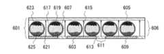
図6は、図1に示した画素部の断面図であり、3画素分を示している。また、表示素子として、マイクロカプセル型電気泳動方式を用いる例を示している。 FIG. 6 is a cross-sectional view of the pixel portion shown in FIG. 1 and shows three pixels. In addition, an example in which a microcapsule electrophoresis method is used as a display element is shown.
一の画素は、画素電極603、対向電極605、画素電極603と対向電極605との間に設けられた帯電層606(帯電物質を有する層とも呼ぶ)を有する表示素子601を有している。また、一の画素に隣接する画素は、画素電極603に隣接する画素電極609、対向電極605、及び帯電層606を有する表示素子601を有している。 One pixel includes a
帯電層606は、複数のマイクロカプセル607を有する。そして、マイクロカプセル607は、着色された粒子623、625を有している。粒子623、625は帯電物質として機能する。 The
そして、画素電極603と画素電極609との間には、隙間611が形成されている。 A
画素電極603、609では、図1乃至図5のような画素電極の構造を用いている。そのため、図6の隙間611において紙面の奥行き方向を見ると、画素電極603が突出した部分613を有している。この突出した部分613は、図1の部分103又は図2の凸部213等に該当する。 The
この状態で画素電極603、609と対向電極605との間に電圧を印加すると、矢印615のように電界が発生する。 When a voltage is applied between the
そして、画素電極603における突出した部分613にも電界が発生するため、隙間611の一部または全部においても、粒子623、625に正しく電界を印加することができる。そのため、図13のような従来例において、隙間5005で生じていた残像を低減することができる。 Since an electric field is generated also in the protruding
なお、上記の隙間611の間隔は、画素電極603と対向電極605との隙間(セルギャップとも呼ぶ)より狭いことが好ましい。 Note that the
以下に、帯電層606の一例について詳細に説明する。 Hereinafter, an example of the
帯電層606は、複数のマイクロカプセル607と、樹脂617とを有する。マイクロカプセル607は、樹脂617中で分散して固定されている。樹脂617は、バインダとしての機能を有する。 The
樹脂617は、透光性を有するとよい。樹脂617の代わりに、空気又は不活性ガスなどの気体を充填してもよい。その場合、画素電極603と対向電極605との一方又は両方に、粘着剤又は接着剤等を含む層を形成して、マイクロカプセル607を固定するとよい。 The
マイクロカプセル607は、膜619と、液体621と、粒子623と、粒子625とを有する。液体621、粒子623と、粒子625とは、膜619の中に封入されている。膜619は、透光性を有する。なお、マイクロカプセル607の断面形状は、円形に限定されず、楕円形や、凹凸を有する形状であってもよい。 The
液体621は、分散液としての機能を有する。液体621により、粒子623及び粒子625を膜619内に分散させることができる。なお、液体621は、透光性を有し、無着色であることが好ましい。 The liquid 621 has a function as a dispersion. With the liquid 621, the
粒子623と粒子625とは、互いに異なる色とする。例えば、一方は黒色であり、他方は白色であるとよい。なお、粒子623と粒子625とは、互いの電荷密度が異なるように帯電されており、帯電物質として機能する。例えば、一方は正に帯電され、他方は負に帯電されるとよい。これにより、画素電極603と対向電極605との間に電位差が生じると、粒子623と粒子625とは、電界方向に応じて移動する。こうして、表示素子601の反射率が変化することにより、階調を制御することができる。 The
なお、マイクロカプセル607の構造は、上記に限定されない。例えば、液体621は、着色されていてもよい。また、粒子の色は、白色及び黒色だけでなく、赤色、緑色、青色、シアン、マゼンタ、イエロー、エメラルドグリーン、朱色などの中から選択することが可能である。また、粒子の色の種類は、1種類であっても、3種類以上であってもよい。 Note that the structure of the
また、表示素子601は、マイクロカプセル型に限定されず、マイクロカップ型、水平移動型、垂直移動型、ツイストボール型(球状又は円筒状等)、粉体移動型、電子粉流体(登録商標)型、帯電トナー、エレクトロウェッティング方式、エレクトロクロミズム方式、又はエレクトロデポジション方式などを適用することができる。帯電層606が有する粒子等の帯電物質の移動により、表示を行うことが可能な素子全般を指す。 Further, the
なお、対向電極605側から表示画面を閲覧する場合、対向電極605は透光性を有する材料で形成する。透光性を有する材料としては、例えば、インジウム錫酸化物(ITO)、酸化珪素を含むインジウム錫酸化物(ITSO)、有機インジウム、有機スズ、酸化亜鉛(ZnO)、インジウム亜鉛酸化物(IZO)、ガリウムを含む酸化亜鉛、酸化スズ(SnO2)、酸化タングステンを含むインジウム酸化物、酸化タングステンを含むインジウム亜鉛酸化物、酸化チタンを含むインジウム酸化物、酸化チタンを含むインジウム錫酸化物などを用いることができる。Note that when the display screen is viewed from the
この場合、画素電極603は、上記の透光性を有する材料、又は、金属材料を用いることができる。特に、可視光に対して反射率が低い金属材料、又は可視光に対して吸収率が高い金属材料を用いて形成することが好ましい。そうすることで、画素電極603での反射が生じにくくなるため、表示画面に対する視認度が向上する。反射率が低い金属としては、例えばクロム等を用いることができる。 In this case, the
また、画素電極603側から表示画面を閲覧してもよく、その場合、画素電極603は上記の透光性を有する材料で形成する。 Further, the display screen may be viewed from the
この場合、対向電極605は、画素電極603より反射率が低い金属を用いて形成することが好ましい。上記の反射率の低い金属を用いることができる。 In this case, the
また、対向電極605側及び画素電極603側の両方から表示画面を閲覧してもよく、その場合、対向電極605及び画素電極603はともに、上記の透光性を有する材料で形成する。そして、反対側への光の透過を防止するため、対向電極605側及び画素電極603側に偏光板をクロスニコルに配置することが好ましい。 Further, the display screen may be viewed from both the
本実施の形態は、他の実施の形態と適宜組み合わせて実施することができる。 This embodiment can be implemented in appropriate combination with any of the other embodiments.
(実施の形態2)
本実施の形態では、画素電極の構造として、図1と異なる一例を示す。(Embodiment 2)
In this embodiment, an example different from that in FIG. 1 is shown as the structure of the pixel electrode.
図7(A)乃至(D)は、表示装置の画素部の上面図である。なお、図7(A)乃至(D)では画素部の一部を示している。 7A to 7D are top views of the pixel portion of the display device. 7A to 7D illustrate part of the pixel portion.
図7(A)では、画素部は画素電極701を有している。画素電極701の端部は、端面方向に、長方形状の突出した部分を有している。 In FIG. 7A, the pixel portion includes a
図7(B)では、画素部は画素電極703を有している。画素電極703の端部は、端面方向に、台形状の突出した部分を有している。 In FIG. 7B, the pixel portion includes a
図7(C)では、画素部は画素電極705を有している。画素電極705の端部は、端面方向に、三角形状の突出した部分を有している。 In FIG. 7C, the pixel portion includes a
図7(D)では、画素部は画素電極707を有している。画素電極707の右辺の端部は、端面方向に、三角形状の突出した部分を有している。更に画素電極707の上辺の端部は端面方向に、突出した部分を有している。 In FIG. 7D, the pixel portion includes a
そして、図7(A)乃至図7(D)の構造とした場合においても、実施の形態1で示した条件1乃至条件4のいずれかを満たすことで、図1乃至図6と同様に、隣接する2つの画素電極間の隙間において電界を印加することができる。そのため、隙間における残像を低減することができる。 Even in the case of the structure shown in FIGS. 7A to 7D, by satisfying any one of the conditions 1 to 4 shown in Embodiment Mode 1, as in FIGS. An electric field can be applied in a gap between two adjacent pixel electrodes. Therefore, the afterimage in the gap can be reduced.
また、図1、図7(A)、図7(B)、図7(C)、及び図7(D)の構造のうち複数を組み合わせてもよい。 In addition, a plurality of the structures shown in FIGS. 1, 7A, 7B, 7C, and 7D may be combined.
本実施の形態は、他の実施の形態と適宜組み合わせて実施することができる。 This embodiment can be implemented in appropriate combination with any of the other embodiments.
(実施の形態3)
本実施の形態では、表示装置の構造の一例を説明する。(Embodiment 3)
In this embodiment, an example of a structure of a display device is described.
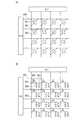
図8は、画素回路及び駆動回路の一例である。図8(A)にパッシブマトリクス型の表示装置、図8(B)にアクティブマトリクス型の表示装置を示す。それぞれマトリクス状に配置された複数の画素801に表示素子601を有する。 FIG. 8 illustrates an example of a pixel circuit and a driver circuit. FIG. 8A illustrates a passive matrix display device, and FIG. 8B illustrates an active matrix display device. Each of the plurality of
表示素子の構造及び駆動方法は、上記実施の形態で示した表示素子の構成を適用することができる。 As the structure and driving method of the display element, the structure of the display element described in any of the above embodiments can be applied.
図8(A)に示すパッシブマトリクス型では、画素801は、複数の交差する配線803、805と、該交差する配線803、805に電気的に接続される表示素子601とを有する。また、配線803は、駆動回路811に電気的に接続され、配線805は、駆動回路813に電気的に接続されている。そして、表示素子601は、駆動回路811及び駆動回路813から入力される電位に応じて、階調表示を行う。 In the passive matrix type illustrated in FIG. 8A, the
また、図8(B)に示すアクティブマトリクス型では、画素801は、複数の交差する配線803、805と、トランジスタ807と、表示素子601と、容量素子809とを有する。そして、トランジスタ807のゲートが配線805に電気的に接続され、ソース又はドレインの一方が配線803に電気的に接続され、ソース又はドレインの他方が表示素子601及び容量素子809に電気的に接続されている。また、配線803は、駆動回路811に電気的に接続され、配線805は駆動回路813に電気的に接続されている。トランジスタ807は、駆動回路813から入力される電位に応じて導通又は非導通が制御される。そして、表示素子601は、トランジスタ807が導通している際に駆動回路811から入力される電位に応じて、階調表示を行う。なお、容量素子809は、表示素子601に印加される電圧を保持する機能を有している。 In the active matrix type illustrated in FIG. 8B, the
次に、画素部の断面構造を示す。 Next, a cross-sectional structure of the pixel portion is shown.
図9(A)はパッシブマトリクス型の断面構造である。基板901と対向基板903との間に表示素子601を有する。そして、基板901側に、画素電極603、609を紙面と垂直方向に延伸して設けることで、図8(A)に示す複数の配線803が形成されている。そのため、画素電極603、609となる複数の配線803の端部において、上記条件1乃至条件3のいずれかを満たしていればよい。一方、対向基板903側には、対向電極605を紙面と平行方向に延伸して設けることで、図8(A)に示す複数の配線805が形成されている。なお、図9(A)では対向電極605は1つしか示していないが、複数の対向電極605が紙面に平行して存在している。すなわち、複数の配線803と複数の配線805が交差する部分に表示素子601が形成されている。 FIG. 9A illustrates a passive matrix cross-sectional structure. A
図9(B)はアクティブマトリクス型の断面構造である。基板901と対向基板903との間に、トランジスタ807及び容量素子809を含む層と、該層上に表示素子601とを有する。そして、トランジスタ807及び容量素子809は、画素電極603と電気的に接続されている。なお、図9(B)では省略しているが、画素電極609にもトランジスタ及び容量素子が電気的に接続されている。 FIG. 9B illustrates an active matrix cross-sectional structure. Between the
基板901及び対向基板903は、ガラス基板、樹脂基板、半導体基板、金属基板、又は、それらに窒化膜又は酸化膜等の絶縁膜を設けたものを適宜用いることができる。 As the
トランジスタ807は、ボトムゲート構造の薄膜トランジスタであり、電極911、絶縁膜913、電極915、電極917、及び半導体層919を有している。ここで、電極911はゲート電極である。また、絶縁膜913はゲート絶縁膜である。そして、電極915又は電極917は、一方がソース電極であり、他方がドレイン電極として機能する。 The
容量素子809は、電極921、電極917、及び絶縁膜913を有している。ここで、電極921は、容量素子809の下部電極であり、電極911(上記ゲート電極)と同層に形成された導電層である。また、絶縁膜913は、上記ゲート絶縁膜と容量素子809の誘電体とを兼ねている。そして、電極917は、絶縁膜913上に延伸して形成された導電層であり、上記ソース電極又はドレイン電極の一方と容量素子809の上部電極とを兼ねている。 The
電極911、電極921、電極915、及び電極917は、モリブデン、チタン、タンタル、タングステン、アルミニウム、銅、ネオジム、スカンジウム等の金属材料又はこれらを主成分とする合金材料を用いて、導電層の単層又は積層により形成されている。 The
絶縁膜913は、酸化珪素膜又は窒化珪素膜等を用いて、単層又は積層で形成されている。 The insulating
半導体層919は、非晶質半導体、多結晶半導体、単結晶半導体、又は微結晶半導体を用いて形成することができる。また、半導体の材料としては、シリコン、ゲルマニウム、有機半導体、又は酸化物半導体等を用いることができる。また、p型トランジスタとしてもよく、n型トランジスタとしてもよい。なお、チャネルエッチ型又はチャネルストップ型としてもよく、トップゲート構造としてもよい。また、薄膜トランジスタとせずに、半導体基板を用いたトランジスタ(バルクトランジスタとも呼ぶ)としてもよい。 The
また、トランジスタ807は、シングルドレイン構造、LDD(低濃度ドレイン)構造、ゲートオーバーラップドレイン構造など各種構造を適用することができる。 The
そして、トランジスタ807及び容量素子809と、画素電極603との間には絶縁膜923が形成されている。 An insulating
絶縁膜923は、酸化珪素若しくは窒化珪素等の無機材料、ポリイミド、ポリアミド、ベンゾシクロブテン、アクリル、若しくはエポキシ等の有機材料、又はシロキサン材料等を用いて、単層又は積層で形成されている。 The insulating
また、基板901側又は対向基板903側に、カラーフィルタ(CF)を設ける構成や、ブラックマトリクス(BM)を設ける構成等を適宜採用してもよい。なお、基板901側及び対向基板903側の両方に、CFやBMを設けてもよい。 Further, a structure in which a color filter (CF) is provided on the
本実施の形態は、他の実施の形態と適宜組み合わせて実施することができる。 This embodiment can be implemented in appropriate combination with any of the other embodiments.
(実施の形態4)
本実施の形態では、表示装置の作製方法の一例を説明する。なお、材料や構造などは、上記実施の形態で示す構成を適宜用いることができる。(Embodiment 4)
In this embodiment, an example of a method for manufacturing a display device will be described. Note that the structures described in the above embodiments can be used as appropriate for materials, structures, and the like.
まず、図9(A)を用いてパッシブマトリクス型の表示装置の作製方法を説明する。 First, a method for manufacturing a passive matrix display device is described with reference to FIG.
基板901上に、紙面と垂直方向に延伸するように、画素電極603、609となる配線を形成する。ここで、画素電極603、609は、該画素電極となる導電膜を成膜した後、エッチング等を施し、上記の条件1乃至条件3のいずれかを満たすように加工する。 Wirings to be
次に、画素電極603、609上に、帯電層606(帯電物質を有する層とも呼ぶ)を形成する。例えば、画素電極603、609上に、マイクロカプセル607が分散されて固定された樹脂617を設ける。 Next, a charged layer 606 (also referred to as a layer having a charged substance) is formed over the
続いて、樹脂617上(帯電層606上)に、紙面と平行方向に延伸するように、対向電極605となる配線を形成する。なお、予め対向電極605が形成された樹脂617を、画素電極603、609上に設けてもよい。 Subsequently, a wiring to be the
次に、対向電極605上に、対向基板903を設ける。対向基板903は、シール材を用いて基板901と貼り合わせる。 Next, a
なお、対向電極605が形成された対向基板903を、シール材を用いて基板901と貼り合わせてもよい。 Note that the
また、マイクロカプセル型の代わりに電子粉流体型とする場合、正に帯電したある色の高分子ポリマー微粒子と、負に帯電した異なる色の高分子ポリマー微粒子を画素電極603と対向電極605の間に設ける構成とすればよい。このように、上述した他の方式を用いて表示素子を構成することもできる。 Further, when an electropowder fluid type is used instead of the microcapsule type, a positively charged polymer polymer fine particle of a certain color and a negatively charged polymer polymer fine particle of a different color are placed between the
以上のようにして、パッシブマトリクス型の表示装置を作製することができる。 As described above, a passive matrix display device can be manufactured.
次に、図9(B)を用いて、アクティブマトリクス型の作製方法の一例を説明する。パッシブマトリクス型と同様の工程については省略する。 Next, an example of a manufacturing method of an active matrix type will be described with reference to FIG. Steps similar to those of the passive matrix type are omitted.
基板901上に、トランジスタ807及び容量素子809を形成する。 A
トランジスタ807及び容量素子809上に絶縁膜923を形成する。 An insulating
絶縁膜923上に画素電極603、609を形成する。ここで、画素電極603、609は、該画素電極となる導電膜を成膜した後、エッチング等を施し、上記の条件1乃至条件4のいずれかを満たすように加工する。
次に、画素電極603、609上に、帯電層606(帯電物質を有する層とも呼ぶ)を形成する。例えば、画素電極603、609上に、マイクロカプセル607が分散されて固定された樹脂617を設ける。 Next, a charged layer 606 (also referred to as a layer having a charged substance) is formed over the
続いて、樹脂617上(帯電層606上)に、対向電極605を形成する。なお、予め対向電極605が形成された樹脂617を、画素電極603、609上に設けてもよい。 Subsequently, a
次に、対向電極605上に、対向基板903を設ける。対向基板903は、シール材を用いて基板901と貼り合わせる。 Next, a
なお、対向電極605が形成された対向基板903を、シール材を用いて基板901と貼り合わせてもよい。 Note that the
以上のようにして、アクティブマトリックス型の表示装置を作製することができる。 As described above, an active matrix display device can be manufactured.
本実施の形態は、他の実施の形態と適宜組み合わせて実施することができる。 This embodiment can be implemented in appropriate combination with any of the other embodiments.
(実施の形態5)
本実施の形態では、表示装置の作製方法について、実施の形態4と異なる一例を示す。なお、材料や構造などは、上記実施の形態で示す構成を適宜用いることができる。(Embodiment 5)
In this embodiment, an example of a method for manufacturing a display device, which is different from that in Embodiment 4, is described. Note that the structures described in the above embodiments can be used as appropriate for materials, structures, and the like.
まず、基板901上に剥離層931を形成する(図10(A)参照)。 First, the
剥離層931は、タングステン、モリブデン、チタン、タンタル、ニオブ、ニッケル、コバルト、ジルコニウム、亜鉛、ルテニウム、ロジウム、パラジウム、オスミウム、イリジウム、珪素等の材料を用いて、単層又は積層させて形成することができる。又は、これらの元素を主成分とする合金材料を用いて形成してもよいし、これらの元素を主成分とする化合物材料を用いて形成してもよい。これらの材料を用いて、スパッタリング法、プラズマCVD法、塗布法、印刷法等により、厚さ30nm〜200nmで剥離層931を形成することができる。 The
また、剥離層931上にバッファ層として機能する絶縁膜(窒化珪素膜又は酸化珪素膜等)を形成してもよい。該絶縁膜を設けることで、後の剥離工程で剥離層931の表面での剥離が容易になる。 Further, an insulating film (such as a silicon nitride film or a silicon oxide film) functioning as a buffer layer may be formed over the
次に、剥離層931上に画素電極603、609を形成する。ここで、画素電極603、609は、該画素電極となる導電膜を成膜した後、エッチング等を施し、上記の条件1乃至条件4のいずれかを満たすように加工する。 Next,
画素電極603、609上に絶縁膜933を形成する。絶縁膜933としては、酸化珪素又は窒化珪素等の無機材料、ポリイミド、ポリアミド、ベンゾシクロブテン、アクリル、又はエポキシ等の有機材料、シロキサン材料等を用いて、単層又は積層で形成する。これらの材料を用いて、CVD法、スパッタ法、SOG法、液滴吐出法、スクリーン印刷法等により絶縁膜933を形成することができる。 An insulating
そして、絶縁膜933上にトランジスタ807及び容量素子809を形成する。また、トランジスタ807及び容量素子809と、画素電極603とを電気的に接続する。なお、図10(A)では、画素電極609に電気的に接続されるトランジスタ及び容量素子は省略している。 Then, a
次に、基板901の端部に設けられた絶縁膜933の一部をエッチング等により除去した後、トランジスタ807及び容量素子809を覆って絶縁膜935を形成する。絶縁膜935は、バリア層として機能し、窒素含有層(窒化珪素、窒化酸化珪素、酸化窒化珪素等を含む層)を用いて形成することができる。 Next, after part of the insulating
次に、絶縁膜935にレーザー光を照射して溝937を形成する(図10(B)参照)。そして、少なくとも溝937を覆うように、セパレートフィルム939を設ける(図10(C)参照)。 Next, the insulating
次に、絶縁膜935上に、第1の有機樹脂941を形成する。セパレートフィルム939を設けることで、第1の有機樹脂941が溝937に侵入して剥離層931と接着することを防止できる。なお、第1の有機樹脂941は、基板(支持基板とも呼ぶ)として機能する。 Next, a first
続いて、溝937をきっかけとして、剥離層931の表面において、素子層943を基板901から剥離する(図10(D)参照)。そして、剥離後にセパレートフィルム939を取り除く。 Subsequently, the
次に、画素電極603、609上に、他の実施の形態で示したように、帯電層606(帯電物質を有する層とも呼ぶ)を形成する(図10(E)参照)。なお、剥離した素子層943の上下を反転させて用いている。 Next, a charged layer 606 (also referred to as a layer having a charged substance) is formed over the
そして、帯電層606上に、対向電極605が形成された第2の有機樹脂945を設ける。そして、加熱処理を行い、第1の有機樹脂941と第2の有機樹脂945とを接着させる。第2の有機樹脂945は、対向基板として機能する。 Then, a second
なお、帯電層606、対向電極605、及び対向基板の形成順序は、上記実施の形態と同様に行ってもよい。 Note that the
上記第1の有機樹脂941及び第2の有機樹脂945は、エポキシ樹脂、不飽和ポリエステル樹脂、ポリイミド樹脂、ビスマレイミドトリアジン樹脂又はシアネート樹脂等の熱硬化性樹脂を用いることができる。他にも、ポリフェニレンオキシド樹脂、ポリエーテルイミド樹脂又はフッ素樹脂等の熱可塑性樹脂を用いてもよい。有機樹脂を用いることで、可撓性を有する表示装置を作製することができる。 As the first
なお、以上の作製方法を応用して、パッシブマトリクス型の表示装置を作製することもできる。 Note that a passive matrix display device can be manufactured by applying the above manufacturing method.
本実施の形態は、他の実施の形態と適宜組み合わせて実施することができる。 This embodiment can be implemented in appropriate combination with any of the other embodiments.
(実施の形態6)
本実施の形態では、画素電極と他の配線との位置関係について説明する。(Embodiment 6)
In this embodiment mode, a positional relationship between the pixel electrode and another wiring is described.
図11は、図1乃至図6で示した画素電極と、図8(B)で示した配線803、805との位置関係の一例である。 FIG. 11 illustrates an example of a positional relationship between the pixel electrode illustrated in FIGS. 1 to 6 and the
図11では、画素電極201と配線803、805とが重なっている。すなわち、配線803は隙間950と重ならず、配線805は隙間960と重ならない位置関係にある。 In FIG. 11, the
このような位置関係にすることで、隙間950において、配線803の電位に起因する電界が帯電物質に加わることを防止できる。そのため、隙間950において残像を低減できる。 With this positional relationship, an electric field due to the potential of the
同様に、隙間960において、配線805の電位に起因する電界が帯電物質に加わることを防止できる。そのため、隙間960において残像を低減できる。 Similarly, in the
本実施の形態は、他の実施の形態と適宜組み合わせて実施することができる。 This embodiment can be implemented in appropriate combination with any of the other embodiments.
(実施の形態7)
本実施の形態では、電子機器の一例を説明する。(Embodiment 7)
In this embodiment, an example of an electronic device is described.
図12(A)及び図12(B)は、電子ペーパー(電子書籍、電子ブック等ともいう)である。それぞれ本体4001の表示部4101及び本体4002の表示部4102に、本明細書で開示した表示装置を適用することができる。 12A and 12B illustrate electronic paper (also referred to as an electronic book, an electronic book, or the like). The display device disclosed in this specification can be applied to the
また、電子ペーパーに限らず、図12(C)のテレビ、図12(D)の携帯電話、図12(E)のパーナルコンピュータ、又は図12(F)のゲーム機器等の電子機器において、本体4003〜4006の表示部4103〜4106に、本明細書で開示した表示装置を適用することができる。 In addition to electronic paper, electronic devices such as the television in FIG. 12C, the mobile phone in FIG. 12D, the personal computer in FIG. 12E, or the game device in FIG. The display device disclosed in this specification can be applied to the
本実施の形態は、他の実施の形態と適宜組み合わせて実施することができる。 This embodiment can be implemented in appropriate combination with any of the other embodiments.
101 画素電極
103 部分
104 部分
105 部分
211 凹部
215 凹部
213 凸部
217 凸部
201 画素電極
203 画素電極
205 画素電極
219 隙間
221 隙間
301 部分
303 部分
305 部分
307 頂点
401 端部
403 端部
501 端部
502 端部
503 端部
504 端部
505 部分
507 部分
601 表示素子
603 画素電極
605 対向電極
606 帯電層
607 マイクロカプセル
609 画素電極
611 隙間
613 部分
615 矢印
617 樹脂
619 膜
621 液体
623 粒子
625 粒子
701 画素電極
703 画素電極
705 画素電極
707 画素電極
801 画素
803 配線
805 配線
807 トランジスタ
809 容量素子
811 駆動回路
813 駆動回路
901 基板
903 対向基板
911 電極
915 電極
917 電極
921 電極
913 絶縁膜
923 絶縁膜
919 半導体層
931 剥離層
933 絶縁膜
935 絶縁膜
937 溝
939 セパレートフィルム
941 第1の有機樹脂
943 素子層
945 第2の有機樹脂
950 隙間
960 隙間
4001〜4006 本体
4101〜4106 表示部
5001 画素電極
5003 端部
5005 隙間101
Claims (1)
Translated fromJapanese前記複数の画素電極のうち隣接する2つの画素電極の間には、隙間が形成されており、
前記隙間は、前記画素電極の一辺に渡り間隔が等しくなるように設けられており、
前記隣接する2つの画素電極のうちの一方は、端面方向に台形状に突出する部分を有し、
前記帯電層に電界を印加して表示を行う機能を有することを特徴とする表示装置。A plurality of pixel electrodes and a charged layer above the pixel electrodes;
A gap is formed between two adjacent pixel electrodes among the plurality of pixel electrodes,
The gap is provided so that the interval is equal across one side of the pixel electrode,
One of the two adjacent pixel electrodes has a portion protruding in a trapezoidal shape in the end surface direction,
A display device having a function of performing display by applying an electric field to the charging layer.
Priority Applications (1)
| Application Number | Priority Date | Filing Date | Title |
|---|---|---|---|
| JP2011136107AJP6126775B2 (en) | 2010-06-25 | 2011-06-20 | Display device |
Applications Claiming Priority (3)
| Application Number | Priority Date | Filing Date | Title |
|---|---|---|---|
| JP2010144911 | 2010-06-25 | ||
| JP2010144911 | 2010-06-25 | ||
| JP2011136107AJP6126775B2 (en) | 2010-06-25 | 2011-06-20 | Display device |
Related Child Applications (1)
| Application Number | Title | Priority Date | Filing Date |
|---|---|---|---|
| JP2015213778ADivisionJP2016014907A (en) | 2010-06-25 | 2015-10-30 | Method of producing display device |
Publications (3)
| Publication Number | Publication Date |
|---|---|
| JP2012027456A JP2012027456A (en) | 2012-02-09 |
| JP2012027456A5 JP2012027456A5 (en) | 2014-07-31 |
| JP6126775B2true JP6126775B2 (en) | 2017-05-10 |
Family
ID=45352319
Family Applications (8)
| Application Number | Title | Priority Date | Filing Date |
|---|---|---|---|
| JP2011136107AActiveJP6126775B2 (en) | 2010-06-25 | 2011-06-20 | Display device |
| JP2015213778AWithdrawnJP2016014907A (en) | 2010-06-25 | 2015-10-30 | Method of producing display device |
| JP2017168253AActiveJP6460606B2 (en) | 2010-06-25 | 2017-09-01 | Display device |
| JP2018240426AActiveJP6797887B2 (en) | 2010-06-25 | 2018-12-24 | Display device |
| JP2020191420AActiveJP7142076B2 (en) | 2010-06-25 | 2020-11-18 | Display device |
| JP2022144509AActiveJP7266741B2 (en) | 2010-06-25 | 2022-09-12 | Display device |
| JP2023067834AActiveJP7478284B2 (en) | 2010-06-25 | 2023-04-18 | Display device |
| JP2024068240AActiveJP7737503B2 (en) | 2010-06-25 | 2024-04-19 | display device |
Family Applications After (7)
| Application Number | Title | Priority Date | Filing Date |
|---|---|---|---|
| JP2015213778AWithdrawnJP2016014907A (en) | 2010-06-25 | 2015-10-30 | Method of producing display device |
| JP2017168253AActiveJP6460606B2 (en) | 2010-06-25 | 2017-09-01 | Display device |
| JP2018240426AActiveJP6797887B2 (en) | 2010-06-25 | 2018-12-24 | Display device |
| JP2020191420AActiveJP7142076B2 (en) | 2010-06-25 | 2020-11-18 | Display device |
| JP2022144509AActiveJP7266741B2 (en) | 2010-06-25 | 2022-09-12 | Display device |
| JP2023067834AActiveJP7478284B2 (en) | 2010-06-25 | 2023-04-18 | Display device |
| JP2024068240AActiveJP7737503B2 (en) | 2010-06-25 | 2024-04-19 | display device |
Country Status (3)
| Country | Link |
|---|---|
| US (6) | US8786934B2 (en) |
| JP (8) | JP6126775B2 (en) |
| TW (7) | TWI742766B (en) |
Families Citing this family (6)
| Publication number | Priority date | Publication date | Assignee | Title |
|---|---|---|---|---|
| JP6126775B2 (en)* | 2010-06-25 | 2017-05-10 | 株式会社半導体エネルギー研究所 | Display device |
| KR102491853B1 (en)* | 2015-12-09 | 2023-01-26 | 삼성전자주식회사 | Directional backlight unit and 3D image display apparatus having the same |
| WO2017184816A1 (en)* | 2016-04-22 | 2017-10-26 | E Ink Corporation | Foldable electro-optic display apparatus |
| CN109581769A (en)* | 2018-12-11 | 2019-04-05 | 合肥鑫晟光电科技有限公司 | Dot structure, array substrate and display panel |
| JP2021044278A (en)* | 2019-09-06 | 2021-03-18 | キオクシア株式会社 | Semiconductor device |
| CN112037679A (en)* | 2020-08-12 | 2020-12-04 | 北京纳米能源与系统研究所 | Electronic drawing board and display method |
Family Cites Families (67)
| Publication number | Priority date | Publication date | Assignee | Title |
|---|---|---|---|---|
| JP3096202B2 (en) | 1994-01-31 | 2000-10-10 | ポリプラスチックス株式会社 | Method for producing trioxane |
| JP3774855B2 (en) | 1997-04-25 | 2006-05-17 | 大林精工株式会社 | Liquid crystal display device and manufacturing method. |
| TW509808B (en) | 1997-06-12 | 2002-11-11 | Sharp Kk | Liquid crystal display device |
| JPH11174481A (en)* | 1997-12-05 | 1999-07-02 | San Operation Service:Kk | Display device |
| JPH11174453A (en)* | 1997-12-16 | 1999-07-02 | Fujitsu Ltd | Liquid crystal display |
| US6630977B1 (en) | 1999-05-20 | 2003-10-07 | Semiconductor Energy Laboratory Co., Ltd. | Semiconductor device with capacitor formed around contact hole |
| JP3982137B2 (en)* | 2000-02-09 | 2007-09-26 | セイコーエプソン株式会社 | Electro-optical device and projection display device |
| TW583425B (en) | 2001-08-02 | 2004-04-11 | Sanyo Electric Co | Liquid crystal display |
| JP4785300B2 (en) | 2001-09-07 | 2011-10-05 | 株式会社半導体エネルギー研究所 | Electrophoretic display device, display device, and electronic device |
| JP2003149674A (en) | 2001-11-13 | 2003-05-21 | Hitachi Ltd | Liquid crystal display |
| US6885146B2 (en) | 2002-03-14 | 2005-04-26 | Semiconductor Energy Laboratory Co., Ltd. | Display device comprising substrates, contrast medium and barrier layers between contrast medium and each of substrates |
| TWI240842B (en)* | 2002-04-24 | 2005-10-01 | Sipix Imaging Inc | Matrix driven electrophoretic display with multilayer back plane |
| US7190008B2 (en) | 2002-04-24 | 2007-03-13 | E Ink Corporation | Electro-optic displays, and components for use therein |
| US7116318B2 (en) | 2002-04-24 | 2006-10-03 | E Ink Corporation | Backplanes for display applications, and components for use therein |
| TW588182B (en) | 2002-06-07 | 2004-05-21 | Hannstar Display Corp | Pixel electrode for a liquid crystal display with a high aperture ratio |
| US6911132B2 (en) | 2002-09-24 | 2005-06-28 | Duke University | Apparatus for manipulating droplets by electrowetting-based techniques |
| KR101099927B1 (en) | 2003-05-20 | 2011-12-28 | 이데미쓰 고산 가부시키가이샤 | Amorphous transparent conductive film, raw material sputtering target, amorphous transparent electrode substrate, manufacturing method thereof, and color filter for display |
| KR20050014414A (en) | 2003-07-31 | 2005-02-07 | 삼성전자주식회사 | Multi-domain liquid crystal display including the same |
| KR101100874B1 (en)* | 2003-10-08 | 2012-01-02 | 삼성전자주식회사 | Thin film transistor array panel |
| WO2005045509A2 (en) | 2003-10-27 | 2005-05-19 | E Ink Corporation | Electro-optic displays |
| CN100451784C (en)* | 2004-01-29 | 2009-01-14 | 夏普株式会社 | Display device |
| WO2005090520A1 (en)* | 2004-03-19 | 2005-09-29 | Japan Science And Technology Agency | Liquid crystal display device |
| US7573551B2 (en) | 2004-05-21 | 2009-08-11 | Sanyo Electric Co., Ltd. | Transflective liquid crystal display device and color liquid crystal display device |
| TWI349139B (en)* | 2004-11-30 | 2011-09-21 | Sanyo Electric Co | Liquid crystal display device |
| JP4748440B2 (en)* | 2005-03-03 | 2011-08-17 | セイコーエプソン株式会社 | Electrophoretic display device and electronic apparatus |
| JP2006259383A (en)* | 2005-03-17 | 2006-09-28 | Seiko Epson Corp | Manufacturing method of substrate for electronic device, substrate for electronic device, electronic device and electronic apparatus |
| TWM274548U (en)* | 2005-03-18 | 2005-09-01 | Innolux Display Corp | Liquid crystal display device |
| JP4419944B2 (en) | 2005-03-29 | 2010-02-24 | セイコーエプソン株式会社 | Electrophoretic display device and driving method thereof |
| KR101201017B1 (en) | 2005-06-27 | 2012-11-13 | 엘지디스플레이 주식회사 | Liquid crystal display and fabricating method thereof |
| JP2007010824A (en)* | 2005-06-29 | 2007-01-18 | Mitsubishi Electric Corp | Liquid crystal display panel and pixel defect correcting method thereof |
| KR101225440B1 (en) | 2005-06-30 | 2013-01-25 | 엘지디스플레이 주식회사 | Liquid crystal display and fabricating method thereof |
| JP4746933B2 (en)* | 2005-08-01 | 2011-08-10 | Nec液晶テクノロジー株式会社 | Color electronic paper display device |
| TWI442151B (en) | 2005-10-18 | 2014-06-21 | Semiconductor Energy Lab | Liquid crystal display device |
| JP2007133013A (en)* | 2005-11-08 | 2007-05-31 | Canon Inc | Particle movement type display device |
| JP4442580B2 (en) | 2006-03-28 | 2010-03-31 | ソニー株式会社 | Optical element and imaging device |
| US7847904B2 (en) | 2006-06-02 | 2010-12-07 | Semiconductor Energy Laboratory Co., Ltd. | Liquid crystal display device and electronic appliance |
| JP2008058690A (en)* | 2006-08-31 | 2008-03-13 | Seiko Epson Corp | Liquid crystal device and electronic device |
| CN103257491B (en) | 2006-09-29 | 2017-04-19 | 株式会社半导体能源研究所 | Semiconductor device |
| US8223287B2 (en)* | 2006-10-11 | 2012-07-17 | Seiko Epson Corporation | Electrooptic device and electronic device |
| JP2008096616A (en)* | 2006-10-11 | 2008-04-24 | Seiko Epson Corp | Electro-optical device and electronic apparatus |
| US8531991B2 (en)* | 2006-10-16 | 2013-09-10 | Cisco Technology, Inc. | Multi-chassis emulated switch |
| JP5119645B2 (en)* | 2006-10-20 | 2013-01-16 | セイコーエプソン株式会社 | Electro-optical device and electronic apparatus including the same |
| KR20080051273A (en)* | 2006-12-05 | 2008-06-11 | 삼성전자주식회사 | Electrophoretic display device and manufacturing method thereof |
| JP2008159934A (en)* | 2006-12-25 | 2008-07-10 | Kyodo Printing Co Ltd | Flexible TFT substrate, manufacturing method thereof and flexible display |
| JP5075420B2 (en) | 2007-02-09 | 2012-11-21 | 株式会社東芝 | Liquid crystal display |
| JP2008292997A (en) | 2007-04-27 | 2008-12-04 | Semiconductor Energy Lab Co Ltd | Method for manufacturing liquid crystal display device |
| TWI431386B (en) | 2007-05-01 | 2014-03-21 | Prime View Int Co Ltd | An electronic-ink display panel |
| JP2009003437A (en) | 2007-05-18 | 2009-01-08 | Semiconductor Energy Lab Co Ltd | Liquid crystal display and manufacturing method therefor |
| JP5218959B2 (en) | 2007-06-01 | 2013-06-26 | 株式会社リコー | Electrophoretic display device, display method, method for manufacturing electrophoretic display element, and method for manufacturing electrophoretic display device |
| JP2009076852A (en) | 2007-08-31 | 2009-04-09 | Seiko Epson Corp | Thin film element, thin film element manufacturing method, and display device |
| US7968388B2 (en) | 2007-08-31 | 2011-06-28 | Seiko Epson Corporation | Thin-film device, method for manufacturing thin-film device, and display |
| KR101346921B1 (en) | 2008-02-19 | 2014-01-02 | 엘지디스플레이 주식회사 | A flat display device and method of manufacturing the same |
| KR101445332B1 (en)* | 2008-02-19 | 2014-10-01 | 삼성디스플레이 주식회사 | Display device |
| JP5540517B2 (en)* | 2008-02-22 | 2014-07-02 | 凸版印刷株式会社 | Image display device |
| JP5266815B2 (en)* | 2008-03-14 | 2013-08-21 | セイコーエプソン株式会社 | Electrophoretic display device and electronic apparatus |
| JP5358324B2 (en)* | 2008-07-10 | 2013-12-04 | 株式会社半導体エネルギー研究所 | Electronic paper |
| JP5376287B2 (en) | 2008-08-06 | 2013-12-25 | セイコーエプソン株式会社 | Circuit board, electro-optical device, electronic equipment |
| TW201023021A (en)* | 2008-12-03 | 2010-06-16 | Chi Hsin Electronics Corp | Touch sensitive electronic paper display apparatus |
| KR101283366B1 (en) | 2008-12-23 | 2013-07-08 | 엘지디스플레이 주식회사 | An Electrophoretic display device and method of fabricating the same |
| KR101711678B1 (en) | 2009-05-02 | 2017-03-02 | 가부시키가이샤 한도오따이 에네루기 켄큐쇼 | Electronic device |
| KR101857405B1 (en) | 2009-07-10 | 2018-05-11 | 가부시키가이샤 한도오따이 에네루기 켄큐쇼 | Semiconductor device and method for manufacturing the same |
| WO2011010545A1 (en) | 2009-07-18 | 2011-01-27 | Semiconductor Energy Laboratory Co., Ltd. | Semiconductor device and method for manufacturing the same |
| KR101904811B1 (en) | 2009-07-24 | 2018-10-05 | 가부시키가이샤 한도오따이 에네루기 켄큐쇼 | Semiconductor device |
| JP4930561B2 (en) | 2009-09-07 | 2012-05-16 | カシオ計算機株式会社 | Electrophoretic display panel |
| TWI528342B (en) | 2009-09-16 | 2016-04-01 | 半導體能源研究所股份有限公司 | Display device and driving method thereof |
| JP6126775B2 (en)* | 2010-06-25 | 2017-05-10 | 株式会社半導体エネルギー研究所 | Display device |
| JP5947000B2 (en)* | 2010-07-01 | 2016-07-06 | 株式会社半導体エネルギー研究所 | Electric field drive type display device |
- 2011
- 2011-06-20JPJP2011136107Apatent/JP6126775B2/enactiveActive
- 2011-06-21TWTW109124242Apatent/TWI742766B/enactive
- 2011-06-21TWTW107121155Apatent/TWI701491B/enactive
- 2011-06-21TWTW110135318Apatent/TWI802020B/enactive
- 2011-06-21TWTW104134020Apatent/TWI567470B/enactive
- 2011-06-21TWTW100121639Apatent/TWI515500B/enactive
- 2011-06-21TWTW106118888Apatent/TWI635346B/enactive
- 2011-06-21TWTW105134061Apatent/TWI596415B/enactive
- 2011-06-24USUS13/168,025patent/US8786934B2/enactiveActive
- 2014
- 2014-07-18USUS14/335,306patent/US8958140B2/enactiveActive
- 2015
- 2015-02-10USUS14/618,418patent/US9268193B2/enactiveActive
- 2015-10-30JPJP2015213778Apatent/JP2016014907A/ennot_activeWithdrawn
- 2016
- 2016-02-17USUS15/046,207patent/US9488895B2/enactiveActive
- 2016-11-02USUS15/341,874patent/US9857658B2/enactiveActive
- 2017
- 2017-09-01JPJP2017168253Apatent/JP6460606B2/enactiveActive
- 2017-12-27USUS15/855,167patent/US10185201B2/enactiveActive
- 2018
- 2018-12-24JPJP2018240426Apatent/JP6797887B2/enactiveActive
- 2020
- 2020-11-18JPJP2020191420Apatent/JP7142076B2/enactiveActive
- 2022
- 2022-09-12JPJP2022144509Apatent/JP7266741B2/enactiveActive
- 2023
- 2023-04-18JPJP2023067834Apatent/JP7478284B2/enactiveActive
- 2024
- 2024-04-19JPJP2024068240Apatent/JP7737503B2/enactiveActive
Also Published As
Similar Documents
| Publication | Publication Date | Title |
|---|---|---|
| JP6460606B2 (en) | Display device | |
| KR101993592B1 (en) | Display device | |
| KR20140006326A (en) | Electrophoretic display device and manufacturing method thereof |
Legal Events
| Date | Code | Title | Description |
|---|---|---|---|
| A521 | Request for written amendment filed | Free format text:JAPANESE INTERMEDIATE CODE: A523 Effective date:20140617 | |
| A621 | Written request for application examination | Free format text:JAPANESE INTERMEDIATE CODE: A621 Effective date:20140617 | |
| A131 | Notification of reasons for refusal | Free format text:JAPANESE INTERMEDIATE CODE: A131 Effective date:20150519 | |
| A521 | Request for written amendment filed | Free format text:JAPANESE INTERMEDIATE CODE: A523 Effective date:20150617 | |
| A02 | Decision of refusal | Free format text:JAPANESE INTERMEDIATE CODE: A02 Effective date:20150818 | |
| A521 | Request for written amendment filed | Free format text:JAPANESE INTERMEDIATE CODE: A523 Effective date:20151030 | |
| A911 | Transfer to examiner for re-examination before appeal (zenchi) | Free format text:JAPANESE INTERMEDIATE CODE: A911 Effective date:20151109 | |
| A912 | Re-examination (zenchi) completed and case transferred to appeal board | Free format text:JAPANESE INTERMEDIATE CODE: A912 Effective date:20151218 | |
| A61 | First payment of annual fees (during grant procedure) | Free format text:JAPANESE INTERMEDIATE CODE: A61 Effective date:20170410 | |
| R150 | Certificate of patent or registration of utility model | Ref document number:6126775 Country of ref document:JP Free format text:JAPANESE INTERMEDIATE CODE: R150 | |
| R250 | Receipt of annual fees | Free format text:JAPANESE INTERMEDIATE CODE: R250 | |
| R250 | Receipt of annual fees | Free format text:JAPANESE INTERMEDIATE CODE: R250 | |
| R250 | Receipt of annual fees | Free format text:JAPANESE INTERMEDIATE CODE: R250 | |
| R250 | Receipt of annual fees | Free format text:JAPANESE INTERMEDIATE CODE: R250 | |
| R250 | Receipt of annual fees | Free format text:JAPANESE INTERMEDIATE CODE: R250 | |
| R250 | Receipt of annual fees | Free format text:JAPANESE INTERMEDIATE CODE: R250 |