JP6114668B2 - Substrate processing apparatus and substrate processing method - Google Patents
Substrate processing apparatus and substrate processing methodDownload PDFInfo
- Publication number
- JP6114668B2 JP6114668B2JP2013193412AJP2013193412AJP6114668B2JP 6114668 B2JP6114668 B2JP 6114668B2JP 2013193412 AJP2013193412 AJP 2013193412AJP 2013193412 AJP2013193412 AJP 2013193412AJP 6114668 B2JP6114668 B2JP 6114668B2
- Authority
- JP
- Japan
- Prior art keywords
- substrate
- recess
- wafer
- reaction gas
- substrate processing
- Prior art date
- Legal status (The legal status is an assumption and is not a legal conclusion. Google has not performed a legal analysis and makes no representation as to the accuracy of the status listed.)
- Active
Links
- 239000000758substrateSubstances0.000titleclaimsdescription122
- 238000012545processingMethods0.000titleclaimsdescription54
- 238000003672processing methodMethods0.000titleclaimsdescription18
- 239000007789gasSubstances0.000claimsdescription64
- 238000000926separation methodMethods0.000claimsdescription44
- 239000012495reaction gasSubstances0.000claimsdescription43
- 230000003028elevating effectEffects0.000claimsdescription42
- 230000007246mechanismEffects0.000claimsdescription17
- 238000006243chemical reactionMethods0.000claimsdescription6
- 239000007795chemical reaction productSubstances0.000claimsdescription2
- 235000012431wafersNutrition0.000description136
- 238000000034methodMethods0.000description32
- 238000012546transferMethods0.000description16
- 230000008569processEffects0.000description15
- 239000002245particleSubstances0.000description13
- 230000002093peripheral effectEffects0.000description13
- 238000011068loading methodMethods0.000description11
- 230000014509gene expressionEffects0.000description8
- 238000010586diagramMethods0.000description6
- 230000001276controlling effectEffects0.000description5
- 238000010926purgeMethods0.000description5
- 230000015572biosynthetic processEffects0.000description4
- 238000010438heat treatmentMethods0.000description4
- 239000004065semiconductorSubstances0.000description4
- 238000000231atomic layer depositionMethods0.000description3
- 239000010453quartzSubstances0.000description3
- VYPSYNLAJGMNEJ-UHFFFAOYSA-Nsilicon dioxideInorganic materialsO=[Si]=OVYPSYNLAJGMNEJ-UHFFFAOYSA-N0.000description3
- 238000003860storageMethods0.000description3
- 230000000052comparative effectEffects0.000description2
- XUIMIQQOPSSXEZ-UHFFFAOYSA-NSiliconChemical compound[Si]XUIMIQQOPSSXEZ-UHFFFAOYSA-N0.000description1
- 238000013459approachMethods0.000description1
- 230000005540biological transmissionEffects0.000description1
- 230000008859changeEffects0.000description1
- 230000000694effectsEffects0.000description1
- 230000006870functionEffects0.000description1
- 208000014674injuryDiseases0.000description1
- 238000002955isolationMethods0.000description1
- 238000004519manufacturing processMethods0.000description1
- 230000000149penetrating effectEffects0.000description1
- 230000001105regulatory effectEffects0.000description1
- 238000012827research and developmentMethods0.000description1
- 230000004044responseEffects0.000description1
- 229910052710siliconInorganic materials0.000description1
- 239000010703siliconSubstances0.000description1
- 230000008733traumaEffects0.000description1
Images


Classifications
- C—CHEMISTRY; METALLURGY
- C23—COATING METALLIC MATERIAL; COATING MATERIAL WITH METALLIC MATERIAL; CHEMICAL SURFACE TREATMENT; DIFFUSION TREATMENT OF METALLIC MATERIAL; COATING BY VACUUM EVAPORATION, BY SPUTTERING, BY ION IMPLANTATION OR BY CHEMICAL VAPOUR DEPOSITION, IN GENERAL; INHIBITING CORROSION OF METALLIC MATERIAL OR INCRUSTATION IN GENERAL
- C23C—COATING METALLIC MATERIAL; COATING MATERIAL WITH METALLIC MATERIAL; SURFACE TREATMENT OF METALLIC MATERIAL BY DIFFUSION INTO THE SURFACE, BY CHEMICAL CONVERSION OR SUBSTITUTION; COATING BY VACUUM EVAPORATION, BY SPUTTERING, BY ION IMPLANTATION OR BY CHEMICAL VAPOUR DEPOSITION, IN GENERAL
- C23C16/00—Chemical coating by decomposition of gaseous compounds, without leaving reaction products of surface material in the coating, i.e. chemical vapour deposition [CVD] processes
- C23C16/44—Chemical coating by decomposition of gaseous compounds, without leaving reaction products of surface material in the coating, i.e. chemical vapour deposition [CVD] processes characterised by the method of coating
- C23C16/458—Chemical coating by decomposition of gaseous compounds, without leaving reaction products of surface material in the coating, i.e. chemical vapour deposition [CVD] processes characterised by the method of coating characterised by the method used for supporting substrates in the reaction chamber
- C23C16/4582—Rigid and flat substrates, e.g. plates or discs
- C23C16/4583—Rigid and flat substrates, e.g. plates or discs the substrate being supported substantially horizontally
- C23C16/4586—Elements in the interior of the support, e.g. electrodes, heating or cooling devices
- H—ELECTRICITY
- H01—ELECTRIC ELEMENTS
- H01L—SEMICONDUCTOR DEVICES NOT COVERED BY CLASS H10
- H01L21/00—Processes or apparatus adapted for the manufacture or treatment of semiconductor or solid state devices or of parts thereof
- H01L21/67—Apparatus specially adapted for handling semiconductor or electric solid state devices during manufacture or treatment thereof; Apparatus specially adapted for handling wafers during manufacture or treatment of semiconductor or electric solid state devices or components ; Apparatus not specifically provided for elsewhere
- H01L21/677—Apparatus specially adapted for handling semiconductor or electric solid state devices during manufacture or treatment thereof; Apparatus specially adapted for handling wafers during manufacture or treatment of semiconductor or electric solid state devices or components ; Apparatus not specifically provided for elsewhere for conveying, e.g. between different workstations
- H01L21/67703—Apparatus specially adapted for handling semiconductor or electric solid state devices during manufacture or treatment thereof; Apparatus specially adapted for handling wafers during manufacture or treatment of semiconductor or electric solid state devices or components ; Apparatus not specifically provided for elsewhere for conveying, e.g. between different workstations between different workstations
- H01L21/67712—Apparatus specially adapted for handling semiconductor or electric solid state devices during manufacture or treatment thereof; Apparatus specially adapted for handling wafers during manufacture or treatment of semiconductor or electric solid state devices or components ; Apparatus not specifically provided for elsewhere for conveying, e.g. between different workstations between different workstations the substrate being handled substantially vertically
- C—CHEMISTRY; METALLURGY
- C23—COATING METALLIC MATERIAL; COATING MATERIAL WITH METALLIC MATERIAL; CHEMICAL SURFACE TREATMENT; DIFFUSION TREATMENT OF METALLIC MATERIAL; COATING BY VACUUM EVAPORATION, BY SPUTTERING, BY ION IMPLANTATION OR BY CHEMICAL VAPOUR DEPOSITION, IN GENERAL; INHIBITING CORROSION OF METALLIC MATERIAL OR INCRUSTATION IN GENERAL
- C23C—COATING METALLIC MATERIAL; COATING MATERIAL WITH METALLIC MATERIAL; SURFACE TREATMENT OF METALLIC MATERIAL BY DIFFUSION INTO THE SURFACE, BY CHEMICAL CONVERSION OR SUBSTITUTION; COATING BY VACUUM EVAPORATION, BY SPUTTERING, BY ION IMPLANTATION OR BY CHEMICAL VAPOUR DEPOSITION, IN GENERAL
- C23C16/00—Chemical coating by decomposition of gaseous compounds, without leaving reaction products of surface material in the coating, i.e. chemical vapour deposition [CVD] processes
- C23C16/44—Chemical coating by decomposition of gaseous compounds, without leaving reaction products of surface material in the coating, i.e. chemical vapour deposition [CVD] processes characterised by the method of coating
- C23C16/455—Chemical coating by decomposition of gaseous compounds, without leaving reaction products of surface material in the coating, i.e. chemical vapour deposition [CVD] processes characterised by the method of coating characterised by the method used for introducing gases into reaction chamber or for modifying gas flows in reaction chamber
- C23C16/45519—Inert gas curtains
- C23C16/45521—Inert gas curtains the gas, other than thermal contact gas, being introduced the rear of the substrate to flow around its periphery
- C—CHEMISTRY; METALLURGY
- C23—COATING METALLIC MATERIAL; COATING MATERIAL WITH METALLIC MATERIAL; CHEMICAL SURFACE TREATMENT; DIFFUSION TREATMENT OF METALLIC MATERIAL; COATING BY VACUUM EVAPORATION, BY SPUTTERING, BY ION IMPLANTATION OR BY CHEMICAL VAPOUR DEPOSITION, IN GENERAL; INHIBITING CORROSION OF METALLIC MATERIAL OR INCRUSTATION IN GENERAL
- C23C—COATING METALLIC MATERIAL; COATING MATERIAL WITH METALLIC MATERIAL; SURFACE TREATMENT OF METALLIC MATERIAL BY DIFFUSION INTO THE SURFACE, BY CHEMICAL CONVERSION OR SUBSTITUTION; COATING BY VACUUM EVAPORATION, BY SPUTTERING, BY ION IMPLANTATION OR BY CHEMICAL VAPOUR DEPOSITION, IN GENERAL
- C23C16/00—Chemical coating by decomposition of gaseous compounds, without leaving reaction products of surface material in the coating, i.e. chemical vapour deposition [CVD] processes
- C23C16/44—Chemical coating by decomposition of gaseous compounds, without leaving reaction products of surface material in the coating, i.e. chemical vapour deposition [CVD] processes characterised by the method of coating
- C23C16/455—Chemical coating by decomposition of gaseous compounds, without leaving reaction products of surface material in the coating, i.e. chemical vapour deposition [CVD] processes characterised by the method of coating characterised by the method used for introducing gases into reaction chamber or for modifying gas flows in reaction chamber
- C23C16/45523—Pulsed gas flow or change of composition over time
- C23C16/45525—Atomic layer deposition [ALD]
- C23C16/45544—Atomic layer deposition [ALD] characterized by the apparatus
- C23C16/45548—Atomic layer deposition [ALD] characterized by the apparatus having arrangements for gas injection at different locations of the reactor for each ALD half-reaction
- C23C16/45551—Atomic layer deposition [ALD] characterized by the apparatus having arrangements for gas injection at different locations of the reactor for each ALD half-reaction for relative movement of the substrate and the gas injectors or half-reaction reactor compartments
- C—CHEMISTRY; METALLURGY
- C23—COATING METALLIC MATERIAL; COATING MATERIAL WITH METALLIC MATERIAL; CHEMICAL SURFACE TREATMENT; DIFFUSION TREATMENT OF METALLIC MATERIAL; COATING BY VACUUM EVAPORATION, BY SPUTTERING, BY ION IMPLANTATION OR BY CHEMICAL VAPOUR DEPOSITION, IN GENERAL; INHIBITING CORROSION OF METALLIC MATERIAL OR INCRUSTATION IN GENERAL
- C23C—COATING METALLIC MATERIAL; COATING MATERIAL WITH METALLIC MATERIAL; SURFACE TREATMENT OF METALLIC MATERIAL BY DIFFUSION INTO THE SURFACE, BY CHEMICAL CONVERSION OR SUBSTITUTION; COATING BY VACUUM EVAPORATION, BY SPUTTERING, BY ION IMPLANTATION OR BY CHEMICAL VAPOUR DEPOSITION, IN GENERAL
- C23C16/00—Chemical coating by decomposition of gaseous compounds, without leaving reaction products of surface material in the coating, i.e. chemical vapour deposition [CVD] processes
- C23C16/44—Chemical coating by decomposition of gaseous compounds, without leaving reaction products of surface material in the coating, i.e. chemical vapour deposition [CVD] processes characterised by the method of coating
- C23C16/458—Chemical coating by decomposition of gaseous compounds, without leaving reaction products of surface material in the coating, i.e. chemical vapour deposition [CVD] processes characterised by the method of coating characterised by the method used for supporting substrates in the reaction chamber
- C23C16/4582—Rigid and flat substrates, e.g. plates or discs
- C23C16/4583—Rigid and flat substrates, e.g. plates or discs the substrate being supported substantially horizontally
- C23C16/4584—Rigid and flat substrates, e.g. plates or discs the substrate being supported substantially horizontally the substrate being rotated
- H—ELECTRICITY
- H01—ELECTRIC ELEMENTS
- H01L—SEMICONDUCTOR DEVICES NOT COVERED BY CLASS H10
- H01L21/00—Processes or apparatus adapted for the manufacture or treatment of semiconductor or solid state devices or of parts thereof
- H01L21/67—Apparatus specially adapted for handling semiconductor or electric solid state devices during manufacture or treatment thereof; Apparatus specially adapted for handling wafers during manufacture or treatment of semiconductor or electric solid state devices or components ; Apparatus not specifically provided for elsewhere
- H01L21/683—Apparatus specially adapted for handling semiconductor or electric solid state devices during manufacture or treatment thereof; Apparatus specially adapted for handling wafers during manufacture or treatment of semiconductor or electric solid state devices or components ; Apparatus not specifically provided for elsewhere for supporting or gripping
- H01L21/687—Apparatus specially adapted for handling semiconductor or electric solid state devices during manufacture or treatment thereof; Apparatus specially adapted for handling wafers during manufacture or treatment of semiconductor or electric solid state devices or components ; Apparatus not specifically provided for elsewhere for supporting or gripping using mechanical means, e.g. chucks, clamps or pinches
- H01L21/68714—Apparatus specially adapted for handling semiconductor or electric solid state devices during manufacture or treatment thereof; Apparatus specially adapted for handling wafers during manufacture or treatment of semiconductor or electric solid state devices or components ; Apparatus not specifically provided for elsewhere for supporting or gripping using mechanical means, e.g. chucks, clamps or pinches the wafers being placed on a susceptor, stage or support
- H01L21/68742—Apparatus specially adapted for handling semiconductor or electric solid state devices during manufacture or treatment thereof; Apparatus specially adapted for handling wafers during manufacture or treatment of semiconductor or electric solid state devices or components ; Apparatus not specifically provided for elsewhere for supporting or gripping using mechanical means, e.g. chucks, clamps or pinches the wafers being placed on a susceptor, stage or support characterised by a lifting arrangement, e.g. lift pins
- H—ELECTRICITY
- H01—ELECTRIC ELEMENTS
- H01L—SEMICONDUCTOR DEVICES NOT COVERED BY CLASS H10
- H01L21/00—Processes or apparatus adapted for the manufacture or treatment of semiconductor or solid state devices or of parts thereof
- H01L21/67—Apparatus specially adapted for handling semiconductor or electric solid state devices during manufacture or treatment thereof; Apparatus specially adapted for handling wafers during manufacture or treatment of semiconductor or electric solid state devices or components ; Apparatus not specifically provided for elsewhere
- H01L21/683—Apparatus specially adapted for handling semiconductor or electric solid state devices during manufacture or treatment thereof; Apparatus specially adapted for handling wafers during manufacture or treatment of semiconductor or electric solid state devices or components ; Apparatus not specifically provided for elsewhere for supporting or gripping
- H01L21/687—Apparatus specially adapted for handling semiconductor or electric solid state devices during manufacture or treatment thereof; Apparatus specially adapted for handling wafers during manufacture or treatment of semiconductor or electric solid state devices or components ; Apparatus not specifically provided for elsewhere for supporting or gripping using mechanical means, e.g. chucks, clamps or pinches
- H01L21/68714—Apparatus specially adapted for handling semiconductor or electric solid state devices during manufacture or treatment thereof; Apparatus specially adapted for handling wafers during manufacture or treatment of semiconductor or electric solid state devices or components ; Apparatus not specifically provided for elsewhere for supporting or gripping using mechanical means, e.g. chucks, clamps or pinches the wafers being placed on a susceptor, stage or support
- H01L21/68764—Apparatus specially adapted for handling semiconductor or electric solid state devices during manufacture or treatment thereof; Apparatus specially adapted for handling wafers during manufacture or treatment of semiconductor or electric solid state devices or components ; Apparatus not specifically provided for elsewhere for supporting or gripping using mechanical means, e.g. chucks, clamps or pinches the wafers being placed on a susceptor, stage or support characterised by a movable susceptor, stage or support, others than those only rotating on their own vertical axis, e.g. susceptors on a rotating caroussel
- H—ELECTRICITY
- H01—ELECTRIC ELEMENTS
- H01L—SEMICONDUCTOR DEVICES NOT COVERED BY CLASS H10
- H01L21/00—Processes or apparatus adapted for the manufacture or treatment of semiconductor or solid state devices or of parts thereof
- H01L21/67—Apparatus specially adapted for handling semiconductor or electric solid state devices during manufacture or treatment thereof; Apparatus specially adapted for handling wafers during manufacture or treatment of semiconductor or electric solid state devices or components ; Apparatus not specifically provided for elsewhere
- H01L21/683—Apparatus specially adapted for handling semiconductor or electric solid state devices during manufacture or treatment thereof; Apparatus specially adapted for handling wafers during manufacture or treatment of semiconductor or electric solid state devices or components ; Apparatus not specifically provided for elsewhere for supporting or gripping
- H01L21/687—Apparatus specially adapted for handling semiconductor or electric solid state devices during manufacture or treatment thereof; Apparatus specially adapted for handling wafers during manufacture or treatment of semiconductor or electric solid state devices or components ; Apparatus not specifically provided for elsewhere for supporting or gripping using mechanical means, e.g. chucks, clamps or pinches
- H01L21/68714—Apparatus specially adapted for handling semiconductor or electric solid state devices during manufacture or treatment thereof; Apparatus specially adapted for handling wafers during manufacture or treatment of semiconductor or electric solid state devices or components ; Apparatus not specifically provided for elsewhere for supporting or gripping using mechanical means, e.g. chucks, clamps or pinches the wafers being placed on a susceptor, stage or support
- H01L21/68771—Apparatus specially adapted for handling semiconductor or electric solid state devices during manufacture or treatment thereof; Apparatus specially adapted for handling wafers during manufacture or treatment of semiconductor or electric solid state devices or components ; Apparatus not specifically provided for elsewhere for supporting or gripping using mechanical means, e.g. chucks, clamps or pinches the wafers being placed on a susceptor, stage or support characterised by supporting more than one semiconductor substrate
- C—CHEMISTRY; METALLURGY
- C23—COATING METALLIC MATERIAL; COATING MATERIAL WITH METALLIC MATERIAL; CHEMICAL SURFACE TREATMENT; DIFFUSION TREATMENT OF METALLIC MATERIAL; COATING BY VACUUM EVAPORATION, BY SPUTTERING, BY ION IMPLANTATION OR BY CHEMICAL VAPOUR DEPOSITION, IN GENERAL; INHIBITING CORROSION OF METALLIC MATERIAL OR INCRUSTATION IN GENERAL
- C23C—COATING METALLIC MATERIAL; COATING MATERIAL WITH METALLIC MATERIAL; SURFACE TREATMENT OF METALLIC MATERIAL BY DIFFUSION INTO THE SURFACE, BY CHEMICAL CONVERSION OR SUBSTITUTION; COATING BY VACUUM EVAPORATION, BY SPUTTERING, BY ION IMPLANTATION OR BY CHEMICAL VAPOUR DEPOSITION, IN GENERAL
- C23C16/00—Chemical coating by decomposition of gaseous compounds, without leaving reaction products of surface material in the coating, i.e. chemical vapour deposition [CVD] processes
- C23C16/44—Chemical coating by decomposition of gaseous compounds, without leaving reaction products of surface material in the coating, i.e. chemical vapour deposition [CVD] processes characterised by the method of coating
- C23C16/455—Chemical coating by decomposition of gaseous compounds, without leaving reaction products of surface material in the coating, i.e. chemical vapour deposition [CVD] processes characterised by the method of coating characterised by the method used for introducing gases into reaction chamber or for modifying gas flows in reaction chamber
- C23C16/45561—Gas plumbing upstream of the reaction chamber
Landscapes
- Chemical & Material Sciences (AREA)
- Engineering & Computer Science (AREA)
- Mechanical Engineering (AREA)
- General Chemical & Material Sciences (AREA)
- Organic Chemistry (AREA)
- Metallurgy (AREA)
- Materials Engineering (AREA)
- Chemical Kinetics & Catalysis (AREA)
- Microelectronics & Electronic Packaging (AREA)
- Condensed Matter Physics & Semiconductors (AREA)
- Power Engineering (AREA)
- General Physics & Mathematics (AREA)
- Physics & Mathematics (AREA)
- Computer Hardware Design (AREA)
- Manufacturing & Machinery (AREA)
- Chemical Vapour Deposition (AREA)
- Container, Conveyance, Adherence, Positioning, Of Wafer (AREA)
Description
Translated fromJapanese本発明は、基板処理装置及び基板処理方法に関する。 The present invention relates to a substrate processing apparatus and a substrate processing method.
半導体装置の製造においては、被処理体である半導体ウエハ(以下、ウエハと呼ぶ)に対して、原子層堆積(ALD:Atomic Layer Deposition)法等の方法によって、各種成膜処理が施される。この成膜処理を施す基板処理装置では、ウエハを載置するサセプタに加熱手段が設けられており、この加熱手段よって間接的にウエハを加熱しながら、種々の成膜反応を進行させる。 In the manufacture of a semiconductor device, various film forming processes are performed on a semiconductor wafer (hereinafter referred to as a wafer) that is an object to be processed by a method such as an atomic layer deposition (ALD) method. In the substrate processing apparatus for performing the film forming process, the susceptor on which the wafer is placed is provided with a heating unit, and various film forming reactions are performed while the wafer is indirectly heated by the heating unit.
近年、ALD法を実施する成膜装置として、所謂回転テーブル式の成膜装置(例えば、特許文献1参照)の研究開発が進められている。この成膜装置は、真空容器内に回転可能に配置され、複数のウエハが各々載置される、ウエハよりも僅かに大きい径を有する凹部が形成された回転テーブルを有する。そして、この回転テーブルの上方に区画される反応ガスAの供給領域と、反応ガスBの供給領域と、これらの供給領域を分離する分離領域とを有している。 In recent years, research and development of a so-called rotary table type film forming apparatus (see, for example, Patent Document 1) has been advanced as a film forming apparatus for performing the ALD method. This film-forming apparatus has a turntable which is rotatably arranged in a vacuum vessel and on which a plurality of wafers are respectively placed and in which a recess having a diameter slightly larger than the wafer is formed. And it has the supply area | region of the reactive gas A divided above this turntable, the supply area | region of the reactive gas B, and the isolation | separation area | region which isolate | separates these supply areas.
しかしながら、特許文献1等に記載の回転テーブルの成膜装置では、成膜終了後、遠心力によって、ウエハが凹部の回転方向外周側に寄っている。この状態でウエハを凹部から搬出するために、ウエハを垂直上方向に移動させると、ウエハが凹部の外壁と擦れ、パーティクルが発生することがある。 However, in the film forming apparatus for the rotary table described in Patent Document 1 and the like, the wafer is moved closer to the outer peripheral side in the rotation direction of the concave portion by the centrifugal force after the film formation is completed. In order to carry the wafer out of the recess in this state, if the wafer is moved vertically upward, the wafer may rub against the outer wall of the recess to generate particles.
上記課題に対して、ウエハの搬出時のパーティクルの発生を抑制できる基板処理装置を提供する。 In response to the above problems, a substrate processing apparatus capable of suppressing the generation of particles when a wafer is unloaded is provided.
容器内にて互いに反応する少なくとも2種類の反応ガスを順番に基板の表面に供給する供給サイクルを複数回実行することにより、前記基板上に反応生成物を含む膜を形成する基板処理装置であって、
前記容器内に回転可能に設けられ、表面に前記基板を載置する凹部と前記凹部に連通する貫通孔とが形成されている、回転テーブルと、
前記凹部に載置された前記基板を移載する際に用いる昇降ピンを有する昇降機構と、
前記昇降機構の作動を制御する制御部と、
を有し、
前記制御部は、前記昇降ピンを径方向に移動させることなく、前記基板の下方から前記基板の底面の近傍まで、若しくは前記基板の底面に当接するまで鉛直上向きに移動させた後、前記昇降ピンが前記貫通孔を介して前記基板に当接した状態で、前記昇降ピンを鉛直上向きに移動させながら、前記昇降ピンを前記回転テーブルの回転に関する径方向内向きに移動させることで、前記基板を前記凹部から搬出するように前記昇降機構を制御する、
基板処理装置が提供される。
A substrate processing apparatus for forming a film containing a reaction product on a substrate by executing a supply cycle in which at least two kinds of reaction gases that react with each other in a container are sequentially supplied to the surface of the substrate a plurality of times. And
A turntable that is rotatably provided in the container, and has a recess on which the substrate is placed and a through hole communicating with the recess;
An elevating mechanism having elevating pins used when transferring the substrate placed in the recess;
A control unit for controlling the operation of the lifting mechanism;
Have
The control unitmoves the lifting pin vertically upward from below the substrate to near the bottom surface of the substrate or until it contacts the bottom surface of the substrate without moving the lifting pin in the radial direction. In the state where the substrate is in contact with the substrate via the through hole, the substrate is moved by moving the lift pin vertically upward while moving the lift pin vertically upward. Controlling the elevating mechanism to carry out from the recess,
A substrate processing apparatus is provided.
ウエハの搬出時のパーティクルの発生を抑制できる基板処理装置を提供できる。 It is possible to provide a substrate processing apparatus capable of suppressing the generation of particles when a wafer is unloaded.
以下、添付図面を参照して、本実施形態に係る基板処理方法を実施するのに好適な基板処理装置について説明する。 Hereinafter, a substrate processing apparatus suitable for carrying out the substrate processing method according to the present embodiment will be described with reference to the accompanying drawings.
(基板処理装置の構成)
本実施形態においては、基板処理装置の一例として、所謂回転テーブル(後述)を用いた基板処理装置であって、互いに反応する2種類以上の反応ガスを交互に供給することによって、複数の基板の表面を成膜処理する装置について、説明する。(Configuration of substrate processing equipment)
In the present embodiment, as an example of a substrate processing apparatus, a substrate processing apparatus using a so-called rotary table (described later), and by alternately supplying two or more kinds of reaction gases that react with each other, An apparatus for forming a film on the surface will be described.
図1に、本実施形態に係る基板処理装置の一例の概略断面図を示す。また、図2に、本実施形態に係る基板処理装置の内部構造の一例の概略斜視図を示し、図3に、概略平面図を示す。なお、図1は、図3のI−I'線に沿った断面図を示しており、図2及び図3では、説明の便宜上、天板11(図1参照)を省略している。 FIG. 1 shows a schematic cross-sectional view of an example of a substrate processing apparatus according to this embodiment. FIG. 2 shows a schematic perspective view of an example of the internal structure of the substrate processing apparatus according to this embodiment, and FIG. 3 shows a schematic plan view. FIG. 1 is a cross-sectional view taken along the line II ′ of FIG. 3. In FIG. 2 and FIG. 3, the top plate 11 (see FIG. 1) is omitted for convenience of explanation.
図1から図3までを参照すると、基板処理装置100は、ほぼ円形の平面形状を有する扁平なチャンバ1と、このチャンバ1内に設けられ、チャンバ1の中心に回転中心を有する回転テーブル2と、を備えている。チャンバ1は、処理対象となる基板を収容し、基板に成膜処理を行うための容器である。図1に示すように、チャンバ1は、有底の円筒形状を有する容器本体12と、容器本体12の上面に対して、例えばOリングなどのシール部材13を介して気密に着脱可能に配置される天板11とを有している。 Referring to FIGS. 1 to 3, a
また、チャンバ1は、真空ポンプ640に接続された排気口610を有し、真空排気可能な真空容器として構成されても良い。 The chamber 1 may have an
回転テーブル2は、基板を載置するための載置台である。基板は、必ずしも半導体ウエハWには限定されないが、以下、基板として半導体ウエハW(以下、「ウエハW」という。)が用いられる例を挙げて説明する。回転テーブル2の表面には、表面に円形窪み状の凹部24を有し、凹部24上にウエハWを支持する。図3に示す例では、回転テーブル2の表面には、回転方向(周方向)に沿って複数(図示の例では5枚)のウエハWを載置するための凹部24が設けられている。図1においては、凹部24上にウエハWが載置された状態が示されており、また、図3には便宜上1個の凹部24だけにウエハWを示す。 The
凹部24は、ウエハWの直径よりも僅かに、具体的には1mm乃至4mm程度大きい内径を有する。また、凹部24の深さは、ウエハWの厚さにほぼ等しいか、又はウエハWの厚さよりも大きく構成される。したがって、ウエハWが凹部24に収容されると、ウエハWの表面と、回転テーブル2のウエハWが載置されない領域の表面とが同じ高さになるか、ウエハWの表面が回転テーブル2の表面よりも低くなる。なお、凹部24の深さは、ウエハWの厚さよりも深い場合であっても、あまり深くすると成膜に影響が出てしまうので、ウエハWの厚さの3倍程度の深さまでとすることが好ましい。 The
回転テーブル2は、例えば石英により作製されており、中心部にて円筒形状のコア部21に固定されている。コア部21は、鉛直方向に伸びる回転軸22の上端に固定されている。回転軸22は、チャンバ1の底部14を貫通し、その下端が回転軸22(図1参照)を鉛直軸回りに回転させるモータ23に取り付けられている。回転軸22及びモータ23は、上面が開口した筒状のケース体20内に収納されている。このケース体20は、その上面に設けられたフランジ部分がチャンバ1の底部14の下面に気密に取り付けられており、ケース体20の内部雰囲気と外部雰囲気との気密状態が維持されている。 The
チャンバ1の側壁には、図3に示すように、外部の搬送アーム10と回転テーブル2との間でウエハWの受け渡しを行うための搬送口15が形成されている。この搬送口15は、図示しないゲートバルブにより開閉される。また、回転テーブル2におけるウエハ載置領域である凹部24は、この搬送口15に臨む位置にて搬送アーム10との間でウエハWの受け渡しが行われる。そのため、凹部24の底面側には、ウエハWの裏面を支えてウエハWを昇降させるための、ウエハ保持機構25が設けられている。本実施形態における、ウエハ保持機構25の詳細及びウエハの搬出搬入方法の詳細については、後述する。 As shown in FIG. 3, a
図2及び図3に示すように、回転テーブル2の上方には、各々例えば石英からなる反応ガスノズル31、反応ガスノズル32及び分離ガスノズル41,42がチャンバ1の周方向(回転テーブル2の回転方向(図3参照))に、互いに間隔をおいて配置されている。図示の例では、搬送口15から時計回りに、分離ガスノズル41、反応ガスノズル31、分離ガスノズル42、及び反応ガスノズル32がこの順番で配列されている。 As shown in FIGS. 2 and 3, above the
これらのノズル31,32,41,42は、各ノズル31,32,41,42の基端部であるガス導入ポート31a,32a,41a,42a(図3参照)を、容器本体12の外周壁に固定することにより、チャンバ1の外周壁からチャンバ1内に導入され、容器本体12の半径方向に沿って回転テーブル2に対して水平に伸びるように取り付けられている。 These
反応ガスノズル31は、図示しない配管及び流量制御器等を介して、図示しない第1の反応ガスの供給源に接続される。反応ガスノズル32は、図示しない配管及び流量制御器等を介して、図示しない第2の反応ガスの供給源に接続される。分離ガスノズル41,42は、いずれも図示しない配管及び流量制御バルブ等を介して、図示しない分離ガス供給源に接続される。 The
反応ガスノズル31,32には、回転テーブル2に向かって開口する複数のガス吐出孔33が、反応ガスノズル31,32の長さ方向に沿って、例えば10mmの間隔で配列されている。反応ガスノズル31の下方領域には、第1の反応ガスをウエハWに吸着させるための第1の処理領域P1となる。また、反応ガスノズル32の下方領域は、第1の処理領域P1においてウエハWに吸着された第1の反応ガスと第2の反応ガスとが反応する第2の処理領域P2となる。 In the
反応ガスノズル31,32には、回転テーブル2に向かって開口する複数のガス吐出孔33が、反応ガスノズル31,32の長さ方向に沿って、例えば10mmの間隔で配列されている。反応ガスノズル31の下方領域は、第1の反応ガスをウエハWに吸着させるための第1の処理領域P1となる。反応ガスノズル32の下方領域は、第1の処理領域P1においてウエハWに吸着された第1の反応ガスと、反応ガスノズル32によって供給された第2の反応ガスとが反応する第2の反応領域P2となる。 In the
図2及び図3に示されるように、チャンバ1内には、2つの凸状部4が設けられている。凸状部4は、分離ガスノズル41,42とともに分離領域Dを構成するため、後述のとおり、回転テーブル2側に向かって突出するように天板11の裏面に取り付けられている。また、凸状部4は、頂部が円弧状に切断された扇型の平面形状を有し、本実施形態においては、内円弧が突出部5(後述)に連結し、外円弧が、チャンバ1の容器本体12の内周面に沿うように配置されている。 As shown in FIGS. 2 and 3, two convex portions 4 are provided in the chamber 1. Since the convex portion 4 constitutes the separation region D together with the
図4に、反応ガスノズル31から反応ガスノズル32まで回転テーブル2の同心円に沿ったチャンバ1の断面を示す。また、図5に、天井面44が設けられている領域を示す断面図を示す。 FIG. 4 shows a cross section of the chamber 1 along a concentric circle of the rotary table 2 from the
凸状部4は、天板11の裏面に取り付けられており、チャンバ1内には、凸状部4の下面である平坦な低い天井面44(第1の天井面)と、この天井面44の周方向両側に位置する、天井面44よりも高い天井面45(第2の天井面)とが形成される。 The convex portion 4 is attached to the back surface of the
天井面44は、図3に示すように、頂部が円弧状に切断された扇型の平面形状を有している。また、凸状部4には、周方向中央において、半径方向に伸びるように形成された溝部43が形成され、分離ガスノズル42がこの溝部43内に収容されている。なお、もう一方の凸状部4にも、同様に、溝部43が形成され、この溝部43内に分離ガスノズル41が収容されている。 As shown in FIG. 3, the
また、天井面44の周方向両側に存在する天井面45の下方の空間には、各々、反応ガスノズル31,32が設けられている。これらの反応ガスノズル31,32は、天井面45から離間して、ウエハWの近傍に設けられている。なお、説明の便宜上、図4に示すように、反応ガスノズル31が設けられる天井面45の下方の空間を参照符号481で表し、反応ガスノズル32が設けられる天井面45の下方の空間を参照符号482で表す。 In addition,
また、凸状部4の溝部43に収容される分離ガスノズル41,42には、各々、回転テーブル2側に向かって開口する複数のガス吐出孔41h(不図示)、42h(図4参照)が、分離ガスノズル41,42の長さ方向に沿って、例えば10mmの間隔で配列されている。 The
天井面44は、空間481,482よりも狭い空間である分離空間Hを回転テーブル2に対して形成している。分離ガスノズル42の吐出孔42hから分離ガスが供給されると、この分離ガスは、分離空間Hを通して空間481及び空間482へ向かって流れる。このとき、分離空間Hの容積は、空間481,482の容積よりも小さいため、分離ガスにより、分離空間Hの圧力を空間481及び482の圧力に比べて高くすることができる。すなわち、空間481及び482の間に圧力の高い分離空間H2が形成される。また、分離空間Hから空間481及び482へと流れ出るN2ガスが、第1の領域P1からの第1の反応ガスと、第2の領域P2からの第2の反応ガスとに対するカウンターフローとして働く。したがって、第1の領域P1からの第1の反応ガスと、第2の領域P2からの第2の反応ガスとが分離空間Hにより分離される。これにより、チャンバ1内において、第1の反応ガスと第2の反応ガスとが混合し、反応することが抑制される。The
なお、回転テーブル2の上面に対する天井面44の高さh1は、成膜時のチャンバ1内の圧力、回転テーブル2の回転速度、供給する分離ガスの供給量等に応じて、分離空間Hの圧力が、空間481及び482の圧力と比して高くなるように、当業者は適宜設定することができる。 The height h1 of the
一方、天板11の下面には、回転テーブル2を固定するコア部2を固定するコア部21の外周を囲む突出部5(図1乃至図3参照)が設けられている。この突出部5は、本実施形態においては、凸状部4における回転中心側の部位と連続しており、突出部5の下面の高さは、天井面44と同じ高さに形成されている。 On the other hand, a projecting portion 5 (see FIGS. 1 to 3) surrounding the outer periphery of the
また、図5に示すように、扇型の凸状部4の周縁部(チャンバ1の外縁側の部位)には、回転テーブル2の外端面に対向するようにL字型に屈曲する屈曲部46が形成されている。この屈曲部46は、凸状部4と同様に、分離領域Dの両側から反応ガスが侵入することを抑制し、両反応ガスの混合を抑制する。扇型の凸状部4は天板11に設けられ、天板11が容器本体12から取外せるようになっていることから、屈曲部46の外周面と容器本体12との間には僅かに隙間がある。屈曲部46の内周面と回転テーブル2の外端面との間の隙間、及び屈曲部46の外周面と容器本体12との間の隙間は、例えば回転テーブル2の上面に対する天井面44の高さと同程度の寸法に設定されていても良い。 Further, as shown in FIG. 5, a bent portion that bends in an L shape so as to face the outer end surface of the
容器本体12の内周壁は、図5に示すように、分離領域Dにおいては屈曲部46の外周面と接近して垂直面に形成されているが、分離領域D以外の部位においては、図1に示すように、例えば回転テーブル2の外端面と対向する部位から底部14に亘って外方側に窪んでいる。以下、説明の便宜上、概ね矩形の断面形状を有する窪んだ部分を排気領域と記す。具体的には、第1の処理領域P1に連通する排気領域を第1の排気領域E1と記し、第2の処理領域P2に連通する領域を第2の排気領域E2と記す。これらの第1の排気領域E1及び第2の排気領域E2の底部には、図1乃至図3に示すように、各々、第1の排気口610及び第2の排気口620が形成されている。第1の排気口610及び第2の排気口620には、図1に示すように、各々、排気管630、圧力制御器650を介して真空排気手段である例えば真空ポンプ640に接続されている。 As shown in FIG. 5, the inner peripheral wall of the container
回転テーブル2とチャンバ1の底部14との間の空間には、図1及び図5に示すように、ヒータユニット7が設けられ、回転テーブル2を介して回転テーブル2上のウエハWが、プロセスレシピで決められた温度に加熱される。また、回転テーブル2の周縁付近の下方側には、回転テーブル2の上方空間から排気領域E1,E2に至るまでの雰囲気とヒータユニット7が配置される雰囲気とを区画して、回転テーブル2の下方領域へのガスの侵入を抑えるために、リング状のカバー部材71が設けられている。 As shown in FIGS. 1 and 5, a heater unit 7 is provided in the space between the
カバー部材71は、図5に示すように、回転テーブル2の外縁部及びこの外縁部よりも外周側を下方側から臨むように設けられた内側部材71aと、この内側部材71aとチャンバ1の無い壁面との間に設けられた外側部材71bとを備えている。外側部材71bは、分離領域Dにおいて凸状部4の外縁部に形成された屈曲部46の下方にて、屈曲部46と近接して設けられ、内側部材71aは、回転テーブル2の外縁部下方(及び外縁部よりも僅かに外側の部分の下方)において、ヒータユニット7を全周に亘って取り囲んでいる。 As shown in FIG. 5, the
ヒータユニット7が配置されている空間よりも回転中心寄りの部位における底部14は、回転テーブル2の下面の中心部付近におけるコア部21に接近するように上方側に突出して突出部12aをなしている。この突出部12aとコア部21との間は狭い空間になっており、また底部14を貫通する回転軸22の貫通穴の内周面と回転軸22との隙間が狭くなっていて、これら狭い空間はケース体20に連通している。そしてケース体20にはパージガスであるN2ガスを狭い空間内に供給してパージするためのパージガス供給管72が設けられている。The
また、チャンバ1の底部14には、ヒータユニット7の下方において周方向に所定の角度間隔で、ヒータユニット7の配置空間をパージするための1乃至複数のパージガス供給管73が設けられている。また、ヒータユニット7と回転テーブル2との間には、ヒータユニット7が設けられた領域へのガスの侵入を抑えるために、外側部材71bの内周壁(内側部材71aの上面)から突出部12aの上端部との間を周方向に亘って覆う蓋部材7aが設けられている。蓋部材7aは例えば石英で作製することができる。 The bottom 14 of the chamber 1 is provided with one or more purge
また、チャンバ1の天板11の中心部には分離ガス供給管51が接続されていて、天板11とコア部21との間の空間52に分離ガスを供給するように構成されている。この空間52に供給された分離ガスは、突出部5と回転テーブル2との狭い隙間50(空間50)を介して回転テーブル2の凹部24側の表面に沿って周縁に向けて吐出される。空間50は分離ガスにより空間481及び空間482よりも高い圧力に維持され得る。したがって、空間50により、第1の処理領域P1に供給される第1の反応ガスと、第2の処理領域P2に供給される第2の反応ガスとが、中心領域Cを通って混合することが抑制される。すなわち、空間50(又は中心領域C)は分離空間H(又は分離領域D)と同様に機能することができる。 A separation
制御部101は、基板処理装置100の各構成に動作を指示し、各構成の動作を制御するものである。制御部101は、記憶部102(図1)に記憶されたプログラムを実行し、ハードウェアと協働することで、ウエハWを回転テーブル2の凹部24上へと搬入(載置)し、ウエハWを各種処理し、ウエハWを凹部24から搬出する。なお、制御部102は、公知技術のCPU(Central Processing Unit)及びメモリ(ROM、RAMなど)等を含む演算処理装置で構成することができる。 The
具体的には、制御部102は、内蔵するメモリ内に、後述する基板処理方法を基板処理装置100に実施させるためのプログラムを格納する。このプログラムは、例えばステップ群を組まれている。基板処理装置100は、媒体103(図1)に記憶されている上記プログラムを記憶部102へ読み込み、その後、制御部102(が内蔵するメモリ)にインストールする。なお、媒体103は、例えばハードディスク、コンパクトディスク、光磁気ディスク、メモリカード、フレキシブルディスクなどを用いることができる。 Specifically, the
また、制御部102は、反応ガスノズル31(第1のガス供給部)の動作を制御することで、回転テーブル2の上面に第1の反応ガスを供給する動作を制御することができる。また、制御部102は、反応ガスノズル32(第2のガス供給部)の動作を制御することで、回転テーブル2の上面に第2の反応ガスを供給する動作を制御することができる。また、制御部102は、分離ガスノズル41,42(分離ガス供給部)の動作を制御することで、回転テーブル2の上面に分離ガスを供給する動作を制御することができる。 Further, the
(基板処理方法)
上述した基板処理装置100を用いた、本実施形態に係る基板処理方法における、特にウエハWの搬入・搬出について、図を参照して説明する。(Substrate processing method)
In the substrate processing method according to the present embodiment using the
[基板の搬入方法]
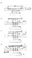
図6に、本実施形態に係る基板搬入方法の一例を説明するための概略図を示す。図6は、搬入搬出領域P2m(図2参照)を介してウエハWを基板処理装置100に搬入する方法を説明するための概略図である。[Board loading method]
FIG. 6 is a schematic diagram for explaining an example of the substrate carry-in method according to the present embodiment. FIG. 6 is a schematic diagram for explaining a method of loading the wafer W into the
ウエハWの搬入搬出は、ウエハ保持機構25を用いて実施される。そのため、ウエハ保持機構25の構成について、簡単に説明し、その後、ウエハ保持機構25を用いた基板処理方法(ウエハWの搬入・搬出方法)について、説明する。 Loading and unloading of the wafer W is performed using the
ウエハ保持機構25は、例えば3本の昇降ピン25aと、各々の昇降ピン25aを収容可能であると共に昇降可能である昇降機構25bを有する。 The
また、凹部24の底面24bには、昇降ピン25aが貫通する貫通孔26が形成されている。ウエハWの凹部24への搬入搬出は、貫通孔26を通過する昇降ピン25aを介して実施される。そのため、貫通孔26の孔径は、昇降ピン25aの径よりも大きく設計される。 A through
昇降機構25bは、昇降ピン25aを垂直方向に移動可能(昇降可能)に構成されると共に、昇降ピン25aを回転テーブル2の径方向内向きへと移動可能に構成される。昇降ピン25aの径方向内向きへの移動は、昇降ピン25aの径に対する貫通孔26の径のクリアランス分の範囲内となる。 The elevating
一般的に、貫通孔26の孔径と、昇降ピン25aのピン径との差分が、昇降ピン25aの径方向に関する最大移動量となる。限定されないが、昇降ピン25aのピン径は、例えばφ3.5mmであっても良く、貫通孔26の孔径は、例えばφ9.5mmであっても良い。また、前述のように、凹部24は、ウエハWの直径よりも僅かに、具体的には1mm乃至4mm程度大きい内径を有する。そのため、昇降ピン25aの径方向内向きの移動量は、凹部24とウエハWとの間の径方向のクリアランスよりも大きくなる。 In general, the difference between the hole diameter of the through
ウエハWの搬入においては、先ず、所定の凹部24が搬入搬出領域P2m(図3参照)に臨む位置に来るように、回転テーブル2を間欠的に回転させる。そして、図6(a)に示すように、昇降ピン25aの端部を凹部24よりも高く保持した状態で、搬送アーム10を用いてウエハWを昇降ピン25aの上方へと移動させる。搬送アーム10に搬送されるウエハWの位置は、昇降ピン25aの端部よりも高い位置となる。なお、本実施形態においては、ウエハWの中心が、概ね凹部24の中心に位置するように、搬送アーム10を用いてウエハWが移動される。 In loading the wafer W, first, the
次に、図6(b)に示すように、更に昇降ピン25aを上方へと移動させ、昇降ピン25aをウエハWに当接させる。そして、更に昇降ピン25aを上方へと移動させる。これにより、ウエハWは、搬送アーム10から上方に所定の距離だけ離間した位置に配置される。 Next, as shown in FIG. 6B, the lift pins 25 a are further moved upward to bring the lift pins 25 a into contact with the wafer W. Then, the elevating
そして、図6(c)に示すように、搬送アーム10を搬送口15から基板処理装置100の外側へと移動させる。 Then, as shown in FIG. 6C, the
最後に、図6(d)に示すように、昇降ピン25aを鉛直下向きに降下させることで、ウエハWを凹部24上に載置する。なお、図6(d)においては、破線により、図6(c)におけるウエハWの位置を示している。 Finally, as shown in FIG. 6D, the wafer W is placed on the
なお、図6(a)に示すように、ウエハWが載置される凹部24の直径D2は、ウエハWの直径D1よりも僅かに、具体的には、1mm乃至4mm程度大きい内径を有する。また、凹部24の深さd2は、ウエハWの厚さd1にほぼ等しいか、又はウエハWの厚さd1よりも大きく構成されている。しかしながら、図6においては、説明の便宜上、凹部24の直径D2が、ウエハWの直径D1に対して、比較的大きい例を概略的に示している。また、凹部24の側壁24aは、凹部24の底面24bに対して、垂直に形成されている例について説明したが、本発明はこの点において限定されず、凹部24は、凹部24の径が底面24bから離れるにつれて大きくなるテーパ形状を有していても良い。 As shown in FIG. 6A, the diameter D2 of the
ウエハWの凹部24への搬入に関して、より好ましい実施形態について、図7を参照して説明する。図7に、本実施形態に係る基板搬入方法の他の例を説明するための概略図を示す。図7(a)乃至図7(c)に対応する工程は、図6(a)乃至図6(c)で説明した工程と同様であるため、同様の説明は省略する。即ち、図7(c)において、ウエハWは昇降ピン25aによって当接しており、搬送アーム10は、搬送口15から基板処理装置100の外側へと移動されている。 A more preferred embodiment regarding loading of the wafer W into the
図7(d)において、昇降ピン25aは、鉛直下向きに移動すると共に、回転テーブル2の回転に関する、径方向外側に移動する。これにより、図7(d)で凹部24に載置されるウエハWは、図6(d)で示されるウエハWの載置位置に対して、径方向外側に移動する。なお、図7(d)においては、破線により、図7(c)におけるウエハWの位置を示している。 In FIG. 7D, the elevating
図7(d)における径方向外側への移動は、ウエハWが凹部24の側壁24aに触れない程度とすることが好ましい。ウエハWが側壁24aに触れた場合、接触箇所からパーティクルが発生することがある。また、ウエハWと側壁24aと擦れることにより、ウエハWの外表面が傷つくことがある。 The movement outward in the radial direction in FIG. 7 (d) is preferably set such that the wafer W does not touch the
図6及び図7を用いて説明したウエハWの凹部24への載置後、ウエハWには、各種処理(例えば成膜処理)が実施される。その際には、回転テーブル2が回転するため、ウエハWは、遠心力によって径方向外側に移動する。図7に示す実施形態では、ウエハWの載置位置が、図6に示す実施形態の場合と比して、回転テーブル2の回転に関する、径方向外側に移動している。これにより、その後の基板処理時(例えば成膜処理時)における回転テーブル2の回転によって、ウエハWに遠心力が印加され、更に径方向外側へ移動した場合であっても、ウエハWと側壁24aの衝突による衝撃を抑制することができる。即ち、図6に示す実施形態と比して、パーティクルの発生や、衝突による外傷の発生を抑制することができる。 After placing the wafer W in the
[基板の搬出方法]
次に、凹部24に載置されたウエハWに対して例えば成膜処理を施した後の、ウエハWの搬出方法について、図を参照して説明する。[Substrate unloading method]
Next, a method for unloading the wafer W after performing, for example, a film forming process on the wafer W placed in the
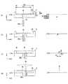
図8に、本実施形態に係る基板搬出方法の一例を説明するための概略図を示す。また、図9に、図8(a)から図8(b)までの昇降ピン25a及びウエハWの移動を説明するための概略図を示す。なお、図9においては、説明の便宜上、図8の図を更に概略的に示している。具体的には、昇降ピン25aは1つだけ記載し、凹部24の径D2及び深さd2が、各々、ウエハWの径D1及び厚さd1に対して、比較的大きい例を概略的に示している。また、各図9における左図は、各々、図9における右図に対応しており、左図の昇降ピン25aが、実線の位置から破線の位置まで直線的に移動したときの、昇降ピン25aの端部の位置が、各々、右図における矢印の始点及び終点に対応している。 FIG. 8 is a schematic diagram for explaining an example of the substrate carry-out method according to the present embodiment. FIG. 9 is a schematic diagram for explaining the movement of the lift pins 25a and the wafer W from FIG. 8 (a) to FIG. 8 (b). In FIG. 9, the diagram of FIG. 8 is more schematically shown for convenience of explanation. Specifically, only one
ウエハWの搬出においては、先ず、所定の凹部24が搬入搬出領域P2m(図3参照)に臨む位置に来るように、回転テーブル2を間欠的に回転させる。 In unloading the wafer W, first, the
この際、成膜処理後のウエハWの中心は、図8(a)に示すように、凹部24の中心に対して、径方向外側に位置している。これは、ウエハWが、回転テーブル2の回転により遠心力の影響を受けるからである。 At this time, the center of the wafer W after the film forming process is located radially outside the center of the
この状態で、図9(a)に示すように、昇降ピン25aを昇降機構25bにより、ウエハWの底面の近傍まで、若しくはウエハWの底面に当接するまで、上昇させる。図9(a)に示す例では、昇降ピン25aが、ウエハWの底面の近傍まで上昇された(即ち、ウエハWの底面から所定の距離離間している)例を示す。なお、昇降ピン25aは、後述する図9(b)において、回転テーブル2の回転に関して径方向内向きに移動するため、この段階においては、貫通孔26の中心に対して径方向外側に移動された状態で、上昇させることが好ましい。 In this state, as shown in FIG. 9A, the elevating
次に、図9(b)に示すように、昇降ピン25aを上昇させる(Z軸方向)と共に、径方向内向き(X軸方向)へと移動させて、昇降ピン25aの端部をウエハWの底面に当接させる。 Next, as shown in FIG. 9B, the lifting pins 25a are raised (Z-axis direction) and moved radially inward (X-axis direction), and the ends of the lifting pins 25a are moved to the wafer W. It is made to contact with the bottom surface of.
そして、図9(c)に示すように、更に昇降ピン25aを上昇させると共に、径方向内向きへと移動させて、ウエハWを凹部24から所定の距離だけ離間させる。なお、図9(b)及び図9(c)における、昇降ピン25aの移動ベクトルの向きは、限定されないが、同じであっても良い。また、図9(b)の終点(即ち、図9(c))における、昇降ピン25aの位置は、凹部24の中心部であっても良い。 Then, as shown in FIG. 9 (c), the raising / lowering pins 25 a are further raised and moved inward in the radial direction to separate the wafer W from the
図9(a)での昇降ピン25aのX軸方向位置と、図9(c)の終点(図9(d)の始点)での昇降ピン25aの径方向位置の差(の絶対値)が、昇降ピン25aの径方向の移動距離となる。これは、昇降ピン25aのピン径と、貫通孔26の孔径との差(の絶対値)の範囲内となるように、当業者が各種パラメータを設定する。 The difference (absolute value) between the position in the X-axis direction of the
最後に、図9(d)に示すように、昇降ピン25aを更に上昇させ、搬送アーム10にウエハWを載置可能となる十分な距離だけ、ウエハWを凹部24から離間させる。結果として、図9(d)に示す状態は、図8(b)に示す状態と同じ状態となる。なお、図9(d)において、昇降ピン25aは鉛直上向きに移動する例を示したが、図9(c)で説明したように、鉛直上向きに移動すると共に、径方向内向きへとする構成であっても良い。 Finally, as shown in FIG. 9D, the lift pins 25 a are further raised, and the wafer W is separated from the
ウエハWを凹部24から十分に離間させた後は、図8(c)に示すように、搬送アーム10をウエハWの底面と凹部24との間に移動させる。そして、図8(d)に示すように、ウエハWを搬送アーム10へと載置し、搬送アーム10を介して、ウエハWは基板処理装置100の外側へと搬出される。 After the wafer W is sufficiently separated from the
本実施形態に係る基板搬出方法は、回転テーブル式の各種基板処理によって、径方向外側に移動したウエハWを、鉛直上向きに移動させると共に、径方向内向きへと移動させる。これにより、ウエハWが、凹部24の側壁24aと接触しないため、搬出時のパーティクル発生量を抑制することができる。また、ウエハWが凹部24の側壁24aと接触しないため、搬出時におけるウエハWの破損を抑制することができる。 In the substrate carry-out method according to the present embodiment, the wafer W moved radially outward is moved vertically upward and moved radially inward by various rotary table type substrate processes. Thereby, since the wafer W does not contact the
なお、図9(c)を用いて説明した、昇降ピン25aがウエハWの底面に接触してからの、昇降ピン25aの径方向内向きへの移動量X1は、凹部24の直径D2及びウエハWの直径D1を使用して、下記式(1)の関係にあることが好ましい。 It should be noted that the movement amount X1 of the lift pins 25a inward in the radial direction after the lift pins 25a contact the bottom surface of the wafer W described with reference to FIG. 9C is the diameter D2 of the
X1<D2−D1 ・・・式(1)
式(1)で示す関係式は、ウエハWの搬出において、ウエハWと、凹部24の側壁24aであって、径方向内側に位置する側壁との接触を防ぐものである。ウエハWの径方向内向きへの移動距離を、所定の値より小さくすることにより、物理的にウエハWは、凹部24の側壁24aと接触しない。なお、式(1)におけるD2−D1は、図9(c)における、実線でのウエハWの右端と、凹部24の側壁との間の距離に対応する。X1 <D2-D1 Formula (1)
The relational expression shown in Expression (1) is to prevent contact between the wafer W and the
若しくは、昇降ピン25aがウエハWの底面に接触してからの、昇降ピン25aの径方向内向きへの移動量X1及び昇降ピン25aの鉛直上向きへの移動量Z1は、凹部24の直径D2、ウエハWの直径D1及び凹部24の深さd2を使用して、下記式(2)の関係にあっても良い。 Alternatively, the amount of movement X1 of the lifting pins 25a inward in the radial direction and the amount of movement Z1 of the lifting pins 25a vertically upward after the lifting pins 25a contact the bottom surface of the wafer W are the diameter D2 of the
Z1/X1>d2/(D2−D1) ・・・式(2)
式(2)の関係は、昇降ピン25aの傾きを所定の値よりも大きい値に規定することにより、ウエハWと、凹部24の側壁24aであって、径方向内側に位置する側壁との接触を防ぐものである。なお、式(2)におけるZ1/X1は、図9(c)における昇降ピン25aの傾きに対応し、式(2)におけるd2/(D2−D1)は、図9(c)における昇降ピン25aの右端と、凹部24の側壁の上端部とを結ぶ直線の傾きに対応する。Z1 / X1> d2 / (D2-D1) (2)
The relationship of Expression (2) is that the inclination of the elevating
なお、式(1)及び式(2)において、ウエハWの直径D1の寸法は、例えば成膜処理後などの各種基板処理後のウエハWに関するものである。成膜処理や熱処理などによりウエハWの寸法が変更される場合には、予めその変更分を考慮したウエハWの直径D1を採用する。 In the expressions (1) and (2), the dimension of the diameter D1 of the wafer W relates to the wafer W after various substrate processing such as after film formation processing. When the dimension of the wafer W is changed by a film forming process or a heat treatment, the diameter D1 of the wafer W is adopted in consideration of the change.
このように、本実施形態に係る基板処理方法(基板搬送方法)は、基板の搬出時に、昇降ピン25aを鉛直上向きに移動させると共に、回転テーブル2の回転に関する径方向内向きに移動させることにより、ウエハWが凹部24の側壁24aと擦れることを防ぐ。結果として、ウエハWからのパーティクルの発生を抑制することができる。 As described above, the substrate processing method (substrate transport method) according to the present embodiment moves the lifting pins 25a vertically upward and moves them radially inward with respect to the rotation of the
本実施形態に係る基板処理方法における、ウエハWを鉛直上向きに移動させると共に、径方向内向きに移動させることにより、パーティクルの発生を抑制する効果について、具体的な実施形態を参照して説明する。 The effect of suppressing the generation of particles by moving the wafer W vertically upward and moving radially inward in the substrate processing method according to the present embodiment will be described with reference to a specific embodiment. .
(第1の実施形態)
図1を用いて説明した基板処理装置100に、図7を用いて基板搬入方法により、回転テーブル2上の2つの凹部24上に、シリコンウエハWを載置した。なお、ウエハWは、直径D1がφ300mmのものを使用し、凹部24は、直径D2がφ302mmであり、深さd2が1.8mmのものを使用した。(First embodiment)
The silicon wafer W was placed on the two
載置されたウエハWに対して、下記の処理条件で、成膜処理を実施した。 A film forming process was performed on the placed wafer W under the following processing conditions.
処理条件としては、
温度:600℃:
圧力:6.7Torr:
第1の反応ガス/流量:トリスジメチルアミノシラン(3DMAS)/300sccm:
第2の反応ガス/流量:N2/420sccm:
回転速度:120rpm:
とした。As processing conditions,
Temperature: 600 ° C:
Pressure: 6.7 Torr:
First reaction gas / flow rate: Trisdimethylaminosilane (3DMAS) / 300 sccm:
The second reaction gas /flow:
Rotational speed: 120 rpm:
It was.
成膜処理後のウエハWの直径D1'は、おおよそφ301mmであった。 The diameter D1 ′ of the wafer W after the film forming process was approximately φ301 mm.
そして、図8で説明した昇降ピン25aの軌道により、1枚のウエハWを凹部24から搬出した。なお、ウエハWに接した後における、昇降ピン25aの径方向内向きの移動量X1は、0.2mmとした。この移動量は、式(1)のX1(0.2mm)<D2(302mm)−D1(301mm)の関係を満たしている。 Then, one wafer W was unloaded from the
また、同時に、比較例として、残りの1枚のウエハWを、昇降ピン25aの軌道を径方向内向きに移動させず、鉛直上向きにして、搬出した。 At the same time, as a comparative example, the remaining one wafer W was unloaded with the trajectory of the elevating
ウエハWの搬出後、各々の凹部24について、パーティクルの発生量を計測した。このステップを1ステップとし、合計5回(実施例1〜5及び比較例1〜5)のステップで、パーティクルの発生量を計測した。 After the wafer W was unloaded, the amount of generated particles was measured for each
図10に、本実施形態に係る基板処理方法後のパーティクル数の一例を示す。 FIG. 10 shows an example of the number of particles after the substrate processing method according to this embodiment.
図10に示されるように、本実施形態に係る基板処理方法は、基板の搬出時において、ウエハWが凹部24の側壁部と擦れないため、パーティクルの発生が抑制されることがわかった。 As shown in FIG. 10, in the substrate processing method according to the present embodiment, it was found that the generation of particles is suppressed because the wafer W does not rub against the side wall of the
1 チャンバ
2 回転テーブル
11 天板
12 容器本体
13 シール部材
24 凹部
25 ウエハ保持機構
26 貫通孔
31 ガスノズル
32 反応ガスノズル
41 分離ガスノズル
42 分離ガスノズル
44 天井面
81 加熱ランプ
86 透過部材
100 基板処理装置
101 制御部
102 記憶部
103 媒体
610 排気口
640 真空ポンプ
W ウエハDESCRIPTION OF SYMBOLS 1
Claims (12)
Translated fromJapanese前記容器内に回転可能に設けられ、表面に前記基板を載置する凹部と前記凹部に連通する貫通孔とが形成されている、回転テーブルと、
前記凹部に載置された前記基板を移載する際に用いる昇降ピンを有する昇降機構と、
前記昇降機構の作動を制御する制御部と、
を有し、
前記制御部は、前記昇降ピンを径方向に移動させることなく、前記基板の下方から前記基板の底面の近傍まで、若しくは前記基板の底面に当接するまで鉛直上向きに移動させた後、前記昇降ピンが前記貫通孔を介して前記基板に当接した状態で、前記昇降ピンを鉛直上向きに移動させながら、前記昇降ピンを前記回転テーブルの回転に関する径方向内向きに移動させることで、前記基板を前記凹部から搬出するように前記昇降機構を制御する、
基板処理装置。A substrate processing apparatus for forming a film containing a reaction product on a substrate by executing a supply cycle in which at least two kinds of reaction gases that react with each other in a container are sequentially supplied to the surface of the substrate a plurality of times. And
A turntable that is rotatably provided in the container, and has a recess on which the substrate is placed and a through hole communicating with the recess;
An elevating mechanism having elevating pins used when transferring the substrate placed in the recess;
A control unit for controlling the operation of the lifting mechanism;
Have
The control unitmoves the lifting pin vertically upward from below the substrate to near the bottom surface of the substrate or until it contacts the bottom surface of the substrate without moving the lifting pin in the radial direction. In the state where the substrate is in contact with the substrate via the through hole, the substrate is moved by moving the lift pin vertically upward while moving the lift pin vertically upward. Controlling the elevating mechanism to carry out from the recess,
Substrate processing equipment.
X1<D2−D1の関係にある、
請求項1に記載の基板処理装置。The amount X1 of the lifting pin that moves inward in the radial direction after the lifting pins abut on the substrate is determined by the diameter D1 of the substrate placed in the recess and the diameter D2 of the recess. make use of,
X1 <D2-D1
The substrate processing apparatus according to claim 1.
前記昇降ピンの前記径方向内向きへの移動量X1と、前記昇降ピンの鉛直上向きへの移動量Z1と、前記凹部に載置された前記基板の直径D1と、前記凹部の直径D2と、前記凹部の深さd2とは、Z1/X1>d2/(D2−D1)の関係にある、
請求項1に記載の基板処理装置。While the elevating pin is in contact with the substrate and moving vertically upward and radially inward,
A moving amount X1 of the elevating pin inward in the radial direction, a moving amount Z1 of the elevating pin in a vertically upward direction, a diameter D1 of the substrate placed in the recess, and a diameter D2 of the recess, The depth d2 of the recess is in a relationship of Z1 / X1> d2 / (D2-D1).
The substrate processing apparatus according to claim 1.
前記第1の供給領域から前記回転テーブルの回転方向に沿って離間する第2の供給領域に配置され、前記凹部上の前記基板へ第2の反応ガスを供給する第2の反応ガス供給部と、
を更に有する、請求項1乃至3のいずれか一項に記載の基板処理装置。A first reaction gas supply unit disposed in a first supply region in the container and supplying a first reaction gas to the substrate on the recess;
A second reaction gas supply unit that is disposed in a second supply region that is spaced apart from the first supply region along the rotation direction of the turntable, and that supplies a second reaction gas to the substrate on the recess; ,
The substrate processing apparatus according to claim 1, further comprising:
前記分離ガス供給部を形成する空間の高さは、前記第1の反応ガス供給部及び前記第2の反応ガス供給部の各々を形成する空間の高さよりも低い、
請求項5に記載の基板処理装置。The separation gas supply unit has a ceiling surface that forms a separation space having a predetermined height with a surface of the turntable on which the substrate is placed.
The height of the space forming the separation gas supply unit is lower than the height of the space forming each of the first reaction gas supply unit and the second reaction gas supply unit.
The substrate processing apparatus according to claim 5.
各々の前記凹部に対して、3本の前記昇降ピンが設けられる、
請求項1乃至6のいずれか一項に記載の基板処理装置。A plurality of the recesses are provided in the rotary table,
Three lifting pins are provided for each of the recesses,
The substrate processing apparatus according to claim 1.
前記昇降ピンを径方向に移動させることなく、前記基板の下方から前記基板の底面の近傍まで、若しくは前記基板の底面に当接するまで鉛直上向きに移動させる工程と、
前記昇降ピンが前記貫通孔を介して前記基板に当接した状態で、前記昇降ピンを鉛直上向きに移動させながら、前記昇降ピンを前記回転テーブルの回転に関する径方向内向きに移動させることで、前記基板を前記凹部から搬出する工程と、
を有する、
基板処理方法。In a state where the substrate is placed on the concave portion of the rotary table, the concave portion for rotatably placing the substrate on the surface and a through hole communicating with the concave portion are formed on the surface. A substrate processing method for carrying out the processing on the substrate while rotating a turntable, and then unloading the substrate placed in the recess using an elevating mechanism having elevating pins,
Without vertically moving the lifting pins, from the bottom of the substrate to the vicinity of the bottom surface of the substrate, or to move vertically up to contact with the bottom surface of the substrate;
In the state where the lifting pins are in contact with the substrate through the through holes, the lifting pins are moved inward in the radial direction with respect to the rotation of the rotary table while moving the lifting pins vertically upward, Unloading the substrate from the recess;
Having
Substrate processing method.
請求項8に記載の基板処理方法。The movement amount X1 of the lifting pins inward in the radial direction after the lifting pins contact the substrate, the diameter D1 of the substrate placed in the recess, and the diameter D2 of the recess , X1 <D2-D1
The substrate processing method according to claim 8.
前記昇降ピンの前記径方向内向きへの移動量X1と、前記昇降ピンの鉛直上向きへの移動量Z1と、前記凹部に載置された前記基板の直径D1と、前記凹部の直径D2と、前記凹部の深さd2とは、Z1/X1>d2/(D2−D1)の関係にある、
請求項8に記載の基板処理方法。While the elevating pin is in contact with the substrate and moving vertically upward and radially inward,
A moving amount X1 of the elevating pin inward in the radial direction, a moving amount Z1 of the elevating pin in a vertically upward direction, a diameter D1 of the substrate placed in the recess, and a diameter D2 of the recess, The depth d2 of the recess is in a relationship of Z1 / X1> d2 / (D2-D1).
The substrate processing method according to claim 8.
前記基板の下方から、前記昇降ピンと前記基板との距離が所定の距離となるまで、前記昇降ピンを鉛直上向きに移動させる工程と、
前記昇降ピンを鉛直上向きに移動させながら、前記昇降ピンを前記回転テーブルの回転に関する径方向内向きに移動させて、前記昇降ピンを前記基板に当接させる工程と、
を有する、請求項8乃至10のいずれか一項に記載の基板処理方法。The contact of the lifting pins with the substrate is as follows:
Moving the lifting pins vertically upward from below the substrate until the distance between the lifting pins and the substrate is a predetermined distance;
Moving the elevating pins vertically upward while moving the elevating pins radially inward with respect to the rotation of the rotary table, and bringing the elevating pins into contact with the substrate;
The substrate processing method according to claim 8, comprising:
前記基板を保持するための基板保持アームを、前記昇降ピンと前記凹部との間に移動させる工程と、
前記昇降ピンを下降させて、前記基板を前記基板保持アームへと載置する工程と、
を有する、請求項8乃至11のいずれか一項に記載の基板処理方法。After the unloading step,
Moving a substrate holding arm for holding the substrate between the elevating pin and the recess;
Lowering the lift pins to place the substrate on the substrate holding arm;
The substrate processing method according to claim 8, comprising:
Priority Applications (5)
| Application Number | Priority Date | Filing Date | Title |
|---|---|---|---|
| JP2013193412AJP6114668B2 (en) | 2013-09-18 | 2013-09-18 | Substrate processing apparatus and substrate processing method |
| US14/482,047US10837110B2 (en) | 2013-09-18 | 2014-09-10 | Substrate processing apparatus and method for processing a substrate |
| TW103131838ATWI579954B (en) | 2013-09-18 | 2014-09-16 | Substrate processing apparatus and method for processing a substrate |
| KR1020140123453AKR101786167B1 (en) | 2013-09-18 | 2014-09-17 | Substrate processing apparatus and substrate processing method |
| CN201410479020.1ACN104451602A (en) | 2013-09-18 | 2014-09-18 | Substrate processing apparatus and method for processing a substrate |
Applications Claiming Priority (1)
| Application Number | Priority Date | Filing Date | Title |
|---|---|---|---|
| JP2013193412AJP6114668B2 (en) | 2013-09-18 | 2013-09-18 | Substrate processing apparatus and substrate processing method |
Publications (2)
| Publication Number | Publication Date |
|---|---|
| JP2015060936A JP2015060936A (en) | 2015-03-30 |
| JP6114668B2true JP6114668B2 (en) | 2017-04-12 |
Family
ID=52668112
Family Applications (1)
| Application Number | Title | Priority Date | Filing Date |
|---|---|---|---|
| JP2013193412AActiveJP6114668B2 (en) | 2013-09-18 | 2013-09-18 | Substrate processing apparatus and substrate processing method |
Country Status (5)
| Country | Link |
|---|---|
| US (1) | US10837110B2 (en) |
| JP (1) | JP6114668B2 (en) |
| KR (1) | KR101786167B1 (en) |
| CN (1) | CN104451602A (en) |
| TW (1) | TWI579954B (en) |
Families Citing this family (17)
| Publication number | Priority date | Publication date | Assignee | Title |
|---|---|---|---|---|
| US9416448B2 (en)* | 2008-08-29 | 2016-08-16 | Tokyo Electron Limited | Film deposition apparatus, substrate processing apparatus, film deposition method, and computer-readable storage medium for film deposition method |
| JP5107185B2 (en) | 2008-09-04 | 2012-12-26 | 東京エレクトロン株式会社 | Film forming apparatus, substrate processing apparatus, film forming method, and recording medium recording program for executing this film forming method |
| US9297072B2 (en) | 2008-12-01 | 2016-03-29 | Tokyo Electron Limited | Film deposition apparatus |
| JP6114668B2 (en)* | 2013-09-18 | 2017-04-12 | 東京エレクトロン株式会社 | Substrate processing apparatus and substrate processing method |
| JP6262115B2 (en) | 2014-02-10 | 2018-01-17 | 東京エレクトロン株式会社 | Substrate processing method and substrate processing apparatus |
| CN107438897A (en)* | 2015-04-09 | 2017-12-05 | 应用材料公司 | Carrier system for pending substrate |
| JP6669481B2 (en)* | 2015-12-04 | 2020-03-18 | 株式会社ブイ・テクノロジー | Inspection device |
| JP6548586B2 (en) | 2016-02-03 | 2019-07-24 | 東京エレクトロン株式会社 | Deposition method |
| JP6733516B2 (en) | 2016-11-21 | 2020-08-05 | 東京エレクトロン株式会社 | Method of manufacturing semiconductor device |
| JP2020177967A (en)* | 2019-04-16 | 2020-10-29 | 東京エレクトロン株式会社 | Substrate processing apparatus |
| JP7636892B2 (en) | 2020-01-06 | 2025-02-27 | エーエスエム・アイピー・ホールディング・ベー・フェー | Channeled Lift Pins |
| FI130143B (en)* | 2020-10-12 | 2023-03-10 | Beneq Oy | An atomic layer deposition apparatus and a method |
| JP7634390B2 (en)* | 2021-03-12 | 2025-02-21 | 東京エレクトロン株式会社 | SUBSTRATE PROCESSING APPARATUS AND METHOD FOR CONTROLLING SUBSTRATE PROCESSING APPARATUS |
| JP2023032647A (en)* | 2021-08-27 | 2023-03-09 | 株式会社Kokusai Electric | Substrate processing device, manufacturing method for semiconductor device, and recording medium |
| JP2023091605A (en) | 2021-12-20 | 2023-06-30 | 東京エレクトロン株式会社 | Substrate processing apparatus and substrate unloading method |
| CN116705674A (en)* | 2022-02-25 | 2023-09-05 | 安益隆展业股份有限公司 | Component processing equipment and component carrier device thereof |
| JP2024124987A (en) | 2023-03-03 | 2024-09-13 | 東京エレクトロン株式会社 | Substrate processing apparatus and control position setting method |
Family Cites Families (16)
| Publication number | Priority date | Publication date | Assignee | Title |
|---|---|---|---|---|
| JPH0897274A (en)* | 1994-09-22 | 1996-04-12 | Dainippon Screen Mfg Co Ltd | Substrate transfer device |
| JPH09147786A (en)* | 1995-11-21 | 1997-06-06 | Advanced Display:Kk | Method for holding substrate, and substrate holding mechanism used therefor |
| JP4330703B2 (en)* | 1999-06-18 | 2009-09-16 | 東京エレクトロン株式会社 | Transport module and cluster system |
| JP4661990B2 (en) | 2008-06-27 | 2011-03-30 | 東京エレクトロン株式会社 | Film forming apparatus, film forming method, substrate processing apparatus, and storage medium |
| US20090324826A1 (en)* | 2008-06-27 | 2009-12-31 | Hitoshi Kato | Film Deposition Apparatus, Film Deposition Method, and Computer Readable Storage Medium |
| CN101665923A (en)* | 2008-09-04 | 2010-03-10 | 东京毅力科创株式会社 | Film deposition apparatus, substrate processing apparatus and film deposition method |
| JP5280964B2 (en) | 2008-09-04 | 2013-09-04 | 東京エレクトロン株式会社 | Film forming apparatus, substrate processing apparatus, film forming method, and storage medium |
| US7964038B2 (en)* | 2008-10-02 | 2011-06-21 | Applied Materials, Inc. | Apparatus for improved azimuthal thermal uniformity of a substrate |
| US8314371B2 (en)* | 2008-11-06 | 2012-11-20 | Applied Materials, Inc. | Rapid thermal processing chamber with micro-positioning system |
| JP5310512B2 (en) | 2009-12-02 | 2013-10-09 | 東京エレクトロン株式会社 | Substrate processing equipment |
| JP2012195427A (en) | 2011-03-16 | 2012-10-11 | Ulvac Japan Ltd | Substrate processing apparatus and substrate processing method |
| WO2013162774A1 (en)* | 2012-04-27 | 2013-10-31 | Applied Materials, Inc. | Method and apparatus for independent wafer handling |
| JP6114668B2 (en)* | 2013-09-18 | 2017-04-12 | 東京エレクトロン株式会社 | Substrate processing apparatus and substrate processing method |
| JP6512063B2 (en)* | 2015-10-28 | 2019-05-15 | 東京エレクトロン株式会社 | Film deposition system |
| US10428425B2 (en)* | 2016-01-26 | 2019-10-01 | Tokyo Electron Limited | Film deposition apparatus, method of depositing film, and non-transitory computer-readable recording medium |
| JP6628634B2 (en)* | 2016-02-22 | 2020-01-15 | 東京エレクトロン株式会社 | Film forming apparatus, film forming method, program, and computer-readable storage medium |
- 2013
- 2013-09-18JPJP2013193412Apatent/JP6114668B2/enactiveActive
- 2014
- 2014-09-10USUS14/482,047patent/US10837110B2/enactiveActive
- 2014-09-16TWTW103131838Apatent/TWI579954B/enactive
- 2014-09-17KRKR1020140123453Apatent/KR101786167B1/enactiveActive
- 2014-09-18CNCN201410479020.1Apatent/CN104451602A/enactivePending
Also Published As
| Publication number | Publication date |
|---|---|
| KR20150032494A (en) | 2015-03-26 |
| CN104451602A (en) | 2015-03-25 |
| US20150078864A1 (en) | 2015-03-19 |
| TWI579954B (en) | 2017-04-21 |
| JP2015060936A (en) | 2015-03-30 |
| KR101786167B1 (en) | 2017-10-17 |
| US10837110B2 (en) | 2020-11-17 |
| TW201521143A (en) | 2015-06-01 |
Similar Documents
| Publication | Publication Date | Title |
|---|---|---|
| JP6114668B2 (en) | Substrate processing apparatus and substrate processing method | |
| JP6330623B2 (en) | Film forming apparatus, film forming method, and storage medium | |
| JP5107185B2 (en) | Film forming apparatus, substrate processing apparatus, film forming method, and recording medium recording program for executing this film forming method | |
| JP5068780B2 (en) | Film forming apparatus, film forming method, program, and computer-readable storage medium | |
| JP6478847B2 (en) | Substrate processing equipment | |
| TWI613312B (en) | Method for processing a substrate and substrate processing apparatus | |
| JP2010126797A (en) | Film deposition system, semiconductor fabrication apparatus, susceptor for use in the same, program and computer readable storage medium | |
| JP2016143836A (en) | Substrate processing equipment | |
| JP2010059498A (en) | Film deposition apparatus, substrate treating apparatus, film deposition method and recording medium which records program for executing the film deposition method therein | |
| US11214864B2 (en) | Method for reducing metal contamination and film deposition apparatus | |
| JP5195176B2 (en) | Deposition equipment | |
| JP6512063B2 (en) | Film deposition system | |
| JP2018093121A (en) | Cleaning method | |
| JP6735549B2 (en) | Substrate processing apparatus, substrate processing method and ring-shaped member | |
| KR20170005761A (en) | Film-forming processing apparatus, film-forming method, and storage medium | |
| JP6456712B2 (en) | Substrate holding mechanism and substrate processing apparatus using the same | |
| JP6971887B2 (en) | Film formation method and film formation equipment | |
| US10458016B2 (en) | Method for forming a protective film | |
| JP6494495B2 (en) | Substrate processing method and substrate processing apparatus | |
| JP2015070095A (en) | Substrate processing apparatus and substrate processing method | |
| JP6096588B2 (en) | Substrate processing apparatus and substrate processing method | |
| US20220389581A1 (en) | Substrate processing apparatus and substrate processing method | |
| JP6481363B2 (en) | Film forming apparatus, film forming method, and storage medium | |
| JP6441050B2 (en) | Deposition method |
Legal Events
| Date | Code | Title | Description |
|---|---|---|---|
| A621 | Written request for application examination | Free format text:JAPANESE INTERMEDIATE CODE: A621 Effective date:20160328 | |
| A977 | Report on retrieval | Free format text:JAPANESE INTERMEDIATE CODE: A971007 Effective date:20161226 | |
| A131 | Notification of reasons for refusal | Free format text:JAPANESE INTERMEDIATE CODE: A131 Effective date:20170104 | |
| A521 | Request for written amendment filed | Free format text:JAPANESE INTERMEDIATE CODE: A523 Effective date:20170223 | |
| TRDD | Decision of grant or rejection written | ||
| A01 | Written decision to grant a patent or to grant a registration (utility model) | Free format text:JAPANESE INTERMEDIATE CODE: A01 Effective date:20170314 | |
| A61 | First payment of annual fees (during grant procedure) | Free format text:JAPANESE INTERMEDIATE CODE: A61 Effective date:20170317 | |
| R150 | Certificate of patent or registration of utility model | Ref document number:6114668 Country of ref document:JP Free format text:JAPANESE INTERMEDIATE CODE: R150 | |
| R250 | Receipt of annual fees | Free format text:JAPANESE INTERMEDIATE CODE: R250 | |
| R250 | Receipt of annual fees | Free format text:JAPANESE INTERMEDIATE CODE: R250 | |
| R250 | Receipt of annual fees | Free format text:JAPANESE INTERMEDIATE CODE: R250 | |
| R250 | Receipt of annual fees | Free format text:JAPANESE INTERMEDIATE CODE: R250 | |
| R250 | Receipt of annual fees | Free format text:JAPANESE INTERMEDIATE CODE: R250 | |
| R250 | Receipt of annual fees | Free format text:JAPANESE INTERMEDIATE CODE: R250 |