JP6108892B2 - Electronic device and power supply control method - Google Patents
Electronic device and power supply control methodDownload PDFInfo
- Publication number
- JP6108892B2 JP6108892B2JP2013055418AJP2013055418AJP6108892B2JP 6108892 B2JP6108892 B2JP 6108892B2JP 2013055418 AJP2013055418 AJP 2013055418AJP 2013055418 AJP2013055418 AJP 2013055418AJP 6108892 B2JP6108892 B2JP 6108892B2
- Authority
- JP
- Japan
- Prior art keywords
- sensor
- power supply
- detection target
- power
- detection
- Prior art date
- Legal status (The legal status is an assumption and is not a legal conclusion. Google has not performed a legal analysis and makes no representation as to the accuracy of the status listed.)
- Expired - Fee Related
Links
Images


Classifications
- G—PHYSICS
- G06—COMPUTING OR CALCULATING; COUNTING
- G06F—ELECTRIC DIGITAL DATA PROCESSING
- G06F1/00—Details not covered by groups G06F3/00 - G06F13/00 and G06F21/00
- G06F1/26—Power supply means, e.g. regulation thereof
- G06F1/32—Means for saving power
- G06F1/3203—Power management, i.e. event-based initiation of a power-saving mode
- G06F1/3206—Monitoring of events, devices or parameters that trigger a change in power modality
- G06F1/3231—Monitoring the presence, absence or movement of users
- G—PHYSICS
- G06—COMPUTING OR CALCULATING; COUNTING
- G06F—ELECTRIC DIGITAL DATA PROCESSING
- G06F1/00—Details not covered by groups G06F3/00 - G06F13/00 and G06F21/00
- G06F1/26—Power supply means, e.g. regulation thereof
- G06F1/32—Means for saving power
- G06F1/3203—Power management, i.e. event-based initiation of a power-saving mode
- G06F1/3234—Power saving characterised by the action undertaken
- G06F1/325—Power saving in peripheral device
- G—PHYSICS
- G06—COMPUTING OR CALCULATING; COUNTING
- G06F—ELECTRIC DIGITAL DATA PROCESSING
- G06F1/00—Details not covered by groups G06F3/00 - G06F13/00 and G06F21/00
- G06F1/26—Power supply means, e.g. regulation thereof
- G06F1/32—Means for saving power
- G06F1/3203—Power management, i.e. event-based initiation of a power-saving mode
- G06F1/3234—Power saving characterised by the action undertaken
- G06F1/3287—Power saving characterised by the action undertaken by switching off individual functional units in the computer system
- Y—GENERAL TAGGING OF NEW TECHNOLOGICAL DEVELOPMENTS; GENERAL TAGGING OF CROSS-SECTIONAL TECHNOLOGIES SPANNING OVER SEVERAL SECTIONS OF THE IPC; TECHNICAL SUBJECTS COVERED BY FORMER USPC CROSS-REFERENCE ART COLLECTIONS [XRACs] AND DIGESTS
- Y02—TECHNOLOGIES OR APPLICATIONS FOR MITIGATION OR ADAPTATION AGAINST CLIMATE CHANGE
- Y02D—CLIMATE CHANGE MITIGATION TECHNOLOGIES IN INFORMATION AND COMMUNICATION TECHNOLOGIES [ICT], I.E. INFORMATION AND COMMUNICATION TECHNOLOGIES AIMING AT THE REDUCTION OF THEIR OWN ENERGY USE
- Y02D10/00—Energy efficient computing, e.g. low power processors, power management or thermal management
Landscapes
- Engineering & Computer Science (AREA)
- Theoretical Computer Science (AREA)
- General Engineering & Computer Science (AREA)
- Physics & Mathematics (AREA)
- General Physics & Mathematics (AREA)
- Computer Hardware Design (AREA)
- Computing Systems (AREA)
- Power Sources (AREA)
- Geophysics And Detection Of Objects (AREA)
Description
Translated fromJapanese本発明は、外部の検知対象の移動を検知するための複数のセンサを有する電子機器および電源制御方法に関する。 The present invention relates to an electronic apparatus having a plurality of sensors for detecting movement of an external detection target and a power supply control method.
複数のセンサを併用して、センシング対象の変化を時系列として検知するための検知システムが知られている。例えば、人等の熱源の存在を検知する赤外線センサを地点Aと地点Bに2つ用意し、地点Aと地点Bの各センサが検知した時刻を重ね合わせることで、検知対象の人が地点Aから地点Bに移動したことを検出することができる。そのような構成においてセンサの数や種類を多くするほど、より高精度に検出することができる。 A detection system for detecting a change of a sensing target as a time series using a plurality of sensors is known. For example, two infrared sensors that detect the presence of a heat source such as a person are prepared at point A and point B, and the time detected by each of the sensors at point A and point B is overlapped, so that the person to be detected becomes point A It is possible to detect that the user has moved from point to point B. In such a configuration, detection can be performed with higher accuracy as the number and types of sensors are increased.
特許文献1では、低解像度で広い範囲を検知可能なセンサと、高解像度で狭い範囲を検知可能なセンサとを組み合わせる構成が記載されている。そのような構成において、人の接近を前者のセンサで検知した後、後者のセンサを用いて具体的にはどの方位に人が存在するのかを検知することで、少ないセンサ数で人が存在する方位を精密に検知することができると記載されている。 Patent Document 1 describes a configuration in which a sensor capable of detecting a wide range at a low resolution and a sensor capable of detecting a narrow range at a high resolution are combined. In such a configuration, after detecting the approach of the person with the former sensor, the person with a small number of sensors exists by detecting in which direction the person exists using the latter sensor. It is described that the orientation can be detected accurately.
一般的に、センサには、センサ用の電源供給線と、検知したことをCPU等に通知するための検知信号線とが接続されている。システム内のセンサが多くなるほど、検知信号線も多くなり、通知先であるCPUのI/Oポートを消費してしまう。また、システム全体でセンサが消費する総消費電力も大きくなってしまう。しかしながら、必要なセンサのみ電源を投入させるための電源制御線を構成したとしても、その電源制御線のためにCPUのI/Oポートをさらに消費することになってしまう。 In general, a sensor power supply line and a detection signal line for notifying a CPU or the like of detection are connected to the sensor. As the number of sensors in the system increases, the number of detection signal lines also increases, and the I / O port of the CPU that is the notification destination is consumed. In addition, the total power consumption of the sensor in the entire system also increases. However, even if a power control line for turning on only the necessary sensors is configured, the CPU I / O port is further consumed for the power control line.
しかしながら、必要なセンサのみ電源を投入させるための電源制御の構成では、CPUは常に稼働状態でなければならない。従って、CPUの消費電力が大きい場合には、電源制御により不要なセンサの電源をオフさせて削減することができた電力を相殺してしまうことも考えられる。また、CPUではなく、専用のICやエンコーダ・デコーダを介して電源制御を行うように構成したとしても、検知システムがより複雑になってしまう。 However, in a configuration of power control for turning on only necessary sensors, the CPU must always be in an operating state. Therefore, when the power consumption of the CPU is large, it may be possible to cancel the power that can be reduced by turning off unnecessary sensor power by power control. Even if the power supply is controlled via a dedicated IC or encoder / decoder instead of the CPU, the detection system becomes more complicated.
本発明の目的は、このような従来の問題点を解決することにある。本発明は、上記の点に鑑み、複数のセンサを用いて検知対象を検知する電子機器であって消費電力を低減する電子機器および電源制御方法を提供することを目的とする。 An object of the present invention is to solve such conventional problems. In view of the above-described points, an object of the present invention is to provide an electronic device that detects a detection target using a plurality of sensors and that reduces power consumption and a power control method.
上記課題を解決するため、本発明に係る電子機器は、第1の領域の検知対象を検知する第1のセンサと、第2の領域の検知対象を検知する第2のセンサと、第3の領域の検知対象を検知する第3のセンサと、前記第1のセンサが前記第1の領域の前記検知対象を検知する場合に前記第2のセンサの電源をオンとし、前記第2のセンサが前記第2の領域の前記検知対象を検知する場合に前記第3のセンサの電源をオンとし、前記第1のセンサの電源をオフとする電源制御手段と、を備えることを特徴とする。In order to solve the above problems, an electronic device according to the present invention includesa first sensor that detects a detection target in a first region, a second sensor that detects a detection target in a second region, and a third sensor a third sensor for detecting the detection target region, the first sensorand turns on the power ofthe second sensorwhen detecting the detection targetof the firstregion,the second sensor There power of the third sensor is turned on when detecting the detection target of the second region, characterized in that it comprisesa power supply control meansfor turning off the power of the first sensor.
本発明によれば、複数のセンサを用いて検知対象を検知する電子機器において消費電力を低減することができる。 ADVANTAGE OF THE INVENTION According to this invention, power consumption can be reduced in the electronic device which detects a detection target using a some sensor.
以下、添付図面を参照して本発明の好適な実施形態を詳しく説明する。尚、以下の実施形態は特許請求の範囲に係る本発明を限定するものでなく、また本実施形態で説明されている特徴の組み合わせの全てが本発明の解決手段に必須のものとは限らない。なお、同一の構成要素には同一の参照番号を付して、説明を省略する。 Hereinafter, preferred embodiments of the present invention will be described in detail with reference to the accompanying drawings. The following embodiments do not limit the present invention according to the claims, and all combinations of features described in the embodiments are not necessarily essential to the solution means of the present invention. . The same constituent elements are denoted by the same reference numerals, and the description thereof is omitted.
〔第1の実施形態〕
図1は、複数のセンサにより、装置外部の人等の検知対象の移動を検知可能な検知システム101の構成を示す図である。本実施形態において、検知システム101は、プリンタやスキャナ、又はそれら複数の機能が一体化されたMFP等に代表される画像処理装置に搭載されている。以下、画像処理装置を、検知システム101を有する装置として、単に電子機器ともいう。検知システム101は、コントローラ102、第1のセンサ103、第2のセンサ(中間センサ)104、第3のセンサ(最終センサ)105の3種類のセンサ、電源ユニット106、メインスイッチ107、ACコンセント108を含んでいる。コントローラ102は、CPU121、CPU121が一時記憶として使用するRAM122、CPU121が実行する各種のプログラムを記憶するROM123を含んでいる。CPU121に電源が投入されると、CPU121は、ROM123からプログラムをRAM122にロードして実行し、検知システム101が搭載されている画像処理装置にの各機能を実現する。画像処理装置は、検知システム101により、人の接近を検知したときに省電力モードから通常モードに復帰することができ、また、人が離れたことを検知したときに省電力モードとすることができる。本実施形態で用いられる各センサは、外部の人等の検知対象の存在を検知できるセンサであり、例えば、赤外線センサや焦電センサでも良い。また、各センサはそれぞれ異なる検知領域を有することにより、検知対象の移動、つまり画像処理装置に対して近づくか若しくは離れるかを検出することができる。各センサの検知領域については、図3にて後述する。[First Embodiment]
FIG. 1 is a diagram illustrating a configuration of a
第1のセンサ103には、検知信号線131とセンサ用電源供給線171とが接続されている。中間センサ104には、検知信号線141とセンサ用電源供給線181とが接続されている。最終センサ105には、検知信号線151とセンサ用電源供給線191とが接続されている。ここで、検知信号線131、141、151は、各対応するセンサの検知信号出力端子に接続されている。また、センサ用電源供給線171、181、191は、各対応するセンサの電源端子に接続されている。各センサ用電源供給線171、181、191はそれぞれ、電源の供給を行うためのスイッチを開閉するためのセンサ電源用リレー132、142、152の出力端子に接続されている。 A
検知信号線131は、AND回路193の入力端子に接続されている。また、CPU121からセンサ用電源制御線124が、AND回路193の入力端子に反転接続されている。AND回路193の出力端子は、センサ電源用リレー142のイネーブル端子に接続されている。検知信号線141は、センサ電源用リレー152のイネーブル端子、及び電源ユニット106のメイン電源161のイネーブル端子に接続されている。検知信号線151は、CPU121のリセット端子に接続され、かつ、AND回路192の入力端子に反転接続されている。また、検知システム101の主電源スイッチであるメインスイッチ107の出力信号線がAND回路192の入力端子に接続されており、AND回路192の出力端子は、センサ電源用リレー132のイネーブル端子に接続されている。各センサ103〜105から検知信号線に出力される検知信号の状態(ステータス)、及び、CPU121から出力されるセンサ用電源制御線124の状態は、各デバイス内の不図示のラッチ回路により、各デバイスの電源状態によらずラッチされる。 The
電源ユニット106は、メイン電源161とサブ電源162を含んでいる。メイン電源161は、コントローラ102用の電源を生成する例えばAC/DCコンバータ電源モジュールであり、電源供給線がコントローラ102に接続されている。また、先述のとおり、メイン電源161のイネーブル端子には、中間センサ104からの検知信号線141が接続されている。メイン電源161のイネーブル端子がアクティブ状態になると、メイン電源161は、コントローラ102に電源を供給することができる。 The
サブ電源162は、各センサに供給される電源を生成する例えばAC/DCコンバータ電源モジュールである。サブ電源162の電源供給線は、各センサ電源用リレー132、142、152に接続されている。サブ電源162のイネーブル端子がアクティブ状態になると、サブ電源162は、各センサ電源用リレー132、142、152に電源を供給することができる。メインスイッチ107の出力信号線は、サブ電源162のイネーブル端子にも接続されており、メインスイッチ107をオン状態とすると、サブ電源162のイネーブル端子がアクティブ状態となる。各センサ電源用リレー132、142、152のイネーブル端子がアクティブ状態になると、サブ電源162から供給されている電源をさらに対応する各センサ103〜105に供給することができる。ACコンセント108は、メイン電源161とサブ電源162とにAC電力を供給する。検知システム101が搭載されている画像処理装置の各部に電力が供給されている通常動作モードにおいては、メイン電源161のイネーブル端子はアクティブ状態である。また、画像処理装置内で電源の供給が通常動作モードより制限された省電力モードにおいては、メイン電源161のイネーブル端子は非アクティブ状態であり、サブ電源162のイネーブル端子はアクティブ状態である。 The
図2は、各センサ103〜105の内部の構成を示す図である。各センサ103〜105は、発光部202と受光部203を有する検知ユニット201、検知信号線204、電源供給線205を含んでいる。ここで、検知信号線204は、図1の検知信号線131、141、151に対応する。また、電源供給線205は、図1の電源供給線171、181、191に対応する。発光部202は、赤外線LEDを備え、赤外線を放射する。受光部203は、赤外線を検知する。センサの検知範囲に人等の検知対象が存在する場合には、発光部202から放射された赤外線は検知物に反射し、受光部203がその反射された赤外線を検知する。受光部203は、反射された赤外線を検知すると、検知信号線204をアクティブ状態とする。そのような構成により、各センサ103〜105は、検知信号線204を介して、検知対象を検知した旨をセンサ外部に通知することができる。検知ユニット201に接続される電源供給線205は、発光部202と受光部203に接続されており、電源供給線205から電力が供給されることにより検知ユニット201が動作する。 FIG. 2 is a diagram illustrating an internal configuration of each of the
次に、図1、図3、図4、図5、図6を参照して、検知システム101における各センサの電源制御処理について説明する。 Next, with reference to FIGS. 1, 3, 4, 5, and 6, a power control process for each sensor in the
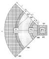
図3は、第1のセンサ103、中間センサ104、最終センサ105の各検知範囲を示す図である。各センサの検知領域は、検知システムが搭載された画像処理装置から遠い順に第1のセンサ103の検知領域、中間センサ104の検知領域、最終センサ105の検知領域となっている。第1のセンサ103の検知領域301と中間センサ104の検知領域302とは一部重複している。また、中間センサ104の検知領域302と最終センサ105の検知領域303とは一部重複している。 FIG. 3 is a diagram illustrating detection ranges of the
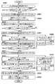
まず、人等の検知対象がA点から検知システム101が搭載された画像処理装置に接近する場合について説明する。図4は、接近時における検知システム101の電源制御処理の手順を示すフローチャートである。 First, a case will be described in which a detection target such as a person approaches from the point A to an image processing apparatus on which the
検知システム101の初期状態においては、検知信号線131、141、151は全て非アクティブ状態である。メインスイッチ107をオンにすると、第1のセンサ103の電源のみがメインスイッチ107によってオンとなる。その結果、第1のセンサ103は、検知領域301の検知対象物の走査を開始する(S401)。その際に、AND回路192は、非アクティブ状態の検知信号151の反転入力と、メインスイッチ107からのアクティブ状態の出力信号線とによって、センサ電源用リレー132のイネーブル端子をアクティブ状態としている。また、検知信号線131及び141が非アクティブ状態であるので、センサ電源用リレー142及び152のイネーブル端子は非アクティブ状態である。従って、中間センサ104及び最終センサ105には電源は供給されない。 In the initial state of the
S402において、第1のセンサ103が検知対象を検知するか否かの状態となる。図4に示す地点Aにいる検知対象が検知領域301に移動し、第1のセンサ103が検知対象を検知すると(S403のYes)、第1のセンサ103は検知信号線131をアクティブ状態にする(S411)。なお、S403以降の処理は、S402で第1のセンサ103が検知対象を検知した場合に行われる。 In S402, the
検知信号線131がアクティブ状態になると、CPU121からの非アクティブ状態であるセンサ用電源制御線124とにより、AND回路193の出力がアクティブ状態となり、センサ電源用リレー142のイネーブル端子をアクティブ状態とする。その結果、センサ電源用リレー142が閉じ、中間センサ104に電源が供給される(S404)。すると、中間センサ104は、検知領域302の検知対象の走査を開始する(S405)。 When the
S406において、中間センサ104が検知対象を検知するか否かの状態となる。検知対象が検知領域302に移動し、中間センサ104が検知対象を検知すると(S406のYes)、中間センサ104は検知信号線141をアクティブ状態にする(S407)。なお、S407以降の処理は、S406で中間センサ104が検知対象を検知した場合に行われる。 In S406, the
検知信号線141がアクティブ状態になると、センサ電源用リレー152のイネーブル端子をアクティブ状態とする。その結果、センサ電源用リレー152が閉じ、最終センサ105に電源が供給される(S408)。すると、最終センサ105は、検知領域303の検知対象の走査を開始する(S409)。 When the
また、並行して、検知信号線141がメイン電源161のイネーブル端子をアクティブ状態にすることで、メイン電源161からコントローラに電源が供給される(S410)。その結果、コントローラ102に電源が投入される(S411)。コントローラ102に電源が投入されたことにより、CPU121は、自律してROM123からデータをRAM122にロードして実行し、リセット状態で待機する(S412)。 In parallel, the
S413において、最終センサ105が検知対象を検知するか否かの状態となる。検知対象が検知領域303に移動し、最終センサ105が検知対象を検知すると(S413のYes)、最終センサ105は検知信号線151をアクティブ状態にする(S414)。なお、S414以降の処理は、S413で最終センサ105が検知対象を検知した場合に行われる。 In S413, the
検知信号線151がアクティブ状態になると、CPU121は、アクティブ状態の検知信号線151を検出し、リセット状態を解除する(S415)。また、並行して、AND回路192の出力が非アクティブ状態となる。その結果、センサ電源用リレー132が開き、第1のセンサ103への電源供給が遮断される(S416)。なお、前述したように、各センサの検知信号線は、不図示のラッチ回路によりラッチされている。従って、第1のセンサ103への電源供給が遮断されても、検知信号線131はアクティブ状態を保持している。 When the
次に、CPU121が稼働準備を行い(S417)、稼働状態となったか否かが判定される(S418)。ここで、稼働状態とは、例えば、検知システム101が搭載されている画像処理装置の印刷等の各機能を実行可能な状態である。S419以降の処理は、S418で稼働状態となったと判定された場合に行われる。S418で稼働状態となったと判定された場合には、CPU121は、センサ用電源制御線124をアクティブ状態にする(S419)。すると、AND回路193の出力が非アクティブ状態となる。その結果、センサ電源用リレー142が開き、中間センサ104への電源供給が遮断される(S420)。 Next, the
次に、検知システム101から地点Aに向けて検知対象が離れていく場合について説明する。この場合、検知システム101の初期状態として、図4の処理が実行されたことを前提とする。従って、全てのセンサの検知信号線はアクティブ状態でラッチされている。 Next, a case where the detection target moves away from the
検知対象がシステム101が搭載された画像処理装置で印刷等の利用を終えると、CPU121は、休止準備処理を行い(S501)、休止状態となったか否かが判定される(S502)。ここで、休止状態とは、例えば、検知システム101が搭載されている画像処理装置に対して外部からの操作や指示がない状態である。ここで、例えば、外部からの操作がない状態が所定時間継続した場合に、CPU121が休止準備を開始するようにしても良い。S503以降の処理は、S502で休止状態となったと判定された場合に行われる。S502で休止状態となったと判定された場合には、CPU121は、センサ用電源制御線124を非アクティブにする(S503)。その結果、センサ電源用リレー142が閉じ、中間センサ104に電源が投入される(S504)。 When the use of printing or the like is finished in the image processing apparatus in which the
S505において、最終センサ105は検知領域303の検知対象を走査しており、S506において、最終センサ105が検知対象を検知するか否かの状態となる。検知対象が検知領域303を離れて検知領域302に移動し、最終センサ105が検知しなくなると(S506のYes)、検知信号線151を非アクティブ状態にする(S507)。検知信号線151が非アクティブ状態になったことにより、センサ電源用リレー132が閉じ、第1のセンサ103に電源が供給される(S508)。また、並行して、非アクティブ状態の検知信号線151により、CPU121のリセット端子が非アクティブ状態となる(S509)。その結果、CPU121はリセット状態とされる(S510)。 In S505, the
S511において、中間センサ104は検知領域302の検知対象を走査しており、S512において、中間センサ104が検知対象を検知するか否かの状態となる。検知対象が検知領域302を離れて検知領域301に移動し、中間センサ104が検知しなくなると(S512のYes)、検知信号線141を非アクティブ状態にする(S513)。検知信号線141が非アクティブ状態になったことにより、センサ電源用リレー152が開き、最終センサ105への電源供給が遮断される(S514)。また、並行して、メイン電源161のイネーブル端子も非アクティブ状態となり、メイン電源161は、コントローラ102への電力供給を停止する(S515)。その結果、コントローラ102は動作を停止する(S516)。先述したように、各センサ103〜105は、不図示のラッチ回路を有するので、検知信号線151とセンサ用電源制御線124は、非アクティブ状態を保持している。 In step S511, the
S517において、第1のセンサ103は検知領域301の検知対象を走査しており、S518において、第1のセンサ103が検知対象を検知するか否かの状態となる。検知対象が検知領域301を離れて地点Aに移動し、第1のセンサ103が検知しなくなると(S518のYes)、検知信号線131を非アクティブ状態にする(S519)。検知信号線131が非アクティブ状態になったことにより、センサ電源用リレー142が開き、中間センサ104への電源供給が遮断される(S520)。また、不図示のラッチ回路により、検知信号線141は、非アクティブ状態を保持している。 In S517, the
図6は、検知対象が存在する位置と、各センサ103〜105およびコントローラ102の電源投入状態との関係を示す図である。図6は、検知対象の位置に応じて、各センサ103〜105およびコントローラ102の電源投入状態が逐次切り替わっていく様子を示している。例えば、検知対象が地点Aから検知システム101に近づくにつれ、電源投入状態であるのが第1のセンサ103だけであったのが、コントローラ102が電源投入状態になるまで、電源が投入されるブロックが徐除に推移している。また、検知対象が検知システム101から地点Aに向かって遠ざかる場合も同様である。 FIG. 6 is a diagram illustrating the relationship between the position where the detection target exists and the power-on state of each of the
以上述べたように、本実施形態によれば、検知対象が存在する場所によって、検知に関与するセンサに対してのみ電源を供給させることができる。本実施形態においては、各センサが独立して他のセンサの電源を制御している。そのため、CPU121がセンサの電源制御のために稼働状態である必要はない。さらに、最終センサ105の検知信号線151のみCPU121のリセット端子に接続されているので、従来のように、複数のセンサを搭載する場合に、各センサ分のCPU121のI/Oポートを確保しなくとも良い。 As described above, according to the present embodiment, power can be supplied only to the sensors involved in detection depending on the location where the detection target exists. In this embodiment, each sensor independently controls the power supply of other sensors. Therefore, the
また、本実施形態では、第1のセンサ103、中間センサ104、最終センサ105の3種類のみを説明した。しかしながら、中間センサ104を多段に増やした場合であっても、本実施形態における中間センサ104の制御を繰り返し行うことで、図4及び図5と同様の処理が可能である。 In the present embodiment, only the three types of the
〔第2の実施形態〕
第1の実施形態では、初期状態としてコントローラ102の電源がオフされており、検知対象がシステム101が搭載された画像処理装置に接近することによってCPU121が稼働し始める場合を説明した。しかしながら、コントローラ102が省電力状態で待機している場合でも、図4及び図5の処理を適用可能である。以下、コントローラ102が省電力状態で待機している場合について、第1の実施形態と異なる点について説明する。[Second Embodiment]
In the first embodiment, a case has been described in which the
図7は、本実施形態における検知システム101の構成を示す図である。図1とは、メイン電源161からの電源供給線がCPU121にも供給されている点で異なる。CPU121への電源供給線の接続は、図7においては、電源供給線701で示されている。本実施形態においては、コントローラ102が省電力状態で待機する場合には、電源供給線701を介してサブ電源162から電力が供給されている。一方、コントローラ102が通常動作状態に移行する場合には、メイン電源161から電力が供給される。 FIG. 7 is a diagram showing a configuration of the
図3、図7、図8、および図9を参照して、複数のセンサと、省電力状態を有するコントローラ102とを備えた検知システム101における電源制御処理について説明する。まず、地点Aから検知対象が検知システム101に対して接近する場合について説明する。図8は、地点Aから検知対象が検知システム101に対して接近する場合の電源制御処理の手順を示す図である。図8は、S411の後にS801が行われる点において図4と異なる。 With reference to FIG. 3, FIG. 7, FIG. 8, and FIG. 9, a power control process in the
検知対象が検知領域301から検知領域302に移動し、中間センサ104が検知対象を検知すると(S406のYes)、検知信号線141によりメイン電源161のイネーブル端子をアクティブ状態とする。そして、メイン電源161がコントローラ102に電力を供給する(S410)。その結果、コントローラ102にメイン電源161から電源が供給され(S411)、省電力状態から通常動作状態に移行する(S801)。 When the detection target moves from the
次に、検知システム101から地点Aに向けて検知対象が離れていく場合について説明する。図9は、検知システム101から検知対象が地点Aに向けて離れる場合の電源制御処理の手順を示す図である。図9は、S515の後にS901が行われる点において図5と異なる。 Next, a case where the detection target moves away from the
つまり、検知対象が検知領域303および検知領域302にいる場合については、第1の実施形態と同じである。検知対象がさらに検知領域301に移動し、中間センサ104が検知しなくなると(S512のYes)、検知信号線141を非アクティブ状態にし、メイン電源161からの電力供給を停止する(S515)。その結果、コントローラ102への電力供給がサブ電源162のみとなるので、コントローラ102は自律して省電力状態に移行する(S901)。 That is, the case where the detection target is in the
以上述べたように、本実施形態によれば、コントローラ102が省電力状態を有する場合であっても、検知対象の検知に関与するセンサにのみ電源を投入させることができる。 As described above, according to the present embodiment, even when the
図10は、検知対象が存在する位置と、各センサ103〜105およびコントローラ102の電源投入状態との関係を示す図である。図10は、検知対象の位置に応じて、各センサ103〜105およびコントローラ102の電源投入状態が逐次切り替わっていく様子を示している。例えば、検知対象が検知システム101に接近する場合には、検知対象が検知領域302に存在するときにコントローラ102は、省電力状態から通常動作状態に切り替わる。 FIG. 10 is a diagram illustrating the relationship between the position where the detection target exists and the power-on state of each of the
第1及び第2の実施形態で説明したように、検知対象の移動に伴ってセンサが他のセンサの電源制御を行うので、必要なセンサのみに電源を供給でき、検知システム全体の消費電力を低減することができる。また、センサが他のセンサの電源制御を行うので、全てのセンサについての電源制御用の出力ポートをCPUに確保しておく必要がなく、CPUのポート数を節約することができる。さらに、CPUが全てのセンサの電源制御に関与しないので、CPUの消費電力も低く抑えることができる。 As described in the first and second embodiments, the sensor controls the power of other sensors as the detection target moves, so that power can be supplied only to necessary sensors, and the power consumption of the entire detection system can be reduced. Can be reduced. In addition, since the sensors perform power control of other sensors, it is not necessary to secure power control output ports for all sensors in the CPU, and the number of CPU ports can be saved. Furthermore, since the CPU is not involved in power control of all sensors, the power consumption of the CPU can be kept low.
本発明は、以下の処理を実行することによっても実現される。即ち、上述した実施形態の機能を実現するソフトウェア(プログラム)を、ネットワーク又は各種記憶媒体を介してシステム或いは装置に供給し、そのシステム或いは装置のコンピュータ(またはCPUやMPU等)がプログラムを読み出して実行する処理である。 The present invention is also realized by executing the following processing. That is, software (program) that realizes the functions of the above-described embodiments is supplied to a system or apparatus via a network or various storage media, and a computer (or CPU, MPU, or the like) of the system or apparatus reads the program. It is a process to be executed.
Claims (7)
Translated fromJapanese第2の領域の検知対象を検知する第2のセンサと、
第3の領域の検知対象を検知する第3のセンサと、
前記第1のセンサが前記第1の領域の前記検知対象を検知する場合に前記第2のセンサの電源をオンとし、前記第2のセンサが前記第2の領域の前記検知対象を検知する場合に前記第3のセンサの電源をオンとし、前記第1のセンサの電源をオフとする電源制御手段と、
を備えることを特徴とする電子機器。A first sensor for detecting a detection target in the first region;
A second sensor for detecting a detection target in the second region;
A third sensor for detecting a detection target in the third region;
The power ofthe second sensor and turnedonwhenthe first sensor detects the detection targetof the firstregion,said second sensor detects the detection target of the second region Power control meansfor turning on the power of the third sensor and turning off the power of the first sensor.
An electronic device comprising:
前記スイッチは、前記第1のセンサの検知信号線を用いて前記第2のセンサへの電源供給線の開閉を行う、ことを特徴とする請求項1乃至4のいずれか1項に記載の電子機器。The power control means includesa switch connected to the second sensor for turning on or off the power of the second sensor;
Wherein the switch is an electronic according toany one of claims 1 to 4wherein the first opening and closing the power supply line of using the detection signal line sensor to the second sensor, it is characterized by machine.
前記第1のセンサが前記第1の領域の前記検知対象を検知する場合に前記第2のセンサの電源をオンとする工程と、
前記第2のセンサが前記第2の領域の前記検知対象を検知する場合に前記第3のセンサの電源をオンとし、前記第1のセンサの電源をオフとする工程と、
を有することを特徴とする電源制御方法。An electron havinga first sensor that detects a detection target in the first region, a second sensor that detects a detection target in the second region, and a third sensor that detects a detection target in the third region. A power control method executed in a device,
Turning on the second sensor when the first sensor detects the detection target in the first area;
Turning on the third sensor and turning off the first sensor when the second sensor detects the detection target in the second region; and
A power supply control method characterized by comprising:
前記第1のセンサが前記第1の領域の前記検知対象を検知する場合に前記第2のセンサの電源をオンとし、When the first sensor detects the detection target in the first area, the power of the second sensor is turned on,
前記第2のセンサが前記第2の領域の前記検知対象を検知する場合に前記第3のセンサの電源をオンとし、前記第1のセンサの電源をオフとする、When the second sensor detects the detection target of the second region, the power of the third sensor is turned on, and the power of the first sensor is turned off;
ようにコンピュータを実行させるためのプログラム。Program to make the computer run.
Priority Applications (4)
| Application Number | Priority Date | Filing Date | Title |
|---|---|---|---|
| JP2013055418AJP6108892B2 (en) | 2013-03-18 | 2013-03-18 | Electronic device and power supply control method |
| US14/203,148US9915997B2 (en) | 2013-03-18 | 2014-03-10 | Electronic device, power control method and storage medium storing program thereof |
| CN201410090612.4ACN104065847B (en) | 2013-03-18 | 2014-03-12 | Electronic device and power control method |
| US15/879,973US20180150122A1 (en) | 2013-03-18 | 2018-01-25 | Electronic device, power control method and storage medium storing program thereof |
Applications Claiming Priority (1)
| Application Number | Priority Date | Filing Date | Title |
|---|---|---|---|
| JP2013055418AJP6108892B2 (en) | 2013-03-18 | 2013-03-18 | Electronic device and power supply control method |
Related Child Applications (1)
| Application Number | Title | Priority Date | Filing Date |
|---|---|---|---|
| JP2017043045ADivisionJP6403821B2 (en) | 2017-03-07 | 2017-03-07 | Image processing apparatus and image processing apparatus control method |
Publications (3)
| Publication Number | Publication Date |
|---|---|
| JP2014182483A JP2014182483A (en) | 2014-09-29 |
| JP2014182483A5 JP2014182483A5 (en) | 2016-05-12 |
| JP6108892B2true JP6108892B2 (en) | 2017-04-05 |
Family
ID=51534133
Family Applications (1)
| Application Number | Title | Priority Date | Filing Date |
|---|---|---|---|
| JP2013055418AExpired - Fee RelatedJP6108892B2 (en) | 2013-03-18 | 2013-03-18 | Electronic device and power supply control method |
Country Status (3)
| Country | Link |
|---|---|
| US (2) | US9915997B2 (en) |
| JP (1) | JP6108892B2 (en) |
| CN (1) | CN104065847B (en) |
Families Citing this family (8)
| Publication number | Priority date | Publication date | Assignee | Title |
|---|---|---|---|---|
| US9953230B2 (en)* | 2014-04-03 | 2018-04-24 | David Stuart Nicol | Device, system and method for vehicle safety sensing and alerting by using camera and temperature sensor |
| KR20170050702A (en)* | 2015-10-30 | 2017-05-11 | 삼성전자주식회사 | Method for detecting gesture and electronic device implementing the same |
| JP6855856B2 (en)* | 2017-03-16 | 2021-04-07 | 富士ゼロックス株式会社 | Information processing device |
| CN111494859A (en)* | 2019-01-31 | 2020-08-07 | 中国石油天然气股份有限公司 | Fire extinguishing apparatus and fire extinguishing method |
| KR102628798B1 (en)* | 2019-04-26 | 2024-01-24 | 삼성전자주식회사 | Air conditioning device and control method thereof |
| JP2022139030A (en)* | 2021-03-11 | 2022-09-26 | 大阪瓦斯株式会社 | audio output system |
| JP7658170B2 (en)* | 2021-05-24 | 2025-04-08 | セイコーエプソン株式会社 | Image processing device and method for controlling the image processing device |
| EP4099130A1 (en) | 2021-06-04 | 2022-12-07 | INTEL Corporation | Power management of a processor and a platform in active state and low power state |
Family Cites Families (28)
| Publication number | Priority date | Publication date | Assignee | Title |
|---|---|---|---|---|
| ES1049932Y (en)* | 2001-08-21 | 2002-06-01 | Lorenzo Ind Sa | MULTIDIRECTIONAL COMMAND ORGAN. |
| US7602413B2 (en)* | 2002-10-18 | 2009-10-13 | Sony Corporation | Information processing system and method, information processing apparatus, image-capturing device and method, recording medium, and program |
| JP2005001642A (en)* | 2003-04-14 | 2005-01-06 | Fujitsu Ten Ltd | Antitheft device, monitoring device, and antitheft system |
| DE10336097B3 (en)* | 2003-08-06 | 2005-03-10 | Testo Ag | Sighting device for a radiometer and method |
| CN1652653B (en) | 2004-02-02 | 2010-07-14 | 金晓九 | Power saving switch |
| US7190636B1 (en)* | 2005-02-25 | 2007-03-13 | Depaola Victor R | Diving suit and environmental detecting system |
| US7255466B2 (en)* | 2005-05-17 | 2007-08-14 | Lear Corporation | Illuminated keyless entry control device |
| JP2008140223A (en)* | 2006-12-04 | 2008-06-19 | Nippon Telegr & Teleph Corp <Ntt> | Intruder detection system |
| US8487747B2 (en)* | 2008-05-23 | 2013-07-16 | At&T Intellectual Property I, L.P. | Method and system for controlling the traffic flow through an RFID directional portal |
| EP2415035B1 (en) | 2009-03-31 | 2016-05-11 | Koninklijke Philips N.V. | Energy efficient cascade of sensors for automatic presence detection |
| KR101688655B1 (en)* | 2009-12-03 | 2016-12-21 | 엘지전자 주식회사 | Controlling power of devices which is controllable with user's gesture by detecting presence of user |
| US20110181289A1 (en)* | 2010-01-27 | 2011-07-28 | Berntsen International, Inc. | Locator assembly for detecting, locating and identifying buried objects and method of use |
| US8954099B2 (en)* | 2010-06-16 | 2015-02-10 | Qualcomm Incorporated | Layout design of proximity sensors to enable shortcuts |
| JP5617518B2 (en) | 2010-10-18 | 2014-11-05 | パナソニック株式会社 | Air conditioner |
| JP5195877B2 (en) | 2010-11-19 | 2013-05-15 | 富士ゼロックス株式会社 | Power supply monitoring device, image processing device |
| JP5652152B2 (en) | 2010-11-19 | 2015-01-14 | 富士ゼロックス株式会社 | Power supply control device, image processing device, power supply control program |
| JP5163761B2 (en)* | 2011-02-09 | 2013-03-13 | 富士ゼロックス株式会社 | Power supply control device, image processing device, power supply control program |
| JP5146568B2 (en)* | 2011-06-09 | 2013-02-20 | 富士ゼロックス株式会社 | Power supply control device, image processing device, power supply control program |
| EP3505065B1 (en)* | 2011-09-23 | 2021-03-03 | Dexcom, Inc. | Systems and methods for processing and transmitting sensor data |
| JP5870746B2 (en)* | 2012-02-22 | 2016-03-01 | 富士ゼロックス株式会社 | Power supply control device, image processing device, image processing control driver, and power supply control program |
| CN202524367U (en)* | 2012-03-16 | 2012-11-07 | 彭竞宇 | Non-contact switch |
| JP5906878B2 (en)* | 2012-03-27 | 2016-04-20 | 富士ゼロックス株式会社 | Power supply control device, image processing device, power supply control program |
| CN202600394U (en) | 2012-04-19 | 2012-12-12 | 广州海特天高信息系统工程有限公司 | Human body proximity instrument of automatic ticket checking machine |
| US8949639B2 (en)* | 2012-06-29 | 2015-02-03 | Intel Corporation | User behavior adaptive sensing scheme for efficient power consumption management |
| US9152204B2 (en)* | 2012-07-17 | 2015-10-06 | Google Inc. | System wakeup based on changes in physical environment |
| US8560004B1 (en)* | 2012-08-31 | 2013-10-15 | Google Inc. | Sensor-based activation of an input device |
| JP5983261B2 (en)* | 2012-10-02 | 2016-08-31 | 富士ゼロックス株式会社 | Power supply control device, image processing device, power supply control program |
| US9434301B2 (en)* | 2013-11-21 | 2016-09-06 | Ford Global Technologies, Llc | Hidden photoluminescent vehicle user interface |
- 2013
- 2013-03-18JPJP2013055418Apatent/JP6108892B2/ennot_activeExpired - Fee Related
- 2014
- 2014-03-10USUS14/203,148patent/US9915997B2/ennot_activeExpired - Fee Related
- 2014-03-12CNCN201410090612.4Apatent/CN104065847B/ennot_activeExpired - Fee Related
- 2018
- 2018-01-25USUS15/879,973patent/US20180150122A1/ennot_activeAbandoned
Also Published As
| Publication number | Publication date |
|---|---|
| US20180150122A1 (en) | 2018-05-31 |
| CN104065847B (en) | 2017-04-12 |
| CN104065847A (en) | 2014-09-24 |
| US20140281631A1 (en) | 2014-09-18 |
| JP2014182483A (en) | 2014-09-29 |
| US9915997B2 (en) | 2018-03-13 |
Similar Documents
| Publication | Publication Date | Title |
|---|---|---|
| JP6108892B2 (en) | Electronic device and power supply control method | |
| JP6406889B2 (en) | Printing apparatus and printing apparatus control method | |
| CN104853053B (en) | Image forming apparatus and method for controlling image forming apparatus | |
| US20220094805A1 (en) | Image forming apparatus, method for controlling image forming apparatus, and recording medium | |
| JP6015589B2 (en) | Processing apparatus and program | |
| JP6071494B2 (en) | Image forming apparatus and method of controlling image forming apparatus | |
| JP2014124809A5 (en) | ||
| JP2015154377A (en) | Image processing device, control method for image processing device and program | |
| US20140157032A1 (en) | Image forming apparatus and method for controlling image forming apparatus | |
| JP2016178348A (en) | Information processing device, control method therefor and program | |
| KR101496537B1 (en) | Image forming apparatus, method for controlling image forming apparatus, and storage medium | |
| US20150248156A1 (en) | Information processing apparatus | |
| JP2016095423A (en) | Image forming apparatus, power source control method, and power source control program | |
| JP2018018445A (en) | Information processing device, control method thereof and program | |
| JP2019018459A (en) | Information processing device, and control method of information processing device | |
| JP2011172132A (en) | Image processing apparatus and control method thereof | |
| US20160156799A1 (en) | Image forming apparatus and power mode display method | |
| US20160150111A1 (en) | Electronic Device that Detects Return Timing in Low Electric Power Consumption Mode with Low Electric Power Consumption | |
| JP2015197564A (en) | Image forming apparatus, image forming apparatus control method, and program | |
| JP6214303B2 (en) | Image forming apparatus and method of controlling image forming apparatus | |
| JP6403821B2 (en) | Image processing apparatus and image processing apparatus control method | |
| JP6415632B2 (en) | Processing device and control method of processing device | |
| JP6415178B2 (en) | Printing apparatus and data updating method | |
| JP6210324B2 (en) | Energy saving power circuit | |
| JP2016161580A (en) | Image formation apparatus and image formation system |
Legal Events
| Date | Code | Title | Description |
|---|---|---|---|
| A521 | Written amendment | Free format text:JAPANESE INTERMEDIATE CODE: A523 Effective date:20160317 | |
| A621 | Written request for application examination | Free format text:JAPANESE INTERMEDIATE CODE: A621 Effective date:20160317 | |
| TRDD | Decision of grant or rejection written | ||
| A977 | Report on retrieval | Free format text:JAPANESE INTERMEDIATE CODE: A971007 Effective date:20170131 | |
| A01 | Written decision to grant a patent or to grant a registration (utility model) | Free format text:JAPANESE INTERMEDIATE CODE: A01 Effective date:20170206 | |
| A61 | First payment of annual fees (during grant procedure) | Free format text:JAPANESE INTERMEDIATE CODE: A61 Effective date:20170307 | |
| R151 | Written notification of patent or utility model registration | Ref document number:6108892 Country of ref document:JP Free format text:JAPANESE INTERMEDIATE CODE: R151 | |
| LAPS | Cancellation because of no payment of annual fees |