JP6091035B2 - Heat dissipation structure - Google Patents
Heat dissipation structureDownload PDFInfo
- Publication number
- JP6091035B2 JP6091035B2JP2015554912AJP2015554912AJP6091035B2JP 6091035 B2JP6091035 B2JP 6091035B2JP 2015554912 AJP2015554912 AJP 2015554912AJP 2015554912 AJP2015554912 AJP 2015554912AJP 6091035 B2JP6091035 B2JP 6091035B2
- Authority
- JP
- Japan
- Prior art keywords
- heat
- heat dissipation
- insertion groove
- dissipation structure
- base portion
- Prior art date
- Legal status (The legal status is an assumption and is not a legal conclusion. Google has not performed a legal analysis and makes no representation as to the accuracy of the status listed.)
- Active
Links
Images


Classifications
- H—ELECTRICITY
- H01—ELECTRIC ELEMENTS
- H01L—SEMICONDUCTOR DEVICES NOT COVERED BY CLASS H10
- H01L23/00—Details of semiconductor or other solid state devices
- H01L23/34—Arrangements for cooling, heating, ventilating or temperature compensation ; Temperature sensing arrangements
- H01L23/36—Selection of materials, or shaping, to facilitate cooling or heating, e.g. heatsinks
- H—ELECTRICITY
- H01—ELECTRIC ELEMENTS
- H01L—SEMICONDUCTOR DEVICES NOT COVERED BY CLASS H10
- H01L25/00—Assemblies consisting of a plurality of semiconductor or other solid state devices
- H01L25/03—Assemblies consisting of a plurality of semiconductor or other solid state devices all the devices being of a type provided for in a single subclass of subclasses H10B, H10D, H10F, H10H, H10K or H10N, e.g. assemblies of rectifier diodes
- H01L25/04—Assemblies consisting of a plurality of semiconductor or other solid state devices all the devices being of a type provided for in a single subclass of subclasses H10B, H10D, H10F, H10H, H10K or H10N, e.g. assemblies of rectifier diodes the devices not having separate containers
- H01L25/07—Assemblies consisting of a plurality of semiconductor or other solid state devices all the devices being of a type provided for in a single subclass of subclasses H10B, H10D, H10F, H10H, H10K or H10N, e.g. assemblies of rectifier diodes the devices not having separate containers the devices being of a type provided for in group subclass H10D
- H—ELECTRICITY
- H01—ELECTRIC ELEMENTS
- H01L—SEMICONDUCTOR DEVICES NOT COVERED BY CLASS H10
- H01L25/00—Assemblies consisting of a plurality of semiconductor or other solid state devices
- H01L25/18—Assemblies consisting of a plurality of semiconductor or other solid state devices the devices being of the types provided for in two or more different main groups of the same subclass of H10B, H10D, H10F, H10H, H10K or H10N
- H—ELECTRICITY
- H05—ELECTRIC TECHNIQUES NOT OTHERWISE PROVIDED FOR
- H05K—PRINTED CIRCUITS; CASINGS OR CONSTRUCTIONAL DETAILS OF ELECTRIC APPARATUS; MANUFACTURE OF ASSEMBLAGES OF ELECTRICAL COMPONENTS
- H05K7/00—Constructional details common to different types of electric apparatus
- H05K7/20—Modifications to facilitate cooling, ventilating, or heating
- H—ELECTRICITY
- H01—ELECTRIC ELEMENTS
- H01L—SEMICONDUCTOR DEVICES NOT COVERED BY CLASS H10
- H01L2924/00—Indexing scheme for arrangements or methods for connecting or disconnecting semiconductor or solid-state bodies as covered by H01L24/00
- H01L2924/0001—Technical content checked by a classifier
- H01L2924/0002—Not covered by any one of groups H01L24/00, H01L24/00 and H01L2224/00
Landscapes
- Engineering & Computer Science (AREA)
- Microelectronics & Electronic Packaging (AREA)
- Power Engineering (AREA)
- Physics & Mathematics (AREA)
- Computer Hardware Design (AREA)
- General Physics & Mathematics (AREA)
- Condensed Matter Physics & Semiconductors (AREA)
- Thermal Sciences (AREA)
- Chemical & Material Sciences (AREA)
- Materials Engineering (AREA)
- Cooling Or The Like Of Electrical Apparatus (AREA)
- Cooling Or The Like Of Semiconductors Or Solid State Devices (AREA)
- Structures Or Materials For Encapsulating Or Coating Semiconductor Devices Or Solid State Devices (AREA)
Description
Translated fromJapanese本発明は、放熱構造に関する。 The present invention relates to a heat dissipation structure.
例えば、電子部品などの発熱部品の放熱構造として、ヒートシンクを用いた放熱構造が知られている(特許文献1を参照。)。特許文献1の放熱構造では、ベース部と、ベース部の第一の面に立設された複数の放熱フィンとを含むヒートシンクが用いられる。ベース部の第一の面とは反対側の第二の面には、冷却対象となる全ての発熱部品が配置される。発熱部品の熱は、ベース部を経由して放熱フィンに伝わり、放熱フィンから外部に放熱される。
For example, a heat dissipation structure using a heat sink is known as a heat dissipation structure for a heat generating component such as an electronic component (see Patent Document 1). In the heat dissipation structure of Patent Document 1, a heat sink including a base portion and a plurality of heat dissipating fins standing on the first surface of the base portion is used. All the heat generating components to be cooled are arranged on the second surface opposite to the first surface of the base portion. The heat of the heat generating component is transmitted to the heat radiating fin via the base portion, and is radiated to the outside from the heat radiating fin.
上述したヒートシンクを用いた放熱構造においては、放熱性を高めるために放熱フィンを設けるなどの工夫がされているものの、放熱性の面で更なる改善の余地がある。例えば、パワーデバイスなどの発熱量が比較的大きい発熱部品を冷却する場合には、高い放熱性を有する放熱構造が必要となる。 In the heat dissipation structure using the heat sink described above, there has been room for further improvement in terms of heat dissipation, although contrivances such as providing heat dissipation fins have been made in order to enhance heat dissipation. For example, in the case of cooling a heat generating component that generates a relatively large amount of heat, such as a power device, a heat dissipation structure having high heat dissipation is required.
本発明の一態様は、高い放熱性を有する放熱構造を提供することを目的とする。 An object of one embodiment of the present invention is to provide a heat dissipation structure having high heat dissipation.
本発明の一態様に係る放熱構造は、互いに対向する第一と第二の面を有するベース部と、前記第一の面から垂直に延伸する少なくとも1つの放熱フィンとを含むヒートシンクであって、各放熱フィンが、その先端部にある差込口から前記ベース部側に向かって延伸する差込溝と、前記差込溝によって分断された第一と第二のフィン部とを有する、ヒートシンクと、前記差込口から前記差込溝に差し込まれ、前記第一と第二のフィン部の少なくとも1つと接する第一の発熱部品と、前記ベース部の前記第二の面に接合され、前記第一の発熱部品と電気的に接続された回路基板と、を含み、前記差込溝の側面がテーパー形状を有している。 A heat dissipation structure according to an aspect of the present invention is a heat sink including a base portion having first and second surfaces facing each other, and at least one heat dissipation fin extending vertically from the first surface, A heat sink, wherein each heat dissipating fin has an insertion groove extending toward the base portion side from an insertion port at a tip thereof, and a first fin portion and a second fin portion divided by the insertion groove; A first heat generating component that is inserted into the insertion groove from the insertion port and is in contact with at least one of the first and second fin portions, and is joined to the second surface of the base portion, A circuit board electrically connected to the one heat generating component, and the side surface of the insertion groove has a tapered shape.
本発明の一態様によれば、第一の発熱部品をベース部の第一の面側に配置し、放熱フィンに接触させて効率よく放熱を行うことができるため、放熱性の高い放熱構造が得られる。 According to one aspect of the present invention, the first heat-generating component can be disposed on the first surface side of the base portion and brought into contact with the heat-radiating fins to efficiently dissipate heat. can get.
以下、本発明の実施の形態について、図面を参照して詳細に説明する。
なお、以下の説明では、各構成要素を見易くするため、図面において構成要素によって寸法の縮尺を異ならせて示すことがある。Hereinafter, embodiments of the present invention will be described in detail with reference to the drawings.
In the following description, in order to make each component easy to see, the scale of the dimension may be changed depending on the component in the drawings.
図1及び図2を参照して、本発明の一実施形態である放熱構造1について説明する。
放熱構造1は、図1及び図2に示すように、ヒートシンク2と、複数の半導体モジュール(第一の発熱部品)3と、回路基板4と、複数の電子部品(第二の発熱部品)5とを備える半導体装置において、半導体モジュール3及び電子部品5が発する熱をヒートシンク2により放熱する構造である。With reference to FIG.1 and FIG.2, the thermal radiation structure 1 which is one Embodiment of this invention is demonstrated.
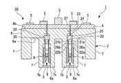
As shown in FIGS. 1 and 2, the heat dissipation structure 1 includes a
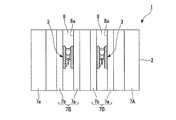
具体的に、この放熱構造1において、ヒートシンク2は、例えばCuやAlなどの熱伝導性の高い材料からなる。ヒートシンク2は、ベース部6と、複数の放熱フィン7A,7Bとを有している。ベース部6は、矩形平板状に形成されている。各放熱フィン7A,7Bは、矩形平板状に形成されて、ベース部6の第一の面6aに対して垂直に立設されている。また、複数の放熱フィン7A,7Bは、ベース部6の長手方向(図2中における左右方向)の両端部及びその両端部の間に位置して、互いに間隔を空けた状態で並んで設けられている。また、各放熱フィン7A,7Bは、ベース部6の短手方向(図2中における上下方向)の両端部の間に亘って立設されている。 Specifically, in this heat dissipation structure 1, the
本実施形態では、複数の放熱フィン7A,7Bのうち、ベース部6の長手方向の両端部に沿った位置に2つの放熱フィン7Aと、これら2つの放熱フィン7Aの間に2つの放熱フィン7Bとがベース部6の長手方向に並んで設けられている。また、放熱フィン7Bは、半導体モジュール3を配置するため、放熱フィン7Aよりも高さ及び厚み方向の寸法が大きくなっている。なお、ヒートシンク2については、本実施形態のものに必ずしも限定されるものではなく、各放熱フィン7A,7Bの数や寸法等を適宜変更して実施することが可能である。 In the present embodiment, among the plurality of heat radiation fins 7A and 7B, two heat radiation fins 7A are disposed at positions along both longitudinal ends of the
放熱フィン7Bには、差込溝8が設けられている。差込溝8は、放熱フィン7Bの先端側に設けられた差込口8aから半導体モジュール3を差し込み可能に保持する。具体的に、この差込溝8は、放熱フィン7Bの先端側から一定の幅で第一の面6aに対して垂直に半導体モジュール3を差し込むのに十分な深さで切り欠かれている。放熱フィン7Bは、この差込溝8によって2つのフィン部7a,7bに分断されている。
また、放熱フィン7Bには、差込口8aを塞ぐ蓋材9(図2において図示を省略する。)が設けられている。蓋材9は、差込溝8に半導体モジュール3が差し込まれた状態で、差込口8aを閉塞するように取り付けられている。なお、蓋材9の取付構造については、このような構造に必ずしも限定されるものではなく、放熱フィン7を差込溝8の幅方向から挟み込むように蓋材9が取り付けられた構造とすることが可能である。また、蓋材9については、省略することも可能である。 Further, the
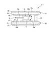
半導体モジュール3は、図3に拡大して示すように、第一の基板10と、第一の半導体素子11と、接続子12と、第二の半導体素子13と、第二の基板14とを、順に積層することにより構成されている。 As shown in an enlarged view in FIG. 3, the
このうち、第一及び第二の基板10,14は、セラミック基板であり、セラミック板(絶縁板)15,16と、セラミック板15,16の両面に設けられたCu層(導電層)17,18とを有している。また、第一の基板10と第二の基板14との互いに対向する面側のCu層17,18は、この半導体モジュール3の回路パターン17a,18aを形成している。なお、第一及び第二の基板10,14は、セラミック基板に限らず、例えばアルミニウム基板であってもよい。アルミニウム基板は、アルミニウム板の両面に絶縁層を介してCu層が設けられた構成である。 Among these, the first and
第一及び第二の半導体素子11,13は、動作時の発熱量が比較的大きい、例えばパワーダイオードやパワートランジスタなどのパワーデバイスである。第一の半導体素子11と第二の半導体素子13とは、第一の基板10と第二の基板14との互いに対向する面側に各々実装されることによって、それぞれの回路パターン17a,18aと電気的に接続されている。 The first and
接続子12は、例えばCuなどの導電性材料からなる。接続子12は、第一の接続部12aと、第二の接続部12bと、連結部12cとを有している。このうち、第一の接続部12aは、第一の半導体素子11と第二の半導体素子13とを電気的に接続する部分であり、第二の接続部12bは、一方の回路パターン17aと電気的に接続される部分であり、連結部12cは、第一の接続部12aと第二の接続部12bとを連結する部分である。 The
第一の接続部12aは、第一の基板10と第二の基板14との間隔を保持するのに十分な厚みで柱状に形成されている。第一の接続部12aの両端部は、はんだ等の導電性接着剤(図示せず。)を介して第一の半導体素子11及び第二の半導体素子13と接合されている。第二の接続部12bは、板状に形成されて、はんだ等の導電性接着剤(図示せず。)を介して一方の回路パターン17aと接合されている。連結部12cは、第一の接続部12aと第二の接続部12bとを連結するのに十分な長さで長尺板状に形成されている。連結部12cの一端側は、第一の接続部12aの側面と一体に接続されている。連結部12cの他端側は、第二の接続部12b側に折り曲げられて第二の接続部12bと一体に接続されている。 The
第一の基板10と第二の基板14との間には、スペーサ19が配置されている。スペーサ19は、第一の接続部12aと共に、第一の基板10と第二の基板14との間隔を保持している。また、スペーサ19は、この半導体モジュール3の回路部品として、回路パターン17a,18aの間に挟み込まれた状態で配置されている。回路部品としては、例えば、配線部、抵抗器、コンデンサなどが挙げられる。 A
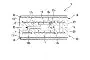
図1及び図2に示す回路基板4及び複数の電子部品5は、半導体モジュール3の駆動を制御する制御部30を構成している。このうち、回路基板4は、ヒートシンク2(ベース部6)の第一の面6aとは反対側の第二の面6bに接合されている。一方、複数の電子部品5は、回路基板4上に実装されている。各電子部品5は、各半導体モジュール3よりも発熱量が小さい発熱部品である。 The circuit board 4 and the plurality of
複数の電子部品5のうち一部の電子部品5と半導体モジュール3とは、コネクタ20を介して電気的に接続されている。コネクタ20は、半導体モジュール3側の第一の接続端子21a,21bが差し込まれる第一の差込口22a,22bと、電子部品5側の第二の接続端子23が差し込まれる第二の差込口24とを有している。半導体モジュール3側の第一の接続端子21a,21bは、図3において図示を省略するものの、回路パターン17a,18aと各々接続されている。 Some of the plurality of
ヒートシンク2には、コネクタ20を差し込み可能に保持する差込孔25が設けられている。ヒートシンク2には、半導体モジュール3側の第一の接続端子21a,21bを貫通させる第一の貫通孔26a,26bが設けられている。第一の貫通孔26a,26bは、差込溝8の底面から差込孔25に向かって形成されている。ヒートシンク2及び回路基板4には、電子部品5側の第二の接続端子23を貫通させる第二の貫通孔27が設けられている。第二の貫通孔27は、回路基板4の電子部品5が実装される面から差込孔25に向かって形成されている。また、第一の接続端子21a,21b及び第二の接続端子23は、第一の貫通孔26a,26b及び第二の貫通孔27との間で電気的に絶縁されている。 The
以上のような構成を有する放熱構造1では、半導体モジュール3が差込溝8に差し込まれた状態で放熱フィン7Bと接している。これにより、半導体モジュール3が発する熱は、差込溝8の内壁面、すなわちフィン部7a,7bと接する第一及び第二の基板10,14から放熱フィン7Bへと伝わり、外部に放熱されることになる。一方、複数の電子部品5が発する熱は、回路基板4からベース部6を経由して放熱フィン7A,7Bへと伝わり、外部に放熱されることになる。この場合、半導体モジュール3が発する熱は、ベース部6を経由することなく、放熱フィン7Bへと直接伝わるため、熱の伝達経路が短くなり、半導体モジュール3の放熱性が高まる。 In the heat dissipation structure 1 having the above-described configuration, the
以上のように、本実施形態の放熱構造1では、半導体モジュール3を放熱フィン7Bに接した状態で配置することで、従来のように半導体モジュール3をベース部6の第二の面6bに配置する場合に比べて、高い放熱性を得ることが可能である。 As described above, in the heat dissipation structure 1 of the present embodiment, the
また、本実施形態の放熱構造1では、半導体モジュール3を差込溝8に差し込んだ状態で配置することで、従来のように半導体モジュール3をベース部6の第二の面6bに配置する場合に比べて、小型化が可能となる。さらに、半導体モジュール3の第一及び第二の基板10,14をフィン部7a,7bに接触させることで、半導体モジュール3からの放熱を効率よく行わせることが可能である。 Further, in the heat dissipation structure 1 of the present embodiment, the
ところで、半導体モジュール3については、図4Aに模式的に示すように、絶縁性の確保及びパーティクルに対する保護のため、モールド樹脂28によって第一の基板10と第二の基板14との互いに対向する面側を封止することが行われる。しかしながら、このようなモールド樹脂28は、第一及び第二の半導体素子11,13や第一及び第二の基板10,14等との間で線膨張係数の差が大きいため、熱膨張時にクラック等が生じ易い。 By the way, as shown schematically in FIG. 4A for the
これに対して、本発明では、図4Bに模式的に示すように、モールド樹脂28の代わりに、第一の基板10と第二の基板14との互いに対向する面を覆う絶縁膜29を設けた構成とすることが可能である。絶縁膜29には、例えばセラミック等の高熱伝導性を有する絶縁材料が用いられる。 On the other hand, in the present invention, as schematically shown in FIG. 4B, an insulating
本実施形態の放熱構造1では、このような絶縁膜29が設けられた半導体モジュール3を差込溝8に差し込むことによって、絶縁性の確保及びパーティクルに対する保護が可能となる。さらに、絶縁膜29を設けた場合は、絶縁膜29の薄膜化によって半導体モジュール3からの放熱性が高められるだけでなく、線膨張係数の差によるクラックの発生が抑制可能となる。また、モールド樹脂28で封止するための工程が省略できるため、製造工程の簡略化が図れる。 In the heat dissipation structure 1 of the present embodiment, it is possible to ensure insulation and protect against particles by inserting the
なお、本発明は、上記実施形態のものに必ずしも限定されるものではなく、本発明の趣旨を逸脱しない範囲において種々の変更を加えることが可能である。
具体的に、本発明では、上述した差込溝8に半導体モジュール3が差し込まれた構成に必ずしも限定されるものではなく、半導体モジュール3が複数の放熱フィン7A,7Bのうちの少なくとも1つの放熱フィン7A(7B)と接する構成であればよい。In addition, this invention is not necessarily limited to the thing of the said embodiment, A various change can be added in the range which does not deviate from the meaning of this invention.
Specifically, the present invention is not necessarily limited to the configuration in which the
したがって、例えば、図5Aに示すように、隣り合う放熱フィン7の間に半導体モジュール3が挟み込まれた構成や、図5Bに示すように、放熱フィン7の一側面に半導体モジュール3が接した構成とすることも可能である。また、半導体モジュール3は、上述した放熱フィン7を挟んで対向して配置された構成に限らず、図5Cに示すように、放熱フィン7を挟んで配置をずらした構成とすることも可能である。 Therefore, for example, as shown in FIG. 5A, a configuration in which the
また、本発明の第一の発熱部品としては、上述した半導体モジュール3に必ずしも限定されるものではなく、その配置される位置や数等についても適宜変更を加えることが可能である。また、差込溝8についても、第一の発熱部品の大きさに合わせて適宜変更を加えることが可能である。したがって、複数の放熱フィン7には、個々の第一の発熱部品の大きさに合わせて深さや幅の異なる差込溝8が設けられていてもよい。 In addition, the first heat generating component of the present invention is not necessarily limited to the
また、本発明は、上述した差込溝8の差込口を塞ぐ蓋材9が設けられた構成に限らず、上述した差込孔25のように、半導体モジュール3を差し込み可能に保持する差込孔が設けられた構成としてもよい。 In addition, the present invention is not limited to the configuration in which the lid member 9 that closes the insertion port of the
また、本発明では、例えば図6Aに示すように、差込溝8に半導体モジュール3を差し込み易くするため、差込口8aにテーパー部8bを設けた構成としてもよい。また、差込溝8については、上述した一定の幅を有する形状に限らず、例えば図6Bに示すように、深さ方向の先端部に向かって漸次幅が狭くなる形状(いわゆる楔形状)や、図6Cに示すように、深さ方向の中央部に向かって漸次幅が狭くなる形状(いわゆる鼓形状)とすることで、この差込溝8に差し込まれた半導体モジュール3が容易に抜けない構造とすることも可能である。また、放熱膨張時に半導体モジュール3がフィン部7a,7bに密着することで、放熱性を高めることが可能である。 Further, in the present invention, for example, as shown in FIG. 6A, in order to make it easy to insert the
1…放熱構造 2…ヒートシンク 3…半導体モジュール(第一の発熱部品) 4…回路基板 5…電子部品(第二の発熱部品) 6…ベース部 6a…第一の面 6b…第二の面 7A,7B…放熱フィン 7a,7b…フィン部 8…差込溝 9…蓋材 10…第一の基板 11…第一の半導体素子 12…接続子 13…第二の半導体素子 14…第二の基板 15,16…セラミック板(絶縁板) 17,18…Cu層(導電層) 17a,18a…回路パターン 19…スペーサ 20…コネクタ 21a,21b…第一の接続端子 22a,22b…第一の差込口 23…第二の接続端子 24…第二の差込口 25…差込孔 26a,26b…第一の貫通孔 27…第二の貫通孔 28…モールド樹脂 29…絶縁膜 30…制御部 DESCRIPTION OF SYMBOLS 1 ...
Claims (9)
Translated fromJapanese前記差込口から前記差込溝に差し込まれ、前記第一と第二のフィン部の少なくとも1つと接する第一の発熱部品と、
前記ベース部の前記第二の面に接合され、前記第一の発熱部品と電気的に接続された回路基板と、
を含み、
前記差込溝の側面がテーパー形状を有している
放熱構造。A heat sink including a base portion having first and second surfaces facing each other and at least one heat radiating fin extending perpendicularly from the first surface, wherein each heat radiating fin is at a tip thereof. A heat sink having an insertion groove extending from the insertion port toward the base portion, and first and second fin portions divided by the insertion groove;
A first heat generating component that is inserted into the insertion groove from the insertion port and is in contact with at least one of the first and second fin portions;
A circuit board joined to the second surface of the base portion and electrically connected to the first heat-generating component;
Including
A heat dissipation structure in which a side surface of the insertion groove has a tapered shape.
前記差込口は、前記ベース部から前記差込口に向かって漸次幅が広くなるテーパー形状を有している請求項2または請求項3に記載の放熱構造。The tip portions of the first and second fin portions are curved,
The heat dissipation structure according to claim 2 or 3, wherein the insertion port has a tapered shape in which a width gradually increases from the base portion toward the insertion port.
を更に含む請求項1に記載の放熱構造。The heat dissipation structure according to claim 1, further comprising: a second heat generating component that is on the circuit board and has a heat generation amount smaller than that of the first heat generating component.
を更に含む請求項1に記載の放熱構造。The heat dissipation structure according to claim 1, further comprising: a lid member that closes the insertion port.
前記第一の基板および前記第二の基板が、それぞれ前記第一と第二のフィン部と接している
請求項1に記載の放熱構造。The first heat-generating component includes a first substrate, a first semiconductor element, a connector, a second semiconductor element, and a second substrate, which are sequentially stacked.
The heat dissipation structure according to claim 1, wherein the first substrate and the second substrate are in contact with the first and second fin portions, respectively.
を更に含む請求項7に記載の放熱構造。The heat dissipation structure according to claim 7, further comprising a protective film that covers surfaces of the first substrate and the second substrate facing each other.
を更に含む請求項5に記載の放熱構造。6. The connector according to claim 5, further comprising a connector that is in the base portion and is on the insertion groove in a plan view and detachably electrically connects the first heat generating component and the second heat generating component. Heat dissipation structure.
Applications Claiming Priority (1)
| Application Number | Priority Date | Filing Date | Title |
|---|---|---|---|
| PCT/JP2014/078771WO2016067390A1 (en) | 2014-10-29 | 2014-10-29 | Heat-dissipating structure |
Publications (2)
| Publication Number | Publication Date |
|---|---|
| JP6091035B2true JP6091035B2 (en) | 2017-03-15 |
| JPWO2016067390A1 JPWO2016067390A1 (en) | 2017-04-27 |
Family
ID=55856776
Family Applications (1)
| Application Number | Title | Priority Date | Filing Date |
|---|---|---|---|
| JP2015554912AActiveJP6091035B2 (en) | 2014-10-29 | 2014-10-29 | Heat dissipation structure |
Country Status (2)
| Country | Link |
|---|---|
| JP (1) | JP6091035B2 (en) |
| WO (1) | WO2016067390A1 (en) |
Families Citing this family (2)
| Publication number | Priority date | Publication date | Assignee | Title |
|---|---|---|---|---|
| JP6696837B2 (en)* | 2016-06-10 | 2020-05-20 | 古河電気工業株式会社 | Heat dissipation structure for heat generating parts |
| KR20220159950A (en)* | 2020-03-26 | 2022-12-05 | 덴카 주식회사 | Ceramic circuit board, heat dissipation member and aluminum-diamond composite |
Citations (7)
| Publication number | Priority date | Publication date | Assignee | Title |
|---|---|---|---|---|
| JPH1051912A (en)* | 1996-08-01 | 1998-02-20 | Hitachi Ltd | Electric device having radiating fins |
| US20050099779A1 (en)* | 2003-11-12 | 2005-05-12 | Toshiba International Corporation | Locking heatsink apparatus |
| WO2005091692A1 (en)* | 2004-03-18 | 2005-09-29 | Mitsubishi Denki Kabushiki Kaisha | Module heat radiation structure and control device using the same |
| JP2008282931A (en)* | 2007-05-09 | 2008-11-20 | Fujitsu Ten Ltd | Electric circuit device |
| JP2010129801A (en)* | 2008-11-28 | 2010-06-10 | Mitsubishi Electric Corp | Power semiconductor device |
| JP2011103395A (en)* | 2009-11-11 | 2011-05-26 | Sumitomo Electric Ind Ltd | Heat radiating structure of heat generating component and circuit device including the same heat radiating structure |
| US20110286179A1 (en)* | 2010-05-24 | 2011-11-24 | International Business Machines Corporation | Memory module connector having memory module cooling structures |
Family Cites Families (7)
| Publication number | Priority date | Publication date | Assignee | Title |
|---|---|---|---|---|
| JP2570832Y2 (en)* | 1992-02-28 | 1998-05-13 | 日本電気株式会社 | Heat sink for semiconductor |
| JP3565152B2 (en)* | 2000-09-26 | 2004-09-15 | 株式会社ノーリツ | Heat dissipation member |
| JP3935381B2 (en)* | 2002-03-14 | 2007-06-20 | 松下電器産業株式会社 | Electronic circuit device having double-sided electrode semiconductor element and method of manufacturing the electronic circuit device |
| JP2010187504A (en)* | 2009-02-13 | 2010-08-26 | Mitsubishi Electric Corp | Inverter device |
| JP2011114176A (en)* | 2009-11-27 | 2011-06-09 | Mitsubishi Electric Corp | Power semiconductor device |
| JP2014154391A (en)* | 2013-02-08 | 2014-08-25 | Denso Corp | Light emitting device |
| WO2014132425A1 (en)* | 2013-02-28 | 2014-09-04 | 新電元工業株式会社 | Electronic module and production method for same |
- 2014
- 2014-10-29WOPCT/JP2014/078771patent/WO2016067390A1/enactiveApplication Filing
- 2014-10-29JPJP2015554912Apatent/JP6091035B2/enactiveActive
Patent Citations (7)
| Publication number | Priority date | Publication date | Assignee | Title |
|---|---|---|---|---|
| JPH1051912A (en)* | 1996-08-01 | 1998-02-20 | Hitachi Ltd | Electric device having radiating fins |
| US20050099779A1 (en)* | 2003-11-12 | 2005-05-12 | Toshiba International Corporation | Locking heatsink apparatus |
| WO2005091692A1 (en)* | 2004-03-18 | 2005-09-29 | Mitsubishi Denki Kabushiki Kaisha | Module heat radiation structure and control device using the same |
| JP2008282931A (en)* | 2007-05-09 | 2008-11-20 | Fujitsu Ten Ltd | Electric circuit device |
| JP2010129801A (en)* | 2008-11-28 | 2010-06-10 | Mitsubishi Electric Corp | Power semiconductor device |
| JP2011103395A (en)* | 2009-11-11 | 2011-05-26 | Sumitomo Electric Ind Ltd | Heat radiating structure of heat generating component and circuit device including the same heat radiating structure |
| US20110286179A1 (en)* | 2010-05-24 | 2011-11-24 | International Business Machines Corporation | Memory module connector having memory module cooling structures |
Also Published As
| Publication number | Publication date |
|---|---|
| JPWO2016067390A1 (en) | 2017-04-27 |
| WO2016067390A1 (en) | 2016-05-06 |
Similar Documents
| Publication | Publication Date | Title |
|---|---|---|
| WO2016067383A1 (en) | Heat-dissipating structure | |
| JP6027945B2 (en) | Electronic control unit | |
| CN106057752A (en) | Semiconductor device and method for manufacturing semiconductor device | |
| WO2018146933A1 (en) | Semiconductor device and method for manufacturing semiconductor device | |
| JP6552450B2 (en) | Semiconductor device | |
| JP6249931B2 (en) | Circuit board, circuit board heat dissipation structure, and circuit board manufacturing method | |
| CN109196637B (en) | Semiconductor device with a plurality of semiconductor chips | |
| CN107251669A (en) | Base board unit | |
| JP5670447B2 (en) | Electronics | |
| JP6330053B2 (en) | Heat dissipation structure | |
| JP6091035B2 (en) | Heat dissipation structure | |
| JP5717922B1 (en) | Power converter | |
| JP6336106B2 (en) | Heat dissipation structure | |
| JP2014135374A (en) | Heat transfer substrate | |
| JP6686467B2 (en) | Electronic component heat dissipation structure | |
| JP6200693B2 (en) | Electronic control unit | |
| JP6265260B2 (en) | Power module | |
| JP2011171686A (en) | Metal-based printed board with heat radiation part | |
| JP2015216143A (en) | Heat dissipation structure | |
| JP2020047690A (en) | Electronic circuit device | |
| JP2016152290A (en) | Thermal conductive substrate and method for mounting electronic component | |
| JP2017011027A (en) | Heat dissipation structure for circuit board | |
| JP2014049728A (en) | Circuit device | |
| JP2012190944A (en) | Semiconductor device |
Legal Events
| Date | Code | Title | Description |
|---|---|---|---|
| A529 | Written submission of copy of amendment under article 34 pct | Free format text:JAPANESE INTERMEDIATE CODE: A5211 Effective date:20151105 | |
| A621 | Written request for application examination | Free format text:JAPANESE INTERMEDIATE CODE: A621 Effective date:20151105 | |
| TRDD | Decision of grant or rejection written | ||
| A01 | Written decision to grant a patent or to grant a registration (utility model) | Free format text:JAPANESE INTERMEDIATE CODE: A01 Effective date:20170110 | |
| A61 | First payment of annual fees (during grant procedure) | Free format text:JAPANESE INTERMEDIATE CODE: A61 Effective date:20170206 | |
| R150 | Certificate of patent or registration of utility model | Ref document number:6091035 Country of ref document:JP Free format text:JAPANESE INTERMEDIATE CODE: R150 |