JP6085630B2 - Touch pen system and touch pen - Google Patents
Touch pen system and touch penDownload PDFInfo
- Publication number
- JP6085630B2 JP6085630B2JP2015047712AJP2015047712AJP6085630B2JP 6085630 B2JP6085630 B2JP 6085630B2JP 2015047712 AJP2015047712 AJP 2015047712AJP 2015047712 AJP2015047712 AJP 2015047712AJP 6085630 B2JP6085630 B2JP 6085630B2
- Authority
- JP
- Japan
- Prior art keywords
- pen
- touch
- touch pen
- predetermined
- rear end
- Prior art date
- Legal status (The legal status is an assumption and is not a legal conclusion. Google has not performed a legal analysis and makes no representation as to the accuracy of the status listed.)
- Active
Links
Images


Classifications
- G—PHYSICS
- G06—COMPUTING OR CALCULATING; COUNTING
- G06F—ELECTRIC DIGITAL DATA PROCESSING
- G06F3/00—Input arrangements for transferring data to be processed into a form capable of being handled by the computer; Output arrangements for transferring data from processing unit to output unit, e.g. interface arrangements
- G06F3/01—Input arrangements or combined input and output arrangements for interaction between user and computer
- G06F3/03—Arrangements for converting the position or the displacement of a member into a coded form
- G06F3/033—Pointing devices displaced or positioned by the user, e.g. mice, trackballs, pens or joysticks; Accessories therefor
- G06F3/0354—Pointing devices displaced or positioned by the user, e.g. mice, trackballs, pens or joysticks; Accessories therefor with detection of 2D relative movements between the device, or an operating part thereof, and a plane or surface, e.g. 2D mice, trackballs, pens or pucks
- G06F3/03545—Pens or stylus
- G—PHYSICS
- G06—COMPUTING OR CALCULATING; COUNTING
- G06F—ELECTRIC DIGITAL DATA PROCESSING
- G06F3/00—Input arrangements for transferring data to be processed into a form capable of being handled by the computer; Output arrangements for transferring data from processing unit to output unit, e.g. interface arrangements
- G06F3/01—Input arrangements or combined input and output arrangements for interaction between user and computer
- G06F3/03—Arrangements for converting the position or the displacement of a member into a coded form
- G06F3/033—Pointing devices displaced or positioned by the user, e.g. mice, trackballs, pens or joysticks; Accessories therefor
- G06F3/039—Accessories therefor, e.g. mouse pads
- G06F3/0393—Accessories for touch pads or touch screens, e.g. mechanical guides added to touch screens for drawing straight lines, hard keys overlaying touch screens or touch pads
- G—PHYSICS
- G06—COMPUTING OR CALCULATING; COUNTING
- G06F—ELECTRIC DIGITAL DATA PROCESSING
- G06F3/00—Input arrangements for transferring data to be processed into a form capable of being handled by the computer; Output arrangements for transferring data from processing unit to output unit, e.g. interface arrangements
- G06F3/01—Input arrangements or combined input and output arrangements for interaction between user and computer
- G06F3/03—Arrangements for converting the position or the displacement of a member into a coded form
- G06F3/041—Digitisers, e.g. for touch screens or touch pads, characterised by the transducing means
- G06F3/044—Digitisers, e.g. for touch screens or touch pads, characterised by the transducing means by capacitive means
- G06F3/0442—Digitisers, e.g. for touch screens or touch pads, characterised by the transducing means by capacitive means using active external devices, e.g. active pens, for transmitting changes in electrical potential to be received by the digitiser
- G—PHYSICS
- G06—COMPUTING OR CALCULATING; COUNTING
- G06F—ELECTRIC DIGITAL DATA PROCESSING
- G06F2203/00—Indexing scheme relating to G06F3/00 - G06F3/048
- G06F2203/048—Indexing scheme relating to G06F3/048
- G06F2203/04808—Several contacts: gestures triggering a specific function, e.g. scrolling, zooming, right-click, when the user establishes several contacts with the surface simultaneously; e.g. using several fingers or a combination of fingers and pen
Landscapes
- Engineering & Computer Science (AREA)
- General Engineering & Computer Science (AREA)
- Theoretical Computer Science (AREA)
- Human Computer Interaction (AREA)
- Physics & Mathematics (AREA)
- General Physics & Mathematics (AREA)
- Position Input By Displaying (AREA)
Description
Translated fromJapanese本発明は、タッチペンシステム及びタッチペンに関する。 The present invention relates to a touch pen system and a touch pen.
タッチパネルは、携帯型情報機器(タブレット、ノートPC、スマートフォン、携帯電話、PDA等)、デジタルオーディオプレーヤー、携帯ゲーム機、カーナビゲーション装置、コピー機、金融機関のATM、及び駅や飲食店の自動券売機など多方面に利用されている。このようなタッチパネルの操作は、画像が表示されるディスプレイ表面の所望の位置を、指、タッチペンやスタイラスなどと呼ばれる専用のペン(以下、「タッチペン」と称す。)でタッチ又は押圧することにより行う。 Touch panels are portable information devices (tablets, notebook PCs, smartphones, mobile phones, PDAs, etc.), digital audio players, portable game machines, car navigation devices, photocopiers, ATMs at financial institutions, and automatic ticket sales at stations and restaurants. It is used in many areas such as aircraft. Such a touch panel operation is performed by touching or pressing a desired position on the display surface on which an image is displayed with a dedicated pen called a finger, a touch pen, a stylus, or the like (hereinafter referred to as a “touch pen”). .
タッチパネルには、抵抗膜方式、表面弾性波方式、赤外線方式、電磁誘導方式、静電容量方式などがある。ここで、静電容量方式のタッチパネルでは、指先あるいはペンと導電膜との間で静電容量の変化を捉えることで、ディスプレイ上の入力位置を検出する。 The touch panel includes a resistance film method, a surface acoustic wave method, an infrared method, an electromagnetic induction method, and a capacitance method. Here, in the capacitive touch panel, an input position on the display is detected by capturing a change in capacitance between the fingertip or the pen and the conductive film.
かかる静電容量方式のタッチパネルに用いるタッチペンは、パッシブペンとアクティブペンがある。パッシブペンは、一般的に、ペンホルダーと、このペンホルダーの先端に取り付けられた、導電性ゴム等の柔らかい材質のペン先とから主に構成される。 Touch pens used for such capacitive touch panels include passive pens and active pens. Generally, a passive pen is mainly composed of a pen holder and a pen tip made of a soft material such as conductive rubber attached to the tip of the pen holder.
他方、アクティブペンは、主として、ペンホルダーと、このペンホルダーの先端に取り付けられたペン先と、ペン先から電界を発生させる、ペンホルダーの内部に設けられた電気回路とで構成されている。アクティブペンでは、ペン先から電界を発生させるため、タッチパネルでの位置検出精度が比較的よく、ペン先を細くすることができる。 On the other hand, the active pen mainly includes a pen holder, a pen tip attached to the tip of the pen holder, and an electric circuit provided inside the pen holder that generates an electric field from the pen tip. In the active pen, an electric field is generated from the pen tip, so that the position detection accuracy on the touch panel is relatively good, and the pen tip can be made thin.
また、近時、イレース機能を備えたタッチペンも提案されている。ここで、タッチペンの後端部にイレース機能を搭載する場合、後端部をアクティブ方式とすると、イレース機能用の電気回路が必要となるため、タッチペンが長くってしまい、また、コストが高くなってしまう。 Recently, a touch pen having an erase function has been proposed. Here, when the erase function is installed at the rear end of the touch pen, if the rear end is set to the active method, an electric circuit for the erase function is required, which increases the length of the touch pen and increases the cost. End up.
本発明は、上記に鑑みてなされたものであり、イレース機能を搭載する場合に、コンパクトかつ低コストな構成でタッチペンを構成することが可能なタッチペンシステム及びタッチペンを提供することを目的とする。 The present invention has been made in view of the above, and an object of the present invention is to provide a touch pen system and a touch pen capable of configuring a touch pen with a compact and low-cost configuration when an erase function is installed.
上述した課題を解決し、目的を達成するために、本発明は、静電容量型のタッチパネルと、前記タッチパネル上の任意の位置を指示するためのペン先と、所定の導電性パターンが形成されたペン後端部とを有するタッチペンと、前記タッチパネルに対する前記所定の導電性パターンの接触を検出する所定パターン検出手段と、前記所定の導電性パターンを検出した場合に、イレース機能を実行するイレース機能実行手段と、を備えたことを特徴とする。 In order to solve the above-described problems and achieve the object, the present invention includes a capacitive touch panel, a pen tip for indicating an arbitrary position on the touch panel, and a predetermined conductive pattern. A touch pen having a pen rear end, a predetermined pattern detecting means for detecting contact of the predetermined conductive pattern with the touch panel, and an erase function for executing an erase function when the predetermined conductive pattern is detected And an execution means.
また、本発明の好ましい態様によれば、前記所定の導電性パターンは、互いに所定の距離だけ離間した複数の導電性パターンであることが望ましい。 According to a preferred aspect of the present invention, it is desirable that the predetermined conductive pattern is a plurality of conductive patterns separated from each other by a predetermined distance.
また、本発明の好ましい態様によれば、前記所定の距離をL、前記タッチパネルの電極間の距離をPとした場合、前記所定の距離L≧2Pであることが望ましい。 Further, according to a preferred aspect of the present invention, when the predetermined distance is L and the distance between the electrodes of the touch panel is P, it is desirable that the predetermined distance L ≧ 2P.
また、本発明の好ましい態様によれば、前記ペン後端部は、斜面形状の端面を有し、前記所定の導電性パターンは、斜面形状の端面に形成されていることが望ましい。 Further, according to a preferred aspect of the present invention, it is desirable that the pen rear end portion has an inclined end surface, and the predetermined conductive pattern is formed on the inclined end surface.
また、本発明の好ましい態様によれば、前記イレース機能実行手段は、前記複数の導電性パターンが所定の間隔を維持した状態で所定距離移動するのを検出した場合に、イレース機能を実行することが望ましい。 According to a preferred aspect of the present invention, the erase function execution means executes the erase function when it is detected that the plurality of conductive patterns move a predetermined distance while maintaining a predetermined interval. Is desirable.
上述した課題を解決し、目的を達成するために、本発明は、静電容量型のタッチパネルで使用されるタッチペンであって、前記タッチパネル上の任意の位置を指示するためのペン先と、所定の導電性パターンが形成されたペン後端部と、を備え、前記ペン後端部には、所定の導電性パターンが形成されていることが望ましい。 In order to solve the above-described problems and achieve the object, the present invention is a touch pen used in a capacitive touch panel, a pen tip for indicating an arbitrary position on the touch panel, And a pen rear end portion on which the conductive pattern is formed, and a predetermined conductive pattern is preferably formed on the pen rear end portion.
また、本発明の好ましい態様によれば、前記所定の導電性パターンは、互いに所定の距離だけ離間した複数の導電性パターンであることが望ましい。 According to a preferred aspect of the present invention, it is desirable that the predetermined conductive pattern is a plurality of conductive patterns separated from each other by a predetermined distance.
また、本発明の好ましい態様によれば、前記所定の距離をL、前記タッチパネルの電極間の距離をPとした場合、前記所定の距離L≧2Pであることが望ましい。 Further, according to a preferred aspect of the present invention, when the predetermined distance is L and the distance between the electrodes of the touch panel is P, it is desirable that the predetermined distance L ≧ 2P.
また、本発明の好ましい態様によれば、前記ペン後端部は、斜面形状の端面を有し、前記所定の導電性パターンは、斜面形状の端面に形成されていることが望ましい。 Further, according to a preferred aspect of the present invention, it is desirable that the pen rear end portion has an inclined end surface, and the predetermined conductive pattern is formed on the inclined end surface.
本発明によれば、イレース機能を搭載する場合に、コンパクトかつ低コストな構成でタッチペンを構成することが可能なタッチペンシステム及びタッチペンを提供することが可能になるという効果を奏する。 According to the present invention, when the erase function is installed, it is possible to provide a touch pen system and a touch pen that can form a touch pen with a compact and low-cost configuration.
以下、本発明に係るタッチペンシステム及びタッチペンの実施の形態について説明する。本発明の構成要素は、本明細書の図面に一般に示してあるが、様々な構成で広く多様に配置し設計してもよいことは容易に理解できる。したがって、本発明のタッチペンシステム及びタッチペンの実施の形態についての以下のより詳細な説明は、特許請求の範囲に示す本発明の範囲を限定するものではなく、単に本発明の選択した実施の形態の一例を示すものであって、本明細書の特許請求の範囲に示す本発明と矛盾無く、装置、構成、構造についての選択した実施の形態を単に示すものである。当業者は、特定の細目の1つ以上が無くても、又は他の方法、部品、材料でも本発明を実現できることが理解できる。 Hereinafter, embodiments of a touch pen system and a touch pen according to the present invention will be described. Although the components of the present invention are generally illustrated in the drawings herein, it can be readily understood that they may be arranged and designed in a wide variety of configurations with various configurations. Accordingly, the following more detailed description of the touch pen system and touch pen embodiments of the present invention is not intended to limit the scope of the present invention as set forth in the claims, but is merely a selection of embodiments of the present invention. It is intended as an example only, and is merely illustrative of selected embodiments of apparatus, construction and structure consistent with the present invention as set forth in the claims herein. Those skilled in the art will appreciate that the present invention may be implemented without one or more of the specific details or with other methods, components, and materials.
図1及び図2は、本実施の形態に係るタッチペンシステムの概略構成を示す斜視図を示しており、図1は、タッチペンのペン先を使用する状態、図2は、タッチペンのペン後端部(イレーサ)を使用する状態を示している。図3は、図1のタブレット型コンピュータ10の概略の断面図、図4は、タッチペンのペン後端部の端面の概略の平面図を示している。 1 and 2 are perspective views showing a schematic configuration of the touch pen system according to the present embodiment. FIG. 1 shows a state where the pen tip of the touch pen is used, and FIG. 2 shows a pen rear end portion of the touch pen. This shows a state in which the (eraser) is used. 3 is a schematic cross-sectional view of the
図1及び図2に示すように、タッチペンシステム1は、タブレット型コンピュータ10と、タブレット型コンピュータ10に座標入力とイレースを行うためのタッチペン20と、を備えている。本実施の形態に係るタッチペンシステム1は、タッチペン20のアクティブ式のペン先によるペン入力、指による指入力(パッシブ方式)、タッチペン20のペン後端部によるイレース入力(パッシブ方式)を認識でき、これらを区別可能に構成されている。 As shown in FIGS. 1 and 2, the touch pen system 1 includes a
図1〜図3に示すように、タブレット型コンピュータ10は、前面側に、表示部14と表示部14上に重畳されたタッチセンサ13とで構成されるタッチパネル12が配置されている。タブレット型コンピュータ10は、略長方体である筐体11に、タッチパネル12の表示及び座標検出を制御する回路等の各種電子部品を搭載した基板15、表示部14、タッチセンサ13が収納されている。筐体11は、例えば合成樹脂や金属で構成することができる。タッチセンサ12は、筐体11の額縁と略同一平面上に配置されている。 As illustrated in FIGS. 1 to 3, the
タッチペン20は、ペン先がいわゆるアクティブ型のペンとなっており、後端がパッシブ型のイレーサとなっている。タッチペン20は、ペン本体30と、ペン本体30に取り付けられたペン先40と、ペン本体30に取り付けられたキャップ形状のペン後端部50とを備えている。例えば、ペン先40は金属芯で構成し、その表面をフェールトで形成することができる。タッチペン20は、ペン先40で座標入力が可能となっている。 The
図1、図2,及び図4に示すように、ペン後端部50は、略円形状の端面53に2つの導電性のパターン54a、54bが形成されている。2つの導電性のパターン54a、54bは、略円形状を呈しており、互いの中心位置乃至重心位置Cから所定距離L離間している。ペン後端部50は、ペン本体30に対して交換可能に形成されている。タッチペン20のペン後端部50でイレースが可能となっている。 As shown in FIGS. 1, 2, and 4, the pen
タッチセンサ13は、静電容量方式のタッチセンサであり、指示体の多点検出及び面検出が可能となっている。タッチセンサ13は、タッチペン20のペン後端部50により、イレース機能が実行可能に構成されている。タッチセンサ13は、X方向及びY方向にマトリクス状に複数配列された透明のX電極及びY電極を備えており、指等の指示体による静電容量の変化、及びタッチペン20のペン先40により発生する所定周波数の交流電界による静電容量の変化を検出することで、指又はタッチペン20等による座標入力が可能となっている。また、タッチセンサ13は、タッチペン20のペン後端部50の端面53に形成された導電性のパターン54a、54bを検出することで、タッチペン20のペン後端部50によりイレース機能が実行可能となっている。 The
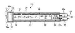
図5は、図1のタッチペン20の模式断面図を示している。図5に示すように、タッチペン20のペン本体30は、中空のシリンダーであるペン本体部21と、ペン本体部21に収容される基板22と、を備えている。ペン本体部21に、電源スイッチ31が設けられている。ペン本体部21は、導電性樹脂などの材料を用いてユーザが手で持って操作するのに好適な大きさ及び形状に形成されている。 FIG. 5 shows a schematic cross-sectional view of the
基板22には、ペン先40を摺動可能に保持するホルダー23と、バッテリ32、トランスデューサー33、コントロールIC34、圧力検出部35が搭載されている。ホルダー23はペン先40の挿入部40aが挿入され、ペン先40を外向きに付勢するスプリング23bを備えている。ペン先40は、ホルダー23に対して交換可能に形成されてもよい。 On the
圧力検出部35は、ペン先40がタッチパネル13などに当接され、その押圧力によってペン先40がスプリング23bの弾性力に抗して押し込まれた際の圧力を検出して、コントロールIC34に出力する。なお、圧力検出部35でペン先40の押下を検出することとしたが、これに限られるものではなく、他の公知の検出方法を使用してもよい。 The
バッテリ32は、例えば、リチウムイオン電池やアルカリイオン電池である。バッテリ32からコントロールIC34に電力が供給され、コントロールIC34は、電圧レベルを調整してトランスデューサー33及び圧力検出部35に電圧を供給する。トランスデューサー33は電圧が供給されると、発振を開始して正弦波信号を生成し、アクティブタッチペンとして用いられる。 The
トランスデューサー33は、例えば、電圧制御発振器であり、ペン先40の金属芯と電気的に接続されている。トランスデューサー33は、コントロールIC34により出力される電圧に基づいて正弦波信号(周波数f1,振幅A1)を生成し、正弦波信号をペン先40の金属芯を通じて送信し、タッチセンサ13を介して駆動検出部105(図6参照)がこれを受信する。 The
コントロールIC34は、圧力検出部35の圧力検出結果に基づいて、ペン先40の押下を検出した場合には、トランスデューサー33に出力する電圧を変更し、正弦波信号(周波数f2(但し、f2>f1),振幅A1)を生成させる。 When the
例えば、タッチペン20は、圧力検出部35で圧力が検出された場合にアクティブ状態とし、所定時間使用されない場合に、スリープ状態に移行するように構成してもよい。 For example, the
他方、ペン後端部50は、ペン本体部21に外嵌し、着脱可能に構成されたキャップ部52と、キャップ部52の円形状の端面53に形成された2つの導電性パターン54a、54bとを備えている。キャップ部52の側面は、例えば導電性樹脂で構成することができ、キャップ部52の端面53は、例えば絶縁性材料で構成することができる。図5に示す例では、ペン後端部50はペン本体部21に外嵌する例を示したが、ペン後端部50がペン本体21に内嵌するように構成してもよい。なお、導電性パターン54a、54bをタッチパネル12で検出できるように、例えば、ユーザがペン本体30を把持した時に、導電性パターン54a、54bと人体を導通可能に構成してもよく、また、導通しなくて、ペン本体部30にペイントを塗布して、接合容量によって動作可能としてもよい。 On the other hand, the pen
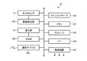
図6は、タブレット型コンピュータ10の概略のハードウェア構成例を示す図である。タブレット型コンピュータ10は、同図に示すように、メインコントローラ102、メモリ101、ストレージ103、I/F104、タッチセンサ13、駆動検出部105、表示部14、及びVRAM106、電源回路107、及び通信デバイス108等を備えており、各部はバスを介して直接または間接的に接続されている。 FIG. 6 is a diagram illustrating a schematic hardware configuration example of the
メインコントローラ102は、ストレージ103に格納されたプログラムに基づいて、タブレット型コンピュータ10全体の制御を行う。例えば、メインコントローラ102は、表示情報をVRAM106に格納して、VRAM106に格納した表示情報を表示部14に表示させる。また、メインコントローラ102は、駆動検出部105を介して、タッチセンサ13の動作を制御する。 The
メモリ103は、キャッシュメモリやRAMで構成されており、メインコントローラ102の実行プログラムの読み込み領域として、実行プログラムの処理データを書き込む作業領域として利用される書き込み可能メモリである。 The
ストレージ103は、例えば、SSD等の不揮発性メモリで構成することができ、メインコントローラ102が実行するためのプログラムを記憶する機能を有する。 The
VRAM106は、表示情報を格納するためのビットマップメモリである。表示部14は、例えば、LCD、有機EL等で構成されており、VRAM106に描画された表示情報を表示する。I/F104は、USB機器やBlue tooth(登録商標)機器を接続するための有線/無線のインターフェイスである。 The
通信デバイス108は、メインコントローラ102の制御に従って、ネットワークを介してデータの送受信を行うためのものである。 The
電源回路107は、ACアダプタ、インテリジェント電池、インテリジェント電池を充電するための充電器、およびDC/DCコンバータ等を備えており、メインコントローラ102の制御に従って、各部に電力を供給する。 The
タッチセンサ13は、ユーザが入力操作を行うためのユーザインターフェィスであり、ユーザが、表示部14の画面に表示される各種メニュー、アイコン、ボタン、およびキーボード等の画面オブジェクトを選択して入力操作を行ったり、テキストの入力操作や、スクロールやスワイプ等の画面操作を行うためのものである。タッチセンサ13は、ITOで構成されている、X方向及びY方向にマトリクス状に複数配列された透明のX電極X1,X2,...,Xn及びY電極Y1,Y2,...,Ynを備えている。The
駆動検出部105は、タッチセンサ103を駆動するためのドライブ回路やタッチ位置を検出するための検出回路を備え、メインコントローラ102の制御に従って、タッチセンサ12の動作をコントールする。駆動検出部105は、タッチセンサ13のX電極X1,X2,...,Xn及びY電極Y1,Y2,...,Ynに駆動信号を送出し、X電極X1,X2,...,Xn及びY電極Y1,Y2,...,Ynの出力を検出することによって、アクティブ方式のペン先40によるタッチと、パッシブ方式のタッチ(指や導電性パターン54a、54b等のタッチ)とを識別して、その識別信号と共に、タッチされたX電極及びY電極の座標位置(X、Y)をメインコントローラ102に出力する。The
例えば、駆動検出部105は、アクティブ方式のペン先40のタッチを検出した場合には、ペン入力モードを示す信号と、タッチされたX電極及びY電極の座標位置(X、Y)をメインコントローラ102に出力する。他方、駆動検出部105は、パッシブ方式のタッチ(指や導電性パターン54a、54b等のタッチ)を検出した場合には、パッシブモードを示す信号と、タッチされたX電極及びY電極の座標位置(X、Y)をメインコントローラ102に出力する。 For example, when the
駆動検出部105では、例えば、アクティブ方式のペン先では、タッチペン20のペン先40により発生する所定周波数の交流電界の変化を検出することで、アクティブ方式のペンがタッチされたと判定することができる(容量固定、印加電圧変化)。他方、パッシブ方式のタッチ(指や導電性パターン54a、54b等のタッチ)は、静電容量の変化を検出することでパッシブ方式のタッチを判定することができる(容量変化、印加電圧不変)。 In the
メインコントローラ102は、ペン入力モードと、指入力モードと、イレースモード(イレース機能)とを実行する。メインコントローラ102は、駆動検出部105からパッシブモードを示す信号と検出された座標位置(X,Y)が入力されると、検出された座標位置(X,Y)が、所定距離L離間した2つの導体パターン54a、54bに対応したものであるか否かを判断し、所定距離L離間した2つの導体パターン54a、54bに対応したものではない場合には、指入力モードを実行し、所定距離L離間した2つの導体パターン54a、54bに対応したものである場合には、イレースモードを実行する。 The
ペン入力モードでは、メインコントローラ102は、駆動検出部105で検出した座標位置(X,Y)に応じて、すなわち、ペン先40の軌跡に応じてVRAM106に表示情報を描画し、表示部14には、表示情報が表示される。例えば、メインコントローラ102は、ペン先40がタッチセンサ13にタッチされた場合に、カーソルを表示し、ペン先40をタッチセンサ12で押下した場合に、描画(筆記)を開始することにしてもよい。 In the pen input mode, the
イレースモードでは、メインコントローラ102は、VRAM106に描画されている表示情報のうち、駆動検出部105で検出した座標位置(X,Y)に応じて、すなわち、ペン後端部50の端面53の軌跡上のデータを消去する。ユーザは、タッチセンサ13にペン後端部50の端面53をタッチさせて、タッチパネル12上に表示されている描画情報をトレースすることで、描画情報をイレースすることができる。 In the erase mode, the
つぎに、図7及び図8を参照して、タッチペン20のペン後端部50の導電性パターン54a,54b間の距離L(上記図4参照)について説明する。図7及び図8は、X電極、Y電極の間隔と、2つの導電性パターン54a,54b間の距離Lとの関係を説明するための図である。図7及び図8において、X電極X1,X2,...,Xn間及びY電極Y1,Y2,...,Yn間の間隔をPとしている。図7は、2つの導電性パターン54a,54b間の距離L<2Pとした場合を示している。図8は、2つの導電性パターン54a,54b間の距離L≧2Pとした場合を示している。Next, a distance L (see FIG. 4) between the
2つの導電性パターン54a,54b間の距離Lは大きいほどタッチセンサ13で2つのパターンであることを高精度に検出できるため、距離Lを大きくするのが望ましい。他方、タッチペン20のペン後端部50の太さの関係で距離Lの大きさには制限がある。 As the distance L between the two
図7において、2つの導電性パターン54a,54b間の距離L<2Pとすると、2つのパターンであること検出できない可能性がある。例えば、X電極X3では、導電性パターン54a、54bの両方が重畳したものが検出されるため、2つのパターンを検出できない場合がある(例えば、指のタッチと区別できない)。In FIG. 7, if the distance L <2P between the two
他方、図8において、2つの導電性パターン54a,54b間の距離L≧2Pとすると、例えば、X電極X2,X3,X4,X5では、導電性パターン54a、54bの両方が重畳したものが検出されないため、2つのパターンを検出することができる。そのため、2つの導電性パターン54a,54b間の距離L≧2Pとすることが望ましい。On the other hand, in FIG. 8, assuming that the distance L ≧ 2P between the two
(変形例1)
図9は、タッチペンシステム1の変形例を説明するための図である。メインコントローラ102は、タッチセンサ13において、2つのパターンがそのパターン間の距離Lを維持したまま、所定距離Sの移動を検出した場合に、イレースを開始することにしてもよい。これにより、ユーザの意図に反して、間隔Lで2つの導電体をタッチしてしまった場合にイレースモードとなることを防止でき、イレースモードに移行するための精度を向上させることが可能となる。(Modification 1)
FIG. 9 is a diagram for explaining a modification of the touch pen system 1. The
(変形例2)
図10は、タッチペン20の変形例を説明するための図である。2つの導電性パターン54a,54b間の距離Lは大きいほどタッチセンサ13で2つのパターンであることを高精度に検出できる。そこで、例えば、図10に示すように、タッチペン20のペン後端部50の端面53を斜面状に形成してもよい。これにより、ペン後端部50を太くすることなく、距離Lを大きくすることが可能となる。(Modification 2)
FIG. 10 is a diagram for explaining a modification of the
(変形例3)
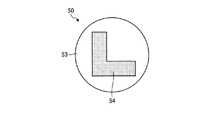
図11及び図12は、タッチペン20の変形例を説明するための図である。タッチペン20のペン後端部50の端面53に形成する導電性パターンは、図4等に示す2つの導電性パターン54a、54bに限られるものではなく、例えば、他の形状の導電性パターンとしてもよく、また、形成する導電性パターンの数を3つ以上としてもよい。例えば、図11に示すように、ドーナッツ状の導電性パターン54としてもよい。また、図12に示すように、L字状の導電性パターン54としてもよい。(Modification 3)
11 and 12 are diagrams for explaining a modification of the
以上説明したように、本実施の形態のタッチペンシステム1によれば、静電容量型のタッチパネル12と、タッチパネル12上の任意の位置を指示するためのペン先40及び所定の導電性パターンが形成されたペン後端部50を有するタッチペン20と、タッチパネル12に対する所定の導電性パターンの接触を検出し、所定の導電性パターンを検出した場合に、イレース機能を実行する駆動検出部105及びメインコントローラ102とを備えているので、イレース機能を搭載する場合に、コンパクトかつ低コストな構成でタッチペンを構成することが可能となる。 As described above, according to the touch pen system 1 of the present embodiment, the
また、本実施の形態によれば、所定の導電性パターンは、互いに所定の距離だけ離間した複数の導電性パターン54a、54bとしたので、高精度に所定の導電性パターンを検出することが可能となる。 In addition, according to the present embodiment, the predetermined conductive pattern is a plurality of
また、本発明の形態によれば、導電性パターン54a、54b間の距離を所定の距離L、タッチパネル12の電極間の距離をPとした場合、所定の距離L≧2Pとしたので、より高精度に所定の導電性パターンを検出することが可能となる。 Further, according to the embodiment of the present invention, when the distance between the
また、本発明の形態によれば、ペン後端部50は、斜面形状の端面53を有し、導電性パターン54a、54bを、斜面形状の端面53に形成することとしたので、ペン後端部50を太くすることなく、導電性パターン54a、54b間の距離Lを大きくすることが可能となる。 In addition, according to the embodiment of the present invention, the pen
また、本発明の形態によれば、メインコントローラ102は、複数の導電性パターンが所定の間隔Lを維持した状態で所定距離S移動するのを検出した場合に、イレース機能を実行することとしたので、ユーザの意図に反してイレース機能が実行されるのを防止することが可能となる。 Further, according to the embodiment of the present invention, the
なお、本実施の形態では、ペン入力(ペン先40)をアクティブ方式としているが、パッシブ方式を使用することにしてもよい。 In the present embodiment, the pen input (pen tip 40) is an active method, but a passive method may be used.
1 タッチペンシステム
10 タブレット型コンピュータ
11 筐体
12 タッチパネル
13 タッチセンサ
14 表示部
20 タッチペン
21 ペン本体部
22 基板
23 ホルダー
23b スプリング
30 ペン本体
32 バッテリ
33 トランスデューサー
34 コントロールIC
35 圧力検出部
40 ペン先
50 ペン後端部
52 キャップ部
53 端面
54a、54b 導電性パターン
101 メモリ
102 メインコントローラ
103 ストレージ
104 I/F
105 駆動検出部
106 VRAM
107 電源回路
108 通信デバイスDESCRIPTION OF SYMBOLS 1
DESCRIPTION OF
35
105
107
Claims (9)
Translated fromJapanese前記タッチパネル上の任意の位置を指示するためのアクティブ式のペン先と、絶縁性材料で構成される端面と略面一に所定形状の導電性パターンが形成されたパッシブ式のペン後端部とを有するタッチペンと、
前記タッチパネルに対する前記所定形状の導電性パターンの接触を検出する所定パターン検出手段と、
前記所定形状の導電性パターンを検出した場合に、イレース機能を実行するイレース機能実行手段と、
を備えたことを特徴とするタッチペンシステム。A capacitive touch panel;
Anactive pen tip for indicating an arbitrary position on the touch panel, and apassive pen rear end portion having a conductive pattern having apredetermined shape substantially flush with an end face made of aninsulating material, A touch pen having
Predetermined pattern detecting means for detecting contact of the conductive pattern of the predeterminedshape with the touch panel;
An erase function executing means for executing an erase function when detecting the conductive pattern of the predeterminedshape ;
A touch pen system characterized by comprising:
前記タッチパネル上の任意の位置を指示するためのアクティブ式のペン先と、
絶縁性材料で構成される端面と略面一に所定形状の導電性パターンが形成されたパッシブ式のペン後端部と、
を備え、
前記ペン後端部は、所定形状の導電性パターンが形成されていることを特徴とするタッチペン。A touch pen used in a capacitive touch panel,
Anactive pen tip for indicating an arbitrary position on the touch panel;
Apassive pen rear end portion in which a conductive patternof a predetermined shape is formedsubstantially flush with an end surface made of an insulating material ;
With
The pen rear end is formed with a conductive pattern having a predeterminedshape .
Priority Applications (3)
| Application Number | Priority Date | Filing Date | Title |
|---|---|---|---|
| JP2015047712AJP6085630B2 (en) | 2015-03-10 | 2015-03-10 | Touch pen system and touch pen |
| CN201510957373.2ACN105975105B (en) | 2015-03-10 | 2015-12-18 | Felt pen system and felt pen |
| US15/066,991US10234963B2 (en) | 2015-03-10 | 2016-03-10 | Touch pen apparatus, system, and method |
Applications Claiming Priority (1)
| Application Number | Priority Date | Filing Date | Title |
|---|---|---|---|
| JP2015047712AJP6085630B2 (en) | 2015-03-10 | 2015-03-10 | Touch pen system and touch pen |
Publications (2)
| Publication Number | Publication Date |
|---|---|
| JP2016167239A JP2016167239A (en) | 2016-09-15 |
| JP6085630B2true JP6085630B2 (en) | 2017-02-22 |
Family
ID=56886683
Family Applications (1)
| Application Number | Title | Priority Date | Filing Date |
|---|---|---|---|
| JP2015047712AActiveJP6085630B2 (en) | 2015-03-10 | 2015-03-10 | Touch pen system and touch pen |
Country Status (3)
| Country | Link |
|---|---|
| US (1) | US10234963B2 (en) |
| JP (1) | JP6085630B2 (en) |
| CN (1) | CN105975105B (en) |
Families Citing this family (13)
| Publication number | Priority date | Publication date | Assignee | Title |
|---|---|---|---|---|
| JP6230755B2 (en) | 2015-04-20 | 2017-11-15 | 株式会社ワコム | Method using active stylus and sensor controller, sensor controller, and active stylus |
| TWM517860U (en)* | 2015-10-16 | 2016-02-21 | 翰碩電子股份有限公司 | Capacitive stylus with eraser |
| CN106843650B (en)* | 2017-01-17 | 2020-08-04 | 江门创维显示科技有限公司 | Touch identification method and system of touch screen all-in-one machine |
| WO2018170871A1 (en)* | 2017-03-24 | 2018-09-27 | 深圳市汇顶科技股份有限公司 | Capacitance stylus system, capacitance stylus and capacitance stylus control circuit |
| TWI623860B (en)* | 2017-08-18 | 2018-05-11 | Waltop International Corporation | Capacitive stylus with detachable eraser |
| KR102072391B1 (en)* | 2017-08-23 | 2020-02-03 | (주)컴버스테크 | Object recongnition method and system using touch screen |
| JP6610813B1 (en)* | 2019-02-04 | 2019-11-27 | Smk株式会社 | Auxiliary input device for capacitive touch panel |
| CN109901744A (en)* | 2019-02-12 | 2019-06-18 | 广州视源电子科技股份有限公司 | Interactive intelligent tablet control method and device, interactive intelligent tablet and storage medium |
| JP2020149543A (en)* | 2019-03-15 | 2020-09-17 | シャープ株式会社 | Touch input system |
| JP6685479B1 (en)* | 2019-04-11 | 2020-04-22 | 三菱電機株式会社 | Input device, input device, and input system |
| US12346551B2 (en)* | 2019-05-20 | 2025-07-01 | Microsoft Technology Licensing, Llc | Method and system for touch screen erasing |
| CN112764560B (en)* | 2021-01-22 | 2024-06-11 | 昆山龙腾光电股份有限公司 | Active stylus and control method |
| TW202503487A (en) | 2023-07-03 | 2025-01-16 | 禾瑞亞科技股份有限公司 | Passive capacitive stylus |
Family Cites Families (27)
| Publication number | Priority date | Publication date | Assignee | Title |
|---|---|---|---|---|
| JPH07160399A (en)* | 1993-12-07 | 1995-06-23 | Sharp Corp | Character input device |
| JPH07200133A (en) | 1993-12-28 | 1995-08-04 | Casio Comput Co Ltd | Pen input device |
| US6624832B1 (en)* | 1997-10-29 | 2003-09-23 | Ericsson Inc. | Methods, apparatus and computer program products for providing user input to an application using a contact-sensitive surface |
| US6850230B1 (en)* | 2001-10-16 | 2005-02-01 | Hewlett-Packard Development Company, L.P. | Electronic writing and erasing pencil |
| JP2007249670A (en) | 2006-03-16 | 2007-09-27 | Wacom Co Ltd | Position indicator, position detector and computer |
| JP2007276803A (en)* | 2006-04-04 | 2007-10-25 | Seiko Sangyo:Kk | Packaging label for medical device |
| JP4727698B2 (en)* | 2008-07-22 | 2011-07-20 | 富士通コンポーネント株式会社 | Writing input device |
| TW201113768A (en)* | 2009-10-05 | 2011-04-16 | Ind Tech Res Inst | Writing and displaying device |
| JP5430339B2 (en)* | 2009-10-19 | 2014-02-26 | 株式会社ワコム | Position detecting device and position indicator |
| TWI529564B (en)* | 2010-01-20 | 2016-04-11 | Kye Systems Corp | An input device with double induction coil and its rotation action output method |
| CN102236433B (en)* | 2010-04-22 | 2014-05-28 | 太瀚科技股份有限公司 | Electromagnetic pen with multifunctional tail end |
| US8638303B2 (en)* | 2010-06-22 | 2014-01-28 | Microsoft Corporation | Stylus settings |
| US20120194457A1 (en)* | 2011-01-28 | 2012-08-02 | Bruce Cannon | Identifiable Object and a System for Identifying an Object by an Electronic Device |
| US9122322B2 (en)* | 2011-03-17 | 2015-09-01 | Microsoft Technology Licensing, Llc | Interacting tips for a digitizer stylus |
| US9268416B2 (en)* | 2011-08-05 | 2016-02-23 | Htc Corporation | Touch control pen, touching control apparatus and touching detection method with image delete function thereof |
| US9436322B2 (en)* | 2011-08-17 | 2016-09-06 | Chewy Software, LLC | System and method for communicating through a capacitive touch sensor |
| JP5038523B1 (en)* | 2011-09-05 | 2012-10-03 | 義一 中村 | Operation terminal unit and operation tool |
| JP2013186869A (en) | 2012-03-12 | 2013-09-19 | Panasonic Corp | Touch panel system, stylus and plotting function setting method |
| KR101967727B1 (en)* | 2012-08-28 | 2019-04-10 | 삼성전자 주식회사 | A touch pen and portable terminal having the same |
| JP5266415B1 (en)* | 2012-11-08 | 2013-08-21 | 日本蚕毛染色株式会社 | Writing instrument for capacitive touch panel |
| KR20140111497A (en)* | 2013-03-11 | 2014-09-19 | 삼성전자주식회사 | Method for deleting item on touch screen, machine-readable storage medium and portable terminal |
| US9823758B2 (en)* | 2013-04-10 | 2017-11-21 | Nvidia Corporation | Automatic performance of touch screen related functionality in response to detected stylus position |
| JP6099466B2 (en)* | 2013-04-15 | 2017-03-22 | シャープ株式会社 | Touch panel control device |
| CN103793081A (en)* | 2013-04-24 | 2014-05-14 | 深圳市国显科技股份有限公司 | Capacitive pen with eraser function |
| HK1179820A2 (en)* | 2013-06-07 | 2013-10-04 | Wai Lung David Chung | Pointing device for interacting with touch-sensitive devices and methods thereof |
| US9213424B1 (en)* | 2013-09-23 | 2015-12-15 | Amazon Technologies, Inc. | Stylus devices with eraser |
| US20150212600A1 (en)* | 2014-01-27 | 2015-07-30 | Nvidia Corporation | Stylus tool with deformable tip |
- 2015
- 2015-03-10JPJP2015047712Apatent/JP6085630B2/enactiveActive
- 2015-12-18CNCN201510957373.2Apatent/CN105975105B/enactiveActive
- 2016
- 2016-03-10USUS15/066,991patent/US10234963B2/enactiveActive
Also Published As
| Publication number | Publication date |
|---|---|
| CN105975105A (en) | 2016-09-28 |
| CN105975105B (en) | 2018-11-27 |
| US20160266667A1 (en) | 2016-09-15 |
| US10234963B2 (en) | 2019-03-19 |
| JP2016167239A (en) | 2016-09-15 |
Similar Documents
| Publication | Publication Date | Title |
|---|---|---|
| JP6085630B2 (en) | Touch pen system and touch pen | |
| AU2018282404B2 (en) | Touch-sensitive button | |
| KR102184288B1 (en) | Mobile terminal for providing haptic effect with an input unit and method therefor | |
| JP5903131B2 (en) | Touch pen and its nib | |
| KR101977613B1 (en) | Input error correction method and apparatus in input divice | |
| KR20140126129A (en) | Apparatus for controlling lock and unlock and method therefor | |
| CN114730222A (en) | Mouse input capability for pen writing, reading or pointing devices | |
| KR20140134940A (en) | Mobile terminal and method for controlling touch screen and system threefor | |
| KR20140106996A (en) | Method and apparatus for providing haptic | |
| KR102599381B1 (en) | Active stylus pen, touoch sensing system having the same and touch sensing method using the same | |
| KR20150008963A (en) | Mobile terminal and method for controlling screen | |
| US20150370352A1 (en) | Active stylus pen, data input system and control method of active stylus pen | |
| KR101446244B1 (en) | Hybrid electronic pen both ultrasonic waves and capacitive type | |
| US9519386B2 (en) | Input device and electronic device including the same | |
| KR20120044718A (en) | Stylus notes system, stylus notes input apparatus and method | |
| KR20150135848A (en) | Electronic pen with erasing function | |
| KR20120082995A (en) | Hand writing information input system for mobile devices | |
| KR20150065420A (en) | Stylus pen for displaying contact surface and method for displaying contact surface | |
| KR20120044695A (en) | Stylus notes system, stylus notes apparatus, stylus notes input apparatus and method in the system |
Legal Events
| Date | Code | Title | Description |
|---|---|---|---|
| A131 | Notification of reasons for refusal | Free format text:JAPANESE INTERMEDIATE CODE: A131 Effective date:20160621 | |
| A521 | Request for written amendment filed | Free format text:JAPANESE INTERMEDIATE CODE: A523 Effective date:20160920 | |
| TRDD | Decision of grant or rejection written | ||
| A01 | Written decision to grant a patent or to grant a registration (utility model) | Free format text:JAPANESE INTERMEDIATE CODE: A01 Effective date:20170124 | |
| A61 | First payment of annual fees (during grant procedure) | Free format text:JAPANESE INTERMEDIATE CODE: A61 Effective date:20170130 | |
| R150 | Certificate of patent or registration of utility model | Ref document number:6085630 Country of ref document:JP Free format text:JAPANESE INTERMEDIATE CODE: R150 | |
| S111 | Request for change of ownership or part of ownership | Free format text:JAPANESE INTERMEDIATE CODE: R313113 | |
| R350 | Written notification of registration of transfer | Free format text:JAPANESE INTERMEDIATE CODE: R350 | |
| R250 | Receipt of annual fees | Free format text:JAPANESE INTERMEDIATE CODE: R250 | |
| R250 | Receipt of annual fees | Free format text:JAPANESE INTERMEDIATE CODE: R250 | |
| R250 | Receipt of annual fees | Free format text:JAPANESE INTERMEDIATE CODE: R250 | |
| R250 | Receipt of annual fees | Free format text:JAPANESE INTERMEDIATE CODE: R250 | |
| R250 | Receipt of annual fees | Free format text:JAPANESE INTERMEDIATE CODE: R250 | |
| R250 | Receipt of annual fees | Free format text:JAPANESE INTERMEDIATE CODE: R250 | |
| S111 | Request for change of ownership or part of ownership | Free format text:JAPANESE INTERMEDIATE CODE: R313113 | |
| R350 | Written notification of registration of transfer | Free format text:JAPANESE INTERMEDIATE CODE: R350 |