JP6085459B2 - Lighting device - Google Patents
Lighting deviceDownload PDFInfo
- Publication number
- JP6085459B2 JP6085459B2JP2012266580AJP2012266580AJP6085459B2JP 6085459 B2JP6085459 B2JP 6085459B2JP 2012266580 AJP2012266580 AJP 2012266580AJP 2012266580 AJP2012266580 AJP 2012266580AJP 6085459 B2JP6085459 B2JP 6085459B2
- Authority
- JP
- Japan
- Prior art keywords
- light emitting
- fixing plate
- semiconductor light
- lighting device
- substrate
- Prior art date
- Legal status (The legal status is an assumption and is not a legal conclusion. Google has not performed a legal analysis and makes no representation as to the accuracy of the status listed.)
- Expired - Fee Related
Links
- 239000004065semiconductorSubstances0.000claimsdescription38
- 239000000758substrateSubstances0.000claimsdescription31
- 238000007789sealingMethods0.000claimsdescription18
- 230000005540biological transmissionEffects0.000claimsdescription10
- 229920003002synthetic resinPolymers0.000claimsdescription5
- 239000000057synthetic resinSubstances0.000claimsdescription5
- 238000005286illuminationMethods0.000claimsdescription4
- 230000017525heat dissipationEffects0.000claimsdescription2
- 230000002093peripheral effectEffects0.000claims1
- OAICVXFJPJFONN-UHFFFAOYSA-NPhosphorusChemical compound[P]OAICVXFJPJFONN-UHFFFAOYSA-N0.000description6
- 229920005989resinPolymers0.000description6
- 239000011347resinSubstances0.000description6
- 238000000034methodMethods0.000description5
- 230000005855radiationEffects0.000description5
- 239000000126substanceSubstances0.000description4
- 238000004519manufacturing processMethods0.000description2
- 239000000463materialSubstances0.000description2
- 229910000679solderInorganic materials0.000description2
- 239000004734Polyphenylene sulfideSubstances0.000description1
- 230000005856abnormalityEffects0.000description1
- 229910052782aluminiumInorganic materials0.000description1
- XAGFODPZIPBFFR-UHFFFAOYSA-NaluminiumChemical compound[Al]XAGFODPZIPBFFR-UHFFFAOYSA-N0.000description1
- 238000009413insulationMethods0.000description1
- 229910052751metalInorganic materials0.000description1
- 239000002184metalSubstances0.000description1
- 229920000069polyphenylene sulfidePolymers0.000description1
- 238000000275quality assuranceMethods0.000description1
- 238000009877renderingMethods0.000description1
- 238000007650screen-printingMethods0.000description1
- 238000005476solderingMethods0.000description1
- 229920005992thermoplastic resinPolymers0.000description1
Images


Landscapes
- Fastening Of Light Sources Or Lamp Holders (AREA)
- Arrangement Of Elements, Cooling, Sealing, Or The Like Of Lighting Devices (AREA)
- Led Device Packages (AREA)
Description
Translated fromJapanese本発明は、半導体発光素子を固定した固定板を備える照明装置に関する。 The present invention relates to a lighting device including a fixed plate to which a semiconductor light emitting element is fixed.
従来、光源として用いられてきた蛍光灯又は白熱灯などに比べて、省電力及び長寿命という点で優れ、さらに高輝度化が進むにつれて、発光ダイオードが光源として様々な分野で使用されている。 Compared to fluorescent lamps or incandescent lamps that have been used as light sources in the past, they are superior in terms of power saving and long life, and light emitting diodes are used as light sources in various fields as brightness increases.
このような発光ダイオードは、一対の端子電極が形成された本体基板、本体基板の略中央部に実装された発光素子、発光素子と端子電極部とを接続するボンディングワイヤ、及び発光素子を封止する透光性の樹脂体などを備えている。そして、発光ダイオードは、端子電極をマザーボード等の実装基板上に直接載置した状態で導通接続することができる(特許文献1参照)。 Such a light emitting diode includes a main body substrate on which a pair of terminal electrodes are formed, a light emitting element mounted at a substantially central portion of the main body board, a bonding wire for connecting the light emitting element and the terminal electrode portion, and a light emitting element sealed. A translucent resin body is provided. The light emitting diode can be conductively connected in a state where the terminal electrode is directly placed on a mounting substrate such as a mother board (see Patent Document 1).
しかしながら、特許文献1の発光ダイオードを照明装置に使用する場合、マザーボード又はプリント基板のような実装基板に発光ダイオードを実装し、発光ダイオードが実装された実装基板を、ビス等を用いて照明装置の取付板又は固定板などに固定する必要があった。また、実装基板に電線を接続するためのコネクタが必要であった。そして、発光ダイオードの寸法(例えば、高さ寸法)に比べて、実装基板の厚み、ねじ等の固定部材の寸法、コネクタの寸法は無視することができない程度の大きさがあり、照明装置の薄型化を図ることができなかった。 However, when the light-emitting diode of Patent Document 1 is used in a lighting device, the light-emitting diode is mounted on a mounting board such as a mother board or a printed board, and the mounting board on which the light-emitting diode is mounted is attached to the lighting device using screws or the like. It was necessary to fix to a mounting plate or a fixing plate. Moreover, the connector for connecting an electric wire to a mounting board was required. Compared with the dimensions of the light emitting diodes (for example, height dimensions), the thickness of the mounting substrate, the dimensions of the fixing members such as screws, and the dimensions of the connectors are not negligible. It was not possible to plan.
本発明は斯かる事情に鑑みてなされたものであり、薄型化を図ることができる照明装置を提供することを目的とする。 This invention is made | formed in view of such a situation, and it aims at providing the illuminating device which can achieve thickness reduction.
第1発明に係る照明装置は、半導体発光素子を固定した固定板を備える照明装置であって、前記固定板は、一面に配線パターンを形成してあり、他面に溝を有する放熱部を形成してあり、前記一面に前記半導体発光素子を設けてあり、該半導体発光素子は、基板と、該基板の一面に形成された半導体発光層と、前記基板の一面に形成され、前記半導体発光層に接続された電極とを備え、該電極を前記配線パターンに接続してあり、前記基板の他面から光を取り出すようにしてあり、前記固定板の周縁に設けられ、該固定板と一体成形された枠部と、該枠部に嵌合し、前記半導体発光素子からの光を透過する透過板とをさらに備えることを特徴とする。A lighting device according to a first aspect of the present invention is a lighting device including a fixing plate to which a semiconductor light emitting element is fixed. The fixing plate has a wiring pattern formed on one surface and a heat radiation portion having a groove on the other surface. The semiconductor light emitting element is provided on the one surface, and the semiconductor light emitting element is formed on a substrate, a semiconductor light emitting layer formed on one surface of the substrate, and the semiconductor light emitting layer. and a electrode connected to, be connected to one said electrode to the wiring pattern,Ri Citea to extract light from the other surface of thesubstrate, provided on periphery of said fixed plate, said fixed plate integral a molded frame portion, fitted in the frame unit further comprises characterized by Rukotoa transparent plate which transmits light from the semiconductor light emitting element.
第2発明に係る照明装置は、第1発明において、前記固定板の前記一面に、透光性であって前記半導体発光素子を封止する封止部を設けてあることを特徴とする。 A lighting device according to a second invention is characterized in that, in the first invention, a sealing portion that is translucent and seals the semiconductor light emitting element is provided on the one surface of the fixing plate.
第3発明に係る照明装置は、第1発明又は第2発明において、前記固定板は、高熱伝導性の合成樹脂製であることを特徴とする。 A lighting device according to a third invention is characterized in that, in the first invention or the second invention, the fixing plate is made of a synthetic resin having high thermal conductivity.
第1発明にあっては、固定板は、一面に配線パターンを形成してあり、他面に溝を有する放熱部を形成してある。固定板の一面に半導体発光素子を設けてあり、半導体発光素子は、基板と、基板の一面に形成された半導体発光層と、基板の一面に形成され、半導体発光層に接続された電極とを備える。電極を配線パターンに接続してあり、基板の他面から光を取り出す。すなわち、一面に配線パターンを形成し、他面に放熱部を有する固定板の当該一面に半導体発光素子を直接実装してある。これにより、半導体発光素子を実装するための実装基板が不要となり、また、実装基板を照明装置に固定するねじ等、及び実装基板に設けたコネクタなどの部品が不要となるので、これらの部材によって占められた寸法(高さ寸法)だけ小さくすることができ、照明装置の薄型化を図ることができる。また、実装基板の取付工程が不要となり、部品コスト及び製造コストを低減することができる。
また、固定板の周縁に設けられた枠部と、枠部に嵌合し、半導体発光素子からの光を透過する透過板とを備える。これにより、固定板と透過板とを対設させ、周りを枠部で囲んだ薄型の照明装置を実現することができる。In the first invention, the fixing plate has a wiring pattern formed on one surface and a heat radiation portion having a groove on the other surface. A semiconductor light emitting element is provided on one surface of the fixing plate. The semiconductor light emitting element includes a substrate, a semiconductor light emitting layer formed on one surface of the substrate, and an electrode formed on one surface of the substrate and connected to the semiconductor light emitting layer. Prepare. Electrodes are connected to the wiring pattern, and light is extracted from the other surface of the substrate. That is, the semiconductor light emitting element is directly mounted on the one surface of the fixing plate having the wiring pattern formed on one surface and the heat radiation portion on the other surface. This eliminates the need for a mounting substrate for mounting the semiconductor light-emitting element, and also eliminates the need for parts such as screws for fixing the mounting substrate to the lighting device and connectors provided on the mounting substrate. The occupied dimension (height dimension) can be reduced, and the lighting device can be thinned. Further, the mounting process of the mounting board is not necessary, and the component cost and the manufacturing cost can be reduced.
Also, a frame portion provided on the periphery of the fixed plate, and a transmission plate that fits into the frame portion and transmits light from the semiconductor light emitting element are provided. Thereby, a thin illuminating device can be realized in which the fixed plate and the transmissive plate are opposed to each other and the periphery is surrounded by the frame portion.
第2発明にあっては、固定板の一面に、透光性であって半導体発光素子を封止する封止部を設けてある。固定板の一面に封止部を形成してあるので、半導体発光素子及び封止部などを含む発光部の寸法(高さ寸法)を小さくすることができ、照明装置の薄型化を図ることができる。 In the second invention, a sealing portion that is translucent and seals the semiconductor light emitting element is provided on one surface of the fixing plate. Since the sealing portion is formed on one surface of the fixing plate, the dimension (height dimension) of the light emitting portion including the semiconductor light emitting element and the sealing portion can be reduced, and the lighting device can be thinned. it can.
第3発明にあっては、固定板は、高熱伝導性の合成樹脂製である。固定板が高熱伝導性を有するため、固定板の一面に実装した半導体発光素子の熱を、固定板の他面の放熱部を介して効率良く外部へ放熱させることができる。 In the third invention, the fixing plate is made of a highly heat conductive synthetic resin. Since the fixing plate has high thermal conductivity, the heat of the semiconductor light emitting element mounted on one surface of the fixing plate can be efficiently radiated to the outside through the heat radiating portion on the other surface of the fixing plate.
本発明によれば、実装基板が不要となり、薄型化を図ることができる。 According to the present invention, a mounting substrate is not necessary, and a reduction in thickness can be achieved.
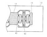
以下、本発明をその実施の形態を示す図面に基づいて説明する。図1は本実施の形態の照明装置100の構成の一例を示す外観斜視図であり、図2は本実施の形態の照明装置100の構成の一例を示す要部断面図であり、図3は固定板10の一例を示す要部平面図である。図1乃至図3に示すように、照明装置100は、矩形状であって板状の固定板10、固定板10の周縁に設けられた枠部20、固定板10と対向し、枠部20に嵌合する透過板30、固定板10に直接実装された半導体発光素子としてのLEDチップ40などを備える。 Hereinafter, the present invention will be described with reference to the drawings illustrating embodiments thereof. FIG. 1 is an external perspective view showing an example of the configuration of the
LEDチップ40からの光が透過板30を透過して外部へ放出される。透過板30は、透明でもよく、また半透明でもよく、光を拡散させる拡散性を有してもよい。透過板30は照明装置100の発光面となる。また、照明装置100の厚みは、枠部20の厚み(高さ寸法)とすることができる。 Light from the
固定板10は、高熱伝導性の合成樹脂製である。固定板10は、高熱伝導性として、例えば、2W/m・K以上10W/m・K以下程度の熱伝導率を有し、かつ絶縁性を有する。高熱伝導性の合成樹脂として、例えば、ポリフェニレンサルファイド樹脂などの熱可塑性樹脂を用いることができる。固定板10の厚みは、例えば、2〜3mm程度とすることができるが、厚み寸法はこれに限定されるものではなく、固定板10の形状又は大きさに応じて、5mm、10mm程度とすることもできる。 The
図3に示すように、固定板10の一面には、配線パターン15を形成してある。配線パターン15は、例えば、スクリーン印刷などの手法を用いて固定板10に形成することができる。なお、配線パターン15の形成方法は適宜の方法を用いることができる。 As shown in FIG. 3, a
固定板10の配線パターン15が形成された一面には、複数のLEDチップ40を実装してある。また、固定板10の他の面には放熱部11を設けている。なお、放熱部11は、LEDチップ40の実装領域に応じて、例えば、固定板10の全面に設けてもよく、あるいは固定板10の他面の一部に設けてもよい。 A plurality of
放熱部11は、突状の放熱フィン111と、放熱フィン111の間に形成された溝112とを有する。溝112の形状は、固定板10の平面視において、例えば、細長い矩形状であって、列状に複数設けられ、固定板10の断面視において、例えば、略U字状をなす。なお、溝112の形状は、これに限定されるものではなく、例えば、格子状に形成してもよく、また断面形状は、半円状、三角形状などであってもよい。 The
枠部20は、固定板10の周りに周設してある。なお、枠部20は、固定板10と一体成形してもよく、あるいは固定板10とは別個の部材とすることもできる。枠部20は、固定板10の一面に対して傾斜した傾斜面を有する側部22、及び透過板30の周縁を嵌合する嵌合部21などを有する。 The
固定板10の一面(LEDチップ40の実装面)及び側部22の傾斜面には、例えば、高反射白色レジストなどの高反射部材を塗布又は貼付してある。これにより、LEDチップ40からの光を効率よく透過板30の方へ反射させることができる。また、従来のような反射板をねじ等で固定する必要がない。 On one surface of the fixing plate 10 (the mounting surface of the LED chip 40) and the inclined surface of the
図4は固定板10に実装されたLEDチップ40の構成の一例を示す断面図である。図4に示すように、LEDチップ40は、基板41、n型半導体層42、p型半導体層43、電極44、絶縁層45などを有する。なお、図4では簡便のため放熱部11は省略している。また、図4においては、簡便のため、n型半導体層42及びp型半導体層43と電極44とを繋ぐ配線は省略している。 FIG. 4 is a cross-sectional view showing an example of the configuration of the
LEDチップ40は、例えば、平面視が矩形状の基板41の一面411にn型半導体層42、活性層(不図示)及びp型半導体層43を積層した半導体発光層(LED構造)を形成してある。また、基板41の一面411には、基板41の両側に、固定板10に形成された配線パターン15に半田付け等で電気的に接続するための一対の電極44を形成してある。また、LEDチップ40の一面411側は、電極44の表面を除いて絶縁層45で被覆してある。半導体発光層から放出された光は、主に基板41の他面412側から外部へ放出される。 The
固定板10の一面には、透光性であってLEDチップ40を封止する封止部60を設けてある。封止部60は、蛍光体を含有してもよく、含有していなくてもよい。蛍光体を含有する場合、例えば、黄色蛍光体を用いることができる。黄色蛍光体は、例えば、450nm〜480nmの範囲の波長の光を吸収して540nm〜600nmの範囲にピークを有する黄色(黄緑色、及び黄色に近い橙色も含む)の光を発光する。これにより、演色性の優れた白色光源を実現することができる。なお、蛍光体は、黄色蛍光体に限定されるものではなく、他の蛍光体でもよく、所要の発光色を実現するために適宜異なる蛍光体を用いることができる。蛍光体の材質を変えることにより所望の発光色を得ることができる。また、蛍光体を含有した封止部60を設ける代わりに、基板41の他面412上に蛍光体を含有したシートを設けることで封止部としてもよい。また、封止部60の表面に蛍光体を含有したシートを設けて、当該シートを含めて封止部60とすることもできる。 On one surface of the fixed
LEDチップ40は、電極44と配線パターン15とは、半田70により電気的に接続してある。LEDチップ40の厚み(高さ)は、例えば、約200μmであり、封止部60の高さは、例えば、1mm程度である。 In the
上述のように、本実施の形態の照明装置100では、固定板10は、一面に配線パターン15を形成してあり、他面に凹状の溝112を有する放熱部11を形成してある。固定板10の一面にLEDチップ40を設けてあり、LEDチップ40は、基板41と、基板41の一面411に形成された半導体発光層(42、43)と、基板41の一面411に形成され、半導体発光層に接続された電極44とを備える。電極44を配線パターン15に接続してあり、基板41の他面412から光を取り出す。すなわち、一面に配線パターン15を形成し、他面に放熱部11を有する固定板10の当該一面にLEDチップ40を直接実装してある。これにより、LEDチップ40を実装するための実装基板が不要となり、また、実装基板を照明装置に固定するねじ等、及び実装基板に設けたコネクタなどの部品が不要となるので、これらの部材によって占められた寸法(例えば、5mm〜10mm程度)だけ薄くすることができ、照明装置の薄型化を図ることができる。また、実装基板の取付工程が不要となり、実装基板及びコネクタなどの部品コスト及び製造コストを低減することができる。 As described above, in the
また、本実施の形態の照明装置100では、LEDチップ40の電極44を半田70で直接配線パターン15に接続してあり、従来のLEDチップのようなボンディングワイヤを用いていないので、当該ボンディングワイヤと封止樹脂との熱膨張率の差により、周囲温度が変化した場合に、ワイヤの断線又はワイヤの接点箇所の剥がれなどの異常が発生することもない。 Further, in the
また、本実施の形態の照明装置100では、固定板10の一面に直接LEDチップ40を実装するので、LEDチップ40を実装した実装基板の照明装置への取付、実装基板への配線の接続、実装基板を複数設ける場合には、実装基板同士の接続などの従来の照明装置において必要であった品質保証上のチェック項目及び故障の要因となる箇所がなくなり、品質向上を図ることができる。 Further, in the
また、本実施の形態の照明装置100では、実装基板が不要であるので、従来であれば実装基板の形状などの制約によりLEDチップ40の位置が制約されていたという問題もなく、固定板10の任意の箇所に配線パターンを形成し、LEDチップ40の位置を比較的自由に設定することが可能となる。 Moreover, since the mounting board is unnecessary in the
また、固定板10の材料として、高熱伝導性樹脂(高放熱性樹脂)を用いることにより、照明装置本体を絶縁性にすることができ、絶縁性能を比較的容易に確保することができる。なお、固定板10は、アルミニウムなどの金属製であってもよい。この場合には、LEDチップ40を実装する面に必要に応じて絶縁膜を塗布すればよい。 Further, by using a high thermal conductive resin (high heat dissipation resin) as the material of the fixing
また、本実施の形態の照明装置100では、固定板10の一面に、透光性であってLEDチップ40を封止する封止部60を設けてある。固定板10の一面に封止部60を形成してあるので、LEDチップ40及び封止部60などを含む発光部の寸法(高さ寸法)を小さくすることができ、照明装置の超薄型化を図ることができる。 Moreover, in the illuminating
また、固定板10は、高熱伝導性を有するため、固定板10の一面に実装したLEDチップ40の熱を、固定板10の他面の放熱部11を介して効率良く外部へ放熱させることができる。 Further, since the fixing
また、本実施の形態の照明装置100では、固定板10の周縁に設けられた枠部20と、枠部20に嵌合し、LEDチップ40からの光を透過する透過板30とを備える。これにより、固定板10と透過板30とを対設させ、周りを枠部20で囲んだ薄型の照明装置を実現することができる。 In addition, the
照明装置の形状は、図1に例示したものに限定されるものではない。本実施の形態は、天井又は壁等の取付孔に取り付ける埋込形の照明装置、ダウンライト、壁面などに取り付けるものなど種々のタイプの照明装置に適用することができる。 The shape of the lighting device is not limited to that illustrated in FIG. The present embodiment can be applied to various types of illumination devices such as an embedded illumination device attached to an attachment hole such as a ceiling or a wall, a downlight, a device attached to a wall surface, and the like.
10 固定板
11 放熱部
15 配線パターン
20 枠部
30 透過板
40 LEDチップ
41 基板
42 n型半導体層
43 p型半導体層
44 電極
60 封止部DESCRIPTION OF
Claims (3)
Translated fromJapanese前記固定板は、
一面に配線パターンを形成してあり、
他面に溝を有する放熱部を形成してあり、
前記一面に前記半導体発光素子を設けてあり、
該半導体発光素子は、
基板と、
該基板の一面に形成された半導体発光層と、
前記基板の一面に形成され、前記半導体発光層に接続された電極と
を備え、
該電極を前記配線パターンに接続してあり、
前記基板の他面から光を取り出すようにしてあり、
前記固定板の周縁に設けられ、該固定板と一体成形された枠部と、
該枠部に嵌合し、前記半導体発光素子からの光を透過する透過板と
をさらに備えることを特徴とする照明装置。A lighting device comprising a fixed plate to which a semiconductor light emitting element is fixed,
The fixing plate is
A wiring pattern is formed on one side,
A heat dissipation part having a groove on the other surface is formed,
The semiconductor light emitting element is provided on the one surface,
The semiconductor light emitting device is
A substrate,
A semiconductor light emitting layer formed on one surface of the substrate;
An electrode formed on one surface of the substrate and connected to the semiconductor light emitting layer,
The electrode is connected to the wiring pattern;
Ri Citea so light is extracted from the other surface of thesubstrate,
A frame portion provided at a peripheral edge of the fixing plate and integrally formed with the fixing plate;
A transmission plate that fits into the frame and transmits light from the semiconductor light emitting element;
Further comprising an illumination device according to claim Rukotoa.
高熱伝導性の合成樹脂製であることを特徴とする請求項1又は請求項2に記載の照明装置。The fixing plate is
The lighting device according to claim 1 or 2, wherein the lighting device is made of a highly heat-conductive synthetic resin.
Priority Applications (1)
| Application Number | Priority Date | Filing Date | Title |
|---|---|---|---|
| JP2012266580AJP6085459B2 (en) | 2012-12-05 | 2012-12-05 | Lighting device |
Applications Claiming Priority (1)
| Application Number | Priority Date | Filing Date | Title |
|---|---|---|---|
| JP2012266580AJP6085459B2 (en) | 2012-12-05 | 2012-12-05 | Lighting device |
Publications (2)
| Publication Number | Publication Date |
|---|---|
| JP2014112495A JP2014112495A (en) | 2014-06-19 |
| JP6085459B2true JP6085459B2 (en) | 2017-02-22 |
Family
ID=51169499
Family Applications (1)
| Application Number | Title | Priority Date | Filing Date |
|---|---|---|---|
| JP2012266580AExpired - Fee RelatedJP6085459B2 (en) | 2012-12-05 | 2012-12-05 | Lighting device |
Country Status (1)
| Country | Link |
|---|---|
| JP (1) | JP6085459B2 (en) |
Families Citing this family (2)
| Publication number | Priority date | Publication date | Assignee | Title |
|---|---|---|---|---|
| CN107636390A (en)* | 2015-03-20 | 2018-01-26 | 沙特基础工业全球技术公司 | Plastic heat sinks for lighting equipment |
| JP7481901B2 (en)* | 2020-05-21 | 2024-05-13 | 株式会社ジャパンディスプレイ | Display device |
Family Cites Families (3)
| Publication number | Priority date | Publication date | Assignee | Title |
|---|---|---|---|---|
| TWI420686B (en)* | 2004-12-10 | 2013-12-21 | 松下電器產業股份有限公司 | Semiconductor light emitting device, light emitting module and lighting device |
| JP5584852B2 (en)* | 2010-07-16 | 2014-09-10 | 株式会社オプトデザイン | Surface illumination light source device |
| JP2012033558A (en)* | 2010-07-28 | 2012-02-16 | Kantatsu Co Ltd | Led unit |
- 2012
- 2012-12-05JPJP2012266580Apatent/JP6085459B2/ennot_activeExpired - Fee Related
Also Published As
| Publication number | Publication date |
|---|---|
| JP2014112495A (en) | 2014-06-19 |
Similar Documents
| Publication | Publication Date | Title |
|---|---|---|
| CN100407453C (en) | Surface-mounted LED and light-emitting device using the same | |
| JP5658394B2 (en) | Lamp and lighting device | |
| JP5029822B2 (en) | Light source and lighting device | |
| JP4802304B2 (en) | Semiconductor light emitting module and manufacturing method thereof | |
| US8783911B2 (en) | LED packaging structure having improved thermal dissipation and mechanical strength | |
| US8616732B2 (en) | Light-emitting device and illumination device | |
| JP4808550B2 (en) | Light emitting diode light source device, lighting device, display device, and traffic signal device | |
| JP2006295085A (en) | Light-emitting diode light source unit | |
| CN103470983A (en) | Light-emitting element lamp and lighting equipment | |
| JP5757214B2 (en) | LED lighting device | |
| JP4683013B2 (en) | Light emitting device | |
| WO2011024861A1 (en) | Light-emitting device and illuminating device | |
| JP4674487B2 (en) | Surface mount light emitting device | |
| US8791482B2 (en) | Light emitting device package | |
| KR101940987B1 (en) | Printed circuit board with heatsink for led lighting apparatus | |
| US10222048B2 (en) | Light emitting device and method for manufacturing a light emitting device | |
| JP6085459B2 (en) | Lighting device | |
| WO2012057276A1 (en) | Light-emitting module, and lighting equipment | |
| JP5845053B2 (en) | LED lamp | |
| JP2009021384A (en) | Electronic component and light emitting device | |
| TWI519735B (en) | Led lamp with heat dissipating structures | |
| KR20130003414A (en) | Led lamp | |
| JP6979628B2 (en) | Mounting structure of light source board | |
| CN203718434U (en) | Lamp | |
| TWI523271B (en) | Plug-in light-emitting unit and light-emitting device |
Legal Events
| Date | Code | Title | Description |
|---|---|---|---|
| A621 | Written request for application examination | Free format text:JAPANESE INTERMEDIATE CODE: A621 Effective date:20150915 | |
| RD02 | Notification of acceptance of power of attorney | Free format text:JAPANESE INTERMEDIATE CODE: A7422 Effective date:20150915 | |
| A977 | Report on retrieval | Free format text:JAPANESE INTERMEDIATE CODE: A971007 Effective date:20160624 | |
| A131 | Notification of reasons for refusal | Free format text:JAPANESE INTERMEDIATE CODE: A131 Effective date:20160705 | |
| A521 | Request for written amendment filed | Free format text:JAPANESE INTERMEDIATE CODE: A523 Effective date:20160819 | |
| TRDD | Decision of grant or rejection written | ||
| A01 | Written decision to grant a patent or to grant a registration (utility model) | Free format text:JAPANESE INTERMEDIATE CODE: A01 Effective date:20170117 | |
| A61 | First payment of annual fees (during grant procedure) | Free format text:JAPANESE INTERMEDIATE CODE: A61 Effective date:20170130 | |
| R150 | Certificate of patent or registration of utility model | Ref document number:6085459 Country of ref document:JP Free format text:JAPANESE INTERMEDIATE CODE: R150 | |
| R250 | Receipt of annual fees | Free format text:JAPANESE INTERMEDIATE CODE: R250 | |
| LAPS | Cancellation because of no payment of annual fees |