JP6083089B2 - Semiconductor device, display device and electronic apparatus - Google Patents
Semiconductor device, display device and electronic apparatusDownload PDFInfo
- Publication number
- JP6083089B2 JP6083089B2JP2013066219AJP2013066219AJP6083089B2JP 6083089 B2JP6083089 B2JP 6083089B2JP 2013066219 AJP2013066219 AJP 2013066219AJP 2013066219 AJP2013066219 AJP 2013066219AJP 6083089 B2JP6083089 B2JP 6083089B2
- Authority
- JP
- Japan
- Prior art keywords
- film
- oxide semiconductor
- electrode
- conductive film
- gate electrode
- Prior art date
- Legal status (The legal status is an assumption and is not a legal conclusion. Google has not performed a legal analysis and makes no representation as to the accuracy of the status listed.)
- Active
Links
Images


Classifications
- H—ELECTRICITY
- H10—SEMICONDUCTOR DEVICES; ELECTRIC SOLID-STATE DEVICES NOT OTHERWISE PROVIDED FOR
- H10D—INORGANIC ELECTRIC SEMICONDUCTOR DEVICES
- H10D30/00—Field-effect transistors [FET]
- H10D30/60—Insulated-gate field-effect transistors [IGFET]
- H10D30/67—Thin-film transistors [TFT]
- H10D30/674—Thin-film transistors [TFT] characterised by the active materials
- H10D30/6755—Oxide semiconductors, e.g. zinc oxide, copper aluminium oxide or cadmium stannate
- G—PHYSICS
- G02—OPTICS
- G02F—OPTICAL DEVICES OR ARRANGEMENTS FOR THE CONTROL OF LIGHT BY MODIFICATION OF THE OPTICAL PROPERTIES OF THE MEDIA OF THE ELEMENTS INVOLVED THEREIN; NON-LINEAR OPTICS; FREQUENCY-CHANGING OF LIGHT; OPTICAL LOGIC ELEMENTS; OPTICAL ANALOGUE/DIGITAL CONVERTERS
- G02F1/00—Devices or arrangements for the control of the intensity, colour, phase, polarisation or direction of light arriving from an independent light source, e.g. switching, gating or modulating; Non-linear optics
- G02F1/01—Devices or arrangements for the control of the intensity, colour, phase, polarisation or direction of light arriving from an independent light source, e.g. switching, gating or modulating; Non-linear optics for the control of the intensity, phase, polarisation or colour
- G02F1/13—Devices or arrangements for the control of the intensity, colour, phase, polarisation or direction of light arriving from an independent light source, e.g. switching, gating or modulating; Non-linear optics for the control of the intensity, phase, polarisation or colour based on liquid crystals, e.g. single liquid crystal display cells
- G02F1/133—Constructional arrangements; Operation of liquid crystal cells; Circuit arrangements
- G02F1/136—Liquid crystal cells structurally associated with a semi-conducting layer or substrate, e.g. cells forming part of an integrated circuit
- G02F1/1362—Active matrix addressed cells
- G02F1/136213—Storage capacitors associated with the pixel electrode
- H—ELECTRICITY
- H10—SEMICONDUCTOR DEVICES; ELECTRIC SOLID-STATE DEVICES NOT OTHERWISE PROVIDED FOR
- H10D—INORGANIC ELECTRIC SEMICONDUCTOR DEVICES
- H10D86/00—Integrated devices formed in or on insulating or conducting substrates, e.g. formed in silicon-on-insulator [SOI] substrates or on stainless steel or glass substrates
- H10D86/40—Integrated devices formed in or on insulating or conducting substrates, e.g. formed in silicon-on-insulator [SOI] substrates or on stainless steel or glass substrates characterised by multiple TFTs
- H10D86/421—Integrated devices formed in or on insulating or conducting substrates, e.g. formed in silicon-on-insulator [SOI] substrates or on stainless steel or glass substrates characterised by multiple TFTs having a particular composition, shape or crystalline structure of the active layer
- H10D86/423—Integrated devices formed in or on insulating or conducting substrates, e.g. formed in silicon-on-insulator [SOI] substrates or on stainless steel or glass substrates characterised by multiple TFTs having a particular composition, shape or crystalline structure of the active layer comprising semiconductor materials not belonging to the Group IV, e.g. InGaZnO
- H—ELECTRICITY
- H10—SEMICONDUCTOR DEVICES; ELECTRIC SOLID-STATE DEVICES NOT OTHERWISE PROVIDED FOR
- H10D—INORGANIC ELECTRIC SEMICONDUCTOR DEVICES
- H10D86/00—Integrated devices formed in or on insulating or conducting substrates, e.g. formed in silicon-on-insulator [SOI] substrates or on stainless steel or glass substrates
- H10D86/40—Integrated devices formed in or on insulating or conducting substrates, e.g. formed in silicon-on-insulator [SOI] substrates or on stainless steel or glass substrates characterised by multiple TFTs
- H10D86/481—Integrated devices formed in or on insulating or conducting substrates, e.g. formed in silicon-on-insulator [SOI] substrates or on stainless steel or glass substrates characterised by multiple TFTs integrated with passive devices, e.g. auxiliary capacitors
- H—ELECTRICITY
- H10—SEMICONDUCTOR DEVICES; ELECTRIC SOLID-STATE DEVICES NOT OTHERWISE PROVIDED FOR
- H10D—INORGANIC ELECTRIC SEMICONDUCTOR DEVICES
- H10D86/00—Integrated devices formed in or on insulating or conducting substrates, e.g. formed in silicon-on-insulator [SOI] substrates or on stainless steel or glass substrates
- H10D86/40—Integrated devices formed in or on insulating or conducting substrates, e.g. formed in silicon-on-insulator [SOI] substrates or on stainless steel or glass substrates characterised by multiple TFTs
- H10D86/60—Integrated devices formed in or on insulating or conducting substrates, e.g. formed in silicon-on-insulator [SOI] substrates or on stainless steel or glass substrates characterised by multiple TFTs wherein the TFTs are in active matrices
- H—ELECTRICITY
- H10—SEMICONDUCTOR DEVICES; ELECTRIC SOLID-STATE DEVICES NOT OTHERWISE PROVIDED FOR
- H10D—INORGANIC ELECTRIC SEMICONDUCTOR DEVICES
- H10D86/00—Integrated devices formed in or on insulating or conducting substrates, e.g. formed in silicon-on-insulator [SOI] substrates or on stainless steel or glass substrates
- H10D86/80—Integrated devices formed in or on insulating or conducting substrates, e.g. formed in silicon-on-insulator [SOI] substrates or on stainless steel or glass substrates characterised by multiple passive components, e.g. resistors, capacitors or inductors
- H—ELECTRICITY
- H10—SEMICONDUCTOR DEVICES; ELECTRIC SOLID-STATE DEVICES NOT OTHERWISE PROVIDED FOR
- H10K—ORGANIC ELECTRIC SOLID-STATE DEVICES
- H10K59/00—Integrated devices, or assemblies of multiple devices, comprising at least one organic light-emitting element covered by group H10K50/00
- H10K59/10—OLED displays
- H10K59/12—Active-matrix OLED [AMOLED] displays
- H10K59/121—Active-matrix OLED [AMOLED] displays characterised by the geometry or disposition of pixel elements
- H10K59/1213—Active-matrix OLED [AMOLED] displays characterised by the geometry or disposition of pixel elements the pixel elements being TFTs
- H—ELECTRICITY
- H10—SEMICONDUCTOR DEVICES; ELECTRIC SOLID-STATE DEVICES NOT OTHERWISE PROVIDED FOR
- H10K—ORGANIC ELECTRIC SOLID-STATE DEVICES
- H10K59/00—Integrated devices, or assemblies of multiple devices, comprising at least one organic light-emitting element covered by group H10K50/00
- H10K59/10—OLED displays
- H10K59/12—Active-matrix OLED [AMOLED] displays
- H10K59/121—Active-matrix OLED [AMOLED] displays characterised by the geometry or disposition of pixel elements
- H10K59/1216—Active-matrix OLED [AMOLED] displays characterised by the geometry or disposition of pixel elements the pixel elements being capacitors
- H—ELECTRICITY
- H10—SEMICONDUCTOR DEVICES; ELECTRIC SOLID-STATE DEVICES NOT OTHERWISE PROVIDED FOR
- H10K—ORGANIC ELECTRIC SOLID-STATE DEVICES
- H10K59/00—Integrated devices, or assemblies of multiple devices, comprising at least one organic light-emitting element covered by group H10K50/00
- H10K59/10—OLED displays
- H10K59/12—Active-matrix OLED [AMOLED] displays
Landscapes
- Physics & Mathematics (AREA)
- Engineering & Computer Science (AREA)
- Microelectronics & Electronic Packaging (AREA)
- Geometry (AREA)
- Nonlinear Science (AREA)
- Chemical & Material Sciences (AREA)
- Mathematical Physics (AREA)
- Crystallography & Structural Chemistry (AREA)
- Power Engineering (AREA)
- General Physics & Mathematics (AREA)
- Optics & Photonics (AREA)
- Thin Film Transistor (AREA)
- Electroluminescent Light Sources (AREA)
- Devices For Indicating Variable Information By Combining Individual Elements (AREA)
- Semiconductor Integrated Circuits (AREA)
Description
Translated fromJapanese本技術は、酸化物半導体膜を有する半導体装置、表示装置および電子機器に関する。 The present technology relates to a semiconductor device, a display device, and an electronic device having an oxide semiconductor film.
亜鉛(Zn)やインジウム(In)を含む酸化物は、半導体デバイスの活性層として優れた性質を示し、近年、TFT,発光デバイス,透明導電膜などへの応用を目指して開発が進められている。特に、Zn,In,Gaの複合酸化物を用いたTFTは、液晶ディスプレイなどに一般的に使用される非晶質シリコン(a−Si:H)を用いたTFTと比較してその電子移動度が大きく、優れた電気特性を示すことがわかっている。 Oxides containing zinc (Zn) and indium (In) exhibit excellent properties as active layers in semiconductor devices, and are currently being developed for applications in TFTs, light-emitting devices, transparent conductive films, etc. . In particular, a TFT using a complex oxide of Zn, In, and Ga has an electron mobility compared to a TFT using amorphous silicon (a-Si: H) generally used for a liquid crystal display or the like. Is known to exhibit large electrical properties.
このような酸化物半導体を用いたTFT(Thin Film Transistor)では、ボトムゲート型およびトップゲート型のTFTがこれまでに報告されている。ボトムゲート型の構造は、ゲート電極上にゲート絶縁膜を間にして酸化物半導体の薄膜層を設けたものである。この構造は、現在事業化されている、非晶質シリコンをチャネルとして用いたTFT構造と類似している。このため、既存の非晶質シリコンによるTFTの製造プロセスを転用し易く、酸化物半導体を利用したTFTにおいても、ボトムゲート型の構造が多く用いられている。 As TFTs (Thin Film Transistors) using such an oxide semiconductor, bottom gate type and top gate type TFTs have been reported so far. In the bottom gate structure, an oxide semiconductor thin film layer is provided over a gate electrode with a gate insulating film therebetween. This structure is similar to a TFT structure using amorphous silicon as a channel, which is currently commercialized. For this reason, it is easy to divert the manufacturing process of the existing amorphous silicon TFT, and the bottom gate type structure is often used also in the TFT using the oxide semiconductor.
上記のようにして、酸化物半導体材料はTFTのチャネル膜として用いられる一方、その導電性を高めて容量素子の電極などに用いる方法も検討されている(例えば特許文献1)。酸化物半導体材料では、酸素欠陥によりキャリアが生成する。即ち、酸化物半導体材料に還元処理を施すことで、その導電性を向上させることが可能となる。還元処理としては、例えば、アルゴン処理、窒素(N2)雰囲気下でのアニールまたは水素処理等が挙げられる(例えば、特許文献2〜4)。水素処理とは、例えば水素プラズマ照射である。As described above, an oxide semiconductor material is used as a channel film of a TFT. On the other hand, a method of increasing the conductivity of the oxide semiconductor material and using it for an electrode of a capacitor element has been studied (for example, Patent Document 1). In an oxide semiconductor material, carriers are generated due to oxygen defects. That is, by performing reduction treatment on the oxide semiconductor material, the conductivity can be improved. Examples of the reduction treatment include argon treatment, annealing in a nitrogen (N2 ) atmosphere, or hydrogen treatment (for example,
しかしながらデバイスの製造工程では、酸化物半導体材料に還元処理を行った後も、酸化処理等の様々な処理が施されるため、酸化物半導体材料の導電性を安定して維持することは困難である。 However, in the device manufacturing process, it is difficult to stably maintain the conductivity of the oxide semiconductor material because various treatments such as oxidation treatment are performed after the reduction treatment of the oxide semiconductor material. is there.
本技術はかかる問題点に鑑みてなされたもので、その目的は、安定した導電性の酸化物半導体膜を有する半導体装置、表示装置および電子機器を提供することにある。 The present technology has been made in view of such problems, and an object of the present technology is to provide a semiconductor device, a display device, and an electronic device having a stable conductive oxide semiconductor film.
本技術による半導体装置は、トランジスタと共に、酸化物半導体膜と、酸化物半導体膜に電気的に接続された第1導電膜と、第1導電膜と酸化物半導体膜との間の第1絶縁膜とを備えたものである。 A semiconductor device according to the present technology includes a transistor, an oxide semiconductor film, a first conductive film electrically connected to the oxide semiconductor film, and a first insulating film between the first conductive film and the oxide semiconductor film It is equipped with.
本技術による半導体装置は、ゲート電極およびゲート電極に対向するチャネル膜を有するトランジスタと、酸化物半導体膜および酸化物半導体膜に電気的に接続された第1導電膜が一方の電極、酸化物半導体膜を間にして第1導電膜に対向する第2導電膜が他方の電極を構成する容量素子と、第1導電膜と前記酸化物半導体膜との間の第1絶縁膜と、第2導電膜と酸化物半導体膜との間の第2絶縁膜とを備え、ゲート電極と同層に第1導電膜、チャネル膜と同層に酸化物半導体膜がそれぞれ配置され、第1絶縁膜はゲート電極とチャネル膜との間に延在しているものである。In the semiconductor device according to the present technology, a transistorhaving a gate electrode and a channel film facing the gate electrode,an oxide semiconductor film,and a first conductive film electrically connected tothe oxide semiconductor filmare provided on one electrode, the oxide semiconductor A capacitor element in which the second conductive film facing the first conductive film with the film interposed therebetween constitutes the other electrode, a first insulating film between the first conductive film and the oxide semiconductor film, and asecond conductive filmA second insulating film between the film and the oxide semiconductor film, the first conductive film is disposed in the same layer as the gate electrode, and the oxide semiconductor film is disposed in the same layer as the channel film. It extends between the electrode and the channel film .
本技術による第1の表示装置は、上記本技術の半導体装置を備えたものである。本技術による第2の表示装置は、酸化物半導体膜および酸化物半導体膜に電気的に接続された第1導電膜により構成された第1電極と、第1電極に対向する第2電極と、第1電極と第2電極との間の表示層と、ゲート電極およびゲート電極に対向するチャネル膜を有し、表示層を駆動するトランジスタと、第1導電膜と酸化物半導体膜との間の第1絶縁膜とを備え、ゲート電極と同層に第1導電膜、チャネル膜と同層に酸化物半導体膜がそれぞれ配置され、第1絶縁膜はゲート電極とチャネル膜との間に延在しているものである。Afirst display device according to the present technology includes the semiconductor device according to the present technology. Asecond display device according tothe present technology includes anoxide semiconductor film, a first electrode formed of a first conductive film electrically connected to the oxide semiconductor film, a second electrode facing the first electrode, A display layer between the first electrode and the second electrode; a gate electrode; a channel film facing the gate electrode; a transistor for driving the display layer; and the first conductive film and the oxide semiconductor film And a first conductive film in the same layer as the gate electrode, an oxide semiconductor film in the same layer as the channel film, and the first insulating film extending between the gate electrode and the channel film. It is what you are doing.
本技術による第1の電子機器は、上記本技術の第1の表示装置を備えたものである。本技術による第2の電子機器は、上記本技術の第2の表示装置を備えたものである。Afirst electronic device according to the present technology includesthe first display device according tothe present technology.A second electronic device according to the present technology includes the second display device according to the present technology.
本技術の半導体装置、表示装置および電子機器では、第1導電膜により酸化物半導体膜内のキャリア生成量を制御するようにしたので、酸化物半導体膜の導電性を安定して維持することができる。 In the semiconductor device, the display device, and the electronic device of the present technology, the carrier generation amount in the oxide semiconductor film is controlled by the first conductive film, so that the conductivity of the oxide semiconductor film can be stably maintained. it can.
以下、本技術の実施の形態について、図面を参照して詳細に説明する。なお、説明は以下の順序で行う。
1.第1の実施の形態(酸化物半導体膜および第1導電膜が容量素子の一方の電極を構成する例)
2.第2の実施の形態(酸化物半導体膜および第1導電膜が表示層を間にした一対の電極の一方を構成する例)Hereinafter, embodiments of the present technology will be described in detail with reference to the drawings. The description will be given in the following order.
1. First Embodiment (Example in which an oxide semiconductor film and a first conductive film constitute one electrode of a capacitor)
2. Second Embodiment (Example in which an oxide semiconductor film and a first conductive film constitute one of a pair of electrodes with a display layer in between)
〔第1の実施の形態〕
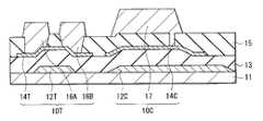
図1は第1の実施の形態に係る半導体装置(半導体装置10)の断面構成を表している。半導体装置10は、基板11上の互いに隣り合う位置にトランジスタ10Tおよび容量素子10Cを有するものであり、例えば図2に示したような表示装置1に適用される。[First Embodiment]
FIG. 1 shows a cross-sectional configuration of the semiconductor device (semiconductor device 10) according to the first embodiment. The
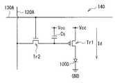
表示装置1は、例えば液晶層または有機EL(Electroluminescence)層等の表示層を含んでおり、この表示層が半導体装置10により画素100毎に駆動されるようになっている。表示領域110には、画素100がマトリクス状に二次元配置されると共に画素100を駆動するための画素駆動回路140が設けられている。画素駆動回路140において、列方向(Y方向)には複数の信号線120A(120A1,120A2,・・・,120Am,・・・)が配置され、行方向(X方向)には複数の走査線130A(130A1,・・・,130An,・・・)が配置されている。信号線120Aと走査線130Aとの交差点に、一の画素100が設けられている。信号線120Aはその両端が信号線駆動回路120に接続され、走査線130Aはその両端が走査線駆動回路130に接続されている。 The
信号線駆動回路120は、信号供給源(図示せず)から供給される輝度情報に応じた映像信号の信号電圧を、信号線120Aを介して選択された画素100に供給するものである。走査線駆動回路130は、入力されるクロックパルスに同期してスタートパルスを順にシフト(転送)するシフトレジスタなどによって構成されている。走査線駆動回路130は、各画素100への映像信号の書き込みに際し行単位でそれらを走査し、各走査線130Aに走査信号を順次供給するものである。信号線120Aには信号線駆動回路120からの信号電圧が、走査線130Aには走査線駆動回路130からの走査信号がそれぞれ供給されるようになっている。 The signal
図3に画素駆動回路140の一構成例を表す。上記半導体装置10は、例えばこの画素駆動回路140を構成するものである。画素駆動回路140は、駆動トランジスタTr1および書込トランジスタTr2と、その間のキャパシタ(容量素子10C)と、例えば有機EL素子等の表示素子100Dとを有するアクティブ型の駆動回路である。表示素子100Dは、駆動トランジスタTr1と直列に接続されている。駆動トランジスタTr1または書込トランジスタTr2のうちの少なくとも一方が半導体装置10のトランジスタ10Tにより構成されている。 FIG. 3 illustrates a configuration example of the
[半導体装置の要部構成]
次に、再び図1を参照して、半導体装置10の詳細な構成について説明する。[Configuration of main parts of semiconductor device]
Next, the detailed configuration of the
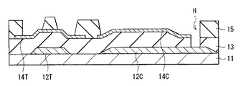
トランジスタ10Tは、基板11側からゲート電極12T、チャネル膜14Tおよびソース・ドレイン電極16A,16Bがこの順に配置されたボトムゲート型(逆スタガ型)の薄膜トランジスタである。ゲート電極12Tとチャネル膜14Tとの間には第1絶縁膜13が設けられており、チャネル膜14T上の一部は第2絶縁膜15により覆われている。 The
基板11は、ガラス基板やプラスチックフィルムなどにより構成されている。プラスチック材料としては、例えばPET(ポリエチレンテレフタレート)、PEN(ポリエチレンナフタレート)などが挙げられる。スパッタリング法等により、基板11を加熱することなく半導体層14を成膜することが可能であれば、基板11に安価なプラスチックフィルムを用いることも可能である。 The
ゲート電極12Tは、トランジスタ10Tにゲート電圧を印加し、このゲート電圧によりチャネル膜14T中のキャリア密度を制御する役割を有するものである。ゲート電極12Tは基板11上の選択的な領域に、例えば100nm〜500nmの厚みで設けられている。ゲート電極12Tは、例えば白金(Pt),チタン(Ti),ルテニウム(Ru),モリブデン(Mo),銅(Cu),タングステン(W),ニッケル(Ni),アルミニウム(Al)およびタンタル(Ta)等の金属単体または合金により構成されている。また、ゲート電極12Tをインジウム錫酸化物(ITO)、インジウム亜鉛酸化物(IZO)、酸化亜鉛(ZnO)等の透明導電性薄膜により構成してもよい。 The
第1絶縁膜13は、例えば、厚み100nm〜500nmの範囲で設けられており、ゲート絶縁膜として機能している。この第1絶縁膜13は、例えばシリコン酸化膜,シリコン窒化膜,シリコン酸窒化膜,ハフニウム酸化膜,アルミニウム酸化膜,アルミニウム窒化膜,タンタル酸化膜,ジルコニウム酸化膜,ハフニウム酸窒化膜,ハフニウムシリコン酸窒化膜,アルミニウム酸窒化膜,タンタル酸窒化膜およびジルコニウム酸窒化膜のうちの少なくとも1つを含む絶縁膜により形成される。第1絶縁膜13は単層構造としてもよく、または2種類以上の積層構造としてしてもよい。第1絶縁膜13を2種類以上の積層構造とした場合、チャネル膜14Tとの界面特性を改善したり、外気からチャネル膜14Tへの不純物の混入を抑制することが可能である。 For example, the first insulating
チャネル膜14Tは第1絶縁膜13上に島状に設けられており、ソース・ドレイン電極16Aとソース・ドレイン電極16Bとの間のゲート電極12Tに対向する位置にチャネル領域が形成される。チャネル膜14Tは、例えばインジウム(In),ガリウム(Ga),亜鉛(Zn),スズ(Sn),ジルコニウム(Zr),アルミニウム(Al)およびチタン(Ti)のうちの少なくとも1種の元素の酸化物を主成分として含む酸化物半導体により構成されている。具体的には、酸化亜鉛を主成分とする透明な酸化物半導体、例えば酸化インジウムガリウム亜鉛(IGZO),酸化亜鉛,アルミニウムドープ酸化亜鉛(AZO)またはガリウムドープ酸化亜鉛(GZO)等である。チャネル膜14Tの厚みは、製造工程でのアニールによる酸素供給効率を考慮すると、例えば5nm〜100nmであることが好ましい。チャネル膜14Tは非晶質状態であっても、結晶状態であってもよいが、結晶状態であればエッチング溶液に対する耐性が高くなり、デバイス構造形成への応用が容易となる。 The
第2絶縁膜15は、チャネル膜14Tのチャネル領域上に設けられ、ソース・ドレイン電極16A,16Bの形成時にチャネル膜14Tの損傷を防止するものである。第2絶縁膜15は、例えば、厚み50nm〜400nmのシリコン酸化膜,シリコン窒化膜または酸化アルミニウム膜等により構成されている。複数の種類の絶縁膜を積層させて第2絶縁膜15を構成するようにしてもよい。 The second insulating
ソース・ドレイン電極16A,16Bは、チャネル膜14T上に設けられ、チャネル膜14Tに電気的に接続されている。ソース・ドレイン電極16A,16Bは、例えばモリブデン,アルミニウム,銅,チタン,ITOまたはこれらの合金からなる金属膜の単層膜あるいは2種以上のこれらの金属膜よりなる積層膜である。例えば、モリブデン、アルミニウム、モリブデンの順に50nm、500nm、50nmの膜厚で積層した3層膜にすると、チャネル膜14Tの電気特性を安定して保持することができる。また、モリブデンの他、ITOあるいは酸化チタン等の酸素を含む金属膜がチャネル膜14Tに接触するように構成されていてもよい。酸化物半導体材料からなるチャネル膜14Tが酸素を引き抜き易い金属膜と接触すると、酸化物半導体の酸素が引き抜かれ、欠陥が形成されてしまう。よって、ソース・ドレイン電極16A,16Bのうち、チャネル膜14Tに接触する部分に酸素を含む金属膜を用いることによりトランジスタ10Tの電気特性を安定化させることができる。The source /
容量素子10Cは、基板11側から第1導電膜12C、半導体膜14C(酸化物半導体膜)および第2導電膜17をこの順に有するものである。第1絶縁膜13および第2絶縁膜15は、トランジスタ10Tおよび容量素子10Cに共通して設けられており、第1絶縁膜13は第1導電膜12Cと半導体膜14Cとの間、第2絶縁膜15は半導体膜14Cと第2導電膜17との間に延在している。本実施の形態では、半導体膜14Cに第1導電膜12Cを電気的に接続するための配線16Cが設けられている。即ち、半導体膜14Cと第1導電膜12Cとは互いに同電位となっている。詳細は後述するが、これにより第1導電膜12Cを介して半導体膜14C内のキャリア生成量を制御することが可能となり、半導体膜14Cの導電性を安定して維持することができる。The capacitive element 10C includes the first conductive film 12C, the
互いに電気的に接続された第1導電膜12Cおよび半導体膜14Cは容量素子10Cの下部電極(一方の電極)として機能するものである。例えば第1導電膜12Cはゲート電極12Tと、半導体膜14Cはチャネル膜14Tとそれぞれ同層に配置されている。第1導電膜12Cにはゲート電極12Tと同様の金属材料を、半導体膜14Cにはチャネル膜14Tと同様の酸化物半導体材料をそれぞれ用いることが可能である。第1導電膜12Cとゲート電極12T、半導体膜14Cとチャネル膜14T、それぞれの構成材料が互いに異なっていてもよい。 The first conductive film 12C and the
配線16Cは、半導体膜14Cに接して例えばその上面から端面を覆うと共に第1絶縁膜13を貫通して第1導電膜12Cに達している。第2導電膜17は、容量素子10Cの上部電極(他方の電極)であり、この第2導電膜17と半導体膜14Cとの間の第2絶縁膜15が容量絶縁膜としての役割を担っている。このように、容量素子10Cでは、トランジスタ10Tのゲート絶縁膜(第1絶縁膜13)とは別の絶縁膜(第2絶縁膜15)を容量絶縁膜として用いることができる。配線16Cおよび第2導電膜17には、ソース・ドレイン電極16A,16Bと同様の導電材料を用いることが可能であるが、それぞれの構成材料は異なっていてもよい。
The wiring 16C is in contact with the
このような半導体装置10は、例えば次のようにして製造することができる(図4A〜図4D)。 Such a
まず基板11の全面に例えばスパッタリング法やCVD(Chemical Vapor Deposition;化学気相成長)法を用いて金属薄膜を成膜する。次いで、この金属薄膜をフォトリソグラフィおよびエッチング法を用いてパターニングして、ゲート電極12Tおよび第1導電膜12Cを形成する(図4A)。 First, a metal thin film is formed on the entire surface of the
続いて、図4Bに示したように、ゲート電極12Tおよび第1導電膜12Cが設けられた基板11の全面に、例えばプラズマCVD法によりシリコン窒化膜およびシリコン酸化膜の積層膜よりなる第1絶縁膜13を形成する。このプラズマCVD法による第1絶縁膜13の形成は、例えば原料ガスとしてシラン,アンモニア(NH3)および窒素(N2)等のガスを用いてシリコン窒化膜を成膜し、例えば原料ガスとしてシランおよび一酸化二窒素等を含むガスを用いてシリコン酸化膜を成膜して行う。また、プラズマCVD法に代えて、スパッタリング法により、シリコン窒化膜,シリコン酸化膜,酸化アルミニウム膜または窒化アルミニウム膜よりなる第1絶縁膜13を形成してもよい。スパッタリング法では、ターゲットとしてシリコンを用い、スパッタリングの放電雰囲気中に酸素,水蒸気,窒素等を流して反応性プラズマスパッタリングとすることでシリコン酸化膜あるいはシリコン窒化膜等を形成する。Subsequently, as shown in FIG. 4B, a first insulation made of a laminated film of a silicon nitride film and a silicon oxide film is formed on the entire surface of the
第1絶縁膜13を形成した後、図4Cに示したように、例えばスパッタリング法により、第1絶縁膜13の上に例えば酸化物半導体材料を成膜し、これをパターニングすることによりチャネル膜14Tおよび半導体膜14Cを形成する。酸化物半導体材料として酸化インジウムガリウム亜鉛を用いる場合には、酸化インジウムガリウム亜鉛のセラミックをターゲットとしたDC(Direct Current;直流)スパッタリング法を用い、アルゴン(Ar)と酸素(O2)との混合ガスによりプラズマ放電を行う。なお、アルゴンおよび酸素ガスの導入は、プラズマ放電前に、真空容器内を真空度が1×10⁻⁴Pa以下になるまで排気した後に行う。After the formation of the first insulating
また、酸化物半導体材料として酸化亜鉛を用いる場合には、酸化亜鉛のセラミックをターゲットとしたRF(Radio Frequency;高周波)スパッタリング法を行う。または、亜鉛の金属ターゲットを用いてアルゴンおよび酸素を含むガス雰囲気中でDC電源を用いたスパッタリング法を行うようにしてもよい。 When zinc oxide is used as the oxide semiconductor material, an RF (Radio Frequency) sputtering method using a zinc oxide ceramic as a target is performed. Alternatively, a sputtering method using a DC power source may be performed in a gas atmosphere containing argon and oxygen using a zinc metal target.
このとき、チャネルとなるチャネル膜14Tおよび半導体膜14C中のキャリア濃度は、酸化物形成の際のアルゴンおよび酸素の流量比を変化させることで制御することが可能である。 At this time, the carrier concentration in the
更に、酸化物半導体材料に結晶性酸化物半導体を用いた場合には、酸化物半導体材料の成膜後に、例えばレーザ光の照射等による結晶化アニール処理を施すようにしてもよい。結晶性材料としては、例えば酸化亜鉛,インジウム,ガリウム,ジルコニウムおよびスズ等からなり、このうちのインジウムまたはスズの比率が他のものよりも高い酸化物半導体が挙げられる。 Further, in the case where a crystalline oxide semiconductor is used as the oxide semiconductor material, a crystallization annealing process such as laser light irradiation may be performed after the oxide semiconductor material is formed. Examples of the crystalline material include zinc oxide, indium, gallium, zirconium, tin, and the like, and an oxide semiconductor in which the ratio of indium or tin is higher than the others is given.
チャネル膜14Tおよび半導体膜14Cを設けた後、基板11の全面に例えばシリコン酸化膜またはシリコン窒化膜等の絶縁膜を成膜する。この絶縁膜をフォトリソグラフィおよびエッチングによりパターニングして、第2絶縁膜15を形成する(図4D)。この絶縁膜のパターニングでは、チャネル膜14Tとソース・ドレイン電極16A,16Bとの間の接続部分および半導体膜14Cと配線16Cとの間の接続部分には開口を設けておく。このパターニングと同時に、あるいは第2絶縁膜15を設けた後、第1絶縁膜13に第1導電膜12Cに達する接続孔Hを形成する。 After providing the
第1絶縁膜13に接続孔Hを設けた後、基板11の全面に例えばスパッタリング法により金属膜を成膜する。この金属膜をエッチング法によりパターニングして、ソース・ドレイン電極16A,16B、配線16Cおよび第2導電膜17を形成する。このように、ソース・ドレイン電極16A,16B、配線16Cおよび第2導電膜17を同一の金属膜から形成することにより、製造工程数を減らすことが可能となる。以上により、図1に示した半導体装置10(トランジスタ10Tおよび容量素子10C)が完成する。このようにして半導体装置10を含む画素駆動回路140を設けた後、表示層を形成して表示装置1を製造する。 After providing the connection hole H in the first insulating
この表示装置1では、各画素10に対して走査線駆動回路130から書込トランジスタTr2のゲート電極を介して走査信号が供給されると共に、信号線駆動回路120から画像信号が書込トランジスタTr2を介して容量素子10Cに保持される。すなわち、この容量素子10Cに保持された信号に応じて駆動トランジスタTr1がオンオフ制御され、これにより画素100に駆動電流が注入される。これらトランジスタTr1,Tr2(トランジスタ10T)では、ゲート電極12Tにしきい値電圧以上の電圧(ゲート電圧)が印加されると、ソース・ドレイン電極16Aとソース・ドレイン電極16Bとの間のチャネル膜14Tのチャネル領域中に電流(ドレイン電流)が生じ、上述のように駆動を行う。 In the
ここでは、容量素子10Cの半導体膜14Cに第1導電膜12Cが電気的に接続されているので、半導体膜14の導電性を安定して維持することができる。以下、これについて詳細に説明する。 Here, since the first conductive film 12C is electrically connected to the
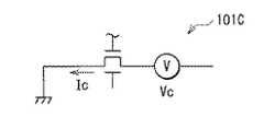
図5は比較例に係る半導体装置(半導体装置101)の断面構成を表したものである。この半導体装置101の容量素子101Cでは、半導体膜14Cが第1導電膜12Cに電気的に接続されておらず、半導体膜14Cおよび第1導電膜12Cが一対の電極として機能するようになっている。 FIG. 5 illustrates a cross-sectional configuration of a semiconductor device (semiconductor device 101) according to a comparative example. In the capacitive element 101C of the
図6Aは容量素子101Cの回路構成、図6Bは容量素子10Cの回路構成をそれぞれ模式的に表したものである。このような容量素子10C,101Cそれぞれを構成する半導体膜14Cに流れる電流および印加電圧のIV特性を図7A,図7Bに示す。図7Aは容量素子10C,101Cにコントロール電圧VCを印加したときに流れる電流ICの絶対値を表したものである。容量素子10Cには正のコントロール電圧VC、容量素子101Cには負のコントロール電圧VCを印加したときに電流ICが流れる。容量素子101Cでは半導体膜14Cが導電膜に接続されていないので、半導体膜14C内のキャリアが周辺電位による影響を受けやすい。従って、容量素子101Cに電流が流れ始める際のコントロール電圧VCは、ばらつきが大きく、0Vから離れている(図7A)。6A schematically illustrates the circuit configuration of the capacitive element 101C, and FIG. 6B schematically illustrates the circuit configuration of the capacitive element 10C. FIG. 7A and FIG. 7B show IV characteristics of current and applied voltage flowing in the
一方、容量素子10Cでは、半導体膜14Cに第1導電膜12Cが電気的に接続されているので、半導体膜14C内のキャリア生成量を制御し、キャリアを安定した状態で生成させることができる。これにより、半導体膜14Cおよび第1導電膜12Cがショットキー特性を示し、容量素子10Cには0V近傍から安定して電流ICが流れる(図7B)。このような半導体膜14Cの導電性は、半導体装置1の製造過程で様々な処理が施されることによっても維持される。On the other hand, in the capacitive element 10C, since the first conductive film 12C is electrically connected to the
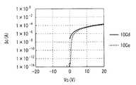
容量素子10Cの半導体膜14Cは、導体として用いることも可能である。図8A,図8Bに示したように、デプレッション特性を示す容量素子10Cdでは、負のコントロール電圧VCを印加した場合にも電流ICが流れる。即ち、常導性を示している。図8A,図8B中の実線は、デプレッション特性を示す容量素子10Cd、破線はエンハンスモードの容量素子10Ceをそれぞれ表している。The
また、容量素子10Cではトランジスタ10Tのゲート絶縁膜(第1絶縁膜13)とは別の絶縁膜(第2絶縁膜)を容量絶縁膜として用いることができるので、保持容量を向上させることが可能となる。 Further, in the capacitor 10C, an insulating film (second insulating film) different from the gate insulating film (first insulating film 13) of the
トランジスタ10Tにはチャネル保護膜(第2絶縁膜15)が設けられているので、平面視でゲート電極12Tとソース・ドレイン電極16A,16Bとが重なる領域(領域P)が大きくなる(図9)。これは、トランジスタ10Tを形成する際に、ゲート電極12Tに対するチャネル保護膜、ソース・ドレイン電極16A,16Bそれぞれのズレを考慮して余白を確保しておくためである。このような領域Pの増加により、トランジスタ10Tの寄生容量が増加する虞がある。 Since the channel protective film (second insulating film 15) is provided in the
容量素子101C(図5)ではトランジスタ10Tのゲート絶縁膜と同一の第1絶縁膜13が容量絶縁膜となるのに対し、容量素子10Cでは、保持容量の向上に適した第2絶縁膜15を選択することができる。例えば、第2絶縁膜15に用いる絶縁材料の誘電率を大きくすることで、容量素子10Cの保持容量を高めることができる。あるいは、第2絶縁膜15の膜厚を薄くするようにしてもよい。半導体装置10では、トランジスタ10Tの寄生容量が増加した場合にも装置全体での保持容量を大きくすることができ、これにより補正精度を向上させることが可能となる。 In the capacitive element 101C (FIG. 5), the first insulating
このように本実施の形態の半導体装置10では、半導体膜14Cに第1導電膜12Cを電気的に接続するようにしたので、半導体膜14Cの導電性を安定して維持することができる。 Thus, in the
また、トランジスタ10Tのゲート絶縁膜とは別に、容量絶縁膜(第2絶縁膜15)を選択することができるので、容量素子10Cの保持容量を向上させることが可能となる。 In addition, since the capacitor insulating film (second insulating film 15) can be selected separately from the gate insulating film of the
以下、他の実施の形態について説明するが、以降の説明において上記実施の形態と同一構成部分については同一符号を付してその説明は適宜省略する。 Hereinafter, other embodiments will be described. In the following description, the same components as those of the above-described embodiment will be denoted by the same reference numerals, and description thereof will be omitted as appropriate.
〔第2の実施の形態〕
図10は、本技術の第2の実施の形態に係る表示装置(表示装置2)の断面構成を表したものである。この表示装置2では、第1導電膜12Cおよび半導体膜14Cが有機EL素子の陽極(第1電極21)として用いられている。この点において表示装置2は、上記第1の実施の形態の半導体装置10と異なるものである。[Second Embodiment]
FIG. 10 illustrates a cross-sectional configuration of a display device (display device 2) according to the second embodiment of the present technology. In the
表示装置2は、例えばトップエミッション型の有機EL表示装置であり、トランジスタ10Tと隣り合う位置に有機EL素子20が配置されている。この有機EL素子20は、基板11側から第1電極21、隔壁22、有機層23および第2電極24をこの順に有している。 The
第1電極21は例えば画素100(図2)毎に設けられており、複数の第1電極21が基板11上に互いに離間して配置されている。図10は、一の画素100に対応する有機EL素子20を表している。本実施の形態では、半導体膜14Cに第1導電膜12Cを電気的に接続するようにしたので、半導体膜14Cの導電性を安定して維持することができる。これにより、上述のように半導体膜14Cおよび第1導電膜12Cを第1電極21として用いることが可能となる。第1導電膜12Cおよび半導体膜14Cは、上記第1の実施の形態で説明したように、例えばそれぞれトランジスタ10Tのゲート電極12T、チャネル膜14Tと同層に設けられ、配線16Cにより接続されている。 The
第1電極21は陽極としての機能に加えて反射層としての機能も備えたものである。即ち第1電極21は、反射率が高く、かつ、正孔注入性も高い材料により構成されていることが望ましい。第1導電膜12Cに銀(Ag),アルミニウム(Al)およびこれらの合金等からなる光反射性の高い金属膜、半導体膜14Cおよび絶縁膜13に光透過性の高い材料をそれぞれ用いることにより、反射層としての機能を有する第1電極21を構成することができる。また、第1電極21のうち、有機層23に接する部分が半導体膜14Cであるので、有機層23と第1電極21とのコンタクトを向上させることができる。 The
半導体膜14C上の隔壁22には各有機EL素子20の発光領域を規定するための開口が設けられている。隔壁22は発光領域を正確に所望の形状に制御すると共に、第1電極21と第2電極24との間の絶縁性および隣接する有機EL素子20間の絶縁性を確保する役割を担っている。隔壁22には例えば、酸化シリコン,窒化シリコン,酸窒化シリコンおよび酸化アルミニウム等の無機材料を用いることができる。複数の絶縁材料を積層して隔壁22を構成するようにしてもよい。隔壁22にイミド系およびノボラック系の有機樹脂材料を用いるようにしてもよい。隔壁22の厚みは例えば50nm〜2500nmである。 An opening for defining a light emitting region of each
有機層23は、例えば、第1電極21側から、正孔注入層,正孔輸送層,発光層,電子輸送層および電子注入層(いずれも図示せず)をこの順に有している。全ての有機EL素子20に共通して有機層23を設けるようにしてもよく、あるいは、有機EL素子20毎に有機層23を設けるようにしてもよい。 The organic layer 23 includes, for example, a hole injection layer, a hole transport layer, a light emitting layer, an electron transport layer, and an electron injection layer (all not shown) in this order from the
第2電極24は、有機層23を間にして第1電極21と対をなしている。この第2電極24は、例えば全ての有機EL素子20に共通して設けられており、半透過性反射層としての機能をも有するものである。具体的には、第2電極24としてアルミニウム(Al),マグネシウム(Mg),カルシウム(Ca)またはナトリウム(Na)の合金を用いることができる。中でも、マグネシウムと銀との合金(Mg−Ag合金)は、薄膜での導電性と光吸収の小ささとを兼ね備えているので好ましい。Mg−Ag合金におけるマグネシウムと銀との比率は特に限定されないが、膜厚比でMg:Ag=20:1〜1:1の範囲であることが望ましい。また、第2電極17の材料は、アルミニウム(Al)とリチウム(Li)との合金(Al−Li合金)でもよい。 The
このように、第1導電膜12Cに反射層としての機能、第2電極24に半透過反射層としての機能をそれぞれ設けることにより、有機EL素子20は有機層23の発光層で発生した光を共振させることが可能となる。詳細には、第1電極21の反射層の表面を一端、第2電極24の半透過性反射層の裏面を他端としてこれらの間で光が共振する。この共振構造は光の多重干渉を引き起こし、一種の狭帯域フィルタとして作用する。即ち、取り出される光のスペクトルの半値幅が減少し、色純度を向上させることができる。 As described above, by providing the first conductive film 12C with a function as a reflective layer and the
一端と他端との間の光学的距離Lは以下の数1を満たすことが好ましい。これにより、共振波長(取り出される光のスペクトルのピーク波長)と、取り出したい光のスペクトルのピーク波長とを一致させることができる。光学的距離Lは、実際には、数1を満たす正の最小値となるように選択することが好ましい。 The optical distance L between the one end and the other end preferably satisfies the following
(数1)
(2L)/λ+Φ/(2π)=m
(式中、Lは一端と他端との間の光学的距離、Φは一端で生じる反射光の位相シフトΦ1 と他端で生じる反射光の位相シフトΦ2 との和(Φ=Φ1 +Φ2 )(rad)、λは他端(第2電極24)の側から取り出したい光のスペクトルのピーク波長、mはLが正となる整数をそれぞれ表す。なお、数1においてLおよびλは単位が共通すればよいが、例えば(nm)を単位とする。)(Equation 1)
(2L) / λ + Φ / (2π) = m
(Where L is the optical distance between one end and the other end, Φ is the sum of the phase shift Φ1 of the reflected light generated at one end and the phase shift Φ2 of the reflected light generated at the other end (Φ = Φ1 + Φ2) rad) and λ are the peak wavelengths of the spectrum of light desired to be extracted from the other end (second electrode 24) side, and m is an integer in which L is positive, respectively, where L and λ have the same unit. (For example, the unit is (nm).)
表示装置2では、第1電極21の反射層を半導体膜14Cと離間した第1導電膜12Cにより構成しているので、半導体膜14Cと第1導電膜12Cとの間の第1絶縁膜13の厚みを制御して容易に光学的距離Lを調整することができる。半導体膜14Cと共に第1絶縁膜13も光透過性であることが好ましい。有機層23で発生する光に対する、半導体膜14Cおよび第1絶縁膜13の透過率は50%以上であることが好ましい。 In the
第2電極24は例えば窒化ケイ素(SiNx)または酸化ケイ素等からなる保護膜に覆われている(図示せず)。この保護膜上に接着層を介して対向基板が配置されており(図示せず)、この対向基板側から光が取り出される。 The
このような表示装置2は、例えば以下のようにして製造することができる。 Such a
まず、上記半導体装置10と同様にして、基板11上にチャネル膜14Tおよび半導体膜14Cまで設けた後、第2絶縁膜15を形成する(図11A)。この第2絶縁膜15の形成工程では、チャネル膜14Tとソース・ドレイン電極16A,16Bとの間の接続部分、半導体膜14Cと配線16Cとの間の接続部分および半導体膜14Cと有機層23との接続部分を含む領域には開口を設けておく。このパターニングと同時に、あるいは第2絶縁膜15を設けた後、第1絶縁膜13に第1導電膜12Cに達する接続孔Hを形成する。 First, in the same manner as in the
次いで、基板11の全面に例えばスパッタリング法により金属膜を成膜する。この金属膜をエッチング法によりパターニングして、ソース・ドレイン電極16A,16Bおよび配線16Cを形成する(図11B)。その後、隔壁22、有機層23、第2電極24および保護膜をこの順に設けた後、接着層を介して基板11に対向基板を貼り合わせて表示装置2を完成させる。 Next, a metal film is formed on the entire surface of the
上記第1の実施の形態で説明したように、チャネル保護膜(第2絶縁膜15)を設けることにより、ソース・ドレイン電極16A,16Bの形成時にチャネル膜14Tの損傷を防止することができる。しかしながら、チャネル保護膜を設けるための絶縁膜の成膜工程、露光工程およびエッチング工程が増えてしまう。 As described in the first embodiment, by providing the channel protective film (second insulating film 15), it is possible to prevent the
表示装置2では、ゲート電極12Tと第1導電膜12C、チャネル膜14Tと半導体膜14Cをそれぞれ同一工程で形成することが可能である。即ち、トランジスタ10Tと共に第1電極21を形成して、工程数を減らすことができる。また、トランジスタ上に有機EL素子を設ける場合には、トランジスタと有機EL素子との間の平坦化層が必要となる。表示装置2では、互いに隣り合う位置にトランジスタ10Tと有機EL素子20とを配置することにより、この平坦化層の形成工程も省略することが可能となる。よって、低コストでの製造が可能となる。 In the
(モジュール)
上記実施の形態の表示装置1,2は、例えば、図12に示したようなモジュールとして、後述する適用例1〜5などの種々の電子機器に組み込まれる。このモジュールは、例えば、基板11の一辺に、対向基板25から露出した領域210を設け、この露出した領域210に、信号線駆動回路120および走査線駆動回路130の配線を延長して外部接続端子(図示せず)を形成したものである。外部接続端子には、信号の入出力のためのフレキシブルプリント配線基板(FPC;Flexible Printed Circuit)220が設けられていてもよい。(module)
The
(適用例1)
図13は、上記実施の形態の表示装置1,2が適用されるテレビジョン装置の外観を表したものである。このテレビジョン装置は、例えば、フロントパネル310およびフィルターガラス320を含む映像表示画面部300を有しており、この映像表示画面部300は、上記各実施の形態に係る表示装置1,2により構成されている。(Application example 1)
FIG. 13 illustrates an appearance of a television device to which the
(適用例2)
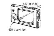
図14A,14Bは、上記実施の形態の表示装置1,2が適用されるデジタルカメラの外観を表したものである。このデジタルカメラは、例えば、フラッシュ用の発光部410、表示部420、メニュースイッチ430およびシャッターボタン440を有しており、その表示部420は、上記各実施の形態に係る表示装置1,2により構成されている。(Application example 2)
14A and 14B show the appearance of a digital camera to which the
(適用例3)
図15は、上記実施の形態の表示装置1,2が適用されるノート型パーソナルコンピュータの外観を表したものである。このノート型パーソナルコンピュータは、例えば、本体510,文字等の入力操作のためのキーボード520および画像を表示する表示部530を有しており、その表示部530は、上記各実施の形態に係る表示装置1,2により構成されている。(Application example 3)
FIG. 15 illustrates an appearance of a notebook personal computer to which the
(適用例4)
図16は、上記実施の形態の表示装置1,2が適用されるビデオカメラの外観を表したものである。このビデオカメラは、例えば、本体部610,この本体部610の前方側面に設けられた被写体撮影用のレンズ620,撮影時のスタート/ストップスイッチ630および表示部640を有しており、その表示部640は、上記各実施の形態に係る表示装置1,2により構成されている。(Application example 4)
FIG. 16 shows the appearance of a video camera to which the
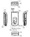
(適用例5)
図17A,17Bは、上記実施の形態の表示装置が適用される携帯電話機の外観を表したものである。この携帯電話機は、例えば、上側筐体710と下側筐体720とを連結部(ヒンジ部)730で連結したものであり、ディスプレイ740,サブディスプレイ750,ピクチャーライト760およびカメラ770を有している。そのディスプレイ740またはサブディスプレイ750は、上記各実施の形態に係る表示装置1,2により構成されている。(Application example 5)
17A and 17B show the appearance of a mobile phone to which the display device of the above embodiment is applied. For example, the mobile phone is obtained by connecting an
以上、実施の形態および変形例を挙げて本技術を説明したが、本技術は上記実施の形態等に限定されるものではなく、種々変形が可能である。例えば、上記半導体装置10では、半導体膜14Cを第1導電膜12Cに電気的に接続する場合について説明したが、半導体膜14Cは第2絶縁膜15の接続孔を介して第2導電膜17に電気的に接続するようにしてもよい(図18)。 Although the present technology has been described with the embodiment and the modification, the present technology is not limited to the above-described embodiment and the like, and various modifications can be made. For example, in the
また、上記実施の形態等では、第1電極21を陽極、第2電極24を陰極とする場合について説明したが、陽極および陰極を逆にして、第1電極21を陰極、第2電極24を陽極としてもよい。 In the above-described embodiment and the like, the case where the
更に、上記実施の形態等では、表示層が発光層を含む有機層である場合について説明したが、表示層は液晶層,発光層を含む無機層および電気泳動層等他のものであってもよい。 Furthermore, in the above-described embodiment, the case where the display layer is an organic layer including a light emitting layer has been described. However, the display layer may be a liquid crystal layer, an inorganic layer including a light emitting layer, an electrophoretic layer, or the like. Good.
加えて、上記実施の形態等において説明した各層の材料および厚み、または成膜方法および成膜条件等は限定されるものではなく、他の材料および厚みとしてもよく、または他の成膜方法および成膜条件としてもよい。 In addition, the material and thickness of each layer described in the above embodiments and the like, or the film formation method and film formation conditions are not limited, and may be other materials and thicknesses, or other film formation methods and Film forming conditions may be used.
なお、本技術は以下のような構成も取ることができる。
(1)トランジスタと共に、酸化物半導体膜と、前記酸化物半導体膜に電気的に接続された第1導電膜と、前記第1導電膜と酸化物半導体膜との間の第1絶縁膜とを備えた半導体装置。
(2)容量素子を有し、前記酸化物半導体膜および前記第1導電膜は、前記容量素子の一方の電極である前記(1)記載の半導体装置。
(3)前記容量素子は、前記酸化物半導体膜を間にして前記第1導電膜に対向する他方の電極と、前記他方の電極と前記酸化物半導体膜との間の第2絶縁膜とを有する前記(2)記載の半導体装置。
(4)前記トランジスタのゲート電極と同層に前記第1導電膜、前記トランジスタのチャネル膜と同層に前記酸化物半導体膜がそれぞれ配置され、前記第1絶縁膜は前記ゲート電極と前記チャネル膜との間に延在している前記(1)乃至(3)のうちいずれか1つ記載の半導体装置。
(5)前記トランジスタのゲート電極と前記第1導電膜、前記トランジスタのチャネル膜と前記酸化物半導体膜はそれぞれ同一の構成材料からなる前記(4)記載の半導体装置。
(6)前記第1導電膜は金属材料を含む前記(1)乃至(5)のうちいずれか1つ記載の半導体装置。
(7)前記第1導電膜と前記酸化物半導体膜とは同電位である前記(1)乃至(6)のうちいずれか1つ記載の半導体装置。
(8)表示層および前記表示層を駆動する半導体装置を備え、前記半導体装置は、トランジスタと共に、酸化物半導体膜と、前記酸化物半導体膜に電気的に接続された第1導電膜と、前記第1導電膜と酸化物半導体膜との間の第1絶縁膜とを含む表示装置。
(9)前記酸化物半導体膜および前記第1導電膜は、前記表示層を間にして対向する一対の電極のうちの一方の電極である前記(8)記載の表示装置。
(10)前記表示層は発光層を含む有機層である前記(9)記載の表示装置。
(11)前記半導体装置は容量素子を有し、前記酸化物半導体膜および前記第1導電膜は、前記容量素子の一方の電極である前記(8)記載の表示装置。
(12)表示層および前記表示層を駆動する半導体装置を有する表示装置を備え、前記半導体装置は、トランジスタと共に、酸化物半導体膜と、前記酸化物半導体膜に電気的に接続された第1導電膜と、前記第1導電膜と酸化物半導体膜との間の第1絶縁膜とを有する電子機器。In addition, this technique can also take the following structures.
(1) Along with the transistor, an oxide semiconductor film, a first conductive film electrically connected to the oxide semiconductor film, and a first insulating film between the first conductive film and the oxide semiconductor film A semiconductor device provided.
(2) The semiconductor device according to (1), further including a capacitive element, wherein the oxide semiconductor film and the first conductive film are one electrode of the capacitive element.
(3) The capacitive element includes the other electrode facing the first conductive film with the oxide semiconductor film in between, and a second insulating film between the other electrode and the oxide semiconductor film. The semiconductor device according to (2).
(4) The first conductive film is disposed in the same layer as the gate electrode of the transistor, the oxide semiconductor film is disposed in the same layer as the channel film of the transistor, and the first insulating film is the gate electrode and the channel film. The semiconductor device as described in any one of said (1) thru | or (3) currently extended between.
(5) The semiconductor device according to (4), wherein the gate electrode and the first conductive film of the transistor, the channel film of the transistor, and the oxide semiconductor film are made of the same constituent material.
(6) The semiconductor device according to any one of (1) to (5), wherein the first conductive film includes a metal material.
(7) The semiconductor device according to any one of (1) to (6), wherein the first conductive film and the oxide semiconductor film have the same potential.
(8) A display layer and a semiconductor device that drives the display layer, the semiconductor device, together with a transistor, an oxide semiconductor film, a first conductive film electrically connected to the oxide semiconductor film, A display device including a first conductive film and a first insulating film between the oxide semiconductor film.
(9) The display device according to (8), wherein the oxide semiconductor film and the first conductive film are one of a pair of electrodes facing each other with the display layer interposed therebetween.
(10) The display device according to (9), wherein the display layer is an organic layer including a light emitting layer.
(11) The display device according to (8), wherein the semiconductor device includes a capacitor, and the oxide semiconductor film and the first conductive film are one electrode of the capacitor.
(12) A display device having a display layer and a semiconductor device that drives the display layer, the semiconductor device, together with a transistor, an oxide semiconductor film, and a first conductive electrically connected to the oxide semiconductor film An electronic apparatus having a film and a first insulating film between the first conductive film and the oxide semiconductor film.
1,2・・・表示装置、10・・・半導体装置、11・・・基板、10T・・・トランジスタ、10C・・・容量素子、12T・・・ゲート電極、12C・・・第1導電膜、13・・・第1絶縁膜、14T・・・チャネル膜、14C・・・半導体膜、15・・・第2絶縁膜、16A,16B・・・ソース・ドレイン電極、16C・・・配線、17・・・第2導電膜、20・・・有機EL素子、21・・・第1電極、22・・・隔壁、23・・・有機層、24・・・第2電極、25・・・対向基板。 DESCRIPTION OF
Claims (12)
Translated fromJapanese酸化物半導体膜および前記酸化物半導体膜に電気的に接続された第1導電膜が一方の電極、前記酸化物半導体膜を間にして前記第1導電膜に対向する第2導電膜が他方の電極を構成する容量素子と、
前記第1導電膜と前記酸化物半導体膜との間の第1絶縁膜と、
前記第2導電膜と前記酸化物半導体膜との間の第2絶縁膜とを備え、
前記ゲート電極と同層に前記第1導電膜、前記チャネル膜と同層に前記酸化物半導体膜がそれぞれ配置され、前記第1絶縁膜は前記ゲート電極と前記チャネル膜との間に延在している
半導体装置。A transistorhaving a gate electrode and a channel film facing the gate electrode;
The first conductive film electrically connected to the oxide semiconductor filmand the oxide semiconductor filmis one electrode, and the second conductive film facing the first conductive film with the oxide semiconductor film in between is the other A capacitive element constituting an electrode;
A first insulating film between the first conductive film and the oxide semiconductor film;
A second insulating film between the second conductive film and the oxide semiconductor film,
The first conductive film is disposed in the same layer as the gate electrode, and the oxide semiconductor film is disposed in the same layer as the channel film. The first insulating film extends between the gate electrode and the channel film. in which the semiconductor device.
請求項1記載の半導体装置。The first conductive film and the gate electrode, the channel layer and the oxide semiconductor film is a semiconductor device according to claim1, wherein each composed of the same constituent material.
請求項1または2記載の半導体装置。Wherein the first conductive film semiconductor device according to claim 1or 2 wherein comprises a metal material.
請求項1乃至3のうちいずれか1つ記載の半導体装置。Wherein the said oxide semiconductor film first conductive film semiconductor device accordingany one of claims 1to 3 have the same potential.
請求項1乃至4のうちいずれか1つ記載の半導体装置。The semiconductor device according to claim 1.
請求項5記載の半導体装置。The semiconductor device according to claim 5.
前記半導体装置は、
ゲート電極および前記ゲート電極に対向するチャネル膜を有するトランジスタと、
酸化物半導体膜および前記酸化物半導体膜に電気的に接続された第1導電膜が一方の電極、前記酸化物半導体膜を間にして前記第1導電膜に対向する第2導電膜が他方の電極を構成する容量素子と、
前記第1導電膜と前記酸化物半導体膜との間の第1絶縁膜と、
前記第2導電膜と前記酸化物半導体膜との間の第2絶縁膜とを備え、
前記ゲート電極と同層に前記第1導電膜、前記チャネル膜と同層に前記酸化物半導体膜がそれぞれ配置され、前記第1絶縁膜は前記ゲート電極と前記チャネル膜との間に延在している
表示装置。A display layer and a semiconductor device for driving the display layer;
The semiconductor device includes:
A transistorhaving a gate electrode and a channel film facing the gate electrode;
The first conductive film electrically connected to the oxide semiconductor filmand the oxide semiconductor filmis one electrode, and the second conductive film facing the first conductive film with the oxide semiconductor film in between is the other A capacitive element constituting an electrode;
A first insulating film between the first conductive film and the oxide semiconductor film;
A second insulating film between the second conductive film and the oxide semiconductor film,
The first conductive film is disposed in the same layer as the gate electrode, and the oxide semiconductor film is disposed in the same layer as the channel film. The first insulating film extends between the gate electrode and the channel film. and it has a display device.
前記第1電極に対向する第2電極と、
前記第1電極と前記第2電極との間の表示層と、
ゲート電極および前記ゲート電極に対向するチャネル膜を有し、前記表示層を駆動するトランジスタと、
前記第1導電膜と前記酸化物半導体膜との間の第1絶縁膜とを備え、
前記ゲート電極と同層に前記第1導電膜、前記チャネル膜と同層に前記酸化物半導体膜がそれぞれ配置され、前記第1絶縁膜は前記ゲート電極と前記チャネル膜との間に延在している
表示装置。A first electrode composed of an oxide semiconductor film and a first conductive film electrically connected to the oxide semiconductor film;
A second electrode facing the first electrode;
A display layer between the first electrode and the second electrode;
A transistor having a gate electrode and a channel film facing the gate electrode and driving the display layer;
A first insulating film between the first conductive film and the oxide semiconductor film,
The first conductive film is disposed in the same layer as the gate electrode, and the oxide semiconductor film is disposed in the same layer as the channel film. The first insulating film extends between the gate electrode and the channel film. and it has a display device.
請求項7または8記載の表示装置。The display device according to claim7 , wherein the display layer is an organic layer including a light emitting layer.
請求項7乃至9のうちいずれか1つ記載の半導体装置。10. The semiconductor device according to any one of claims 7 to 9.
前記半導体装置は、
ゲート電極および前記ゲート電極に対向するチャネル膜を有するトランジスタと、
酸化物半導体膜および前記酸化物半導体膜に電気的に接続された第1導電膜が一方の電極、前記酸化物半導体膜を間にして前記第1導電膜に対向する第2導電膜が他方の電極を構成する容量素子と、
前記第1導電膜と前記酸化物半導体膜との間の第1絶縁膜と、
前記第2導電膜と前記酸化物半導体膜との間の第2絶縁膜とを備え、
前記ゲート電極と同層に前記第1導電膜、前記チャネル膜と同層に前記酸化物半導体膜がそれぞれ配置され、前記第1絶縁膜は前記ゲート電極と前記チャネル膜との間に延在している
電子機器。A display device having a display layer and a semiconductor device for driving the display layer;
The semiconductor device includes:
A transistorhaving a gate electrode and a channel film facing the gate electrode;
The first conductive film electrically connected to the oxide semiconductor filmand the oxide semiconductor filmis one electrode, and the second conductive film facing the first conductive film with the oxide semiconductor film in between is the other A capacitive element constituting an electrode;
A first insulating film between the first conductive film and the oxide semiconductor film;
A second insulating film between the second conductive film and the oxide semiconductor film,
The first conductive film is disposed in the same layer as the gate electrode, and the oxide semiconductor film is disposed in the same layer as the channel film. The first insulating film extends between the gate electrode and the channel film. and are electronic devices.
前記表示装置は、
酸化物半導体膜および前記酸化物半導体膜に電気的に接続された第1導電膜により構成された第1電極と、
前記第1電極に対向する第2電極と、
前記第1電極と前記第2電極との間の表示層と、
ゲート電極および前記ゲート電極に対向するチャネル膜を有し、前記表示層を駆動するトランジスタと、
前記第1導電膜と前記酸化物半導体膜との間の第1絶縁膜とを備え、
前記ゲート電極と同層に前記第1導電膜、前記チャネル膜と同層に前記酸化物半導体膜がそれぞれ配置され、前記第1絶縁膜は前記ゲート電極と前記チャネル膜との間に延在している
電子機器。A display device,
The display device
A first electrode composed of an oxide semiconductor film and a first conductive film electrically connected to the oxide semiconductor film;
A second electrode facing the first electrode;
A display layer between the first electrode and the second electrode;
A transistor having a gate electrode and a channel film facing the gate electrode and driving the display layer;
A first insulating film between the first conductive film and the oxide semiconductor film,
The first conductive film is disposed in the same layer as the gate electrode, and the oxide semiconductor film is disposed in the same layer as the channel film. The first insulating film extends between the gate electrode and the channel film. and are electronic devices.
Priority Applications (5)
| Application Number | Priority Date | Filing Date | Title |
|---|---|---|---|
| JP2013066219AJP6083089B2 (en) | 2013-03-27 | 2013-03-27 | Semiconductor device, display device and electronic apparatus |
| TW103105342ATW201438253A (en) | 2013-03-27 | 2014-02-18 | Semiconductor device, display unit and electronic device |
| KR1020140023090AKR20140118739A (en) | 2013-03-27 | 2014-02-27 | Semiconductor device, display unit, and electronic apparatus |
| US14/202,852US9178074B2 (en) | 2013-03-27 | 2014-03-10 | Semiconductor device, display unit, and electronic apparatus |
| CN201410105909.3ACN104078510A (en) | 2013-03-27 | 2014-03-20 | Semiconductor device, display unit, and electronic apparatus |
Applications Claiming Priority (1)
| Application Number | Priority Date | Filing Date | Title |
|---|---|---|---|
| JP2013066219AJP6083089B2 (en) | 2013-03-27 | 2013-03-27 | Semiconductor device, display device and electronic apparatus |
Publications (3)
| Publication Number | Publication Date |
|---|---|
| JP2014192319A JP2014192319A (en) | 2014-10-06 |
| JP2014192319A5 JP2014192319A5 (en) | 2015-08-06 |
| JP6083089B2true JP6083089B2 (en) | 2017-02-22 |
Family
ID=51599671
Family Applications (1)
| Application Number | Title | Priority Date | Filing Date |
|---|---|---|---|
| JP2013066219AActiveJP6083089B2 (en) | 2013-03-27 | 2013-03-27 | Semiconductor device, display device and electronic apparatus |
Country Status (5)
| Country | Link |
|---|---|
| US (1) | US9178074B2 (en) |
| JP (1) | JP6083089B2 (en) |
| KR (1) | KR20140118739A (en) |
| CN (1) | CN104078510A (en) |
| TW (1) | TW201438253A (en) |
Families Citing this family (1)
| Publication number | Priority date | Publication date | Assignee | Title |
|---|---|---|---|---|
| TWI577031B (en)* | 2014-11-04 | 2017-04-01 | 群創光電股份有限公司 | Display device |
Family Cites Families (25)
| Publication number | Priority date | Publication date | Assignee | Title |
|---|---|---|---|---|
| KR101652693B1 (en)* | 2008-10-03 | 2016-09-01 | 가부시키가이샤 한도오따이 에네루기 켄큐쇼 | Display device |
| EP2172977A1 (en)* | 2008-10-03 | 2010-04-07 | Semiconductor Energy Laboratory Co., Ltd. | Display device |
| CN101714546B (en)* | 2008-10-03 | 2014-05-14 | 株式会社半导体能源研究所 | Display device and manufacturing method thereof |
| US8106400B2 (en)* | 2008-10-24 | 2012-01-31 | Semiconductor Energy Laboratory Co., Ltd. | Semiconductor device and method for manufacturing the same |
| KR101914404B1 (en)* | 2008-11-21 | 2018-11-01 | 가부시키가이샤 한도오따이 에네루기 켄큐쇼 | Semiconductor device |
| CN103456794B (en) | 2008-12-19 | 2016-08-10 | 株式会社半导体能源研究所 | How Transistors Are Made |
| EP2515337B1 (en)* | 2008-12-24 | 2016-02-24 | Semiconductor Energy Laboratory Co., Ltd. | Driver circuit and semiconductor device |
| JP2010222214A (en) | 2009-03-25 | 2010-10-07 | Idemitsu Kosan Co Ltd | Metal oxide thin film and manufacturing method thereof |
| WO2011043194A1 (en)* | 2009-10-09 | 2011-04-14 | Semiconductor Energy Laboratory Co., Ltd. | Semiconductor device and method for manufacturing the same |
| JP5599026B2 (en) | 2009-10-23 | 2014-10-01 | キヤノン株式会社 | Thin film transistor manufacturing method |
| KR101073272B1 (en) | 2009-11-04 | 2011-10-12 | 삼성모바일디스플레이주식회사 | Method of manufacturing organic light emitting display device |
| CN102652330B (en)* | 2009-12-09 | 2014-09-17 | 夏普株式会社 | Semiconductor device and method for producing same |
| JP5095865B2 (en)* | 2009-12-21 | 2012-12-12 | シャープ株式会社 | Active matrix substrate, display panel including the same, and method for manufacturing active matrix substrate |
| WO2011086905A1 (en)* | 2010-01-13 | 2011-07-21 | シャープ株式会社 | Active matrix substrate and manufacturing method thereof |
| US8698152B2 (en)* | 2010-05-24 | 2014-04-15 | Sharp Kabushiki Kaisha | Display panel and thin film transistor substrate |
| KR101783352B1 (en)* | 2010-06-17 | 2017-10-10 | 삼성디스플레이 주식회사 | Flat panel display apparatus and manufacturing method of the same |
| JP5806043B2 (en)* | 2010-08-27 | 2015-11-10 | 株式会社半導体エネルギー研究所 | Method for manufacturing semiconductor device |
| US8558960B2 (en)* | 2010-09-13 | 2013-10-15 | Semiconductor Energy Laboratory Co., Ltd. | Liquid crystal display device and method for manufacturing the same |
| KR101736319B1 (en)* | 2010-12-14 | 2017-05-17 | 삼성디스플레이 주식회사 | Organic light emitting display device and manufacturing method of the same |
| TWI544525B (en)* | 2011-01-21 | 2016-08-01 | 半導體能源研究所股份有限公司 | Semiconductor device and method of manufacturing same |
| JP5825812B2 (en)* | 2011-03-24 | 2015-12-02 | 株式会社Joled | Manufacturing method of display device |
| KR20140021118A (en)* | 2012-08-07 | 2014-02-20 | 삼성디스플레이 주식회사 | Display device and method of manufacturing the same |
| KR101989058B1 (en)* | 2012-10-24 | 2019-06-14 | 삼성디스플레이 주식회사 | Vapor deposition apparatus having the same, method for forming thin film using the same and method for manufacturing organic light emitting display apparatus |
| KR102028025B1 (en)* | 2012-11-13 | 2019-10-04 | 삼성디스플레이 주식회사 | Organic light emitting display apparatus and method of manufacturing the same |
| KR102091663B1 (en)* | 2013-06-28 | 2020-03-23 | 삼성디스플레이 주식회사 | Thin film transistor and organic light emitting diode display |
- 2013
- 2013-03-27JPJP2013066219Apatent/JP6083089B2/enactiveActive
- 2014
- 2014-02-18TWTW103105342Apatent/TW201438253A/enunknown
- 2014-02-27KRKR1020140023090Apatent/KR20140118739A/ennot_activeWithdrawn
- 2014-03-10USUS14/202,852patent/US9178074B2/enactiveActive
- 2014-03-20CNCN201410105909.3Apatent/CN104078510A/enactivePending
Also Published As
| Publication number | Publication date |
|---|---|
| US9178074B2 (en) | 2015-11-03 |
| KR20140118739A (en) | 2014-10-08 |
| US20140291639A1 (en) | 2014-10-02 |
| CN104078510A (en) | 2014-10-01 |
| TW201438253A (en) | 2014-10-01 |
| JP2014192319A (en) | 2014-10-06 |
Similar Documents
| Publication | Publication Date | Title |
|---|---|---|
| JP4626659B2 (en) | Display device | |
| US8748882B2 (en) | Thin film transistor, electronic device, display device, and method of manufacturing thin film transistor | |
| JP4752925B2 (en) | Thin film transistor and display device | |
| JP5743064B2 (en) | THIN FILM TRANSISTOR, MANUFACTURING METHOD THEREOF, AND DISPLAY DEVICE | |
| US20110215328A1 (en) | Thin film transistor, method of manufacturing the thin film transistor, and display device | |
| JP5766481B2 (en) | Display device and electronic device | |
| JP5737550B2 (en) | Display device, display device manufacturing method, and electronic apparatus | |
| JP2010182819A (en) | Thin-film transistor, and display device | |
| TW201123421A (en) | Semiconductor device and manufacturing method thereof | |
| JP2013161895A (en) | Thin-film transistor, display device, and electronic equipment | |
| US9252160B2 (en) | Thin film transistor array panel and method of manufacturing the same | |
| US8816352B2 (en) | Display device and electronic device | |
| JP2015023161A (en) | Thin film transistor, manufacturing method of the same and electronic apparatus | |
| JP2014229814A (en) | Thin-film transistor, display device, and electronic apparatus | |
| JP2013206919A (en) | Thin film transistor, manufacturing method of the same and display device | |
| JP6083089B2 (en) | Semiconductor device, display device and electronic apparatus | |
| JP2013149827A (en) | Thin-film transistor, method of manufacturing the same, display unit, and electronic apparatus | |
| US9502492B2 (en) | Semiconductor device, method of manufacturing the same, display unit, and electronic apparatus | |
| US9219084B2 (en) | Display device including a thin film transistor having wiring and electrodes with different ionization tendencies | |
| CN120568814A (en) | Transistor and display device including the same |
Legal Events
| Date | Code | Title | Description |
|---|---|---|---|
| A711 | Notification of change in applicant | Free format text:JAPANESE INTERMEDIATE CODE: A712 Effective date:20150327 | |
| A521 | Request for written amendment filed | Free format text:JAPANESE INTERMEDIATE CODE: A523 Effective date:20150617 | |
| A621 | Written request for application examination | Free format text:JAPANESE INTERMEDIATE CODE: A621 Effective date:20150617 | |
| A521 | Request for written amendment filed | Free format text:JAPANESE INTERMEDIATE CODE: A523 Effective date:20151001 | |
| A977 | Report on retrieval | Free format text:JAPANESE INTERMEDIATE CODE: A971007 Effective date:20160623 | |
| A131 | Notification of reasons for refusal | Free format text:JAPANESE INTERMEDIATE CODE: A131 Effective date:20160726 | |
| A521 | Request for written amendment filed | Free format text:JAPANESE INTERMEDIATE CODE: A523 Effective date:20160905 | |
| TRDD | Decision of grant or rejection written | ||
| A01 | Written decision to grant a patent or to grant a registration (utility model) | Free format text:JAPANESE INTERMEDIATE CODE: A01 Effective date:20161220 | |
| A61 | First payment of annual fees (during grant procedure) | Free format text:JAPANESE INTERMEDIATE CODE: A61 Effective date:20170106 | |
| R150 | Certificate of patent or registration of utility model | Ref document number:6083089 Country of ref document:JP Free format text:JAPANESE INTERMEDIATE CODE: R150 | |
| R250 | Receipt of annual fees | Free format text:JAPANESE INTERMEDIATE CODE: R250 | |
| R250 | Receipt of annual fees | Free format text:JAPANESE INTERMEDIATE CODE: R250 | |
| R250 | Receipt of annual fees | Free format text:JAPANESE INTERMEDIATE CODE: R250 | |
| R250 | Receipt of annual fees | Free format text:JAPANESE INTERMEDIATE CODE: R250 | |
| S303 | Written request for registration of pledge or change of pledge | Free format text:JAPANESE INTERMEDIATE CODE: R316303 | |
| R350 | Written notification of registration of transfer | Free format text:JAPANESE INTERMEDIATE CODE: R350 | |
| S803 | Written request for registration of cancellation of provisional registration | Free format text:JAPANESE INTERMEDIATE CODE: R316803 | |
| R350 | Written notification of registration of transfer | Free format text:JAPANESE INTERMEDIATE CODE: R350 | |
| R250 | Receipt of annual fees | Free format text:JAPANESE INTERMEDIATE CODE: R250 | |
| S111 | Request for change of ownership or part of ownership | Free format text:JAPANESE INTERMEDIATE CODE: R313113 | |
| R350 | Written notification of registration of transfer | Free format text:JAPANESE INTERMEDIATE CODE: R350 |