JP6082028B2 - Improvements in accelerometers - Google Patents
Improvements in accelerometersDownload PDFInfo
- Publication number
- JP6082028B2 JP6082028B2JP2014551670AJP2014551670AJP6082028B2JP 6082028 B2JP6082028 B2JP 6082028B2JP 2014551670 AJP2014551670 AJP 2014551670AJP 2014551670 AJP2014551670 AJP 2014551670AJP 6082028 B2JP6082028 B2JP 6082028B2
- Authority
- JP
- Japan
- Prior art keywords
- beams
- accelerometer
- proof mass
- actuator
- bias
- Prior art date
- Legal status (The legal status is an assumption and is not a legal conclusion. Google has not performed a legal analysis and makes no representation as to the accuracy of the status listed.)
- Expired - Fee Related
Links
- 239000000758substrateSubstances0.000claimsdescription11
- 230000033001locomotionEffects0.000claimsdescription10
- 230000001133accelerationEffects0.000claimsdescription8
- 229910052710siliconInorganic materials0.000claimsdescription8
- 239000010703siliconSubstances0.000claimsdescription8
- 230000003287optical effectEffects0.000claimsdescription7
- 239000000835fiberSubstances0.000claimsdescription6
- PCHJSUWPFVWCPO-UHFFFAOYSA-NgoldChemical compound[Au]PCHJSUWPFVWCPO-UHFFFAOYSA-N0.000claimsdescription3
- 239000010931goldSubstances0.000claimsdescription3
- 229910052737goldInorganic materials0.000claimsdescription3
- 238000002310reflectometryMethods0.000claimsdescription2
- 230000035945sensitivityEffects0.000description9
- 230000003321amplificationEffects0.000description8
- 238000003199nucleic acid amplification methodMethods0.000description8
- 239000013307optical fiberSubstances0.000description8
- XUIMIQQOPSSXEZ-UHFFFAOYSA-NSiliconChemical compound[Si]XUIMIQQOPSSXEZ-UHFFFAOYSA-N0.000description7
- 238000000034methodMethods0.000description5
- 230000008901benefitEffects0.000description3
- 230000008859changeEffects0.000description3
- 239000011248coating agentSubstances0.000description3
- 238000000576coating methodMethods0.000description3
- 238000013461designMethods0.000description3
- 238000001514detection methodMethods0.000description3
- 238000005259measurementMethods0.000description3
- 230000004044responseEffects0.000description3
- 238000006073displacement reactionMethods0.000description2
- 230000000694effectsEffects0.000description2
- 239000000463materialSubstances0.000description2
- 238000001020plasma etchingMethods0.000description2
- 239000004593EpoxySubstances0.000description1
- 230000003667anti-reflective effectEffects0.000description1
- 238000005452bendingMethods0.000description1
- 230000005540biological transmissionEffects0.000description1
- 230000008878couplingEffects0.000description1
- 238000010168coupling processMethods0.000description1
- 238000005859coupling reactionMethods0.000description1
- 230000001186cumulative effectEffects0.000description1
- 238000013016dampingMethods0.000description1
- 238000005516engineering processMethods0.000description1
- 239000002360explosiveSubstances0.000description1
- 238000009501film coatingMethods0.000description1
- 238000005286illuminationMethods0.000description1
- 239000012212insulatorSubstances0.000description1
- JEIPFZHSYJVQDO-UHFFFAOYSA-Niron(III) oxideInorganic materialsO=[Fe]O[Fe]=OJEIPFZHSYJVQDO-UHFFFAOYSA-N0.000description1
- 238000004519manufacturing processMethods0.000description1
- 239000002184metalSubstances0.000description1
- 229910052751metalInorganic materials0.000description1
- 238000010295mobile communicationMethods0.000description1
- 230000007935neutral effectEffects0.000description1
- 238000000206photolithographyMethods0.000description1
- 230000008569processEffects0.000description1
- 238000012545processingMethods0.000description1
- 238000000926separation methodMethods0.000description1
- 239000007787solidSubstances0.000description1
- 238000004544sputter depositionMethods0.000description1
- 238000012360testing methodMethods0.000description1
- 239000010409thin filmSubstances0.000description1
- 238000000427thin-film depositionMethods0.000description1
- 235000012431wafersNutrition0.000description1
- 238000001039wet etchingMethods0.000description1
Images


Classifications
- G—PHYSICS
- G01—MEASURING; TESTING
- G01C—MEASURING DISTANCES, LEVELS OR BEARINGS; SURVEYING; NAVIGATION; GYROSCOPIC INSTRUMENTS; PHOTOGRAMMETRY OR VIDEOGRAMMETRY
- G01C19/00—Gyroscopes; Turn-sensitive devices using vibrating masses; Turn-sensitive devices without moving masses; Measuring angular rate using gyroscopic effects
- G01C19/56—Turn-sensitive devices using vibrating masses, e.g. vibratory angular rate sensors based on Coriolis forces
- G01C19/5642—Turn-sensitive devices using vibrating masses, e.g. vibratory angular rate sensors based on Coriolis forces using vibrating bars or beams
- G—PHYSICS
- G01—MEASURING; TESTING
- G01P—MEASURING LINEAR OR ANGULAR SPEED, ACCELERATION, DECELERATION, OR SHOCK; INDICATING PRESENCE, ABSENCE, OR DIRECTION, OF MOVEMENT
- G01P15/00—Measuring acceleration; Measuring deceleration; Measuring shock, i.e. sudden change of acceleration
- G01P15/02—Measuring acceleration; Measuring deceleration; Measuring shock, i.e. sudden change of acceleration by making use of inertia forces using solid seismic masses
- G01P15/08—Measuring acceleration; Measuring deceleration; Measuring shock, i.e. sudden change of acceleration by making use of inertia forces using solid seismic masses with conversion into electric or magnetic values
- G01P15/0802—Details
- G—PHYSICS
- G01—MEASURING; TESTING
- G01P—MEASURING LINEAR OR ANGULAR SPEED, ACCELERATION, DECELERATION, OR SHOCK; INDICATING PRESENCE, ABSENCE, OR DIRECTION, OF MOVEMENT
- G01P15/00—Measuring acceleration; Measuring deceleration; Measuring shock, i.e. sudden change of acceleration
- G01P15/02—Measuring acceleration; Measuring deceleration; Measuring shock, i.e. sudden change of acceleration by making use of inertia forces using solid seismic masses
- G01P15/08—Measuring acceleration; Measuring deceleration; Measuring shock, i.e. sudden change of acceleration by making use of inertia forces using solid seismic masses with conversion into electric or magnetic values
- G01P15/093—Measuring acceleration; Measuring deceleration; Measuring shock, i.e. sudden change of acceleration by making use of inertia forces using solid seismic masses with conversion into electric or magnetic values by photoelectric pick-up
- G—PHYSICS
- G01—MEASURING; TESTING
- G01P—MEASURING LINEAR OR ANGULAR SPEED, ACCELERATION, DECELERATION, OR SHOCK; INDICATING PRESENCE, ABSENCE, OR DIRECTION, OF MOVEMENT
- G01P15/00—Measuring acceleration; Measuring deceleration; Measuring shock, i.e. sudden change of acceleration
- G01P15/02—Measuring acceleration; Measuring deceleration; Measuring shock, i.e. sudden change of acceleration by making use of inertia forces using solid seismic masses
- G01P15/08—Measuring acceleration; Measuring deceleration; Measuring shock, i.e. sudden change of acceleration by making use of inertia forces using solid seismic masses with conversion into electric or magnetic values
- G01P15/125—Measuring acceleration; Measuring deceleration; Measuring shock, i.e. sudden change of acceleration by making use of inertia forces using solid seismic masses with conversion into electric or magnetic values by capacitive pick-up
- G—PHYSICS
- G01—MEASURING; TESTING
- G01C—MEASURING DISTANCES, LEVELS OR BEARINGS; SURVEYING; NAVIGATION; GYROSCOPIC INSTRUMENTS; PHOTOGRAMMETRY OR VIDEOGRAMMETRY
- G01C19/00—Gyroscopes; Turn-sensitive devices using vibrating masses; Turn-sensitive devices without moving masses; Measuring angular rate using gyroscopic effects
- G01C19/56—Turn-sensitive devices using vibrating masses, e.g. vibratory angular rate sensors based on Coriolis forces
- G01C19/5607—Turn-sensitive devices using vibrating masses, e.g. vibratory angular rate sensors based on Coriolis forces using vibrating tuning forks
- G—PHYSICS
- G01—MEASURING; TESTING
- G01C—MEASURING DISTANCES, LEVELS OR BEARINGS; SURVEYING; NAVIGATION; GYROSCOPIC INSTRUMENTS; PHOTOGRAMMETRY OR VIDEOGRAMMETRY
- G01C19/00—Gyroscopes; Turn-sensitive devices using vibrating masses; Turn-sensitive devices without moving masses; Measuring angular rate using gyroscopic effects
- G01C19/56—Turn-sensitive devices using vibrating masses, e.g. vibratory angular rate sensors based on Coriolis forces
- G01C19/5642—Turn-sensitive devices using vibrating masses, e.g. vibratory angular rate sensors based on Coriolis forces using vibrating bars or beams
- G01C19/5649—Signal processing
- G—PHYSICS
- G01—MEASURING; TESTING
- G01C—MEASURING DISTANCES, LEVELS OR BEARINGS; SURVEYING; NAVIGATION; GYROSCOPIC INSTRUMENTS; PHOTOGRAMMETRY OR VIDEOGRAMMETRY
- G01C19/00—Gyroscopes; Turn-sensitive devices using vibrating masses; Turn-sensitive devices without moving masses; Measuring angular rate using gyroscopic effects
- G01C19/56—Turn-sensitive devices using vibrating masses, e.g. vibratory angular rate sensors based on Coriolis forces
- G01C19/5719—Turn-sensitive devices using vibrating masses, e.g. vibratory angular rate sensors based on Coriolis forces using planar vibrating masses driven in a translation vibration along an axis
- G—PHYSICS
- G01—MEASURING; TESTING
- G01P—MEASURING LINEAR OR ANGULAR SPEED, ACCELERATION, DECELERATION, OR SHOCK; INDICATING PRESENCE, ABSENCE, OR DIRECTION, OF MOVEMENT
- G01P15/00—Measuring acceleration; Measuring deceleration; Measuring shock, i.e. sudden change of acceleration
- G01P15/02—Measuring acceleration; Measuring deceleration; Measuring shock, i.e. sudden change of acceleration by making use of inertia forces using solid seismic masses
- G01P15/08—Measuring acceleration; Measuring deceleration; Measuring shock, i.e. sudden change of acceleration by making use of inertia forces using solid seismic masses with conversion into electric or magnetic values
- G01P2015/0805—Measuring acceleration; Measuring deceleration; Measuring shock, i.e. sudden change of acceleration by making use of inertia forces using solid seismic masses with conversion into electric or magnetic values being provided with a particular type of spring-mass-system for defining the displacement of a seismic mass due to an external acceleration
- G01P2015/0808—Measuring acceleration; Measuring deceleration; Measuring shock, i.e. sudden change of acceleration by making use of inertia forces using solid seismic masses with conversion into electric or magnetic values being provided with a particular type of spring-mass-system for defining the displacement of a seismic mass due to an external acceleration for defining in-plane movement of the mass, i.e. movement of the mass in the plane of the substrate
- G01P2015/0811—Measuring acceleration; Measuring deceleration; Measuring shock, i.e. sudden change of acceleration by making use of inertia forces using solid seismic masses with conversion into electric or magnetic values being provided with a particular type of spring-mass-system for defining the displacement of a seismic mass due to an external acceleration for defining in-plane movement of the mass, i.e. movement of the mass in the plane of the substrate for one single degree of freedom of movement of the mass
- G01P2015/0814—Measuring acceleration; Measuring deceleration; Measuring shock, i.e. sudden change of acceleration by making use of inertia forces using solid seismic masses with conversion into electric or magnetic values being provided with a particular type of spring-mass-system for defining the displacement of a seismic mass due to an external acceleration for defining in-plane movement of the mass, i.e. movement of the mass in the plane of the substrate for one single degree of freedom of movement of the mass for translational movement of the mass, e.g. shuttle type
Landscapes
- Physics & Mathematics (AREA)
- General Physics & Mathematics (AREA)
- Engineering & Computer Science (AREA)
- Radar, Positioning & Navigation (AREA)
- Remote Sensing (AREA)
- Micromachines (AREA)
- Pressure Sensors (AREA)
Description
Translated fromJapanese本発明は、加速度計およびそのようなものに関する。 The present invention relates to accelerometers and the like.
加速度計は通常、ばね上の減衰されるプルーフマスを使用する。外部加速の影響の下、プルーフマスはその中立位置から偏る。この偏りが測定され、そこから加速度が算出される。一般的に、固定された電極のセットとプルーフマスに取り付けられた電極のセットの間の静電容量が測定される。この方法は簡単で確実、そして安価である。 Accelerometers typically use a proof mass that is damped over a spring. Under the influence of external acceleration, the proof mass is biased from its neutral position. This bias is measured, and acceleration is calculated therefrom. In general, the capacitance between a fixed set of electrodes and a set of electrodes attached to a proof mass is measured. This method is simple, reliable and inexpensive.
現代の加速度計は、しばしば、小型のマイクロ電気機械システム(MEMS)であり、ほとんどプルーフマス(震動性マスとしても知られている)を備えた片持ちビームのみからなる。減衰は、装置内にシールされた残留ガスの結果生じる。そのような装置を作製するための一般的な方法は、単一のシリコンブロックから構成要素をエッチングすることである。プルーフマスが移動するとき、このプルーフマスとプルーフマスが懸架される片持ちビームの基部との間の変位が、測定される。 Modern accelerometers are often small microelectromechanical systems (MEMS), consisting mostly of cantilevered beams with proof masses (also known as seismic masses). Damping occurs as a result of residual gas sealed in the device. A common method for making such a device is to etch the components from a single silicon block. As the proof mass moves, the displacement between the proof mass and the base of the cantilever beam on which the proof mass is suspended is measured.
MEMS加速度計は、安価で小型であるため、しばしば、数多くの現代の装置内の構成要素として使用される。ソリッドステート加速度計は、たとえば数多くの現在のスマートホンにおいて見出され、それにより、スマートホンのソフトウエアがその配向を検出し、それにしたがってディスプレイを回転させることができる。 Because MEMS accelerometers are inexpensive and small, they are often used as a component in many modern devices. Solid state accelerometers are found, for example, in a number of current smart phones so that smart phone software can detect its orientation and rotate the display accordingly.
そのような装置の感度は限定されており、向上した感度を有するMEMSタイプの装置を作り出すことが有利である。したがって、本発明は、固定された基板内にプルーフマスを備える加速度計であって、プルーフマスが1つまたは複数のVビームによって基板に接続され、基板の加速度が、Vビームまたはその複数のビームの偏りを測定することによって決定される、加速度計を提供する。 The sensitivity of such devices is limited and it is advantageous to create MEMS type devices with improved sensitivity. Accordingly, the present invention is an accelerometer comprising a proof mass in a fixed substrate, wherein the proof mass is connected to the substrate by one or more V beams, and the acceleration of the substrate is the V beam or the plurality of beams. An accelerometer is provided that is determined by measuring the bias of the.
そのような構成は、偏りの増幅を導き、それによって加速度に対する装置の感度を高める。 Such a configuration leads to bias amplification, thereby increasing the sensitivity of the device to acceleration.
プルーフマスが固定された基板に対して移動するとき、Vビームは、中央において反るまたは曲がることによって偏り、この偏りが検出器によって取り上げられる。幾何学的に、Vビームの偏りはプルーフマスの移動より大きいため、加速度計には増幅が組み込まれ、それによって加速度計の感度をより高くする。 As the proof mass moves relative to the fixed substrate, the V-beam is deflected by warping or bending in the center, and this bias is picked up by the detector. Geometrically, the V-beam bias is greater than the movement of the proof mass, so amplification is built into the accelerometer, thereby making the accelerometer more sensitive.
検出は、静電容量の変動を検出することによるもの、または電気光学式検出によるものでよい。検出方法が光学式である場合、金または別の適切な反射材料などの光学的反射性コーティングをVビームの頂点に施して感度を強めることが可能である。これは、偏りを測定するために使用され得るファブリペロー干渉計の1つの鏡を形成する。 The detection may be by detecting a change in capacitance or by electro-optical detection. If the detection method is optical, an optically reflective coating such as gold or another suitable reflective material can be applied to the apex of the V-beam to increase sensitivity. This forms one mirror of a Fabry-Perot interferometer that can be used to measure bias.
1つのVビームが使用される場合、ファブリペロー空洞が、Vビーム鏡および装置に応答する光ファイバの端部からの反射によって形成され得る。Vビームは、連接される必要はない。直線または反ったビームは、これが予想可能な方法で適切な方向に偏る限り使用され得る。 If a single V-beam is used, a Fabry-Perot cavity can be formed by reflection from the end of the optical fiber in response to the V-beam mirror and device. V beams need not be articulated. A straight or warped beam can be used as long as it deviates in the proper direction in a predictable manner.
ファブリペロー空洞は、2つの隣接するシリコンブロックの対向する側壁間に形成され得る。シリコンは、1.13μmを超える光波長において光学的に透過性であり、そのため赤外領域内の適切な波長、たとえば1.55μmを選択することにより、空洞は、ブロックの1つを通って入る光によって照らされ得る。ブロックの外側側壁からの望ましくないさらなる反射は、ブロックを矩形ではなくさび形状にすることによって回避され得る。 A Fabry-Perot cavity can be formed between opposing sidewalls of two adjacent silicon blocks. Silicon is optically transparent at light wavelengths above 1.13 μm, so by selecting an appropriate wavelength in the infrared region, for example 1.55 μm, the cavity enters through one of the blocks. Can be illuminated by light. Undesirable further reflections from the outer sidewalls of the block can be avoided by making the block rust rather than rectangular.
照明は、単一モードの光ファイバを介して届けられ得るが、多重モードファイバもまた使用され得る。空洞からの光出力は、同じ光学ファイバ(反射モード)によって、または空洞の反対側の第2の光学ファイバ(送信モード)によって収集され得る。光ファイバ(複数可)は、光をコリメートするようにレンズを組み合わされ得る。コリメーションは、より高いフィネス空洞を生み出し、その一方で感知のための出力光ファイバ内への光の結合を最大限にすることも確実にする。鏡ブロックがくさび形状の場合、入力ファイバは、ファイバから出現する軸方向光線が、第1のブロックに入った際に空洞の軸に沿って位置するよう屈折されるように傾斜して装着されなければならない。 Illumination can be delivered via a single mode optical fiber, although multimode fiber can also be used. The light output from the cavity can be collected by the same optical fiber (reflection mode) or by a second optical fiber opposite the cavity (transmission mode). The optical fiber (s) can be combined with a lens to collimate the light. Collimation also creates a higher finesse cavity while ensuring maximum light coupling into the output optical fiber for sensing. If the mirror block is wedge-shaped, the input fiber must be mounted at an angle so that the axial rays emerging from the fiber are refracted so as to lie along the cavity axis when entering the first block. I must.
単一Vビームを用いた設計では、ファブリペロー空洞は、代替的には、Vビーム上の鏡と光ファイバの端面との間に形成されてよい。 In designs with a single V beam, a Fabry-Perot cavity may alternatively be formed between the mirror on the V beam and the end face of the optical fiber.
加速度計のすべての変形形態に関して、鏡表面は、薄い金属層でコーティングされてより高い反射性、故に空洞フィネスを達成することができる。高反射性薄膜コーティングまたは分布ブラッグ反射器が使用されてもよい。加えて、入力および出力のファイバ端面は、耐反射コーティングされてこれらの表面からの望ましくない反射を回避することができる。 For all variants of the accelerometer, the mirror surface can be coated with a thin metal layer to achieve higher reflectivity and hence cavity finesse. A highly reflective thin film coating or a distributed Bragg reflector may be used. In addition, the input and output fiber end faces can be anti-reflective coated to avoid unwanted reflections from these surfaces.
本明細書で説明される装置は光加速度計であるが、説明される機械的増幅の方法もまた、電気的読み出しを使用する加速度計の感度および/または帯域幅を増大させるために使用され得ることに留意されたい。 Although the device described herein is an optical accelerometer, the described mechanical amplification method may also be used to increase the sensitivity and / or bandwidth of an accelerometer that uses electrical readout. Please note that.
1つの実施形態では、2つのVビームが使用される。これらは、それぞれ反対方向に偏る。これは、所与のマス変位に対する空洞長さの変化を2倍にし、それによって、分離されたビームの最大偏りの2つの点間の測定を可能にすることによって装置の感度をさらに高める。この実施形態では、2つのビーム間の分離が使用され得るという事実が、好都合には、システムの横断移動などの影響を軽減し、それによってエラーの無い測定に導き、そのため、2つのビームシステムは、正確性の向上ならびに増幅の向上を促進する。この場合、ファブリペロー空洞は、Vビーム上の2つの反射表面間に形成される。 In one embodiment, two V beams are used. These are each biased in opposite directions. This further increases the sensitivity of the device by doubling the change in cavity length for a given mass displacement, thereby allowing a measurement between two points of the maximum deviation of the separated beam. In this embodiment, the fact that the separation between the two beams can be used advantageously reduces effects such as cross-movement of the system, thereby leading to error-free measurements, so that the two-beam system is Promotes improved accuracy as well as improved amplification. In this case, a Fabry-Perot cavity is formed between the two reflecting surfaces on the V-beam.
説明は一方方向の加速度を測定することに焦点をあててきたが、プルーフマスの各々の面は、Vビームに固定され得る。ビームはまた、適切な弾性のものである場合にプルーフマスに復元力を与えることもできる。 Although the description has focused on measuring acceleration in one direction, each face of the proof mass can be fixed to a V-beam. The beam can also provide a restoring force to the proof mass if it is of appropriate elasticity.
装置は、MEMS装置(コンパトで、製造性があり、正確であるなどの品質を含む)のすべての利点を有する。加えて、光学的にアドレスされるため、これは、電気システムに勝る光学式のすべての利点を有する(過酷な環境に適する、電磁干渉がない、高帯域幅、故に敏感な環境において接続線が配備されなくてよいなど)。 The device has all the advantages of a MEMS device (including quality such as compact, manufacturable and accurate). In addition, because it is optically addressed, it has all the advantages of optical over electrical systems (suitable for harsh environments, no electromagnetic interference, high bandwidth, and hence in sensitive environments Etc.).
プルーフマス動作の増幅は、加速度計の共振周波数、故に測定帯域幅を、同じ感度を保持しながら増大させることを可能にする。代替的には、これは、感度を所与の帯域幅に対して増大させることを可能にする。最も一般的には、これは、帯域幅−感度積を増大させることを可能にする。 Amplification of the proof mass motion allows the resonant frequency of the accelerometer and hence the measurement bandwidth to be increased while maintaining the same sensitivity. Alternatively, this allows the sensitivity to be increased for a given bandwidth. Most commonly, this makes it possible to increase the bandwidth-sensitivity product.
装置は、加速度計が適用されるいかなる状況においても使用され得る。その結果、膨大な数のビジネス機会が存在する。これらは、ナビゲーションおよびガイダンスシステム、材料および構造/システムの動的試験用になることができる。これは、マイクロシステム、たとえばエアバッグ展開のためのMEMS加速度計、慣性センサー、仮想現実/娯楽システム(たとえば任天堂Wii(TM))および移動体通信に特に適合される。これは、光学的システムが電気システムよりも好まれる場合、たとえば過酷な環境(高いEMI、爆発性など)の場合または高忠実性、高帯域幅用途のための小型化および高性能に役立つ。 The device can be used in any situation where an accelerometer is applied. As a result, there are a huge number of business opportunities. These can be for dynamic testing of navigation and guidance systems, materials and structures / systems. This is particularly adapted for microsystems such as MEMS accelerometers for airbag deployment, inertial sensors, virtual reality / entertainment systems (eg Nintendo Wii ™) and mobile communications. This is useful when optical systems are preferred over electrical systems, for example in harsh environments (high EMI, explosive, etc.) or high fidelity, miniaturization and high performance for high bandwidth applications.
本発明は、次に、以下の図を参照して説明される。 The invention will now be described with reference to the following figures.
図1では、プルーフマス(10)が、シリコン空洞内で移動することができるようにシリコンブロック(12)内にエッチングされる。これは、フォトリソグラフィならびにシリコンオンインシュレータウエハの反応性イオンエッチング(RIE)およびウェットエッチングを通して空洞を生み出すことによって達成される。単一のVビーム(14)が、プルーフマス(10)とブロック(12)の縁部の間に位置し、ブロックの壁に固着される。装置は、UV硬化型エポキシおよびアクティブアライメント技術を用いて組み立てられる。プルーフマスは、ばね(15)を通してブロックの壁と接触し、このばねは、その動作を一方方向に限定し、復元力を与える。 In FIG. 1, the proof mass (10) is etched into the silicon block (12) so that it can move within the silicon cavity. This is accomplished by creating cavities through photolithography and reactive ion etching (RIE) and wet etching of silicon-on-insulator wafers. A single V-beam (14) is located between the proof mass (10) and the edge of the block (12) and is secured to the block wall. The device is assembled using UV curable epoxy and active alignment technology. The proof mass contacts the block wall through a spring (15), which restricts its movement in one direction and provides a restoring force.
プルーフマスの移動は、Vビームの偏りを引き起こし、その結果、その中心部において、プルーフマス動作に直交する方向の増幅された偏りを生じさせる。シリコン鏡がVビームの中心部に装着され、それにより、ファブリペロー空洞が、この鏡と固定された鏡との間に形成される。 The movement of the proof mass causes a bias of the V beam, resulting in an amplified bias in the direction perpendicular to the proof mass motion at its center. A silicon mirror is mounted in the center of the V-beam so that a Fabry-Perot cavity is formed between this mirror and the fixed mirror.
代替的には、薄い金コーティングまたは他の反射装置(16)が、鏡として作用するために、スパッタコーティング/薄膜蒸着コーティング技術を用いてビーム上に設けられてよい。光分析器(18)は、ビームの移動を検出することができる。増幅された動作は、1つまたは2つの光ファイバによる応答によって検出される。装置は、標準的なマイクロ電気機械システム(MEMS)加工を用いてシリコンで製作され得る。 Alternatively, a thin gold coating or other reflective device (16) may be provided on the beam using a sputter coating / thin film deposition coating technique to act as a mirror. The optical analyzer (18) can detect the movement of the beam. Amplified motion is detected by response with one or two optical fibers. The device can be fabricated in silicon using standard microelectromechanical system (MEMS) processing.
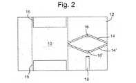
第2の実施形態の図2では、2つのVビームが、各々における増幅された動作が、他方におけるのものとは反対方向であるような方法で使用される。これは、2つのビームは反対かつ相等しい方向に偏るため、プルーフマス動作のさらに2倍の増幅を可能にする。この場合、ファブリペロー空洞は、2つのVビーム(14、14’)上に装着された鏡(16、16’)間に形成される。 In FIG. 2 of the second embodiment, two V beams are used in such a way that the amplified operation in each is in the opposite direction to that in the other. This allows for an additional amplification of twice the proof mass operation since the two beams are biased in opposite and equal directions. In this case, a Fabry-Perot cavity is formed between the mirrors (16, 16 ') mounted on the two V beams (14, 14').
単一Vビーム設計と比較して、2つのVビームを有する設計は、交差軸感度に関してより良好なパフォーマンスを与えるが、これは、鏡動作と同じ軸に沿ってかけられた加速は、両方のVビーム上に同じ影響を与えるはずであり、その結果空洞長さの変化を生じさせないためである。 Compared to the single V-beam design, the design with two V-beams gives better performance with respect to cross-axis sensitivity, which means that the acceleration applied along the same axis as the mirror motion is This is because it should have the same effect on the V-beam and as a result does not cause a change in cavity length.
図3では、第2のVビーム(24)が、第1のVビーム(14)の中央、および基板の壁に取り付けられる。これは、第1のVビームが偏ったときに第2がこの偏りを再増幅させる倍数的増幅を与える。第3のVビーム(34)は、第2のVビーム(24)の中央および基板の壁に取り付けられ、したがって、第1のVビーム(14)、第2のVビーム(24)および第3のVビーム(34)の偏りの累積効果によって引き起こされたさらなる倍数的増幅をもたらす。実際、基板の壁と前のVビームの頂点の間にすべて位置するVビーム(4)の「カスケード」を有することが可能である。これは、応答およびエッチングプロセスの両方において製造に複雑性を加え、極めて専門的な用途では頑強性を低減させることがあるが、必要とされる技術者の試みは、得られる利点によって正当化され得る。 In FIG. 3, a second V beam (24) is attached to the center of the first V beam (14) and to the wall of the substrate. This provides multiple amplification where the second re-amplifies this bias when the first V-beam is biased. The third V beam (34) is attached to the center of the second V beam (24) and to the wall of the substrate, and thus the first V beam (14), the second V beam (24) and the third V beam. Result in further multiple amplification caused by the cumulative effect of the V-beam (34) bias. In fact, it is possible to have a “cascade” of V-beams (4) located between the substrate wall and the vertices of the previous V-beam. While this adds complexity to manufacturing in both response and etch processes and may reduce robustness in highly specialized applications, the required technician attempt is justified by the benefits obtained. obtain.
この発明の別の実施形態では、Vビームまたはその複数のVビームの偏りの大きさは、プルーフマスの移動に対向する、アクチュエータによって発生させられた力の大きさを決定する。アクチュエータは、たとえば、静電アクチュエータまたは熱アクチュエータでよい。これは作動の閉ループモード内で起こり、それにより、Vビームまたはその複数のVビームの偏りが、加速度計が非線形モードで作動することを防止するために必要とされる力の大きさを連続的に決定する。加速度は、したがって、アクチュエータによってかけられた力の大きさを測定することによってさらに確実にされ得る。 In another embodiment of the invention, the magnitude of the bias of the V-beam or the plurality of V-beams determines the magnitude of the force generated by the actuator that opposes the movement of the proof mass. The actuator may be, for example, an electrostatic actuator or a thermal actuator. This occurs within a closed-loop mode of operation, whereby the bias of the V-beam or its multiple V-beams continuously increases the amount of force required to prevent the accelerometer from operating in a non-linear mode. To decide. The acceleration can therefore be further ensured by measuring the magnitude of the force exerted by the actuator.
Claims (11)
Translated fromJapaneseApplications Claiming Priority (3)
| Application Number | Priority Date | Filing Date | Title |
|---|---|---|---|
| GB1200521.1 | 2012-01-13 | ||
| GB1200521.1AGB2498520A (en) | 2012-01-13 | 2012-01-13 | Accelerometer |
| PCT/GB2013/000012WO2013104890A1 (en) | 2012-01-13 | 2013-01-11 | Improvements in accelerometers |
Publications (2)
| Publication Number | Publication Date |
|---|---|
| JP2015503759A JP2015503759A (en) | 2015-02-02 |
| JP6082028B2true JP6082028B2 (en) | 2017-02-15 |
Family
ID=45813948
Family Applications (1)
| Application Number | Title | Priority Date | Filing Date |
|---|---|---|---|
| JP2014551670AExpired - Fee RelatedJP6082028B2 (en) | 2012-01-13 | 2013-01-11 | Improvements in accelerometers |
Country Status (7)
| Country | Link |
|---|---|
| US (1) | US9470527B2 (en) |
| EP (1) | EP2802882A1 (en) |
| JP (1) | JP6082028B2 (en) |
| CN (1) | CN104169724B (en) |
| GB (2) | GB2498520A (en) |
| HK (1) | HK1203628A1 (en) |
| WO (1) | WO2013104890A1 (en) |
Families Citing this family (4)
| Publication number | Priority date | Publication date | Assignee | Title |
|---|---|---|---|---|
| GB2498520A (en)* | 2012-01-13 | 2013-07-24 | Secr Defence | Accelerometer |
| DE102015217430A1 (en)* | 2015-09-11 | 2017-03-16 | Siemens Aktiengesellschaft | Fiber optic acceleration sensor |
| CN111337701B (en)* | 2020-03-20 | 2023-08-04 | 南京智慧基础设施技术研究院有限公司 | Sensing device for acceleration detection |
| CN114034300A (en)* | 2021-11-09 | 2022-02-11 | 中国电子科技集团公司信息科学研究院 | Optical Accelerometers and Inertial Navigation Systems |
Family Cites Families (25)
| Publication number | Priority date | Publication date | Assignee | Title |
|---|---|---|---|---|
| EP0693690B1 (en)* | 1994-06-29 | 1999-04-28 | New Sd, Inc. | Accelerometer and method of manufacture |
| GB9416683D0 (en)* | 1994-08-18 | 1994-10-19 | British Tech Group | Accelerometer |
| US6046840A (en)* | 1995-06-19 | 2000-04-04 | Reflectivity, Inc. | Double substrate reflective spatial light modulator with self-limiting micro-mechanical elements |
| US6183097B1 (en)* | 1999-01-12 | 2001-02-06 | Cornell Research Foundation Inc. | Motion amplification based sensors |
| US6401536B1 (en)* | 2000-02-11 | 2002-06-11 | Motorola, Inc. | Acceleration sensor and method of manufacture |
| EP1311863A4 (en)* | 2000-06-21 | 2003-07-30 | Input Output Inc | Accelerometer with folded beams |
| WO2002057799A2 (en)* | 2001-01-17 | 2002-07-25 | Honeywell International Inc. | Accelerometer whose seismic mass is shaped as whiffletree |
| FR2821433B1 (en)* | 2001-02-26 | 2003-10-31 | Sagem | ACCELEROMETER FOR VIBRATING BLADES |
| US7428054B2 (en)* | 2002-10-15 | 2008-09-23 | University Of Maryland | Micro-optical sensor system for pressure, acceleration, and pressure gradient measurements |
| US6955085B2 (en)* | 2003-06-02 | 2005-10-18 | Weatherford/Lamb, Inc. | Optical accelerometer or displacement device using a flexure system |
| US7137299B2 (en)* | 2005-04-21 | 2006-11-21 | Northrop Grumman Corporation | Fiber optic accelerometer |
| US7583390B2 (en)* | 2006-03-02 | 2009-09-01 | Symphony Acoustics, Inc. | Accelerometer comprising an optically resonant cavity |
| US8261614B2 (en)* | 2006-03-10 | 2012-09-11 | Continental Teves Ag & Co. Ohg | Rotational speed sensor having a coupling bar |
| CN101131354A (en)* | 2006-08-23 | 2008-02-27 | 中国科学院微电子研究所 | A micro-cantilever beam sensor with a triangular structure and its manufacturing method |
| CA2569159C (en)* | 2006-11-28 | 2015-01-13 | Nanometrics Inc. | Inertial sensor |
| US20080289429A1 (en)* | 2007-05-22 | 2008-11-27 | Zhou Tiansheng | Fiber optic mems seismic sensor with mass supported by hinged beams |
| WO2008156018A1 (en)* | 2007-06-18 | 2008-12-24 | Alps Electric Co., Ltd. | Capacitance type acceleration sensor |
| US7661313B2 (en)* | 2007-11-05 | 2010-02-16 | The United States Of America As Represented By The Secretary Of The Navy | Acceleration strain transducer |
| CN101271124B (en)* | 2008-05-16 | 2010-09-29 | 中国科学院上海微系统与信息技术研究所 | L-shaped beam piezoresistive micro-accelerometer and manufacturing method thereof |
| JP5431076B2 (en)* | 2009-09-03 | 2014-03-05 | 日本発條株式会社 | Slide structure for vehicle seat |
| JP2011153836A (en)* | 2010-01-26 | 2011-08-11 | Seiko Epson Corp | Acceleration sensor, and accelerometer |
| CN101858929B (en)* | 2010-05-21 | 2012-09-05 | 中国科学院上海微系统与信息技术研究所 | Capacitive micro-acceleration sensor with symmetrically combined elastic beam structure and production method thereof |
| US8904867B2 (en)* | 2010-11-04 | 2014-12-09 | Qualcomm Mems Technologies, Inc. | Display-integrated optical accelerometer |
| CN102128953B (en)* | 2010-12-10 | 2012-10-17 | 中国科学院上海微系统与信息技术研究所 | Capacitive micro-accelerometer with symmetrical tilted folded beam structure |
| GB2498520A (en)* | 2012-01-13 | 2013-07-24 | Secr Defence | Accelerometer |
- 2012
- 2012-01-13GBGB1200521.1Apatent/GB2498520A/ennot_activeWithdrawn
- 2013
- 2013-01-11EPEP13703854.3Apatent/EP2802882A1/ennot_activeWithdrawn
- 2013-01-11CNCN201380013993.XApatent/CN104169724B/ennot_activeExpired - Fee Related
- 2013-01-11USUS14/371,225patent/US9470527B2/ennot_activeExpired - Fee Related
- 2013-01-11GBGB1300511.1Apatent/GB2498454B/enactiveActive
- 2013-01-11JPJP2014551670Apatent/JP6082028B2/ennot_activeExpired - Fee Related
- 2013-01-11HKHK15104167.2Apatent/HK1203628A1/enunknown
- 2013-01-11WOPCT/GB2013/000012patent/WO2013104890A1/enactiveApplication Filing
Also Published As
| Publication number | Publication date |
|---|---|
| EP2802882A1 (en) | 2014-11-19 |
| CN104169724A (en) | 2014-11-26 |
| GB2498454A (en) | 2013-07-17 |
| US9470527B2 (en) | 2016-10-18 |
| HK1203628A1 (en) | 2015-10-30 |
| WO2013104890A1 (en) | 2013-07-18 |
| GB2498520A (en) | 2013-07-24 |
| GB2498454B (en) | 2016-06-22 |
| US20140352432A1 (en) | 2014-12-04 |
| GB201300511D0 (en) | 2013-02-27 |
| CN104169724B (en) | 2016-12-07 |
| JP2015503759A (en) | 2015-02-02 |
| GB201200521D0 (en) | 2012-02-29 |
Similar Documents
| Publication | Publication Date | Title |
|---|---|---|
| US10126321B2 (en) | Micro-opto-electromechanical systems (MOEMS) device | |
| CA2921227C (en) | All-optical system responsive to motion and optical module for use in the same | |
| US7518731B2 (en) | Interferometric MOEMS sensor | |
| Sabry et al. | Monolithic silicon‐micromachined free‐space optical interferometers onchip | |
| EP2859302B1 (en) | Optical accelerometer system | |
| US10401377B2 (en) | Optical sensor system and methods of use thereof | |
| EP1906159B1 (en) | System, method and apparatus for a micromachined interferometer using optical splitting | |
| EP3088905B1 (en) | System and methods for highly integrated optical readout mems sensors | |
| Davies et al. | MEMS Fabry–Pérot optical accelerometer employing mechanical amplification via a V-beam structure | |
| US5689107A (en) | Displacement-based opto-electronic accelerometer and pressure sensor | |
| JP6082028B2 (en) | Improvements in accelerometers | |
| Taghavi et al. | Simulation, fabrication, and characterization of a sensitive SU-8-based Fabry-Pérot MOEMS accelerometer | |
| CN112313488A (en) | Interferometer and method for producing an interferometer | |
| CN112816737A (en) | Accelerometer based on hemispherical FP (Fabry-Perot) cavity on-chip integrated optical machine and manufacturing method | |
| KR102694949B1 (en) | Optical fiber sensor-based inertial measurement system | |
| Zhang et al. | Integrated Micro Sensor Based on Grating Interferometer: A Review | |
| CN118518902A (en) | Semiconductor structure, acceleration detection method thereof and optical coupling packaging combination | |
| Zandi et al. | VOA-based optical MEMS accelerometer | |
| CN117092369A (en) | Optical resonance accelerometer based on wide-spectrum light source | |
| AboZyd et al. | Tri-axial optical MEMS accelerometer enables monolithic fabrication | |
| Rahimi et al. | The design and simulation of a coarse-to-fine optical MEMS accelerometer | |
| CN120468458B (en) | Acceleration sensor and preparation method thereof, and acceleration sensing system | |
| KR101283924B1 (en) | A micro accelerometer using a liquid metal droplet and Fabry-Perot interferometry | |
| Nayak et al. | Design and analysis of micro-opto-electro-mechanical accelerometer | |
| CN113884703A (en) | Triaxial fiber accelerometer |
Legal Events
| Date | Code | Title | Description |
|---|---|---|---|
| A621 | Written request for application examination | Free format text:JAPANESE INTERMEDIATE CODE: A621 Effective date:20150903 | |
| A977 | Report on retrieval | Free format text:JAPANESE INTERMEDIATE CODE: A971007 Effective date:20160615 | |
| A131 | Notification of reasons for refusal | Free format text:JAPANESE INTERMEDIATE CODE: A131 Effective date:20160705 | |
| A521 | Request for written amendment filed | Free format text:JAPANESE INTERMEDIATE CODE: A523 Effective date:20160928 | |
| TRDD | Decision of grant or rejection written | ||
| A01 | Written decision to grant a patent or to grant a registration (utility model) | Free format text:JAPANESE INTERMEDIATE CODE: A01 Effective date:20170110 | |
| A61 | First payment of annual fees (during grant procedure) | Free format text:JAPANESE INTERMEDIATE CODE: A61 Effective date:20170119 | |
| R150 | Certificate of patent or registration of utility model | Ref document number:6082028 Country of ref document:JP Free format text:JAPANESE INTERMEDIATE CODE: R150 | |
| R250 | Receipt of annual fees | Free format text:JAPANESE INTERMEDIATE CODE: R250 | |
| LAPS | Cancellation because of no payment of annual fees |